US6646289B1 - Integrated circuit device - Google Patents
Integrated circuit deviceDownload PDFInfo
- Publication number
- US6646289B1 US6646289B1US09/601,895US60189500AUS6646289B1US 6646289 B1US6646289 B1US 6646289B1US 60189500 AUS60189500 AUS 60189500AUS 6646289 B1US6646289 B1US 6646289B1
- Authority
- US
- United States
- Prior art keywords
- integrated circuit
- circuit device
- integrally packaged
- packaged optronic
- transparent protective
- Prior art date
- Legal status (The legal status is an assumption and is not a legal conclusion. Google has not performed a legal analysis and makes no representation as to the accuracy of the status listed.)
- Expired - Lifetime
Links
Images


Classifications
- H—ELECTRICITY
- H10—SEMICONDUCTOR DEVICES; ELECTRIC SOLID-STATE DEVICES NOT OTHERWISE PROVIDED FOR
- H10F—INORGANIC SEMICONDUCTOR DEVICES SENSITIVE TO INFRARED RADIATION, LIGHT, ELECTROMAGNETIC RADIATION OF SHORTER WAVELENGTH OR CORPUSCULAR RADIATION
- H10F77/00—Constructional details of devices covered by this subclass
- H10F77/93—Interconnections
- H—ELECTRICITY
- H01—ELECTRIC ELEMENTS
- H01L—SEMICONDUCTOR DEVICES NOT COVERED BY CLASS H10
- H01L21/00—Processes or apparatus adapted for the manufacture or treatment of semiconductor or solid state devices or of parts thereof
- H01L21/02—Manufacture or treatment of semiconductor devices or of parts thereof
- H01L21/04—Manufacture or treatment of semiconductor devices or of parts thereof the devices having potential barriers, e.g. a PN junction, depletion layer or carrier concentration layer
- H01L21/50—Assembly of semiconductor devices using processes or apparatus not provided for in a single one of the groups H01L21/18 - H01L21/326 or H10D48/04 - H10D48/07 e.g. sealing of a cap to a base of a container
- H01L21/56—Encapsulations, e.g. encapsulation layers, coatings
- H—ELECTRICITY
- H01—ELECTRIC ELEMENTS
- H01L—SEMICONDUCTOR DEVICES NOT COVERED BY CLASS H10
- H01L23/00—Details of semiconductor or other solid state devices
- H01L23/28—Encapsulations, e.g. encapsulating layers, coatings, e.g. for protection
- H01L23/31—Encapsulations, e.g. encapsulating layers, coatings, e.g. for protection characterised by the arrangement or shape
- H01L23/3107—Encapsulations, e.g. encapsulating layers, coatings, e.g. for protection characterised by the arrangement or shape the device being completely enclosed
- H01L23/3114—Encapsulations, e.g. encapsulating layers, coatings, e.g. for protection characterised by the arrangement or shape the device being completely enclosed the device being a chip scale package, e.g. CSP
- H—ELECTRICITY
- H01—ELECTRIC ELEMENTS
- H01L—SEMICONDUCTOR DEVICES NOT COVERED BY CLASS H10
- H01L24/00—Arrangements for connecting or disconnecting semiconductor or solid-state bodies; Methods or apparatus related thereto
- H01L24/01—Means for bonding being attached to, or being formed on, the surface to be connected, e.g. chip-to-package, die-attach, "first-level" interconnects; Manufacturing methods related thereto
- H01L24/02—Bonding areas ; Manufacturing methods related thereto
- H—ELECTRICITY
- H01—ELECTRIC ELEMENTS
- H01L—SEMICONDUCTOR DEVICES NOT COVERED BY CLASS H10
- H01L24/00—Arrangements for connecting or disconnecting semiconductor or solid-state bodies; Methods or apparatus related thereto
- H01L24/93—Batch processes
- H01L24/95—Batch processes at chip-level, i.e. with connecting carried out on a plurality of singulated devices, i.e. on diced chips
- H01L24/97—Batch processes at chip-level, i.e. with connecting carried out on a plurality of singulated devices, i.e. on diced chips the devices being connected to a common substrate, e.g. interposer, said common substrate being separable into individual assemblies after connecting
- H—ELECTRICITY
- H10—SEMICONDUCTOR DEVICES; ELECTRIC SOLID-STATE DEVICES NOT OTHERWISE PROVIDED FOR
- H10D—INORGANIC ELECTRIC SEMICONDUCTOR DEVICES
- H10D84/00—Integrated devices formed in or on semiconductor substrates that comprise only semiconducting layers, e.g. on Si wafers or on GaAs-on-Si wafers
- H10D84/01—Manufacture or treatment
- H—ELECTRICITY
- H10—SEMICONDUCTOR DEVICES; ELECTRIC SOLID-STATE DEVICES NOT OTHERWISE PROVIDED FOR
- H10F—INORGANIC SEMICONDUCTOR DEVICES SENSITIVE TO INFRARED RADIATION, LIGHT, ELECTROMAGNETIC RADIATION OF SHORTER WAVELENGTH OR CORPUSCULAR RADIATION
- H10F39/00—Integrated devices, or assemblies of multiple devices, comprising at least one element covered by group H10F30/00, e.g. radiation detectors comprising photodiode arrays
- H10F39/011—Manufacture or treatment of image sensors covered by group H10F39/12
- H10F39/026—Wafer-level processing
- H—ELECTRICITY
- H10—SEMICONDUCTOR DEVICES; ELECTRIC SOLID-STATE DEVICES NOT OTHERWISE PROVIDED FOR
- H10F—INORGANIC SEMICONDUCTOR DEVICES SENSITIVE TO INFRARED RADIATION, LIGHT, ELECTROMAGNETIC RADIATION OF SHORTER WAVELENGTH OR CORPUSCULAR RADIATION
- H10F39/00—Integrated devices, or assemblies of multiple devices, comprising at least one element covered by group H10F30/00, e.g. radiation detectors comprising photodiode arrays
- H10F39/80—Constructional details of image sensors
- H10F39/804—Containers or encapsulations
- H—ELECTRICITY
- H10—SEMICONDUCTOR DEVICES; ELECTRIC SOLID-STATE DEVICES NOT OTHERWISE PROVIDED FOR
- H10F—INORGANIC SEMICONDUCTOR DEVICES SENSITIVE TO INFRARED RADIATION, LIGHT, ELECTROMAGNETIC RADIATION OF SHORTER WAVELENGTH OR CORPUSCULAR RADIATION
- H10F55/00—Radiation-sensitive semiconductor devices covered by groups H10F10/00, H10F19/00 or H10F30/00 being structurally associated with electric light sources and electrically or optically coupled thereto
- H10F55/18—Radiation-sensitive semiconductor devices covered by groups H10F10/00, H10F19/00 or H10F30/00 being structurally associated with electric light sources and electrically or optically coupled thereto wherein the radiation-sensitive semiconductor devices and the electric light source share a common body having dual-functionality of light emission and light detection
- H—ELECTRICITY
- H10—SEMICONDUCTOR DEVICES; ELECTRIC SOLID-STATE DEVICES NOT OTHERWISE PROVIDED FOR
- H10F—INORGANIC SEMICONDUCTOR DEVICES SENSITIVE TO INFRARED RADIATION, LIGHT, ELECTROMAGNETIC RADIATION OF SHORTER WAVELENGTH OR CORPUSCULAR RADIATION
- H10F71/00—Manufacture or treatment of devices covered by this subclass
- H—ELECTRICITY
- H10—SEMICONDUCTOR DEVICES; ELECTRIC SOLID-STATE DEVICES NOT OTHERWISE PROVIDED FOR
- H10F—INORGANIC SEMICONDUCTOR DEVICES SENSITIVE TO INFRARED RADIATION, LIGHT, ELECTROMAGNETIC RADIATION OF SHORTER WAVELENGTH OR CORPUSCULAR RADIATION
- H10F77/00—Constructional details of devices covered by this subclass
- H10F77/30—Coatings
- H10F77/306—Coatings for devices having potential barriers
- H10F77/331—Coatings for devices having potential barriers for filtering or shielding light, e.g. multicolour filters for photodetectors
- H10F77/334—Coatings for devices having potential barriers for filtering or shielding light, e.g. multicolour filters for photodetectors for shielding light, e.g. light blocking layers or cold shields for infrared detectors
- H—ELECTRICITY
- H10—SEMICONDUCTOR DEVICES; ELECTRIC SOLID-STATE DEVICES NOT OTHERWISE PROVIDED FOR
- H10F—INORGANIC SEMICONDUCTOR DEVICES SENSITIVE TO INFRARED RADIATION, LIGHT, ELECTROMAGNETIC RADIATION OF SHORTER WAVELENGTH OR CORPUSCULAR RADIATION
- H10F77/00—Constructional details of devices covered by this subclass
- H10F77/40—Optical elements or arrangements
- H10F77/413—Optical elements or arrangements directly associated or integrated with the devices, e.g. back reflectors
- H—ELECTRICITY
- H10—SEMICONDUCTOR DEVICES; ELECTRIC SOLID-STATE DEVICES NOT OTHERWISE PROVIDED FOR
- H10F—INORGANIC SEMICONDUCTOR DEVICES SENSITIVE TO INFRARED RADIATION, LIGHT, ELECTROMAGNETIC RADIATION OF SHORTER WAVELENGTH OR CORPUSCULAR RADIATION
- H10F77/00—Constructional details of devices covered by this subclass
- H10F77/50—Encapsulations or containers
- H—ELECTRICITY
- H10—SEMICONDUCTOR DEVICES; ELECTRIC SOLID-STATE DEVICES NOT OTHERWISE PROVIDED FOR
- H10H—INORGANIC LIGHT-EMITTING SEMICONDUCTOR DEVICES HAVING POTENTIAL BARRIERS
- H10H20/00—Individual inorganic light-emitting semiconductor devices having potential barriers, e.g. light-emitting diodes [LED]
- H10H20/01—Manufacture or treatment
- H—ELECTRICITY
- H10—SEMICONDUCTOR DEVICES; ELECTRIC SOLID-STATE DEVICES NOT OTHERWISE PROVIDED FOR
- H10H—INORGANIC LIGHT-EMITTING SEMICONDUCTOR DEVICES HAVING POTENTIAL BARRIERS
- H10H20/00—Individual inorganic light-emitting semiconductor devices having potential barriers, e.g. light-emitting diodes [LED]
- H10H20/80—Constructional details
- H10H20/84—Coatings, e.g. passivation layers or antireflective coatings
- H—ELECTRICITY
- H10—SEMICONDUCTOR DEVICES; ELECTRIC SOLID-STATE DEVICES NOT OTHERWISE PROVIDED FOR
- H10H—INORGANIC LIGHT-EMITTING SEMICONDUCTOR DEVICES HAVING POTENTIAL BARRIERS
- H10H20/00—Individual inorganic light-emitting semiconductor devices having potential barriers, e.g. light-emitting diodes [LED]
- H10H20/80—Constructional details
- H10H20/85—Packages
- H10H20/8506—Containers
- H—ELECTRICITY
- H10—SEMICONDUCTOR DEVICES; ELECTRIC SOLID-STATE DEVICES NOT OTHERWISE PROVIDED FOR
- H10H—INORGANIC LIGHT-EMITTING SEMICONDUCTOR DEVICES HAVING POTENTIAL BARRIERS
- H10H20/00—Individual inorganic light-emitting semiconductor devices having potential barriers, e.g. light-emitting diodes [LED]
- H10H20/80—Constructional details
- H10H20/85—Packages
- H10H20/852—Encapsulations
- H10H20/854—Encapsulations characterised by their material, e.g. epoxy or silicone resins
- H—ELECTRICITY
- H10—SEMICONDUCTOR DEVICES; ELECTRIC SOLID-STATE DEVICES NOT OTHERWISE PROVIDED FOR
- H10H—INORGANIC LIGHT-EMITTING SEMICONDUCTOR DEVICES HAVING POTENTIAL BARRIERS
- H10H29/00—Integrated devices, or assemblies of multiple devices, comprising at least one light-emitting semiconductor element covered by group H10H20/00
- H10H29/10—Integrated devices comprising at least one light-emitting semiconductor component covered by group H10H20/00
- H—ELECTRICITY
- H01—ELECTRIC ELEMENTS
- H01L—SEMICONDUCTOR DEVICES NOT COVERED BY CLASS H10
- H01L2221/00—Processes or apparatus adapted for the manufacture or treatment of semiconductor or solid state devices or of parts thereof covered by H01L21/00
- H01L2221/67—Apparatus for handling semiconductor or electric solid state devices during manufacture or treatment thereof; Apparatus for handling wafers during manufacture or treatment of semiconductor or electric solid state devices or components; Apparatus not specifically provided for elsewhere
- H01L2221/683—Apparatus for handling semiconductor or electric solid state devices during manufacture or treatment thereof; Apparatus for handling wafers during manufacture or treatment of semiconductor or electric solid state devices or components; Apparatus not specifically provided for elsewhere for supporting or gripping
- H01L2221/68304—Apparatus for handling semiconductor or electric solid state devices during manufacture or treatment thereof; Apparatus for handling wafers during manufacture or treatment of semiconductor or electric solid state devices or components; Apparatus not specifically provided for elsewhere for supporting or gripping using temporarily an auxiliary support
- H01L2221/68327—Apparatus for handling semiconductor or electric solid state devices during manufacture or treatment thereof; Apparatus for handling wafers during manufacture or treatment of semiconductor or electric solid state devices or components; Apparatus not specifically provided for elsewhere for supporting or gripping using temporarily an auxiliary support used during dicing or grinding
- H—ELECTRICITY
- H01—ELECTRIC ELEMENTS
- H01L—SEMICONDUCTOR DEVICES NOT COVERED BY CLASS H10
- H01L2224/00—Indexing scheme for arrangements for connecting or disconnecting semiconductor or solid-state bodies and methods related thereto as covered by H01L24/00
- H01L2224/01—Means for bonding being attached to, or being formed on, the surface to be connected, e.g. chip-to-package, die-attach, "first-level" interconnects; Manufacturing methods related thereto
- H01L2224/02—Bonding areas; Manufacturing methods related thereto
- H01L2224/04—Structure, shape, material or disposition of the bonding areas prior to the connecting process
- H01L2224/0401—Bonding areas specifically adapted for bump connectors, e.g. under bump metallisation [UBM]
- H—ELECTRICITY
- H01—ELECTRIC ELEMENTS
- H01L—SEMICONDUCTOR DEVICES NOT COVERED BY CLASS H10
- H01L2224/00—Indexing scheme for arrangements for connecting or disconnecting semiconductor or solid-state bodies and methods related thereto as covered by H01L24/00
- H01L2224/01—Means for bonding being attached to, or being formed on, the surface to be connected, e.g. chip-to-package, die-attach, "first-level" interconnects; Manufacturing methods related thereto
- H01L2224/18—High density interconnect [HDI] connectors; Manufacturing methods related thereto
- H01L2224/23—Structure, shape, material or disposition of the high density interconnect connectors after the connecting process
- H01L2224/24—Structure, shape, material or disposition of the high density interconnect connectors after the connecting process of an individual high density interconnect connector
- H01L2224/2405—Shape
- H01L2224/24051—Conformal with the semiconductor or solid-state device
- H—ELECTRICITY
- H01—ELECTRIC ELEMENTS
- H01L—SEMICONDUCTOR DEVICES NOT COVERED BY CLASS H10
- H01L2224/00—Indexing scheme for arrangements for connecting or disconnecting semiconductor or solid-state bodies and methods related thereto as covered by H01L24/00
- H01L2224/01—Means for bonding being attached to, or being formed on, the surface to be connected, e.g. chip-to-package, die-attach, "first-level" interconnects; Manufacturing methods related thereto
- H01L2224/18—High density interconnect [HDI] connectors; Manufacturing methods related thereto
- H01L2224/23—Structure, shape, material or disposition of the high density interconnect connectors after the connecting process
- H01L2224/24—Structure, shape, material or disposition of the high density interconnect connectors after the connecting process of an individual high density interconnect connector
- H01L2224/241—Disposition
- H01L2224/24151—Connecting between a semiconductor or solid-state body and an item not being a semiconductor or solid-state body, e.g. chip-to-substrate, chip-to-passive
- H01L2224/24221—Connecting between a semiconductor or solid-state body and an item not being a semiconductor or solid-state body, e.g. chip-to-substrate, chip-to-passive the body and the item being stacked
- H01L2224/24225—Connecting between a semiconductor or solid-state body and an item not being a semiconductor or solid-state body, e.g. chip-to-substrate, chip-to-passive the body and the item being stacked the item being non-metallic, e.g. insulating substrate with or without metallisation
- H—ELECTRICITY
- H01—ELECTRIC ELEMENTS
- H01L—SEMICONDUCTOR DEVICES NOT COVERED BY CLASS H10
- H01L2224/00—Indexing scheme for arrangements for connecting or disconnecting semiconductor or solid-state bodies and methods related thereto as covered by H01L24/00
- H01L2224/93—Batch processes
- H01L2224/94—Batch processes at wafer-level, i.e. with connecting carried out on a wafer comprising a plurality of undiced individual devices
- H—ELECTRICITY
- H01—ELECTRIC ELEMENTS
- H01L—SEMICONDUCTOR DEVICES NOT COVERED BY CLASS H10
- H01L2224/00—Indexing scheme for arrangements for connecting or disconnecting semiconductor or solid-state bodies and methods related thereto as covered by H01L24/00
- H01L2224/93—Batch processes
- H01L2224/95—Batch processes at chip-level, i.e. with connecting carried out on a plurality of singulated devices, i.e. on diced chips
- H01L2224/97—Batch processes at chip-level, i.e. with connecting carried out on a plurality of singulated devices, i.e. on diced chips the devices being connected to a common substrate, e.g. interposer, said common substrate being separable into individual assemblies after connecting
- H—ELECTRICITY
- H01—ELECTRIC ELEMENTS
- H01L—SEMICONDUCTOR DEVICES NOT COVERED BY CLASS H10
- H01L24/00—Arrangements for connecting or disconnecting semiconductor or solid-state bodies; Methods or apparatus related thereto
- H01L24/01—Means for bonding being attached to, or being formed on, the surface to be connected, e.g. chip-to-package, die-attach, "first-level" interconnects; Manufacturing methods related thereto
- H01L24/18—High density interconnect [HDI] connectors; Manufacturing methods related thereto
- H01L24/23—Structure, shape, material or disposition of the high density interconnect connectors after the connecting process
- H01L24/24—Structure, shape, material or disposition of the high density interconnect connectors after the connecting process of an individual high density interconnect connector
- H—ELECTRICITY
- H01—ELECTRIC ELEMENTS
- H01L—SEMICONDUCTOR DEVICES NOT COVERED BY CLASS H10
- H01L24/00—Arrangements for connecting or disconnecting semiconductor or solid-state bodies; Methods or apparatus related thereto
- H01L24/80—Methods for connecting semiconductor or other solid state bodies using means for bonding being attached to, or being formed on, the surface to be connected
- H01L24/82—Methods for connecting semiconductor or other solid state bodies using means for bonding being attached to, or being formed on, the surface to be connected by forming build-up interconnects at chip-level, e.g. for high density interconnects [HDI]
- H—ELECTRICITY
- H01—ELECTRIC ELEMENTS
- H01L—SEMICONDUCTOR DEVICES NOT COVERED BY CLASS H10
- H01L25/00—Assemblies consisting of a plurality of semiconductor or other solid state devices
- H01L25/03—Assemblies consisting of a plurality of semiconductor or other solid state devices all the devices being of a type provided for in a single subclass of subclasses H10B, H10D, H10F, H10H, H10K or H10N, e.g. assemblies of rectifier diodes
- H01L25/10—Assemblies consisting of a plurality of semiconductor or other solid state devices all the devices being of a type provided for in a single subclass of subclasses H10B, H10D, H10F, H10H, H10K or H10N, e.g. assemblies of rectifier diodes the devices having separate containers
- H01L25/105—Assemblies consisting of a plurality of semiconductor or other solid state devices all the devices being of a type provided for in a single subclass of subclasses H10B, H10D, H10F, H10H, H10K or H10N, e.g. assemblies of rectifier diodes the devices having separate containers the devices being integrated devices of class H10
- H—ELECTRICITY
- H01—ELECTRIC ELEMENTS
- H01L—SEMICONDUCTOR DEVICES NOT COVERED BY CLASS H10
- H01L2924/00—Indexing scheme for arrangements or methods for connecting or disconnecting semiconductor or solid-state bodies as covered by H01L24/00
- H01L2924/01—Chemical elements
- H01L2924/01005—Boron [B]
- H—ELECTRICITY
- H01—ELECTRIC ELEMENTS
- H01L—SEMICONDUCTOR DEVICES NOT COVERED BY CLASS H10
- H01L2924/00—Indexing scheme for arrangements or methods for connecting or disconnecting semiconductor or solid-state bodies as covered by H01L24/00
- H01L2924/01—Chemical elements
- H01L2924/01006—Carbon [C]
- H—ELECTRICITY
- H01—ELECTRIC ELEMENTS
- H01L—SEMICONDUCTOR DEVICES NOT COVERED BY CLASS H10
- H01L2924/00—Indexing scheme for arrangements or methods for connecting or disconnecting semiconductor or solid-state bodies as covered by H01L24/00
- H01L2924/01—Chemical elements
- H01L2924/01014—Silicon [Si]
- H—ELECTRICITY
- H01—ELECTRIC ELEMENTS
- H01L—SEMICONDUCTOR DEVICES NOT COVERED BY CLASS H10
- H01L2924/00—Indexing scheme for arrangements or methods for connecting or disconnecting semiconductor or solid-state bodies as covered by H01L24/00
- H01L2924/01—Chemical elements
- H01L2924/01027—Cobalt [Co]
- H—ELECTRICITY
- H01—ELECTRIC ELEMENTS
- H01L—SEMICONDUCTOR DEVICES NOT COVERED BY CLASS H10
- H01L2924/00—Indexing scheme for arrangements or methods for connecting or disconnecting semiconductor or solid-state bodies as covered by H01L24/00
- H01L2924/01—Chemical elements
- H01L2924/01029—Copper [Cu]
- H—ELECTRICITY
- H01—ELECTRIC ELEMENTS
- H01L—SEMICONDUCTOR DEVICES NOT COVERED BY CLASS H10
- H01L2924/00—Indexing scheme for arrangements or methods for connecting or disconnecting semiconductor or solid-state bodies as covered by H01L24/00
- H01L2924/01—Chemical elements
- H01L2924/01033—Arsenic [As]
- H—ELECTRICITY
- H01—ELECTRIC ELEMENTS
- H01L—SEMICONDUCTOR DEVICES NOT COVERED BY CLASS H10
- H01L2924/00—Indexing scheme for arrangements or methods for connecting or disconnecting semiconductor or solid-state bodies as covered by H01L24/00
- H01L2924/01—Chemical elements
- H01L2924/01051—Antimony [Sb]
- H—ELECTRICITY
- H01—ELECTRIC ELEMENTS
- H01L—SEMICONDUCTOR DEVICES NOT COVERED BY CLASS H10
- H01L2924/00—Indexing scheme for arrangements or methods for connecting or disconnecting semiconductor or solid-state bodies as covered by H01L24/00
- H01L2924/01—Chemical elements
- H01L2924/01057—Lanthanum [La]
- H—ELECTRICITY
- H01—ELECTRIC ELEMENTS
- H01L—SEMICONDUCTOR DEVICES NOT COVERED BY CLASS H10
- H01L2924/00—Indexing scheme for arrangements or methods for connecting or disconnecting semiconductor or solid-state bodies as covered by H01L24/00
- H01L2924/01—Chemical elements
- H01L2924/01068—Erbium [Er]
- H—ELECTRICITY
- H01—ELECTRIC ELEMENTS
- H01L—SEMICONDUCTOR DEVICES NOT COVERED BY CLASS H10
- H01L2924/00—Indexing scheme for arrangements or methods for connecting or disconnecting semiconductor or solid-state bodies as covered by H01L24/00
- H01L2924/01—Chemical elements
- H01L2924/01077—Iridium [Ir]
- H—ELECTRICITY
- H01—ELECTRIC ELEMENTS
- H01L—SEMICONDUCTOR DEVICES NOT COVERED BY CLASS H10
- H01L2924/00—Indexing scheme for arrangements or methods for connecting or disconnecting semiconductor or solid-state bodies as covered by H01L24/00
- H01L2924/01—Chemical elements
- H01L2924/01078—Platinum [Pt]
- H—ELECTRICITY
- H01—ELECTRIC ELEMENTS
- H01L—SEMICONDUCTOR DEVICES NOT COVERED BY CLASS H10
- H01L2924/00—Indexing scheme for arrangements or methods for connecting or disconnecting semiconductor or solid-state bodies as covered by H01L24/00
- H01L2924/01—Chemical elements
- H01L2924/01079—Gold [Au]
- H—ELECTRICITY
- H01—ELECTRIC ELEMENTS
- H01L—SEMICONDUCTOR DEVICES NOT COVERED BY CLASS H10
- H01L2924/00—Indexing scheme for arrangements or methods for connecting or disconnecting semiconductor or solid-state bodies as covered by H01L24/00
- H01L2924/013—Alloys
- H01L2924/014—Solder alloys
- H—ELECTRICITY
- H01—ELECTRIC ELEMENTS
- H01L—SEMICONDUCTOR DEVICES NOT COVERED BY CLASS H10
- H01L2924/00—Indexing scheme for arrangements or methods for connecting or disconnecting semiconductor or solid-state bodies as covered by H01L24/00
- H01L2924/10—Details of semiconductor or other solid state devices to be connected
- H01L2924/102—Material of the semiconductor or solid state bodies
- H01L2924/1025—Semiconducting materials
- H01L2924/10251—Elemental semiconductors, i.e. Group IV
- H01L2924/10253—Silicon [Si]
- H—ELECTRICITY
- H01—ELECTRIC ELEMENTS
- H01L—SEMICONDUCTOR DEVICES NOT COVERED BY CLASS H10
- H01L2924/00—Indexing scheme for arrangements or methods for connecting or disconnecting semiconductor or solid-state bodies as covered by H01L24/00
- H01L2924/10—Details of semiconductor or other solid state devices to be connected
- H01L2924/11—Device type
- H01L2924/14—Integrated circuits
- H—ELECTRICITY
- H10—SEMICONDUCTOR DEVICES; ELECTRIC SOLID-STATE DEVICES NOT OTHERWISE PROVIDED FOR
- H10H—INORGANIC LIGHT-EMITTING SEMICONDUCTOR DEVICES HAVING POTENTIAL BARRIERS
- H10H20/00—Individual inorganic light-emitting semiconductor devices having potential barriers, e.g. light-emitting diodes [LED]
- H10H20/80—Constructional details
- H10H20/85—Packages
- H10H20/857—Interconnections, e.g. lead-frames, bond wires or solder balls
Definitions
- the present inventionrelates to methods and apparatus for producing integrated circuit devices and to integrated circuit devices produced thereby and more particularly to an optronic integrally packaged die.
- PackagingAn essential step in the manufacture of all integrated circuit devices is known as “packaging” and involves mechanical and environmental protection of a silicon chip which is at the heart of the integrated circuit as well as electrical interconnection between predetermined locations on the silicon chip and external electrical terminals.
- Wire bondingemploys heat and ultrasonic energy to weld gold bonding wires between bond pads on the chip and contacts on the package.
- Tape automatic bondingemploys a copper foil tape instead of bonding wire.
- the copper foil tapeis configured for each specific die and package combination and includes a pattern of copper traces suited thereto.
- the individual leadsmay be connected individually or as a group to the various bond pads on the chip.
- Flip chipsare integrated circuit dies which have solder bumps formed on top of the bonding pads, thus allowing the die to be “flipped” circuit side down and directly soldered to a substrate. Wire bonds are not required and considerable savings in package spacing may be realized.
- Both wire bonding and TAB bondingare prone to bad bond formation and subject the die to relatively high temperatures and mechanical pressures.
- Both wire bond and TAB technologiesare problematic from a package size viewpoint, producing integrated circuit devices having a die-to-package area ratio ranging from about 10% to 60%.
- the flip-chipdoes not provide packaging but rather only interconnection.
- the interconnectionencounters problems of uniformity in the solder bumps as well as in thermal expansion mismatching, which limits the use of available substrates to silicon or materials which have thermal expansion characteristics similar to those of silicon.
- Optronic packages for semiconductorsare known.
- Conventional optronic packages used for imagingemploy a ceramic housing onto which is sealingly mounted a transparent window.
- Optronic packages used for low level imaging, light emission and radiation detection, including light detectionemploy a clear plastic enclosure.
- the present inventionseeks to provide optronic integrated circuit devices which are extremely compact as well as apparatus and techniques for the production thereof.
- an integrated circuit diecontaining at least one of a radiation emitter and radiation receiver and having top and bottom surfaces formed of electrically insulative and mechanically protective material, at least one of the surfaces being transparent to radiation, and electrically insulative edge surfaces having pads.
- the devicealso includes at least one spectral filter associated with a radiation transparent protective surface thereof.
- the deviceincludes a semiconductor substrate which is sufficiently thin as to enable to device to be responsive to back illumination.
- the devicealso includes at least one color filter associated with a radiation transparent protective surface thereof.
- lensesmay be integrally formed on a transparent protective surface of the device.
- light coupling bumpsmay be integrally formed on a transparent protective surface of the device.
- a waveguide and other optical componentsintegrally formed on a transparent protective surface of the device.
- an optical gratingmay be integrally formed on a transparent protective surface of the device.
- a polarizermay be formed on a transparent protective surface of the device.
- an integrated circuit diecontaining at least one of a radiation emitter and radiation receiver and having top and bottom surfaces formed of electrically insulative and mechanically protective material, at least one of the surfaces being transparent to radiation, the integrally packaged optronic integrated circuit device being characterized in that its longest dimension does not exceed the longest dimension of the die by more than 20%.
- the integrally packaged optronic integrated circuit deviceis characterized in that its longest dimension does not exceed the longest dimension of the die by more than 10%. More preferably the integrally packaged optronic integrated circuit device is characterized in that its longest dimension does not exceed the longest dimension of the die by more than 5%.
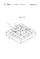
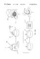
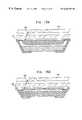
- FIGS. 1A and 1Bare respective top view and bottom view simplified pictorial illustrations of an integrally packaged optronic integrated circuit device constructed and operative in accordance with a preferred embodiment of the present invention
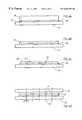
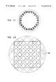
- FIG. 1Cis a bottom view simplified pictorial illustration of an integrally packaged optronic integrated circuit device of the type shown in FIGS. 1A and 1B, constructed and operative in accordance with another preferred embodiment of the present invention
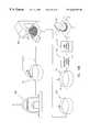
- FIG. 2is a simplified pictorial illustration of the attachment of a transparent protective packaging layer to a wafer containing a plurality of integrated circuit dies;
- FIG. 3is a simplified pictorial illustration of showing the individual dies on the wafer as seen through the transparent protective packaging layer attached thereto;
- FIGS. 4A, 4 B, 4 C and 4 Dare sectional illustrations of various stages in the manufacture of integrally packaged optronic integrated circuit devices in accordance with a preferred embodiment of the present invention
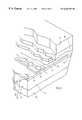
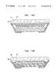
- FIG. 5is a partially cut away detailed pictorial illustration of n integrally packaged optronic integrated circuit vice produced from the wafer of FIG. 4D;
- FIGS. 6 7 A, 7 B 8 A and 8 Bare sectional illustrations of various stages in the manufacture of the integrally packaged optronic integrated circuit device shown in FIGS. 1A, 1 B, 1 C & 5 ;
- FIGS. 9, 10 A and 10 Btogether provide a simplified block diagram illustration of apparatus for carrying out the method of the present invention
- FIGS. 11A, 11 B, 11 C, 11 D an 11 Ea simplified pictorial illustrations of five alternative embodiments of an integrated circuit device constructed and operative in accordance with yet another preferred embodiment of the present invention and including spectral filters and/or anti-reflective coatings;
- FIGS. 12A, 12 B and 12 Care simplified pictorial illustrations of three alternative embodiments of an integrally packaged optronic integrated circuit device which is designed for back illumination;
- FIGS. 13A 13 B and 13 Care simplified pictorial illustrations of three alternative embodiments of an integrally packaged optronic integrated circuit device constructed and operative in accordance with still another preferred embodiment of the present invention wherein color array filters are integrated with the integrally packaged optronic integrated circuit device;
- FIGS. 14A, 14 B, 14 C and 14 Dare simplified pictorial illustrations of four alternative embodiments of an integrally packaged optronic integrated circuit device constructed and operative in accordance with another preferred embodiment of the present invention having lenses integrally formed on a transparent protective surface thereof;
- FIGS. 15A and 5Bare simplified pictorial illustration of two alternative embodiments of an integrally packaged optronic integrated circuit device constructed and operative in accordance with another preferred embodiment of the present invention having light coupling bumps integrally formed on a transparent protective surface thereof;
- FIGS. 16A and 16Bare simplified pictorial illustrations of two alternative embodiments of an integrally packaged optronic integrated circuit device constructed and operative in accordance with yet another preferred embodiment of the present invention having a waveguide and other optical components integrally formed on a transparent protective surface thereof;
- FIGS. 17A and 17Bare simplified pictorial illustrations of two alternative embodiments of an integrally packaged optronic integrated circuit device constructed and operative in accordance with still another preferred embodiment of the present invention wherein a polarizer is integrated with the integrally packaged optronic integrated circuit device;
- FIGS. 18A and 18Bare simplified pictorial illustrations of two alternative embodiments of an integrally packaged optronic integrated circuit device constructed and operative in accordance with still another preferred embodiment of the present invention wherein an optical grating is integrated with the integrally packaged optronic integrated circuit device.
- FIGS. 19A and 19Bare simplified pictorial illustrations of two alternative embodiments of an integrally packaged optronic integrated circuit device constructed and operative in accordance with yet another preferred embodiment of the present invention wherein the package is formed with a desired geometrical configuration;
- FIGS. 20A and 20Bare simplified pictorial illustrations of two alternative embodiments of an integrally packaged optronic integrated circuit device constructed and operative in accordance with yet another preferred embodiment of the present invention wherein edges of the package are coated with an opaque coating;
- FIG. 21is a simplified pictorial illustration of an integrally packaged optronic integrated circuit device constructed and operative in accordance with still another preferred embodiment of the present invention and having an octagonal configuration
- FIG. 22is a simplified pictorial illustration of a cutting pattern employed to produce integrated circuits of the type shown in FIG. 21 .
- FIGS. 1A-22illustrate the production of integrated circuit devices in accordance with a preferred embodiment of the present invention.
- the integrated circuit deviceincludes a relatively thin and compact, environmentally protected and mechanically strengthened integrated circuit package 10 having a multiplicity of electrical contacts 12 plated along the edge surfaces 14 thereof.
- contacts 12extend over edge surfaces onto the planar surfaces 16 of the package.
- This contact arrangementpermits both flat surface mounting and edge mounting of package 10 onto a circuit board.
- the integrated circuit package 10may include one or more of the following elements (not shown): an integrally formed dichroic filter, color filter, antireflective coating, polarizer, optical grating, integrated wave guide and optical coupling bumps.
- FIG. 1Cillustrates an alternative embodiment of the present invention wherein solderable bumps 17 are provided at the ends of each contact 12 .
- the solderable bumps 17are arranged in a predetermined array.
- a complete silicon wafer 20 having a plurality of finished dies 22 formed thereon by conventional techniquesis bonded at its active surface 24 to a radiation transparent protective insulating cover plate 26 via a layer 28 of epoxy.
- the insulating cover plate 26typically comprises glass, quartz, sapphire or any other suitable radiation transparent insulative substrate.
- the cover plate 26may be colored or tinted in order to operate as a spectral filter.
- a dichroic or colored spectral filtermay be formed on at least one surface of the cover plate 26 .
- cover plate 26 and epoxy layer 28are preferably transparent to radiation in a spectral region useful for optronic applications.
- the complete silicon wafer 20may be formed with an integral color filter array by conventional lithography techniques at any suitable location therein.
- a filtermay be formed and configured by conventional techniques over the cover plate 26 , such that the filter plane lies between cover plate 26 and the epoxy layer 28 .
- the silicon waferis preferably ground down to a decreased thickness, typically 100 microns, as shown in FIG. 4 B. This reduction in wafer thickness is enabled by the additional mechanical strength provided by the bonding thereof of the insulating cover plate 26 .
- the waferis etched, using a photolithography process, along its back surface along predetermined dice lines which separate the individual dies. Etched channels 30 are thus produced, which extend entirely through the thickness of the silicon substrate, typically 100 microns.
- the etched waferis shown in FIG. 4 C.
- the aforementioned etchingtypically takes place in conventional silicon etching solution, such as a combination of 2.5% hydrofluoric acid, 50% nitric acid, 10% acetic acid and 37.5% water, so as to etch the silicon down to the field oxide layer, as shown in FIG. 4 C.
- conventional silicon etching solutionsuch as a combination of 2.5% hydrofluoric acid, 50% nitric acid, 10% acetic acid and 37.5% water, so as to etch the silicon down to the field oxide layer, as shown in FIG. 4 C.
- the result of the silicon etchingis a plurality of separated dies 40 , each of which includes silicon of thickness about 100 microns.
- a second insulating packaging layer 42is bonded over the dies 40 on the side thereof opposite to insulating packaging layer 26 .
- a layer 44 of epoxylies between the dies 40 and the layer 42 and epoxy also fills the interstices between dies 40 .
- the packaging layer 42 and the epoxy layer 44are both transparent.
- lines 50lie along the interstices between adjacent dies 40 to define notches along the outlines of a plurality of pre-packaged integrated circuits. It is a particular feature of the invention that lines 50 are selected such that the edges of the dies along the notches are distanced from the outer extent of the silicon 40 by at least a distance d, as shown in FIGS. 4D and 5, to which reference is now additionally made.
- At least one insulating layer, including the field oxide layer,is shown at reference numeral 32 and metal pads are shown at reference numeral 34 .
- An over-metal insulating layeris shown at reference numeral 36 .
- the color filter planeis shown at reference numeral 38 .
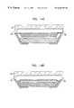
- FIGS. 6, 7 A, 7 B, 8 A and 8 Billustrate further steps in the manufacture of integrated circuit devices in accordance with a preferred embodiment of the present invention.
- FIG. 6illustrates at reference numeral 54 , a preferred cross sectional configuration of a notch produced by partially cutting as described hereinabove in connection with FIG. 5 .
- Vertical lines 56indicate the intersection of the notch 54 with the pads 34 , defining exposed sectional pad surfaces 51 .
- Vertical lines 58indicate the location of a subsequent final cut which separates the dies into individual integrated circuits at a later stage.
- FIGS. 7A and 7Billustrate the formation of metal contacts 12 along the inclined edges 14 and part of the top surface 16 . These contacts, which may be formed by any suitable metal deposition technique, are seen to extend inside notch 54 , thus establishing electrical contact with surfaces 51 of pads 34 .
- FIG. 7Ashows a configuration corresponding to that of FIGS. 1A and 1B without solderable bumps, while FIG. 7B shows the provision of solderable bumps 17 on contacts 12 , as illustrated in FIG. 1 C.
- metal contactsare formed onto the dies in electrical contact with surfaces 51 of pads 34 without first separating the dies into individual chips.
- FIGS. 8A and 8Billustrate subsequent dicing of the individual dies on the wafer, subsequent to metal contact formation thereon, into individual pre-packaged integrated circuit devices.
- FIG. 8Ashows a configuration corresponding to that of FIGS. 1A and 1B without solderable bumps, while FIG. 8B shows the provision of solderable bumps 17 on contacts 12 , as illustrated in FIG. 1 C.
- FIGS. 9, 10 A and 10 Billustrate apparatus for producing integrated circuit devices in accordance with a preferred embodiment of the present invention.
- a conventional wafer fabrication facility 180provides complete wafers 20 . Individual wafers 20 are bonded on their active surfaces to protective layers, such as glass layers 26 , using epoxy 28 , by bonding apparatus 182 , preferably having facilities for rotation of the wafer 20 , the layer 26 and the epoxy 28 so as to obtain even distribution of the epoxy.
- the bonded wafer(FIG. 3) is thinned at its non-active surface as by grinding apparatus 184 , such as Model 32BTGW using 12.5A abrasive, which is commercially available from Speedfam Machines Co. Ltd. of England.
- the waferis then-etched at its non-active surface, preferably by photolithography, such as by using conventional spin-coated photoresist, which is commercially available from Hoechst, under the brand designation AZ 4562.
- the photoresistis preferably mask exposed by a suitable UV exposure system 185 , such as a Karl Suss Model KSMA6, through a lithography mask 186 to define etched channels 30 .
- a suitable UV exposure system 185such as a Karl Suss Model KSMA6
- a lithography mask 186to define etched channels 30 .
- the photoresistis then developed in a development bath (not shown), baked and then etched in a silicon etch solution 190 located in a temperature controlled bath 188 .
- a silicon etch solution 190located in a temperature controlled bath 188 .
- Commercially available equipment for this purposeinclude a Chemkleen bath and an WHRV circulator both of which are manufactured by Wafab Inc. of the U.S.A.
- a suitable conventional silicon etching solutionis Isoform Silicon etch, which is commercially available from Micro-Image Technology Ltd. of England.
- the waferis conventionally rinsed after etching.
- the resulting etched waferis shown in FIG. 4 C.
- the foregoing wet chemical etching stepmay be replaced by dry plasma etching.
- the etched waferis bonded on the non-active side to another protective layer 42 by bonding apparatus 192 , which may be essentially the same as apparatus 182 , to produce a doubly bonded wafer sandwich as shown in FIG. 4 D.
- Notching apparatus 194partially cuts the bonded wafer sandwich of FIG. 4D to a configuration shown in FIG. 5 .
- the notched waferis then subjected to anticorrosion treatment in a bath 196 , containing a chromating solution 198 , such as described in any of the following U.S. Pat. Nos. 2,507,956; 2,851,385 and 2,796,370, the disclosure of which is hereby incorporated by reference.
- Conductive layer deposition apparatus 200which operates by vacuum deposition techniques, such as a Model 903M sputtering machine manufactured by Material Research Corporation of the U.S.A., is employed to produce a conductive layer on one or more surfaces of each die of the wafer as shown in FIG. 7 .
- Configuration of contact stripsis carried out preferably by using conventional electro-deposited photoresist, which is commercially available from DuPont under the brand name Primecoat or from Shipley, under the brand name Eagle.
- the photoresistis applied to the wafers in a photoresist bath assembly 202 which is commercially available from DuPont or Shipley.
- the photoresistis preferably light configured by a UV exposure system 204 , which may be identical to system 185 , using a mask 205 to define suitable etching patterns.
- the photoresistis then developed in a development bath 206 , and then etched in a metal etch solution 208 located in an etching bath 210 , thus providing a conductor configuration such as that shown in FIGS. 1A and 1B.
- the exposed conductive strips shown in FIG. 7are then plated, preferably by electroless plating apparatus 212 , which is commercially available from Okuno of Japan.
- the waferis then diced into individual prepackaged integrated circuit devices.
- the dicing blade 214should be a diamond resinoid blade of thickness 4-12 mils.
- the resulting diesappear as illustrated generally in FIGS. 1A and 1B.
- FIG. 10Ashows apparatus for producing an integrated circuit configuration corresponding to that of FIGS. 1A and 1B without solderable bumps
- FIG. 10Bshows apparatus for producing an integrated circuit configuration corresponding to that of FIG. 1C having solderable bumps.
- the embodiment of FIG. 10Bis identical to that of FIG. 10A, apart from the additional provision of bump forming apparatus 213 downstream of the electroless plating apparatus 212 .
- FIGS. 11A-1Eillustrate five alternative preferred embodiments of integrated circuit device constructed and operative in accordance with another preferred embodiment of the present invention and includes a relatively thin and compact, environmentally protected and mechanically strengthened integrated circuit package 310 having a multiplicity of electrical contacts 312 plated along the edge surfaces 314 thereof.
- FIG. 11Ashows a dichroic filter and/or antireflective coating 315 formed on an outer facing surface 316 of a transparent protective layer 317 .
- FIG. 11Billustrates a coating 318 , which may be identical to coating 315 , which is formed on an inner facing surface 319 of transparent protective layer 317 .
- FIG. 11Cshows both coatings 315 and 318 on respective surfaces 316 and 319 of transparent protective layer 317 .
- Optronic componentsare formed on a surface 320 of a silicon substrate 322 of conventional thickness, typically 100 microns. Surface 320 faces transparent protective layer 317 .
- FIG. 11Dshows an absorption filter 323 formed on outer facing surface 316 of transparent protective layer 317 .
- FIG. 11Eshows an absorption filter 323 , having formed thereon an anti-reflective coating. 324 , formed on outer facing surface 316 of transparent protective layer 317 .
- FIGS. 12A-12Cillustrate three alternative preferred embodiments of integrated circuit device which include a relatively thin and compact, environmentally protected and mechanically strengthened integrated circuit package 330 having a multiplicity of electrical contacts 332 plated along the edge surfaces 334 thereof.
- the integrated circuit devices of FIGS. 12A-12Care designed for back illumination and therefore employ a thinned silicon substrate 336 , typically having a thickness of 12-15 microns.
- the optronic componentsare formed on a surface 320 which faces a transparent protective layer 317
- the componentsmay be formed on a surface 340 of substrate 336 , which surface 340 faces away from the corresponding transparent protective layer 337 .
- the extreme thickness of the substrate 336 in the embodiments of FIGS. 12A-12Cenables the optronic components on surface 340 to be exposed to light impinging via transparent protective layer 337 by back exposure.
- FIGS. 12A-12Ccan be constructed without a thinned silicon substrate.
- FIG. 12Ashows a dichroic filter and/or antireflective coating 345 formed on an outer facing surface 346 of the transparent protective layer 337 .
- FIG. 12Billustrates a coating 348 , which may be identical to coating 345 , which is formed on an inner facing surface 349 of transparent protective layer 337 .
- FIG. 12Cshows both coatings 345 and 348 on respective surfaces 346 and 349 of transparent protective layer 337 .
- FIGS. 11D and 11Emay also be embodied in the configuration of FIGS. 12A-12C.
- FIGS. 13A, 13 B and 13 Cillustrate three alternative preferred embodiments of integrated circuit device constructed and operative in accordance with another preferred embodiment of the present invention and includes a relatively thin and compact, environmentally protected and mechanically strengthened integrated circuit package 350 having a multiplicity of electrical contacts 352 plated along the edge surfaces 354 thereof.
- FIG. 13Ashows a color filter, such as an RGB or masking filter, 355 formed on an outer facing surface 356 of a transparent protective layer 357 .
- FIG. 13Billustrates a filter 358 , which may be identical to filter 355 , which is formed on an outer facing surface 359 of a silicon substrate 362 .
- FIG. 13Cshows both filters 355 and 358 on respective surfaces 356 and 359 .
- filter 356may alternatively be located on an inner facing surface of transparent protective layer 357 .
- FIGS. 14A, 14 B, 14 C and 14 Dillustrate four alternative embodiments of an integrally packaged optronic integrated circuit device constructed and operative in accordance with another preferred embodiment of the present invention having lenses integrally formed on a transparent protective surface thereof.
- FIG. 14Amay be identical to that of FIG. 11A without the coating and is further distinguished therefrom in that it has a transparent protective layer 370 which is formed with an array of microlenses 372 on an outer facing surface 374 thereof.
- FIG. 14Bmay be identical to that of FIG. 12A without the coating and is further distinguished therefrom in that it has a transparent protective layer 380 which is formed with an array of microlenses 382 on an outer facing surface 384 thereof.
- the microlenses 372 and 382 respectivelyare formed of the same material as than of transparent protective layers 370 and 380 respectively.
- microlenses 372 and 382may be formed of a material different from that of respective transparent protective layers 370 and 380 .
- FIG. 14Ccorresponds to that of FIG. 14 A.
- an array of microlenses 385is formed on an inner facing surface of transparent protective layer 370 .
- the microlenses 385are formed of a different material than of transparent protective layer 370 .
- microlenses 385may be formed of the same material as that of transparent protective layer 370 .
- FIG. 14Dcorresponds to that of FIG. 14 B. However in the embodiment of FIG. 14D, similarly to the embodiment of FIG. 14C, an array of microlenses 387 is formed on an inner facing surface of transparent protective layer 380 . In the illustrated embodiment of FIG. 14D, the microlenses 387 are formed of a different material than of transparent protective layer 380 . Alternatively, microlenses 387 may be formed of the same material as that of transparent protective layer 380 .
- the index of refraction of the microlenses 385 and 387respectively must exceed that of an epoxy layer 388 underlying them.
- FIGS. 15A and 15Bare simplified pictorial illustrations of two alternative embodiments of an integrally packaged optronic integrated circuit device constructed and operative in accordance with another preferred embodiment of the present invention having light coupling bumps integrally formed on a transparent protective surface thereof.
- FIG. 15Amay be identical to that of FIG. 11A without the coating and is further distinguished therefrom in that it has a light coupling bump 390 formed on a transparent protective layer 392 .
- a waveguide 394is shown optically coupled to the transparent protective layer 392 via bump 390 .
- the bump 390is formed of a transparent organic material which is somewhat compliant such that mechanical pressure produces a slight deformation thereof and enables an evanescent light wave to pass through an interface defined therewith.
- FIG. 15Bmay be identical to that of FIG. 12A without the coating and is further distinguished therefrom in that it has a light coupling bump 396 formed on a transparent protective layer 398 .
- a waveguide 399is shown optically coupled to the transparent protective layer 398 via bump 396 .
- FIGS. 16A and 16Bare simplified pictorial illustrations of two alternative embodiments of an integrally packaged optronic integrated circuit device constructed and operative in accordance with yet another preferred embodiment of the present invention having a waveguide and other optical components integrally formed on a transparent protective surface thereof.
- FIG. 16Amay be identical to that of FIG. 11A without the coating and is further distinguished therefrom in that it has a wave guide 400 and possibly other optical elements (not shown) formed on a transparent protective layer 402 , as by conventional integrated optics techniques.
- This arrangementenables optical communication between an optronic component formed on a silicon substrate 404 via the transparent protective layer 402 and the wave guide 400 .
- FIG. 16Bmay be identical to that of FIG. 12A without the coating and is further distinguished therefrom in that it has a wave guide 410 and possibly other optical elements (not shown) formed on a transparent protective layer 412 , as by conventional integrated optics techniques. This arrangement enables optical communication between an optronic component formed on a silicon substrate 414 via the transparent protective layer 412 and the wave.guide 410 .
- FIGS. 17A and 17Bare simplified pictorial illustrations of two alternative embodiments of an integrally packaged optronic integrated circuit device constructed and operative in accordance with still another preferred embodiment of the present invention wherein a polarizer is integrated with the integrally packaged optronic integrated circuit device.
- FIG. 17Amay be identical to that of FIG. 11A without the coating and is further distinguished therefrom in that it has a polarizer 420 which is on an outer facing surface 422 of a transparent protective layer 424 .
- FIG. 17Bmay be identical to that of FIG. 12A without the coating and is further distinguished therefrom in that it has a polarizer 430 which is on an outer facing surface 432 of a transparent protective layer 434 .
- FIGS. 18A and 18Bare simplified pictorial illustrations of two alternative embodiments of an integrally packaged optronic integrated circuit device constructed and operative in accordance with still another preferred embodiment of the present invention wherein an optical grating is integrated with the integrally packaged optronic integrated circuit device.
- FIG. 18Amay be identical to that of FIG. 11A without the coating and is further distinguished therefrom in that it has a transparent protective layer 440 which is formed with an optical grating 442 on an outer facing surface 444 thereof.
- FIG. 18Bmay be identical to that of FIG. 12A without the coating and is further distinguished therefrom in that it has a transparent protective layer 450 which is formed with an optical grating 452 on an outer facing surface 454 thereof.
- FIGS. 19A and 19Bmay be generally similar in all relevant respects to respective FIGS. 11A and 12A respectively.
- the embodiment of FIGS. 19A and 19Bis characterized in that a transparent protective layer 460 is provided with a particular edge configuration, preferably to enable it to be located in an aperture.
- the transparent protective layer 460is shown with a peripheral edge defining a step 462 . It is appreciated that any other suitable configuration may also be provided for the transparent protective layer 460 .
- FIGS. 20A and 20Bare simplified pictorial illustrations of two alternative embodiments of an integrally packaged optronic integrated circuit device constructed and operative in accordance with yet another preferred embodiment of the present invention wherein edges of the package are coated with an opaque coating.
- FIG. 20Amay correspond to that of FIG. 19A wherein the transparent protective layer 460 may be provided with an opaque coating 464 at its peripheral edge which may cover step 462 and may also cover the edge of the outer facing surface adjacent thereto.
- FIG. 20Bmay correspond generally to that of FIG. 11A wherein a transparent protective layer 470 may be provided with an opaque coating 472 at its peripheral edge which may also cover the edge of the outer facing surface adjacent thereto.
- FIG. 21is a simplified pictorial illustration of an integrally packaged optronic integrated circuit device constructed and operative in accordance with still another preferred embodiment of the present invention and having an octagonal configuration. This configuration is preferred for compact applications, such as endoscopes which a high density of focal plane sensors and electronics is required.
- FIG. 22is a simplified pictorial illustration of a cutting pattern employed to produce integrated circuits of the type shown in FIG. 21 .
Landscapes
- Engineering & Computer Science (AREA)
- Microelectronics & Electronic Packaging (AREA)
- Computer Hardware Design (AREA)
- Power Engineering (AREA)
- General Physics & Mathematics (AREA)
- Condensed Matter Physics & Semiconductors (AREA)
- Physics & Mathematics (AREA)
- Manufacturing & Machinery (AREA)
- Solid State Image Pick-Up Elements (AREA)
- Led Device Packages (AREA)
- Structures Or Materials For Encapsulating Or Coating Semiconductor Devices Or Solid State Devices (AREA)
- Chemical & Material Sciences (AREA)
- Composite Materials (AREA)
Abstract
Description
Claims (23)
Priority Applications (8)
| Application Number | Priority Date | Filing Date | Title |
|---|---|---|---|
| US09/758,906US6624505B2 (en) | 1998-02-06 | 2001-01-11 | Packaged integrated circuits and methods of producing thereof |
| US10/451,564US7408249B2 (en) | 1998-02-06 | 2001-12-19 | Packaged integrated circuits and methods of producing thereof |
| US10/385,555US7157742B2 (en) | 1998-02-06 | 2003-03-11 | Integrated circuit device |
| US11/588,439US7781240B2 (en) | 1998-02-06 | 2006-10-26 | Integrated circuit device |
| US11/588,490US8592831B2 (en) | 1998-02-06 | 2006-10-26 | Integrated circuit device |
| US12/806,787US20100323475A1 (en) | 1998-02-06 | 2010-08-20 | Integrated circuit device |
| US14/089,539US9530945B2 (en) | 1998-02-06 | 2013-11-25 | Integrated circuit device |
| US15/388,534US20170170341A1 (en) | 1998-02-06 | 2016-12-22 | Integrated circuit device |
Applications Claiming Priority (3)
| Application Number | Priority Date | Filing Date | Title |
|---|---|---|---|
| IL12320798AIL123207A0 (en) | 1998-02-06 | 1998-02-06 | Integrated circuit device |
| IL123207 | 1998-02-06 | ||
| PCT/IL1999/000071WO1999040624A1 (en) | 1998-02-06 | 1999-02-03 | Integrated circuit device |
Related Parent Applications (1)
| Application Number | Title | Priority Date | Filing Date |
|---|---|---|---|
| PCT/IL1999/000071A-371-Of-InternationalWO1999040624A1 (en) | 1998-02-06 | 1999-02-03 | Integrated circuit device |
Related Child Applications (2)
| Application Number | Title | Priority Date | Filing Date |
|---|---|---|---|
| US09/758,906Continuation-In-PartUS6624505B2 (en) | 1998-02-06 | 2001-01-11 | Packaged integrated circuits and methods of producing thereof |
| US10/385,555ContinuationUS7157742B2 (en) | 1998-02-06 | 2003-03-11 | Integrated circuit device |
Publications (1)
| Publication Number | Publication Date |
|---|---|
| US6646289B1true US6646289B1 (en) | 2003-11-11 |
Family
ID=11071197
Family Applications (7)
| Application Number | Title | Priority Date | Filing Date |
|---|---|---|---|
| US09/601,895Expired - LifetimeUS6646289B1 (en) | 1998-02-06 | 1999-02-03 | Integrated circuit device |
| US10/385,555Expired - LifetimeUS7157742B2 (en) | 1998-02-06 | 2003-03-11 | Integrated circuit device |
| US11/588,439Expired - Fee RelatedUS7781240B2 (en) | 1998-02-06 | 2006-10-26 | Integrated circuit device |
| US11/588,490Expired - Fee RelatedUS8592831B2 (en) | 1998-02-06 | 2006-10-26 | Integrated circuit device |
| US12/806,787AbandonedUS20100323475A1 (en) | 1998-02-06 | 2010-08-20 | Integrated circuit device |
| US14/089,539Expired - Fee RelatedUS9530945B2 (en) | 1998-02-06 | 2013-11-25 | Integrated circuit device |
| US15/388,534AbandonedUS20170170341A1 (en) | 1998-02-06 | 2016-12-22 | Integrated circuit device |
Family Applications After (6)
| Application Number | Title | Priority Date | Filing Date |
|---|---|---|---|
| US10/385,555Expired - LifetimeUS7157742B2 (en) | 1998-02-06 | 2003-03-11 | Integrated circuit device |
| US11/588,439Expired - Fee RelatedUS7781240B2 (en) | 1998-02-06 | 2006-10-26 | Integrated circuit device |
| US11/588,490Expired - Fee RelatedUS8592831B2 (en) | 1998-02-06 | 2006-10-26 | Integrated circuit device |
| US12/806,787AbandonedUS20100323475A1 (en) | 1998-02-06 | 2010-08-20 | Integrated circuit device |
| US14/089,539Expired - Fee RelatedUS9530945B2 (en) | 1998-02-06 | 2013-11-25 | Integrated circuit device |
| US15/388,534AbandonedUS20170170341A1 (en) | 1998-02-06 | 2016-12-22 | Integrated circuit device |
Country Status (9)
| Country | Link |
|---|---|
| US (7) | US6646289B1 (en) |
| EP (2) | EP2381478B1 (en) |
| JP (1) | JP2002512436A (en) |
| KR (1) | KR100657117B1 (en) |
| AU (1) | AU2298199A (en) |
| CA (1) | CA2319506A1 (en) |
| IL (1) | IL123207A0 (en) |
| TW (1) | TW526568B (en) |
| WO (1) | WO1999040624A1 (en) |
Cited By (93)
| Publication number | Priority date | Publication date | Assignee | Title |
|---|---|---|---|---|
| US20030166366A1 (en)* | 2002-03-01 | 2003-09-04 | H2Eye (International) Limited. | Submersible articles and method of manufacture thereof |
| US20030230805A1 (en)* | 2002-04-23 | 2003-12-18 | Sanyo Electric Co., Ltd. | Semiconductor device and manufacturing method thereof |
| US20040161940A1 (en)* | 2003-02-13 | 2004-08-19 | Toshiharu Daii | Semiconductor wafer processing method |
| US20040183185A1 (en)* | 1998-02-06 | 2004-09-23 | Avner Badihi | Packaged integrated circuits and methods of producing thereof |
| US20040251525A1 (en)* | 2003-06-16 | 2004-12-16 | Shellcase Ltd. | Methods and apparatus for packaging integrated circuit devices |
| US20050032265A1 (en)* | 2001-08-31 | 2005-02-10 | Eric Pourquier | Method for making a color image sensor with recessed contact apertures prior to thinning |
| US20050039330A1 (en)* | 2002-08-02 | 2005-02-24 | National Semiconductor Corporation | Apparatus and method for force mounting semiconductor packages to printed circuit boards |
| US20050062146A1 (en)* | 2003-09-24 | 2005-03-24 | Sanyo Electric Co., Ltd. | Semiconductor device and method of fabricating semiconductor device |
| US20050067688A1 (en)* | 2003-09-26 | 2005-03-31 | Tessera, Inc. | Structure and method of making capped chips including vertical interconnects having stud bumps engaged to surfaces of said caps |
| US20050104179A1 (en)* | 2003-07-03 | 2005-05-19 | Shellcase Ltd. | Methods and apparatus for packaging integrated circuit devices |
| US20050116344A1 (en)* | 2003-10-29 | 2005-06-02 | Tessera, Inc. | Microelectronic element having trace formed after bond layer |
| US20050208735A1 (en)* | 2004-03-05 | 2005-09-22 | Sanyo Electric Co., Ltd. | Semiconductor device and manufacturing method of the same |
| US20050233498A1 (en)* | 2002-04-29 | 2005-10-20 | Texas Instruments Inc. | MEMS device wafer-level package |
| EP1603166A1 (en)* | 2004-06-04 | 2005-12-07 | Sharp Kabushiki Kaisha | Image pickup device and camera module |
| US20050269704A1 (en)* | 2004-02-17 | 2005-12-08 | Sanyo Electric Co., Ltd. | Semiconductor device and manufacturing method of the same |
| US20060024949A1 (en)* | 2004-07-29 | 2006-02-02 | Sanyo Electric Co., Ltd. | Method of manufacturing semiconductor device |
| US20060030079A1 (en)* | 2004-08-03 | 2006-02-09 | Yuan-Chang Huang | Wafer level package structure of optical-electronic device and method for making the same |
| US20060035415A1 (en)* | 2004-08-16 | 2006-02-16 | Wood Alan G | Frame structure and semiconductor attach process for use therewith for fabrication of image sensor packages and the like, and resulting packages |
| US20060049527A1 (en)* | 2004-09-09 | 2006-03-09 | Nobuaki Hashimoto | Electronic device and method of manufacturing the same |
| EP1641039A1 (en)* | 2004-09-24 | 2006-03-29 | Sanyo Electric Co., Ltd. | Semiconductor device manufacturing method |
| US20060081983A1 (en)* | 2004-10-14 | 2006-04-20 | Giles Humpston | Wafer level microelectronic packaging with double isolation |
| US20060091522A1 (en)* | 2004-10-11 | 2006-05-04 | Ulrich Bachmaier | Plastic package and semiconductor component comprising such a plastic package, and method for its production |
| US20060138304A1 (en)* | 2004-12-23 | 2006-06-29 | Guolin Ma | Wire-bondable image sensor having integral contaminant shadowing reduction structure |
| US20060138626A1 (en)* | 2004-12-29 | 2006-06-29 | Tessera, Inc. | Microelectronic packages using a ceramic substrate having a window and a conductive surface region |
| US20060183270A1 (en)* | 2005-02-14 | 2006-08-17 | Tessera, Inc. | Tools and methods for forming conductive bumps on microelectronic elements |
| US20060192299A1 (en)* | 2005-02-25 | 2006-08-31 | Seiko Epson Corporation | Manufacturing method for electronic device |
| US20060267125A1 (en)* | 2005-05-27 | 2006-11-30 | Siliconware Precision Industries Co., Ltd. | Sensor semiconductor device and method for fabricating the same |
| US20060268144A1 (en)* | 2005-05-27 | 2006-11-30 | Tan Cheng W | Methods for packaging an image sensor and a packaged image sensor |
| US20060270089A1 (en)* | 2005-05-25 | 2006-11-30 | Siliconware Precision Industries Co., Ltd. | Sensor semiconductor device and method for fabricating the same |
| US20070019102A1 (en)* | 2005-07-01 | 2007-01-25 | Hironori Nakajo | Micro camera module and method of manufacturing the same |
| US20070026639A1 (en)* | 2002-10-30 | 2007-02-01 | Sanyo Electric Co., Ltd. | Manufacturing method of semiconductor device |
| US20070034777A1 (en)* | 2005-08-12 | 2007-02-15 | Tessera, Inc. | Image sensor employing a plurality of photodetector arrays and/or rear-illuminated architecture |
| US20070040180A1 (en)* | 1998-02-06 | 2007-02-22 | Tessera Technologies Hungary Kft. | Integrated circuit device |
| US20070063145A1 (en)* | 2005-09-21 | 2007-03-22 | Oliver Kierse | Radiation sensor device and method |
| WO2007032632A1 (en)* | 2005-09-13 | 2007-03-22 | Hanvision Co., Ltd. | Method of fabricating silicon/dielectric multi-layer semiconductor structures using layer transfer technology and also a three-dimensional multi-layer semiconductor device and stacked layer type image sensor using the same method, and a method of manufacturing a three-dimensional multi- layer semiconductor device and the st |
| US20070138644A1 (en)* | 2005-12-15 | 2007-06-21 | Tessera, Inc. | Structure and method of making capped chip having discrete article assembled into vertical interconnect |
| US20070145590A1 (en)* | 2005-12-15 | 2007-06-28 | Sanyo Electric Co., Ltd. | Semiconductor device and manufacturing method of the same |
| US20070146894A1 (en)* | 2005-12-27 | 2007-06-28 | Tessera, Inc. | Liquid lens with piezoelectric voltage converter |
| US20070147816A1 (en)* | 2005-12-27 | 2007-06-28 | Tessera, Inc. | Camera modules with liquid optical elements |
| US20070145420A1 (en)* | 2005-12-15 | 2007-06-28 | Sanyo Electric Co., Ltd. | Semiconductor device |
| US20070224728A1 (en)* | 2006-03-22 | 2007-09-27 | National Taiwan University | Method for wafer level package of sensor chip |
| US20080073742A1 (en)* | 2006-09-26 | 2008-03-27 | Adkisson James W | Stacked image package |
| US20080083976A1 (en)* | 2006-10-10 | 2008-04-10 | Tessera, Inc. | Edge connect wafer level stacking |
| US20080083977A1 (en)* | 2006-10-10 | 2008-04-10 | Tessera, Inc. | Edge connect wafer level stacking |
| US20080090333A1 (en)* | 2006-10-17 | 2008-04-17 | Tessera, Inc. | Microelectronic packages fabricated at the wafer level and methods therefor |
| US7394152B2 (en) | 2006-11-13 | 2008-07-01 | China Wafer Level Csp Ltd. | Wafer level chip size packaged chip device with an N-shape junction inside and method of fabricating the same |
| US20080160723A1 (en)* | 2005-09-13 | 2008-07-03 | Lumiense Photonics Inc. | Method of fabricating silicon/dielectric multi-layer semiconductor structures using layer transfer technology and also a three-dimensional multi-layer semiconductor device and stacked layer type image sensor using the same method, and a method of manufacturing a three-dimensional multi-layer semiconductor device and the stack type image sensor |
| US20080157323A1 (en)* | 2006-12-28 | 2008-07-03 | Tessera, Inc. | Stacked packages |
| US20080166115A1 (en)* | 2007-01-05 | 2008-07-10 | David Sachs | Method and apparatus for producing a sharp image from a handheld device containing a gyroscope |
| US20080185671A1 (en)* | 2007-02-02 | 2008-08-07 | Siliconware Precision Inductries Co., Ltd. | Sensor semiconductor package and fabrication |
| US20080197438A1 (en)* | 2007-02-16 | 2008-08-21 | Siliconware Precision Industries Co., Ltd. | Sensor semiconductor device and manufacturing method thereof |
| US20080203511A1 (en)* | 2007-02-26 | 2008-08-28 | Siliconware Precision Industries Co., Ltd. | Sensor-type semiconductor package and method for fabricating the same |
| US20080258306A1 (en)* | 2007-04-19 | 2008-10-23 | Siliconware Precision Industries Co., Ltd. | Semiconductor Device and Method for Fabricating the Same |
| US20080258258A1 (en)* | 2007-04-20 | 2008-10-23 | Sanyo Electric Co., Ltd. | Semiconductor device |
| US20080296709A1 (en)* | 2007-05-30 | 2008-12-04 | Tessera, Inc. | Chip assembly |
| US20080308928A1 (en)* | 2007-06-13 | 2008-12-18 | Industrial Technology Research Institute | Image sensor module with a three-dimensional die-stacking structure |
| US20090026610A1 (en)* | 2007-07-27 | 2009-01-29 | Sanyo Electric Co., Ltd. | Semiconductor device and method of manufacturing the same |
| US20090039528A1 (en)* | 2007-08-09 | 2009-02-12 | Tessera, Inc. | Wafer level stacked packages with individual chip selection |
| US20090145225A1 (en)* | 2007-12-10 | 2009-06-11 | Invensense Inc. | Vertically integrated 3-axis MEMS angular accelerometer with integrated electronics |
| US20090160065A1 (en)* | 2006-10-10 | 2009-06-25 | Tessera, Inc. | Reconstituted Wafer Level Stacking |
| US7566955B2 (en) | 2001-08-28 | 2009-07-28 | Tessera, Inc. | High-frequency chip packages |
| WO2009097722A1 (en)* | 2008-01-31 | 2009-08-13 | Jin, Peng | Semiconductor epitaxial thin film package with vertical structure and the fabricating method thereof |
| US20090218492A1 (en)* | 2005-09-21 | 2009-09-03 | Oliver Kierse | Radiation sensor device and method |
| US20090243083A1 (en)* | 2008-03-25 | 2009-10-01 | Stats Chippac, Ltd. | Wafer Integrated with Permanent Carrier and Method Therefor |
| US20090261476A1 (en)* | 2007-04-18 | 2009-10-22 | Siliconware Precision Industries Co., Ltd. | Semiconductor device and manufacturing method thereof |
| WO2009154761A1 (en) | 2008-06-16 | 2009-12-23 | Tessera Research Llc | Stacking of wafer-level chip scale packages having edge contacts |
| US7663213B2 (en) | 2006-11-13 | 2010-02-16 | China Wafer Level Csp Ltd. | Wafer level chip size packaged chip device with a double-layer lead structure and method of fabricating the same |
| US20100038742A1 (en)* | 2006-09-11 | 2010-02-18 | Sanyo Electric Co., Ltd. | Semiconductor device and manufacturing method thereof |
| US20100071467A1 (en)* | 2008-09-24 | 2010-03-25 | Invensense | Integrated multiaxis motion sensor |
| US20100092047A1 (en)* | 2007-04-04 | 2010-04-15 | Sony Corporation | Biometrics authentication system |
| US7719102B2 (en) | 2002-06-18 | 2010-05-18 | Sanyo Electric Co., Ltd. | Semiconductor device |
| US20100221892A1 (en)* | 2003-06-09 | 2010-09-02 | Sanyo Electric Co., Ltd. | Semiconductor device and manufacturing method thereof |
| US7795115B2 (en) | 2005-12-28 | 2010-09-14 | Sanyo Electric Co., Ltd. | Method of manufacturing semiconductor device |
| US20100310137A1 (en)* | 2009-06-09 | 2010-12-09 | Chou Bruce C S | Image sensing device adapted to flat surface design |
| US20110006432A1 (en)* | 2007-07-27 | 2011-01-13 | Tessera, Inc. | Reconstituted wafer stack packaging with after-applied pad extensions |
| WO2011028245A1 (en) | 2009-08-26 | 2011-03-10 | Tessera, Inc. | Wafer level compliant packages for rear-face illuminated solid state image sensors |
| US7907838B2 (en) | 2007-01-05 | 2011-03-15 | Invensense, Inc. | Motion sensing and processing on mobile devices |
| US7919875B2 (en) | 2003-08-06 | 2011-04-05 | Sanyo Electric Co., Ltd. | Semiconductor device with recess portion over pad electrode |
| US7936062B2 (en) | 2006-01-23 | 2011-05-03 | Tessera Technologies Ireland Limited | Wafer level chip packaging |
| US20110221053A1 (en)* | 2010-03-11 | 2011-09-15 | Qualcomm Incorporated | Pre-processing to reduce wafer level warpage |
| US8020441B2 (en) | 2008-02-05 | 2011-09-20 | Invensense, Inc. | Dual mode sensing for vibratory gyroscope |
| US8047075B2 (en) | 2007-06-21 | 2011-11-01 | Invensense, Inc. | Vertically integrated 3-axis MEMS accelerometer with electronics |
| US8143095B2 (en) | 2005-03-22 | 2012-03-27 | Tessera, Inc. | Sequential fabrication of vertical conductive interconnects in capped chips |
| US8141424B2 (en) | 2008-09-12 | 2012-03-27 | Invensense, Inc. | Low inertia frame for detecting coriolis acceleration |
| WO2012061114A1 (en) | 2010-11-05 | 2012-05-10 | Digitaloptics Corporation East | Rear-face illuminated solid state image sensors |
| US8250921B2 (en) | 2007-07-06 | 2012-08-28 | Invensense, Inc. | Integrated motion processing unit (MPU) with MEMS inertial sensing and embedded digital electronics |
| US8466542B2 (en) | 2009-03-13 | 2013-06-18 | Tessera, Inc. | Stacked microelectronic assemblies having vias extending through bond pads |
| US8508039B1 (en) | 2008-05-08 | 2013-08-13 | Invensense, Inc. | Wafer scale chip scale packaging of vertically integrated MEMS sensors with electronics |
| US8551815B2 (en) | 2007-08-03 | 2013-10-08 | Tessera, Inc. | Stack packages using reconstituted wafers |
| US8604605B2 (en) | 2007-01-05 | 2013-12-10 | Invensas Corp. | Microelectronic assembly with multi-layer support structure |
| US8952832B2 (en) | 2008-01-18 | 2015-02-10 | Invensense, Inc. | Interfacing application programs and motion sensors of a device |
| US9716075B2 (en) | 2010-12-21 | 2017-07-25 | Tessera, Inc. | Semiconductor chip assembly and method for making same |
| US20220044979A1 (en)* | 2020-08-04 | 2022-02-10 | Qorvo Us, Inc. | Hermetic package for high cte mismatch |
Families Citing this family (92)
| Publication number | Priority date | Publication date | Assignee | Title |
|---|---|---|---|---|
| US6962829B2 (en) | 1996-10-31 | 2005-11-08 | Amkor Technology, Inc. | Method of making near chip size integrated circuit package |
| US6323287B1 (en) | 1999-03-12 | 2001-11-27 | Arch Specialty Chemicals, Inc. | Hydroxy-amino thermally cured undercoat for 193 NM lithography |
| WO2001015237A1 (en)* | 1999-08-20 | 2001-03-01 | Amkor Technology, Inc. | Chip-sized optical sensor package |
| GB9928025D0 (en)* | 1999-11-27 | 2000-01-26 | Vlsi Vision Ltd | Improvements in or relating to image sensor devices and endoscopes incorporationg improved image sensor devices |
| IL133453A0 (en)* | 1999-12-10 | 2001-04-30 | Shellcase Ltd | Methods for producing packaged integrated circuit devices and packaged integrated circuit devices produced thereby |
| JP2001257330A (en)* | 2000-03-09 | 2001-09-21 | Sony Corp | Solid-state imaging device |
| SG161099A1 (en) | 2001-08-24 | 2010-05-27 | Schott Ag | Method for producing electronic components |
| WO2003019653A2 (en) | 2001-08-24 | 2003-03-06 | Schott Glas | Method for producing contacts and printed circuit packages |
| EP1626588A3 (en)* | 2002-03-18 | 2008-03-26 | Sarcos Investment LC | Miniaturized imaging device |
| US7591780B2 (en) | 2002-03-18 | 2009-09-22 | Sterling Lc | Miniaturized imaging device with integrated circuit connector system |
| CN100470781C (en)* | 2002-04-23 | 2009-03-18 | 三洋电机株式会社 | Semiconductor device and manufacturing method thereof |
| US7399683B2 (en) | 2002-06-18 | 2008-07-15 | Sanyo Electric Co., Ltd. | Manufacturing method of semiconductor device |
| JP4215571B2 (en)* | 2002-06-18 | 2009-01-28 | 三洋電機株式会社 | Manufacturing method of semiconductor device |
| TWI227050B (en) | 2002-10-11 | 2005-01-21 | Sanyo Electric Co | Semiconductor device and method for manufacturing the same |
| JP4562371B2 (en)* | 2002-10-30 | 2010-10-13 | 三洋電機株式会社 | Manufacturing method of semiconductor device |
| JP2004165191A (en) | 2002-11-08 | 2004-06-10 | Oki Electric Ind Co Ltd | Semiconductor device, method of manufacturing semiconductor device, and camera system |
| JP4093018B2 (en) | 2002-11-08 | 2008-05-28 | 沖電気工業株式会社 | Semiconductor device and manufacturing method thereof |
| TWI239607B (en) | 2002-12-13 | 2005-09-11 | Sanyo Electric Co | Method for making a semiconductor device |
| JP2004200274A (en)* | 2002-12-17 | 2004-07-15 | Sanyo Electric Co Ltd | Method for manufacturing semiconductor package |
| JP2004200966A (en)* | 2002-12-18 | 2004-07-15 | Sanyo Electric Co Ltd | The camera module |
| JP5030360B2 (en)* | 2002-12-25 | 2012-09-19 | オリンパス株式会社 | Method for manufacturing solid-state imaging device |
| JP4238041B2 (en) | 2003-02-06 | 2009-03-11 | アドバンスト ダイシング テクノロジース リミテッド | Dicing apparatus, dicing method, and manufacturing method of semiconductor device |
| JP4544876B2 (en) | 2003-02-25 | 2010-09-15 | 三洋電機株式会社 | Manufacturing method of semiconductor device |
| JP2004349593A (en) | 2003-05-26 | 2004-12-09 | Sanyo Electric Co Ltd | Semiconductor device and method for manufacturing the same |
| JP2005026314A (en)* | 2003-06-30 | 2005-01-27 | Sanyo Electric Co Ltd | Manufacturing method of solid-state imaging device |
| US7329861B2 (en) | 2003-10-14 | 2008-02-12 | Micron Technology, Inc. | Integrally packaged imaging module |
| JP4397218B2 (en)* | 2003-11-17 | 2010-01-13 | 三洋電機株式会社 | Dicing method and dicing apparatus |
| DE10356885B4 (en) | 2003-12-03 | 2005-11-03 | Schott Ag | Method of housing components and housed component |
| JP4307284B2 (en) | 2004-02-17 | 2009-08-05 | 三洋電機株式会社 | Manufacturing method of semiconductor device |
| TWI249767B (en) | 2004-02-17 | 2006-02-21 | Sanyo Electric Co | Method for making a semiconductor device |
| JP4850392B2 (en) | 2004-02-17 | 2012-01-11 | 三洋電機株式会社 | Manufacturing method of semiconductor device |
| TWI272683B (en) | 2004-05-24 | 2007-02-01 | Sanyo Electric Co | Semiconductor device and manufacturing method thereof |
| JP4660259B2 (en) | 2004-06-10 | 2011-03-30 | 三洋電機株式会社 | Manufacturing method of semiconductor device |
| JP4365743B2 (en)* | 2004-07-27 | 2009-11-18 | 富士通マイクロエレクトロニクス株式会社 | Imaging device |
| JP4443379B2 (en) | 2004-10-26 | 2010-03-31 | 三洋電機株式会社 | Manufacturing method of semiconductor device |
| TWI303864B (en) | 2004-10-26 | 2008-12-01 | Sanyo Electric Co | Semiconductor device and method for making the same |
| JP4873517B2 (en) | 2004-10-28 | 2012-02-08 | オンセミコンダクター・トレーディング・リミテッド | Semiconductor device and manufacturing method thereof |
| KR20060087273A (en) | 2005-01-28 | 2006-08-02 | 삼성전기주식회사 | Semiconductor package and manufacturing method |
| TWI313914B (en) | 2005-01-31 | 2009-08-21 | Sanyo Electric Co | Semiconductor device and a method for manufacturing thereof |
| KR100616670B1 (en) | 2005-02-01 | 2006-08-28 | 삼성전기주식회사 | Wafer-level image sensor module and its manufacturing method |
| US7485967B2 (en) | 2005-03-10 | 2009-02-03 | Sanyo Electric Co., Ltd. | Semiconductor device with via hole for electric connection |
| DE102005016751B3 (en)* | 2005-04-11 | 2006-12-14 | Schott Ag | Method for producing packaged electronic components |
| JP2007036060A (en)* | 2005-07-28 | 2007-02-08 | Sanyo Electric Co Ltd | Semiconductor device and manufacturing method thereof |
| JP4745007B2 (en) | 2005-09-29 | 2011-08-10 | 三洋電機株式会社 | Semiconductor device and manufacturing method thereof |
| US7358615B2 (en)* | 2005-09-30 | 2008-04-15 | Intel Corporation | Microelectronic package having multiple conductive paths through an opening in a support substrate |
| JP5427337B2 (en) | 2005-12-21 | 2014-02-26 | セミコンダクター・コンポーネンツ・インダストリーズ・リミテッド・ライアビリティ・カンパニー | Semiconductor device, method for manufacturing the same, and camera module |
| TW200737506A (en) | 2006-03-07 | 2007-10-01 | Sanyo Electric Co | Semiconductor device and manufacturing method of the same |
| JP5010247B2 (en)* | 2006-11-20 | 2012-08-29 | オンセミコンダクター・トレーディング・リミテッド | Semiconductor device and manufacturing method thereof |
| US20080164598A1 (en)* | 2007-01-08 | 2008-07-10 | Horst Theuss | Semiconductor module |
| US20090137097A1 (en)* | 2007-11-26 | 2009-05-28 | United Microelectronics Corp. | Method for dicing wafer |
| WO2009155441A2 (en) | 2008-06-18 | 2009-12-23 | Sterling Lc | Transparent endoscope head defining a focal length |
| WO2010014792A2 (en) | 2008-07-30 | 2010-02-04 | Sterling Lc | Method and device for incremental wavelength variation to analyze tissue |
| WO2010053916A2 (en) | 2008-11-04 | 2010-05-14 | Sterling Lc | Method and device for wavelength shifted imaging |
| JP5498684B2 (en) | 2008-11-07 | 2014-05-21 | ラピスセミコンダクタ株式会社 | Semiconductor module and manufacturing method thereof |
| WO2011041720A2 (en) | 2009-10-01 | 2011-04-07 | Jacobsen Stephen C | Method and apparatus for manipulating movement of a micro-catheter |
| WO2011041728A2 (en) | 2009-10-01 | 2011-04-07 | Jacobsen Stephen C | Needle delivered imaging device |
| JP5684491B2 (en) | 2010-04-27 | 2015-03-11 | セミコンダクター・コンポーネンツ・インダストリーズ・リミテッド・ライアビリティ・カンパニー | Semiconductor device and manufacturing method thereof |
| JP2012059881A (en) | 2010-09-08 | 2012-03-22 | Toshiba Corp | Imaging device, imaging module and method for manufacturing imaging device |
| JP5743075B2 (en)* | 2011-03-31 | 2015-07-01 | セイコーインスツル株式会社 | Optical sensor and optical sensor manufacturing method |
| US8552518B2 (en) | 2011-06-09 | 2013-10-08 | Optiz, Inc. | 3D integrated microelectronic assembly with stress reducing interconnects |
| US8546900B2 (en) | 2011-06-09 | 2013-10-01 | Optiz, Inc. | 3D integration microelectronic assembly for integrated circuit devices |
| US8604576B2 (en)* | 2011-07-19 | 2013-12-10 | Opitz, Inc. | Low stress cavity package for back side illuminated image sensor, and method of making same |
| US9018725B2 (en) | 2011-09-02 | 2015-04-28 | Optiz, Inc. | Stepped package for image sensor and method of making same |
| CN102339843A (en)* | 2011-10-08 | 2012-02-01 | 江阴长电先进封装有限公司 | TSV (Through Silicon Via)-free high-reliability image sensor encapsulation structure |
| US8796800B2 (en) | 2011-11-21 | 2014-08-05 | Optiz, Inc. | Interposer package for CMOS image sensor and method of making same |
| US8432011B1 (en) | 2011-12-06 | 2013-04-30 | Optiz, Inc. | Wire bond interposer package for CMOS image sensor and method of making same |
| US8570669B2 (en) | 2012-01-23 | 2013-10-29 | Optiz, Inc | Multi-layer polymer lens and method of making same |
| US8692344B2 (en) | 2012-03-16 | 2014-04-08 | Optiz, Inc | Back side illuminated image sensor architecture, and method of making same |
| JP6022792B2 (en) | 2012-03-30 | 2016-11-09 | 国立大学法人東北大学 | Integrated device and manufacturing method of integrated device |
| US8921759B2 (en) | 2012-07-26 | 2014-12-30 | Optiz, Inc. | Integrated image sensor package with liquid crystal lens |
| US8759930B2 (en) | 2012-09-10 | 2014-06-24 | Optiz, Inc. | Low profile image sensor package |
| GB2508376A (en)* | 2012-11-29 | 2014-06-04 | Ibm | Optical spectrometer comprising an adjustably strained photodiode |
| US9219091B2 (en) | 2013-03-12 | 2015-12-22 | Optiz, Inc. | Low profile sensor module and method of making same |
| US9190443B2 (en) | 2013-03-12 | 2015-11-17 | Optiz Inc. | Low profile image sensor |
| GB201307773D0 (en) | 2013-04-30 | 2013-06-12 | Atlantic Inertial Systems Ltd | MEMS sensors |
| US9142695B2 (en) | 2013-06-03 | 2015-09-22 | Optiz, Inc. | Sensor package with exposed sensor array and method of making same |
| US9496247B2 (en) | 2013-08-26 | 2016-11-15 | Optiz, Inc. | Integrated camera module and method of making same |
| US9461190B2 (en) | 2013-09-24 | 2016-10-04 | Optiz, Inc. | Low profile sensor package with cooling feature and method of making same |
| US9496297B2 (en) | 2013-12-05 | 2016-11-15 | Optiz, Inc. | Sensor package with cooling feature and method of making same |
| US9667900B2 (en) | 2013-12-09 | 2017-05-30 | Optiz, Inc. | Three dimensional system-on-chip image sensor package |
| JP2015115522A (en)* | 2013-12-13 | 2015-06-22 | ソニー株式会社 | Solid-state imaging device, manufacturing method, and electronic apparatus |
| US9985063B2 (en) | 2014-04-22 | 2018-05-29 | Optiz, Inc. | Imaging device with photo detectors and color filters arranged by color transmission characteristics and absorption coefficients |
| US9524917B2 (en) | 2014-04-23 | 2016-12-20 | Optiz, Inc. | Chip level heat dissipation using silicon |
| US9666730B2 (en) | 2014-08-18 | 2017-05-30 | Optiz, Inc. | Wire bond sensor package |
| US9543347B2 (en) | 2015-02-24 | 2017-01-10 | Optiz, Inc. | Stress released image sensor package structure and method |
| TWI585870B (en)* | 2015-05-20 | 2017-06-01 | 精材科技股份有限公司 | Chip package and method of manufacturing same |
| US9996725B2 (en) | 2016-11-03 | 2018-06-12 | Optiz, Inc. | Under screen sensor assembly |
| USD920266S1 (en)* | 2019-09-29 | 2021-05-25 | China Chippacking Technology Co., Ltd. | Integrated circuit package |
| USD920265S1 (en)* | 2019-09-29 | 2021-05-25 | China Chippacking Technology Co., Ltd. | Integrated circuit package |
| US11408589B2 (en) | 2019-12-05 | 2022-08-09 | Optiz, Inc. | Monolithic multi-focus light source device |
| CN111354685B (en)* | 2020-03-17 | 2022-02-01 | 深圳汉德霍尔科技有限公司 | Fingerprint identification device and manufacturing method thereof |
| US11682652B2 (en)* | 2021-03-10 | 2023-06-20 | Taiwan Semiconductor Manufacturing Company, Ltd. | Notched wafer and bonding support structure to improve wafer stacking |
Citations (21)
| Publication number | Priority date | Publication date | Assignee | Title |
|---|---|---|---|---|
| US2507956A (en) | 1947-11-01 | 1950-05-16 | Lithographic Technical Foundat | Process of coating aluminum |
| US2796370A (en) | 1955-03-04 | 1957-06-18 | Charles W Ostrander | Composition and method for producing corrosion resistant protective coating on aluminum and aluminum alloys |
| US2851385A (en) | 1952-04-03 | 1958-09-09 | Amchem Prod | Process and composition for coating aluminum surfaces |
| US3981023A (en) | 1974-09-16 | 1976-09-14 | Northern Electric Company Limited | Integral lens light emitting diode |
| US4259679A (en) | 1977-01-17 | 1981-03-31 | Plessey Handel Und Investments A.G. | Display devices |
| US4279690A (en) | 1975-10-28 | 1981-07-21 | Texas Instruments Incorporated | High-radiance emitters with integral microlens |
| US4339689A (en) | 1979-01-29 | 1982-07-13 | Matsushita Electric Industrial Co., Ltd. | Light emitting diode and method of making the same |
| US4797179A (en) | 1987-06-09 | 1989-01-10 | Lytel Corporation | Fabrication of integral lenses on LED devices |
| US4933601A (en) | 1987-12-09 | 1990-06-12 | Hitachi Cable Limited | Light emitting diode array chip and method of fabricating same |
| US5118924A (en) | 1990-10-01 | 1992-06-02 | Eastman Kodak Company | Static control overlayers on opto-electronic devices |
| US5124543A (en)* | 1989-08-09 | 1992-06-23 | Ricoh Company, Ltd. | Light emitting element, image sensor and light receiving element with linearly varying waveguide index |
| US5177753A (en)* | 1990-06-14 | 1993-01-05 | Rohm Co., Ltd. | Semi-conductor laser unit |
| US5250462A (en) | 1990-08-24 | 1993-10-05 | Nec Corporation | Method for fabricating an optical semiconductor device |
| US5266501A (en) | 1991-05-09 | 1993-11-30 | Kabushiki Kaisha Toshiba | Method for manufacturing a solid state image sensing device using transparent thermosetting resin layers |
| US5321303A (en) | 1985-12-20 | 1994-06-14 | Seiko Instruments Inc. | Semiconductor device having linearly arranged semiconductor chips |
| US5526449A (en) | 1993-01-08 | 1996-06-11 | Massachusetts Institute Of Technology | Optoelectronic integrated circuits and method of fabricating and reducing losses using same |
| US5595930A (en) | 1995-06-22 | 1997-01-21 | Lg Semicon Co., Ltd. | Method of manufacturing CCD image sensor by use of recesses |
| US5672519A (en) | 1994-02-23 | 1997-09-30 | Lg Semicon Co., Ltd. | Method of fabricating solid state image sensing elements |
| US5677200A (en) | 1995-05-12 | 1997-10-14 | Lg Semicond Co., Ltd. | Color charge-coupled device and method of manufacturing the same |
| US5986746A (en)* | 1994-02-18 | 1999-11-16 | Imedge Technology Inc. | Topographical object detection system |
| US6235141B1 (en)* | 1996-09-27 | 2001-05-22 | Digital Optics Corporation | Method of mass producing and packaging integrated optical subsystems |
Family Cites Families (148)
| Publication number | Priority date | Publication date | Assignee | Title |
|---|---|---|---|---|
| US610673A (en)* | 1898-09-13 | Vending machine | ||
| US3343256A (en) | 1964-12-28 | 1967-09-26 | Ibm | Methods of making thru-connections in semiconductor wafers |
| US3910793A (en)* | 1967-07-21 | 1975-10-07 | Polaroid Corp | Radiographic diffusion transfer element |
| US3577037A (en) | 1968-07-05 | 1971-05-04 | Ibm | Diffused electrical connector apparatus and method of making same |
| US3648131A (en)* | 1969-11-07 | 1972-03-07 | Ibm | Hourglass-shaped conductive connection through semiconductor structures |
| US3663088A (en)* | 1970-08-10 | 1972-05-16 | Bell Telephone Labor Inc | Strain-biased fine grain electrooptic ceramic device for controlling optical phase retardation |
| US3761782A (en) | 1971-05-19 | 1973-09-25 | Signetics Corp | Semiconductor structure, assembly and method |
| US3971065A (en) | 1975-03-05 | 1976-07-20 | Eastman Kodak Company | Color imaging array |
| US4027323A (en)* | 1976-09-07 | 1977-05-31 | Honeywell Inc. | Photodetector array delineation method |
| US4069095A (en)* | 1976-09-07 | 1978-01-17 | Honeywell Inc. | Method of preparing photodetector array elements |
| US4197633A (en)* | 1977-09-01 | 1980-04-15 | Honeywell, Inc. | Hybrid mosaic IR/CCD focal plane |
| US4196508A (en)* | 1977-09-01 | 1980-04-08 | Honeywell Inc. | Durable insulating protective layer for hybrid CCD/mosaic IR detector array |
| US4275407A (en)* | 1977-09-01 | 1981-06-23 | Honeywell Inc. | Durable insulating protective layer for hybrid CCD/mosaic IR detector array |
| JPS5491349A (en)* | 1977-12-28 | 1979-07-19 | Tdk Corp | Electrochemical display device |
| JPS56103481A (en)* | 1980-01-21 | 1981-08-18 | Fuji Photo Film Co Ltd | Manufacture of semiconductor device for photoelectric conversion |
| US4551629A (en) | 1980-09-16 | 1985-11-05 | Irvine Sensors Corporation | Detector array module-structure and fabrication |
| US4351101A (en)* | 1980-10-20 | 1982-09-28 | Honeywell Inc. | Semiconductor device processing for readily and reliably forming electrical interconnects to contact pads |
| JPS5856482A (en)* | 1981-09-30 | 1983-04-04 | Shinko Electric Ind Co Ltd | semiconductor equipment |
| JPS5895862A (en)* | 1981-11-30 | 1983-06-07 | Mitsubishi Electric Corp | Stacked structure semiconductor device |
| US4460915A (en)* | 1981-12-28 | 1984-07-17 | Intel Corporation | Plastic package for radiation sensitive semiconductor devices |
| JPS59127879A (en)* | 1983-01-12 | 1984-07-23 | Semiconductor Energy Lab Co Ltd | Photoelectric conversion device and its manufacturing method |
| DE3381187D1 (en) | 1983-11-07 | 1990-03-08 | Irvine Sensors Corp | DETECTOR ARRANGEMENT STRUCTURE AND MANUFACTURING. |
| US4505799A (en) | 1983-12-08 | 1985-03-19 | General Signal Corporation | ISFET sensor and method of manufacture |
| FR2574972B1 (en)* | 1984-12-18 | 1987-03-27 | Thioulouse Pascal | MEMORY EFFECT DISPLAY DEVICE COMPRISING LIGHT-EMITTING AND PHOTOCONDUCTIVE LAYERS |
| US4783722A (en) | 1985-07-16 | 1988-11-08 | Nippon Telegraph And Telephone Corporation | Interboard connection terminal and method of manufacturing the same |
| IT1186165B (en)* | 1985-12-20 | 1987-11-18 | Sgs Microelettronica Spa | EPROM TYPE SEMICONDUCTOR DEVICE THAT CAN BE CANCELED WITH ULTRAVIOLET RAYS AND ITS MANUFACTURING PROCESS |
| JPS62174956A (en)* | 1986-01-28 | 1987-07-31 | Fujitsu Ltd | Plastic mold type semiconductor device |
| US6379998B1 (en) | 1986-03-12 | 2002-04-30 | Hitachi, Ltd. | Semiconductor device and method for fabricating the same |
| JPS62286264A (en) | 1986-06-05 | 1987-12-12 | Nec Ic Microcomput Syst Ltd | Semiconductor integrated circuit device |
| JP2578774B2 (en)* | 1986-09-02 | 1997-02-05 | 日本板硝子株式会社 | Method for manufacturing module with lens |
| US4798659A (en) | 1986-12-22 | 1989-01-17 | Dow Corning Corporation | Addition of calcium compounds to the carbothermic reduction of silica |
| US4764846A (en) | 1987-01-05 | 1988-08-16 | Irvine Sensors Corporation | High density electronic package comprising stacked sub-modules |
| JPS63188961A (en) | 1987-01-30 | 1988-08-04 | Nec Corp | Package for semiconductor integrated circuit |
| US4894114A (en) | 1987-02-11 | 1990-01-16 | Westinghouse Electric Corp. | Process for producing vias in semiconductor |
| US4862249A (en) | 1987-04-17 | 1989-08-29 | Xoc Devices, Inc. | Packaging system for stacking integrated circuits |
| JPS63166710U (en) | 1987-04-20 | 1988-10-31 | ||
| JPS646053U (en)* | 1987-06-30 | 1989-01-13 | ||
| US4862349A (en)* | 1987-10-19 | 1989-08-29 | International Business Machines Corporation | Method for extracting and/or replacing control system information in a computer operating system |
| WO1989004113A1 (en) | 1987-10-20 | 1989-05-05 | Irvine Sensors Corporation | High-density electronic modules, process and product |
| DE3850855T2 (en) | 1987-11-13 | 1994-11-10 | Nissan Motor | Semiconductor device. |
| US4864370A (en)* | 1987-11-16 | 1989-09-05 | Motorola, Inc. | Electrical contact for an LED |
| US4794092A (en) | 1987-11-18 | 1988-12-27 | Grumman Aerospace Corporation | Single wafer moated process |
| FR2626408B1 (en)* | 1988-01-22 | 1990-05-11 | Thomson Csf | LOW-SIZE IMAGE SENSOR |
| JP2840743B2 (en)* | 1988-03-31 | 1998-12-24 | ソニー株式会社 | Solid-state imaging device |
| JPH07111514B2 (en)* | 1988-04-04 | 1995-11-29 | 日本放送協会 | Optical low pass filter |
| JPH07105481B2 (en)* | 1988-04-22 | 1995-11-13 | 株式会社東芝 | Method of manufacturing solid-state imaging device |
| FR2637151A1 (en)* | 1988-09-29 | 1990-03-30 | Commissariat Energie Atomique | METHOD OF MAKING ELECTRICAL CONNECTIONS THROUGH A SUBSTRATE |
| US5024966A (en)* | 1988-12-21 | 1991-06-18 | At&T Bell Laboratories | Method of forming a silicon-based semiconductor optical device mount |
| US5463246A (en) | 1988-12-29 | 1995-10-31 | Sharp Kabushiki Kaisha | Large scale high density semiconductor apparatus |
| JP2829015B2 (en)* | 1989-01-19 | 1998-11-25 | 株式会社東芝 | Semiconductor device processing method |
| JP2748493B2 (en)* | 1989-02-11 | 1998-05-06 | 日本電気株式会社 | Solid-state imaging device |
| US4984358A (en) | 1989-03-10 | 1991-01-15 | Microelectronics And Computer Technology Corporation | Method of assembling stacks of integrated circuit dies |
| US5081520A (en)* | 1989-05-16 | 1992-01-14 | Minolta Camera Kabushiki Kaisha | Chip mounting substrate having an integral molded projection and conductive pattern |
| GB8911607D0 (en) | 1989-05-19 | 1989-07-05 | Emi Plc Thorn | A method of encapsulation for electronic devices and devices so encapsulated |
| GB8912486D0 (en)* | 1989-05-31 | 1989-07-19 | Kodak Ltd | Method of making grid lines for thermally-transferred colour filter array element |
| US5087949A (en)* | 1989-06-27 | 1992-02-11 | Hewlett-Packard Company | Light-emitting diode with diagonal faces |
| US5104820A (en) | 1989-07-07 | 1992-04-14 | Irvine Sensors Corporation | Method of fabricating electronic circuitry unit containing stacked IC layers having lead rerouting |
| JPH04129269A (en)* | 1990-09-20 | 1992-04-30 | Nec Kyushu Ltd | Solid-state image sensor |
| US5126286A (en) | 1990-10-05 | 1992-06-30 | Micron Technology, Inc. | Method of manufacturing edge connected semiconductor die |
| FR2670323B1 (en) | 1990-12-11 | 1997-12-12 | Thomson Csf | METHOD AND DEVICE FOR INTERCONNECTING THREE-DIMENSIONAL INTEGRATED CIRCUITS. |
| US5499124A (en)* | 1990-12-31 | 1996-03-12 | Vu; Duy-Phach | Polysilicon transistors formed on an insulation layer which is adjacent to a liquid crystal material |
| US5229647A (en)* | 1991-03-27 | 1993-07-20 | Micron Technology, Inc. | High density data storage using stacked wafers |
| JP2689047B2 (en) | 1991-07-24 | 1997-12-10 | 三菱電機株式会社 | Insulated gate bipolar transistor and manufacturing method |
| JPH05304282A (en)* | 1991-07-25 | 1993-11-16 | Nec Corp | Integrated circuit device |
| US5367878A (en)* | 1991-11-08 | 1994-11-29 | University Of Southern California | Transient energy release microdevices and methods |
| JPH05167054A (en)* | 1991-12-19 | 1993-07-02 | Toshiba Corp | Manufacture of solid-state image sensing device |
| US5266833A (en) | 1992-03-30 | 1993-11-30 | Capps David F | Integrated circuit bus structure |
| FR2691836B1 (en)* | 1992-05-27 | 1997-04-30 | Ela Medical Sa | METHOD FOR MANUFACTURING A SEMICONDUCTOR DEVICE COMPRISING AT LEAST ONE CHIP AND CORRESPONDING DEVICE. |
| JPH0677451A (en)* | 1992-06-23 | 1994-03-18 | Sony Corp | Solid-state image pickup device |
| US5342681A (en)* | 1992-08-28 | 1994-08-30 | Texas Instruments Incorporated | Absorbing, low reflecting coating for visible and infrared light |
| US5652067A (en)* | 1992-09-10 | 1997-07-29 | Toppan Printing Co., Ltd. | Organic electroluminescent device |
| ATE200593T1 (en)* | 1992-09-14 | 2001-04-15 | Shellcase Ltd | METHOD FOR PRODUCING INTEGRATED CIRCUIT ARRANGEMENTS |
| US5324888A (en)* | 1992-10-13 | 1994-06-28 | Olin Corporation | Metal electronic package with reduced seal width |
| US5537234A (en)* | 1993-01-19 | 1996-07-16 | Hughes Aircraft Company | Relective liquid crystal display including driver devices integrally formed in monocrystalline semiconductor layer and method of fabricating the display |
| JPH06310547A (en) | 1993-02-25 | 1994-11-04 | Mitsubishi Electric Corp | Semiconductor device and manufacture thereof |
| US5447871A (en) | 1993-03-05 | 1995-09-05 | Goldstein; Edward F. | Electrically conductive interconnection through a body of semiconductor material |
| JP3161142B2 (en)* | 1993-03-26 | 2001-04-25 | ソニー株式会社 | Semiconductor device |
| US5343071A (en) | 1993-04-28 | 1994-08-30 | Raytheon Company | Semiconductor structures having dual surface via holes |
| US5591564A (en)* | 1993-04-30 | 1997-01-07 | Lsi Logic Corporation | Gamma ray techniques applicable to semiconductor lithography |
| IL106892A0 (en)* | 1993-09-02 | 1993-12-28 | Pierre Badehi | Methods and apparatus for producing integrated circuit devices |
| US5648653A (en) | 1993-10-22 | 1997-07-15 | Canon Kabushiki Kaisha | Optical filter having alternately laminated thin layers provided on a light receiving surface of an image sensor |
| US5455386A (en) | 1994-01-14 | 1995-10-03 | Olin Corporation | Chamfered electronic package component |
| IL108359A (en)* | 1994-01-17 | 2001-04-30 | Shellcase Ltd | Method and apparatus for producing integrated circuit devices |
| US5380681A (en) | 1994-03-21 | 1995-01-10 | United Microelectronics Corporation | Three-dimensional multichip package and methods of fabricating |
| US5500540A (en)* | 1994-04-15 | 1996-03-19 | Photonics Research Incorporated | Wafer scale optoelectronic package |
| US6080596A (en) | 1994-06-23 | 2000-06-27 | Cubic Memory Inc. | Method for forming vertical interconnect process for silicon segments with dielectric isolation |
| US5675180A (en) | 1994-06-23 | 1997-10-07 | Cubic Memory, Inc. | Vertical interconnect process for silicon segments |
| US5891761A (en) | 1994-06-23 | 1999-04-06 | Cubic Memory, Inc. | Method for forming vertical interconnect process for silicon segments with thermally conductive epoxy preform |
| US5657206A (en) | 1994-06-23 | 1997-08-12 | Cubic Memory, Inc. | Conductive epoxy flip-chip package and method |
| US5686698A (en)* | 1994-06-30 | 1997-11-11 | Motorola, Inc. | Package for electrical components having a molded structure with a port extending into the molded structure |
| IL110261A0 (en)* | 1994-07-10 | 1994-10-21 | Schellcase Ltd | Packaged integrated circuit |
| US5880010A (en)* | 1994-07-12 | 1999-03-09 | Sun Microsystems, Inc. | Ultrathin electronics |
| US6117707A (en)* | 1994-07-13 | 2000-09-12 | Shellcase Ltd. | Methods of producing integrated circuit devices |
| US5546654A (en) | 1994-08-29 | 1996-08-20 | General Electric Company | Vacuum fixture and method for fabricating electronic assemblies |
| JP3345518B2 (en)* | 1994-09-28 | 2002-11-18 | 株式会社東芝 | Method for manufacturing optical semiconductor module |
| US5675310A (en) | 1994-12-05 | 1997-10-07 | General Electric Company | Thin film resistors on organic surfaces |
| JP2643098B2 (en) | 1994-12-07 | 1997-08-20 | インターナショナル・ビジネス・マシーンズ・コーポレイション | Liquid crystal display device, its manufacturing method and image forming method |
| JP3136064B2 (en)* | 1994-12-26 | 2001-02-19 | シャープ株式会社 | Surface mounted optical semiconductor device and method of manufacturing the same |
| US5623181A (en)* | 1995-03-23 | 1997-04-22 | Iwasaki Electric Co., Ltd. | Multi-layer type light emitting device |
| JPH08335653A (en) | 1995-04-07 | 1996-12-17 | Nitto Denko Corp | SEMICONDUCTOR DEVICE, METHOD FOR MANUFACTURING THE SAME, AND TAPE CARRIER FOR SEMICONDUCTOR DEVICE USED IN MANUFACTURING THE SEMICONDUCTOR DEVICE |
| US5612570A (en) | 1995-04-13 | 1997-03-18 | Dense-Pac Microsystems, Inc. | Chip stack and method of making same |
| US5682062A (en) | 1995-06-05 | 1997-10-28 | Harris Corporation | System for interconnecting stacked integrated circuits |
| US5618752A (en)* | 1995-06-05 | 1997-04-08 | Harris Corporation | Method of fabrication of surface mountable integrated circuits |
| US5608264A (en) | 1995-06-05 | 1997-03-04 | Harris Corporation | Surface mountable integrated circuit with conductive vias |
| US5814889A (en)* | 1995-06-05 | 1998-09-29 | Harris Corporation | Intergrated circuit with coaxial isolation and method |
| US5668409A (en) | 1995-06-05 | 1997-09-16 | Harris Corporation | Integrated circuit with edge connections and method |
| US5646067A (en) | 1995-06-05 | 1997-07-08 | Harris Corporation | Method of bonding wafers having vias including conductive material |
| US5837562A (en) | 1995-07-07 | 1998-11-17 | The Charles Stark Draper Laboratory, Inc. | Process for bonding a shell to a substrate for packaging a semiconductor |
| JP3507251B2 (en)* | 1995-09-01 | 2004-03-15 | キヤノン株式会社 | Optical sensor IC package and method of assembling the same |
| JP3308778B2 (en)* | 1995-09-29 | 2002-07-29 | 株式会社東芝 | Method for manufacturing solid-state imaging device |
| JP3932565B2 (en)* | 1995-11-06 | 2007-06-20 | コニカミノルタホールディングス株式会社 | Imaging device |
| US5567657A (en) | 1995-12-04 | 1996-10-22 | General Electric Company | Fabrication and structures of two-sided molded circuit modules with flexible interconnect layers |
| US5973396A (en) | 1996-02-16 | 1999-10-26 | Micron Technology, Inc. | Surface mount IC using silicon vias in an area array format or same size as die array |
| US6072236A (en) | 1996-03-07 | 2000-06-06 | Micron Technology, Inc. | Micromachined chip scale package |
| US5859475A (en) | 1996-04-24 | 1999-01-12 | Amkor Technology, Inc. | Carrier strip and molded flex circuit ball grid array |
| US5965933A (en)* | 1996-05-28 | 1999-10-12 | Young; William R. | Semiconductor packaging apparatus |
| JP2783259B2 (en) | 1996-07-18 | 1998-08-06 | 日本電気株式会社 | Semiconductor package and manufacturing method thereof |
| US5900674A (en) | 1996-12-23 | 1999-05-04 | General Electric Company | Interface structures for electronic devices |
| US5857858A (en) | 1996-12-23 | 1999-01-12 | General Electric Company | Demountable and repairable low pitch interconnect for stacked multichip modules |
| US5938452A (en) | 1996-12-23 | 1999-08-17 | General Electric Company | Flexible interface structures for electronic devices |
| DE19700734B4 (en) | 1997-01-11 | 2006-06-01 | Robert Bosch Gmbh | Method for producing sensors and non-isolated wafer stacks |
| EP0860876A3 (en) | 1997-02-21 | 1999-09-22 | DaimlerChrysler AG | Arrangement and method for manufacturing CSP-packages for electrical components |
| US5817541A (en) | 1997-03-20 | 1998-10-06 | Raytheon Company | Methods of fabricating an HDMI decal chip scale package |
| US5993981A (en) | 1997-04-18 | 1999-11-30 | Raytheon Company | Broadband protective optical window coating |
| TW342142U (en) | 1997-05-13 | 1998-10-01 | Caesar Technology Inc | A super slim IC structure |
| US5973337A (en)* | 1997-08-25 | 1999-10-26 | Motorola, Inc. | Ball grid device with optically transmissive coating |
| US5869353A (en) | 1997-11-17 | 1999-02-09 | Dense-Pac Microsystems, Inc. | Modular panel stacking process |
| JPH11168150A (en) | 1997-12-04 | 1999-06-22 | Mitsubishi Electric Corp | Semiconductor integrated circuit device |
| US6107109A (en) | 1997-12-18 | 2000-08-22 | Micron Technology, Inc. | Method for fabricating a semiconductor interconnect with laser machined electrical paths through substrate |
| US5888884A (en) | 1998-01-02 | 1999-03-30 | General Electric Company | Electronic device pad relocation, precision placement, and packaging in arrays |
| IL123207A0 (en) | 1998-02-06 | 1998-09-24 | Shellcase Ltd | Integrated circuit device |
| US6624505B2 (en)* | 1998-02-06 | 2003-09-23 | Shellcase, Ltd. | Packaged integrated circuits and methods of producing thereof |
| JP3415762B2 (en) | 1998-03-16 | 2003-06-09 | 株式会社住友金属エレクトロデバイス | Ceramic package base and manufacturing method thereof |
| JPH11326366A (en) | 1998-05-13 | 1999-11-26 | Murata Mfg Co Ltd | Semiconductor electronic component device and its manufacture |
| KR100266693B1 (en) | 1998-05-30 | 2000-09-15 | 김영환 | Stackable ball grid array semiconductor package and fabrication method thereof |
| JP3602000B2 (en) | 1999-04-26 | 2004-12-15 | 沖電気工業株式会社 | Semiconductor device and semiconductor module |
| TW428306B (en) | 1999-07-01 | 2001-04-01 | Viking Tech Corp | Packaging method for thin-film passive device on silicon |
| JP3813402B2 (en) | 2000-01-31 | 2006-08-23 | 新光電気工業株式会社 | Manufacturing method of semiconductor device |
| US6265763B1 (en) | 2000-03-14 | 2001-07-24 | Siliconware Precision Industries Co., Ltd. | Multi-chip integrated circuit package structure for central pad chip |
| TW454287B (en) | 2000-12-06 | 2001-09-11 | Siliconware Precision Industries Co Ltd | Multi-media chip package and its manufacture |
| KR100855015B1 (en)* | 2000-12-21 | 2008-08-28 | 테쎄라 테크놀로지스 헝가리 케이에프티. | Packaged integrated circuit and manufacturing method thereof |
| US6307361B1 (en)* | 2001-04-25 | 2001-10-23 | Green Power Technologies Ltd. | Method and apparatus for regulating the input impedance of PWM converters |
| US6891256B2 (en) | 2001-10-22 | 2005-05-10 | Fairchild Semiconductor Corporation | Thin, thermally enhanced flip chip in a leaded molded package |
| TWI268581B (en) | 2002-01-25 | 2006-12-11 | Advanced Semiconductor Eng | Stack type flip-chip package including a substrate board, a first chip, a second chip, multiple conductive wire, an underfill, and a packaging material |
| JP2004134672A (en) | 2002-10-11 | 2004-04-30 | Sony Corp | Method and apparatus for manufacturing ultra-thin semiconductor device, and method and apparatus for manufacturing ultra-thin back-illuminated solid-state imaging device |
| US7033664B2 (en) | 2002-10-22 | 2006-04-25 | Tessera Technologies Hungary Kft | Methods for producing packaged integrated circuit devices and packaged integrated circuit devices produced thereby |
| US6977431B1 (en) | 2003-11-05 | 2005-12-20 | Amkor Technology, Inc. | Stackable semiconductor package and manufacturing method thereof |
| WO2006137867A1 (en) | 2004-09-17 | 2006-12-28 | California Institute Of Technology | Fabrication method for back-illuminated cmos or ccd imagers made from soi wafer |
- 1998
- 1998-02-06ILIL12320798Apatent/IL123207A0/enunknown
- 1999
- 1999-02-03CACA002319506Apatent/CA2319506A1/ennot_activeAbandoned
- 1999-02-03EPEP10011541.9Apatent/EP2381478B1/ennot_activeExpired - Lifetime
- 1999-02-03EPEP99902809Apatent/EP1051746A4/ennot_activeWithdrawn
- 1999-02-03WOPCT/IL1999/000071patent/WO1999040624A1/enactiveSearch and Examination
- 1999-02-03AUAU22981/99Apatent/AU2298199A/ennot_activeAbandoned
- 1999-02-03JPJP2000530942Apatent/JP2002512436A/enactivePending
- 1999-02-03USUS09/601,895patent/US6646289B1/ennot_activeExpired - Lifetime
- 1999-02-03KRKR1020007008624Apatent/KR100657117B1/ennot_activeExpired - Lifetime
- 1999-03-09TWTW088103574Apatent/TW526568B/ennot_activeIP Right Cessation
- 2003
- 2003-03-11USUS10/385,555patent/US7157742B2/ennot_activeExpired - Lifetime
- 2006
- 2006-10-26USUS11/588,439patent/US7781240B2/ennot_activeExpired - Fee Related
- 2006-10-26USUS11/588,490patent/US8592831B2/ennot_activeExpired - Fee Related
- 2010
- 2010-08-20USUS12/806,787patent/US20100323475A1/ennot_activeAbandoned
- 2013
- 2013-11-25USUS14/089,539patent/US9530945B2/ennot_activeExpired - Fee Related
- 2016
- 2016-12-22USUS15/388,534patent/US20170170341A1/ennot_activeAbandoned
Patent Citations (21)
| Publication number | Priority date | Publication date | Assignee | Title |
|---|---|---|---|---|
| US2507956A (en) | 1947-11-01 | 1950-05-16 | Lithographic Technical Foundat | Process of coating aluminum |
| US2851385A (en) | 1952-04-03 | 1958-09-09 | Amchem Prod | Process and composition for coating aluminum surfaces |
| US2796370A (en) | 1955-03-04 | 1957-06-18 | Charles W Ostrander | Composition and method for producing corrosion resistant protective coating on aluminum and aluminum alloys |
| US3981023A (en) | 1974-09-16 | 1976-09-14 | Northern Electric Company Limited | Integral lens light emitting diode |
| US4279690A (en) | 1975-10-28 | 1981-07-21 | Texas Instruments Incorporated | High-radiance emitters with integral microlens |
| US4259679A (en) | 1977-01-17 | 1981-03-31 | Plessey Handel Und Investments A.G. | Display devices |
| US4339689A (en) | 1979-01-29 | 1982-07-13 | Matsushita Electric Industrial Co., Ltd. | Light emitting diode and method of making the same |
| US5321303A (en) | 1985-12-20 | 1994-06-14 | Seiko Instruments Inc. | Semiconductor device having linearly arranged semiconductor chips |
| US4797179A (en) | 1987-06-09 | 1989-01-10 | Lytel Corporation | Fabrication of integral lenses on LED devices |
| US4933601A (en) | 1987-12-09 | 1990-06-12 | Hitachi Cable Limited | Light emitting diode array chip and method of fabricating same |
| US5124543A (en)* | 1989-08-09 | 1992-06-23 | Ricoh Company, Ltd. | Light emitting element, image sensor and light receiving element with linearly varying waveguide index |
| US5177753A (en)* | 1990-06-14 | 1993-01-05 | Rohm Co., Ltd. | Semi-conductor laser unit |
| US5250462A (en) | 1990-08-24 | 1993-10-05 | Nec Corporation | Method for fabricating an optical semiconductor device |
| US5118924A (en) | 1990-10-01 | 1992-06-02 | Eastman Kodak Company | Static control overlayers on opto-electronic devices |
| US5266501A (en) | 1991-05-09 | 1993-11-30 | Kabushiki Kaisha Toshiba | Method for manufacturing a solid state image sensing device using transparent thermosetting resin layers |
| US5526449A (en) | 1993-01-08 | 1996-06-11 | Massachusetts Institute Of Technology | Optoelectronic integrated circuits and method of fabricating and reducing losses using same |
| US5986746A (en)* | 1994-02-18 | 1999-11-16 | Imedge Technology Inc. | Topographical object detection system |
| US5672519A (en) | 1994-02-23 | 1997-09-30 | Lg Semicon Co., Ltd. | Method of fabricating solid state image sensing elements |
| US5677200A (en) | 1995-05-12 | 1997-10-14 | Lg Semicond Co., Ltd. | Color charge-coupled device and method of manufacturing the same |
| US5595930A (en) | 1995-06-22 | 1997-01-21 | Lg Semicon Co., Ltd. | Method of manufacturing CCD image sensor by use of recesses |
| US6235141B1 (en)* | 1996-09-27 | 2001-05-22 | Digital Optics Corporation | Method of mass producing and packaging integrated optical subsystems |
Cited By (219)
| Publication number | Priority date | Publication date | Assignee | Title |
|---|---|---|---|---|
| US20070040180A1 (en)* | 1998-02-06 | 2007-02-22 | Tessera Technologies Hungary Kft. | Integrated circuit device |
| US20070013044A9 (en)* | 1998-02-06 | 2007-01-18 | Avner Badihi | Packaged integrated circuits and methods of producing thereof |
| US20040183185A1 (en)* | 1998-02-06 | 2004-09-23 | Avner Badihi | Packaged integrated circuits and methods of producing thereof |
| US7781240B2 (en) | 1998-02-06 | 2010-08-24 | Tessera Technologies Hungary Kft. | Integrated circuit device |
| US7408249B2 (en) | 1998-02-06 | 2008-08-05 | Tessera Technologies Hungary Kft. | Packaged integrated circuits and methods of producing thereof |
| US9530945B2 (en) | 1998-02-06 | 2016-12-27 | Invensas Corporation | Integrated circuit device |
| US8592831B2 (en) | 1998-02-06 | 2013-11-26 | Invensas Corp. | Integrated circuit device |
| US7566955B2 (en) | 2001-08-28 | 2009-07-28 | Tessera, Inc. | High-frequency chip packages |
| US20050032265A1 (en)* | 2001-08-31 | 2005-02-10 | Eric Pourquier | Method for making a color image sensor with recessed contact apertures prior to thinning |
| US6960483B2 (en)* | 2001-08-31 | 2005-11-01 | Atmel Grenoble S.A. | Method for making a color image sensor with recessed contact apertures prior to thinning |
| US20030166366A1 (en)* | 2002-03-01 | 2003-09-04 | H2Eye (International) Limited. | Submersible articles and method of manufacture thereof |
| US7271466B2 (en) | 2002-04-23 | 2007-09-18 | Sanyo Electric Co., Ltd. | Semiconductor device with sidewall wiring |
| US20060033198A1 (en)* | 2002-04-23 | 2006-02-16 | Sanyo Electric Co., Ltd. | Semiconductor device with sidewall wiring |
| US20030230805A1 (en)* | 2002-04-23 | 2003-12-18 | Sanyo Electric Co., Ltd. | Semiconductor device and manufacturing method thereof |
| US7312521B2 (en)* | 2002-04-23 | 2007-12-25 | Sanyo Electric Co., Ltd. | Semiconductor device with holding member |
| US8105856B2 (en)* | 2002-04-23 | 2012-01-31 | Semiconductor Components Industries, Llc | Method of manufacturing semiconductor device with wiring on side surface thereof |
| US20070228540A1 (en)* | 2002-04-29 | 2007-10-04 | Texas Instruments Incorporated | MEMS Device Wafer-Level Package |
| US20050233498A1 (en)* | 2002-04-29 | 2005-10-20 | Texas Instruments Inc. | MEMS device wafer-level package |
| US7466018B2 (en) | 2002-04-29 | 2008-12-16 | Texas Instruments Incorporated | MEMS device wafer-level package |
| US7226810B2 (en) | 2002-04-29 | 2007-06-05 | Texas Instruments Incorporated | MEMS device wafer-level package |
| US7719102B2 (en) | 2002-06-18 | 2010-05-18 | Sanyo Electric Co., Ltd. | Semiconductor device |
| US7171745B2 (en) | 2002-08-02 | 2007-02-06 | National Semiconductor Corporation | Apparatus and method for force mounting semiconductor packages to printed circuit boards |
| US20050039330A1 (en)* | 2002-08-02 | 2005-02-24 | National Semiconductor Corporation | Apparatus and method for force mounting semiconductor packages to printed circuit boards |
| US20070026639A1 (en)* | 2002-10-30 | 2007-02-01 | Sanyo Electric Co., Ltd. | Manufacturing method of semiconductor device |
| US7662670B2 (en) | 2002-10-30 | 2010-02-16 | Sanyo Electric Co., Ltd. | Manufacturing method of semiconductor device |
| US20040161940A1 (en)* | 2003-02-13 | 2004-08-19 | Toshiharu Daii | Semiconductor wafer processing method |
| US20100221892A1 (en)* | 2003-06-09 | 2010-09-02 | Sanyo Electric Co., Ltd. | Semiconductor device and manufacturing method thereof |
| US8101496B2 (en) | 2003-06-09 | 2012-01-24 | Semiconductor Components Industries, Llc | Method of manufacturing ball grid array type semiconductor device |
| US7642629B2 (en) | 2003-06-16 | 2010-01-05 | Tessera Technologies Hungary Kft. | Methods and apparatus for packaging integrated circuit devices |
| US20050205977A1 (en)* | 2003-06-16 | 2005-09-22 | Shellcase Ltd. | Methods and apparatus for packaging integrated circuit devices |
| US20040251525A1 (en)* | 2003-06-16 | 2004-12-16 | Shellcase Ltd. | Methods and apparatus for packaging integrated circuit devices |
| US7265440B2 (en) | 2003-06-16 | 2007-09-04 | Tessera Technologies Hungary Kft. | Methods and apparatus for packaging integrated circuit devices |
| US6972480B2 (en) | 2003-06-16 | 2005-12-06 | Shellcase Ltd. | Methods and apparatus for packaging integrated circuit devices |
| US7479398B2 (en) | 2003-07-03 | 2009-01-20 | Tessera Technologies Hungary Kft. | Methods and apparatus for packaging integrated circuit devices |
| US20050104179A1 (en)* | 2003-07-03 | 2005-05-19 | Shellcase Ltd. | Methods and apparatus for packaging integrated circuit devices |
| US7192796B2 (en) | 2003-07-03 | 2007-03-20 | Tessera Technologies Hungary Kft. | Methods and apparatus for packaging integrated circuit devices |
| US7495341B2 (en) | 2003-07-03 | 2009-02-24 | Tessera Technologies Hungary Kft. | Methods and apparatus for packaging integrated circuit devices |
| US7919875B2 (en) | 2003-08-06 | 2011-04-05 | Sanyo Electric Co., Ltd. | Semiconductor device with recess portion over pad electrode |
| US20050062146A1 (en)* | 2003-09-24 | 2005-03-24 | Sanyo Electric Co., Ltd. | Semiconductor device and method of fabricating semiconductor device |
| US7112881B2 (en) | 2003-09-24 | 2006-09-26 | Sanyo Electric Co., Ltd. | Semiconductor device |
| US7129576B2 (en) | 2003-09-26 | 2006-10-31 | Tessera, Inc. | Structure and method of making capped chips including vertical interconnects having stud bumps engaged to surfaces of said caps |
| US20050082653A1 (en)* | 2003-09-26 | 2005-04-21 | Tessera, Inc. | Structure and method of making sealed capped chips |
| US7298030B2 (en) | 2003-09-26 | 2007-11-20 | Tessera, Inc. | Structure and method of making sealed capped chips |
| US20050067688A1 (en)* | 2003-09-26 | 2005-03-31 | Tessera, Inc. | Structure and method of making capped chips including vertical interconnects having stud bumps engaged to surfaces of said caps |
| US7224056B2 (en) | 2003-09-26 | 2007-05-29 | Tessera, Inc. | Back-face and edge interconnects for lidded package |
| US20050085016A1 (en)* | 2003-09-26 | 2005-04-21 | Tessera, Inc. | Structure and method of making capped chips using sacrificial layer |
| US20050116344A1 (en)* | 2003-10-29 | 2005-06-02 | Tessera, Inc. | Microelectronic element having trace formed after bond layer |
| US7256497B2 (en) | 2004-02-17 | 2007-08-14 | Sanyo Electric Co., Ltd. | Semiconductor device with a barrier layer and a metal layer |
| US20050269704A1 (en)* | 2004-02-17 | 2005-12-08 | Sanyo Electric Co., Ltd. | Semiconductor device and manufacturing method of the same |
| US7759247B2 (en) | 2004-02-17 | 2010-07-20 | Sanyo Electric Co., Ltd. | Manufacturing method of semiconductor device with a barrier layer and a metal layer |
| US20050208735A1 (en)* | 2004-03-05 | 2005-09-22 | Sanyo Electric Co., Ltd. | Semiconductor device and manufacturing method of the same |
| CN100446187C (en)* | 2004-03-05 | 2008-12-24 | 三洋电机株式会社 | Semiconductor device and manufacturing method of the same |
| US7456083B2 (en) | 2004-03-05 | 2008-11-25 | Sanyo Electric Co., Ltd. | Semiconductor device and manufacturing method of the same |
| EP1575086A3 (en)* | 2004-03-05 | 2006-06-14 | Sanyo Electric Co., Ltd. | Semiconductor device and manufacturing method of the same, including a dicing step |
| US20050270405A1 (en)* | 2004-06-04 | 2005-12-08 | Yoshinori Tanida | Image pickup device and camera module |
| EP1603166A1 (en)* | 2004-06-04 | 2005-12-07 | Sharp Kabushiki Kaisha | Image pickup device and camera module |
| US20060024949A1 (en)* | 2004-07-29 | 2006-02-02 | Sanyo Electric Co., Ltd. | Method of manufacturing semiconductor device |
| US7557017B2 (en)* | 2004-07-29 | 2009-07-07 | Sanyo Electric Co., Ltd. | Method of manufacturing semiconductor device with two-step etching of layer |
| CN100392817C (en)* | 2004-07-29 | 2008-06-04 | 三洋电机株式会社 | Method of manufacturing semiconductor device |
| US20080081395A1 (en)* | 2004-08-03 | 2008-04-03 | Industrial Technology Research Institute | Wafer level package structure of optical-electronic device and method for making the same |
| US20060030079A1 (en)* | 2004-08-03 | 2006-02-09 | Yuan-Chang Huang | Wafer level package structure of optical-electronic device and method for making the same |
| US7465603B2 (en)* | 2004-08-03 | 2008-12-16 | Industrial Technology Research Institute | Wafer level package structure of optical-electronic device and method for making the same |
| US7317235B2 (en) | 2004-08-03 | 2008-01-08 | Industrial Technology Research Institute | Wafer level package structure of optical-electronic device and method for making the same |
| US7645635B2 (en) | 2004-08-16 | 2010-01-12 | Micron Technology, Inc. | Frame structure and semiconductor attach process for use therewith for fabrication of image sensor packages and the like, and resulting packages |
| US20060035415A1 (en)* | 2004-08-16 | 2006-02-16 | Wood Alan G | Frame structure and semiconductor attach process for use therewith for fabrication of image sensor packages and the like, and resulting packages |
| US20060192230A1 (en)* | 2004-08-16 | 2006-08-31 | Wood Alan G | Image sensor packages and frame structure thereof |
| US7791184B2 (en) | 2004-08-16 | 2010-09-07 | Micron Technology, Inc. | Image sensor packages and frame structure thereof |
| US20060049527A1 (en)* | 2004-09-09 | 2006-03-09 | Nobuaki Hashimoto | Electronic device and method of manufacturing the same |
| US20060068572A1 (en)* | 2004-09-24 | 2006-03-30 | Sanyo Electric Co., Ltd. | Semiconductor device manufacturing method |
| US7413931B2 (en) | 2004-09-24 | 2008-08-19 | Sanyo Electric Co., Ltd. | Semiconductor device manufacturing method |
| EP1641039A1 (en)* | 2004-09-24 | 2006-03-29 | Sanyo Electric Co., Ltd. | Semiconductor device manufacturing method |
| US20060091522A1 (en)* | 2004-10-11 | 2006-05-04 | Ulrich Bachmaier | Plastic package and semiconductor component comprising such a plastic package, and method for its production |
| US7554196B2 (en)* | 2004-10-11 | 2009-06-30 | Infineon Technologies Ag | Plastic package and semiconductor component comprising such a plastic package, and method for its production |
| US20060081983A1 (en)* | 2004-10-14 | 2006-04-20 | Giles Humpston | Wafer level microelectronic packaging with double isolation |
| WO2006044219A3 (en)* | 2004-10-14 | 2006-06-29 | Tessera Inc | Wafer level microelectronic packaging with double isolation |
| US20060138304A1 (en)* | 2004-12-23 | 2006-06-29 | Guolin Ma | Wire-bondable image sensor having integral contaminant shadowing reduction structure |
| US7129459B2 (en) | 2004-12-23 | 2006-10-31 | Avago Technologies General Ip (Singapore) Pte. Ltd. | Wire-bondable image sensor having integral contaminant shadowing reduction structure |
| US20060138626A1 (en)* | 2004-12-29 | 2006-06-29 | Tessera, Inc. | Microelectronic packages using a ceramic substrate having a window and a conductive surface region |
| US20060183270A1 (en)* | 2005-02-14 | 2006-08-17 | Tessera, Inc. | Tools and methods for forming conductive bumps on microelectronic elements |
| US20060192299A1 (en)* | 2005-02-25 | 2006-08-31 | Seiko Epson Corporation | Manufacturing method for electronic device |
| US8143095B2 (en) | 2005-03-22 | 2012-03-27 | Tessera, Inc. | Sequential fabrication of vertical conductive interconnects in capped chips |
| US7271024B2 (en) | 2005-05-25 | 2007-09-18 | Siliconware Precision Industries Co., Ltd. | Method for fabricating sensor semiconductor device |
| US20060270089A1 (en)* | 2005-05-25 | 2006-11-30 | Siliconware Precision Industries Co., Ltd. | Sensor semiconductor device and method for fabricating the same |
| US7365364B2 (en) | 2005-05-27 | 2008-04-29 | Siliconware Precision Industries Co., Ltd. | Sensor semiconductor device with sensor chip |
| US7745897B2 (en) | 2005-05-27 | 2010-06-29 | Aptina Imaging Corporation | Methods for packaging an image sensor and a packaged image sensor |
| US20060267125A1 (en)* | 2005-05-27 | 2006-11-30 | Siliconware Precision Industries Co., Ltd. | Sensor semiconductor device and method for fabricating the same |
| US20060268144A1 (en)* | 2005-05-27 | 2006-11-30 | Tan Cheng W | Methods for packaging an image sensor and a packaged image sensor |
| US7728398B2 (en)* | 2005-07-01 | 2010-06-01 | Kabushiki Kaisha Toshiba | Micro camera module and method of manufacturing the same |
| US20070019102A1 (en)* | 2005-07-01 | 2007-01-25 | Hironori Nakajo | Micro camera module and method of manufacturing the same |
| US7566853B2 (en) | 2005-08-12 | 2009-07-28 | Tessera, Inc. | Image sensor employing a plurality of photodetector arrays and/or rear-illuminated architecture |
| US20070034777A1 (en)* | 2005-08-12 | 2007-02-15 | Tessera, Inc. | Image sensor employing a plurality of photodetector arrays and/or rear-illuminated architecture |
| WO2007032632A1 (en)* | 2005-09-13 | 2007-03-22 | Hanvision Co., Ltd. | Method of fabricating silicon/dielectric multi-layer semiconductor structures using layer transfer technology and also a three-dimensional multi-layer semiconductor device and stacked layer type image sensor using the same method, and a method of manufacturing a three-dimensional multi- layer semiconductor device and the st |
| US7977145B2 (en) | 2005-09-13 | 2011-07-12 | Lumiense Photonics, Inc. | Method of fabricating silicon/dielectric multi-layer semiconductor structures using layer transfer technology and also a three-dimensional multi-layer semiconductor device and stacked layer type image sensor using the same method, and a method of manufacturing a three-dimensional multi-layer semiconductor device and the stack type image sensor |
| US20080160723A1 (en)* | 2005-09-13 | 2008-07-03 | Lumiense Photonics Inc. | Method of fabricating silicon/dielectric multi-layer semiconductor structures using layer transfer technology and also a three-dimensional multi-layer semiconductor device and stacked layer type image sensor using the same method, and a method of manufacturing a three-dimensional multi-layer semiconductor device and the stack type image sensor |
| CN106644096A (en)* | 2005-09-21 | 2017-05-10 | 阿纳洛格装置公司 | Radiation sensor device and method |
| EP1926979A4 (en)* | 2005-09-21 | 2009-10-28 | Analog Devices Inc | RADIATION SENSOR DEVICE AND METHOD |
| US20070063145A1 (en)* | 2005-09-21 | 2007-03-22 | Oliver Kierse | Radiation sensor device and method |
| CN106644096B (en)* | 2005-09-21 | 2019-11-15 | 阿纳洛格装置公司 | Radiation sensor device and method |
| US20090218492A1 (en)* | 2005-09-21 | 2009-09-03 | Oliver Kierse | Radiation sensor device and method |
| EP2256471B1 (en)* | 2005-09-21 | 2016-07-13 | Analog Devices, Inc. | Radiation sensor device and method |
| US8476591B2 (en) | 2005-09-21 | 2013-07-02 | Analog Devices, Inc. | Radiation sensor device and method |
| US7897920B2 (en) | 2005-09-21 | 2011-03-01 | Analog Devices, Inc. | Radiation sensor device and method |
| CN101268345A (en)* | 2005-09-21 | 2008-09-17 | 阿纳洛格装置公司 | Radiation sensor device and method |
| US20070138644A1 (en)* | 2005-12-15 | 2007-06-21 | Tessera, Inc. | Structure and method of making capped chip having discrete article assembled into vertical interconnect |
| US7633133B2 (en) | 2005-12-15 | 2009-12-15 | Sanyo Electric Co., Ltd. | Semiconductor device and manufacturing method of the same |
| US20070145590A1 (en)* | 2005-12-15 | 2007-06-28 | Sanyo Electric Co., Ltd. | Semiconductor device and manufacturing method of the same |
| US20070145420A1 (en)* | 2005-12-15 | 2007-06-28 | Sanyo Electric Co., Ltd. | Semiconductor device |
| US7986021B2 (en)* | 2005-12-15 | 2011-07-26 | Sanyo Electric Co., Ltd. | Semiconductor device |
| US7443597B2 (en) | 2005-12-27 | 2008-10-28 | Tessera, Inc. | Liquid lens with piezoelectric voltage converter |
| US20070147816A1 (en)* | 2005-12-27 | 2007-06-28 | Tessera, Inc. | Camera modules with liquid optical elements |
| US20070146894A1 (en)* | 2005-12-27 | 2007-06-28 | Tessera, Inc. | Liquid lens with piezoelectric voltage converter |
| US7795115B2 (en) | 2005-12-28 | 2010-09-14 | Sanyo Electric Co., Ltd. | Method of manufacturing semiconductor device |
| US7936062B2 (en) | 2006-01-23 | 2011-05-03 | Tessera Technologies Ireland Limited | Wafer level chip packaging |
| US7351609B2 (en) | 2006-03-22 | 2008-04-01 | National Taiwan University | Method for wafer level package of sensor chip |
| US20070224728A1 (en)* | 2006-03-22 | 2007-09-27 | National Taiwan University | Method for wafer level package of sensor chip |
| US7919353B2 (en) | 2006-09-11 | 2011-04-05 | Sanyo Electric Co., Ltd. | Semiconductor device and manufacturing method thereof |
| US20100038742A1 (en)* | 2006-09-11 | 2010-02-18 | Sanyo Electric Co., Ltd. | Semiconductor device and manufacturing method thereof |
| US20080088014A1 (en)* | 2006-09-26 | 2008-04-17 | Adkisson James W | Stacked imager package |
| US20080073742A1 (en)* | 2006-09-26 | 2008-03-27 | Adkisson James W | Stacked image package |
| US7361989B1 (en) | 2006-09-26 | 2008-04-22 | International Business Machines Corporation | Stacked imager package |
| US7824961B2 (en) | 2006-09-26 | 2010-11-02 | International Business Machines Corporation | Stacked imager package |
| US7521798B2 (en) | 2006-09-26 | 2009-04-21 | International Business Machines Corporation | Stacked imager package |
| US8022527B2 (en) | 2006-10-10 | 2011-09-20 | Tessera, Inc. | Edge connect wafer level stacking |
| US20080083977A1 (en)* | 2006-10-10 | 2008-04-10 | Tessera, Inc. | Edge connect wafer level stacking |
| US8461673B2 (en) | 2006-10-10 | 2013-06-11 | Tessera, Inc. | Edge connect wafer level stacking |
| US8431435B2 (en) | 2006-10-10 | 2013-04-30 | Tessera, Inc. | Edge connect wafer level stacking |
| US8426957B2 (en) | 2006-10-10 | 2013-04-23 | Tessera, Inc. | Edge connect wafer level stacking |
| US8513789B2 (en) | 2006-10-10 | 2013-08-20 | Tessera, Inc. | Edge connect wafer level stacking with leads extending along edges |
| US9899353B2 (en) | 2006-10-10 | 2018-02-20 | Tessera, Inc. | Off-chip vias in stacked chips |
| US20090160065A1 (en)* | 2006-10-10 | 2009-06-25 | Tessera, Inc. | Reconstituted Wafer Level Stacking |
| US20080083976A1 (en)* | 2006-10-10 | 2008-04-10 | Tessera, Inc. | Edge connect wafer level stacking |
| US8076788B2 (en) | 2006-10-10 | 2011-12-13 | Tessera, Inc. | Off-chip vias in stacked chips |
| US8476774B2 (en) | 2006-10-10 | 2013-07-02 | Tessera, Inc. | Off-chip VIAS in stacked chips |
| US20110187007A1 (en)* | 2006-10-10 | 2011-08-04 | Tessera, Inc. | Edge connect wafer level stacking |
| US8999810B2 (en) | 2006-10-10 | 2015-04-07 | Tessera, Inc. | Method of making a stacked microelectronic package |
| US9048234B2 (en) | 2006-10-10 | 2015-06-02 | Tessera, Inc. | Off-chip vias in stacked chips |
| US7829438B2 (en) | 2006-10-10 | 2010-11-09 | Tessera, Inc. | Edge connect wafer level stacking |
| US9378967B2 (en) | 2006-10-10 | 2016-06-28 | Tessera, Inc. | Method of making a stacked microelectronic package |
| US7901989B2 (en) | 2006-10-10 | 2011-03-08 | Tessera, Inc. | Reconstituted wafer level stacking |
| US20110049696A1 (en)* | 2006-10-10 | 2011-03-03 | Tessera, Inc. | Off-chip vias in stacked chips |
| US20110031629A1 (en)* | 2006-10-10 | 2011-02-10 | Tessera, Inc. | Edge connect wafer level stacking |
| US20110033979A1 (en)* | 2006-10-10 | 2011-02-10 | Tessera, Inc. | Edge connect wafer level stacking |
| US20080090333A1 (en)* | 2006-10-17 | 2008-04-17 | Tessera, Inc. | Microelectronic packages fabricated at the wafer level and methods therefor |
| US7759166B2 (en) | 2006-10-17 | 2010-07-20 | Tessera, Inc. | Microelectronic packages fabricated at the wafer level and methods therefor |
| US7663213B2 (en) | 2006-11-13 | 2010-02-16 | China Wafer Level Csp Ltd. | Wafer level chip size packaged chip device with a double-layer lead structure and method of fabricating the same |
| US7394152B2 (en) | 2006-11-13 | 2008-07-01 | China Wafer Level Csp Ltd. | Wafer level chip size packaged chip device with an N-shape junction inside and method of fabricating the same |
| US8349654B2 (en) | 2006-12-28 | 2013-01-08 | Tessera, Inc. | Method of fabricating stacked packages with bridging traces |
| US20110230013A1 (en)* | 2006-12-28 | 2011-09-22 | Tessera, Inc. | Stacked packages with bridging traces |
| US20080157323A1 (en)* | 2006-12-28 | 2008-07-03 | Tessera, Inc. | Stacked packages |
| US7952195B2 (en) | 2006-12-28 | 2011-05-31 | Tessera, Inc. | Stacked packages with bridging traces |
| US20110163955A1 (en)* | 2007-01-05 | 2011-07-07 | Invensense, Inc. | Motion sensing and processing on mobile devices |
| US8462109B2 (en) | 2007-01-05 | 2013-06-11 | Invensense, Inc. | Controlling and accessing content using motion processing on mobile devices |
| US9548145B2 (en) | 2007-01-05 | 2017-01-17 | Invensas Corporation | Microelectronic assembly with multi-layer support structure |
| US7907838B2 (en) | 2007-01-05 | 2011-03-15 | Invensense, Inc. | Motion sensing and processing on mobile devices |
| US8351773B2 (en) | 2007-01-05 | 2013-01-08 | Invensense, Inc. | Motion sensing and processing on mobile devices |
| US9292102B2 (en) | 2007-01-05 | 2016-03-22 | Invensense, Inc. | Controlling and accessing content using motion processing on mobile devices |
| US7796872B2 (en) | 2007-01-05 | 2010-09-14 | Invensense, Inc. | Method and apparatus for producing a sharp image from a handheld device containing a gyroscope |
| US20080166115A1 (en)* | 2007-01-05 | 2008-07-10 | David Sachs | Method and apparatus for producing a sharp image from a handheld device containing a gyroscope |
| US8604605B2 (en) | 2007-01-05 | 2013-12-10 | Invensas Corp. | Microelectronic assembly with multi-layer support structure |
| US20080185671A1 (en)* | 2007-02-02 | 2008-08-07 | Siliconware Precision Inductries Co., Ltd. | Sensor semiconductor package and fabrication |
| US20080197438A1 (en)* | 2007-02-16 | 2008-08-21 | Siliconware Precision Industries Co., Ltd. | Sensor semiconductor device and manufacturing method thereof |
| US20080203511A1 (en)* | 2007-02-26 | 2008-08-28 | Siliconware Precision Industries Co., Ltd. | Sensor-type semiconductor package and method for fabricating the same |
| US20100092047A1 (en)* | 2007-04-04 | 2010-04-15 | Sony Corporation | Biometrics authentication system |
| US8335353B2 (en)* | 2007-04-04 | 2012-12-18 | Sony Corporation | Biometrics authentication system |
| US20090261476A1 (en)* | 2007-04-18 | 2009-10-22 | Siliconware Precision Industries Co., Ltd. | Semiconductor device and manufacturing method thereof |
| US20080258306A1 (en)* | 2007-04-19 | 2008-10-23 | Siliconware Precision Industries Co., Ltd. | Semiconductor Device and Method for Fabricating the Same |
| US8410577B2 (en) | 2007-04-20 | 2013-04-02 | Sanyo Semiconductor Co., Ltd. | Semiconductor device |
| US20080258258A1 (en)* | 2007-04-20 | 2008-10-23 | Sanyo Electric Co., Ltd. | Semiconductor device |
| US7737513B2 (en) | 2007-05-30 | 2010-06-15 | Tessera, Inc. | Chip assembly including package element and integrated circuit chip |
| US20080296709A1 (en)* | 2007-05-30 | 2008-12-04 | Tessera, Inc. | Chip assembly |
| US20080308928A1 (en)* | 2007-06-13 | 2008-12-18 | Industrial Technology Research Institute | Image sensor module with a three-dimensional die-stacking structure |
| US7663231B2 (en) | 2007-06-13 | 2010-02-16 | Industrial Technology Research Institute | Image sensor module with a three-dimensional die-stacking structure |
| US8047075B2 (en) | 2007-06-21 | 2011-11-01 | Invensense, Inc. | Vertically integrated 3-axis MEMS accelerometer with electronics |
| US8250921B2 (en) | 2007-07-06 | 2012-08-28 | Invensense, Inc. | Integrated motion processing unit (MPU) with MEMS inertial sensing and embedded digital electronics |
| US10288427B2 (en) | 2007-07-06 | 2019-05-14 | Invensense, Inc. | Integrated motion processing unit (MPU) with MEMS inertial sensing and embedded digital electronics |
| US8997564B2 (en) | 2007-07-06 | 2015-04-07 | Invensense, Inc. | Integrated motion processing unit (MPU) with MEMS inertial sensing and embedded digital electronics |
| US20090026610A1 (en)* | 2007-07-27 | 2009-01-29 | Sanyo Electric Co., Ltd. | Semiconductor device and method of manufacturing the same |
| US8883562B2 (en) | 2007-07-27 | 2014-11-11 | Tessera, Inc. | Reconstituted wafer stack packaging with after-applied pad extensions |
| US7944015B2 (en)* | 2007-07-27 | 2011-05-17 | Sanyo Electric Co., Ltd. | Semiconductor device and method of manufacturing the same |
| US8461672B2 (en) | 2007-07-27 | 2013-06-11 | Tessera, Inc. | Reconstituted wafer stack packaging with after-applied pad extensions |
| US20110006432A1 (en)* | 2007-07-27 | 2011-01-13 | Tessera, Inc. | Reconstituted wafer stack packaging with after-applied pad extensions |
| US8551815B2 (en) | 2007-08-03 | 2013-10-08 | Tessera, Inc. | Stack packages using reconstituted wafers |
| US8513794B2 (en) | 2007-08-09 | 2013-08-20 | Tessera, Inc. | Stacked assembly including plurality of stacked microelectronic elements |
| US20090039528A1 (en)* | 2007-08-09 | 2009-02-12 | Tessera, Inc. | Wafer level stacked packages with individual chip selection |
| US8043895B2 (en) | 2007-08-09 | 2011-10-25 | Tessera, Inc. | Method of fabricating stacked assembly including plurality of stacked microelectronic elements |
| US20090145225A1 (en)* | 2007-12-10 | 2009-06-11 | Invensense Inc. | Vertically integrated 3-axis MEMS angular accelerometer with integrated electronics |
| US9846175B2 (en) | 2007-12-10 | 2017-12-19 | Invensense, Inc. | MEMS rotation sensor with integrated electronics |
| US7934423B2 (en) | 2007-12-10 | 2011-05-03 | Invensense, Inc. | Vertically integrated 3-axis MEMS angular accelerometer with integrated electronics |
| US8960002B2 (en) | 2007-12-10 | 2015-02-24 | Invensense, Inc. | Vertically integrated 3-axis MEMS angular accelerometer with integrated electronics |
| US20110197677A1 (en)* | 2007-12-10 | 2011-08-18 | Invensense, Inc. | Vertically integrated 3-axis mems angular accelerometer with integrated electronics |
| US8952832B2 (en) | 2008-01-18 | 2015-02-10 | Invensense, Inc. | Interfacing application programs and motion sensors of a device |
| US9811174B2 (en) | 2008-01-18 | 2017-11-07 | Invensense, Inc. | Interfacing application programs and motion sensors of a device |
| US9342154B2 (en) | 2008-01-18 | 2016-05-17 | Invensense, Inc. | Interfacing application programs and motion sensors of a device |
| WO2009097722A1 (en)* | 2008-01-31 | 2009-08-13 | Jin, Peng | Semiconductor epitaxial thin film package with vertical structure and the fabricating method thereof |
| US8020441B2 (en) | 2008-02-05 | 2011-09-20 | Invensense, Inc. | Dual mode sensing for vibratory gyroscope |
| US7880293B2 (en) | 2008-03-25 | 2011-02-01 | Stats Chippac, Ltd. | Wafer integrated with permanent carrier and method therefor |
| US20090243083A1 (en)* | 2008-03-25 | 2009-10-01 | Stats Chippac, Ltd. | Wafer Integrated with Permanent Carrier and Method Therefor |
| US20110101509A1 (en)* | 2008-03-25 | 2011-05-05 | Stats Chippac, Ltd. | Wafer Integrated With Permanent Carrier and Method Therefor |
| US8125073B2 (en) | 2008-03-25 | 2012-02-28 | Stats Chippac, Ltd. | Wafer integrated with permanent carrier and method therefor |
| US8508039B1 (en) | 2008-05-08 | 2013-08-13 | Invensense, Inc. | Wafer scale chip scale packaging of vertically integrated MEMS sensors with electronics |
| US20090316378A1 (en)* | 2008-06-16 | 2009-12-24 | Tessera Research Llc | Wafer level edge stacking |
| US8680662B2 (en) | 2008-06-16 | 2014-03-25 | Tessera, Inc. | Wafer level edge stacking |
| WO2009154761A1 (en) | 2008-06-16 | 2009-12-23 | Tessera Research Llc | Stacking of wafer-level chip scale packages having edge contacts |
| US8539835B2 (en) | 2008-09-12 | 2013-09-24 | Invensense, Inc. | Low inertia frame for detecting coriolis acceleration |
| US8141424B2 (en) | 2008-09-12 | 2012-03-27 | Invensense, Inc. | Low inertia frame for detecting coriolis acceleration |
| US20100071467A1 (en)* | 2008-09-24 | 2010-03-25 | Invensense | Integrated multiaxis motion sensor |
| US8466542B2 (en) | 2009-03-13 | 2013-06-18 | Tessera, Inc. | Stacked microelectronic assemblies having vias extending through bond pads |
| US20100310137A1 (en)* | 2009-06-09 | 2010-12-09 | Chou Bruce C S | Image sensing device adapted to flat surface design |
| WO2011028245A1 (en) | 2009-08-26 | 2011-03-10 | Tessera, Inc. | Wafer level compliant packages for rear-face illuminated solid state image sensors |
| US20110221053A1 (en)* | 2010-03-11 | 2011-09-15 | Qualcomm Incorporated | Pre-processing to reduce wafer level warpage |
| US10249673B2 (en) | 2010-11-05 | 2019-04-02 | Invensas Corporation | Rear-face illuminated solid state image sensors |
| US8624342B2 (en) | 2010-11-05 | 2014-01-07 | Invensas Corporation | Rear-face illuminated solid state image sensors |
| US8900910B2 (en) | 2010-11-05 | 2014-12-02 | Invensas Corporation | Rear-face illuminated solid state image sensors |
| US9484379B2 (en) | 2010-11-05 | 2016-11-01 | Invensas Corporation | Rear-face illuminated solid state image sensors |
| WO2012061114A1 (en) | 2010-11-05 | 2012-05-10 | Digitaloptics Corporation East | Rear-face illuminated solid state image sensors |
| US9716075B2 (en) | 2010-12-21 | 2017-07-25 | Tessera, Inc. | Semiconductor chip assembly and method for making same |
| US20220044979A1 (en)* | 2020-08-04 | 2022-02-10 | Qorvo Us, Inc. | Hermetic package for high cte mismatch |
| US12119281B2 (en) | 2020-08-04 | 2024-10-15 | Qorvo Us, Inc. | Hermetic package for high CTE mismatch |
| US12266582B2 (en)* | 2020-08-04 | 2025-04-01 | Qorvo Us, Inc. | Hermetic package for high CTE mismatch |
Also Published As
| Publication number | Publication date |
|---|---|
| US20140077395A1 (en) | 2014-03-20 |
| US20100323475A1 (en) | 2010-12-23 |
| US7157742B2 (en) | 2007-01-02 |
| JP2002512436A (en) | 2002-04-23 |
| EP1051746A4 (en) | 2004-09-22 |
| IL123207A0 (en) | 1998-09-24 |
| AU2298199A (en) | 1999-08-23 |
| US20070040180A1 (en) | 2007-02-22 |
| EP2381478A3 (en) | 2011-11-02 |
| US20170170341A1 (en) | 2017-06-15 |
| WO1999040624A1 (en) | 1999-08-12 |
| EP2381478B1 (en) | 2013-08-21 |
| US7781240B2 (en) | 2010-08-24 |
| KR20010040740A (en) | 2001-05-15 |
| US8592831B2 (en) | 2013-11-26 |
| CA2319506A1 (en) | 1999-08-12 |
| EP2381478A2 (en) | 2011-10-26 |
| KR100657117B1 (en) | 2006-12-12 |
| US20030151124A1 (en) | 2003-08-14 |
| US9530945B2 (en) | 2016-12-27 |
| US20070042562A1 (en) | 2007-02-22 |
| TW526568B (en) | 2003-04-01 |
| EP1051746A1 (en) | 2000-11-15 |
Similar Documents
| Publication | Publication Date | Title |
|---|---|---|
| US6646289B1 (en) | Integrated circuit device | |
| US7479398B2 (en) | Methods and apparatus for packaging integrated circuit devices | |
| US7144745B2 (en) | Methods for producing packaged integrated circuit devices and packaged integrated circuit devices produced | |
| US6972480B2 (en) | Methods and apparatus for packaging integrated circuit devices | |
| US6040235A (en) | Methods and apparatus for producing integrated circuit devices | |
| US6624505B2 (en) | Packaged integrated circuits and methods of producing thereof | |
| KR100855015B1 (en) | Packaged integrated circuit and manufacturing method thereof | |
| KR20060048288A (en) | Semiconductor device and manufacturing method thereof |
Legal Events
| Date | Code | Title | Description |
|---|---|---|---|
| AS | Assignment | Owner name:SHELLCASE LTD, ISRAEL Free format text:ASSIGNMENT OF ASSIGNORS INTEREST;ASSIGNOR:BADEHI, AVNER;REEL/FRAME:013319/0916 Effective date:20000911 | |
| STCF | Information on status: patent grant | Free format text:PATENTED CASE | |
| AS | Assignment | Owner name:TESSERA TECHNOLOGIES HUNGARY KFT., HUNGARY Free format text:ASSIGNMENT OF ASSIGNORS INTEREST;ASSIGNOR:SHELLCASE LTD., ALSO SOMETIMES KNOWN AS SHELLCASE, LTD.;REEL/FRAME:017507/0691 Effective date:20060330 | |
| AS | Assignment | Owner name:TESSERA TECHNOLOGIES HUNGARY KFT., HUNGARY Free format text:RE-RECORD ASSIGNMENT TO CORRECT STREET ADDRESS OF RECEIVING PARTY PREVIOUSLY RECORDED AT REEL/FRAME 017507/0691;ASSIGNOR:SHELLCASE LTD., ALSO SOMETIMES KNOWN AS SHELLCASE, LTD.;REEL/FRAME:017586/0949 Effective date:20060330 | |
| FEPP | Fee payment procedure | Free format text:PAT HOLDER NO LONGER CLAIMS SMALL ENTITY STATUS, ENTITY STATUS SET TO UNDISCOUNTED (ORIGINAL EVENT CODE: STOL); ENTITY STATUS OF PATENT OWNER: LARGE ENTITY | |
| CC | Certificate of correction | ||
| FPAY | Fee payment | Year of fee payment:4 | |
| CC | Certificate of correction | ||
| AS | Assignment | Owner name:TESSERA TECHNOLOGIES IRELAND LIMITED, IRELAND Free format text:ASSIGNMENT OF ASSIGNORS INTEREST;ASSIGNOR:TESSERA TECHNOLOGIES HUNGARY HOLDING LIMITED LIABILITY COMPANY;REEL/FRAME:025592/0734 Effective date:20101119 | |
| FPAY | Fee payment | Year of fee payment:8 | |
| AS | Assignment | Owner name:DIGITALOPTICS CORPORATION EUROPE LIMITED, CALIFOR Free format text:CHANGE OF NAME;ASSIGNOR:TESSERA TECHNOLOGIES IRELAND LIMITED;REEL/FRAME:026739/0875 Effective date:20110713 | |
| AS | Assignment | Owner name:DIGITALOPTICS CORPORATION EUROPE LIMITED, IRELAND Free format text:CORRECTION TO REEL 026739 FRAME 0875 TO CORRECTION THE ADDRESS OF RECEIVING PARTY;ASSIGNOR:TESSERA TECHNOLOGIES IRELAND LIMITED;REEL/FRAME:027137/0397 Effective date:20110713 | |
| AS | Assignment | Owner name:INVENSAS CORPORATION, CALIFORNIA Free format text:ASSIGNMENT OF ASSIGNORS INTEREST;ASSIGNOR:DIGITAL OPTICS CORPORATION EUROPE LIMITED;REEL/FRAME:030065/0817 Effective date:20130318 Owner name:INVENSAS CORPORATION, CALIFORNIA Free format text:ASSIGNMENT OF ASSIGNORS INTEREST;ASSIGNOR:DIGITALOPTICS CORPORATION EUROPE LIMITED;REEL/FRAME:030065/0817 Effective date:20130318 | |
| FPAY | Fee payment | Year of fee payment:12 | |
| AS | Assignment | Owner name:ROYAL BANK OF CANADA, AS COLLATERAL AGENT, CANADA Free format text:SECURITY INTEREST;ASSIGNORS:INVENSAS CORPORATION;TESSERA, INC.;TESSERA ADVANCED TECHNOLOGIES, INC.;AND OTHERS;REEL/FRAME:040797/0001 Effective date:20161201 | |
| AS | Assignment | Owner name:FOTONATION CORPORATION (F/K/A DIGITALOPTICS CORPORATION AND F/K/A DIGITALOPTICS CORPORATION MEMS), CALIFORNIA Free format text:RELEASE BY SECURED PARTY;ASSIGNOR:ROYAL BANK OF CANADA;REEL/FRAME:052920/0001 Effective date:20200601 Owner name:INVENSAS BONDING TECHNOLOGIES, INC. (F/K/A ZIPTRONIX, INC.), CALIFORNIA Free format text:RELEASE BY SECURED PARTY;ASSIGNOR:ROYAL BANK OF CANADA;REEL/FRAME:052920/0001 Effective date:20200601 Owner name:DTS, INC., CALIFORNIA Free format text:RELEASE BY SECURED PARTY;ASSIGNOR:ROYAL BANK OF CANADA;REEL/FRAME:052920/0001 Effective date:20200601 Owner name:TESSERA, INC., CALIFORNIA Free format text:RELEASE BY SECURED PARTY;ASSIGNOR:ROYAL BANK OF CANADA;REEL/FRAME:052920/0001 Effective date:20200601 Owner name:PHORUS, INC., CALIFORNIA Free format text:RELEASE BY SECURED PARTY;ASSIGNOR:ROYAL BANK OF CANADA;REEL/FRAME:052920/0001 Effective date:20200601 Owner name:TESSERA ADVANCED TECHNOLOGIES, INC, CALIFORNIA Free format text:RELEASE BY SECURED PARTY;ASSIGNOR:ROYAL BANK OF CANADA;REEL/FRAME:052920/0001 Effective date:20200601 Owner name:DTS LLC, CALIFORNIA Free format text:RELEASE BY SECURED PARTY;ASSIGNOR:ROYAL BANK OF CANADA;REEL/FRAME:052920/0001 Effective date:20200601 Owner name:IBIQUITY DIGITAL CORPORATION, MARYLAND Free format text:RELEASE BY SECURED PARTY;ASSIGNOR:ROYAL BANK OF CANADA;REEL/FRAME:052920/0001 Effective date:20200601 Owner name:INVENSAS CORPORATION, CALIFORNIA Free format text:RELEASE BY SECURED PARTY;ASSIGNOR:ROYAL BANK OF CANADA;REEL/FRAME:052920/0001 Effective date:20200601 |