US6645801B1 - Salicided gate for virtual ground arrays - Google Patents
Salicided gate for virtual ground arraysDownload PDFInfo
- Publication number
- US6645801B1 US6645801B1US09/968,456US96845601AUS6645801B1US 6645801 B1US6645801 B1US 6645801B1US 96845601 AUS96845601 AUS 96845601AUS 6645801 B1US6645801 B1US 6645801B1
- Authority
- US
- United States
- Prior art keywords
- word lines
- core region
- substrate
- layers
- forming
- Prior art date
- Legal status (The legal status is an assumption and is not a legal conclusion. Google has not performed a legal analysis and makes no representation as to the accuracy of the status listed.)
- Expired - Lifetime
Links
- 238000003491arrayMethods0.000titledescription2
- 238000000034methodMethods0.000claimsabstractdescription94
- 239000000758substrateSubstances0.000claimsabstractdescription71
- 230000008569processEffects0.000claimsabstractdescription51
- 239000000463materialSubstances0.000claimsabstractdescription48
- 238000005530etchingMethods0.000claimsabstractdescription28
- 238000005498polishingMethods0.000claimsabstractdescription17
- 230000000873masking effectEffects0.000claimsabstractdescription9
- 230000002093peripheral effectEffects0.000claimsdescription34
- 125000006850spacer groupChemical group0.000claimsdescription33
- 239000004065semiconductorSubstances0.000claimsdescription18
- 238000000059patterningMethods0.000claimsdescription13
- 238000004519manufacturing processMethods0.000abstractdescription3
- 239000010410layerSubstances0.000description137
- VYPSYNLAJGMNEJ-UHFFFAOYSA-NSilicium dioxideChemical compoundO=[Si]=OVYPSYNLAJGMNEJ-UHFFFAOYSA-N0.000description30
- 229910052751metalInorganic materials0.000description24
- 239000002184metalSubstances0.000description24
- 150000004767nitridesChemical class0.000description17
- 125000004429atomChemical group0.000description15
- 238000004151rapid thermal annealingMethods0.000description15
- 239000000377silicon dioxideSubstances0.000description15
- 238000000151depositionMethods0.000description11
- 239000002019doping agentSubstances0.000description10
- 238000005229chemical vapour depositionMethods0.000description9
- 229910052681coesiteInorganic materials0.000description9
- 229910052906cristobaliteInorganic materials0.000description9
- 229910052682stishoviteInorganic materials0.000description9
- 229910052905tridymiteInorganic materials0.000description9
- FVBUAEGBCNSCDD-UHFFFAOYSA-Nsilicide(4-)Chemical compound[Si-4]FVBUAEGBCNSCDD-UHFFFAOYSA-N0.000description8
- 239000000126substanceSubstances0.000description8
- QTBSBXVTEAMEQO-UHFFFAOYSA-Nacetic acidSubstancesCC(O)=OQTBSBXVTEAMEQO-UHFFFAOYSA-N0.000description7
- 239000003989dielectric materialSubstances0.000description7
- 230000003647oxidationEffects0.000description7
- 238000007254oxidation reactionMethods0.000description7
- 229910021332silicideInorganic materials0.000description7
- 229910052710siliconInorganic materials0.000description7
- 239000010703siliconSubstances0.000description7
- XUIMIQQOPSSXEZ-UHFFFAOYSA-NSiliconChemical compound[Si]XUIMIQQOPSSXEZ-UHFFFAOYSA-N0.000description6
- 229910021420polycrystalline siliconInorganic materials0.000description6
- 229920005591polysiliconPolymers0.000description6
- 235000012239silicon dioxideNutrition0.000description6
- 229910021417amorphous siliconInorganic materials0.000description5
- 230000004888barrier functionEffects0.000description5
- 230000006870functionEffects0.000description5
- 239000012071phaseSubstances0.000description5
- 238000001020plasma etchingMethods0.000description5
- ZOXJGFHDIHLPTG-UHFFFAOYSA-NBoronChemical compound[B]ZOXJGFHDIHLPTG-UHFFFAOYSA-N0.000description4
- VEXZGXHMUGYJMC-UHFFFAOYSA-NHydrochloric acidChemical compoundClVEXZGXHMUGYJMC-UHFFFAOYSA-N0.000description4
- OAICVXFJPJFONN-UHFFFAOYSA-NPhosphorusChemical compound[P]OAICVXFJPJFONN-UHFFFAOYSA-N0.000description4
- 229910052785arsenicInorganic materials0.000description4
- RQNWIZPPADIBDY-UHFFFAOYSA-Narsenic atomChemical compound[As]RQNWIZPPADIBDY-UHFFFAOYSA-N0.000description4
- QVGXLLKOCUKJST-UHFFFAOYSA-Natomic oxygenChemical compound[O]QVGXLLKOCUKJST-UHFFFAOYSA-N0.000description4
- 230000015572biosynthetic processEffects0.000description4
- 229910052796boronInorganic materials0.000description4
- 238000006243chemical reactionMethods0.000description4
- 150000001875compoundsChemical class0.000description4
- 239000001301oxygenSubstances0.000description4
- 229910052760oxygenInorganic materials0.000description4
- 229910052698phosphorusInorganic materials0.000description4
- 239000011574phosphorusSubstances0.000description4
- 238000007517polishing processMethods0.000description4
- 229910018999CoSi2Inorganic materials0.000description3
- OKKJLVBELUTLKV-UHFFFAOYSA-NMethanolChemical compoundOCOKKJLVBELUTLKV-UHFFFAOYSA-N0.000description3
- KWYUFKZDYYNOTN-UHFFFAOYSA-MPotassium hydroxideChemical compound[OH-].[K+]KWYUFKZDYYNOTN-UHFFFAOYSA-M0.000description3
- HEMHJVSKTPXQMS-UHFFFAOYSA-MSodium hydroxideChemical compound[OH-].[Na+]HEMHJVSKTPXQMS-UHFFFAOYSA-M0.000description3
- 229910002370SrTiO3Inorganic materials0.000description3
- 229910008479TiSi2Inorganic materials0.000description3
- ATJFFYVFTNAWJD-UHFFFAOYSA-NTinChemical compound[Sn]ATJFFYVFTNAWJD-UHFFFAOYSA-N0.000description3
- 239000002253acidSubstances0.000description3
- DFJQEGUNXWZVAH-UHFFFAOYSA-Nbis($l^{2}-silanylidene)titaniumChemical compound[Si]=[Ti]=[Si]DFJQEGUNXWZVAH-UHFFFAOYSA-N0.000description3
- 238000010893electron trapMethods0.000description3
- 239000007789gasSubstances0.000description3
- 238000010438heat treatmentMethods0.000description3
- 239000007943implantSubstances0.000description3
- 238000002955isolationMethods0.000description3
- VEALVRVVWBQVSL-UHFFFAOYSA-Nstrontium titanateChemical compound[Sr+2].[O-][Ti]([O-])=OVEALVRVVWBQVSL-UHFFFAOYSA-N0.000description3
- VHUUQVKOLVNVRT-UHFFFAOYSA-NAmmonium hydroxideChemical compound[NH4+].[OH-]VHUUQVKOLVNVRT-UHFFFAOYSA-N0.000description2
- XKRFYHLGVUSROY-UHFFFAOYSA-NArgonChemical compound[Ar]XKRFYHLGVUSROY-UHFFFAOYSA-N0.000description2
- IJGRMHOSHXDMSA-UHFFFAOYSA-NAtomic nitrogenChemical compoundN#NIJGRMHOSHXDMSA-UHFFFAOYSA-N0.000description2
- KRHYYFGTRYWZRS-UHFFFAOYSA-NFluoraneChemical compoundFKRHYYFGTRYWZRS-UHFFFAOYSA-N0.000description2
- GRYLNZFGIOXLOG-UHFFFAOYSA-NNitric acidChemical compoundO[N+]([O-])=OGRYLNZFGIOXLOG-UHFFFAOYSA-N0.000description2
- NBIIXXVUZAFLBC-UHFFFAOYSA-NPhosphoric acidChemical compoundOP(O)(O)=ONBIIXXVUZAFLBC-UHFFFAOYSA-N0.000description2
- 229910052581Si3N4Inorganic materials0.000description2
- BLRPTPMANUNPDV-UHFFFAOYSA-NSilaneChemical compound[SiH4]BLRPTPMANUNPDV-UHFFFAOYSA-N0.000description2
- BOTDANWDWHJENH-UHFFFAOYSA-NTetraethyl orthosilicateChemical compoundCCO[Si](OCC)(OCC)OCCBOTDANWDWHJENH-UHFFFAOYSA-N0.000description2
- 239000000908ammonium hydroxideSubstances0.000description2
- 229910052454barium strontium titanateInorganic materials0.000description2
- 230000008021depositionEffects0.000description2
- 230000000694effectsEffects0.000description2
- 238000001704evaporationMethods0.000description2
- 229910017604nitric acidInorganic materials0.000description2
- 230000001590oxidative effectEffects0.000description2
- BPUBBGLMJRNUCC-UHFFFAOYSA-Noxygen(2-);tantalum(5+)Chemical compound[O-2].[O-2].[O-2].[O-2].[O-2].[Ta+5].[Ta+5]BPUBBGLMJRNUCC-UHFFFAOYSA-N0.000description2
- 230000004044responseEffects0.000description2
- HQVNEWCFYHHQES-UHFFFAOYSA-Nsilicon nitrideChemical compoundN12[Si]34N5[Si]62N3[Si]51N64HQVNEWCFYHHQES-UHFFFAOYSA-N0.000description2
- 239000002904solventSubstances0.000description2
- 238000004544sputter depositionMethods0.000description2
- 229910001936tantalum oxideInorganic materials0.000description2
- PBCFLUZVCVVTBY-UHFFFAOYSA-Ntantalum pentoxideInorganic materialsO=[Ta](=O)O[Ta](=O)=OPBCFLUZVCVVTBY-UHFFFAOYSA-N0.000description2
- 238000001039wet etchingMethods0.000description2
- BMYNFMYTOJXKLE-UHFFFAOYSA-N3-azaniumyl-2-hydroxypropanoateChemical compoundNCC(O)C(O)=OBMYNFMYTOJXKLE-UHFFFAOYSA-N0.000description1
- 229910015890BF2Inorganic materials0.000description1
- ZAMOUSCENKQFHK-UHFFFAOYSA-NChlorine atomChemical compound[Cl]ZAMOUSCENKQFHK-UHFFFAOYSA-N0.000description1
- 229910019001CoSiInorganic materials0.000description1
- RYGMFSIKBFXOCR-UHFFFAOYSA-NCopperChemical compound[Cu]RYGMFSIKBFXOCR-UHFFFAOYSA-N0.000description1
- PXGOKWXKJXAPGV-UHFFFAOYSA-NFluorineChemical compoundFFPXGOKWXKJXAPGV-UHFFFAOYSA-N0.000description1
- 229910001218Gallium arsenideInorganic materials0.000description1
- 229910005883NiSiInorganic materials0.000description1
- CTQNGGLPUBDAKN-UHFFFAOYSA-NO-XyleneChemical compoundCC1=CC=CC=C1CCTQNGGLPUBDAKN-UHFFFAOYSA-N0.000description1
- 229910003818SiH2Cl2Inorganic materials0.000description1
- -1TiSi2Chemical class0.000description1
- 229910008486TiSixInorganic materials0.000description1
- 150000007513acidsChemical class0.000description1
- 150000001298alcoholsChemical class0.000description1
- 230000004075alterationEffects0.000description1
- 229910052782aluminiumInorganic materials0.000description1
- XAGFODPZIPBFFR-UHFFFAOYSA-NaluminiumChemical compound[Al]XAGFODPZIPBFFR-UHFFFAOYSA-N0.000description1
- 229910000147aluminium phosphateInorganic materials0.000description1
- 238000000137annealingMethods0.000description1
- 229910052787antimonyInorganic materials0.000description1
- WATWJIUSRGPENY-UHFFFAOYSA-Nantimony atomChemical compound[Sb]WATWJIUSRGPENY-UHFFFAOYSA-N0.000description1
- 229910052786argonInorganic materials0.000description1
- 238000000429assemblyMethods0.000description1
- 230000000712assemblyEffects0.000description1
- 239000012159carrier gasSubstances0.000description1
- 239000003153chemical reaction reagentSubstances0.000description1
- 239000000460chlorineSubstances0.000description1
- 229910052801chlorineInorganic materials0.000description1
- 238000009833condensationMethods0.000description1
- 230000005494condensationEffects0.000description1
- 229910052802copperInorganic materials0.000description1
- 239000010949copperSubstances0.000description1
- 238000000354decomposition reactionMethods0.000description1
- 238000009792diffusion processMethods0.000description1
- OKZIUSOJQLYFSE-UHFFFAOYSA-NdifluoroboronChemical compoundF[B]FOKZIUSOJQLYFSE-UHFFFAOYSA-N0.000description1
- 230000008020evaporationEffects0.000description1
- 239000011737fluorineSubstances0.000description1
- 229910052731fluorineInorganic materials0.000description1
- 238000009499grossingMethods0.000description1
- 229910052736halogenInorganic materials0.000description1
- 239000001307heliumSubstances0.000description1
- 229910052734heliumInorganic materials0.000description1
- SWQJXJOGLNCZEY-UHFFFAOYSA-Nhelium atomChemical compound[He]SWQJXJOGLNCZEY-UHFFFAOYSA-N0.000description1
- 239000001257hydrogenSubstances0.000description1
- 229910052739hydrogenInorganic materials0.000description1
- 125000004435hydrogen atomChemical class[H]*0.000description1
- 150000004679hydroxidesChemical class0.000description1
- 239000012535impuritySubstances0.000description1
- 238000011065in-situ storageMethods0.000description1
- 229910052738indiumInorganic materials0.000description1
- APFVFJFRJDLVQX-UHFFFAOYSA-Nindium atomChemical compound[In]APFVFJFRJDLVQX-UHFFFAOYSA-N0.000description1
- 230000001939inductive effectEffects0.000description1
- 150000002500ionsChemical class0.000description1
- 238000004093laser heatingMethods0.000description1
- 150000002739metalsChemical class0.000description1
- 238000012986modificationMethods0.000description1
- 230000004048modificationEffects0.000description1
- 229910052759nickelInorganic materials0.000description1
- 229910052757nitrogenInorganic materials0.000description1
- 150000002902organometallic compoundsChemical class0.000description1
- 230000002035prolonged effectEffects0.000description1
- 239000011241protective layerSubstances0.000description1
- 239000002002slurrySubstances0.000description1
- IATRAKWUXMZMIY-UHFFFAOYSA-Nstrontium oxideChemical class[O-2].[Sr+2]IATRAKWUXMZMIY-UHFFFAOYSA-N0.000description1
- 239000010936titaniumSubstances0.000description1
- 229910052719titaniumInorganic materials0.000description1
- 229910021341titanium silicideInorganic materials0.000description1
- 239000012808vapor phaseSubstances0.000description1
- 238000005406washingMethods0.000description1
- XLYOFNOQVPJJNP-UHFFFAOYSA-NwaterSubstancesOXLYOFNOQVPJJNP-UHFFFAOYSA-N0.000description1
- 238000009279wet oxidation reactionMethods0.000description1
- 239000008096xyleneSubstances0.000description1
Images


Classifications
- H—ELECTRICITY
- H01—ELECTRIC ELEMENTS
- H01L—SEMICONDUCTOR DEVICES NOT COVERED BY CLASS H10
- H01L21/00—Processes or apparatus adapted for the manufacture or treatment of semiconductor or solid state devices or of parts thereof
- H01L21/70—Manufacture or treatment of devices consisting of a plurality of solid state components formed in or on a common substrate or of parts thereof; Manufacture of integrated circuit devices or of parts thereof
- H01L21/71—Manufacture of specific parts of devices defined in group H01L21/70
- H01L21/768—Applying interconnections to be used for carrying current between separate components within a device comprising conductors and dielectrics
- H01L21/76838—Applying interconnections to be used for carrying current between separate components within a device comprising conductors and dielectrics characterised by the formation and the after-treatment of the conductors
- H01L21/76886—Modifying permanently or temporarily the pattern or the conductivity of conductive members, e.g. formation of alloys, reduction of contact resistances
- H01L21/76889—Modifying permanently or temporarily the pattern or the conductivity of conductive members, e.g. formation of alloys, reduction of contact resistances by forming silicides of refractory metals
- H—ELECTRICITY
- H10—SEMICONDUCTOR DEVICES; ELECTRIC SOLID-STATE DEVICES NOT OTHERWISE PROVIDED FOR
- H10B—ELECTRONIC MEMORY DEVICES
- H10B43/00—EEPROM devices comprising charge-trapping gate insulators
- H10B43/30—EEPROM devices comprising charge-trapping gate insulators characterised by the memory core region
- H—ELECTRICITY
- H10—SEMICONDUCTOR DEVICES; ELECTRIC SOLID-STATE DEVICES NOT OTHERWISE PROVIDED FOR
- H10B—ELECTRONIC MEMORY DEVICES
- H10B69/00—Erasable-and-programmable ROM [EPROM] devices not provided for in groups H10B41/00 - H10B63/00, e.g. ultraviolet erasable-and-programmable ROM [UVEPROM] devices
Definitions
- the present inventiongenerally relates to fabricating nonvolatile semiconductor memory devices.
- the present inventionrelates to improved methods of fabricating flash memory devices with bit lines that can serve as sources and/or drains.
- EEPROMelectrically erasable programmable read only memory
- flash memory devicesOne such development, applicable to both conventional and SONOS (silicon-oxide-nitride-oxide-silicon) flash memory devices, provides a virtual ground array structure. While a non-virtual ground array structure has dedicated source and drain regions for reading and writing operations, a virtual ground array structure reduces the spacing between gates by employing bit lines that can serve as either sources or drains according to the voltages applied.
- the response delay associated with polysilicon word linescan be reduced by siliciding, which provides lower electrical resistance.
- Silicidingis generally carried out without masking in what is referred to as a self-aligned siliciding process (saliciding).
- silicidinghas proven difficult in virtual ground arrays.
- the saliciding processhas a tendency to cause shorting between bit lines, particularly in the absence of oxide island isolation regions.
- memory devicesare faster and more compact than ever.
- the present inventionprovides a process for saliciding the word lines in a virtual ground array flash memory device without saliciding the substrate between word lines, which could cause shorting between bitlines.
- a salicide protect layercovers the substrate between word lines in the core region while the tops of the word lines are exposed.
- the salicide protect layercan be a spacer material, a dielectric material, or other material and can be formed solely to provide salicide protection, or as part of a routine step, such as providing spacers adjacent gates.
- the salicide protect layercan be brought into the desired configuration by one or more of masking the substrate between word lines during an etching process, removing salicide protection material in the core by polishing, and forming a comparatively thick layer of salicide protection material in the core whereby the tendency of the salicide protect layer to follow the contour of the underlying structures is reduced. With the substrate between word lines protected by the salicide protect layer, the word lines are salicided.
- the process of the inventionproduces virtual ground array flash memory devices with salicided word lines, but without shorting between bit lines. Even where the word lines are broadly spaced to accommodate bit line contacts, the salicide protect layer covers the substrate, while the tops of the word lines are exposed. The salicide protect layer prevents the substrate between word lines from becoming salicided.
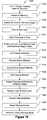
- FIG. 1illustrates an oblique view of a portion of a device according to one aspect of the present invention.
- FIG. 2illustrates a cross-sectional view of another portion of the device of FIG. 1 .
- FIG. 3illustrates a method according to another aspect of the present invention.
- FIG. 4illustrates a portion of the core region of a partially formed memory device according to a further aspect of the present invention.
- FIG. 5illustrates a method according to a still further aspect of the present invention.
- FIG. 6illustrates the memory stack of a SONOS memory device.
- FIG. 7illustrates the memory stack of a conventional floating gate memory device.
- FIG. 8is an illustration corresponding to a view along a portion of line AA′ of FIG. 4 after forming a dielectric layer over the core region.
- FIG. 9is an illustration corresponding to FIG. 8 after masking a space between word lines.
- FIG. 10is an illustration corresponding to FIG. 9 after etching.
- FIG. 11illustrates a method according to yet another aspect of the present invention.
- FIG. 12is an illustration corresponding to a view along a portion of line AA′ of FIG. 4 after forming a dielectric layer over the core region and polishing.
- FIG. 13is an illustration corresponding to a view along a portion of line AA′ of FIG. 4 after forming a thick dielectric layer over the core region.
- FIG. 14is an illustration corresponding to FIG. 13 after etching.
- FIG. 15illustrates a method according to a still further aspect of the present invention.
- the present inventioninvolves a process for fabricating virtual ground array flash memory devices, and in particular, a process for saliciding the word lines of such devices without saliciding the substrate between word lines.
- the deviceshave core and peripheral regions.
- the core regionincludes memory cells and the peripheral region includes low voltage gates, high voltage gates, and other input/output circuitry.
- the memory cellsinclude polysilicon or amorphous silicon control gates that are connected in continuous strips to form word lines.
- the drains and the sources of the memory cellsare connected, either in series or in parallel, to form bit lines.
- decoders and control circuitry in the peripheral regioneach memory cell can be addressed for programming, reading or erasing functions. Saliciding of word lines reduces the electrical response delay in performing these functions.
- FIGS. 1 and 2illustrate portions of the core region of a flash memory device 10 with salicided word lines according to one aspect of the present invention.
- the device illustratedhas a NOR structure, has buried bit lines, and is of SONOS type.
- the inventionencompasses devices with NAND structure, bit lines that are not buried, and floating gate memory cells.
- Word lines 20 of device 10are continuous strips patterned from a polysilicon or amorphous silicon layer. Word lines 20 overlay dielectric charge trapping layers that include oxide layer 14 , nitride layer 16 , and oxide layer 18 . Some of the word lines 20 are comparatively broadly spaced to provide room for bit line contacts 28 . Bit line contacts 28 generally include a metal, aluminum or copper, for example. In FIG. 2, bit line contacts 28 are illustrated as occurring once every eight word lines, however, other periods can be employed. Memory cells occur along word lines 20 between buried bit lines 26 . Buried bit lines 26 include doped regions of substrate 12 and serve as sources and drains for the memory cells. The bit lines are electrically isolated from each other by portions of substrate 12 with opposite doping from that of bit lines 26 (forming oppositely directed p-n junctions). Word lines 20 are salicided, but the substrate between word lines is essentially free of salicide.
- the memory cellscan be floating gate memory cells, although in such a case at least one of the charge trapping layers is conductive and does not form continuous strips along the word lines.
- the portions of substrate 12 between word lines 20are generally free from oxide islands, although these portions of the substrate are often covered by a relatively thin layer of spacer material or other material used for salicide protection as described more fully below.
- Oxide islandsare layers of dielectric material that are generally at least about 100 ⁇ thick, and typically at least about 500 ⁇ thick, such as formed by local oxidation of silicon (LOCOS) or shallow trench isolation (STI).
- LOCOSlocal oxidation of silicon
- STIshallow trench isolation
- Prior art memory devicescommonly have oxide islands formed in spaces between word lines. These islands are provided at locations where they facilitate maintaining electrical isolation of bit lines. For example, oxide islands may be placed between bit lines to protect portions of the substrate that serve to electrically isolate adjacent bit lines. Oxide islands are generally unnecessary in devices made according to processes of the present invention.
- FIG. 3provides a flow chart showing certain actions in a process 300 in accordance with another aspect of the invention.
- Process 300can be employed in producing memory device 10 of FIGS. 1 and 2.
- Act 302is setting the threshold voltage, V T , for the substrate and forming buried bit lines.
- the substrateis generally doped p-type while the bit lines are generally doped n-type.
- these doping stepscan take place after the multilayer charge trapping dielectric is formed.
- the substrate dopingcan be carried out with a blanket doping, whereas the bit line doping generally involves doping through a lithographically patterned resist mask.
- FIG. 4illustrates a semiconductor substrate 400 with buried bit lines 402 , such as could be produced by act 302 .
- Word linesare to be formed over the substrate and perpendicular to bit lines 402 .
- the spacing between word linesis generally fixed, although broader spacings are provided between some of the word lines to accommodate bit lines contacts at locations 404 .
- Act 304is forming the memory cell stack in at least the core region.
- the memory cell stackcan be either a SONOS type memory cell stack or a floating gate memory cell stack.
- Peripheral region gate stackscan be formed at the same time as the core memory cell stack, with portions of the core memory cell stack extending into the peripheral region. For example, it is common for at least an oxide layer and a poly layer to extend into the periphery.
- Act 306is patterning the poly layer in at least the core region to form word lines.
- the entire memory cell stackcan be patterned at this time, whereby the substrate between word lines is exposed.
- one or more layers of the memory cell stackcan be left in between word lines.
- Gates of the peripheral regioncan also be patterned at this time.
- a maskcan be provided to cover at least a portion of the substrate between word lines.
- such a maskgenerally covers at least the substrate between word lines that are broadly spaced to provide locations for bit line contacts.
- a dielectric layer of the memory cell stackcan later provide salicide protection for the substrate between word lines.
- a salicide protect layeris a layer of any material that can prevent the underlying substrate from becoming salicided.
- a salicide protect layercan include a spacer material and/or one or more other materials. The spacer material can be deposited over the substrate as part of a process of forming source and drain regions adjacent gates in the peripheral region.
- a maskis provided to limit the etching of spacer material, particularly in the space between broadly spaced word lines. Another option is to deposit extra spacer material, which can facilitate leaving spacer material in the spaces between word lines after a spacer etch.
- a further optionis to deposit a layer of dielectric or similar material solely to provide, or facilitate providing, a salicide protect layer.
- the tops of word linesare exposed without exposing the substrate between word lines.
- thiscan be accomplished with an ordinary etching process, either isotropic or anisotropic.
- Another option that can be used singularly or in combination with one or more etching processesis to remove at least a portion of a dielectric layer with a polishing process.
- Act 310is saliciding.
- a saliciding metalis deposited over the substrate by any suitable process. Rapid thermal annealing (RTA) is carried out under conditions wherein the saliciding metal reacts with silicon to form a metal silicide. Additional RTA can be employed to obtain the silicide in a desired phase.
- RTARapid thermal annealing
- the salicide protect layerprevents the substrate between word lines form becoming salicided. Therefore, essentially no silicide forms on the substrate between word lines.
- FIG. 5provides a flow chart of a more detailed example of a process 500 according to yet another aspect of the present invention.
- the sequencebegins with act 502 , forming a charge trapping dielectric stack over the core region of a substrate that includes a semiconductor.
- the semiconductoris generally silicon, but can be any suitable semiconductor, GaAs or InP for example.
- the charge trapping dielectric stackcan be the charge trapping portion of a SONOS memory cell stack.
- FIG. 6provides an example of a SONOS memory cell stack 600 .
- SONOS memory cell stack 600include a charge trapping dielectric 604 and a poly layer 606 formed over substrate 602 .
- the charge trapping dielectriccan be any dielectric layer or layers that are capable of or facilitate electron trapping.
- the charge trapping dielectrichas a layer with a lower barrier height than the layers sandwiching it (two layers with relatively higher barrier heights sandwiching a layer with a relatively lower barrier height).
- the oxide layershave a barrier height of about 3.1 eV whereas the nitride layer has a barrier height of about 2.1 eV. In this connection, a well is created in the middle layer.
- charge trapping dielectricsinclude an ONO trilayer dielectric, an oxide/nitride bilayer dielectric, a nitride/oxide bilayer dielectric, an oxide/tantalum oxide bilayer dielectric (SiO 2 /Ta 2 O 5 ), an oxide/tantalum oxide/oxide trilayer dielectric (SiO 2 /Ta 2 O 5 /SiO 2 ), an oxide/strontium titanate bilayer dielectric (SiO 2 /SrTiO 3 ), an oxide/barium strontium titanate bilayer dielectric (SiO 2 /BaSrTiO 2 ), an oxide/strontium titanate/oxide trilayer dielectric (SiO 2 /SrTiO 3 /SiO 2 ), an oxide/strontium titanate/barium strontium titanate trilayer dielectric (SiO 2 /SrTiO 3 /SiO 2 ), an oxide/strontium titanate/barium strontium
- SONOSis suggestive of an ONO layer
- the termencompasses nonvolatile memory devices containing any of the charge trapping dielectrics described above.
- a SONOS type nonvolatile memory devicecontains any dielectric layer or layers that are capable of or facilitate electron trapping, and does not require an ONO charge trapping dielectric.
- one or both of the silicon dioxide layerscan be a silicon-rich silicon dioxide layer.
- One or both of the silicon dioxide layerscan also be an oxygen-rich silicon dioxide layer.
- One or both of the silicon dioxide layerscan be a thermally grown or a deposited oxide.
- One or both of the silicon dioxide layerscan be nitrided oxide layers.
- a nitride layercan be a silicon-rich silicon nitride layer.
- the nitridecan also be a nitrogen-rich silicon nitride layer.
- the charge trapping dielectrichas a thickness from about 75 ⁇ to about 300 ⁇ . In another aspect of the invention, the charge trapping dielectric has a thickness from about 100 ⁇ to about 275 ⁇ . In a further aspect of the invention, the charge trapping dielectric has a thickness from about 110 ⁇ to about 250 ⁇ .
- the oxide layersindividually have thicknesses from about 50 ⁇ to about 150 ⁇ while the nitride layer has a thickness from about 20 ⁇ to about 80 ⁇ . In another aspect of the invention, the oxide layers individually have thicknesses from about 60 ⁇ to about 140 ⁇ while the nitride layer has a thickness from about 25 ⁇ to about 75 ⁇ . In a further aspect of the invention, the oxide layers individually have thicknesses from about 70 ⁇ to about 130 ⁇ while the nitride layer has a thickness from about 30 ⁇ to about 70 ⁇ .
- process 500is primarily concerned with forming a SONOS type memory device, the invention can also be employed to form floating gate memory devices. If a floating gate memory device is to be formed, act 502 , which involves forming the charge trapping layers of the memory cell stack, is postponed until after the threshold voltage for the substrate is set and buried bit lines are formed.
- FIG. 7provides an example of a stack 700 for floating gate memory cells.
- Gate oxide layer 704is formed over semiconductor substrate 702 .
- gate oxide layer 704is about 30 ⁇ to about 150 ⁇ thick.
- gate oxide layer 704is about 50 ⁇ to about 150 ⁇ thick.
- Gate oxidescan be formed by any suitable processes including chemical vapor deposition (CVD), dry oxidation, wet oxidation, or thermal oxidation.
- the gate oxide layer 704can be formed by dry oxidation at a temperature of about 1050° C., under an atmosphere containing 1 . 33 liters oxygen. 70 cc HCl and 12.6 liters argon.
- Floating gate layer 706is formed over gate oxide layer 704 .
- Floating gate layer 706generally contains polysilicon or amorphous silicon.
- Floating gate layer 706can be formed in any suitable manner.
- a phosphorus doped amorphous silicon layercan be deposited via CVD at 530° C., 400 mTorr, with 2000 sccm SiH 4 , 22 sccm helium, and 1% by weight PH 3 .
- floating gate layer 706has a thickness of about 400 ⁇ to about 1,200 ⁇ .
- floating gate layer 706has a thickness of about 500 ⁇ to about 1,000 ⁇ .
- floating gate layer 706has a thickness of about 700 ⁇ to about 900 ⁇ .
- a dielectric layer 708is formed over floating gate layer 706 .
- this dielectric layeris a multilayer dielectric such as an oxide/nitride/oxide (“ONO”) layer.
- the thicknessis typically about 120 ⁇ to about 400 ⁇ .
- an ONO layeris formed by successive formation of oxide, nitride and oxide layers.
- the ONO layerscan have any suitable thicknesses.
- the first or bottom oxide layercan be, for example, from about 40 ⁇ to about 60 ⁇ thick.
- the nitride layercan be, for example, about 60 ⁇ to about 100 ⁇ thick, or from about 70 ⁇ to about 90 ⁇ thick.
- the top oxide layercan be, for example, from about 20 ⁇ to about 80 ⁇ thick, or about 40 ⁇ to about 60 ⁇ thick.
- One or more of the oxide layerscan also form part of a peripheral region gate oxide.
- Dielectric layer 708can be formed by any suitable means.
- a bottom oxide layercan be formed using a CVD technique or grown using an oxidation technique.
- a bottom oxide layercan be formed at a temperature of about 750° C. and a pressure of 600 mTorr with a gas containing 20 sccm SiH 4 , 1200 sccm N 2 O, and a carrier gas.
- An oxide layercan also be formed by depositing then oxidizing TEOS.
- a nitride layercan also be deposited using CVD techniques. For example, nitride is deposited at a temperature of about 760° C.
- the second or top oxide layercan be formed in a manner similar to or different from that employed in forming the first oxide layer.
- a poly layer 710covers the charge trapping layers.
- Peripheral region gate stacksare commonly formed, at least in part, at the same time as the core memory cell stack. Two oxide thicknesses are often employed in the periphery, one for low voltage gates and another for high voltage gates.
- the gate oxide layers in the peripheryare typically thicker than in the core. For example, a gate oxide in the peripheral region can be about 130 ⁇ to about 400 ⁇ thick. Core and peripheral region gate oxides can be grown at the same time or at different times.
- the substrateis doped to set the threshold voltage (V T ) in act 504 .
- V Tthreshold voltage
- the substratecan be doped lightly (n ⁇ or p ⁇ ) or heavily (n+ or p+).
- suitable dopantsinclude one or more of arsenic, boron, and phosphorus.
- the dopingcan involve several layers or wells. Generally, the uppermost well is made p-type.
- boroncan be implanted to a dosage of about 1 ⁇ 10 11 atoms per cm 2 to about 1 ⁇ 10 13 atoms per cm 2 .
- the implantcan be carried out with an energy of about 80 kev to about 300 keV.
- Act 506is forming buried bit lines.
- Buried bit linesare formed by doping the substrate. Suitable dopants again include one or more of arsenic, boron, BF 2 + , antimony, indium, and phosphorus, although the dopant used to form the buried bit lines is of opposite type from that used to set the threshold voltage for the substrate.
- the bit linesare implanted to a dosage from about 1 ⁇ 10 14 to about 1 ⁇ 10 16 atoms/cm 2 .
- the bit linesare implanted to a dosage from about 5 ⁇ 10 14 to about 7 ⁇ 10 15 atoms/cm 2 .
- the bit linesare implanted to a dosage from about 1 ⁇ 10 15 to about 5 ⁇ 10 15 atoms/cm 2 .
- the bit linescan be implanted prior to setting the threshold voltage for the substrate.
- Act 508is forming a poly layer over at least the core region.
- the poly layercontains amorphous silicon or polysilicon.
- the poly layerhas a thickness of about 500 ⁇ to about 6000 ⁇ .
- the poly layerhas a thickness of about 750 ⁇ to about 3000 ⁇ .
- the poly layerhas a thickness of about 1,000 ⁇ to about 1,500 ⁇ .
- the poly layercan be formed by any suitable means, including the type of means used to form the floating gate layer of a floating gate memory cell stack.
- the poly layergenerally extends over the peripheral region. Any core region memory cell stack layers that are not wanted in the peripheral region can be selectively formed in the core region or selectively etched from the peripheral region with one or more lithographic masks.
- Act 510is doping the poly layer in at least the core region, Any suitable dopant can be used, arsenic for example.
- the poly layeris doped with about 1 ⁇ 10 11 to about 1 ⁇ 10 16 atoms/cm 2 .
- the poly layeris doped with about 1 ⁇ 10 13 to about 5 ⁇ 10 15 atoms/cm 2 .
- the poly layeris doped with about 3 ⁇ 10 14 to about 3 ⁇ 10 15 atoms/cm 2 .
- the peripheral regionis masked while the poly layer is being doped in the core region.
- act 508 and act 510can be performed simultaneously. In these instances, in situ doping formation techniques may be employed.
- Act 512which takes place after doping the poly layer in the core region, is patterning the core memory cells and peripheral region gates. Patterning can be carried out with any suitable method, including, for example, a lithographic process. Patterning the core memory cells involves patterning at least the poly layer. The patterning divides the poly layer of the core region into spaced apart word lines. In one aspect of the invention, patterning provides a spacing between word lines, except where contacts are placed, from about 0.05 ⁇ m to about 1.5 ⁇ m. In another aspect of the invention, the spacing between word lines is from about 0.1 ⁇ m to about 1 ⁇ m. In a further aspect of the invention, the spacing between word lines is from about 0. 15 ⁇ m to about 0.75 ⁇ m. The widths of the word lines are comparable to the spaces between word lines.
- the word line spacingis increased where bit line contacts are to be provided. In one aspect of the invention, the spacing is increased by a factor of about 1.5 to about 4. In a further aspect of the invention, the spacing is increased by a factor of about 2 to about 3.
- Acts 514 , 516 , 520 , and 522provide source and drain regions adjacent gates in the peripheral region. During these optional steps, n-type and p-type transistors are masked and implanted separately. The core is generally masked at least during acts 514 and 522 , which involve doping.
- Optional act 514is an optional self aligned LDD implant. This implant provides a dosage of about 1 ⁇ 10 11 atoms/cm 2 to about 1 ⁇ 10 13 atoms/cm 2 at an energy of about 20 keV to about 80 keV. Suitable dopants can include, for example, arsenic, boron, or phosphorus. Act 514 is optional to the extent that an LDD doping for peripheral region gates can be provided when the poly layer is doped in act 510 (acts 510 and 514 performed simultaneously).
- Optional act 516is depositing a spacer material. Any suitable material can be used, including a nitride and/or an oxide, for example. An oxide layer can be formed by depositing then oxidizing TEOS. Using CVD techniques, a nitride layer can also be deposited. Any masks are normally removed prior to depositing the spacer material, whereby the spacer material generally deposits directly over and between the word lines of the core region.
- Optional act 518is providing a mask to protect the substrate between word lines during spacer etching, at least between word lines where the substrate would otherwise be exposed due to broad word line spacing that provides for bit line contacts.
- a maskcan alternatively be provided for any of the dielectric etching processes, including one or more etching processes employed to pattern the memory cells in the core region.
- the maskpreserves spacer material, or other dielectric material, over the substrate between word lines, whereby some dielectric remains after etching and protects the substrate against saliciding.
- the maskneed not be provided throughout an etching process, or through every etching process.
- a subsequent etching processcan expose the substrate adjacent gates in the peripheral region without exposing the substrate between word lines in the core region.
- Optional act 520is etching and can be carried out with any suitable process. Etching leaves a layer of spacer material to the sides of the peripheral region gates while exposing the source and drain regions for the peripheral gates.
- the etching processis usually an anisotropic etching process, such as reactive ion etching. Choice of a suitable process and reagents depends on the spacer material. Reactive ion etching can be carried out with CF 4 , for example. Wet etching can be carried out with an acid, a base, or a solvent. Acids that can be employed include hydrofluoric acid, hydrobromic acid, nitric acid, phosphoric acid or acetic acid.
- Bases that can be employedinclude hydroxides such as sodium hydroxide, ammonium hydroxide, and potassium hydroxide.
- Solventscan be polar, such as water, or non-polar, such as xylene or cellusolve, or of intermediate polarity, such as alcohols including methanol.
- Act 522is doping to provide source and drain regions adjacent gates in the periphery. The spacers limit the concentration of dopant immediately adjacent the gates. N-type and p-type gates are doped separately. In one aspect of the invention, the dopants are implanted to a dosage from about 1 ⁇ 10 14 to about 1 ⁇ 10 16 atoms/cm 2 .
- the dopantsare implanted to a dosage from about 5 ⁇ 10 14 to about 7 ⁇ 10 15 atoms/cm 2 . In a further aspect of the invention, the dopants are implanted to a dosage from about 1 ⁇ 10 15 to about 5 ⁇ 10 15 atoms/cm 2 .
- Act 524which is carried out prior to saliciding, is removing any material on the tops of the word lines, particularly spacer material, while leaving a protective layer over the substrate between word lines in the core region.
- the peripheryis also masked.
- a spacer or dielectric material over the word linescan be removed by chemical, mechanical, or combined chemical and mechanical means.
- Chemical removalincludes wet etching. Additional examples of chemical removal include plasma and reactive ion etching.
- the plasmacan be of oxygen, fluorine, chlorine, hydrogen, or a combination of these, optionally with other gases. Reactive ion etching can be done with oxygen, for example.
- Combined chemical and mechanical meansinclude chemical mechanical polishing (CMP).
- CMPuses a material, often referred to as a slurry, that does not rapidly dissolve the layer being removed, but modifies its chemical bonding sufficiently to facilitate mechanical removal with a polishing pad. Material can also be removed by purely mechanical means. A polishing pad attached to a rigid flat surface can be moved against the upper layer to gradually remove an amount of material appropriate to expose the tops of the word lines.
- Acts 526 , 528 , and 530relate to the saliciding process. This process forms a silicide on exposed silicon, including at least the word lines of the core region.
- the silicideis also formed in the source and drain regions of the periphery.
- a silicideis a compound of Si and a metal. Any suitable metal can be employed, including metals of the Group IVA, VA, and VIII. Specific examples include Ti, Ni, or Co, forming compounds such as TiSi 2 , NiSi, and CoSi 2 .
- metalis deposited over the surface.
- the metalcan be deposited by any suitable means, including, for example, evaporation, sputtering, and CVD.
- evaporationa metal film is deposited by condensation of a vapor on the substrate, which is maintained at a lower temperature than the vapor.
- the metalcan be vaporized by any suitable method, including, for example, resistive heating, inductive heating, laser bombardment, or laser heating.
- the metal to be depositedis bombarded by energetic ions to free some atoms. These atoms are condensed on the substrate to form the film.
- the metalis produced by one or more reactions occurring either in the vapor phase or at the surface of the substrate. The reactions are generally induced by heat, which causes either a decomposition of the metal containing compound or reaction between the different species. Metal organic compounds are useful in CVD processes.
- silicideis formed in act 528 by RTA.
- RTAis employed because it induces chemical reactions and phase changes while avoiding prolonged heating of the substrate that could cause undo diffusion of the metal or dopants.
- RTAis generally accomplished with lasers, heat lamps, such as arc or tungsten-halogen lamps, although other suitable apparatus can be employed, including an electrically heated bell jar and in some cases, a furnace. The temperature depends on, among other factors, the type of silicide being formed.
- Annealing of titanium silicideoften involves two RTA steps.
- the first RTAis at a temperature from about 500 to about 700° C. and results in the formation of the relatively high resistivity C 49 TiSi 2 phase.
- RTAat 650° C. for 30 seconds can be employed.
- a selective etchcan be used to remove un-reacted metal on the sidewall spacer and isolate gates from the source/drain regions.
- a second RTA at a temperature from about 700 and about 900° C.transforms the relatively high resistivity C 49 TiSi 2 phase to the relatively low resistivity phase C 54 TiSi x .
- the atmosphere (N 2 , level of vacuum, etc.) and impuritiescan affect the competing kinetics and vary the optimum anneal time and temperature.
- CoSi 2is also commonly formed with two RTA steps.
- TiN cappingcan be employed to prevent oxidation of Co and provide a smooth film.
- a Co filmcan be sputter-deposited, followed by TiN film deposition while maintaining a vacuum.
- the TiN capis etched off using ammonium hydroxide solution.
- the un-reacted Co layer on SiO 2 , or other spacer material,is selectively etched off using hydrochloric acid solution.
- a second RTAconverts CoSi to CoSi 2 .
- Act 530removes any un-reacted metal that could form unwanted compounds in later processing steps.
- Un-reacted metalcan be removed by any suitable means. Generally, the metal is removed by washing with an acid solution. For example, a solution of hydrochloric and/or nitric acid can be employed. Although not shown, further processing is performed to complete the fabrication of the flash memory device.
- FIGS. 8 to 10schematically illustrate an example of the foregoing process.
- FIG. 8illustrates a potion of the core wherein memory cells 804 and a contact location 808 in substrate 804 are coated with a spacer material 806 .
- the viewcorresponds to a portion of the cross section along line AA′ in FIG. 4 .
- FIG. 9illustrates the formation of a mask 810 over contact location 808 .
- FIG. 10illustrates the result of an etch carried out with mask 810 in place. The spacer material over contact location 808 is preserved while the tops of memory cells 804 are exposed.
- FIG. 11is a flow chart of a process 1100 according to another aspect of the present invention.
- Process 1100has many steps that are similar to process 500 , including, forming a charge trapping stack in the core, implanting to adjust V T , implanting bit lines, forming a poly layer, doping the poly layer, masking and etching the memory cells and the peripheral region gates, LDD implanting the periphery, depositing spacer material, etching the spacer material, forming sources and drains adjacent peripheral region gates, depositing saliciding metal, RTA, and removing excess saliciding metal. Differences lie in acts 1118 and 1120 . In act 1118 , a dielectric, spacer, or similar material is polished off from the core region.
- the materialcan be a spacer material or a material deposited to provide salicide protection for the substrate between word lines.
- the polishingis usually carried out to expose the tops of the word lines, but the tops of the word lines can also be exposed with a combination of etching and polishing.
- the polishing stepcan take place after implanting sources and drains in the periphery. Additional salicide protection material can be deposited after implanting the sources and drains. Examples of polishing processes include mechanical polishing and chemical mechanical polishing, which were discussed previously.
- Act 1120is a spacer etch similar to that employed in process 500 .
- the coreis optionally masked.
- the corecan be masked throughout the spacer etch if the polishing process exposes the tops of the word lines. Saliciding takes place after the tops of the core memory cells have been exposed.
- FIG. 12illustrates a potential result of the polishing process.
- the polishingoccurs substantially along a plane, whereby the tops of word lines 1204 are exposed, but dielectric material 1206 substantially fills the areas between word lines 1204 and specifically covers contact location 1208 , whereby core word lines 1204 can be salicided without saliciding contact location 1208 .
- FIG. 15is a flow chart of a process 1500 according to yet another aspect of the present invention.
- Process 1500has many steps that are similar to process 500 , including, forming a charge trapping stack in the core, implanting to adjust V T , implanting bit lines, forming a poly layer, doping the poly layer, masking and etching the memory cells and the peripheral region gates, LDD implanting the periphery, depositing spacer material, forming sources and drains adjacent peripheral region gates, depositing saliciding metal, RTA, and removing excess saliciding metal.
- differenceslie in one or more of acts 1518 , 1520 and 1524 .
- act 1518extra spacer material, a dielectric, or similar material, is deposited over at least the core. Act 1518 can optionally be postponed until after peripheral region sources and drains are formed in act 1522 .
- a dielectric or similar materialcan be an oxide, a nitride, or other material that can be etched without substantially etching polysilicon.
- the extra materialis deposited to a thickness from about 0.25 to about 5 times that of the memory cell stack. In another aspect of the invention, it is deposited to a thickness from about 0.5 to about 2.5 times that of the memory cell stack. In a further aspect of the invention, it is deposited to a thickness from about 1 to about 1.5 that of the memory cell stack.
- the extra materialcan be etched as part of act 1520 , the spacer etch, and/or as part of act 1524 , exposing the tops of the word lines. Isotropic and/or anisotropic etches can be employed. Material can also be removed by polishing.
- FIGS. 13 and 14illustrate the effect of depositing extra material.
- FIG. 13illustrates a thick dielectric layer 1306 covering word lines 1304 and contact location 1308 .
- Dielectric layer 1306can include a plurality of dielectric layers.
- the thick layer deposition, and the extended etching process that follows,have the effect of smoothing over topographical features created by the word lines 1304 on substrate 1302 .
- etchingas illustrated in FIG. 14, a relatively level dielectric surface is formed and the tops of word lines 1304 can be exposed without exposing contact locations 1308 .
Landscapes
- Engineering & Computer Science (AREA)
- Physics & Mathematics (AREA)
- Condensed Matter Physics & Semiconductors (AREA)
- General Physics & Mathematics (AREA)
- Manufacturing & Machinery (AREA)
- Computer Hardware Design (AREA)
- Microelectronics & Electronic Packaging (AREA)
- Power Engineering (AREA)
- Semiconductor Memories (AREA)
Abstract
Description
Claims (30)
Priority Applications (1)
| Application Number | Priority Date | Filing Date | Title |
|---|---|---|---|
| US09/968,456US6645801B1 (en) | 2001-10-01 | 2001-10-01 | Salicided gate for virtual ground arrays |
Applications Claiming Priority (1)
| Application Number | Priority Date | Filing Date | Title |
|---|---|---|---|
| US09/968,456US6645801B1 (en) | 2001-10-01 | 2001-10-01 | Salicided gate for virtual ground arrays |
Publications (1)
| Publication Number | Publication Date |
|---|---|
| US6645801B1true US6645801B1 (en) | 2003-11-11 |
Family
ID=29401940
Family Applications (1)
| Application Number | Title | Priority Date | Filing Date |
|---|---|---|---|
| US09/968,456Expired - LifetimeUS6645801B1 (en) | 2001-10-01 | 2001-10-01 | Salicided gate for virtual ground arrays |
Country Status (1)
| Country | Link |
|---|---|
| US (1) | US6645801B1 (en) |
Cited By (37)
| Publication number | Priority date | Publication date | Assignee | Title |
|---|---|---|---|---|
| US20040043622A1 (en)* | 2002-09-04 | 2004-03-04 | Chien-Wei Chen | Method for preventing hole and electron movement in NROM devices |
| US6744105B1 (en)* | 2003-03-05 | 2004-06-01 | Advanced Micro Devices, Inc. | Memory array having shallow bit line with silicide contact portion and method of formation |
| US20040108540A1 (en)* | 2002-12-09 | 2004-06-10 | Nec Electronics Corporation | Nonvolatile semiconductor memory device and method for manufacturing same |
| US6773988B1 (en)* | 2002-09-13 | 2004-08-10 | Advanced Micro Devices, Inc. | Memory wordline spacer |
| US6917544B2 (en) | 2002-07-10 | 2005-07-12 | Saifun Semiconductors Ltd. | Multiple use memory chip |
| US20070010062A1 (en)* | 2005-07-07 | 2007-01-11 | Texas Instruments, Incorporated | Method to obtain fully silicided poly gate |
| US20070105306A1 (en)* | 2005-11-04 | 2007-05-10 | Freescale Semiconductor, Inc. | Nanocrystal bitcell process integration for high density application |
| US7221138B2 (en) | 2005-09-27 | 2007-05-22 | Saifun Semiconductors Ltd | Method and apparatus for measuring charge pump output current |
| US7317633B2 (en) | 2004-07-06 | 2008-01-08 | Saifun Semiconductors Ltd | Protection of NROM devices from charge damage |
| US20080025084A1 (en)* | 2005-09-08 | 2008-01-31 | Rustom Irani | High aspect ration bitline oxides |
| US7352627B2 (en) | 2006-01-03 | 2008-04-01 | Saifon Semiconductors Ltd. | Method, system, and circuit for operating a non-volatile memory array |
| US7369440B2 (en) | 2005-01-19 | 2008-05-06 | Saifun Semiconductors Ltd. | Method, circuit and systems for erasing one or more non-volatile memory cells |
| US20080153269A1 (en)* | 2006-12-26 | 2008-06-26 | Cinti Chen | Thin oxide dummy tiling as charge protection |
| US7405969B2 (en) | 1997-08-01 | 2008-07-29 | Saifun Semiconductors Ltd. | Non-volatile memory cell and non-volatile memory devices |
| US7420848B2 (en) | 2002-01-31 | 2008-09-02 | Saifun Semiconductors Ltd. | Method, system, and circuit for operating a non-volatile memory array |
| US7457183B2 (en) | 2003-09-16 | 2008-11-25 | Saifun Semiconductors Ltd. | Operating array cells with matched reference cells |
| US7466594B2 (en) | 2004-08-12 | 2008-12-16 | Saifun Semiconductors Ltd. | Dynamic matching of signal path and reference path for sensing |
| EP1763080A3 (en)* | 2005-09-08 | 2009-01-14 | Saifun Semiconductors Ltd. | Non-volatile memory device |
| JPWO2007000808A1 (en)* | 2005-06-28 | 2009-01-22 | スパンション エルエルシー | Semiconductor device and manufacturing method thereof |
| US7512009B2 (en) | 2001-04-05 | 2009-03-31 | Saifun Semiconductors Ltd. | Method for programming a reference cell |
| US7518908B2 (en) | 2001-01-18 | 2009-04-14 | Saifun Semiconductors Ltd. | EEPROM array and method for operation thereof |
| US7532529B2 (en) | 2004-03-29 | 2009-05-12 | Saifun Semiconductors Ltd. | Apparatus and methods for multi-level sensing in a memory array |
| US7605579B2 (en) | 2006-09-18 | 2009-10-20 | Saifun Semiconductors Ltd. | Measuring and controlling current consumption and output current of charge pumps |
| US7638835B2 (en) | 2006-02-28 | 2009-12-29 | Saifun Semiconductors Ltd. | Double density NROM with nitride strips (DDNS) |
| US7638850B2 (en) | 2004-10-14 | 2009-12-29 | Saifun Semiconductors Ltd. | Non-volatile memory structure and method of fabrication |
| US7668017B2 (en) | 2005-08-17 | 2010-02-23 | Saifun Semiconductors Ltd. | Method of erasing non-volatile memory cells |
| US7675782B2 (en) | 2002-10-29 | 2010-03-09 | Saifun Semiconductors Ltd. | Method, system and circuit for programming a non-volatile memory array |
| US7692236B1 (en)* | 2005-02-15 | 2010-04-06 | Spansion Llc | Multiple dual bit memory integrated circuit system |
| US7692961B2 (en) | 2006-02-21 | 2010-04-06 | Saifun Semiconductors Ltd. | Method, circuit and device for disturb-control of programming nonvolatile memory cells by hot-hole injection (HHI) and by channel hot-electron (CHE) injection |
| US7701779B2 (en) | 2006-04-27 | 2010-04-20 | Sajfun Semiconductors Ltd. | Method for programming a reference cell |
| US7743230B2 (en) | 2003-01-31 | 2010-06-22 | Saifun Semiconductors Ltd. | Memory array programming circuit and a method for using the circuit |
| US7760554B2 (en) | 2006-02-21 | 2010-07-20 | Saifun Semiconductors Ltd. | NROM non-volatile memory and mode of operation |
| US7786512B2 (en) | 2005-07-18 | 2010-08-31 | Saifun Semiconductors Ltd. | Dense non-volatile memory array and method of fabrication |
| US7808818B2 (en) | 2006-01-12 | 2010-10-05 | Saifun Semiconductors Ltd. | Secondary injection for NROM |
| US8053812B2 (en) | 2005-03-17 | 2011-11-08 | Spansion Israel Ltd | Contact in planar NROM technology |
| US8253452B2 (en) | 2006-02-21 | 2012-08-28 | Spansion Israel Ltd | Circuit and method for powering up an integrated circuit and an integrated circuit utilizing same |
| US10850595B2 (en)* | 2018-03-07 | 2020-12-01 | Magna Electronics Inc. | Vehicular sensing system with attenuation of reflected-refracted light off of precipitation using light polarization |
Citations (18)
| Publication number | Priority date | Publication date | Assignee | Title |
|---|---|---|---|---|
| US4173766A (en) | 1977-09-16 | 1979-11-06 | Fairchild Camera And Instrument Corporation | Insulated gate field-effect transistor read-only memory cell |
| US5168334A (en) | 1987-07-31 | 1992-12-01 | Texas Instruments, Incorporated | Non-volatile semiconductor memory |
| US5284784A (en) | 1991-10-02 | 1994-02-08 | National Semiconductor Corporation | Buried bit-line source-side injection flash memory cell |
| US5349221A (en) | 1991-10-25 | 1994-09-20 | Rohm Co., Ltd. | Semiconductor memory device and method of reading out information for the same |
| US5717635A (en) | 1996-08-27 | 1998-02-10 | International Business Machines Corporation | High density EEPROM for solid state file |
| US5768192A (en) | 1996-07-23 | 1998-06-16 | Saifun Semiconductors, Ltd. | Non-volatile semiconductor memory cell utilizing asymmetrical charge trapping |
| US5966603A (en) | 1997-06-11 | 1999-10-12 | Saifun Semiconductors Ltd. | NROM fabrication method with a periphery portion |
| US5972751A (en) | 1998-08-28 | 1999-10-26 | Advanced Micro Devices, Inc. | Methods and arrangements for introducing nitrogen into a tunnel oxide in a non-volatile semiconductor memory device |
| US6001689A (en) | 1998-01-16 | 1999-12-14 | Advanced Micro Devices, Inc. | Process for fabricating a flash memory with dual function control lines |
| US6023085A (en) | 1997-12-18 | 2000-02-08 | Advanced Micro Devices, Inc. | Core cell structure and corresponding process for NAND-type high performance flash memory device |
| US6030871A (en) | 1998-05-05 | 2000-02-29 | Saifun Semiconductors Ltd. | Process for producing two bit ROM cell utilizing angled implant |
| US6074915A (en) | 1998-08-17 | 2000-06-13 | Taiwan Semiconductor Manufacturing Company | Method of making embedded flash memory with salicide and sac structure |
| US6130453A (en) | 1999-01-04 | 2000-10-10 | International Business Machines Corporation | Flash memory structure with floating gate in vertical trench |
| US6143608A (en) | 1999-03-31 | 2000-11-07 | Advanced Micro Devices, Inc. | Barrier layer decreases nitrogen contamination of peripheral gate regions during tunnel oxide nitridation |
| US6153471A (en) | 1999-03-29 | 2000-11-28 | United Semiconductor Corp. | Method of fabricating flash memory |
| US6153467A (en) | 1998-06-03 | 2000-11-28 | Texas Instruments - Acer Incorporated | Method of fabricating high density buried bit line flash EEPROM memory cell with a shallow trench floating gate |
| US6157575A (en) | 1998-03-26 | 2000-12-05 | Samsung Electronics Co., Ltd | Nonvolatile memory device and operating method thereof |
| US6159795A (en) | 1998-07-02 | 2000-12-12 | Advanced Micro Devices, Inc. | Low voltage junction and high voltage junction optimization for flash memory |
- 2001
- 2001-10-01USUS09/968,456patent/US6645801B1/ennot_activeExpired - Lifetime
Patent Citations (18)
| Publication number | Priority date | Publication date | Assignee | Title |
|---|---|---|---|---|
| US4173766A (en) | 1977-09-16 | 1979-11-06 | Fairchild Camera And Instrument Corporation | Insulated gate field-effect transistor read-only memory cell |
| US5168334A (en) | 1987-07-31 | 1992-12-01 | Texas Instruments, Incorporated | Non-volatile semiconductor memory |
| US5284784A (en) | 1991-10-02 | 1994-02-08 | National Semiconductor Corporation | Buried bit-line source-side injection flash memory cell |
| US5349221A (en) | 1991-10-25 | 1994-09-20 | Rohm Co., Ltd. | Semiconductor memory device and method of reading out information for the same |
| US5768192A (en) | 1996-07-23 | 1998-06-16 | Saifun Semiconductors, Ltd. | Non-volatile semiconductor memory cell utilizing asymmetrical charge trapping |
| US5717635A (en) | 1996-08-27 | 1998-02-10 | International Business Machines Corporation | High density EEPROM for solid state file |
| US5966603A (en) | 1997-06-11 | 1999-10-12 | Saifun Semiconductors Ltd. | NROM fabrication method with a periphery portion |
| US6023085A (en) | 1997-12-18 | 2000-02-08 | Advanced Micro Devices, Inc. | Core cell structure and corresponding process for NAND-type high performance flash memory device |
| US6001689A (en) | 1998-01-16 | 1999-12-14 | Advanced Micro Devices, Inc. | Process for fabricating a flash memory with dual function control lines |
| US6157575A (en) | 1998-03-26 | 2000-12-05 | Samsung Electronics Co., Ltd | Nonvolatile memory device and operating method thereof |
| US6030871A (en) | 1998-05-05 | 2000-02-29 | Saifun Semiconductors Ltd. | Process for producing two bit ROM cell utilizing angled implant |
| US6153467A (en) | 1998-06-03 | 2000-11-28 | Texas Instruments - Acer Incorporated | Method of fabricating high density buried bit line flash EEPROM memory cell with a shallow trench floating gate |
| US6159795A (en) | 1998-07-02 | 2000-12-12 | Advanced Micro Devices, Inc. | Low voltage junction and high voltage junction optimization for flash memory |
| US6074915A (en) | 1998-08-17 | 2000-06-13 | Taiwan Semiconductor Manufacturing Company | Method of making embedded flash memory with salicide and sac structure |
| US5972751A (en) | 1998-08-28 | 1999-10-26 | Advanced Micro Devices, Inc. | Methods and arrangements for introducing nitrogen into a tunnel oxide in a non-volatile semiconductor memory device |
| US6130453A (en) | 1999-01-04 | 2000-10-10 | International Business Machines Corporation | Flash memory structure with floating gate in vertical trench |
| US6153471A (en) | 1999-03-29 | 2000-11-28 | United Semiconductor Corp. | Method of fabricating flash memory |
| US6143608A (en) | 1999-03-31 | 2000-11-07 | Advanced Micro Devices, Inc. | Barrier layer decreases nitrogen contamination of peripheral gate regions during tunnel oxide nitridation |
Non-Patent Citations (3)
| Title |
|---|
| "A True Single-Transistor Oxide-Nitride-Oxide EEPROM Device," T.Y. Chan, et al., IEEE Electron Device Letters, vol. EDL 8, No. 3, Mar. 1987. |
| "An Electrically Alterable Nonvolatile Memory Cell Using a Floating-Gate Structure," Daniel C. Guterman, et al., IEEE Transactions on Electron Devices, vol. ED-26, No. 4, Apr. 1979. |
| "NROM: A Novel Localized Trapping, 2-Bit Nonvolatile Memory Cell," Boaz Eitan, et al., IEEE Electron Device Letters, vol. 21, No. 11 Nov. 2000. |
Cited By (46)
| Publication number | Priority date | Publication date | Assignee | Title |
|---|---|---|---|---|
| US7405969B2 (en) | 1997-08-01 | 2008-07-29 | Saifun Semiconductors Ltd. | Non-volatile memory cell and non-volatile memory devices |
| US7518908B2 (en) | 2001-01-18 | 2009-04-14 | Saifun Semiconductors Ltd. | EEPROM array and method for operation thereof |
| US7512009B2 (en) | 2001-04-05 | 2009-03-31 | Saifun Semiconductors Ltd. | Method for programming a reference cell |
| US7420848B2 (en) | 2002-01-31 | 2008-09-02 | Saifun Semiconductors Ltd. | Method, system, and circuit for operating a non-volatile memory array |
| US7738304B2 (en) | 2002-07-10 | 2010-06-15 | Saifun Semiconductors Ltd. | Multiple use memory chip |
| US6917544B2 (en) | 2002-07-10 | 2005-07-12 | Saifun Semiconductors Ltd. | Multiple use memory chip |
| US6784483B2 (en)* | 2002-09-04 | 2004-08-31 | Macronix International Co., Ltd. | Method for preventing hole and electron movement in NROM devices |
| US20040043622A1 (en)* | 2002-09-04 | 2004-03-04 | Chien-Wei Chen | Method for preventing hole and electron movement in NROM devices |
| US6773988B1 (en)* | 2002-09-13 | 2004-08-10 | Advanced Micro Devices, Inc. | Memory wordline spacer |
| US7675782B2 (en) | 2002-10-29 | 2010-03-09 | Saifun Semiconductors Ltd. | Method, system and circuit for programming a non-volatile memory array |
| US6914293B2 (en)* | 2002-12-09 | 2005-07-05 | Nec Electronics Corporation | Nonvolatile semiconductor memory device and method for manufacturing same |
| US20050214996A1 (en)* | 2002-12-09 | 2005-09-29 | Nec Electronics Corporation | Method of manufacturing a nonvolatile semiconductor memory device |
| US20040108540A1 (en)* | 2002-12-09 | 2004-06-10 | Nec Electronics Corporation | Nonvolatile semiconductor memory device and method for manufacturing same |
| US7743230B2 (en) | 2003-01-31 | 2010-06-22 | Saifun Semiconductors Ltd. | Memory array programming circuit and a method for using the circuit |
| US6744105B1 (en)* | 2003-03-05 | 2004-06-01 | Advanced Micro Devices, Inc. | Memory array having shallow bit line with silicide contact portion and method of formation |
| US7457183B2 (en) | 2003-09-16 | 2008-11-25 | Saifun Semiconductors Ltd. | Operating array cells with matched reference cells |
| US7532529B2 (en) | 2004-03-29 | 2009-05-12 | Saifun Semiconductors Ltd. | Apparatus and methods for multi-level sensing in a memory array |
| US7317633B2 (en) | 2004-07-06 | 2008-01-08 | Saifun Semiconductors Ltd | Protection of NROM devices from charge damage |
| US7466594B2 (en) | 2004-08-12 | 2008-12-16 | Saifun Semiconductors Ltd. | Dynamic matching of signal path and reference path for sensing |
| US7964459B2 (en) | 2004-10-14 | 2011-06-21 | Spansion Israel Ltd. | Non-volatile memory structure and method of fabrication |
| US7638850B2 (en) | 2004-10-14 | 2009-12-29 | Saifun Semiconductors Ltd. | Non-volatile memory structure and method of fabrication |
| US7369440B2 (en) | 2005-01-19 | 2008-05-06 | Saifun Semiconductors Ltd. | Method, circuit and systems for erasing one or more non-volatile memory cells |
| US7468926B2 (en) | 2005-01-19 | 2008-12-23 | Saifun Semiconductors Ltd. | Partial erase verify |
| US7692236B1 (en)* | 2005-02-15 | 2010-04-06 | Spansion Llc | Multiple dual bit memory integrated circuit system |
| US8053812B2 (en) | 2005-03-17 | 2011-11-08 | Spansion Israel Ltd | Contact in planar NROM technology |
| JPWO2007000808A1 (en)* | 2005-06-28 | 2009-01-22 | スパンション エルエルシー | Semiconductor device and manufacturing method thereof |
| US7498264B2 (en) | 2005-07-07 | 2009-03-03 | Texas Instruments Incorporated | Method to obtain fully silicided poly gate |
| US20070010062A1 (en)* | 2005-07-07 | 2007-01-11 | Texas Instruments, Incorporated | Method to obtain fully silicided poly gate |
| US7786512B2 (en) | 2005-07-18 | 2010-08-31 | Saifun Semiconductors Ltd. | Dense non-volatile memory array and method of fabrication |
| US7668017B2 (en) | 2005-08-17 | 2010-02-23 | Saifun Semiconductors Ltd. | Method of erasing non-volatile memory cells |
| US20080025084A1 (en)* | 2005-09-08 | 2008-01-31 | Rustom Irani | High aspect ration bitline oxides |
| EP1763080A3 (en)* | 2005-09-08 | 2009-01-14 | Saifun Semiconductors Ltd. | Non-volatile memory device |
| US7221138B2 (en) | 2005-09-27 | 2007-05-22 | Saifun Semiconductors Ltd | Method and apparatus for measuring charge pump output current |
| US20070105306A1 (en)* | 2005-11-04 | 2007-05-10 | Freescale Semiconductor, Inc. | Nanocrystal bitcell process integration for high density application |
| US7491600B2 (en) | 2005-11-04 | 2009-02-17 | Freescale Semiconductor, Inc. | Nanocrystal bitcell process integration for high density application |
| US7352627B2 (en) | 2006-01-03 | 2008-04-01 | Saifon Semiconductors Ltd. | Method, system, and circuit for operating a non-volatile memory array |
| US7808818B2 (en) | 2006-01-12 | 2010-10-05 | Saifun Semiconductors Ltd. | Secondary injection for NROM |
| US7692961B2 (en) | 2006-02-21 | 2010-04-06 | Saifun Semiconductors Ltd. | Method, circuit and device for disturb-control of programming nonvolatile memory cells by hot-hole injection (HHI) and by channel hot-electron (CHE) injection |
| US7760554B2 (en) | 2006-02-21 | 2010-07-20 | Saifun Semiconductors Ltd. | NROM non-volatile memory and mode of operation |
| US8253452B2 (en) | 2006-02-21 | 2012-08-28 | Spansion Israel Ltd | Circuit and method for powering up an integrated circuit and an integrated circuit utilizing same |
| US7638835B2 (en) | 2006-02-28 | 2009-12-29 | Saifun Semiconductors Ltd. | Double density NROM with nitride strips (DDNS) |
| US7701779B2 (en) | 2006-04-27 | 2010-04-20 | Sajfun Semiconductors Ltd. | Method for programming a reference cell |
| US7605579B2 (en) | 2006-09-18 | 2009-10-20 | Saifun Semiconductors Ltd. | Measuring and controlling current consumption and output current of charge pumps |
| US20080153269A1 (en)* | 2006-12-26 | 2008-06-26 | Cinti Chen | Thin oxide dummy tiling as charge protection |
| US7977218B2 (en)* | 2006-12-26 | 2011-07-12 | Spansion Llc | Thin oxide dummy tiling as charge protection |
| US10850595B2 (en)* | 2018-03-07 | 2020-12-01 | Magna Electronics Inc. | Vehicular sensing system with attenuation of reflected-refracted light off of precipitation using light polarization |
Similar Documents
| Publication | Publication Date | Title |
|---|---|---|
| US6645801B1 (en) | Salicided gate for virtual ground arrays | |
| US6566194B1 (en) | Salicided gate for virtual ground arrays | |
| US6074915A (en) | Method of making embedded flash memory with salicide and sac structure | |
| US8076708B2 (en) | Structures for and method of silicide formation on memory array and peripheral logic devices | |
| US4931411A (en) | Integrated circuit process with TiN-gate transistor | |
| US6461905B1 (en) | Dummy gate process to reduce the Vss resistance of flash products | |
| US6100559A (en) | Multipurpose graded silicon oxynitride cap layer | |
| US5744395A (en) | Low resistance, self-aligned, titanium silicide structures, using a single rapid thermal anneal procedure | |
| US7410869B2 (en) | Method of manufacturing a semiconductor device | |
| KR100469129B1 (en) | Non-volatile memory device and Method of manufacturing the same | |
| US4814854A (en) | Integrated circuit device and process with tin-gate transistor | |
| EP0528564A2 (en) | Self-aligned stacked gate EPROM cell using tantalum oxide control gate dielectric | |
| US6787419B2 (en) | Method of forming an embedded memory including forming three silicon or polysilicon layers | |
| US20040072397A1 (en) | Non-oxidizing spacer densification method for manufacturing semiconductor devices | |
| CN106298676B (en) | Method for manufacturing semiconductor element | |
| US6025241A (en) | Method of fabricating semiconductor devices with self-aligned silicide | |
| US6455373B1 (en) | Semiconductor device having gate edges protected from charge gain/loss | |
| JP2819972B2 (en) | Method for manufacturing semiconductor device | |
| US6255167B1 (en) | Method of forming high density buried bit line flash EEPROM memory cell with a shallow trench floating gate | |
| US6730564B1 (en) | Salicided gate for virtual ground arrays | |
| JP3259535B2 (en) | Method for manufacturing semiconductor device having NMOS transistor and PMOS transistor | |
| US6455329B1 (en) | Method for fabricating a capacitor in a semiconductor device | |
| US6589841B1 (en) | Charge gain/charge loss junction leakage prevention for flash technology by using double isolation/capping layer between lightly doped drain and gate | |
| EP1017088B1 (en) | Selective silicidation process in non-volatile semiconductor memory devices | |
| US6458659B1 (en) | Method of fabricating non-volatile memory devices integrated in a semiconductor substrate and organized into memory matrices |
Legal Events
| Date | Code | Title | Description |
|---|---|---|---|
| AS | Assignment | Owner name:ADVANCED MICRO DEVICES, INC., CALIFORNIA Free format text:ASSIGNMENT OF ASSIGNORS INTEREST;ASSIGNORS:RAMSBEY, MARK T.;SUN, YU;CHANG, CHI;REEL/FRAME:012226/0662;SIGNING DATES FROM 20010830 TO 20010928 | |
| STCF | Information on status: patent grant | Free format text:PATENTED CASE | |
| FPAY | Fee payment | Year of fee payment:4 | |
| AS | Assignment | Owner name:SPANSION INC., CALIFORNIA Free format text:ASSIGNMENT OF ASSIGNORS INTEREST;ASSIGNOR:ADVANCED MICRO DEVICES, INC.;REEL/FRAME:019047/0542 Effective date:20070131 | |
| AS | Assignment | Owner name:SPANSION LLC, CALIFORNIA Free format text:ASSIGNMENT OF ASSIGNORS INTEREST;ASSIGNOR:SPANSION INC.;REEL/FRAME:019069/0318 Effective date:20070131 | |
| AS | Assignment | Owner name:BARCLAYS BANK PLC,NEW YORK Free format text:SECURITY AGREEMENT;ASSIGNORS:SPANSION LLC;SPANSION INC.;SPANSION TECHNOLOGY INC.;AND OTHERS;REEL/FRAME:024522/0338 Effective date:20100510 Owner name:BARCLAYS BANK PLC, NEW YORK Free format text:SECURITY AGREEMENT;ASSIGNORS:SPANSION LLC;SPANSION INC.;SPANSION TECHNOLOGY INC.;AND OTHERS;REEL/FRAME:024522/0338 Effective date:20100510 | |
| FPAY | Fee payment | Year of fee payment:8 | |
| AS | Assignment | Owner name:SPANSION LLC, CALIFORNIA Free format text:CORRECTIVE ASSIGNMENT TO ENCLUDE THE SCHEDULES FULL LIST. PREVIOUSLY RECORDED ON RELL 019069 FRAME 0318. ASSIGNOR(S) HEREBY CONFIRMS THE SCHEDULE;ASSIGNOR:SPANSION INC.;REEL/FRAME:034689/0296 Effective date:20070131 | |
| AS | Assignment | Owner name:SPANSION TECHNOLOGY LLC, CALIFORNIA Free format text:RELEASE BY SECURED PARTY;ASSIGNOR:BARCLAYS BANK PLC;REEL/FRAME:035201/0159 Effective date:20150312 Owner name:SPANSION INC., CALIFORNIA Free format text:RELEASE BY SECURED PARTY;ASSIGNOR:BARCLAYS BANK PLC;REEL/FRAME:035201/0159 Effective date:20150312 Owner name:SPANSION LLC, CALIFORNIA Free format text:RELEASE BY SECURED PARTY;ASSIGNOR:BARCLAYS BANK PLC;REEL/FRAME:035201/0159 Effective date:20150312 | |
| AS | Assignment | Owner name:MORGAN STANLEY SENIOR FUNDING, INC., NEW YORK Free format text:SECURITY INTEREST;ASSIGNORS:CYPRESS SEMICONDUCTOR CORPORATION;SPANSION LLC;REEL/FRAME:035240/0429 Effective date:20150312 | |
| REMI | Maintenance fee reminder mailed | ||
| FPAY | Fee payment | Year of fee payment:12 | |
| SULP | Surcharge for late payment | Year of fee payment:11 | |
| AS | Assignment | Owner name:CYPRESS SEMICONDUCTOR CORPORATION, CALIFORNIA Free format text:ASSIGNMENT OF ASSIGNORS INTEREST;ASSIGNOR:SPANSION, LLC;REEL/FRAME:036032/0001 Effective date:20150601 | |
| AS | Assignment | Owner name:MUFG UNION BANK, N.A., CALIFORNIA Free format text:ASSIGNMENT AND ASSUMPTION OF SECURITY INTEREST IN INTELLECTUAL PROPERTY;ASSIGNOR:MORGAN STANLEY SENIOR FUNDING, INC.;REEL/FRAME:050896/0366 Effective date:20190731 | |
| AS | Assignment | Owner name:MORGAN STANLEY SENIOR FUNDING, INC., NEW YORK Free format text:CORRECTIVE ASSIGNMENT TO CORRECT THE 8647899 PREVIOUSLY RECORDED ON REEL 035240 FRAME 0429. ASSIGNOR(S) HEREBY CONFIRMS THE SECURITY INTERST;ASSIGNORS:CYPRESS SEMICONDUCTOR CORPORATION;SPANSION LLC;REEL/FRAME:058002/0470 Effective date:20150312 | |
| AS | Assignment | Owner name:SPANSION LLC, CALIFORNIA Free format text:RELEASE BY SECURED PARTY;ASSIGNOR:MUFG UNION BANK, N.A.;REEL/FRAME:059410/0438 Effective date:20200416 Owner name:CYPRESS SEMICONDUCTOR CORPORATION, CALIFORNIA Free format text:RELEASE BY SECURED PARTY;ASSIGNOR:MUFG UNION BANK, N.A.;REEL/FRAME:059410/0438 Effective date:20200416 |