US6645797B1 - Method for forming fins in a FinFET device using sacrificial carbon layer - Google Patents
Method for forming fins in a FinFET device using sacrificial carbon layerDownload PDFInfo
- Publication number
- US6645797B1 US6645797B1US10/310,926US31092602AUS6645797B1US 6645797 B1US6645797 B1US 6645797B1US 31092602 AUS31092602 AUS 31092602AUS 6645797 B1US6645797 B1US 6645797B1
- Authority
- US
- United States
- Prior art keywords
- layer
- carbon layer
- width
- mask
- forming
- Prior art date
- Legal status (The legal status is an assumption and is not a legal conclusion. Google has not performed a legal analysis and makes no representation as to the accuracy of the status listed.)
- Expired - Lifetime
Links
Images


Classifications
- H—ELECTRICITY
- H10—SEMICONDUCTOR DEVICES; ELECTRIC SOLID-STATE DEVICES NOT OTHERWISE PROVIDED FOR
- H10D—INORGANIC ELECTRIC SEMICONDUCTOR DEVICES
- H10D30/00—Field-effect transistors [FET]
- H10D30/01—Manufacture or treatment
- H10D30/021—Manufacture or treatment of FETs having insulated gates [IGFET]
- H10D30/024—Manufacture or treatment of FETs having insulated gates [IGFET] of fin field-effect transistors [FinFET]
- H—ELECTRICITY
- H10—SEMICONDUCTOR DEVICES; ELECTRIC SOLID-STATE DEVICES NOT OTHERWISE PROVIDED FOR
- H10D—INORGANIC ELECTRIC SEMICONDUCTOR DEVICES
- H10D30/00—Field-effect transistors [FET]
- H10D30/60—Insulated-gate field-effect transistors [IGFET]
- H10D30/62—Fin field-effect transistors [FinFET]
Definitions
- the present inventionrelates generally to semiconductor manufacturing and, more particularly, to forming one or more fins in FinFET devices.
- MOSFETsplanar metal oxide semiconductor field effect transistors
- problems associated with short channel effectssuch as excessive leakage between the source and drain, become increasingly difficult to overcome.
- mobility degradation and a number of process issuesalso make it difficult to scale conventional MOSFETs to include increasingly smaller device features. New device structures are therefore being explored to improve FET performance and allow further device scaling.
- Double-gate MOSFETsrepresent new structures that have been considered as candidates for succeeding existing planar MOSFETs.
- double-gate MOSFETstwo gates may be used to control short channel effects.
- a FinFETis a recent double-gate structure that exhibits good short channel behavior.
- a FinFETincludes a channel formed in a vertical fin.
- the FinFET structuremay be fabricated using layout and process techniques similar to those used for conventional planar MOSFETs.
- Implementations consistent with the principles of the inventionform one or more fins in FinFET devices through the use of a sacrificial amorphous carbon deposition.
- a method for forming a fin in a FinFETincludes forming a carbon layer on a silicon on insulator (SOI) wafer; forming a mask on the carbon layer; etching the mask and the carbon layer to a first width; etching the carbon layer to a second width; forming an oxide layer over the mask and carbon layer; removing a portion of the oxide layer and the mask; removing the carbon layer to create an opening in a remaining portion of the oxide layer; forming silicon in the opening; and removing the remaining portion of the oxide layer and silicon located under the remaining portion of the oxide layer to form a fin.
- SOIsilicon on insulator
- a method of manufacturing a semiconductor devicethat includes a substrate, an insulating layer formed on the substrate, and a conductive layer formed on the insulating layer.
- the methodincludes depositing an amorphous carbon layer over the conductive layer; forming a hard mask over the amorphous carbon layer; etching the hard mask and the amorphous carbon layer to a first width; etching the amorphous carbon layer to a second width; depositing an oxide layer to surround the hard mask and amorphous carbon layer; removing a portion of the oxide layer and the hard mask; removing the amorphous carbon layer to form an opening in a remaining portion of the oxide layer; filling the opening with conductive material; removing the remaining portion of the oxide layer and a portion of the conductive layer to form a fin structure; forming a source region and a drain region; depositing a gate material over the fin structure; and patterning and etching the gate material to form at least one gate electrode.
- a method for forming at least one fin in a semiconductor devicethat includes a substrate, an insulating layer formed on the substrate, and a conductive layer formed on the insulating layer, is provided.
- the methodincludes forming a carbon layer over the conductive layer and forming a mask over the carbon layer.
- the methodfurther includes etching the mask and carbon layer to form at least one structure, where the structure has a first width, reducing the width of the carbon layer in the at least one structure to a second width, depositing an oxide layer to surround the at least one structure, removing a portion of the oxide layer and the mask, removing the carbon layer to form an opening in a remaining portion of the oxide layer for each of the at least one structure, filling the opening with conductive material, and removing the remaining portion of the oxide layer and a portion of the conductive layer to form the at least one fin.
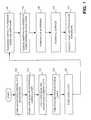
- FIG. 1illustrates an exemplary process for forming a fin in a FinFET device in an implementation consistent with the principles of the invention
- FIGS. 2-10illustrate exemplary cross-sectional views of a FinFET device fabricated according to the processing described in FIG. 1;
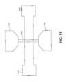
- FIG. 11illustrates an exemplary top view of a FinFET device fabricated according to the processing described in FIG. 1 .
- a narrow finmay be formed through the use of a sacrificial amorphous carbon layer.
- FIG. 1illustrates an exemplary process for fabricating a FinFET in an implementation consistent with the principles of the invention.
- FIGS. 2-11illustrate views of a FinFET fabricated according to the processing described in FIG. 1 .
- processingmay begin by depositing an amorphous carbon layer 230 on a silicon on insulator (SOI) structure (act 105 ).
- Amorphous carbon layer 230may be deposited in a conventional manner.
- amorphous carbon layer 230may have a thickness ranging from about 500 ⁇ to about 1500 ⁇ .
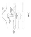
- the SOI structureincludes a silicon substrate 200 , a buried oxide layer 210 , and a silicon layer 220 on buried oxide layer 210 .
- Buried oxide layer 210 and silicon layer 220may be formed on substrate 200 in a conventional manner.
- buried oxide layer 210may include a silicon oxide and may have a thickness ranging from about 1500 ⁇ to about 3000 ⁇ .
- Silicon layer 220may be monocrystalline silicon having a thickness ranging from about 100 ⁇ to about 1000 ⁇ .
- substrate 200 and silicon layer 220may include other materials, such as germanium, or combinations of materials, such as silicon-germanium.
- Buried oxide layer 210may also include other dielectric materials.
- a hard mask 240may be deposited on amorphous carbon layer 230 , as illustrated in FIG. 2 (act 110 ).
- hard mask 240may include an oxide or nitride-based material. Other materials may alternatively be used.
- Hard mask 240may have a thickness ranging from about 200 ⁇ to about 500 ⁇ .
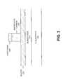
- Hard mask 240 and amorphous carbon layer 230may then be etched in a conventional manner, such as an anisotropic etch, with the etching terminating on silicon layer 220 , as illustrated in FIG. 3 (act 115 ).
- hard mask 240 and amorphous carbon layer 230may be etched to a width ranging from about 500 ⁇ to about 1000 ⁇ .
- a subsequent trim etchmay then be performed on amorphous carbon layer 230 to further reduce the width of amorphous carbon layer 230 , as illustrated in FIG. 4 (act 120 ).
- the resulting width of amorphous carbon layer 230 after etchingmay range from about 250 ⁇ to about 450 ⁇ .
- An oxide layer 510may then be deposited to cover amorphous carbon layer 230 and hard mask 240 , as illustrated in FIG. 5 (act 125 ).
- layer 510may consist of other films or materials that may be deposited or grown.
- Oxide layer 510 and hard mask 240may be planarized via a chemical-mechanical polish (CMP) or other conventional technique, with the planarizing terminating at the top surface of amorphous carbon layer 230 , as illustrated in FIG. 6 (act 130 ).
- Amorphous carbon layer 230may then be removed to create opening 700 via plasma oxidation of amorphous carbon layer 230 or another conventional technique, as illustrated in FIG. 7 (act 135 ).
- the width of opening 700corresponds to the reduced width of amorphous carbon layer 230 obtained in act 120 . It should be understood, however, that the particular width of opening 700 may vary based on the particular circuit requirements associated with the fin in the FinFET device that will be formed.
- silicon 810may be grown via, for example, selective epitaxy of silicon layer 220 , to fill opening 700 , as illustrated in FIG. 8 (act 140 ).
- a chemical-mechanical polish (CMP) or other similar techniquemay be performed, if necessary, to planarize the upper surface of the semiconductor device and to remove any silicon 810 that grows above the top surface of oxide layer 510 , as illustrated in FIG. 9 (act 145 ).
- CMPchemical-mechanical polish
- the portion of silicon layer 220 below the remaining portions of oxide layer 510are denoted as field silicon 910 .
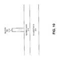
- a fin 1010may be formed by removing oxide layer 510 and field silicon 910 , as illustrated in FIG. 10 (act 150 ).
- the remaining oxide layer 510may be removed, for example, by etching or some other conventional technique.
- Field silicon 910may be removed via, for example, a highly anisotropic dry etch.
- the width of fin 1010may range from about 250 ⁇ to 450 ⁇ .
- the height of fin 1010may range from about 100 ⁇ to 1000 ⁇ .
- the particular width and height of fin 1010may vary based on the particular circuit requirements associated with the fin and FinFET device that will be formed.
- FIG. 11illustrates a top view of a semiconductor device consistent with the principles of the invention after the source/drain regions and gate electrodes are formed.
- the semiconductor devicemay include a double gate structure with fin 1010 , source drain regions 1110 and 1120 , and gate electrodes 1130 and 1140 .
- the source/drain regions 1110 and 1120may then be doped with n-type or p-type impurities based on the particular end device requirements.
- sidewall spacersmay optionally be formed prior to the source/drain ion implantation to control the location of the source/drain junctions based on the particular circuit requirements.
- Activation annealingmay then be performed to activate the source/drain regions 1110 and 1120 .
- the methodology of the present inventionmay be used to form any number of fins, based on the particular circuit requirements. For example, if more than one fin is to be formed, multiple amorphous carbon structures and subsequent openings may be formed (FIGS. 4 and 7 ). The processing for forming the fins may then proceed as described above with respect to acts 140 to 150 .
- a FinFET devicemay be formed with a narrow fin.
- a narrow finmay be formed through the use of a sacrificial amorphous carbon layer.
Landscapes
- Thin Film Transistor (AREA)
Abstract
Description
Claims (20)
Priority Applications (1)
| Application Number | Priority Date | Filing Date | Title |
|---|---|---|---|
| US10/310,926US6645797B1 (en) | 2002-12-06 | 2002-12-06 | Method for forming fins in a FinFET device using sacrificial carbon layer |
Applications Claiming Priority (1)
| Application Number | Priority Date | Filing Date | Title |
|---|---|---|---|
| US10/310,926US6645797B1 (en) | 2002-12-06 | 2002-12-06 | Method for forming fins in a FinFET device using sacrificial carbon layer |
Publications (1)
| Publication Number | Publication Date |
|---|---|
| US6645797B1true US6645797B1 (en) | 2003-11-11 |
Family
ID=29401205
Family Applications (1)
| Application Number | Title | Priority Date | Filing Date |
|---|---|---|---|
| US10/310,926Expired - LifetimeUS6645797B1 (en) | 2002-12-06 | 2002-12-06 | Method for forming fins in a FinFET device using sacrificial carbon layer |
Country Status (1)
| Country | Link |
|---|---|
| US (1) | US6645797B1 (en) |
Cited By (104)
| Publication number | Priority date | Publication date | Assignee | Title |
|---|---|---|---|---|
| US20040018738A1 (en)* | 2002-07-22 | 2004-01-29 | Wei Liu | Method for fabricating a notch gate structure of a field effect transistor |
| US20040036126A1 (en)* | 2002-08-23 | 2004-02-26 | Chau Robert S. | Tri-gate devices and methods of fabrication |
| US20040110097A1 (en)* | 2002-12-06 | 2004-06-10 | Ahmed Shibly S. | Double gate semiconductor device having a metal gate |
| US6756643B1 (en)* | 2003-06-12 | 2004-06-29 | Advanced Micro Devices, Inc. | Dual silicon layer for chemical mechanical polishing planarization |
| US6762448B1 (en)* | 2003-04-03 | 2004-07-13 | Advanced Micro Devices, Inc. | FinFET device with multiple fin structures |
| US20040197975A1 (en)* | 2003-01-23 | 2004-10-07 | Zoran Krivokapic | Narrow fin finfet |
| US6812119B1 (en)* | 2003-07-08 | 2004-11-02 | Advanced Micro Devices, Inc. | Narrow fins by oxidation in double-gate finfet |
| US20040222477A1 (en)* | 2003-05-05 | 2004-11-11 | International Business Machines Corporation | Multi-height finfets |
| US6864164B1 (en)* | 2002-12-17 | 2005-03-08 | Advanced Micro Devices, Inc. | Finfet gate formation using reverse trim of dummy gate |
| US20050104091A1 (en)* | 2003-11-04 | 2005-05-19 | Tabery Cyrus E. | Self aligned damascene gate |
| US20050148137A1 (en)* | 2003-12-30 | 2005-07-07 | Brask Justin K. | Nonplanar transistors with metal gate electrodes |
| US20050153486A1 (en)* | 2004-01-12 | 2005-07-14 | Advanced Micro Devices, Inc. | Method of fabricating a strained silicon channel FinFET |
| US20050153492A1 (en)* | 2004-01-12 | 2005-07-14 | Ahmed Shibly S. | Damascene tri-gate FinFET |
| US20050156202A1 (en)* | 2004-01-17 | 2005-07-21 | Hwa-Sung Rhee | At least penta-sided-channel type of FinFET transistor |
| WO2005071730A1 (en)* | 2004-01-16 | 2005-08-04 | Intel Corporation | Tri-gate transistors and mehtods to fabricate same |
| US20050214993A1 (en)* | 2004-02-03 | 2005-09-29 | Stmicroelectronics Sa | Process for producing a field-effect transistor and transistor thus obtained |
| US20050218438A1 (en)* | 2004-03-31 | 2005-10-06 | Nick Lindert | Bulk non-planar transistor having strained enhanced mobility and methods of fabrication |
| US20050255643A1 (en)* | 2004-05-14 | 2005-11-17 | Samsung Electronics Co., Ltd. | Method of forming fin field effect transistor using damascene process |
| US20050280102A1 (en)* | 2004-06-16 | 2005-12-22 | Chang-Woo Oh | Field effect transistor and method for manufacturing the same |
| US20050287772A1 (en)* | 2004-06-07 | 2005-12-29 | Infineon Technologies Ag | Process for producing a web of a semiconductor material |
| US20060001109A1 (en)* | 2004-06-30 | 2006-01-05 | Shaheen Mohamad A | High mobility tri-gate devices and methods of fabrication |
| US20060024945A1 (en)* | 2004-07-29 | 2006-02-02 | Hynix Semiconductor, Inc. | Method for fabricating semiconductor device using amorphous carbon layer as sacrificial hard mask |
| US20060029887A1 (en)* | 2004-08-06 | 2006-02-09 | Chang-Woo Oh | Semiconductor devices having a support structure for an active layer pattern and methods of forming the same |
| US20060063332A1 (en)* | 2004-09-23 | 2006-03-23 | Brian Doyle | U-gate transistors and methods of fabrication |
| US20060071275A1 (en)* | 2004-09-30 | 2006-04-06 | Brask Justin K | Nonplanar transistors with metal gate electrodes |
| US20060091433A1 (en)* | 2004-10-29 | 2006-05-04 | Kazumi Nishinohara | Semiconductor integrated circuit device and manufacturing method thereof |
| EP1555688A3 (en)* | 2004-01-17 | 2006-05-17 | Samsung Electronics Co., Ltd. | A multi-sided-channel finfet transistor and manufacturing method |
| US20060148154A1 (en)* | 2005-01-04 | 2006-07-06 | Dong-Suk Shin | Semiconductor devices having faceted channels and methods of fabricating such devices |
| US20060151834A1 (en)* | 2005-01-13 | 2006-07-13 | International Business Machines Corporation | High mobility plane finfet with equal drive strength |
| US20060157794A1 (en)* | 2005-01-18 | 2006-07-20 | Doyle Brian S | Non-planar MOS structure with a strained channel region |
| US20060166423A1 (en)* | 2005-01-21 | 2006-07-27 | Seiji Iseda | Removal spacer formation with carbon film |
| US7084018B1 (en)* | 2004-05-05 | 2006-08-01 | Advanced Micro Devices, Inc. | Sacrificial oxide for minimizing box undercut in damascene FinFET |
| US20060234138A1 (en)* | 2003-09-30 | 2006-10-19 | Rodger Fehlhaber | Hard mask arrangement |
| US20070001219A1 (en)* | 2005-06-30 | 2007-01-04 | Marko Radosavljevic | Block contact architectures for nanoscale channel transistors |
| US20070040223A1 (en)* | 2005-08-17 | 2007-02-22 | Intel Corporation | Lateral undercut of metal gate in SOI device |
| US20070045748A1 (en)* | 2005-08-25 | 2007-03-01 | International Business Machines Corporation | Semiconductor structures integrating damascene-body FinFET's and planar devices on a common substrate and methods for forming such semiconductor structures |
| US20070090416A1 (en)* | 2005-09-28 | 2007-04-26 | Doyle Brian S | CMOS devices with a single work function gate electrode and method of fabrication |
| EP1677350A3 (en)* | 2005-01-04 | 2007-05-30 | Samsung Electronics Co., Ltd. | Semiconductor device having surface regions with different crystal orientation and manufacturing method |
| US20070140637A1 (en)* | 2005-05-27 | 2007-06-21 | Staf Verhaegen | Method for high topography patterning |
| US7241653B2 (en) | 2003-06-27 | 2007-07-10 | Intel Corporation | Nonplanar device with stress incorporation layer and method of fabrication |
| CN1326217C (en)* | 2003-12-09 | 2007-07-11 | 国际商业机器公司 | Pull-back method of forming fins in FinFET |
| CN100352020C (en)* | 2004-03-01 | 2007-11-28 | 国际商业机器公司 | Method of manufacture of finfet devices with T-shaped fins and devices manufactured thereby |
| US7348284B2 (en) | 2004-08-10 | 2008-03-25 | Intel Corporation | Non-planar pMOS structure with a strained channel region and an integrated strained CMOS flow |
| US20080099839A1 (en)* | 2006-06-14 | 2008-05-01 | Willy Rachmady | Ultra-thin oxide bonding for S1 to S1 dual orientation bonding |
| US20080108222A1 (en)* | 2006-11-02 | 2008-05-08 | Hynix Semiconductor Inc. | Method for forming pattern in semiconductor device |
| US7396711B2 (en) | 2005-12-27 | 2008-07-08 | Intel Corporation | Method of fabricating a multi-cornered film |
| US20080203468A1 (en)* | 2007-02-28 | 2008-08-28 | Kangguo Cheng | FinFET with Reduced Gate to Fin Overlay Sensitivity |
| US20080206934A1 (en)* | 2007-02-23 | 2008-08-28 | Jones Robert E | Forming semiconductor fins using a sacrificial fin |
| US7432557B1 (en) | 2003-07-08 | 2008-10-07 | Advanced Micro Devices, Inc. | FinFET device with multiple channels |
| US7449373B2 (en) | 2006-03-31 | 2008-11-11 | Intel Corporation | Method of ion implanting for tri-gate devices |
| US7456476B2 (en) | 2003-06-27 | 2008-11-25 | Intel Corporation | Nonplanar semiconductor device with partially or fully wrapped around gate electrode and methods of fabrication |
| EP2009682A1 (en) | 2007-06-26 | 2008-12-31 | STMicroelectronics (Crolles 2) SAS | FinFET field-effect transistor isolated from the substrate |
| US7479421B2 (en) | 2005-09-28 | 2009-01-20 | Intel Corporation | Process for integrating planar and non-planar CMOS transistors on a bulk substrate and article made thereby |
| US7498225B1 (en) | 2003-12-04 | 2009-03-03 | Advanced Micro Devices, Inc. | Systems and methods for forming multiple fin structures using metal-induced-crystallization |
| US7518196B2 (en) | 2005-02-23 | 2009-04-14 | Intel Corporation | Field effect transistor with narrow bandgap source and drain regions and method of fabrication |
| US20090124097A1 (en)* | 2007-11-09 | 2009-05-14 | International Business Machines Corporation | Method of forming narrow fins in finfet devices with reduced spacing therebetween |
| US7547637B2 (en) | 2005-06-21 | 2009-06-16 | Intel Corporation | Methods for patterning a semiconductor film |
| US7550333B2 (en) | 2004-10-25 | 2009-06-23 | Intel Corporation | Nonplanar device with thinned lower body portion and method of fabrication |
| US7579280B2 (en) | 2004-06-01 | 2009-08-25 | Intel Corporation | Method of patterning a film |
| CN100578758C (en)* | 2005-02-14 | 2010-01-06 | 台湾积体电路制造股份有限公司 | Method for manufacturing multi-grid field effect transistor element |
| US7679134B1 (en) | 2002-11-26 | 2010-03-16 | Globalfoundries | FinFET device with multiple fin structures |
| US7859053B2 (en) | 2004-09-29 | 2010-12-28 | Intel Corporation | Independently accessed double-gate and tri-gate transistors in same process flow |
| US7858481B2 (en) | 2005-06-15 | 2010-12-28 | Intel Corporation | Method for fabricating transistor with thinned channel |
| US20110021010A1 (en)* | 2009-07-27 | 2011-01-27 | International Business Machines Corporation | Method for double pattern density |
| US7879675B2 (en) | 2005-03-14 | 2011-02-01 | Intel Corporation | Field effect transistor with metal source/drain regions |
| US7915167B2 (en) | 2004-09-29 | 2011-03-29 | Intel Corporation | Fabrication of channel wraparound gate structure for field-effect transistor |
| US7915160B1 (en)* | 2003-12-08 | 2011-03-29 | Globalfoundries Inc. | Methods for forming small contacts |
| US7989280B2 (en) | 2005-11-30 | 2011-08-02 | Intel Corporation | Dielectric interface for group III-V semiconductor device |
| US20110204443A1 (en)* | 2010-02-23 | 2011-08-25 | International Business Machines Corporation | Semiconductor-on-insulator (soi) structure and method of forming the soi structure using a bulk semiconductor starting wafer |
| US8216951B2 (en) | 2006-09-27 | 2012-07-10 | Taiwan Semiconductor Manufacturing Company, Ltd. | Quantum tunneling devices and circuits with lattice-mismatched semiconductor structures |
| US8237151B2 (en) | 2009-01-09 | 2012-08-07 | Taiwan Semiconductor Manufacturing Company, Ltd. | Diode-based devices and methods for making the same |
| US8253211B2 (en) | 2008-09-24 | 2012-08-28 | Taiwan Semiconductor Manufacturing Company, Ltd. | Semiconductor sensor structures with reduced dislocation defect densities |
| US8274097B2 (en) | 2008-07-01 | 2012-09-25 | Taiwan Semiconductor Manufacturing Company, Ltd. | Reduction of edge effects from aspect ratio trapping |
| US8304805B2 (en) | 2009-01-09 | 2012-11-06 | Taiwan Semiconductor Manufacturing Company, Ltd. | Semiconductor diodes fabricated by aspect ratio trapping with coalesced films |
| US8324660B2 (en) | 2005-05-17 | 2012-12-04 | Taiwan Semiconductor Manufacturing Company, Ltd. | Lattice-mismatched semiconductor structures with reduced dislocation defect densities and related methods for device fabrication |
| US8329541B2 (en) | 2007-06-15 | 2012-12-11 | Taiwan Semiconductor Manufacturing Company, Ltd. | InP-based transistor fabrication |
| US8344242B2 (en) | 2007-09-07 | 2013-01-01 | Taiwan Semiconductor Manufacturing Company, Ltd. | Multi-junction solar cells |
| US8362566B2 (en) | 2008-06-23 | 2013-01-29 | Intel Corporation | Stress in trigate devices using complimentary gate fill materials |
| US8384196B2 (en) | 2008-09-19 | 2013-02-26 | Taiwan Semiconductor Manufacturing Company, Ltd. | Formation of devices by epitaxial layer overgrowth |
| US8502263B2 (en) | 2006-10-19 | 2013-08-06 | Taiwan Semiconductor Manufacturing Company, Ltd. | Light-emitter-based devices with lattice-mismatched semiconductor structures |
| TWI409857B (en)* | 2006-01-23 | 2013-09-21 | Lam Res Corp | Fin structure formation |
| CN103413758A (en)* | 2013-07-17 | 2013-11-27 | 华为技术有限公司 | Manufacturing method for semiconductor fin ray and manufacturing method for FinFET device |
| US8617945B2 (en) | 2006-08-02 | 2013-12-31 | Intel Corporation | Stacking fault and twin blocking barrier for integrating III-V on Si |
| US8624103B2 (en) | 2007-04-09 | 2014-01-07 | Taiwan Semiconductor Manufacturing Company, Ltd. | Nitride-based multi-junction solar cell modules and methods for making the same |
| US8629446B2 (en) | 2009-04-02 | 2014-01-14 | Taiwan Semiconductor Manufacturing Company, Ltd. | Devices formed from a non-polar plane of a crystalline material and method of making the same |
| US8722494B1 (en) | 2012-11-01 | 2014-05-13 | International Business Machines Corporation | Dual gate finFET devices |
| US8822248B2 (en) | 2008-06-03 | 2014-09-02 | Taiwan Semiconductor Manufacturing Company, Ltd. | Epitaxial growth of crystalline material |
| US8847279B2 (en) | 2006-09-07 | 2014-09-30 | Taiwan Semiconductor Manufacturing Company, Ltd. | Defect reduction using aspect ratio trapping |
| US8878243B2 (en) | 2006-03-24 | 2014-11-04 | Taiwan Semiconductor Manufacturing Company, Ltd. | Lattice-mismatched semiconductor structures and related methods for device fabrication |
| CN104217961A (en)* | 2013-05-31 | 2014-12-17 | 意法半导体公司 | Method of making a semiconductor device using sacrificial fins |
| US8975168B2 (en) | 2013-05-28 | 2015-03-10 | Stmicroelectronics, Inc. | Method for the formation of fin structures for FinFET devices |
| US8981427B2 (en) | 2008-07-15 | 2015-03-17 | Taiwan Semiconductor Manufacturing Company, Ltd. | Polishing of small composite semiconductor materials |
| US9099570B2 (en) | 2013-12-05 | 2015-08-04 | Stmicroelectronics, Inc. | Method for the formation of dielectric isolated fin structures for use, for example, in FinFET devices |
| US9136384B2 (en) | 2013-12-05 | 2015-09-15 | Stmicroelectronics, Inc. | Method for the formation of a FinFET device having partially dielectric isolated Fin structure |
| US20150270341A1 (en)* | 2012-10-18 | 2015-09-24 | Institute of Microelectronics, Chinese Academy of Sciences | Method for manufacturing fin structure of finfet |
| US9263586B2 (en) | 2014-06-06 | 2016-02-16 | Taiwan Semiconductor Manufacturing Company, Ltd. | Quantum well fin-like field effect transistor (QWFinFET) having a two-section combo QW structure |
| US9401303B2 (en) | 2014-08-01 | 2016-07-26 | Globalfoundries Inc. | Handler wafer removal by use of sacrificial inert layer |
| US9406746B2 (en) | 2014-02-19 | 2016-08-02 | International Business Machines Corporation | Work function metal fill for replacement gate fin field effect transistor process |
| US9508890B2 (en) | 2007-04-09 | 2016-11-29 | Taiwan Semiconductor Manufacturing Company, Ltd. | Photovoltaics on silicon |
| US9601382B2 (en) | 2013-12-05 | 2017-03-21 | Stmicroelectronics (Crolles 2) Sas | Method for the formation of a FinFET device with epitaxially grown source-drain regions having a reduced leakage path |
| US9853160B2 (en) | 2015-05-26 | 2017-12-26 | Samsung Electronics Co., Ltd. | Semiconductor devices and methods of fabricating the same |
| US9859381B2 (en) | 2005-05-17 | 2018-01-02 | Taiwan Semiconductor Manufacturing Company, Ltd. | Lattice-mismatched semiconductor structures with reduced dislocation defect densities and related methods for device fabrication |
| US9984872B2 (en) | 2008-09-19 | 2018-05-29 | Taiwan Semiconductor Manufacturing Company, Ltd. | Fabrication and structures of crystalline material |
| RU2698574C1 (en)* | 2018-11-28 | 2019-08-28 | Акционерное общество "Научно-исследовательский институт молекулярной электроники" | Method of making a semiconductor structure protruding from a monolithic silicon body |
Citations (4)
| Publication number | Priority date | Publication date | Assignee | Title |
|---|---|---|---|---|
| US6316296B1 (en)* | 1999-05-28 | 2001-11-13 | Agency Of Industrial Science & Technology, Ministry Of International Trade & Industry | Field-effect transistor and method of manufacturing same |
| US6413802B1 (en)* | 2000-10-23 | 2002-07-02 | The Regents Of The University Of California | Finfet transistor structures having a double gate channel extending vertically from a substrate and methods of manufacture |
| US6432829B2 (en)* | 1999-12-09 | 2002-08-13 | International Business Machines Corporation | Process for making planarized silicon fin device |
| US6525403B2 (en)* | 2000-09-28 | 2003-02-25 | Kabushiki Kaisha Toshiba | Semiconductor device having MIS field effect transistors or three-dimensional structure |
- 2002
- 2002-12-06USUS10/310,926patent/US6645797B1/ennot_activeExpired - Lifetime
Patent Citations (4)
| Publication number | Priority date | Publication date | Assignee | Title |
|---|---|---|---|---|
| US6316296B1 (en)* | 1999-05-28 | 2001-11-13 | Agency Of Industrial Science & Technology, Ministry Of International Trade & Industry | Field-effect transistor and method of manufacturing same |
| US6432829B2 (en)* | 1999-12-09 | 2002-08-13 | International Business Machines Corporation | Process for making planarized silicon fin device |
| US6525403B2 (en)* | 2000-09-28 | 2003-02-25 | Kabushiki Kaisha Toshiba | Semiconductor device having MIS field effect transistors or three-dimensional structure |
| US6413802B1 (en)* | 2000-10-23 | 2002-07-02 | The Regents Of The University Of California | Finfet transistor structures having a double gate channel extending vertically from a substrate and methods of manufacture |
Non-Patent Citations (5)
| Title |
|---|
| Digh Hisamoto et al., "FinFET-A Self-Aligned Double-Gate MOSFET Scalable to 20 nm," IEEE Transactions on Electron Devices, vol. 47, No. 12, Dec. 2000, pp. 2320-2325. |
| Xuejue Huang et al., "Sub 50-nm FinFET: PMOS," 1999 IEEE, IEDM, pp. 67-70. |
| Xuejue Huang et al., "Sub-50 nm P-Channel FinFET," IEEE Transactions on Electron Devices, vol. 48, No. 5, May 2001, pp. 880-886. |
| Yang-Kyu Choi et al., "Nanoscale CMOS Spacer FinFET for the Terabit Era," IEEE Electron Device Letters, vol. 23, No. 1, Jan. 2002, pp. 25-27. |
| Yang-Kyu Choi et al., "Sub-20nm CMOS FinFET Technologies," 2001 IEEE IEDM, pp. 421-424. |
Cited By (271)
| Publication number | Priority date | Publication date | Assignee | Title |
|---|---|---|---|---|
| US20040018738A1 (en)* | 2002-07-22 | 2004-01-29 | Wei Liu | Method for fabricating a notch gate structure of a field effect transistor |
| US7368791B2 (en) | 2002-08-23 | 2008-05-06 | Intel Corporation | Multi-gate carbon nano-tube transistors |
| US7358121B2 (en) | 2002-08-23 | 2008-04-15 | Intel Corporation | Tri-gate devices and methods of fabrication |
| US7514346B2 (en) | 2002-08-23 | 2009-04-07 | Intel Corporation | Tri-gate devices and methods of fabrication |
| US7504678B2 (en) | 2002-08-23 | 2009-03-17 | Intel Corporation | Tri-gate devices and methods of fabrication |
| US20060228840A1 (en)* | 2002-08-23 | 2006-10-12 | Chau Robert S | Tri-gate devices and methods of fabrication |
| US7427794B2 (en) | 2002-08-23 | 2008-09-23 | Intel Corporation | Tri-gate devices and methods of fabrication |
| US7560756B2 (en) | 2002-08-23 | 2009-07-14 | Intel Corporation | Tri-gate devices and methods of fabrication |
| US20040036126A1 (en)* | 2002-08-23 | 2004-02-26 | Chau Robert S. | Tri-gate devices and methods of fabrication |
| US7679134B1 (en) | 2002-11-26 | 2010-03-16 | Globalfoundries | FinFET device with multiple fin structures |
| US20040110097A1 (en)* | 2002-12-06 | 2004-06-10 | Ahmed Shibly S. | Double gate semiconductor device having a metal gate |
| US7256455B2 (en) | 2002-12-06 | 2007-08-14 | Advanced Micro Devices, Inc. | Double gate semiconductor device having a metal gate |
| US6864164B1 (en)* | 2002-12-17 | 2005-03-08 | Advanced Micro Devices, Inc. | Finfet gate formation using reverse trim of dummy gate |
| US20040197975A1 (en)* | 2003-01-23 | 2004-10-07 | Zoran Krivokapic | Narrow fin finfet |
| US6921963B2 (en) | 2003-01-23 | 2005-07-26 | Advanced Micro Devices, Inc | Narrow fin FinFET |
| US6852576B2 (en) | 2003-04-03 | 2005-02-08 | Advanced Micro Devices, Inc. | Method for forming structures in finfet devices |
| US20040198031A1 (en)* | 2003-04-03 | 2004-10-07 | Ming-Ren Lin | Method for forming structures in finfet devices |
| US6762448B1 (en)* | 2003-04-03 | 2004-07-13 | Advanced Micro Devices, Inc. | FinFET device with multiple fin structures |
| US6909147B2 (en)* | 2003-05-05 | 2005-06-21 | International Business Machines Corporation | Multi-height FinFETS |
| WO2004100290A3 (en)* | 2003-05-05 | 2005-02-24 | Ibm | Multi-height finfets |
| US20040222477A1 (en)* | 2003-05-05 | 2004-11-11 | International Business Machines Corporation | Multi-height finfets |
| US6812076B1 (en) | 2003-06-12 | 2004-11-02 | Advanced Micro Devices, Inc. | Dual silicon layer for chemical mechanical polishing planarization |
| US20050056845A1 (en)* | 2003-06-12 | 2005-03-17 | Krishnashree Achuthan | Dual silicon layer for chemical mechanical polishing planarization |
| US6756643B1 (en)* | 2003-06-12 | 2004-06-29 | Advanced Micro Devices, Inc. | Dual silicon layer for chemical mechanical polishing planarization |
| US6982464B2 (en) | 2003-06-12 | 2006-01-03 | Advanced Micro Devices, Inc. | Dual silicon layer for chemical mechanical polishing planarization |
| US7456476B2 (en) | 2003-06-27 | 2008-11-25 | Intel Corporation | Nonplanar semiconductor device with partially or fully wrapped around gate electrode and methods of fabrication |
| US8405164B2 (en) | 2003-06-27 | 2013-03-26 | Intel Corporation | Tri-gate transistor device with stress incorporation layer and method of fabrication |
| US8273626B2 (en) | 2003-06-27 | 2012-09-25 | Intel Corporationn | Nonplanar semiconductor device with partially or fully wrapped around gate electrode and methods of fabrication |
| US7241653B2 (en) | 2003-06-27 | 2007-07-10 | Intel Corporation | Nonplanar device with stress incorporation layer and method of fabrication |
| US7714397B2 (en) | 2003-06-27 | 2010-05-11 | Intel Corporation | Tri-gate transistor device with stress incorporation layer and method of fabrication |
| US7820513B2 (en) | 2003-06-27 | 2010-10-26 | Intel Corporation | Nonplanar semiconductor device with partially or fully wrapped around gate electrode and methods of fabrication |
| US7432557B1 (en) | 2003-07-08 | 2008-10-07 | Advanced Micro Devices, Inc. | FinFET device with multiple channels |
| US6812119B1 (en)* | 2003-07-08 | 2004-11-02 | Advanced Micro Devices, Inc. | Narrow fins by oxidation in double-gate finfet |
| US20060234138A1 (en)* | 2003-09-30 | 2006-10-19 | Rodger Fehlhaber | Hard mask arrangement |
| US7029958B2 (en) | 2003-11-04 | 2006-04-18 | Advanced Micro Devices, Inc. | Self aligned damascene gate |
| US20050104091A1 (en)* | 2003-11-04 | 2005-05-19 | Tabery Cyrus E. | Self aligned damascene gate |
| US7498225B1 (en) | 2003-12-04 | 2009-03-03 | Advanced Micro Devices, Inc. | Systems and methods for forming multiple fin structures using metal-induced-crystallization |
| US7915160B1 (en)* | 2003-12-08 | 2011-03-29 | Globalfoundries Inc. | Methods for forming small contacts |
| CN1326217C (en)* | 2003-12-09 | 2007-07-11 | 国际商业机器公司 | Pull-back method of forming fins in FinFET |
| US7329913B2 (en) | 2003-12-30 | 2008-02-12 | Intel Corporation | Nonplanar transistors with metal gate electrodes |
| US20050148137A1 (en)* | 2003-12-30 | 2005-07-07 | Brask Justin K. | Nonplanar transistors with metal gate electrodes |
| US7105390B2 (en) | 2003-12-30 | 2006-09-12 | Intel Corporation | Nonplanar transistors with metal gate electrodes |
| DE112004002641B4 (en)* | 2004-01-12 | 2009-01-02 | Advanced Micro Devices, Inc., Sunnyvale | Method of making a deformed FinFET channel |
| US7041542B2 (en) | 2004-01-12 | 2006-05-09 | Advanced Micro Devices, Inc. | Damascene tri-gate FinFET |
| WO2005071728A1 (en)* | 2004-01-12 | 2005-08-04 | Advanced Micro Devices, Inc. | Method of fabricating a strained finfet channel |
| US7138302B2 (en) | 2004-01-12 | 2006-11-21 | Advanced Micro Devices, Inc. | Method of fabricating an integrated circuit channel region |
| US20050153492A1 (en)* | 2004-01-12 | 2005-07-14 | Ahmed Shibly S. | Damascene tri-gate FinFET |
| US20050153486A1 (en)* | 2004-01-12 | 2005-07-14 | Advanced Micro Devices, Inc. | Method of fabricating a strained silicon channel FinFET |
| WO2005071730A1 (en)* | 2004-01-16 | 2005-08-04 | Intel Corporation | Tri-gate transistors and mehtods to fabricate same |
| US7268058B2 (en) | 2004-01-16 | 2007-09-11 | Intel Corporation | Tri-gate transistors and methods to fabricate same |
| JP2007521667A (en)* | 2004-01-16 | 2007-08-02 | インテル コーポレイション | Tri-gate transistor and manufacturing method thereof |
| EP1555688A3 (en)* | 2004-01-17 | 2006-05-17 | Samsung Electronics Co., Ltd. | A multi-sided-channel finfet transistor and manufacturing method |
| US20080242010A1 (en)* | 2004-01-17 | 2008-10-02 | Hwa-Sung Rhee | At least penta-sided-channel type of finfet transistor |
| US7385247B2 (en) | 2004-01-17 | 2008-06-10 | Samsung Electronics Co., Ltd. | At least penta-sided-channel type of FinFET transistor |
| US7723193B2 (en) | 2004-01-17 | 2010-05-25 | Samsung Electronics Co., Ltd. | Method of forming an at least penta-sided-channel type of FinFET transistor |
| US20050156202A1 (en)* | 2004-01-17 | 2005-07-21 | Hwa-Sung Rhee | At least penta-sided-channel type of FinFET transistor |
| US7229867B2 (en)* | 2004-02-03 | 2007-06-12 | Stmicroelectronics Sa | Process for producing a field-effect transistor and transistor thus obtained |
| US20050214993A1 (en)* | 2004-02-03 | 2005-09-29 | Stmicroelectronics Sa | Process for producing a field-effect transistor and transistor thus obtained |
| CN100352020C (en)* | 2004-03-01 | 2007-11-28 | 国际商业机器公司 | Method of manufacture of finfet devices with T-shaped fins and devices manufactured thereby |
| CN101189730B (en)* | 2004-03-31 | 2011-04-20 | 英特尔公司 | Non-planar bulk transistor with strained channel for enhanced mobility and method of fabrication |
| US7326634B2 (en) | 2004-03-31 | 2008-02-05 | Intel Corporation | Bulk non-planar transistor having strained enhanced mobility and methods of fabrication |
| US20050218438A1 (en)* | 2004-03-31 | 2005-10-06 | Nick Lindert | Bulk non-planar transistor having strained enhanced mobility and methods of fabrication |
| US20050224800A1 (en)* | 2004-03-31 | 2005-10-13 | Nick Lindert | Bulk non-planar transistor having strained enhanced mobility and methods of fabrication |
| US7154118B2 (en) | 2004-03-31 | 2006-12-26 | Intel Corporation | Bulk non-planar transistor having strained enhanced mobility and methods of fabrication |
| US7781771B2 (en) | 2004-03-31 | 2010-08-24 | Intel Corporation | Bulk non-planar transistor having strained enhanced mobility and methods of fabrication |
| WO2005098963A1 (en)* | 2004-03-31 | 2005-10-20 | Intel Corporation | A bulk non-planar transistor having a strained channel with enhanced mobility and methods of fabrication |
| US7084018B1 (en)* | 2004-05-05 | 2006-08-01 | Advanced Micro Devices, Inc. | Sacrificial oxide for minimizing box undercut in damascene FinFET |
| US7528022B2 (en) | 2004-05-14 | 2009-05-05 | Samsung Electronics Co., Ltd. | Method of forming fin field effect transistor using damascene process |
| US20050255643A1 (en)* | 2004-05-14 | 2005-11-17 | Samsung Electronics Co., Ltd. | Method of forming fin field effect transistor using damascene process |
| US7579280B2 (en) | 2004-06-01 | 2009-08-25 | Intel Corporation | Method of patterning a film |
| US20050287772A1 (en)* | 2004-06-07 | 2005-12-29 | Infineon Technologies Ag | Process for producing a web of a semiconductor material |
| US20050280102A1 (en)* | 2004-06-16 | 2005-12-22 | Chang-Woo Oh | Field effect transistor and method for manufacturing the same |
| US7042009B2 (en) | 2004-06-30 | 2006-05-09 | Intel Corporation | High mobility tri-gate devices and methods of fabrication |
| US20060001109A1 (en)* | 2004-06-30 | 2006-01-05 | Shaheen Mohamad A | High mobility tri-gate devices and methods of fabrication |
| US8084818B2 (en) | 2004-06-30 | 2011-12-27 | Intel Corporation | High mobility tri-gate devices and methods of fabrication |
| US7446049B2 (en)* | 2004-07-29 | 2008-11-04 | Hynix Semiconductor Inc. | Method for fabricating semiconductor device using amorphous carbon layer as sacrificial hard mask |
| US20060024945A1 (en)* | 2004-07-29 | 2006-02-02 | Hynix Semiconductor, Inc. | Method for fabricating semiconductor device using amorphous carbon layer as sacrificial hard mask |
| US7989854B2 (en) | 2004-08-06 | 2011-08-02 | Samsung Electronics Co., Ltd. | Semiconductor devices having a support structure for an active layer pattern |
| US20060029887A1 (en)* | 2004-08-06 | 2006-02-09 | Chang-Woo Oh | Semiconductor devices having a support structure for an active layer pattern and methods of forming the same |
| US8426901B2 (en) | 2004-08-06 | 2013-04-23 | Samsung Electronics Co., Ltd. | Semiconductor devices having a support structure for an active layer pattern |
| US8815702B2 (en) | 2004-08-06 | 2014-08-26 | Samsung Electronics Co., Ltd. | Methods of manufacturing semiconductor devices having a support structure for an active layer pattern |
| US7960794B2 (en) | 2004-08-10 | 2011-06-14 | Intel Corporation | Non-planar pMOS structure with a strained channel region and an integrated strained CMOS flow |
| US7348284B2 (en) | 2004-08-10 | 2008-03-25 | Intel Corporation | Non-planar pMOS structure with a strained channel region and an integrated strained CMOS flow |
| US20060063332A1 (en)* | 2004-09-23 | 2006-03-23 | Brian Doyle | U-gate transistors and methods of fabrication |
| US7859053B2 (en) | 2004-09-29 | 2010-12-28 | Intel Corporation | Independently accessed double-gate and tri-gate transistors in same process flow |
| US8268709B2 (en) | 2004-09-29 | 2012-09-18 | Intel Corporation | Independently accessed double-gate and tri-gate transistors in same process flow |
| US7915167B2 (en) | 2004-09-29 | 2011-03-29 | Intel Corporation | Fabrication of channel wraparound gate structure for field-effect transistor |
| US8399922B2 (en) | 2004-09-29 | 2013-03-19 | Intel Corporation | Independently accessed double-gate and tri-gate transistors |
| US7326656B2 (en) | 2004-09-30 | 2008-02-05 | Intel Corporation | Method of forming a metal oxide dielectric |
| US20060071275A1 (en)* | 2004-09-30 | 2006-04-06 | Brask Justin K | Nonplanar transistors with metal gate electrodes |
| US7531437B2 (en) | 2004-09-30 | 2009-05-12 | Intel Corporation | Method of forming metal gate electrodes using sacrificial gate electrode material and sacrificial gate dielectric material |
| US20060138553A1 (en)* | 2004-09-30 | 2006-06-29 | Brask Justin K | Nonplanar transistors with metal gate electrodes |
| US7528025B2 (en) | 2004-09-30 | 2009-05-05 | Intel Corporation | Nonplanar transistors with metal gate electrodes |
| US7361958B2 (en) | 2004-09-30 | 2008-04-22 | Intel Corporation | Nonplanar transistors with metal gate electrodes |
| US20060138552A1 (en)* | 2004-09-30 | 2006-06-29 | Brask Justin K | Nonplanar transistors with metal gate electrodes |
| US8749026B2 (en) | 2004-10-25 | 2014-06-10 | Intel Corporation | Nonplanar device with thinned lower body portion and method of fabrication |
| US8067818B2 (en) | 2004-10-25 | 2011-11-29 | Intel Corporation | Nonplanar device with thinned lower body portion and method of fabrication |
| US10236356B2 (en) | 2004-10-25 | 2019-03-19 | Intel Corporation | Nonplanar device with thinned lower body portion and method of fabrication |
| US7550333B2 (en) | 2004-10-25 | 2009-06-23 | Intel Corporation | Nonplanar device with thinned lower body portion and method of fabrication |
| US8502351B2 (en) | 2004-10-25 | 2013-08-06 | Intel Corporation | Nonplanar device with thinned lower body portion and method of fabrication |
| US9190518B2 (en) | 2004-10-25 | 2015-11-17 | Intel Corporation | Nonplanar device with thinned lower body portion and method of fabrication |
| US9741809B2 (en) | 2004-10-25 | 2017-08-22 | Intel Corporation | Nonplanar device with thinned lower body portion and method of fabrication |
| US20060091433A1 (en)* | 2004-10-29 | 2006-05-04 | Kazumi Nishinohara | Semiconductor integrated circuit device and manufacturing method thereof |
| US7671420B2 (en) | 2005-01-04 | 2010-03-02 | Samsung Electronics Co., Ltd. | Semiconductor devices having faceted channels and methods of fabricating such devices |
| EP1677350A3 (en)* | 2005-01-04 | 2007-05-30 | Samsung Electronics Co., Ltd. | Semiconductor device having surface regions with different crystal orientation and manufacturing method |
| US20060148154A1 (en)* | 2005-01-04 | 2006-07-06 | Dong-Suk Shin | Semiconductor devices having faceted channels and methods of fabricating such devices |
| US7256078B2 (en) | 2005-01-13 | 2007-08-14 | International Business Machines Corporation | High mobility plane FinFETs with equal drive strength |
| US7196380B2 (en) | 2005-01-13 | 2007-03-27 | International Business Machines Corporation | High mobility plane FinFET with equal drive strength |
| US20070111410A1 (en)* | 2005-01-13 | 2007-05-17 | Anderson Brent A | High mobility plane finfets with equal drive strength |
| US20060151834A1 (en)* | 2005-01-13 | 2006-07-13 | International Business Machines Corporation | High mobility plane finfet with equal drive strength |
| US7193279B2 (en) | 2005-01-18 | 2007-03-20 | Intel Corporation | Non-planar MOS structure with a strained channel region |
| US7531393B2 (en) | 2005-01-18 | 2009-05-12 | Intel Corporation | Non-planar MOS structure with a strained channel region |
| US20060157687A1 (en)* | 2005-01-18 | 2006-07-20 | Doyle Brian S | Non-planar MOS structure with a strained channel region |
| US20060157794A1 (en)* | 2005-01-18 | 2006-07-20 | Doyle Brian S | Non-planar MOS structure with a strained channel region |
| US20060166423A1 (en)* | 2005-01-21 | 2006-07-27 | Seiji Iseda | Removal spacer formation with carbon film |
| CN100578758C (en)* | 2005-02-14 | 2010-01-06 | 台湾积体电路制造股份有限公司 | Method for manufacturing multi-grid field effect transistor element |
| US8816394B2 (en) | 2005-02-23 | 2014-08-26 | Intel Corporation | Field effect transistor with narrow bandgap source and drain regions and method of fabrication |
| US8183646B2 (en) | 2005-02-23 | 2012-05-22 | Intel Corporation | Field effect transistor with narrow bandgap source and drain regions and method of fabrication |
| US8664694B2 (en) | 2005-02-23 | 2014-03-04 | Intel Corporation | Field effect transistor with narrow bandgap source and drain regions and method of fabrication |
| US9368583B2 (en) | 2005-02-23 | 2016-06-14 | Intel Corporation | Field effect transistor with narrow bandgap source and drain regions and method of fabrication |
| US9048314B2 (en) | 2005-02-23 | 2015-06-02 | Intel Corporation | Field effect transistor with narrow bandgap source and drain regions and method of fabrication |
| US7893506B2 (en) | 2005-02-23 | 2011-02-22 | Intel Corporation | Field effect transistor with narrow bandgap source and drain regions and method of fabrication |
| US8368135B2 (en) | 2005-02-23 | 2013-02-05 | Intel Corporation | Field effect transistor with narrow bandgap source and drain regions and method of fabrication |
| US7825481B2 (en) | 2005-02-23 | 2010-11-02 | Intel Corporation | Field effect transistor with narrow bandgap source and drain regions and method of fabrication |
| US7518196B2 (en) | 2005-02-23 | 2009-04-14 | Intel Corporation | Field effect transistor with narrow bandgap source and drain regions and method of fabrication |
| US7879675B2 (en) | 2005-03-14 | 2011-02-01 | Intel Corporation | Field effect transistor with metal source/drain regions |
| US11251272B2 (en) | 2005-05-17 | 2022-02-15 | Taiwan Semiconductor Manufacturing Company, Ltd. | Lattice-mismatched semiconductor structures with reduced dislocation defect densities and related methods for device fabrication |
| US9859381B2 (en) | 2005-05-17 | 2018-01-02 | Taiwan Semiconductor Manufacturing Company, Ltd. | Lattice-mismatched semiconductor structures with reduced dislocation defect densities and related methods for device fabrication |
| US10522629B2 (en) | 2005-05-17 | 2019-12-31 | Taiwan Semiconductor Manufacturing Company, Ltd. | Lattice-mismatched semiconductor structures with reduced dislocation defect densities and related methods for device fabrication |
| US8629477B2 (en) | 2005-05-17 | 2014-01-14 | Taiwan Semiconductor Manufacturing Company, Ltd. | Lattice-mismatched semiconductor structures with reduced dislocation defect densities and related methods for device fabrication |
| US8796734B2 (en) | 2005-05-17 | 2014-08-05 | Taiwan Semiconductor Manufacturing Company, Ltd. | Lattice-mismatched semiconductor structures with reduced dislocation defect densities and related methods for device fabrication |
| US8324660B2 (en) | 2005-05-17 | 2012-12-04 | Taiwan Semiconductor Manufacturing Company, Ltd. | Lattice-mismatched semiconductor structures with reduced dislocation defect densities and related methods for device fabrication |
| US8987028B2 (en) | 2005-05-17 | 2015-03-24 | Taiwan Semiconductor Manufacturing Company, Ltd. | Lattice-mismatched semiconductor structures with reduced dislocation defect densities and related methods for device fabrication |
| US9431243B2 (en) | 2005-05-17 | 2016-08-30 | Taiwan Semiconductor Manufacturing Company, Ltd. | Lattice-mismatched semiconductor structures with reduced dislocation defect densities and related methods for device fabrication |
| US9219112B2 (en) | 2005-05-17 | 2015-12-22 | Taiwan Semiconductor Manufacturing Company, Ltd. | Lattice-mismatched semiconductor structures with reduced dislocation defect densities and related methods for device fabrication |
| US8519436B2 (en) | 2005-05-17 | 2013-08-27 | Taiwan Semiconductor Manufacturing Company, Ltd. | Lattice-mismatched semiconductor structures with reduced dislocation defect densities and related methods for device fabrication |
| US8021989B2 (en)* | 2005-05-27 | 2011-09-20 | Imec | Method for high topography patterning |
| US20070140637A1 (en)* | 2005-05-27 | 2007-06-21 | Staf Verhaegen | Method for high topography patterning |
| US7858481B2 (en) | 2005-06-15 | 2010-12-28 | Intel Corporation | Method for fabricating transistor with thinned channel |
| US9806195B2 (en) | 2005-06-15 | 2017-10-31 | Intel Corporation | Method for fabricating transistor with thinned channel |
| US9337307B2 (en) | 2005-06-15 | 2016-05-10 | Intel Corporation | Method for fabricating transistor with thinned channel |
| US11978799B2 (en) | 2005-06-15 | 2024-05-07 | Tahoe Research, Ltd. | Method for fabricating transistor with thinned channel |
| US8933458B2 (en) | 2005-06-21 | 2015-01-13 | Intel Corporation | Semiconductor device structures and methods of forming semiconductor structures |
| US7547637B2 (en) | 2005-06-21 | 2009-06-16 | Intel Corporation | Methods for patterning a semiconductor film |
| US8071983B2 (en) | 2005-06-21 | 2011-12-06 | Intel Corporation | Semiconductor device structures and methods of forming semiconductor structures |
| US8581258B2 (en) | 2005-06-21 | 2013-11-12 | Intel Corporation | Semiconductor device structures and methods of forming semiconductor structures |
| US9385180B2 (en) | 2005-06-21 | 2016-07-05 | Intel Corporation | Semiconductor device structures and methods of forming semiconductor structures |
| US9761724B2 (en) | 2005-06-21 | 2017-09-12 | Intel Corporation | Semiconductor device structures and methods of forming semiconductor structures |
| US7279375B2 (en) | 2005-06-30 | 2007-10-09 | Intel Corporation | Block contact architectures for nanoscale channel transistors |
| US7898041B2 (en) | 2005-06-30 | 2011-03-01 | Intel Corporation | Block contact architectures for nanoscale channel transistors |
| US20070001219A1 (en)* | 2005-06-30 | 2007-01-04 | Marko Radosavljevic | Block contact architectures for nanoscale channel transistors |
| US7402875B2 (en) | 2005-08-17 | 2008-07-22 | Intel Corporation | Lateral undercut of metal gate in SOI device |
| US20070040223A1 (en)* | 2005-08-17 | 2007-02-22 | Intel Corporation | Lateral undercut of metal gate in SOI device |
| US7736956B2 (en) | 2005-08-17 | 2010-06-15 | Intel Corporation | Lateral undercut of metal gate in SOI device |
| US20080048265A1 (en)* | 2005-08-25 | 2008-02-28 | International Business Machines Corporation | Semiconductor structures integrating damascene-body finfet's and planar devices on a common substrate and methods for forming such semiconductor structures |
| US20080050866A1 (en)* | 2005-08-25 | 2008-02-28 | International Business Machines Corporation | Semiconductor structures integrating damascene-body finfet's and planar devices on a common substrate and methods for forming such semiconductor structures |
| US20070045748A1 (en)* | 2005-08-25 | 2007-03-01 | International Business Machines Corporation | Semiconductor structures integrating damascene-body FinFET's and planar devices on a common substrate and methods for forming such semiconductor structures |
| US7352034B2 (en)* | 2005-08-25 | 2008-04-01 | International Business Machines Corporation | Semiconductor structures integrating damascene-body FinFET's and planar devices on a common substrate and methods for forming such semiconductor structures |
| US7879660B2 (en) | 2005-08-25 | 2011-02-01 | International Business Machines Corporation | Semiconductor structures integrating damascene-body FinFET's and planar devices on a common substrate and methods for forming such semiconductor structures |
| US7692250B2 (en) | 2005-08-25 | 2010-04-06 | International Business Machines Corporation | Semiconductor structures integrating damascene-body FinFET's and planar devices on a common substrate and methods for forming such semiconductor structures |
| US8294180B2 (en) | 2005-09-28 | 2012-10-23 | Intel Corporation | CMOS devices with a single work function gate electrode and method of fabrication |
| US7902014B2 (en) | 2005-09-28 | 2011-03-08 | Intel Corporation | CMOS devices with a single work function gate electrode and method of fabrication |
| US20070090416A1 (en)* | 2005-09-28 | 2007-04-26 | Doyle Brian S | CMOS devices with a single work function gate electrode and method of fabrication |
| US7479421B2 (en) | 2005-09-28 | 2009-01-20 | Intel Corporation | Process for integrating planar and non-planar CMOS transistors on a bulk substrate and article made thereby |
| US8193567B2 (en) | 2005-09-28 | 2012-06-05 | Intel Corporation | Process for integrating planar and non-planar CMOS transistors on a bulk substrate and article made thereby |
| US7989280B2 (en) | 2005-11-30 | 2011-08-02 | Intel Corporation | Dielectric interface for group III-V semiconductor device |
| US7396711B2 (en) | 2005-12-27 | 2008-07-08 | Intel Corporation | Method of fabricating a multi-cornered film |
| TWI409857B (en)* | 2006-01-23 | 2013-09-21 | Lam Res Corp | Fin structure formation |
| US10074536B2 (en) | 2006-03-24 | 2018-09-11 | Taiwan Semiconductor Manufacturing Company, Ltd. | Lattice-mismatched semiconductor structures and related methods for device fabrication |
| US8878243B2 (en) | 2006-03-24 | 2014-11-04 | Taiwan Semiconductor Manufacturing Company, Ltd. | Lattice-mismatched semiconductor structures and related methods for device fabrication |
| US7449373B2 (en) | 2006-03-31 | 2008-11-11 | Intel Corporation | Method of ion implanting for tri-gate devices |
| US7670928B2 (en) | 2006-06-14 | 2010-03-02 | Intel Corporation | Ultra-thin oxide bonding for S1 to S1 dual orientation bonding |
| US20080099839A1 (en)* | 2006-06-14 | 2008-05-01 | Willy Rachmady | Ultra-thin oxide bonding for S1 to S1 dual orientation bonding |
| US20100072580A1 (en)* | 2006-06-14 | 2010-03-25 | Intel Corporation | Ultra-thin oxide bonding for si to si dual orientation bonding |
| US8617945B2 (en) | 2006-08-02 | 2013-12-31 | Intel Corporation | Stacking fault and twin blocking barrier for integrating III-V on Si |
| US8847279B2 (en) | 2006-09-07 | 2014-09-30 | Taiwan Semiconductor Manufacturing Company, Ltd. | Defect reduction using aspect ratio trapping |
| US9318325B2 (en) | 2006-09-07 | 2016-04-19 | Taiwan Semiconductor Manufacturing Company, Ltd. | Defect reduction using aspect ratio trapping |
| US9818819B2 (en) | 2006-09-07 | 2017-11-14 | Taiwan Semiconductor Manufacturing Company, Ltd. | Defect reduction using aspect ratio trapping |
| US8629047B2 (en) | 2006-09-27 | 2014-01-14 | Taiwan Semiconductor Manufacturing Company, Ltd. | Quantum tunneling devices and circuits with lattice-mismatched semiconductor structures |
| US8216951B2 (en) | 2006-09-27 | 2012-07-10 | Taiwan Semiconductor Manufacturing Company, Ltd. | Quantum tunneling devices and circuits with lattice-mismatched semiconductor structures |
| US9559712B2 (en) | 2006-09-27 | 2017-01-31 | Taiwan Semiconductor Manufacturing Company, Ltd. | Quantum tunneling devices and circuits with lattice-mismatched semiconductor structures |
| US9105522B2 (en) | 2006-09-27 | 2015-08-11 | Taiwan Semiconductor Manufacturing Company, Ltd. | Quantum tunneling devices and circuits with lattice-mismatched semiconductor structures |
| US8860160B2 (en) | 2006-09-27 | 2014-10-14 | Taiwan Semiconductor Manufacturing Company, Ltd. | Quantum tunneling devices and circuits with lattice-mismatched semiconductor structures |
| US8502263B2 (en) | 2006-10-19 | 2013-08-06 | Taiwan Semiconductor Manufacturing Company, Ltd. | Light-emitter-based devices with lattice-mismatched semiconductor structures |
| US10468551B2 (en) | 2006-10-19 | 2019-11-05 | Taiwan Semiconductor Manufacturing Company, Ltd. | Light-emitter-based devices with lattice-mismatched semiconductor structures |
| US7851364B2 (en)* | 2006-11-02 | 2010-12-14 | Hynix Semiconductor Inc. | Method for forming pattern in semiconductor device |
| US20080108222A1 (en)* | 2006-11-02 | 2008-05-08 | Hynix Semiconductor Inc. | Method for forming pattern in semiconductor device |
| US20080206934A1 (en)* | 2007-02-23 | 2008-08-28 | Jones Robert E | Forming semiconductor fins using a sacrificial fin |
| US7772048B2 (en)* | 2007-02-23 | 2010-08-10 | Freescale Semiconductor, Inc. | Forming semiconductor fins using a sacrificial fin |
| US20080203468A1 (en)* | 2007-02-28 | 2008-08-28 | Kangguo Cheng | FinFET with Reduced Gate to Fin Overlay Sensitivity |
| US8536632B2 (en)* | 2007-02-28 | 2013-09-17 | International Business Machines Corporation | FinFET with reduced gate to fin overlay sensitivity |
| US20120146112A1 (en)* | 2007-02-28 | 2012-06-14 | International Business Machines Corporation | Finfet with reduced gate to fin overlay sensitivity |
| US8518767B2 (en) | 2007-02-28 | 2013-08-27 | International Business Machines Corporation | FinFET with reduced gate to fin overlay sensitivity |
| US9543472B2 (en) | 2007-04-09 | 2017-01-10 | Taiwan Semiconductor Manufacturing Company, Ltd. | Diode-based devices and methods for making the same |
| US9853176B2 (en) | 2007-04-09 | 2017-12-26 | Taiwan Semiconductor Manufacturing Company, Ltd. | Nitride-based multi-junction solar cell modules and methods for making the same |
| US9449868B2 (en) | 2007-04-09 | 2016-09-20 | Taiwan Semiconductor Manufacutring Company, Ltd. | Methods of forming semiconductor diodes by aspect ratio trapping with coalesced films |
| US9231073B2 (en) | 2007-04-09 | 2016-01-05 | Taiwan Semiconductor Manufacturing Company, Ltd. | Diode-based devices and methods for making the same |
| US8624103B2 (en) | 2007-04-09 | 2014-01-07 | Taiwan Semiconductor Manufacturing Company, Ltd. | Nitride-based multi-junction solar cell modules and methods for making the same |
| US9853118B2 (en) | 2007-04-09 | 2017-12-26 | Taiwan Semiconductor Manufacturing Company, Ltd. | Diode-based devices and methods for making the same |
| US9508890B2 (en) | 2007-04-09 | 2016-11-29 | Taiwan Semiconductor Manufacturing Company, Ltd. | Photovoltaics on silicon |
| US9040331B2 (en) | 2007-04-09 | 2015-05-26 | Taiwan Semiconductor Manufacturing Company, Ltd. | Diode-based devices and methods for making the same |
| US10680126B2 (en) | 2007-04-09 | 2020-06-09 | Taiwan Semiconductor Manufacturing Company, Ltd. | Photovoltaics on silicon |
| US8329541B2 (en) | 2007-06-15 | 2012-12-11 | Taiwan Semiconductor Manufacturing Company, Ltd. | InP-based transistor fabrication |
| US9780190B2 (en) | 2007-06-15 | 2017-10-03 | Taiwan Semiconductor Manufacturing Company, Ltd. | InP-based transistor fabrication |
| EP2009682A1 (en) | 2007-06-26 | 2008-12-31 | STMicroelectronics (Crolles 2) SAS | FinFET field-effect transistor isolated from the substrate |
| US8344242B2 (en) | 2007-09-07 | 2013-01-01 | Taiwan Semiconductor Manufacturing Company, Ltd. | Multi-junction solar cells |
| US10002981B2 (en) | 2007-09-07 | 2018-06-19 | Taiwan Semiconductor Manufacturing Company, Ltd. | Multi-junction solar cells |
| US20090124097A1 (en)* | 2007-11-09 | 2009-05-14 | International Business Machines Corporation | Method of forming narrow fins in finfet devices with reduced spacing therebetween |
| US9365949B2 (en) | 2008-06-03 | 2016-06-14 | Taiwan Semiconductor Manufacturing Company, Ltd. | Epitaxial growth of crystalline material |
| US8822248B2 (en) | 2008-06-03 | 2014-09-02 | Taiwan Semiconductor Manufacturing Company, Ltd. | Epitaxial growth of crystalline material |
| US10961639B2 (en) | 2008-06-03 | 2021-03-30 | Taiwan Semiconductor Manufacturing Company, Ltd. | Epitaxial growth of crystalline material |
| US9450092B2 (en) | 2008-06-23 | 2016-09-20 | Intel Corporation | Stress in trigate devices using complimentary gate fill materials |
| US8741733B2 (en) | 2008-06-23 | 2014-06-03 | Intel Corporation | Stress in trigate devices using complimentary gate fill materials |
| US9224754B2 (en) | 2008-06-23 | 2015-12-29 | Intel Corporation | Stress in trigate devices using complimentary gate fill materials |
| US9806193B2 (en) | 2008-06-23 | 2017-10-31 | Intel Corporation | Stress in trigate devices using complimentary gate fill materials |
| US8362566B2 (en) | 2008-06-23 | 2013-01-29 | Intel Corporation | Stress in trigate devices using complimentary gate fill materials |
| US8994070B2 (en) | 2008-07-01 | 2015-03-31 | Taiwan Semiconductor Manufacturing Company, Ltd. | Reduction of edge effects from aspect ratio trapping |
| US8629045B2 (en) | 2008-07-01 | 2014-01-14 | Taiwan Semiconductor Manufacturing Company, Ltd. | Reduction of edge effects from aspect ratio trapping |
| US9640395B2 (en) | 2008-07-01 | 2017-05-02 | Taiwan Semiconductor Manufacturing Company, Ltd. | Reduction of edge effects from aspect ratio trapping |
| US9356103B2 (en) | 2008-07-01 | 2016-05-31 | Taiwan Semiconductor Manufacturing Company, Ltd. | Reduction of edge effects from aspect ratio trapping |
| US8274097B2 (en) | 2008-07-01 | 2012-09-25 | Taiwan Semiconductor Manufacturing Company, Ltd. | Reduction of edge effects from aspect ratio trapping |
| US8981427B2 (en) | 2008-07-15 | 2015-03-17 | Taiwan Semiconductor Manufacturing Company, Ltd. | Polishing of small composite semiconductor materials |
| US9287128B2 (en) | 2008-07-15 | 2016-03-15 | Taiwan Semiconductor Manufacturing Company, Ltd. | Polishing of small composite semiconductor materials |
| US9607846B2 (en) | 2008-07-15 | 2017-03-28 | Taiwan Semiconductor Manufacturing Company, Ltd. | Polishing of small composite semiconductor materials |
| US8384196B2 (en) | 2008-09-19 | 2013-02-26 | Taiwan Semiconductor Manufacturing Company, Ltd. | Formation of devices by epitaxial layer overgrowth |
| US9934967B2 (en) | 2008-09-19 | 2018-04-03 | Taiwan Semiconductor Manufacturing Co., Ltd. | Formation of devices by epitaxial layer overgrowth |
| US9984872B2 (en) | 2008-09-19 | 2018-05-29 | Taiwan Semiconductor Manufacturing Company, Ltd. | Fabrication and structures of crystalline material |
| US8809106B2 (en) | 2008-09-24 | 2014-08-19 | Taiwan Semiconductor Manufacturing Company, Ltd. | Method for semiconductor sensor structures with reduced dislocation defect densities |
| US9455299B2 (en) | 2008-09-24 | 2016-09-27 | Taiwan Semiconductor Manufacturing Company, Ltd. | Methods for semiconductor sensor structures with reduced dislocation defect densities |
| US8253211B2 (en) | 2008-09-24 | 2012-08-28 | Taiwan Semiconductor Manufacturing Company, Ltd. | Semiconductor sensor structures with reduced dislocation defect densities |
| US9105549B2 (en) | 2008-09-24 | 2015-08-11 | Taiwan Semiconductor Manufacturing Company, Ltd. | Semiconductor sensor structures with reduced dislocation defect densities |
| US8237151B2 (en) | 2009-01-09 | 2012-08-07 | Taiwan Semiconductor Manufacturing Company, Ltd. | Diode-based devices and methods for making the same |
| US8765510B2 (en) | 2009-01-09 | 2014-07-01 | Taiwan Semiconductor Manufacturing Company, Ltd. | Semiconductor diodes fabricated by aspect ratio trapping with coalesced films |
| US8304805B2 (en) | 2009-01-09 | 2012-11-06 | Taiwan Semiconductor Manufacturing Company, Ltd. | Semiconductor diodes fabricated by aspect ratio trapping with coalesced films |
| US9029908B2 (en) | 2009-01-09 | 2015-05-12 | Taiwan Semiconductor Manufacturing Company, Ltd. | Semiconductor diodes fabricated by aspect ratio trapping with coalesced films |
| US9299562B2 (en) | 2009-04-02 | 2016-03-29 | Taiwan Semiconductor Manufacturing Company, Ltd. | Devices formed from a non-polar plane of a crystalline material and method of making the same |
| US8629446B2 (en) | 2009-04-02 | 2014-01-14 | Taiwan Semiconductor Manufacturing Company, Ltd. | Devices formed from a non-polar plane of a crystalline material and method of making the same |
| US9576951B2 (en) | 2009-04-02 | 2017-02-21 | Taiwan Semiconductor Manufacturing Company, Ltd. | Devices formed from a non-polar plane of a crystalline material and method of making the same |
| US20110021010A1 (en)* | 2009-07-27 | 2011-01-27 | International Business Machines Corporation | Method for double pattern density |
| US8105901B2 (en) | 2009-07-27 | 2012-01-31 | International Business Machines Corporation | Method for double pattern density |
| US20110204443A1 (en)* | 2010-02-23 | 2011-08-25 | International Business Machines Corporation | Semiconductor-on-insulator (soi) structure and method of forming the soi structure using a bulk semiconductor starting wafer |
| US8350269B2 (en) | 2010-02-23 | 2013-01-08 | International Business Machines Corporation | Semiconductor-on-insulator (SOI) structure and method of forming the SOI structure using a bulk semiconductor starting wafer |
| US8227304B2 (en) | 2010-02-23 | 2012-07-24 | International Business Machines Corporation | Semiconductor-on-insulator (SOI) structure and method of forming the SOI structure using a bulk semiconductor starting wafer |
| US9343530B2 (en)* | 2012-10-18 | 2016-05-17 | Institute of Microelectronics, Chinese Academy of Sciences | Method for manufacturing fin structure of finFET |
| US20150270341A1 (en)* | 2012-10-18 | 2015-09-24 | Institute of Microelectronics, Chinese Academy of Sciences | Method for manufacturing fin structure of finfet |
| US9018686B2 (en) | 2012-11-01 | 2015-04-28 | International Business Machines Corporation | Dual gate finFET devices |
| US8722494B1 (en) | 2012-11-01 | 2014-05-13 | International Business Machines Corporation | Dual gate finFET devices |
| US9368411B2 (en) | 2013-05-28 | 2016-06-14 | Stmicroelectronics, Inc. | Method for the formation of fin structures for FinFET devices |
| US8975168B2 (en) | 2013-05-28 | 2015-03-10 | Stmicroelectronics, Inc. | Method for the formation of fin structures for FinFET devices |
| CN104217961A (en)* | 2013-05-31 | 2014-12-17 | 意法半导体公司 | Method of making a semiconductor device using sacrificial fins |
| CN104217961B (en)* | 2013-05-31 | 2017-04-12 | 意法半导体公司 | Method of making a semiconductor device using sacrificial fins |
| US9698253B2 (en)* | 2013-07-17 | 2017-07-04 | Huawei Technologies Co., Ltd. | Semiconductor fin fabrication method and Fin FET device fabrication method |
| CN103413758B (en)* | 2013-07-17 | 2017-02-08 | 华为技术有限公司 | Manufacturing method for semiconductor fin ray and manufacturing method for FinFET device |
| CN103413758A (en)* | 2013-07-17 | 2013-11-27 | 华为技术有限公司 | Manufacturing method for semiconductor fin ray and manufacturing method for FinFET device |
| WO2015007083A1 (en)* | 2013-07-17 | 2015-01-22 | 华为技术有限公司 | Semiconductor fin manufacturing method and fin fet device manufacturing method |
| US20150372110A1 (en)* | 2013-07-17 | 2015-12-24 | Huawei Technologies Co., Ltd. | Semiconductor fin fabrication method and fin fet device fabrication method |
| US9099570B2 (en) | 2013-12-05 | 2015-08-04 | Stmicroelectronics, Inc. | Method for the formation of dielectric isolated fin structures for use, for example, in FinFET devices |
| US9385051B2 (en) | 2013-12-05 | 2016-07-05 | Stmicroelectronics, Inc. | Method for the formation of a FinFET device having partially dielectric isolated fin structure |
| US9136384B2 (en) | 2013-12-05 | 2015-09-15 | Stmicroelectronics, Inc. | Method for the formation of a FinFET device having partially dielectric isolated Fin structure |
| US9601381B2 (en) | 2013-12-05 | 2017-03-21 | Stmicroelectronics (Crolles 2) Sas | Method for the formation of a finFET device with epitaxially grown source-drain regions having a reduced leakage path |
| US9601382B2 (en) | 2013-12-05 | 2017-03-21 | Stmicroelectronics (Crolles 2) Sas | Method for the formation of a FinFET device with epitaxially grown source-drain regions having a reduced leakage path |
| US10199392B2 (en) | 2013-12-05 | 2019-02-05 | Stmicroelectronics, Inc. | FinFET device having a partially dielectric isolated fin structure |
| US10164060B2 (en) | 2014-02-19 | 2018-12-25 | International Business Machines Corporation | Work function metal fill for replacement gate fin field effect transistor process |
| US9406746B2 (en) | 2014-02-19 | 2016-08-02 | International Business Machines Corporation | Work function metal fill for replacement gate fin field effect transistor process |
| US10147803B2 (en) | 2014-02-19 | 2018-12-04 | International Business Machines Corporation | Work function metal fill for replacement gate fin field effect transistor process |
| US9620633B2 (en) | 2014-06-06 | 2017-04-11 | Taiwan Semiconductor Manufacturing Company, Ltd. | Quantum well fin-like field effect transistor (QWFinFET) having a two-section combo QW structure |
| US9263586B2 (en) | 2014-06-06 | 2016-02-16 | Taiwan Semiconductor Manufacturing Company, Ltd. | Quantum well fin-like field effect transistor (QWFinFET) having a two-section combo QW structure |
| US9401303B2 (en) | 2014-08-01 | 2016-07-26 | Globalfoundries Inc. | Handler wafer removal by use of sacrificial inert layer |
| US10319859B2 (en) | 2015-05-26 | 2019-06-11 | Samsung Electronics Co., Ltd. | Semiconductor devices and methods of fabricating the same |
| US9853160B2 (en) | 2015-05-26 | 2017-12-26 | Samsung Electronics Co., Ltd. | Semiconductor devices and methods of fabricating the same |
| RU2698574C1 (en)* | 2018-11-28 | 2019-08-28 | Акционерное общество "Научно-исследовательский институт молекулярной электроники" | Method of making a semiconductor structure protruding from a monolithic silicon body |
Similar Documents
| Publication | Publication Date | Title |
|---|---|---|
| US6645797B1 (en) | Method for forming fins in a FinFET device using sacrificial carbon layer | |
| US6709982B1 (en) | Double spacer FinFET formation | |
| US6762448B1 (en) | FinFET device with multiple fin structures | |
| US6787439B2 (en) | Method using planarizing gate material to improve gate critical dimension in semiconductor devices | |
| US6872647B1 (en) | Method for forming multiple fins in a semiconductor device | |
| US6764884B1 (en) | Method for forming a gate in a FinFET device and thinning a fin in a channel region of the FinFET device | |
| US6686231B1 (en) | Damascene gate process with sacrificial oxide in semiconductor devices | |
| US6833588B2 (en) | Semiconductor device having a U-shaped gate structure | |
| US20220320318A1 (en) | Methods for gaa i/o formation by selective epi regrowth | |
| US9978870B2 (en) | FinFET with buried insulator layer and method for forming | |
| US6787854B1 (en) | Method for forming a fin in a finFET device | |
| US6998301B1 (en) | Method for forming a tri-gate MOSFET | |
| US7186599B2 (en) | Narrow-body damascene tri-gate FinFET | |
| EP3076433B1 (en) | Dual width finfet | |
| US20050104091A1 (en) | Self aligned damascene gate | |
| US6855989B1 (en) | Damascene finfet gate with selective metal interdiffusion | |
| US6815268B1 (en) | Method for forming a gate in a FinFET device | |
| US6911697B1 (en) | Semiconductor device having a thin fin and raised source/drain areas | |
| US6967175B1 (en) | Damascene gate semiconductor processing with local thinning of channel region | |
| US7416925B2 (en) | Doped structure for finfet devices | |
| US6960804B1 (en) | Semiconductor device having a gate structure surrounding a fin | |
| US7091068B1 (en) | Planarizing sacrificial oxide to improve gate critical dimension in semiconductor devices | |
| US6995438B1 (en) | Semiconductor device with fully silicided source/drain and damascence metal gate |
Legal Events
| Date | Code | Title | Description |
|---|---|---|---|
| AS | Assignment | Owner name:ADVANCED MICRO DEVICES INC., CALIFORNIA Free format text:ASSIGNMENT OF ASSIGNORS INTEREST;ASSIGNORS:BUYNOSKI, MATTHEW S.;DAKSHINA-MURTHY, SRIKANTESWARA;TABERY, CYRUS E.;AND OTHERS;REEL/FRAME:013555/0761;SIGNING DATES FROM 20021115 TO 20021121 | |
| STCF | Information on status: patent grant | Free format text:PATENTED CASE | |
| FEPP | Fee payment procedure | Free format text:PAYOR NUMBER ASSIGNED (ORIGINAL EVENT CODE: ASPN); ENTITY STATUS OF PATENT OWNER: LARGE ENTITY | |
| FPAY | Fee payment | Year of fee payment:4 | |
| AS | Assignment | Owner name:GLOBALFOUNDRIES INC., CAYMAN ISLANDS Free format text:AFFIRMATION OF PATENT ASSIGNMENT;ASSIGNOR:ADVANCED MICRO DEVICES, INC.;REEL/FRAME:023119/0083 Effective date:20090630 | |
| FPAY | Fee payment | Year of fee payment:8 | |
| FPAY | Fee payment | Year of fee payment:12 | |
| AS | Assignment | Owner name:WILMINGTON TRUST, NATIONAL ASSOCIATION, DELAWARE Free format text:SECURITY AGREEMENT;ASSIGNOR:GLOBALFOUNDRIES INC.;REEL/FRAME:049490/0001 Effective date:20181127 | |
| AS | Assignment | Owner name:GLOBALFOUNDRIES U.S. INC., CALIFORNIA Free format text:ASSIGNMENT OF ASSIGNORS INTEREST;ASSIGNOR:GLOBALFOUNDRIES INC.;REEL/FRAME:054633/0001 Effective date:20201022 | |
| AS | Assignment | Owner name:GLOBALFOUNDRIES INC., CAYMAN ISLANDS Free format text:RELEASE BY SECURED PARTY;ASSIGNOR:WILMINGTON TRUST, NATIONAL ASSOCIATION;REEL/FRAME:054636/0001 Effective date:20201117 | |
| AS | Assignment | Owner name:GLOBALFOUNDRIES U.S. INC., NEW YORK Free format text:RELEASE BY SECURED PARTY;ASSIGNOR:WILMINGTON TRUST, NATIONAL ASSOCIATION;REEL/FRAME:056987/0001 Effective date:20201117 |