US6645550B1 - Method of treating a substrate - Google Patents
Method of treating a substrateDownload PDFInfo
- Publication number
- US6645550B1 US6645550B1US09/599,125US59912500AUS6645550B1US 6645550 B1US6645550 B1US 6645550B1US 59912500 AUS59912500 AUS 59912500AUS 6645550 B1US6645550 B1US 6645550B1
- Authority
- US
- United States
- Prior art keywords
- metal
- containing layer
- substrate
- cleaning
- forming
- Prior art date
- Legal status (The legal status is an assumption and is not a legal conclusion. Google has not performed a legal analysis and makes no representation as to the accuracy of the status listed.)
- Expired - Fee Related
Links
- 239000000758substrateSubstances0.000titleclaimsabstractdescription60
- 238000000034methodMethods0.000titleclaimsabstractdescription52
- 229910052751metalInorganic materials0.000claimsabstractdescription61
- 239000002184metalSubstances0.000claimsabstractdescription61
- 238000004140cleaningMethods0.000claimsabstractdescription58
- 230000008569processEffects0.000claimsabstractdescription19
- 239000010949copperSubstances0.000claimsdescription35
- RYGMFSIKBFXOCR-UHFFFAOYSA-NCopperChemical compound[Cu]RYGMFSIKBFXOCR-UHFFFAOYSA-N0.000claimsdescription34
- 229910052802copperInorganic materials0.000claimsdescription34
- 238000007772electroless platingMethods0.000claimsdescription29
- PXHVJJICTQNCMI-UHFFFAOYSA-NNickelChemical compound[Ni]PXHVJJICTQNCMI-UHFFFAOYSA-N0.000claimsdescription24
- 239000000126substanceSubstances0.000claimsdescription16
- 238000005498polishingMethods0.000claimsdescription15
- 230000004888barrier functionEffects0.000claimsdescription13
- 239000011135tinSubstances0.000claimsdescription13
- 229910052759nickelInorganic materials0.000claimsdescription11
- 229910052718tinInorganic materials0.000claimsdescription9
- ATJFFYVFTNAWJD-UHFFFAOYSA-NTinChemical compound[Sn]ATJFFYVFTNAWJD-UHFFFAOYSA-N0.000claimsdescription8
- 238000005507sprayingMethods0.000claimsdescription7
- FEBFYWHXKVOHDI-UHFFFAOYSA-N[Co].[P][W]Chemical compound[Co].[P][W]FEBFYWHXKVOHDI-UHFFFAOYSA-N0.000claimsdescription5
- 239000008367deionised waterSubstances0.000claimsdescription5
- 239000000203mixtureSubstances0.000claimsdescription5
- 150000003839saltsChemical class0.000claimsdescription5
- 229910017052cobaltInorganic materials0.000claimsdescription4
- 239000010941cobaltSubstances0.000claimsdescription4
- GUTLYIVDDKVIGB-UHFFFAOYSA-Ncobalt atomChemical compound[Co]GUTLYIVDDKVIGB-UHFFFAOYSA-N0.000claimsdescription4
- 239000002245particleSubstances0.000claimsdescription3
- 239000004020conductorSubstances0.000claimsdescription2
- LGQLOGILCSXPEA-UHFFFAOYSA-Lnickel sulfateChemical compound[Ni+2].[O-]S([O-])(=O)=OLGQLOGILCSXPEA-UHFFFAOYSA-L0.000claimsdescription2
- HPGGPRDJHPYFRM-UHFFFAOYSA-Jtin(iv) chlorideChemical compoundCl[Sn](Cl)(Cl)ClHPGGPRDJHPYFRM-UHFFFAOYSA-J0.000claims1
- 235000012431wafersNutrition0.000description39
- 239000000243solutionSubstances0.000description34
- 238000000151depositionMethods0.000description32
- 230000008021depositionEffects0.000description27
- 239000003638chemical reducing agentSubstances0.000description7
- 239000012530fluidSubstances0.000description7
- 239000000956alloySubstances0.000description6
- 229910045601alloyInorganic materials0.000description6
- 238000009713electroplatingMethods0.000description6
- 239000000463materialSubstances0.000description5
- 239000004065semiconductorSubstances0.000description5
- 230000015572biosynthetic processEffects0.000description4
- 238000007747platingMethods0.000description4
- UMGDCJDMYOKAJW-UHFFFAOYSA-NthioureaChemical compoundNC(N)=SUMGDCJDMYOKAJW-UHFFFAOYSA-N0.000description4
- 230000032258transportEffects0.000description4
- KRKNYBCHXYNGOX-UHFFFAOYSA-Ncitric acidChemical compoundOC(=O)CC(O)(C(O)=O)CC(O)=OKRKNYBCHXYNGOX-UHFFFAOYSA-N0.000description3
- 239000008139complexing agentSubstances0.000description3
- 238000009792diffusion processMethods0.000description3
- 238000004519manufacturing processMethods0.000description3
- QAOWNCQODCNURD-UHFFFAOYSA-LSulfateChemical compound[O-]S([O-])(=O)=OQAOWNCQODCNURD-UHFFFAOYSA-L0.000description2
- QAOWNCQODCNURD-UHFFFAOYSA-NSulfuric acidChemical compoundOS(O)(=O)=OQAOWNCQODCNURD-UHFFFAOYSA-N0.000description2
- 229910021626Tin(II) chlorideInorganic materials0.000description2
- XSQUKJJJFZCRTK-UHFFFAOYSA-NUreaNatural productsNC(N)=OXSQUKJJJFZCRTK-UHFFFAOYSA-N0.000description2
- 229910052782aluminiumInorganic materials0.000description2
- XAGFODPZIPBFFR-UHFFFAOYSA-NaluminiumChemical compound[Al]XAGFODPZIPBFFR-UHFFFAOYSA-N0.000description2
- 150000001735carboxylic acidsChemical class0.000description2
- 238000005229chemical vapour depositionMethods0.000description2
- 150000003841chloride saltsChemical class0.000description2
- 238000011109contaminationMethods0.000description2
- 230000007547defectEffects0.000description2
- 238000010586diagramMethods0.000description2
- 239000003792electrolyteSubstances0.000description2
- -1lead acetateChemical class0.000description2
- ACVYVLVWPXVTIT-UHFFFAOYSA-MphosphinateChemical compound[O-][PH2]=OACVYVLVWPXVTIT-UHFFFAOYSA-M0.000description2
- ACVYVLVWPXVTIT-UHFFFAOYSA-Nphosphinic acidChemical compoundO[PH2]=OACVYVLVWPXVTIT-UHFFFAOYSA-N0.000description2
- 238000005240physical vapour depositionMethods0.000description2
- 238000009832plasma treatmentMethods0.000description2
- 239000002002slurrySubstances0.000description2
- 239000011734sodiumSubstances0.000description2
- 229910001379sodium hypophosphiteInorganic materials0.000description2
- 239000003381stabilizerSubstances0.000description2
- 229910021653sulphate ionInorganic materials0.000description2
- 239000001117sulphuric acidSubstances0.000description2
- 235000011149sulphuric acidNutrition0.000description2
- WFKWXMTUELFFGS-UHFFFAOYSA-NtungstenChemical compound[W]WFKWXMTUELFFGS-UHFFFAOYSA-N0.000description2
- 229910052721tungstenInorganic materials0.000description2
- 239000010937tungstenSubstances0.000description2
- XLYOFNOQVPJJNP-UHFFFAOYSA-NwaterSubstancesOXLYOFNOQVPJJNP-UHFFFAOYSA-N0.000description2
- TXUICONDJPYNPY-UHFFFAOYSA-N(1,10,13-trimethyl-3-oxo-4,5,6,7,8,9,11,12,14,15,16,17-dodecahydrocyclopenta[a]phenanthren-17-yl) heptanoateChemical compoundC1CC2CC(=O)C=C(C)C2(C)C2C1C1CCC(OC(=O)CCCCCC)C1(C)CC2TXUICONDJPYNPY-UHFFFAOYSA-N0.000description1
- BJEPYKJPYRNKOW-REOHCLBHSA-N(S)-malic acidChemical compoundOC(=O)[C@@H](O)CC(O)=OBJEPYKJPYRNKOW-REOHCLBHSA-N0.000description1
- KWSLGOVYXMQPPX-UHFFFAOYSA-N5-[3-(trifluoromethyl)phenyl]-2h-tetrazoleChemical compoundFC(F)(F)C1=CC=CC(C2=NNN=N2)=C1KWSLGOVYXMQPPX-UHFFFAOYSA-N0.000description1
- QGZKDVFQNNGYKY-UHFFFAOYSA-OAmmoniumChemical compound[NH4+]QGZKDVFQNNGYKY-UHFFFAOYSA-O0.000description1
- KRKNYBCHXYNGOX-UHFFFAOYSA-KCitrateChemical compound[O-]C(=O)CC(O)(CC([O-])=O)C([O-])=OKRKNYBCHXYNGOX-UHFFFAOYSA-K0.000description1
- DGAQECJNVWCQMB-PUAWFVPOSA-MIlexoside XXIXChemical compoundC[C@@H]1CC[C@@]2(CC[C@@]3(C(=CC[C@H]4[C@]3(CC[C@@H]5[C@@]4(CC[C@@H](C5(C)C)OS(=O)(=O)[O-])C)C)[C@@H]2[C@]1(C)O)C)C(=O)O[C@H]6[C@@H]([C@H]([C@@H]([C@H](O6)CO)O)O)O.[Na+]DGAQECJNVWCQMB-PUAWFVPOSA-M0.000description1
- 229910020816Sn PbInorganic materials0.000description1
- 229910020922Sn-PbInorganic materials0.000description1
- 229910008783Sn—PbInorganic materials0.000description1
- VMHLLURERBWHNL-UHFFFAOYSA-MSodium acetateChemical compound[Na+].CC([O-])=OVMHLLURERBWHNL-UHFFFAOYSA-M0.000description1
- RTAQQCXQSZGOHL-UHFFFAOYSA-NTitaniumChemical compound[Ti]RTAQQCXQSZGOHL-UHFFFAOYSA-N0.000description1
- NRTOMJZYCJJWKI-UHFFFAOYSA-NTitanium nitrideChemical compound[Ti]#NNRTOMJZYCJJWKI-UHFFFAOYSA-N0.000description1
- 239000002253acidSubstances0.000description1
- 230000002378acidificating effectEffects0.000description1
- 239000000654additiveSubstances0.000description1
- 239000000853adhesiveSubstances0.000description1
- 230000001070adhesive effectEffects0.000description1
- BJEPYKJPYRNKOW-UHFFFAOYSA-Nalpha-hydroxysuccinic acidNatural productsOC(=O)C(O)CC(O)=OBJEPYKJPYRNKOW-UHFFFAOYSA-N0.000description1
- 230000007175bidirectional communicationEffects0.000description1
- 229910002056binary alloyInorganic materials0.000description1
- 239000003054catalystSubstances0.000description1
- 238000006243chemical reactionMethods0.000description1
- GVPFVAHMJGGAJG-UHFFFAOYSA-Lcobalt dichlorideChemical compound[Cl-].[Cl-].[Co+2]GVPFVAHMJGGAJG-UHFFFAOYSA-L0.000description1
- 229910001429cobalt ionInorganic materials0.000description1
- XLJKHNWPARRRJB-UHFFFAOYSA-Ncobalt(2+)Chemical compound[Co+2]XLJKHNWPARRRJB-UHFFFAOYSA-N0.000description1
- 239000000356contaminantSubstances0.000description1
- 230000007797corrosionEffects0.000description1
- 238000005260corrosionMethods0.000description1
- 239000012895dilutionSubstances0.000description1
- 238000010790dilutionMethods0.000description1
- 230000009977dual effectEffects0.000description1
- 230000006870functionEffects0.000description1
- 150000002500ionsChemical class0.000description1
- 229940046892lead acetateDrugs0.000description1
- 235000011090malic acidNutrition0.000description1
- 239000001630malic acidSubstances0.000description1
- 230000015654memoryEffects0.000description1
- 150000001455metallic ionsChemical class0.000description1
- 150000002739metalsChemical class0.000description1
- 125000000896monocarboxylic acid groupChemical group0.000description1
- 150000004767nitridesChemical class0.000description1
- 229910052755nonmetalInorganic materials0.000description1
- 239000003002pH adjusting agentSubstances0.000description1
- 238000004806packaging method and processMethods0.000description1
- 229910052698phosphorusInorganic materials0.000description1
- 239000011574phosphorusSubstances0.000description1
- 229910021420polycrystalline siliconInorganic materials0.000description1
- 229920005591polysiliconPolymers0.000description1
- 229910001380potassium hypophosphiteInorganic materials0.000description1
- CRGPNLUFHHUKCM-UHFFFAOYSA-Mpotassium phosphinateChemical compound[K+].[O-]P=OCRGPNLUFHHUKCM-UHFFFAOYSA-M0.000description1
- 238000006722reduction reactionMethods0.000description1
- 239000003870refractory metalSubstances0.000description1
- 229910021332silicideInorganic materials0.000description1
- 229910052710siliconInorganic materials0.000description1
- 239000010703siliconSubstances0.000description1
- 159000000000sodium saltsChemical class0.000description1
- 229910000144sodium(I) superoxideInorganic materials0.000description1
- 229910000679solderInorganic materials0.000description1
- 239000001119stannous chlorideSubstances0.000description1
- 235000011150stannous chlorideNutrition0.000description1
- 239000004094surface-active agentSubstances0.000description1
- 229910052715tantalumInorganic materials0.000description1
- GUVRBAGPIYLISA-UHFFFAOYSA-Ntantalum atomChemical compound[Ta]GUVRBAGPIYLISA-UHFFFAOYSA-N0.000description1
- MZLGASXMSKOWSE-UHFFFAOYSA-Ntantalum nitrideChemical compound[Ta]#NMZLGASXMSKOWSE-UHFFFAOYSA-N0.000description1
- 229910002058ternary alloyInorganic materials0.000description1
- FWPIDFUJEMBDLS-UHFFFAOYSA-Ltin(II) chloride dihydrateChemical compoundO.O.Cl[Sn]ClFWPIDFUJEMBDLS-UHFFFAOYSA-L0.000description1
- 239000010936titaniumSubstances0.000description1
- 229910052719titaniumInorganic materials0.000description1
Images


Classifications
- H—ELECTRICITY
- H01—ELECTRIC ELEMENTS
- H01L—SEMICONDUCTOR DEVICES NOT COVERED BY CLASS H10
- H01L21/00—Processes or apparatus adapted for the manufacture or treatment of semiconductor or solid state devices or of parts thereof
- H01L21/70—Manufacture or treatment of devices consisting of a plurality of solid state components formed in or on a common substrate or of parts thereof; Manufacture of integrated circuit devices or of parts thereof
- H01L21/71—Manufacture of specific parts of devices defined in group H01L21/70
- H01L21/768—Applying interconnections to be used for carrying current between separate components within a device comprising conductors and dielectrics
- H01L21/76838—Applying interconnections to be used for carrying current between separate components within a device comprising conductors and dielectrics characterised by the formation and the after-treatment of the conductors
- H01L21/76841—Barrier, adhesion or liner layers
- H01L21/76843—Barrier, adhesion or liner layers formed in openings in a dielectric
- H01L21/76849—Barrier, adhesion or liner layers formed in openings in a dielectric the layer being positioned on top of the main fill metal
- H—ELECTRICITY
- H01—ELECTRIC ELEMENTS
- H01L—SEMICONDUCTOR DEVICES NOT COVERED BY CLASS H10
- H01L21/00—Processes or apparatus adapted for the manufacture or treatment of semiconductor or solid state devices or of parts thereof
- H01L21/02—Manufacture or treatment of semiconductor devices or of parts thereof
- H01L21/04—Manufacture or treatment of semiconductor devices or of parts thereof the devices having potential barriers, e.g. a PN junction, depletion layer or carrier concentration layer
- H01L21/18—Manufacture or treatment of semiconductor devices or of parts thereof the devices having potential barriers, e.g. a PN junction, depletion layer or carrier concentration layer the devices having semiconductor bodies comprising elements of Group IV of the Periodic Table or AIIIBV compounds with or without impurities, e.g. doping materials
- H01L21/28—Manufacture of electrodes on semiconductor bodies using processes or apparatus not provided for in groups H01L21/20 - H01L21/268
- H01L21/283—Deposition of conductive or insulating materials for electrodes conducting electric current
- H01L21/288—Deposition of conductive or insulating materials for electrodes conducting electric current from a liquid, e.g. electrolytic deposition
- Y—GENERAL TAGGING OF NEW TECHNOLOGICAL DEVELOPMENTS; GENERAL TAGGING OF CROSS-SECTIONAL TECHNOLOGIES SPANNING OVER SEVERAL SECTIONS OF THE IPC; TECHNICAL SUBJECTS COVERED BY FORMER USPC CROSS-REFERENCE ART COLLECTIONS [XRACs] AND DIGESTS
- Y10—TECHNICAL SUBJECTS COVERED BY FORMER USPC
- Y10S—TECHNICAL SUBJECTS COVERED BY FORMER USPC CROSS-REFERENCE ART COLLECTIONS [XRACs] AND DIGESTS
- Y10S134/00—Cleaning and liquid contact with solids
- Y10S134/902—Semiconductor wafer
Definitions
- the inventionrelates to a method for substrate treatment.
- Copper and its alloysare increasingly being used for metal interconnects in advanced integrated circuit fabrication because they have lower resistivities compared to aluminum and do not suffer from poor electromigration. Copper can be deposited over high aspect ratio via and contact structures using metal electroplating.
- a typical electroplating methodgenerally comprises vapor depositing a barrier layer over the via or contact, vapor depositing a conductive metal seed layer, e.g., copper, over the barrier layer, followed by electroplating a conductive metal over the seed layer to fill the via or contact structure.
- CMPchemical mechanical polishing
- polishing fluidwhich may include a chemical and an abrasive.
- defectsmay be introduced into the planarized conductive layer after CMP. These defects may include, for example, particulate or chemical contamination, physical damage, discontinuity in the conductive layer, and so on. Therefore, the planarized metal layer is subjected to various post-CMP cleaning or treatment (e.g., thermal or plasma anneal) steps prior to additional processing such as subsequent deposition of a dielectric layer.
- post-CMP cleaning or treatmente.g., thermal or plasma anneal
- the surface of the planarized layermay present other problems in subsequent processing—e.g., vulnerability to chemical corrosion, or failure to provide a good adhesive surface for a subsequently deposited layer such as a dielectric layer.
- the present inventiongenerally provides a method of treating a substrate, comprising forming a metal-containing layer on the substrate during substrate cleaning.
- a substrateis subjected to chemical mechanical polishing prior to being treated according to embodiments of the invention.
- the substrateis exposed to an electroless plating solution (or electrolyte) to form a metal-containing layer by electroless deposition over at least one portion of the substrate, e.g., over one or more copper features on the substrate.
- the electroless deposition of the metal-containing layermay be accomplished by either spraying the electroless plating solution on the substrate, or by immersing the substrate in a cleaning bath containing the electroless plating solution.
- FIG. 1depicts an apparatus suitable for practicing the present invention
- FIG. 2depicts a flow diagram illustrating chemical mechanical processing incorporating the present invention.
- FIGS. 3A-Edepicts cross-sectional views of a wafer substrate during various stages of metal processing according to the present invention.
- the present inventiongenerally provides a method of treating a substrate by integrating the formation of a metal-containing layer on a substrate during a substrate cleaning process.
- an electroless depositionis incorporated into the cleaning process to form a metal-containing layer on the substrate.
- the substratecomprises a copper layer that has been formed on a semiconductor wafer.
- the treatment method of the inventionis performed on the copper layer after the wafer has been subjected to chemical mechanical polishing (CMP).
- FIG. 1illustrates a schematic diagram of an apparatus 100 suitable for practicing the treatment method of the present invention.
- the apparatus 100may be a Mirra MesaTM CMP system, available commercially from Applied Materials, Inc., of Santa Clara, Calif.
- a description of the Mirra CMP systemhas been disclosed in commonly-assigned U.S. provisional patent application, entitled “Method and Apparatus For Transferring Semiconductor Wafers Using An Input Module,” Ser. No. 60/139,222, filed on Jun. 15, 1999, which is incorporated herein by reference.
- the CMP system 100comprises a polisher 102 , a wet robot 104 , a cleaner 106 , a factory interface module 108 , and a plurality of wafer cassettes 110 .
- Robots 158 on the factory interface module 108are used to transport wafers between the cassettes 110 and the cleaner 106 , while a wet robot 104 and a CMP robot transport wafers between the input module and the various polishing stations 112 .
- the CMP processbegins by transporting a wafer to be polished from a cassette 110 to the input module 144 .
- the waferis then transported by the wet robot 104 to a transfer station 118 , and subsequently, by means of a robot interface 116 and a CMP robot 114 , to one of the polishing stations 112 for polishing. Once polishing is complete, the polished wafer is moved to the transfer station 118 and delivered back to the input module 144 .
- a conventional post-CMP cleaning sequencebegins with the polished wafer being transported on a “walking beam” 148 in a cleaning section 138 of the cleaner 106 .
- the walking beam 148which comprises a series of wafer grippers (not shown) connected to a horizontal bar (not shown), transports polished wafers through different cleaning baths in the cleaning section 138 .
- the waferis washed and scrubbed with cleaning fluids as it moves through the cleaning section 138 on the walking beam 148 towards an end 154 to remove the slurry and other contaminants which have accumulated on the wafer during polishing.
- the cleaned waferis removed from the walking beam 148 by the factory interface robot 158 and placed in one of the cassettes 110 .
- the system 100is also coupled to a controller 180 , which controls the system 100 for implementing the treatment method of the present invention.
- the controller 180comprises a general purpose computer or a central processing unit (CPU) 182 , support circuitry 184 , and memories 186 containing associated control software.
- the controller 180is responsible for automated control of the numerous steps required for wafer processing—such as wafer transport, wafer polishing, temperature control, wafer cleaning, and so on.
- Bi-directional communications between the controller 180 and the various components of the system 100are handled through numerous signal cables collectively referred to as signal buses 188 , some of which are illustrated in FIG. 1 .
- the method of the inventioncan also be practiced in an apparatus different from that illustrated in FIG. 1, e.g., a cleaning system having different cleaning modules such as a megasonic cleaner, scrubber and spin-rinse-dryer.
- a cleaning systemhaving different cleaning modules such as a megasonic cleaner, scrubber and spin-rinse-dryer.
- an electroless depositionmay be incorporated as part of the megasonic clean step.
- the megasonic bath temperatureis maintained at between about 25 and about 100° C. Details of this cleaning system are disclosed in commonly-assigned U.S. provisional patent application Ser. No. 60/131,124, entitled “Semiconductor Substrate Cleaning System,” filed on Apr. 27, 1999, which is incorporated herein by reference.
- embodiments according to the inventionmay also be performed in different spin-rinse-dryers, for example, by dispensing an electroless plating solution through a fluid delivery system adapted for rinsing operations.
- electroless plating solutionscan be used.
- a spin-rinse-dryerthat is suitable for practicing the invention is disclosed in commonly-assigned U.S. patent application Ser. No. 09/350,212, entitled “Edge Bead Removal/Spin Rinse Dry (EBR/SRD) Module,” filed on Jul. 9, 1999, which is incorporated herein by reference.
- FIG. 2illustrates a wafer process sequence incorporating a method of the invention.
- a waferis subjected to CMP to produce a planarized structure.
- the planarized structuremay comprise a copper layer that has been deposited in a contact or via structure.
- the waferis then subjected to a post-CMP treatment step 203 .
- the treatment step 203comprises cleaning the wafer and forming a metal-containing layer on the planarized structure of the polished wafer using an electroless process.
- the metal-containing layermay serve one or more functions—e.g., as an interface layer to improve adhesion between the copper layer and a subsequently deposited material layer, or as a barrier layer to minimize inter-diffusion between different material layers.
- the metal-containing layermay be a single component metal layer, or it may be an alloy (or polyalloy) containing both metal and non-metal components. Examples include nickel, tin, cobalt, or cobalt tungsten phosphorus, among others.
- Different electroless plating solutionsmay be used for depositing the desired metal-containing layers, using process conditions that are known the art.
- An electroless plating solutionusually comprises a water-soluble salt containing a metal to be deposited, along with other components such as a reducing agent, complexing agent, or stabilizer, among others.
- a reducing agentinclude hypophosphorous acid, water soluble hypophosphites such as sodium or potassium hypophosphite, among others.
- a complexing agentmay include, for example, carboxylic acids such as malic acid, citric acid, or sodium salts of carboxylic acids, and others that are known in the art.
- a stabilizersuch as water-soluble lead salts, e.g., lead acetate, may also be added to the electroless plating solution.
- nickel and tinmay be deposited from their respective sulphate or chloride salts, and many other water-soluble salts containing the desired metallic ions can also be used in the electroless plating solution.
- Exemplary solutions and conditions for electroless plating nickel and tinmay be found, for example, in Uchida et al., U.S. Pat. No. 5,910,340, issued on Jun. 8, 1999, and in Uchida et al., U.S. Pat. No. 5,248,527, issued on Sep. 28, 1993, both of which are incorporated herein by reference.
- an alloy containing a co-deposit of different elementsby using an electroless solution containing suitable sources of these elements.
- ternary alloyssuch as cobalt tungsten phosphorus (CoWP)
- CoWPcobalt tungsten phosphorus
- An electroless solution for depositing CoWPmay contain, e.g., ammonium tungstenate as a source of tunngsten ions, cobalt chloride as a source of cobalt ions, hypophosphite as a reducing agent and a source of phosphorus ions, citrate as a complexing agent, and other additives such as pH adjuster and surfactant, among others.
- nickelmay be plated from an acidic nickel sulphate solution using sodium hypophosphite as a reducing agent.
- the solutionmay comprise about 87 g/l NiSO 4 .4H 2 O, 24 g/l Na 2 H 2 PO 2 .H 2 O, 30 g/l CH 3 COONa.3H 2 O, 4.1 g/l C 3 H 4 (OH)(COOH) 3 .H 2 O, 2 g/l NaO 2 C 3 H 4 COONa.6H 2 O, and 0.0015 g/l Pb(CH 3 COO) 2 .3H 2 O.
- tin (Sn) electroless depositiona solution of a tin salt, thiourea and an acid may be used.
- Such a solutionmay comprise, for example, about 45 g/l of thiourea and 5 g/l of stannous chloride, SnCl 2 .2H 2 O, and sulphuric acid.
- the sulphuric acid concentrationmay vary between about 1 and about 100 g/l.
- the formation of the metal-containing layeris integrated with the cleaning process of the substrate or wafer.
- the electroless plating solutionis used during at least a part of the process to rinse the substrate.
- substrate cleaningcan be accomplished by spraying an electroless plating solution onto the copper surface as part of the cleaning sequence practiced in the apparatus 100 . Particles or chemicals from the CMP slurry remaining on the substrate surface may be dislodged from the substrate by the spraying force.
- the electroless plating solutioncan serve as a bath for both deposition and ultrasonic or megasonic cleaning.
- the substratecan be submerged in the electroless plating solution to rinse the substrate.
- the electroless plating solutionserves a dual purpose—that of substrate cleaning as well as formation of a metal-containing layer.
- the inventionmay be incorporated in different manners within a cleaning sequence, as shown in FIG. 2 .
- the post-CMP treatment step 203i.e., integrated cleaning and deposition
- An initial cleaning step 211may include spraying, ultrasonic or megasonic cleaning using a conventional cleaning fluid.
- the integrated cleaning and deposition step 203 of the inventionprovides a secondary cleaning function.
- a relatively clean copper surface for electroless platingis provided, and a uniform deposition can be achieved.
- the substrateis rinsed in step 213 with de-ionized water, in order to avoid possible undesirable reactions or contamination between the cleaning fluid and the plating solution.
- the substratemay also be cleaned and/or rinsed (sprayed or in ultrasonic or megasonic baths) initially in steps 211 and/or 213 using de-ionized water prior to electroless plating.
- additional processingmay, for example, include thermal anneal or plasma treatment of the copper layer or planarized structure on the wafer.
- the integrated plating and cleaning step 203be performed without any initial cleaning or rinsing steps 211 and 213 .
- an appropriate electroless plating solutionalso serves as the primary cleaning fluid.
- At least one rinsing step 205is performed to rinse off any residual electroless plating solution from the substrate surface.
- This rinsing step 205may be performed, for example, in a conventional spin-rinse-dryer.
- Additional processingis then performed on the substrate in step 207 .
- Such processingmay include, for example, additional film treatment such as thermal anneal or plasma treatment of the substrate, deposition of a dielectric layer on the treated substrate surface, and so on, that are used in the fabrication of semiconductor devices.
- the integrated cleaning and deposition step 203improves the properties of the copper surface in one or more aspects. Adhesion between the copper and subsequently deposited material layer may be enhanced due to the substrate cleaning and/or the metal-containing layer serving as an interface, adhesion-promoting layer. Furthermore, the metal-containing layer deposited in step 203 , e.g., Ni or CoWP, may serve as a barrier layer, thus reducing electromigration of copper or undesirable inter-diffusion between copper and the subsequently deposited layer.
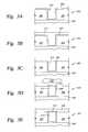
- FIGS. 3 a-eillustrate cross-sectional views of a wafer 301 at different stages of processing, including the post-CMP treatment according to one embodiment the invention.
- FIG. 3 ashows the wafer 301 comprising, for example, an insulating layer 305 that has been patterned to form a contact or via 307 .
- the underlying layer 303may comprise silicon, polysilicon, silicides, aluminum, tungsten, or other conducting or semiconducting materials.
- a barrier layer 309is also formed over the insulating layer 305 and inside the contact or via 307 .
- the barrier layer 309may, for example, be a combination layer comprising a refractory metal and a metal nitride—e.g., titanium and titanium nitride, tantalum and tantalum nitride, or tungsten and its nitride.
- the barrier layer 309is used to prevent undesirable diffusion of subsequently deposited metal into the underlying layer 303 .
- a copper layer 311is then formed on the barrier layer 309 , as shown in FIG. 3 b .
- the copper layer 311may be formed by either chemical vapor deposition (CVD), physical vapor deposition (PVD) or electroplating methods. If electroplating is used, then a seed layer (not shown) is formed prior to the electroplated copper layer 311 to facilitate electroplating.
- the copper layer 311 of FIG. 3 bis then subjected to planarization using CMP, in which at least a portion of the copper layer 311 is removed, resulting in a planarized structure comprising a polished copper layer 313 , as shown in FIG. 3 c .
- This polished copper layer 313may also be referred to as a copper feature.
- the wafer 301may be subjected to cleaning, rinsing or other processing steps (not shown in FIG. 3) after CMP.
- a post-CMP treatmentis performed on the wafer 301 , in which the wafer 301 is exposed to an electroless plating solution 350 , for example, at room temperature.
- an electroless plating solution 350for example, at room temperature.
- a metal-containing layer 315is deposited on the wafer 301 during the wafer cleaning with the electroless plating solution 350 .
- electroless depositioncan be performed by either spraying the electroless plating solution 350 onto the surface of the wafer 301 , or by immersing the wafer 301 in a bath containing the electroless plating solution 350 .
- the metal-containing layer 315may be nickel (Ni), tin (Sn), cobalt (Co), or alloys comprising different elements, e.g., cobalt tungsten phosphorus (CoWP).
- Ni and Snmay be deposited from solutions comprising the respective sulphate or chloride salts. Many other salts that are known in the art may also be used.
- Ronamerse 407a plating solution available from LeaRonal of New York, is also suitable for depositing Sn on copper features. Electroless deposition can be achieved in less than about 30 seconds at room temperature by immersing a wafer containing copper features in a bath containing the Ronamerse 407 solution at about 50% dilution with water. The deposited Sn layer can promote adhesion with a subsequently deposited layer such as an oxide layer.
- the metal-containing layer 315is Ni or CoWP, then the metal-containing layer 315 can act as both an adhesion layer and a barrier layer.
- the clean copper surfaceacts as a catalyst for electroless deposition.
- an appropriate reducing agent in the electroless plating solutione.g., one in which copper can catalyze a reduction reaction involving the reducing agent
- the metal-containing layer 315can be formed selectively on one or more copper features 313 of the wafer 301 .
- a hypophosphiteis a suitable reducing agent for use in electroless Ni deposition.
- the deposition timemay be adjusted to produce a metal-containing layer 315 having any desired thickness.
- the metal-containing layer 315is deposited to a thickness of less than about 1000 ⁇ , preferably between about 50 and about 100 ⁇ .
- a relatively thin metal-containing layer 315is preferred in order to avoid any excessive current passing through this metal-containing layer 315 during device operation. It is important, however, that the metal-containing layer 315 be formed as a continuous layer.
- a deposition time of less than about 30 seconds, or a few secondsis sufficient to provide a continuous metal-containing layer 315 .
- the deposition timecan be adjusted accordingly. For example, a deposition time of about 5 minutes may be used without significant impact on the process throughput.
- the resulting structuremay have improved properties such as reduced electromigration of the copper layer 313 , or enhanced adhesion of the insulating layer 320 .
- the post-CMP treatmenthas been used as one illustrative embodiment of the invention, the integrated cleaning/deposition can generally be applied to other stages of a processing sequence involving a variety of substrates and metal-containing layers that can be formed by electroless processes.
Landscapes
- Engineering & Computer Science (AREA)
- Physics & Mathematics (AREA)
- Condensed Matter Physics & Semiconductors (AREA)
- General Physics & Mathematics (AREA)
- Manufacturing & Machinery (AREA)
- Computer Hardware Design (AREA)
- Microelectronics & Electronic Packaging (AREA)
- Power Engineering (AREA)
- Internal Circuitry In Semiconductor Integrated Circuit Devices (AREA)
- Chemically Coating (AREA)
- Mechanical Treatment Of Semiconductor (AREA)
- Manufacturing Of Printed Wiring (AREA)
Abstract
Description
1. Field of the Invention
The invention relates to a method for substrate treatment.
2. Description of the Background Art
Copper and its alloys are increasingly being used for metal interconnects in advanced integrated circuit fabrication because they have lower resistivities compared to aluminum and do not suffer from poor electromigration. Copper can be deposited over high aspect ratio via and contact structures using metal electroplating. A typical electroplating method generally comprises vapor depositing a barrier layer over the via or contact, vapor depositing a conductive metal seed layer, e.g., copper, over the barrier layer, followed by electroplating a conductive metal over the seed layer to fill the via or contact structure. Finally, chemical mechanical polishing (CMP) can be used to define a planarized conductive interconnect feature by polishing the electroplated metal layer using a polishing fluid, which may include a chemical and an abrasive.
However, defects may be introduced into the planarized conductive layer after CMP. These defects may include, for example, particulate or chemical contamination, physical damage, discontinuity in the conductive layer, and so on. Therefore, the planarized metal layer is subjected to various post-CMP cleaning or treatment (e.g., thermal or plasma anneal) steps prior to additional processing such as subsequent deposition of a dielectric layer. However, even after post-CMP cleaning or treatment, the surface of the planarized layer may present other problems in subsequent processing—e.g., vulnerability to chemical corrosion, or failure to provide a good adhesive surface for a subsequently deposited layer such as a dielectric layer.
Therefore, there is an ongoing need for a method of post-CMP treatment of a metal layer.
The present invention generally provides a method of treating a substrate, comprising forming a metal-containing layer on the substrate during substrate cleaning. In one embodiment, a substrate is subjected to chemical mechanical polishing prior to being treated according to embodiments of the invention. During substrate cleaning following chemical mechanical polishing, the substrate is exposed to an electroless plating solution (or electrolyte) to form a metal-containing layer by electroless deposition over at least one portion of the substrate, e.g., over one or more copper features on the substrate. The electroless deposition of the metal-containing layer may be accomplished by either spraying the electroless plating solution on the substrate, or by immersing the substrate in a cleaning bath containing the electroless plating solution.
The teachings of the present invention can be readily understood by considering the following detailed description in conjunction with the accompanying drawings, in which:
FIG. 1 depicts an apparatus suitable for practicing the present invention;
FIG. 2 depicts a flow diagram illustrating chemical mechanical processing incorporating the present invention; and
FIGS. 3A-E depicts cross-sectional views of a wafer substrate during various stages of metal processing according to the present invention.
To facilitate understanding, identical reference numerals have been used, where possible, to designate identical elements that are common to the figures.
The present invention generally provides a method of treating a substrate by integrating the formation of a metal-containing layer on a substrate during a substrate cleaning process. In one aspect of the invention, an electroless deposition is incorporated into the cleaning process to form a metal-containing layer on the substrate. In one embodiment, the substrate comprises a copper layer that has been formed on a semiconductor wafer. As an illustration, the treatment method of the invention is performed on the copper layer after the wafer has been subjected to chemical mechanical polishing (CMP).
Apparatus
FIG. 1 illustrates a schematic diagram of anapparatus 100 suitable for practicing the treatment method of the present invention. For example, theapparatus 100 may be a Mirra Mesa™ CMP system, available commercially from Applied Materials, Inc., of Santa Clara, Calif. A description of the Mirra CMP system has been disclosed in commonly-assigned U.S. provisional patent application, entitled “Method and Apparatus For Transferring Semiconductor Wafers Using An Input Module,” Ser. No. 60/139,222, filed on Jun. 15, 1999, which is incorporated herein by reference.
TheCMP system 100 comprises apolisher 102, awet robot 104, acleaner 106, afactory interface module 108, and a plurality ofwafer cassettes 110.Robots 158 on thefactory interface module 108 are used to transport wafers between thecassettes 110 and thecleaner 106, while awet robot 104 and a CMP robot transport wafers between the input module and thevarious polishing stations 112. Typically, the CMP process begins by transporting a wafer to be polished from acassette 110 to theinput module 144. The wafer is then transported by thewet robot 104 to atransfer station 118, and subsequently, by means of arobot interface 116 and a CMP robot114, to one of thepolishing stations 112 for polishing. Once polishing is complete, the polished wafer is moved to thetransfer station 118 and delivered back to theinput module 144.
A conventional post-CMP cleaning sequence begins with the polished wafer being transported on a “walking beam”148 in acleaning section 138 of thecleaner 106. Thewalking beam 148, which comprises a series of wafer grippers (not shown) connected to a horizontal bar (not shown), transports polished wafers through different cleaning baths in thecleaning section 138. The wafer is washed and scrubbed with cleaning fluids as it moves through thecleaning section 138 on thewalking beam 148 towards anend 154 to remove the slurry and other contaminants which have accumulated on the wafer during polishing. At the end of the cleaning sequence, the cleaned wafer is removed from thewalking beam 148 by thefactory interface robot 158 and placed in one of thecassettes 110.
As illustrated in FIG. 1, thesystem 100 is also coupled to acontroller 180, which controls thesystem 100 for implementing the treatment method of the present invention. Illustratively, thecontroller 180 comprises a general purpose computer or a central processing unit (CPU)182,support circuitry 184, andmemories 186 containing associated control software. Thecontroller 180 is responsible for automated control of the numerous steps required for wafer processing—such as wafer transport, wafer polishing, temperature control, wafer cleaning, and so on. Bi-directional communications between thecontroller 180 and the various components of thesystem 100 are handled through numerous signal cables collectively referred to assignal buses 188, some of which are illustrated in FIG.1.
The method of the invention can also be practiced in an apparatus different from that illustrated in FIG. 1, e.g., a cleaning system having different cleaning modules such as a megasonic cleaner, scrubber and spin-rinse-dryer. For example, an electroless deposition may be incorporated as part of the megasonic clean step. Typically, the megasonic bath temperature is maintained at between about 25 and about 100° C. Details of this cleaning system are disclosed in commonly-assigned U.S. provisional patent application Ser. No. 60/131,124, entitled “Semiconductor Substrate Cleaning System,” filed on Apr. 27, 1999, which is incorporated herein by reference. In addition, embodiments according to the invention may also be performed in different spin-rinse-dryers, for example, by dispensing an electroless plating solution through a fluid delivery system adapted for rinsing operations. Depending on the desired metal-containing layer, different electroless plating solutions can be used. One example of a spin-rinse-dryer that is suitable for practicing the invention is disclosed in commonly-assigned U.S. patent application Ser. No. 09/350,212, entitled “Edge Bead Removal/Spin Rinse Dry (EBR/SRD) Module,” filed on Jul. 9, 1999, which is incorporated herein by reference.
Process
FIG. 2 illustrates a wafer process sequence incorporating a method of the invention. Instep 201, a wafer is subjected to CMP to produce a planarized structure. For example, the planarized structure may comprise a copper layer that has been deposited in a contact or via structure. According to one embodiment of the invention, the wafer is then subjected to apost-CMP treatment step 203. Thetreatment step 203 comprises cleaning the wafer and forming a metal-containing layer on the planarized structure of the polished wafer using an electroless process. The metal-containing layer may serve one or more functions—e.g., as an interface layer to improve adhesion between the copper layer and a subsequently deposited material layer, or as a barrier layer to minimize inter-diffusion between different material layers.
The metal-containing layer may be a single component metal layer, or it may be an alloy (or polyalloy) containing both metal and non-metal components. Examples include nickel, tin, cobalt, or cobalt tungsten phosphorus, among others. Different electroless plating solutions (or electrolytes) may be used for depositing the desired metal-containing layers, using process conditions that are known the art. An electroless plating solution usually comprises a water-soluble salt containing a metal to be deposited, along with other components such as a reducing agent, complexing agent, or stabilizer, among others. Examples of a reducing agent include hypophosphorous acid, water soluble hypophosphites such as sodium or potassium hypophosphite, among others. A complexing agent may include, for example, carboxylic acids such as malic acid, citric acid, or sodium salts of carboxylic acids, and others that are known in the art. In some applications such as electroless nickel plating, a stabilizer such as water-soluble lead salts, e.g., lead acetate, may also be added to the electroless plating solution. For example, nickel and tin may be deposited from their respective sulphate or chloride salts, and many other water-soluble salts containing the desired metallic ions can also be used in the electroless plating solution. Exemplary solutions and conditions for electroless plating nickel and tin may be found, for example, in Uchida et al., U.S. Pat. No. 5,910,340, issued on Jun. 8, 1999, and in Uchida et al., U.S. Pat. No. 5,248,527, issued on Sep. 28, 1993, both of which are incorporated herein by reference.
Furthermore, it is also possible to deposit an alloy containing a co-deposit of different elements by using an electroless solution containing suitable sources of these elements. For example, ternary alloys such as cobalt tungsten phosphorus (CoWP), may provide improved properties compared to other binary alloys. An electroless solution for depositing CoWP may contain, e.g., ammonium tungstenate as a source of tunngsten ions, cobalt chloride as a source of cobalt ions, hypophosphite as a reducing agent and a source of phosphorus ions, citrate as a complexing agent, and other additives such as pH adjuster and surfactant, among others. The deposition of electroless CoWP alloys on copper damascene structures has been disclosed by Lopatin et al., in “Thin Electroless barrier for Copper Films”, Proceedings of SPIE, Vol. 3508, pp.65-77 (September 1998), and is incorporated herein by reference.
Depending on the specific metals or alloys to be deposited, the concentrations and compositions of the electroless plating solutions to be used in embodiments of the invention may be adjusted as appropriate, using suitable parameter ranges known in the art. As an illustrative embodiment, nickel may be plated from an acidic nickel sulphate solution using sodium hypophosphite as a reducing agent. The solution may comprise about 87 g/l NiSO4.4H2O, 24 g/l Na2H2PO2.H2O, 30 g/l CH3COONa.3H2O, 4.1 g/l C3H4(OH)(COOH)3.H2O, 2 g/l NaO2C3H4COONa.6H2O, and 0.0015 g/l Pb(CH3COO)2.3H2O. In the case of tin (Sn) electroless deposition, a solution of a tin salt, thiourea and an acid may be used. Such a solution may comprise, for example, about 45 g/l of thiourea and 5 g/l of stannous chloride, SnCl2.2H2O, and sulphuric acid. The sulphuric acid concentration may vary between about 1 and about 100 g/l. The use of these solutions for the electroless plating of Ni and Sn on copper surfaces have been disclosed by Lin et al., in “Manufacturing of Cu/Electroless Nickel/Sn-Pb Flip Chip Solder Bumps”, IEEE Trans. Adv. Packaging, vol. 22, pp.575-579 (November 1999), and by Sullivan et al., U.S. Pat. No. 2,369,620, issued on Feb. 13, 1945, both of which are incorporated herein by reference. Typically, electroless deposition is performed at room temperature or above.
According to the invention, the formation of the metal-containing layer is integrated with the cleaning process of the substrate or wafer. The electroless plating solution is used during at least a part of the process to rinse the substrate. For example, substrate cleaning can be accomplished by spraying an electroless plating solution onto the copper surface as part of the cleaning sequence practiced in theapparatus 100. Particles or chemicals from the CMP slurry remaining on the substrate surface may be dislodged from the substrate by the spraying force. In another embodiment, the electroless plating solution can serve as a bath for both deposition and ultrasonic or megasonic cleaning. The substrate can be submerged in the electroless plating solution to rinse the substrate. In any case, the electroless plating solution serves a dual purpose—that of substrate cleaning as well as formation of a metal-containing layer.
The invention may be incorporated in different manners within a cleaning sequence, as shown in FIG.2. For example, the post-CMP treatment step203 (i.e., integrated cleaning and deposition) may be performed after an initial cleaning of the substrate. Aninitial cleaning step 211 may include spraying, ultrasonic or megasonic cleaning using a conventional cleaning fluid. As such, the integrated cleaning anddeposition step 203 of the invention provides a secondary cleaning function. In this embodiment, a relatively clean copper surface for electroless plating is provided, and a uniform deposition can be achieved. If a cleaning fluid, other than de-ionized water, is used in theinitial cleaning step 211, then the substrate is rinsed instep 213 with de-ionized water, in order to avoid possible undesirable reactions or contamination between the cleaning fluid and the plating solution. Alternatively, the substrate may also be cleaned and/or rinsed (sprayed or in ultrasonic or megasonic baths) initially insteps 211 and/or213 using de-ionized water prior to electroless plating. Depending on the applications, it may be desirable to perform additional processing of the substrate, as shown instep 215, prior to the cleaning anddeposition step 203. Such additional processing may, for example, include thermal anneal or plasma treatment of the copper layer or planarized structure on the wafer.
It is also possible that the integrated plating and cleaningstep 203 be performed without any initial cleaning or rinsingsteps
After thepost-CMP treatment step 203 of the invention, at least one rinsingstep 205 is performed to rinse off any residual electroless plating solution from the substrate surface. This rinsingstep 205 may be performed, for example, in a conventional spin-rinse-dryer. Additional processing is then performed on the substrate instep 207. Such processing may include, for example, additional film treatment such as thermal anneal or plasma treatment of the substrate, deposition of a dielectric layer on the treated substrate surface, and so on, that are used in the fabrication of semiconductor devices.
The integrated cleaning anddeposition step 203 improves the properties of the copper surface in one or more aspects. Adhesion between the copper and subsequently deposited material layer may be enhanced due to the substrate cleaning and/or the metal-containing layer serving as an interface, adhesion-promoting layer. Furthermore, the metal-containing layer deposited instep 203, e.g., Ni or CoWP, may serve as a barrier layer, thus reducing electromigration of copper or undesirable inter-diffusion between copper and the subsequently deposited layer.
FIGS. 3a-eillustrate cross-sectional views of awafer 301 at different stages of processing, including the post-CMP treatment according to one embodiment the invention. FIG. 3ashows thewafer 301 comprising, for example, an insulatinglayer 305 that has been patterned to form a contact or via307. In general, theunderlying layer 303 may comprise silicon, polysilicon, silicides, aluminum, tungsten, or other conducting or semiconducting materials. Typically, abarrier layer 309 is also formed over the insulatinglayer 305 and inside the contact or via307. Depending on the specific application, thebarrier layer 309 may, for example, be a combination layer comprising a refractory metal and a metal nitride—e.g., titanium and titanium nitride, tantalum and tantalum nitride, or tungsten and its nitride. Thebarrier layer 309 is used to prevent undesirable diffusion of subsequently deposited metal into theunderlying layer 303.
Acopper layer 311 is then formed on thebarrier layer 309, as shown in FIG. 3b. In general, thecopper layer 311 may be formed by either chemical vapor deposition (CVD), physical vapor deposition (PVD) or electroplating methods. If electroplating is used, then a seed layer (not shown) is formed prior to the electroplatedcopper layer 311 to facilitate electroplating. Thecopper layer 311 of FIG. 3bis then subjected to planarization using CMP, in which at least a portion of thecopper layer 311 is removed, resulting in a planarized structure comprising apolished copper layer 313, as shown in FIG. 3c. Thispolished copper layer 313 may also be referred to as a copper feature. As previously discussed in connection with FIG. 2, thewafer 301 may be subjected to cleaning, rinsing or other processing steps (not shown in FIG. 3) after CMP.
Thereafter, as shown in FIG. 3d, a post-CMP treatment is performed on thewafer 301, in which thewafer 301 is exposed to anelectroless plating solution 350, for example, at room temperature. According to embodiments of the invention, a metal-containinglayer 315 is deposited on thewafer 301 during the wafer cleaning with theelectroless plating solution 350. As previously explained, electroless deposition can be performed by either spraying theelectroless plating solution 350 onto the surface of thewafer 301, or by immersing thewafer 301 in a bath containing theelectroless plating solution 350. For example, the metal-containinglayer 315 may be nickel (Ni), tin (Sn), cobalt (Co), or alloys comprising different elements, e.g., cobalt tungsten phosphorus (CoWP). As previously discussed, Ni and Sn may be deposited from solutions comprising the respective sulphate or chloride salts. Many other salts that are known in the art may also be used. For example, Ronamerse407—a plating solution available from LeaRonal of New York, is also suitable for depositing Sn on copper features. Electroless deposition can be achieved in less than about 30 seconds at room temperature by immersing a wafer containing copper features in a bath containing the Ronamerse407 solution at about 50% dilution with water. The deposited Sn layer can promote adhesion with a subsequently deposited layer such as an oxide layer. When the metal-containinglayer 315 is Ni or CoWP, then the metal-containinglayer 315 can act as both an adhesion layer and a barrier layer.
According to one aspect of the invention, the clean copper surface acts as a catalyst for electroless deposition. By using an appropriate reducing agent in the electroless plating solution (e.g., one in which copper can catalyze a reduction reaction involving the reducing agent), the metal-containinglayer 315 can be formed selectively on one or more copper features313 of thewafer 301. For example, a hypophosphite is a suitable reducing agent for use in electroless Ni deposition. Furthermore, depending on the material used for thebarrier layer 309, it is also possible to have electroless deposition on thebarrier layer 309. As such, the metal-containinglayer 315 is not formed on the insulatinglayer 305 that has been exposed after the completion of CMP. Depending on the specific application and process needs, the deposition time may be adjusted to produce a metal-containinglayer 315 having any desired thickness. Typically, the metal-containinglayer 315 is deposited to a thickness of less than about 1000 Å, preferably between about 50 and about 100 Å. In general, a relatively thin metal-containinglayer 315 is preferred in order to avoid any excessive current passing through this metal-containinglayer 315 during device operation. It is important, however, that the metal-containinglayer 315 be formed as a continuous layer. Typically, a deposition time of less than about 30 seconds, or a few seconds, is sufficient to provide a continuous metal-containinglayer 315. Depending on the desired thickness or process throughput, the deposition time can be adjusted accordingly. For example, a deposition time of about 5 minutes may be used without significant impact on the process throughput.
After the formation of the metal-containinglayer 315 during the integrated cleaning/deposition treatment, processing continues for thewafer 301, e.g., with the deposition of an insulatinglayer 320, as shown in FIG. 3e. Depending on the specific properties of the metal-containinglayer 305, the resulting structure may have improved properties such as reduced electromigration of thecopper layer 313, or enhanced adhesion of the insulatinglayer 320. Although the post-CMP treatment has been used as one illustrative embodiment of the invention, the integrated cleaning/deposition can generally be applied to other stages of a processing sequence involving a variety of substrates and metal-containing layers that can be formed by electroless processes.
Although several preferred embodiments which incorporate the teachings of the present invention have been shown and described in detail, those skilled in the art can readily devise many other varied embodiments that still incorporate these teachings.
Claims (17)
1. A method for processing a substrate surface, comprising:
planarizing a substrate surface comprising a conductive material; and
forming a metal-containing layer on the substrate surface during substrate cleaning with a cleaning composition comprising an electroless plating solution, wherein forming the metal-containing layer comprises spraying the substrate surface with the cleaning composition to dislodge particles or chemicals remaining from the planarizing the substrate surface.
2. The method ofclaim 1 , wherein the planarizing a substrate surface forms a non-conductive surface comprising conductive features and the metal-containing layer selectively forms on the conductive features.
3. The method ofclaim 2 , wherein the conductive features comprise copper.
4. The method ofclaim 2 , wherein the metal-containing layer is formed by an electroless process.
5. The method ofclaim 1 , wherein the substrate surface is subjected to a cleaning process prior to forming the metal-containing layer on the substrate surface.
6. The method ofclaim 1 , wherein the substrate surface is rinsed with de-ionized water prior to forming the metal-containing layer on the substrate surface.
7. The method ofclaim 1 , wherein the metal-containing layer is selected from the group of nickel, tin, cobalt, cobalt tungsten phosphorus, and combinations thereof.
8. The method ofclaim 1 , wherein the electroless plating solution comprises a salt selected from the group of nickel sulphate and tin chloride.
9. The method ofclaim 1 , wherein the method steps for processing a substrate surface comprise a series of instructions disposed in a computer-readable medium adapted to implement instructions for processing the substrate by a chemical mechanical (CMP) system and cleaning apparatus when said instructions are arranged and executed by one or more processors connected to the chemical mechanical (CMP) system and cleaning apparatus.
10. A method of metal processing, comprising:
forming a first metal-containing layer on a substrate;
forming a planarized structure on the substrate by subjecting the first metal-containing layer to chemical mechanical polishing; and
forming a second metal-containing layer on the substrate during substrate cleaning with a cleaning composition comprises an electroless plating solution, wherein forming the second metal-containing layer comprises spraying the substrate with the cleaning composition to dislodge particles or chemicals remaining from the chemical mechanical polishing.
11. The method ofclaim 10 , wherein the forming a planarized structure on the substrate forms a non-conductive surface comprising conductive features and the metal-containing layer selectively forms on the conductive features.
12. The method ofclaim 11 , wherein the second metal-containing layer is formed by an electroless process.
13. The method ofclaim 11 , wherein the conductive features comprise copper.
14. The method ofclaim 10 , wherein.the second metal-containing layer is selected from the group of nickel, tin, cobalt, cobalt tungsten phosphorus, and combinations thereof.
15. The method ofclaim 10 , wherein the second metal-containing layer is a barrier layer.
16. The method ofclaim 10 , wherein the planarized structure formed by the chemical mechanical polishing is subjected to a cleaning process prior to forming the second metal-containing layer on the substrate.
17. The method ofclaim 16 , wherein the cleaning process comprises exposing the planarized structure to de-ionized water.
Priority Applications (3)
| Application Number | Priority Date | Filing Date | Title |
|---|---|---|---|
| US09/599,125US6645550B1 (en) | 2000-06-22 | 2000-06-22 | Method of treating a substrate |
| US09/850,841US6818066B2 (en) | 2000-06-22 | 2001-05-07 | Method and apparatus for treating a substrate |
| PCT/US2001/018733WO2001099173A2 (en) | 2000-06-22 | 2001-06-08 | Method of treating a substrate |
Applications Claiming Priority (1)
| Application Number | Priority Date | Filing Date | Title |
|---|---|---|---|
| US09/599,125US6645550B1 (en) | 2000-06-22 | 2000-06-22 | Method of treating a substrate |
Related Child Applications (1)
| Application Number | Title | Priority Date | Filing Date |
|---|---|---|---|
| US09/850,841Continuation-In-PartUS6818066B2 (en) | 2000-06-22 | 2001-05-07 | Method and apparatus for treating a substrate |
Publications (1)
| Publication Number | Publication Date |
|---|---|
| US6645550B1true US6645550B1 (en) | 2003-11-11 |
Family
ID=24398309
Family Applications (2)
| Application Number | Title | Priority Date | Filing Date |
|---|---|---|---|
| US09/599,125Expired - Fee RelatedUS6645550B1 (en) | 2000-06-22 | 2000-06-22 | Method of treating a substrate |
| US09/850,841Expired - Fee RelatedUS6818066B2 (en) | 2000-06-22 | 2001-05-07 | Method and apparatus for treating a substrate |
Family Applications After (1)
| Application Number | Title | Priority Date | Filing Date |
|---|---|---|---|
| US09/850,841Expired - Fee RelatedUS6818066B2 (en) | 2000-06-22 | 2001-05-07 | Method and apparatus for treating a substrate |
Country Status (2)
| Country | Link |
|---|---|
| US (2) | US6645550B1 (en) |
| WO (1) | WO2001099173A2 (en) |
Cited By (170)
| Publication number | Priority date | Publication date | Assignee | Title |
|---|---|---|---|---|
| US20030119317A1 (en)* | 2000-10-12 | 2003-06-26 | Takeshi Nogami | Semiconductor device and production method therefor |
| US20030190426A1 (en)* | 2002-04-03 | 2003-10-09 | Deenesh Padhi | Electroless deposition method |
| US20040005787A1 (en)* | 2002-07-02 | 2004-01-08 | Taiwan Semiconductor Manufacturing Co., Ltd. | Method to reduce residual particulate contamination in CVD and PVD semiconductor wafer manufacturing |
| US20040152318A1 (en)* | 2002-12-12 | 2004-08-05 | Dai Fukushima | Semiconductor device manufacturing method |
| US20040170766A1 (en)* | 2001-05-10 | 2004-09-02 | Hiroaki Inoue | Electroless plating method and device, and substrate processing method and apparatus |
| US20050081785A1 (en)* | 2003-10-15 | 2005-04-21 | Applied Materials, Inc. | Apparatus for electroless deposition |
| US20050164497A1 (en)* | 2004-01-26 | 2005-07-28 | Sergey Lopatin | Pretreatment for electroless deposition |
| US7064065B2 (en) | 2003-10-15 | 2006-06-20 | Applied Materials, Inc. | Silver under-layers for electroless cobalt alloys |
| US7205233B2 (en) | 2003-11-07 | 2007-04-17 | Applied Materials, Inc. | Method for forming CoWRe alloys by electroless deposition |
| US20070111519A1 (en)* | 2003-10-15 | 2007-05-17 | Applied Materials, Inc. | Integrated electroless deposition system |
| US20070128851A1 (en)* | 2001-01-05 | 2007-06-07 | Novellus Systems, Inc. | Fabrication of semiconductor interconnect structures |
| US20080156360A1 (en)* | 2006-12-26 | 2008-07-03 | Applied Materials, Inc. | Horizontal megasonic module for cleaning substrates |
| US7514353B2 (en) | 2005-03-18 | 2009-04-07 | Applied Materials, Inc. | Contact metallization scheme using a barrier layer over a silicide layer |
| US7651934B2 (en) | 2005-03-18 | 2010-01-26 | Applied Materials, Inc. | Process for electroless copper deposition |
| US7654221B2 (en) | 2003-10-06 | 2010-02-02 | Applied Materials, Inc. | Apparatus for electroless deposition of metals onto semiconductor substrates |
| US7659203B2 (en) | 2005-03-18 | 2010-02-09 | Applied Materials, Inc. | Electroless deposition process on a silicon contact |
| US7827930B2 (en) | 2004-01-26 | 2010-11-09 | Applied Materials, Inc. | Apparatus for electroless deposition of metals onto semiconductor substrates |
| US7867900B2 (en) | 2007-09-28 | 2011-01-11 | Applied Materials, Inc. | Aluminum contact integration on cobalt silicide junction |
| US8679983B2 (en) | 2011-09-01 | 2014-03-25 | Applied Materials, Inc. | Selective suppression of dry-etch rate of materials containing both silicon and nitrogen |
| US8679982B2 (en) | 2011-08-26 | 2014-03-25 | Applied Materials, Inc. | Selective suppression of dry-etch rate of materials containing both silicon and oxygen |
| US8765574B2 (en) | 2012-11-09 | 2014-07-01 | Applied Materials, Inc. | Dry etch process |
| US8771539B2 (en) | 2011-02-22 | 2014-07-08 | Applied Materials, Inc. | Remotely-excited fluorine and water vapor etch |
| US8801952B1 (en) | 2013-03-07 | 2014-08-12 | Applied Materials, Inc. | Conformal oxide dry etch |
| US8808563B2 (en) | 2011-10-07 | 2014-08-19 | Applied Materials, Inc. | Selective etch of silicon by way of metastable hydrogen termination |
| US8846163B2 (en) | 2004-02-26 | 2014-09-30 | Applied Materials, Inc. | Method for removing oxides |
| US8895449B1 (en) | 2013-05-16 | 2014-11-25 | Applied Materials, Inc. | Delicate dry clean |
| US8921234B2 (en) | 2012-12-21 | 2014-12-30 | Applied Materials, Inc. | Selective titanium nitride etching |
| US8927390B2 (en) | 2011-09-26 | 2015-01-06 | Applied Materials, Inc. | Intrench profile |
| US8951429B1 (en) | 2013-10-29 | 2015-02-10 | Applied Materials, Inc. | Tungsten oxide processing |
| US8956980B1 (en) | 2013-09-16 | 2015-02-17 | Applied Materials, Inc. | Selective etch of silicon nitride |
| US8969212B2 (en) | 2012-11-20 | 2015-03-03 | Applied Materials, Inc. | Dry-etch selectivity |
| US8975152B2 (en) | 2011-11-08 | 2015-03-10 | Applied Materials, Inc. | Methods of reducing substrate dislocation during gapfill processing |
| US8980763B2 (en) | 2012-11-30 | 2015-03-17 | Applied Materials, Inc. | Dry-etch for selective tungsten removal |
| US8999856B2 (en) | 2011-03-14 | 2015-04-07 | Applied Materials, Inc. | Methods for etch of sin films |
| US9023732B2 (en) | 2013-03-15 | 2015-05-05 | Applied Materials, Inc. | Processing systems and methods for halide scavenging |
| US9023734B2 (en) | 2012-09-18 | 2015-05-05 | Applied Materials, Inc. | Radical-component oxide etch |
| US9034770B2 (en) | 2012-09-17 | 2015-05-19 | Applied Materials, Inc. | Differential silicon oxide etch |
| US9040422B2 (en) | 2013-03-05 | 2015-05-26 | Applied Materials, Inc. | Selective titanium nitride removal |
| US9064815B2 (en) | 2011-03-14 | 2015-06-23 | Applied Materials, Inc. | Methods for etch of metal and metal-oxide films |
| US9064816B2 (en) | 2012-11-30 | 2015-06-23 | Applied Materials, Inc. | Dry-etch for selective oxidation removal |
| US9111877B2 (en) | 2012-12-18 | 2015-08-18 | Applied Materials, Inc. | Non-local plasma oxide etch |
| US9117855B2 (en) | 2013-12-04 | 2015-08-25 | Applied Materials, Inc. | Polarity control for remote plasma |
| US9114438B2 (en) | 2013-05-21 | 2015-08-25 | Applied Materials, Inc. | Copper residue chamber clean |
| US9136273B1 (en) | 2014-03-21 | 2015-09-15 | Applied Materials, Inc. | Flash gate air gap |
| US9132436B2 (en) | 2012-09-21 | 2015-09-15 | Applied Materials, Inc. | Chemical control features in wafer process equipment |
| US9159606B1 (en) | 2014-07-31 | 2015-10-13 | Applied Materials, Inc. | Metal air gap |
| US9165786B1 (en) | 2014-08-05 | 2015-10-20 | Applied Materials, Inc. | Integrated oxide and nitride recess for better channel contact in 3D architectures |
| US9190293B2 (en) | 2013-12-18 | 2015-11-17 | Applied Materials, Inc. | Even tungsten etch for high aspect ratio trenches |
| US9236266B2 (en) | 2011-08-01 | 2016-01-12 | Applied Materials, Inc. | Dry-etch for silicon-and-carbon-containing films |
| US9236265B2 (en) | 2013-11-04 | 2016-01-12 | Applied Materials, Inc. | Silicon germanium processing |
| US9245762B2 (en) | 2013-12-02 | 2016-01-26 | Applied Materials, Inc. | Procedure for etch rate consistency |
| US9263278B2 (en) | 2013-12-17 | 2016-02-16 | Applied Materials, Inc. | Dopant etch selectivity control |
| US9269590B2 (en) | 2014-04-07 | 2016-02-23 | Applied Materials, Inc. | Spacer formation |
| US9287095B2 (en) | 2013-12-17 | 2016-03-15 | Applied Materials, Inc. | Semiconductor system assemblies and methods of operation |
| US9287134B2 (en) | 2014-01-17 | 2016-03-15 | Applied Materials, Inc. | Titanium oxide etch |
| US9293568B2 (en) | 2014-01-27 | 2016-03-22 | Applied Materials, Inc. | Method of fin patterning |
| US9299537B2 (en) | 2014-03-20 | 2016-03-29 | Applied Materials, Inc. | Radial waveguide systems and methods for post-match control of microwaves |
| US9299538B2 (en) | 2014-03-20 | 2016-03-29 | Applied Materials, Inc. | Radial waveguide systems and methods for post-match control of microwaves |
| US9299583B1 (en) | 2014-12-05 | 2016-03-29 | Applied Materials, Inc. | Aluminum oxide selective etch |
| US9299575B2 (en) | 2014-03-17 | 2016-03-29 | Applied Materials, Inc. | Gas-phase tungsten etch |
| US9299582B2 (en) | 2013-11-12 | 2016-03-29 | Applied Materials, Inc. | Selective etch for metal-containing materials |
| US9309598B2 (en) | 2014-05-28 | 2016-04-12 | Applied Materials, Inc. | Oxide and metal removal |
| US9324576B2 (en) | 2010-05-27 | 2016-04-26 | Applied Materials, Inc. | Selective etch for silicon films |
| US9343272B1 (en) | 2015-01-08 | 2016-05-17 | Applied Materials, Inc. | Self-aligned process |
| US9349605B1 (en) | 2015-08-07 | 2016-05-24 | Applied Materials, Inc. | Oxide etch selectivity systems and methods |
| US9355862B2 (en) | 2014-09-24 | 2016-05-31 | Applied Materials, Inc. | Fluorine-based hardmask removal |
| US9355856B2 (en) | 2014-09-12 | 2016-05-31 | Applied Materials, Inc. | V trench dry etch |
| US9362130B2 (en) | 2013-03-01 | 2016-06-07 | Applied Materials, Inc. | Enhanced etching processes using remote plasma sources |
| US9368364B2 (en) | 2014-09-24 | 2016-06-14 | Applied Materials, Inc. | Silicon etch process with tunable selectivity to SiO2 and other materials |
| US9373517B2 (en) | 2012-08-02 | 2016-06-21 | Applied Materials, Inc. | Semiconductor processing with DC assisted RF power for improved control |
| US9373522B1 (en) | 2015-01-22 | 2016-06-21 | Applied Mateials, Inc. | Titanium nitride removal |
| US9378969B2 (en) | 2014-06-19 | 2016-06-28 | Applied Materials, Inc. | Low temperature gas-phase carbon removal |
| US9378978B2 (en) | 2014-07-31 | 2016-06-28 | Applied Materials, Inc. | Integrated oxide recess and floating gate fin trimming |
| US9385028B2 (en) | 2014-02-03 | 2016-07-05 | Applied Materials, Inc. | Air gap process |
| US9390937B2 (en) | 2012-09-20 | 2016-07-12 | Applied Materials, Inc. | Silicon-carbon-nitride selective etch |
| US9396989B2 (en) | 2014-01-27 | 2016-07-19 | Applied Materials, Inc. | Air gaps between copper lines |
| US9406523B2 (en) | 2014-06-19 | 2016-08-02 | Applied Materials, Inc. | Highly selective doped oxide removal method |
| US9425058B2 (en) | 2014-07-24 | 2016-08-23 | Applied Materials, Inc. | Simplified litho-etch-litho-etch process |
| US9449846B2 (en) | 2015-01-28 | 2016-09-20 | Applied Materials, Inc. | Vertical gate separation |
| US9478432B2 (en) | 2014-09-25 | 2016-10-25 | Applied Materials, Inc. | Silicon oxide selective removal |
| US9493879B2 (en) | 2013-07-12 | 2016-11-15 | Applied Materials, Inc. | Selective sputtering for pattern transfer |
| US9496167B2 (en) | 2014-07-31 | 2016-11-15 | Applied Materials, Inc. | Integrated bit-line airgap formation and gate stack post clean |
| US9499898B2 (en) | 2014-03-03 | 2016-11-22 | Applied Materials, Inc. | Layered thin film heater and method of fabrication |
| US9502258B2 (en) | 2014-12-23 | 2016-11-22 | Applied Materials, Inc. | Anisotropic gap etch |
| US9553102B2 (en) | 2014-08-19 | 2017-01-24 | Applied Materials, Inc. | Tungsten separation |
| US9576809B2 (en) | 2013-11-04 | 2017-02-21 | Applied Materials, Inc. | Etch suppression with germanium |
| US9659753B2 (en) | 2014-08-07 | 2017-05-23 | Applied Materials, Inc. | Grooved insulator to reduce leakage current |
| US9691645B2 (en) | 2015-08-06 | 2017-06-27 | Applied Materials, Inc. | Bolted wafer chuck thermal management systems and methods for wafer processing systems |
| US9721789B1 (en) | 2016-10-04 | 2017-08-01 | Applied Materials, Inc. | Saving ion-damaged spacers |
| US9728437B2 (en) | 2015-02-03 | 2017-08-08 | Applied Materials, Inc. | High temperature chuck for plasma processing systems |
| US9741593B2 (en) | 2015-08-06 | 2017-08-22 | Applied Materials, Inc. | Thermal management systems and methods for wafer processing systems |
| US9768034B1 (en) | 2016-11-11 | 2017-09-19 | Applied Materials, Inc. | Removal methods for high aspect ratio structures |
| US9773648B2 (en) | 2013-08-30 | 2017-09-26 | Applied Materials, Inc. | Dual discharge modes operation for remote plasma |
| US9847289B2 (en) | 2014-05-30 | 2017-12-19 | Applied Materials, Inc. | Protective via cap for improved interconnect performance |
| US9865484B1 (en) | 2016-06-29 | 2018-01-09 | Applied Materials, Inc. | Selective etch using material modification and RF pulsing |
| US9881805B2 (en) | 2015-03-02 | 2018-01-30 | Applied Materials, Inc. | Silicon selective removal |
| US9885117B2 (en) | 2014-03-31 | 2018-02-06 | Applied Materials, Inc. | Conditioned semiconductor system parts |
| US9934942B1 (en) | 2016-10-04 | 2018-04-03 | Applied Materials, Inc. | Chamber with flow-through source |
| US9947549B1 (en) | 2016-10-10 | 2018-04-17 | Applied Materials, Inc. | Cobalt-containing material removal |
| US10026621B2 (en) | 2016-11-14 | 2018-07-17 | Applied Materials, Inc. | SiN spacer profile patterning |
| US10043684B1 (en) | 2017-02-06 | 2018-08-07 | Applied Materials, Inc. | Self-limiting atomic thermal etching systems and methods |
| US10043674B1 (en) | 2017-08-04 | 2018-08-07 | Applied Materials, Inc. | Germanium etching systems and methods |
| US10049891B1 (en) | 2017-05-31 | 2018-08-14 | Applied Materials, Inc. | Selective in situ cobalt residue removal |
| US10062585B2 (en) | 2016-10-04 | 2018-08-28 | Applied Materials, Inc. | Oxygen compatible plasma source |
| US10062587B2 (en) | 2012-07-18 | 2018-08-28 | Applied Materials, Inc. | Pedestal with multi-zone temperature control and multiple purge capabilities |
| US10062579B2 (en) | 2016-10-07 | 2018-08-28 | Applied Materials, Inc. | Selective SiN lateral recess |
| US10062575B2 (en) | 2016-09-09 | 2018-08-28 | Applied Materials, Inc. | Poly directional etch by oxidation |
| US10128086B1 (en) | 2017-10-24 | 2018-11-13 | Applied Materials, Inc. | Silicon pretreatment for nitride removal |
| US10163696B2 (en) | 2016-11-11 | 2018-12-25 | Applied Materials, Inc. | Selective cobalt removal for bottom up gapfill |
| US10170282B2 (en) | 2013-03-08 | 2019-01-01 | Applied Materials, Inc. | Insulated semiconductor faceplate designs |
| US10170336B1 (en) | 2017-08-04 | 2019-01-01 | Applied Materials, Inc. | Methods for anisotropic control of selective silicon removal |
| US10224210B2 (en) | 2014-12-09 | 2019-03-05 | Applied Materials, Inc. | Plasma processing system with direct outlet toroidal plasma source |
| US10242908B2 (en) | 2016-11-14 | 2019-03-26 | Applied Materials, Inc. | Airgap formation with damage-free copper |
| US10256112B1 (en) | 2017-12-08 | 2019-04-09 | Applied Materials, Inc. | Selective tungsten removal |
| US10256079B2 (en) | 2013-02-08 | 2019-04-09 | Applied Materials, Inc. | Semiconductor processing systems having multiple plasma configurations |
| US10283324B1 (en) | 2017-10-24 | 2019-05-07 | Applied Materials, Inc. | Oxygen treatment for nitride etching |
| US10283321B2 (en) | 2011-01-18 | 2019-05-07 | Applied Materials, Inc. | Semiconductor processing system and methods using capacitively coupled plasma |
| US10297458B2 (en) | 2017-08-07 | 2019-05-21 | Applied Materials, Inc. | Process window widening using coated parts in plasma etch processes |
| US10319739B2 (en) | 2017-02-08 | 2019-06-11 | Applied Materials, Inc. | Accommodating imperfectly aligned memory holes |
| US10319649B2 (en) | 2017-04-11 | 2019-06-11 | Applied Materials, Inc. | Optical emission spectroscopy (OES) for remote plasma monitoring |
| US10319600B1 (en) | 2018-03-12 | 2019-06-11 | Applied Materials, Inc. | Thermal silicon etch |
| US10354889B2 (en) | 2017-07-17 | 2019-07-16 | Applied Materials, Inc. | Non-halogen etching of silicon-containing materials |
| US10403507B2 (en) | 2017-02-03 | 2019-09-03 | Applied Materials, Inc. | Shaped etch profile with oxidation |
| US10431429B2 (en) | 2017-02-03 | 2019-10-01 | Applied Materials, Inc. | Systems and methods for radial and azimuthal control of plasma uniformity |
| US10468267B2 (en) | 2017-05-31 | 2019-11-05 | Applied Materials, Inc. | Water-free etching methods |
| US10490418B2 (en) | 2014-10-14 | 2019-11-26 | Applied Materials, Inc. | Systems and methods for internal surface conditioning assessment in plasma processing equipment |
| US10490406B2 (en) | 2018-04-10 | 2019-11-26 | Appled Materials, Inc. | Systems and methods for material breakthrough |
| US10497573B2 (en) | 2018-03-13 | 2019-12-03 | Applied Materials, Inc. | Selective atomic layer etching of semiconductor materials |
| US10504700B2 (en) | 2015-08-27 | 2019-12-10 | Applied Materials, Inc. | Plasma etching systems and methods with secondary plasma injection |
| US10504754B2 (en) | 2016-05-19 | 2019-12-10 | Applied Materials, Inc. | Systems and methods for improved semiconductor etching and component protection |
| US10522371B2 (en) | 2016-05-19 | 2019-12-31 | Applied Materials, Inc. | Systems and methods for improved semiconductor etching and component protection |
| US10541184B2 (en) | 2017-07-11 | 2020-01-21 | Applied Materials, Inc. | Optical emission spectroscopic techniques for monitoring etching |
| US10541246B2 (en) | 2017-06-26 | 2020-01-21 | Applied Materials, Inc. | 3D flash memory cells which discourage cross-cell electrical tunneling |
| US10546729B2 (en) | 2016-10-04 | 2020-01-28 | Applied Materials, Inc. | Dual-channel showerhead with improved profile |
| US10566206B2 (en) | 2016-12-27 | 2020-02-18 | Applied Materials, Inc. | Systems and methods for anisotropic material breakthrough |
| US10573527B2 (en) | 2018-04-06 | 2020-02-25 | Applied Materials, Inc. | Gas-phase selective etching systems and methods |
| US10573496B2 (en) | 2014-12-09 | 2020-02-25 | Applied Materials, Inc. | Direct outlet toroidal plasma source |
| US10593523B2 (en) | 2014-10-14 | 2020-03-17 | Applied Materials, Inc. | Systems and methods for internal surface conditioning in plasma processing equipment |
| US10593560B2 (en) | 2018-03-01 | 2020-03-17 | Applied Materials, Inc. | Magnetic induction plasma source for semiconductor processes and equipment |
| US10615047B2 (en) | 2018-02-28 | 2020-04-07 | Applied Materials, Inc. | Systems and methods to form airgaps |
| US10629473B2 (en) | 2016-09-09 | 2020-04-21 | Applied Materials, Inc. | Footing removal for nitride spacer |
| US10672642B2 (en) | 2018-07-24 | 2020-06-02 | Applied Materials, Inc. | Systems and methods for pedestal configuration |
| US10679870B2 (en) | 2018-02-15 | 2020-06-09 | Applied Materials, Inc. | Semiconductor processing chamber multistage mixing apparatus |
| US10699879B2 (en) | 2018-04-17 | 2020-06-30 | Applied Materials, Inc. | Two piece electrode assembly with gap for plasma control |
| US10727080B2 (en) | 2017-07-07 | 2020-07-28 | Applied Materials, Inc. | Tantalum-containing material removal |
| US10755941B2 (en) | 2018-07-06 | 2020-08-25 | Applied Materials, Inc. | Self-limiting selective etching systems and methods |
| US10854426B2 (en) | 2018-01-08 | 2020-12-01 | Applied Materials, Inc. | Metal recess for semiconductor structures |
| US10872778B2 (en) | 2018-07-06 | 2020-12-22 | Applied Materials, Inc. | Systems and methods utilizing solid-phase etchants |
| US10886137B2 (en) | 2018-04-30 | 2021-01-05 | Applied Materials, Inc. | Selective nitride removal |
| US10892198B2 (en) | 2018-09-14 | 2021-01-12 | Applied Materials, Inc. | Systems and methods for improved performance in semiconductor processing |
| US10903054B2 (en) | 2017-12-19 | 2021-01-26 | Applied Materials, Inc. | Multi-zone gas distribution systems and methods |
| US10920319B2 (en) | 2019-01-11 | 2021-02-16 | Applied Materials, Inc. | Ceramic showerheads with conductive electrodes |
| US10920320B2 (en) | 2017-06-16 | 2021-02-16 | Applied Materials, Inc. | Plasma health determination in semiconductor substrate processing reactors |
| US10943834B2 (en) | 2017-03-13 | 2021-03-09 | Applied Materials, Inc. | Replacement contact process |
| US10964512B2 (en) | 2018-02-15 | 2021-03-30 | Applied Materials, Inc. | Semiconductor processing chamber multistage mixing apparatus and methods |
| US11049755B2 (en) | 2018-09-14 | 2021-06-29 | Applied Materials, Inc. | Semiconductor substrate supports with embedded RF shield |
| US11062887B2 (en) | 2018-09-17 | 2021-07-13 | Applied Materials, Inc. | High temperature RF heater pedestals |
| US11121002B2 (en) | 2018-10-24 | 2021-09-14 | Applied Materials, Inc. | Systems and methods for etching metals and metal derivatives |
| US11239061B2 (en) | 2014-11-26 | 2022-02-01 | Applied Materials, Inc. | Methods and systems to enhance process uniformity |
| US11257693B2 (en) | 2015-01-09 | 2022-02-22 | Applied Materials, Inc. | Methods and systems to improve pedestal temperature control |
| US11276590B2 (en) | 2017-05-17 | 2022-03-15 | Applied Materials, Inc. | Multi-zone semiconductor substrate supports |
| US11276559B2 (en) | 2017-05-17 | 2022-03-15 | Applied Materials, Inc. | Semiconductor processing chamber for multiple precursor flow |
| US11328909B2 (en) | 2017-12-22 | 2022-05-10 | Applied Materials, Inc. | Chamber conditioning and removal processes |
| US11417534B2 (en) | 2018-09-21 | 2022-08-16 | Applied Materials, Inc. | Selective material removal |
| US11437242B2 (en) | 2018-11-27 | 2022-09-06 | Applied Materials, Inc. | Selective removal of silicon-containing materials |
| US11594428B2 (en) | 2015-02-03 | 2023-02-28 | Applied Materials, Inc. | Low temperature chuck for plasma processing systems |
| US11682560B2 (en) | 2018-10-11 | 2023-06-20 | Applied Materials, Inc. | Systems and methods for hafnium-containing film removal |
| US11721527B2 (en) | 2019-01-07 | 2023-08-08 | Applied Materials, Inc. | Processing chamber mixing systems |
| US11749552B2 (en) | 2019-01-18 | 2023-09-05 | Applied Materials, Inc. | Wafer processing tools and methods thereof |
| US12340979B2 (en) | 2017-05-17 | 2025-06-24 | Applied Materials, Inc. | Semiconductor processing chamber for improved precursor flow |
Families Citing this family (25)
| Publication number | Priority date | Publication date | Assignee | Title |
|---|---|---|---|---|
| US7686935B2 (en)* | 1998-10-26 | 2010-03-30 | Novellus Systems, Inc. | Pad-assisted electropolishing |
| JP3902027B2 (en)* | 2002-03-01 | 2007-04-04 | 大日本スクリーン製造株式会社 | Substrate processing equipment |
| KR100473475B1 (en)* | 2002-08-09 | 2005-03-10 | 삼성전자주식회사 | Apparatus for cleaning a substrate |
| US8241701B2 (en)* | 2005-08-31 | 2012-08-14 | Lam Research Corporation | Processes and systems for engineering a barrier surface for copper deposition |
| US7413983B2 (en)* | 2003-06-13 | 2008-08-19 | Ebara Corporation | Plating method including pretreatment of a surface of a base metal |
| US7368017B2 (en)* | 2003-12-12 | 2008-05-06 | Lam Research Corporation | Method and apparatus for semiconductor wafer planarization |
| US8522799B2 (en)* | 2005-12-30 | 2013-09-03 | Lam Research Corporation | Apparatus and system for cleaning a substrate |
| US7183181B2 (en)* | 2004-09-27 | 2007-02-27 | Lsi Logic Corporation | Dynamic edge bead removal |
| WO2006055363A2 (en)* | 2004-11-12 | 2006-05-26 | Semitool, Inc. | Modular tool unit for processing microelectronic workpieces |
| US8211242B2 (en)* | 2005-02-07 | 2012-07-03 | Ebara Corporation | Substrate processing method, substrate processing apparatus, and control program |
| US7709873B2 (en)* | 2005-03-31 | 2010-05-04 | Intel Corporation | Polymer memory with adhesion layer containing an immobilized metal |
| JP4258663B2 (en)* | 2005-04-15 | 2009-04-30 | セイコーエプソン株式会社 | Coating apparatus and film forming apparatus |
| US20060246727A1 (en)* | 2005-04-27 | 2006-11-02 | Taiwan Semiconductor Manufacturing Company, Ltd. | Integrated dual damascene clean apparatus and process |
| US8771804B2 (en)* | 2005-08-31 | 2014-07-08 | Lam Research Corporation | Processes and systems for engineering a copper surface for selective metal deposition |
| US8747960B2 (en)* | 2005-08-31 | 2014-06-10 | Lam Research Corporation | Processes and systems for engineering a silicon-type surface for selective metal deposition to form a metal silicide |
| KR101506352B1 (en)* | 2006-08-30 | 2015-03-26 | 램 리써치 코포레이션 | Processes and integrated systems for processing substrate surfaces for metal deposition |
| US8226775B2 (en) | 2007-12-14 | 2012-07-24 | Lam Research Corporation | Methods for particle removal by single-phase and two-phase media |
| US8043976B2 (en)* | 2008-03-24 | 2011-10-25 | Air Products And Chemicals, Inc. | Adhesion to copper and copper electromigration resistance |
| CN102084466B (en)* | 2008-07-01 | 2013-09-11 | 应用材料公司 | Modular base-plate semiconductor polisher architecture |
| CN107799436B (en)* | 2016-08-29 | 2023-07-07 | 株式会社荏原制作所 | Substrate processing apparatus and substrate processing method |
| JP6971676B2 (en)* | 2016-08-29 | 2021-11-24 | 株式会社荏原製作所 | Board processing equipment and board processing method |
| US11682567B2 (en)* | 2020-06-30 | 2023-06-20 | Applied Materials, Inc. | Cleaning system with in-line SPM processing |
| US12198944B2 (en) | 2020-11-11 | 2025-01-14 | Applied Materials, Inc. | Substrate handling in a modular polishing system with single substrate cleaning chambers |
| US20220282918A1 (en) | 2021-03-03 | 2022-09-08 | Applied Materials, Inc. | Drying system with integrated substrate alignment stage |
| US20250140578A1 (en)* | 2023-10-27 | 2025-05-01 | Applied Materials, Inc. | Dio3 spray tank for post cmp substrate cleaning |
Citations (17)
| Publication number | Priority date | Publication date | Assignee | Title |
|---|---|---|---|---|
| US2369620A (en) | 1941-03-07 | 1945-02-13 | Battelle Development Corp | Method of coating cupreous metal with tin |
| US4232060A (en)* | 1979-01-22 | 1980-11-04 | Richardson Chemical Company | Method of preparing substrate surface for electroless plating and products produced thereby |
| US4368223A (en)* | 1981-06-01 | 1983-01-11 | Asahi Glass Company, Ltd. | Process for preparing nickel layer |
| US4397812A (en) | 1974-05-24 | 1983-08-09 | Richardson Chemical Company | Electroless nickel polyalloys |
| US4810520A (en)* | 1987-09-23 | 1989-03-07 | Magnetic Peripherals Inc. | Method for controlling electroless magnetic plating |
| US5147692A (en) | 1990-05-08 | 1992-09-15 | Macdermid, Incorporated | Electroless plating of nickel onto surfaces such as copper or fused tungston |
| US5248527A (en) | 1991-03-01 | 1993-09-28 | C. Uyemura And Company, Limited | Process for electroless plating tin, lead or tin-lead alloy |
| US5695810A (en) | 1996-11-20 | 1997-12-09 | Cornell Research Foundation, Inc. | Use of cobalt tungsten phosphide as a barrier material for copper metallization |
| US5843538A (en)* | 1996-12-09 | 1998-12-01 | John L. Raymond | Method for electroless nickel plating of metal substrates |
| US5904827A (en)* | 1996-10-15 | 1999-05-18 | Reynolds Tech Fabricators, Inc. | Plating cell with rotary wiper and megasonic transducer |
| US5910340A (en) | 1995-10-23 | 1999-06-08 | C. Uyemura & Co., Ltd. | Electroless nickel plating solution and method |
| US5969422A (en) | 1997-05-15 | 1999-10-19 | Advanced Micro Devices, Inc. | Plated copper interconnect structure |
| US6010962A (en) | 1999-02-12 | 2000-01-04 | Taiwan Semiconductor Manufacturing Company | Copper chemical-mechanical-polishing (CMP) dishing |
| US6015724A (en) | 1995-11-02 | 2000-01-18 | Semiconductor Energy Laboratory Co. | Manufacturing method of a semiconductor device |
| US6136693A (en) | 1997-10-27 | 2000-10-24 | Chartered Semiconductor Manufacturing Ltd. | Method for planarized interconnect vias using electroless plating and CMP |
| US6140234A (en) | 1998-01-20 | 2000-10-31 | International Business Machines Corporation | Method to selectively fill recesses with conductive metal |
| US6174812B1 (en) | 1999-06-08 | 2001-01-16 | United Microelectronics Corp. | Copper damascene technology for ultra large scale integration circuits |
Family Cites Families (20)
| Publication number | Priority date | Publication date | Assignee | Title |
|---|---|---|---|---|
| JP2655975B2 (en) | 1992-09-18 | 1997-09-24 | 三菱マテリアル株式会社 | Wafer polishing equipment |
| JP2839801B2 (en) | 1992-09-18 | 1998-12-16 | 三菱マテリアル株式会社 | Wafer manufacturing method |
| US5300155A (en) | 1992-12-23 | 1994-04-05 | Micron Semiconductor, Inc. | IC chemical mechanical planarization process incorporating slurry temperature control |
| US5895270A (en) | 1995-06-26 | 1999-04-20 | Texas Instruments Incorporated | Chemical mechanical polishing method and apparatus |
| KR100487590B1 (en) | 1995-08-21 | 2005-08-04 | 가부시키가이샤 에바라 세이사꾸쇼 | Polishing device |
| KR100209365B1 (en) | 1995-11-01 | 1999-07-15 | 김영환 | Manufacturing method of S.O.I semiconductor wafer |
| US5885134A (en) | 1996-04-18 | 1999-03-23 | Ebara Corporation | Polishing apparatus |
| TW419785B (en)* | 1996-11-28 | 2001-01-21 | Ind Tech Res Inst | Method and apparatus for forming very small scale metal interconnect on semiconductor substrates |
| US5922136A (en) | 1997-03-28 | 1999-07-13 | Taiwan Semiconductor Manufacturing Company, Ltd. | Post-CMP cleaner apparatus and method |
| AU8675798A (en)* | 1997-07-29 | 1999-02-22 | Silicon Genesis Corporation | Cluster tool method and apparatus using plasma immersion ion implantation |
| JP3788855B2 (en)* | 1997-09-11 | 2006-06-21 | 大日本スクリーン製造株式会社 | Substrate processing unit and substrate processing apparatus using the same |
| TW405158B (en)* | 1997-09-17 | 2000-09-11 | Ebara Corp | Plating apparatus for semiconductor wafer processing |
| US6110011A (en) | 1997-11-10 | 2000-08-29 | Applied Materials, Inc. | Integrated electrodeposition and chemical-mechanical polishing tool |
| US6000997A (en) | 1998-07-10 | 1999-12-14 | Aplex, Inc. | Temperature regulation in a CMP process |
| JP2000040679A (en)* | 1998-07-24 | 2000-02-08 | Hitachi Ltd | Method for manufacturing semiconductor integrated circuit device |
| US6150271A (en) | 1998-09-10 | 2000-11-21 | Lucent Technologies Inc. | Differential temperature control in chemical mechanical polishing processes |
| JP4212707B2 (en)* | 1998-11-26 | 2009-01-21 | スピードファム株式会社 | Wafer planarization system and wafer planarization method |
| US6066030A (en)* | 1999-03-04 | 2000-05-23 | International Business Machines Corporation | Electroetch and chemical mechanical polishing equipment |
| US6136163A (en) | 1999-03-05 | 2000-10-24 | Applied Materials, Inc. | Apparatus for electro-chemical deposition with thermal anneal chamber |
| JP2001023985A (en)* | 1999-07-08 | 2001-01-26 | Ebara Corp | Interconnection structure and preparation thereof |
- 2000
- 2000-06-22USUS09/599,125patent/US6645550B1/ennot_activeExpired - Fee Related
- 2001
- 2001-05-07USUS09/850,841patent/US6818066B2/ennot_activeExpired - Fee Related
- 2001-06-08WOPCT/US2001/018733patent/WO2001099173A2/enunknown
Patent Citations (17)
| Publication number | Priority date | Publication date | Assignee | Title |
|---|---|---|---|---|
| US2369620A (en) | 1941-03-07 | 1945-02-13 | Battelle Development Corp | Method of coating cupreous metal with tin |
| US4397812A (en) | 1974-05-24 | 1983-08-09 | Richardson Chemical Company | Electroless nickel polyalloys |
| US4232060A (en)* | 1979-01-22 | 1980-11-04 | Richardson Chemical Company | Method of preparing substrate surface for electroless plating and products produced thereby |
| US4368223A (en)* | 1981-06-01 | 1983-01-11 | Asahi Glass Company, Ltd. | Process for preparing nickel layer |
| US4810520A (en)* | 1987-09-23 | 1989-03-07 | Magnetic Peripherals Inc. | Method for controlling electroless magnetic plating |
| US5147692A (en) | 1990-05-08 | 1992-09-15 | Macdermid, Incorporated | Electroless plating of nickel onto surfaces such as copper or fused tungston |
| US5248527A (en) | 1991-03-01 | 1993-09-28 | C. Uyemura And Company, Limited | Process for electroless plating tin, lead or tin-lead alloy |
| US5910340A (en) | 1995-10-23 | 1999-06-08 | C. Uyemura & Co., Ltd. | Electroless nickel plating solution and method |
| US6015724A (en) | 1995-11-02 | 2000-01-18 | Semiconductor Energy Laboratory Co. | Manufacturing method of a semiconductor device |
| US5904827A (en)* | 1996-10-15 | 1999-05-18 | Reynolds Tech Fabricators, Inc. | Plating cell with rotary wiper and megasonic transducer |
| US5695810A (en) | 1996-11-20 | 1997-12-09 | Cornell Research Foundation, Inc. | Use of cobalt tungsten phosphide as a barrier material for copper metallization |
| US5843538A (en)* | 1996-12-09 | 1998-12-01 | John L. Raymond | Method for electroless nickel plating of metal substrates |
| US5969422A (en) | 1997-05-15 | 1999-10-19 | Advanced Micro Devices, Inc. | Plated copper interconnect structure |
| US6136693A (en) | 1997-10-27 | 2000-10-24 | Chartered Semiconductor Manufacturing Ltd. | Method for planarized interconnect vias using electroless plating and CMP |
| US6140234A (en) | 1998-01-20 | 2000-10-31 | International Business Machines Corporation | Method to selectively fill recesses with conductive metal |
| US6010962A (en) | 1999-02-12 | 2000-01-04 | Taiwan Semiconductor Manufacturing Company | Copper chemical-mechanical-polishing (CMP) dishing |
| US6174812B1 (en) | 1999-06-08 | 2001-01-16 | United Microelectronics Corp. | Copper damascene technology for ultra large scale integration circuits |
Non-Patent Citations (3)
| Title |
|---|
| Lin et al. "Manufacturing of Cu/Electroless Nickel/Sn-Pb Flip Chip Solder Bumps" , IEEE Transactions on Advanced Packaging, vol. 22, No. 4,pp. 575-579, Nov. 1999. |
| Lopatin et al. "Thin Electroless Barrier for Copper Films" Part of the SPIE Conference of Multilevel Interconnect Technology II, SPIE vol. 3508, pp. 65-77, 1998. |
| Lopatin et al., "Thin Electroless Barrier for Copper Films", Multilevel Interconnect Technology II, Proceedings of SPIE, vol. 3508, pp. 65-77, Sep. 1998.** |
Cited By (249)
| Publication number | Priority date | Publication date | Assignee | Title |
|---|---|---|---|---|
| US6878632B2 (en)* | 2000-10-12 | 2005-04-12 | Sony Corporation | Semiconductor device having a conductive layer with a cobalt tungsten phosphorus coating and a manufacturing method thereof |
| US20030119317A1 (en)* | 2000-10-12 | 2003-06-26 | Takeshi Nogami | Semiconductor device and production method therefor |
| US20070128851A1 (en)* | 2001-01-05 | 2007-06-07 | Novellus Systems, Inc. | Fabrication of semiconductor interconnect structures |
| US20040170766A1 (en)* | 2001-05-10 | 2004-09-02 | Hiroaki Inoue | Electroless plating method and device, and substrate processing method and apparatus |
| US20030190426A1 (en)* | 2002-04-03 | 2003-10-09 | Deenesh Padhi | Electroless deposition method |
| US20040005787A1 (en)* | 2002-07-02 | 2004-01-08 | Taiwan Semiconductor Manufacturing Co., Ltd. | Method to reduce residual particulate contamination in CVD and PVD semiconductor wafer manufacturing |
| US6812156B2 (en)* | 2002-07-02 | 2004-11-02 | Taiwan Semiconductor Manufacturing Co., Ltd | Method to reduce residual particulate contamination in CVD and PVD semiconductor wafer manufacturing |
| US20040152318A1 (en)* | 2002-12-12 | 2004-08-05 | Dai Fukushima | Semiconductor device manufacturing method |
| US6984582B2 (en)* | 2002-12-12 | 2006-01-10 | Kabushiki Kaisha Toshiba | Method of making semiconductor device by polishing with intermediate clean polishing |
| US7654221B2 (en) | 2003-10-06 | 2010-02-02 | Applied Materials, Inc. | Apparatus for electroless deposition of metals onto semiconductor substrates |
| US7064065B2 (en) | 2003-10-15 | 2006-06-20 | Applied Materials, Inc. | Silver under-layers for electroless cobalt alloys |
| US20070111519A1 (en)* | 2003-10-15 | 2007-05-17 | Applied Materials, Inc. | Integrated electroless deposition system |
| US7341633B2 (en) | 2003-10-15 | 2008-03-11 | Applied Materials, Inc. | Apparatus for electroless deposition |
| US20050081785A1 (en)* | 2003-10-15 | 2005-04-21 | Applied Materials, Inc. | Apparatus for electroless deposition |
| US7205233B2 (en) | 2003-11-07 | 2007-04-17 | Applied Materials, Inc. | Method for forming CoWRe alloys by electroless deposition |
| US7256111B2 (en) | 2004-01-26 | 2007-08-14 | Applied Materials, Inc. | Pretreatment for electroless deposition |
| US20050164497A1 (en)* | 2004-01-26 | 2005-07-28 | Sergey Lopatin | Pretreatment for electroless deposition |
| US7827930B2 (en) | 2004-01-26 | 2010-11-09 | Applied Materials, Inc. | Apparatus for electroless deposition of metals onto semiconductor substrates |
| US8846163B2 (en) | 2004-02-26 | 2014-09-30 | Applied Materials, Inc. | Method for removing oxides |
| US8308858B2 (en) | 2005-03-18 | 2012-11-13 | Applied Materials, Inc. | Electroless deposition process on a silicon contact |
| US7514353B2 (en) | 2005-03-18 | 2009-04-07 | Applied Materials, Inc. | Contact metallization scheme using a barrier layer over a silicide layer |
| US7651934B2 (en) | 2005-03-18 | 2010-01-26 | Applied Materials, Inc. | Process for electroless copper deposition |
| US7659203B2 (en) | 2005-03-18 | 2010-02-09 | Applied Materials, Inc. | Electroless deposition process on a silicon contact |
| US20080156360A1 (en)* | 2006-12-26 | 2008-07-03 | Applied Materials, Inc. | Horizontal megasonic module for cleaning substrates |
| US7867900B2 (en) | 2007-09-28 | 2011-01-11 | Applied Materials, Inc. | Aluminum contact integration on cobalt silicide junction |
| US9324576B2 (en) | 2010-05-27 | 2016-04-26 | Applied Materials, Inc. | Selective etch for silicon films |
| US9754800B2 (en) | 2010-05-27 | 2017-09-05 | Applied Materials, Inc. | Selective etch for silicon films |
| US10283321B2 (en) | 2011-01-18 | 2019-05-07 | Applied Materials, Inc. | Semiconductor processing system and methods using capacitively coupled plasma |
| US8771539B2 (en) | 2011-02-22 | 2014-07-08 | Applied Materials, Inc. | Remotely-excited fluorine and water vapor etch |
| US10062578B2 (en) | 2011-03-14 | 2018-08-28 | Applied Materials, Inc. | Methods for etch of metal and metal-oxide films |
| US8999856B2 (en) | 2011-03-14 | 2015-04-07 | Applied Materials, Inc. | Methods for etch of sin films |
| US9842744B2 (en) | 2011-03-14 | 2017-12-12 | Applied Materials, Inc. | Methods for etch of SiN films |
| US9064815B2 (en) | 2011-03-14 | 2015-06-23 | Applied Materials, Inc. | Methods for etch of metal and metal-oxide films |
| US9236266B2 (en) | 2011-08-01 | 2016-01-12 | Applied Materials, Inc. | Dry-etch for silicon-and-carbon-containing films |
| US8679982B2 (en) | 2011-08-26 | 2014-03-25 | Applied Materials, Inc. | Selective suppression of dry-etch rate of materials containing both silicon and oxygen |
| US8679983B2 (en) | 2011-09-01 | 2014-03-25 | Applied Materials, Inc. | Selective suppression of dry-etch rate of materials containing both silicon and nitrogen |
| US8927390B2 (en) | 2011-09-26 | 2015-01-06 | Applied Materials, Inc. | Intrench profile |
| US9012302B2 (en) | 2011-09-26 | 2015-04-21 | Applied Materials, Inc. | Intrench profile |
| US9418858B2 (en) | 2011-10-07 | 2016-08-16 | Applied Materials, Inc. | Selective etch of silicon by way of metastable hydrogen termination |
| US8808563B2 (en) | 2011-10-07 | 2014-08-19 | Applied Materials, Inc. | Selective etch of silicon by way of metastable hydrogen termination |
| US8975152B2 (en) | 2011-11-08 | 2015-03-10 | Applied Materials, Inc. | Methods of reducing substrate dislocation during gapfill processing |
| US10062587B2 (en) | 2012-07-18 | 2018-08-28 | Applied Materials, Inc. | Pedestal with multi-zone temperature control and multiple purge capabilities |
| US9373517B2 (en) | 2012-08-02 | 2016-06-21 | Applied Materials, Inc. | Semiconductor processing with DC assisted RF power for improved control |
| US10032606B2 (en) | 2012-08-02 | 2018-07-24 | Applied Materials, Inc. | Semiconductor processing with DC assisted RF power for improved control |
| US9034770B2 (en) | 2012-09-17 | 2015-05-19 | Applied Materials, Inc. | Differential silicon oxide etch |
| US9887096B2 (en) | 2012-09-17 | 2018-02-06 | Applied Materials, Inc. | Differential silicon oxide etch |
| US9023734B2 (en) | 2012-09-18 | 2015-05-05 | Applied Materials, Inc. | Radical-component oxide etch |
| US9437451B2 (en) | 2012-09-18 | 2016-09-06 | Applied Materials, Inc. | Radical-component oxide etch |
| US9390937B2 (en) | 2012-09-20 | 2016-07-12 | Applied Materials, Inc. | Silicon-carbon-nitride selective etch |
| US9978564B2 (en) | 2012-09-21 | 2018-05-22 | Applied Materials, Inc. | Chemical control features in wafer process equipment |
| US10354843B2 (en) | 2012-09-21 | 2019-07-16 | Applied Materials, Inc. | Chemical control features in wafer process equipment |
| US11264213B2 (en) | 2012-09-21 | 2022-03-01 | Applied Materials, Inc. | Chemical control features in wafer process equipment |
| US9132436B2 (en) | 2012-09-21 | 2015-09-15 | Applied Materials, Inc. | Chemical control features in wafer process equipment |
| US8765574B2 (en) | 2012-11-09 | 2014-07-01 | Applied Materials, Inc. | Dry etch process |
| US9384997B2 (en) | 2012-11-20 | 2016-07-05 | Applied Materials, Inc. | Dry-etch selectivity |
| US8969212B2 (en) | 2012-11-20 | 2015-03-03 | Applied Materials, Inc. | Dry-etch selectivity |
| US8980763B2 (en) | 2012-11-30 | 2015-03-17 | Applied Materials, Inc. | Dry-etch for selective tungsten removal |
| US9412608B2 (en) | 2012-11-30 | 2016-08-09 | Applied Materials, Inc. | Dry-etch for selective tungsten removal |
| US9064816B2 (en) | 2012-11-30 | 2015-06-23 | Applied Materials, Inc. | Dry-etch for selective oxidation removal |
| US9111877B2 (en) | 2012-12-18 | 2015-08-18 | Applied Materials, Inc. | Non-local plasma oxide etch |
| US9355863B2 (en) | 2012-12-18 | 2016-05-31 | Applied Materials, Inc. | Non-local plasma oxide etch |
| US9449845B2 (en) | 2012-12-21 | 2016-09-20 | Applied Materials, Inc. | Selective titanium nitride etching |
| US8921234B2 (en) | 2012-12-21 | 2014-12-30 | Applied Materials, Inc. | Selective titanium nitride etching |
| US10256079B2 (en) | 2013-02-08 | 2019-04-09 | Applied Materials, Inc. | Semiconductor processing systems having multiple plasma configurations |
| US11024486B2 (en) | 2013-02-08 | 2021-06-01 | Applied Materials, Inc. | Semiconductor processing systems having multiple plasma configurations |
| US9362130B2 (en) | 2013-03-01 | 2016-06-07 | Applied Materials, Inc. | Enhanced etching processes using remote plasma sources |
| US10424485B2 (en) | 2013-03-01 | 2019-09-24 | Applied Materials, Inc. | Enhanced etching processes using remote plasma sources |
| US9607856B2 (en) | 2013-03-05 | 2017-03-28 | Applied Materials, Inc. | Selective titanium nitride removal |
| US9040422B2 (en) | 2013-03-05 | 2015-05-26 | Applied Materials, Inc. | Selective titanium nitride removal |
| US9093390B2 (en) | 2013-03-07 | 2015-07-28 | Applied Materials, Inc. | Conformal oxide dry etch |
| US8801952B1 (en) | 2013-03-07 | 2014-08-12 | Applied Materials, Inc. | Conformal oxide dry etch |
| US10170282B2 (en) | 2013-03-08 | 2019-01-01 | Applied Materials, Inc. | Insulated semiconductor faceplate designs |
| US9093371B2 (en) | 2013-03-15 | 2015-07-28 | Applied Materials, Inc. | Processing systems and methods for halide scavenging |
| US9704723B2 (en) | 2013-03-15 | 2017-07-11 | Applied Materials, Inc. | Processing systems and methods for halide scavenging |
| US9991134B2 (en) | 2013-03-15 | 2018-06-05 | Applied Materials, Inc. | Processing systems and methods for halide scavenging |
| US9659792B2 (en) | 2013-03-15 | 2017-05-23 | Applied Materials, Inc. | Processing systems and methods for halide scavenging |
| US9449850B2 (en) | 2013-03-15 | 2016-09-20 | Applied Materials, Inc. | Processing systems and methods for halide scavenging |
| US9184055B2 (en) | 2013-03-15 | 2015-11-10 | Applied Materials, Inc. | Processing systems and methods for halide scavenging |
| US9023732B2 (en) | 2013-03-15 | 2015-05-05 | Applied Materials, Inc. | Processing systems and methods for halide scavenging |
| US9153442B2 (en) | 2013-03-15 | 2015-10-06 | Applied Materials, Inc. | Processing systems and methods for halide scavenging |
| US8895449B1 (en) | 2013-05-16 | 2014-11-25 | Applied Materials, Inc. | Delicate dry clean |
| US9114438B2 (en) | 2013-05-21 | 2015-08-25 | Applied Materials, Inc. | Copper residue chamber clean |
| US9493879B2 (en) | 2013-07-12 | 2016-11-15 | Applied Materials, Inc. | Selective sputtering for pattern transfer |
| US9773648B2 (en) | 2013-08-30 | 2017-09-26 | Applied Materials, Inc. | Dual discharge modes operation for remote plasma |
| US8956980B1 (en) | 2013-09-16 | 2015-02-17 | Applied Materials, Inc. | Selective etch of silicon nitride |
| US9209012B2 (en) | 2013-09-16 | 2015-12-08 | Applied Materials, Inc. | Selective etch of silicon nitride |
| US8951429B1 (en) | 2013-10-29 | 2015-02-10 | Applied Materials, Inc. | Tungsten oxide processing |
| US9576809B2 (en) | 2013-11-04 | 2017-02-21 | Applied Materials, Inc. | Etch suppression with germanium |
| US9236265B2 (en) | 2013-11-04 | 2016-01-12 | Applied Materials, Inc. | Silicon germanium processing |
| US9299582B2 (en) | 2013-11-12 | 2016-03-29 | Applied Materials, Inc. | Selective etch for metal-containing materials |
| US9711366B2 (en) | 2013-11-12 | 2017-07-18 | Applied Materials, Inc. | Selective etch for metal-containing materials |
| US9472417B2 (en) | 2013-11-12 | 2016-10-18 | Applied Materials, Inc. | Plasma-free metal etch |
| US9520303B2 (en) | 2013-11-12 | 2016-12-13 | Applied Materials, Inc. | Aluminum selective etch |
| US9245762B2 (en) | 2013-12-02 | 2016-01-26 | Applied Materials, Inc. | Procedure for etch rate consistency |
| US9472412B2 (en) | 2013-12-02 | 2016-10-18 | Applied Materials, Inc. | Procedure for etch rate consistency |
| US9117855B2 (en) | 2013-12-04 | 2015-08-25 | Applied Materials, Inc. | Polarity control for remote plasma |
| US9287095B2 (en) | 2013-12-17 | 2016-03-15 | Applied Materials, Inc. | Semiconductor system assemblies and methods of operation |
| US9263278B2 (en) | 2013-12-17 | 2016-02-16 | Applied Materials, Inc. | Dopant etch selectivity control |
| US9190293B2 (en) | 2013-12-18 | 2015-11-17 | Applied Materials, Inc. | Even tungsten etch for high aspect ratio trenches |
| US9287134B2 (en) | 2014-01-17 | 2016-03-15 | Applied Materials, Inc. | Titanium oxide etch |
| US9396989B2 (en) | 2014-01-27 | 2016-07-19 | Applied Materials, Inc. | Air gaps between copper lines |
| US9293568B2 (en) | 2014-01-27 | 2016-03-22 | Applied Materials, Inc. | Method of fin patterning |
| US9385028B2 (en) | 2014-02-03 | 2016-07-05 | Applied Materials, Inc. | Air gap process |
| US9499898B2 (en) | 2014-03-03 | 2016-11-22 | Applied Materials, Inc. | Layered thin film heater and method of fabrication |
| US9299575B2 (en) | 2014-03-17 | 2016-03-29 | Applied Materials, Inc. | Gas-phase tungsten etch |
| US9564296B2 (en) | 2014-03-20 | 2017-02-07 | Applied Materials, Inc. | Radial waveguide systems and methods for post-match control of microwaves |
| US9299537B2 (en) | 2014-03-20 | 2016-03-29 | Applied Materials, Inc. | Radial waveguide systems and methods for post-match control of microwaves |
| US9299538B2 (en) | 2014-03-20 | 2016-03-29 | Applied Materials, Inc. | Radial waveguide systems and methods for post-match control of microwaves |
| US9837249B2 (en) | 2014-03-20 | 2017-12-05 | Applied Materials, Inc. | Radial waveguide systems and methods for post-match control of microwaves |
| US9136273B1 (en) | 2014-03-21 | 2015-09-15 | Applied Materials, Inc. | Flash gate air gap |
| US9903020B2 (en) | 2014-03-31 | 2018-02-27 | Applied Materials, Inc. | Generation of compact alumina passivation layers on aluminum plasma equipment components |
| US9885117B2 (en) | 2014-03-31 | 2018-02-06 | Applied Materials, Inc. | Conditioned semiconductor system parts |
| US9269590B2 (en) | 2014-04-07 | 2016-02-23 | Applied Materials, Inc. | Spacer formation |
| US10465294B2 (en) | 2014-05-28 | 2019-11-05 | Applied Materials, Inc. | Oxide and metal removal |
| US9309598B2 (en) | 2014-05-28 | 2016-04-12 | Applied Materials, Inc. | Oxide and metal removal |
| US9847289B2 (en) | 2014-05-30 | 2017-12-19 | Applied Materials, Inc. | Protective via cap for improved interconnect performance |
| US9378969B2 (en) | 2014-06-19 | 2016-06-28 | Applied Materials, Inc. | Low temperature gas-phase carbon removal |
| US9406523B2 (en) | 2014-06-19 | 2016-08-02 | Applied Materials, Inc. | Highly selective doped oxide removal method |
| US9425058B2 (en) | 2014-07-24 | 2016-08-23 | Applied Materials, Inc. | Simplified litho-etch-litho-etch process |
| US9773695B2 (en) | 2014-07-31 | 2017-09-26 | Applied Materials, Inc. | Integrated bit-line airgap formation and gate stack post clean |
| US9159606B1 (en) | 2014-07-31 | 2015-10-13 | Applied Materials, Inc. | Metal air gap |
| US9378978B2 (en) | 2014-07-31 | 2016-06-28 | Applied Materials, Inc. | Integrated oxide recess and floating gate fin trimming |
| US9496167B2 (en) | 2014-07-31 | 2016-11-15 | Applied Materials, Inc. | Integrated bit-line airgap formation and gate stack post clean |
| US9165786B1 (en) | 2014-08-05 | 2015-10-20 | Applied Materials, Inc. | Integrated oxide and nitride recess for better channel contact in 3D architectures |
| US9659753B2 (en) | 2014-08-07 | 2017-05-23 | Applied Materials, Inc. | Grooved insulator to reduce leakage current |
| US9553102B2 (en) | 2014-08-19 | 2017-01-24 | Applied Materials, Inc. | Tungsten separation |
| US9355856B2 (en) | 2014-09-12 | 2016-05-31 | Applied Materials, Inc. | V trench dry etch |
| US9355862B2 (en) | 2014-09-24 | 2016-05-31 | Applied Materials, Inc. | Fluorine-based hardmask removal |
| US9368364B2 (en) | 2014-09-24 | 2016-06-14 | Applied Materials, Inc. | Silicon etch process with tunable selectivity to SiO2 and other materials |
| US9478434B2 (en) | 2014-09-24 | 2016-10-25 | Applied Materials, Inc. | Chlorine-based hardmask removal |
| US9478432B2 (en) | 2014-09-25 | 2016-10-25 | Applied Materials, Inc. | Silicon oxide selective removal |
| US9613822B2 (en) | 2014-09-25 | 2017-04-04 | Applied Materials, Inc. | Oxide etch selectivity enhancement |
| US9837284B2 (en) | 2014-09-25 | 2017-12-05 | Applied Materials, Inc. | Oxide etch selectivity enhancement |
| US10490418B2 (en) | 2014-10-14 | 2019-11-26 | Applied Materials, Inc. | Systems and methods for internal surface conditioning assessment in plasma processing equipment |
| US10593523B2 (en) | 2014-10-14 | 2020-03-17 | Applied Materials, Inc. | Systems and methods for internal surface conditioning in plasma processing equipment |
| US10707061B2 (en) | 2014-10-14 | 2020-07-07 | Applied Materials, Inc. | Systems and methods for internal surface conditioning in plasma processing equipment |
| US10796922B2 (en) | 2014-10-14 | 2020-10-06 | Applied Materials, Inc. | Systems and methods for internal surface conditioning assessment in plasma processing equipment |
| US11239061B2 (en) | 2014-11-26 | 2022-02-01 | Applied Materials, Inc. | Methods and systems to enhance process uniformity |
| US11637002B2 (en) | 2014-11-26 | 2023-04-25 | Applied Materials, Inc. | Methods and systems to enhance process uniformity |
| US9299583B1 (en) | 2014-12-05 | 2016-03-29 | Applied Materials, Inc. | Aluminum oxide selective etch |
| US10573496B2 (en) | 2014-12-09 | 2020-02-25 | Applied Materials, Inc. | Direct outlet toroidal plasma source |
| US10224210B2 (en) | 2014-12-09 | 2019-03-05 | Applied Materials, Inc. | Plasma processing system with direct outlet toroidal plasma source |
| US9502258B2 (en) | 2014-12-23 | 2016-11-22 | Applied Materials, Inc. | Anisotropic gap etch |
| US9343272B1 (en) | 2015-01-08 | 2016-05-17 | Applied Materials, Inc. | Self-aligned process |
| US11257693B2 (en) | 2015-01-09 | 2022-02-22 | Applied Materials, Inc. | Methods and systems to improve pedestal temperature control |
| US9373522B1 (en) | 2015-01-22 | 2016-06-21 | Applied Mateials, Inc. | Titanium nitride removal |
| US9449846B2 (en) | 2015-01-28 | 2016-09-20 | Applied Materials, Inc. | Vertical gate separation |
| US12009228B2 (en) | 2015-02-03 | 2024-06-11 | Applied Materials, Inc. | Low temperature chuck for plasma processing systems |
| US10468285B2 (en) | 2015-02-03 | 2019-11-05 | Applied Materials, Inc. | High temperature chuck for plasma processing systems |
| US9728437B2 (en) | 2015-02-03 | 2017-08-08 | Applied Materials, Inc. | High temperature chuck for plasma processing systems |
| US11594428B2 (en) | 2015-02-03 | 2023-02-28 | Applied Materials, Inc. | Low temperature chuck for plasma processing systems |
| US9881805B2 (en) | 2015-03-02 | 2018-01-30 | Applied Materials, Inc. | Silicon selective removal |
| US10147620B2 (en) | 2015-08-06 | 2018-12-04 | Applied Materials, Inc. | Bolted wafer chuck thermal management systems and methods for wafer processing systems |
| US10607867B2 (en) | 2015-08-06 | 2020-03-31 | Applied Materials, Inc. | Bolted wafer chuck thermal management systems and methods for wafer processing systems |
| US9741593B2 (en) | 2015-08-06 | 2017-08-22 | Applied Materials, Inc. | Thermal management systems and methods for wafer processing systems |
| US10468276B2 (en) | 2015-08-06 | 2019-11-05 | Applied Materials, Inc. | Thermal management systems and methods for wafer processing systems |
| US11158527B2 (en) | 2015-08-06 | 2021-10-26 | Applied Materials, Inc. | Thermal management systems and methods for wafer processing systems |
| US9691645B2 (en) | 2015-08-06 | 2017-06-27 | Applied Materials, Inc. | Bolted wafer chuck thermal management systems and methods for wafer processing systems |
| US10424463B2 (en) | 2015-08-07 | 2019-09-24 | Applied Materials, Inc. | Oxide etch selectivity systems and methods |
| US10424464B2 (en) | 2015-08-07 | 2019-09-24 | Applied Materials, Inc. | Oxide etch selectivity systems and methods |
| US9349605B1 (en) | 2015-08-07 | 2016-05-24 | Applied Materials, Inc. | Oxide etch selectivity systems and methods |
| US10504700B2 (en) | 2015-08-27 | 2019-12-10 | Applied Materials, Inc. | Plasma etching systems and methods with secondary plasma injection |
| US11476093B2 (en) | 2015-08-27 | 2022-10-18 | Applied Materials, Inc. | Plasma etching systems and methods with secondary plasma injection |
| US10504754B2 (en) | 2016-05-19 | 2019-12-10 | Applied Materials, Inc. | Systems and methods for improved semiconductor etching and component protection |
| US10522371B2 (en) | 2016-05-19 | 2019-12-31 | Applied Materials, Inc. | Systems and methods for improved semiconductor etching and component protection |
| US11735441B2 (en) | 2016-05-19 | 2023-08-22 | Applied Materials, Inc. | Systems and methods for improved semiconductor etching and component protection |
| US12057329B2 (en) | 2016-06-29 | 2024-08-06 | Applied Materials, Inc. | Selective etch using material modification and RF pulsing |
| US9865484B1 (en) | 2016-06-29 | 2018-01-09 | Applied Materials, Inc. | Selective etch using material modification and RF pulsing |
| US10629473B2 (en) | 2016-09-09 | 2020-04-21 | Applied Materials, Inc. | Footing removal for nitride spacer |
| US10062575B2 (en) | 2016-09-09 | 2018-08-28 | Applied Materials, Inc. | Poly directional etch by oxidation |
| US10541113B2 (en) | 2016-10-04 | 2020-01-21 | Applied Materials, Inc. | Chamber with flow-through source |
| US9934942B1 (en) | 2016-10-04 | 2018-04-03 | Applied Materials, Inc. | Chamber with flow-through source |
| US10546729B2 (en) | 2016-10-04 | 2020-01-28 | Applied Materials, Inc. | Dual-channel showerhead with improved profile |
| US11049698B2 (en) | 2016-10-04 | 2021-06-29 | Applied Materials, Inc. | Dual-channel showerhead with improved profile |
| US10224180B2 (en) | 2016-10-04 | 2019-03-05 | Applied Materials, Inc. | Chamber with flow-through source |
| US10062585B2 (en) | 2016-10-04 | 2018-08-28 | Applied Materials, Inc. | Oxygen compatible plasma source |
| US9721789B1 (en) | 2016-10-04 | 2017-08-01 | Applied Materials, Inc. | Saving ion-damaged spacers |
| US10062579B2 (en) | 2016-10-07 | 2018-08-28 | Applied Materials, Inc. | Selective SiN lateral recess |
| US10319603B2 (en) | 2016-10-07 | 2019-06-11 | Applied Materials, Inc. | Selective SiN lateral recess |
| US9947549B1 (en) | 2016-10-10 | 2018-04-17 | Applied Materials, Inc. | Cobalt-containing material removal |
| US10186428B2 (en) | 2016-11-11 | 2019-01-22 | Applied Materials, Inc. | Removal methods for high aspect ratio structures |
| US10770346B2 (en) | 2016-11-11 | 2020-09-08 | Applied Materials, Inc. | Selective cobalt removal for bottom up gapfill |
| US10163696B2 (en) | 2016-11-11 | 2018-12-25 | Applied Materials, Inc. | Selective cobalt removal for bottom up gapfill |
| US9768034B1 (en) | 2016-11-11 | 2017-09-19 | Applied Materials, Inc. | Removal methods for high aspect ratio structures |
| US10026621B2 (en) | 2016-11-14 | 2018-07-17 | Applied Materials, Inc. | SiN spacer profile patterning |
| US10242908B2 (en) | 2016-11-14 | 2019-03-26 | Applied Materials, Inc. | Airgap formation with damage-free copper |
| US10600639B2 (en) | 2016-11-14 | 2020-03-24 | Applied Materials, Inc. | SiN spacer profile patterning |
| US10566206B2 (en) | 2016-12-27 | 2020-02-18 | Applied Materials, Inc. | Systems and methods for anisotropic material breakthrough |
| US10403507B2 (en) | 2017-02-03 | 2019-09-03 | Applied Materials, Inc. | Shaped etch profile with oxidation |
| US10903052B2 (en) | 2017-02-03 | 2021-01-26 | Applied Materials, Inc. | Systems and methods for radial and azimuthal control of plasma uniformity |
| US10431429B2 (en) | 2017-02-03 | 2019-10-01 | Applied Materials, Inc. | Systems and methods for radial and azimuthal control of plasma uniformity |
| US10043684B1 (en) | 2017-02-06 | 2018-08-07 | Applied Materials, Inc. | Self-limiting atomic thermal etching systems and methods |
| US10325923B2 (en) | 2017-02-08 | 2019-06-18 | Applied Materials, Inc. | Accommodating imperfectly aligned memory holes |
| US10319739B2 (en) | 2017-02-08 | 2019-06-11 | Applied Materials, Inc. | Accommodating imperfectly aligned memory holes |
| US10529737B2 (en) | 2017-02-08 | 2020-01-07 | Applied Materials, Inc. | Accommodating imperfectly aligned memory holes |
| US10943834B2 (en) | 2017-03-13 | 2021-03-09 | Applied Materials, Inc. | Replacement contact process |
| US10319649B2 (en) | 2017-04-11 | 2019-06-11 | Applied Materials, Inc. | Optical emission spectroscopy (OES) for remote plasma monitoring |
| US11915950B2 (en) | 2017-05-17 | 2024-02-27 | Applied Materials, Inc. | Multi-zone semiconductor substrate supports |
| US12340979B2 (en) | 2017-05-17 | 2025-06-24 | Applied Materials, Inc. | Semiconductor processing chamber for improved precursor flow |
| US11276559B2 (en) | 2017-05-17 | 2022-03-15 | Applied Materials, Inc. | Semiconductor processing chamber for multiple precursor flow |
| US11276590B2 (en) | 2017-05-17 | 2022-03-15 | Applied Materials, Inc. | Multi-zone semiconductor substrate supports |
| US11361939B2 (en) | 2017-05-17 | 2022-06-14 | Applied Materials, Inc. | Semiconductor processing chamber for multiple precursor flow |
| US10468267B2 (en) | 2017-05-31 | 2019-11-05 | Applied Materials, Inc. | Water-free etching methods |
| US10049891B1 (en) | 2017-05-31 | 2018-08-14 | Applied Materials, Inc. | Selective in situ cobalt residue removal |
| US10497579B2 (en) | 2017-05-31 | 2019-12-03 | Applied Materials, Inc. | Water-free etching methods |
| US10920320B2 (en) | 2017-06-16 | 2021-02-16 | Applied Materials, Inc. | Plasma health determination in semiconductor substrate processing reactors |
| US10541246B2 (en) | 2017-06-26 | 2020-01-21 | Applied Materials, Inc. | 3D flash memory cells which discourage cross-cell electrical tunneling |
| US10727080B2 (en) | 2017-07-07 | 2020-07-28 | Applied Materials, Inc. | Tantalum-containing material removal |
| US10541184B2 (en) | 2017-07-11 | 2020-01-21 | Applied Materials, Inc. | Optical emission spectroscopic techniques for monitoring etching |
| US10354889B2 (en) | 2017-07-17 | 2019-07-16 | Applied Materials, Inc. | Non-halogen etching of silicon-containing materials |
| US10593553B2 (en) | 2017-08-04 | 2020-03-17 | Applied Materials, Inc. | Germanium etching systems and methods |
| US10170336B1 (en) | 2017-08-04 | 2019-01-01 | Applied Materials, Inc. | Methods for anisotropic control of selective silicon removal |
| US10043674B1 (en) | 2017-08-04 | 2018-08-07 | Applied Materials, Inc. | Germanium etching systems and methods |
| US11101136B2 (en) | 2017-08-07 | 2021-08-24 | Applied Materials, Inc. | Process window widening using coated parts in plasma etch processes |
| US10297458B2 (en) | 2017-08-07 | 2019-05-21 | Applied Materials, Inc. | Process window widening using coated parts in plasma etch processes |
| US10283324B1 (en) | 2017-10-24 | 2019-05-07 | Applied Materials, Inc. | Oxygen treatment for nitride etching |
| US10128086B1 (en) | 2017-10-24 | 2018-11-13 | Applied Materials, Inc. | Silicon pretreatment for nitride removal |
| US10256112B1 (en) | 2017-12-08 | 2019-04-09 | Applied Materials, Inc. | Selective tungsten removal |
| US10903054B2 (en) | 2017-12-19 | 2021-01-26 | Applied Materials, Inc. | Multi-zone gas distribution systems and methods |
| US12148597B2 (en) | 2017-12-19 | 2024-11-19 | Applied Materials, Inc. | Multi-zone gas distribution systems and methods |
| US11328909B2 (en) | 2017-12-22 | 2022-05-10 | Applied Materials, Inc. | Chamber conditioning and removal processes |
| US10861676B2 (en) | 2018-01-08 | 2020-12-08 | Applied Materials, Inc. | Metal recess for semiconductor structures |
| US10854426B2 (en) | 2018-01-08 | 2020-12-01 | Applied Materials, Inc. | Metal recess for semiconductor structures |
| US10679870B2 (en) | 2018-02-15 | 2020-06-09 | Applied Materials, Inc. | Semiconductor processing chamber multistage mixing apparatus |
| US10964512B2 (en) | 2018-02-15 | 2021-03-30 | Applied Materials, Inc. | Semiconductor processing chamber multistage mixing apparatus and methods |
| US10699921B2 (en) | 2018-02-15 | 2020-06-30 | Applied Materials, Inc. | Semiconductor processing chamber multistage mixing apparatus |
| US10615047B2 (en) | 2018-02-28 | 2020-04-07 | Applied Materials, Inc. | Systems and methods to form airgaps |
| US10593560B2 (en) | 2018-03-01 | 2020-03-17 | Applied Materials, Inc. | Magnetic induction plasma source for semiconductor processes and equipment |
| US11004689B2 (en) | 2018-03-12 | 2021-05-11 | Applied Materials, Inc. | Thermal silicon etch |
| US10319600B1 (en) | 2018-03-12 | 2019-06-11 | Applied Materials, Inc. | Thermal silicon etch |
| US10497573B2 (en) | 2018-03-13 | 2019-12-03 | Applied Materials, Inc. | Selective atomic layer etching of semiconductor materials |
| US10573527B2 (en) | 2018-04-06 | 2020-02-25 | Applied Materials, Inc. | Gas-phase selective etching systems and methods |
| US10490406B2 (en) | 2018-04-10 | 2019-11-26 | Appled Materials, Inc. | Systems and methods for material breakthrough |
| US10699879B2 (en) | 2018-04-17 | 2020-06-30 | Applied Materials, Inc. | Two piece electrode assembly with gap for plasma control |
| US10886137B2 (en) | 2018-04-30 | 2021-01-05 | Applied Materials, Inc. | Selective nitride removal |
| US10872778B2 (en) | 2018-07-06 | 2020-12-22 | Applied Materials, Inc. | Systems and methods utilizing solid-phase etchants |
| US10755941B2 (en) | 2018-07-06 | 2020-08-25 | Applied Materials, Inc. | Self-limiting selective etching systems and methods |
| US10672642B2 (en) | 2018-07-24 | 2020-06-02 | Applied Materials, Inc. | Systems and methods for pedestal configuration |
| US11049755B2 (en) | 2018-09-14 | 2021-06-29 | Applied Materials, Inc. | Semiconductor substrate supports with embedded RF shield |
| US10892198B2 (en) | 2018-09-14 | 2021-01-12 | Applied Materials, Inc. | Systems and methods for improved performance in semiconductor processing |
| US11062887B2 (en) | 2018-09-17 | 2021-07-13 | Applied Materials, Inc. | High temperature RF heater pedestals |
| US11417534B2 (en) | 2018-09-21 | 2022-08-16 | Applied Materials, Inc. | Selective material removal |
| US11682560B2 (en) | 2018-10-11 | 2023-06-20 | Applied Materials, Inc. | Systems and methods for hafnium-containing film removal |
| US11121002B2 (en) | 2018-10-24 | 2021-09-14 | Applied Materials, Inc. | Systems and methods for etching metals and metal derivatives |
| US11437242B2 (en) | 2018-11-27 | 2022-09-06 | Applied Materials, Inc. | Selective removal of silicon-containing materials |
| US11721527B2 (en) | 2019-01-07 | 2023-08-08 | Applied Materials, Inc. | Processing chamber mixing systems |
| US10920319B2 (en) | 2019-01-11 | 2021-02-16 | Applied Materials, Inc. | Ceramic showerheads with conductive electrodes |
| US12142513B2 (en) | 2019-01-18 | 2024-11-12 | Applied Materials, Inc. | Wafer processing tools and methods thereof |
| US11749552B2 (en) | 2019-01-18 | 2023-09-05 | Applied Materials, Inc. | Wafer processing tools and methods thereof |
Also Published As
| Publication number | Publication date |
|---|---|
| WO2001099173A3 (en) | 2002-05-23 |
| US20010055934A1 (en) | 2001-12-27 |
| WO2001099173A2 (en) | 2001-12-27 |
| US6818066B2 (en) | 2004-11-16 |
Similar Documents
| Publication | Publication Date | Title |
|---|---|---|
| US6645550B1 (en) | Method of treating a substrate | |
| US7135098B2 (en) | Copper interconnect seed layer treatment methods and apparatuses for treating the same | |
| EP1086191B1 (en) | Methods and apparatus for cleaning semiconductor substrates after polishing of copper film | |
| US6824665B2 (en) | Seed layer deposition | |
| US6932892B2 (en) | Apparatus and method for electrolytically depositing copper on a semiconductor workpiece | |
| US6290833B1 (en) | Method for electrolytically depositing copper on a semiconductor workpiece | |
| US20070071888A1 (en) | Method and apparatus for forming device features in an integrated electroless deposition system | |
| WO1999021220A9 (en) | Methods and apparatus for cleaning semiconductor substrates after polishing of copper film | |
| US20050161338A1 (en) | Electroless cobalt alloy deposition process | |
| US20050282378A1 (en) | Interconnects forming method and interconnects forming apparatus | |
| US20050170650A1 (en) | Electroless palladium nitrate activation prior to cobalt-alloy deposition | |
| JP5789614B2 (en) | Process to keep the substrate surface wet during plating | |
| JP3886383B2 (en) | Plating apparatus and plating method | |
| US20060270234A1 (en) | Method and composition for preparing a semiconductor surface for deposition of a barrier material | |
| US20070084730A1 (en) | Plating apparatuses and processes |
Legal Events
| Date | Code | Title | Description |
|---|---|---|---|
| AS | Assignment | Owner name:APPLIED MATERIALS, INC., CALIFORNIA Free format text:ASSIGNMENT OF ASSIGNORS INTEREST;ASSIGNORS:CHEUNG, ROBIN;DORDI, YEZDI;TSENG, JENNIFER;REEL/FRAME:011302/0834;SIGNING DATES FROM 20000707 TO 20000712 | |
| FPAY | Fee payment | Year of fee payment:4 | |
| REMI | Maintenance fee reminder mailed | ||
| LAPS | Lapse for failure to pay maintenance fees | ||
| STCH | Information on status: patent discontinuation | Free format text:PATENT EXPIRED DUE TO NONPAYMENT OF MAINTENANCE FEES UNDER 37 CFR 1.362 | |
| FP | Lapsed due to failure to pay maintenance fee | Effective date:20111111 |