US6645295B1 - Method for manufacturing group III nitride compound semiconductor and a light-emitting device using group III nitride compound semiconductor - Google Patents
Method for manufacturing group III nitride compound semiconductor and a light-emitting device using group III nitride compound semiconductorDownload PDFInfo
- Publication number
- US6645295B1 US6645295B1US09/566,917US56691700AUS6645295B1US 6645295 B1US6645295 B1US 6645295B1US 56691700 AUS56691700 AUS 56691700AUS 6645295 B1US6645295 B1US 6645295B1
- Authority
- US
- United States
- Prior art keywords
- group iii
- iii nitride
- nitride compound
- compound semiconductor
- substrate
- Prior art date
- Legal status (The legal status is an assumption and is not a legal conclusion. Google has not performed a legal analysis and makes no representation as to the accuracy of the status listed.)
- Expired - Lifetime
Links
Images


Classifications
- H—ELECTRICITY
- H10—SEMICONDUCTOR DEVICES; ELECTRIC SOLID-STATE DEVICES NOT OTHERWISE PROVIDED FOR
- H10H—INORGANIC LIGHT-EMITTING SEMICONDUCTOR DEVICES HAVING POTENTIAL BARRIERS
- H10H20/00—Individual inorganic light-emitting semiconductor devices having potential barriers, e.g. light-emitting diodes [LED]
- H10H20/01—Manufacture or treatment
- H10H20/011—Manufacture or treatment of bodies, e.g. forming semiconductor layers
- H10H20/013—Manufacture or treatment of bodies, e.g. forming semiconductor layers having light-emitting regions comprising only Group III-V materials
- H10H20/0133—Manufacture or treatment of bodies, e.g. forming semiconductor layers having light-emitting regions comprising only Group III-V materials with a substrate not being Group III-V materials
- H10H20/01335—Manufacture or treatment of bodies, e.g. forming semiconductor layers having light-emitting regions comprising only Group III-V materials with a substrate not being Group III-V materials the light-emitting regions comprising nitride materials
- H—ELECTRICITY
- H01—ELECTRIC ELEMENTS
- H01L—SEMICONDUCTOR DEVICES NOT COVERED BY CLASS H10
- H01L21/00—Processes or apparatus adapted for the manufacture or treatment of semiconductor or solid state devices or of parts thereof
- H01L21/02—Manufacture or treatment of semiconductor devices or of parts thereof
- H01L21/02104—Forming layers
- H01L21/02365—Forming inorganic semiconducting materials on a substrate
- H01L21/02367—Substrates
- H01L21/0237—Materials
- H01L21/0242—Crystalline insulating materials
- H—ELECTRICITY
- H01—ELECTRIC ELEMENTS
- H01L—SEMICONDUCTOR DEVICES NOT COVERED BY CLASS H10
- H01L21/00—Processes or apparatus adapted for the manufacture or treatment of semiconductor or solid state devices or of parts thereof
- H01L21/02—Manufacture or treatment of semiconductor devices or of parts thereof
- H01L21/02104—Forming layers
- H01L21/02365—Forming inorganic semiconducting materials on a substrate
- H01L21/02436—Intermediate layers between substrates and deposited layers
- H01L21/02439—Materials
- H01L21/02455—Group 13/15 materials
- H01L21/02458—Nitrides
- H—ELECTRICITY
- H01—ELECTRIC ELEMENTS
- H01L—SEMICONDUCTOR DEVICES NOT COVERED BY CLASS H10
- H01L21/00—Processes or apparatus adapted for the manufacture or treatment of semiconductor or solid state devices or of parts thereof
- H01L21/02—Manufacture or treatment of semiconductor devices or of parts thereof
- H01L21/02104—Forming layers
- H01L21/02365—Forming inorganic semiconducting materials on a substrate
- H01L21/02518—Deposited layers
- H01L21/02521—Materials
- H01L21/02538—Group 13/15 materials
- H01L21/0254—Nitrides
- H—ELECTRICITY
- H01—ELECTRIC ELEMENTS
- H01L—SEMICONDUCTOR DEVICES NOT COVERED BY CLASS H10
- H01L21/00—Processes or apparatus adapted for the manufacture or treatment of semiconductor or solid state devices or of parts thereof
- H01L21/02—Manufacture or treatment of semiconductor devices or of parts thereof
- H01L21/02104—Forming layers
- H01L21/02365—Forming inorganic semiconducting materials on a substrate
- H01L21/02612—Formation types
- H01L21/02617—Deposition types
- H01L21/0262—Reduction or decomposition of gaseous compounds, e.g. CVD
- H—ELECTRICITY
- H01—ELECTRIC ELEMENTS
- H01L—SEMICONDUCTOR DEVICES NOT COVERED BY CLASS H10
- H01L21/00—Processes or apparatus adapted for the manufacture or treatment of semiconductor or solid state devices or of parts thereof
- H01L21/02—Manufacture or treatment of semiconductor devices or of parts thereof
- H01L21/02104—Forming layers
- H01L21/02365—Forming inorganic semiconducting materials on a substrate
- H01L21/02612—Formation types
- H01L21/02617—Deposition types
- H01L21/02636—Selective deposition, e.g. simultaneous growth of mono- and non-monocrystalline semiconductor materials
- H01L21/02639—Preparation of substrate for selective deposition
- H—ELECTRICITY
- H01—ELECTRIC ELEMENTS
- H01L—SEMICONDUCTOR DEVICES NOT COVERED BY CLASS H10
- H01L21/00—Processes or apparatus adapted for the manufacture or treatment of semiconductor or solid state devices or of parts thereof
- H01L21/02—Manufacture or treatment of semiconductor devices or of parts thereof
- H01L21/02104—Forming layers
- H01L21/02365—Forming inorganic semiconducting materials on a substrate
- H01L21/02612—Formation types
- H01L21/02617—Deposition types
- H01L21/02636—Selective deposition, e.g. simultaneous growth of mono- and non-monocrystalline semiconductor materials
- H01L21/02647—Lateral overgrowth
Definitions
- the present inventionrelates to a method for manufacturing a group III nitride compound semiconductor. Especially, the present invention relates to a method for manufacturing a group III nitride compound semiconductor in which an epitaxial lateral overgrowth (ELO) method is used to form a layer on a substrate. The present invention also relates to a light-emitting device using a group III nitride compound semiconductor formed on a group III nitride compound semiconductor layer using the ELO method.
- ELOepitaxial lateral overgrowth
- a group III nitride compound semiconductorcan be made of binary compounds such as AlN, GaN or InN, ternary compounds such as Al x Ga 1 ⁇ x N, Al x In 1 ⁇ x N or Ga x In 1 ⁇ x ⁇ y N (0 ⁇ x ⁇ 1), or quaternary compounds Al x Ga y In 1 ⁇ x ⁇ y N (0 ⁇ x ⁇ 1, 0 ⁇ y ⁇ 1, 0 ⁇ x+y ⁇ 1), that is, those are represented by a general formula Al x Ga y In 1 ⁇ x ⁇ y N (0 ⁇ x ⁇ 1, 0 ⁇ y ⁇ 1, 0 ⁇ x+y ⁇ 1).
- a group III nitride compound semiconductoris a direct-transition-type semiconductor having a wide emission spectrum range from ultraviolet to red, and is applied to light-emitting devices such as light-emitting diodes (LEDs) and laser diodes (LDs).
- the group III nitride compound semiconductoris, in general, formed on a sapphire substrate.
- dislocations due to misfitare feedthrough dislocations which penetrate the semiconductor layer in longitudinal direction, resulting in propagation of about 10 9 cm ⁇ 2 of dislocation in the group III nitride compound semiconductor.
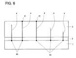
- FIG. 6illustrates a schematic view showing a structure of a conventional group III nitride compound semiconductor.
- a buffer layer 2 and a group III nitride compound semiconductor layer 3are formed successively on a substrate 1 .
- the substrate 1 and the buffer layer 2are made of sapphire and aluminum nitride (AlN), respectively.
- AlN buffer layer 2is formed to relax misfit between the sapphire substrate 1 and the group III nitride compound semiconductor layer 3 , possibility of generating dislocations cannot be 0.
- Feedthrough dislocations 4are propagated from dislocation generating points 40 in longitudinal direction (a direction vertical to a surface of the substrate), penetrating the buffer layer 2 and the group III nitride compound semiconductor layer 3 .
- manufacturing a semiconductor device by laminating various group III nitride compound semiconductor layers on the group III nitride compound semiconductor layer 3results in propagating feedthrough dislocations 4 from dislocation generating points 41 which reach the surface of the group III nitride compound semiconductor layer 3 , further through the semiconductor device in longitudinal direction. Accordingly, it had been difficult to prevent dislocations from propagating in the semiconductor device at the time when a group III nitride compound semiconductor layer is formed.
- an object of the present inventionis to realize an efficient method capable of forming a layer of a group III nitride compound semiconductor without generation of cracks and dislocations to thereby improve device characteristics.
- the present inventionhas a first feature that resides in a method for manufacturing a group III nitride compound semiconductor, which hardly grows epitaxially on a substrate, by crystal growth, comprising: forming a buffer layer on a substrate into an island pattern such as a dot pattern, a striped pattern, or a grid pattern such that substrate-exposed portions are formed in a scattered manner; and forming a group III nitride compound semiconductor layer on the buffer layer by growing a group III nitride compound epitaxially in longitudinal and lateral directions.
- forming substrate-exposed portions in a scattered mannerdoes not necessarily represent the condition that each substrate-exposed portions is completely separated, but represents the condition that the buffer layer exists around arbitrary substrate-exposed portions.
- the following methodcan be applied: forming the buffer layer on the entire surface of the substrate and then removing the desired portions of the buffer layer by etching; or forming a selective mask such as an SiO 2 film on the substrate and partially forming the buffer layer.
- the “lateral” direction as used in the specificationrefers to a direction parallel to a surface of the substrate.
- the group III nitride compound semiconductorgrows on the buffer layer in a longitudinal direction.
- the group III nitride compound semiconductor which grows on the buffer layer in a longitudinal directionalso grows in a lateral direction in order to cover the substrate-exposed portions.
- the growth velocity of the group III nitride compound semiconductor in the longitudinal and lateral directionscan be controlled by conditions of, for example, temperature, pressure, or supplying conditions of source materials.
- a group III nitride compound semiconductor layer reunited into one layercan cover the substrate-exposed portions which are not covered by the buffer layer from a base of the buffer layer which is formed into an island pattern such as a dot pattern, a striped pattern or a grid pattern.
- feedthrough dislocations of the group III nitride compound semiconductorexists only in the regions of group III nitride compound semiconductor layer formed on the buffer layer, which is formed into an island pattern such as a dot pattern, a striped pattern or a grid pattern. This is because feedthrough dislocations are not generated when the group III nitride compound semiconductor grows in a lateral direction but are generated when it grows in a longitudinal direction.
- the second feature of the present inventionis a method for manufacturing a group III nitride compound semiconductor, which hardly grows epitaxially on a substrate, by crystal growth, comprising: forming a buffer layer on a substrate into an island pattern such as a dot pattern, a striped pattern, or a grid pattern such that substrate-exposed portions are formed in a scattered manner; forming a group III nitride compound semiconductor layer on the buffer layer by growing a group III nitride compound epitaxially in longitudinal and lateral directions; etching at least one of the regions of the group III nitride compound semiconductor layer, growing in a longitudinal direction on the buffer layer which is formed into an island pattern; and growing the group III nitride compound semiconductor, which is left without being etched, in a lateral direction. Forming substrate-exposed portions in a scattered manner is explained in the first feature.
- the group III nitride compound semiconductor layeris etched after carrying out the method of the first feature, and then it is grown in a lateral direction in order to cover the etched regions.
- the surface density of longitudinal feedthrough dislocations of the group III nitride compound semiconductor layerdecreases, and crystallinity of the device is thus improved.
- feedthrough dislocations generated by the longitudinal growth of the semiconductor layercan be eliminated. It is preferable to also etch the buffer layer to expose the substrate during etching of the group III nitride compound semiconductor layer.
- the substrate-exposed regionscan be covered and a group III nitride compound semiconductor layer which is reunited into one layer can be obtained.
- the lateral growthcan be promoted by the conditions of, for example, temperature, pressure, or supplying conditions of source materials.
- feedthrough dislocations existing in the group III nitride compound semiconductor layercan be eliminated.
- the group III nitride compound semiconductor layerdoes not have longitudinal feedthrough dislocations, and crystallinity of the device is, therefore, improved.
- the scope of the present inventionalso involves a method of etching regions of the group III nitride compound semiconductor layer, including the upper surface of the buffer layer, wider than the width of the buffer layer in case that feedthrough dislocations are generated partially inclined (in a lateral direction).
- all the regions of the group III nitride compound semiconductor layer which have feedthrough dislocations and grow on the buffer layer, which is formed into an island pattern such as a dot pattern, a striped pattern, or a grid patternis not necessarily etched.
- the group III nitride compound semiconductor layercan be reunited into one layer by growing it in a lateral direction again, even when feedthrough dislocations are left without being etched in the semiconductor layer.
- the scope of the present inventionalso involves a method of dividing etching and epitaxial lateral overgrowth (ELO) components into several parts, according to a position or a design of the regions to form the buffer layer and limitations in the process afterward.
- ELOepitaxial lateral overgrowth
- the third feature of the present inventionis to combine epitaxial growth of a group III nitride compound semiconductor layer formed on the buffer layer in longitudinal direction and epitaxial growth of the group III nitride compound in a lateral direction by using the difference between the velocities of epitaxial growth of the group III nitride compound semiconductor layer on the buffer layer and on the exposed substrate, in order to obtain a group III nitride compound semiconductor layer which covers the surface of the substrate.
- the difference between the velocities of epitaxial growth of the group III nitride compound semiconductor on the buffer layer and on the substratecan be easily controlled by the conditions of, for example, temperature, pressure, or supplying conditions of source materials.
- the velocities of growing the group III nitride compound semiconductor epitaxially on the buffer layer in longitudinal and lateral directionscan be controlled. By controlling these conditions, surface density of feedthrough dislocations of the group III nitride compound semiconductor layer in longitudinal direction is decreased, and crystallinity of the device is improved.
- the difference between the velocities of epitaxial growth of the group III nitride compound semiconductor on the buffer layer and on the substrateis used.
- the group III nitride compound semiconductorcomprises a compound which is identical to that of the buffer layer in view of stoichiometric composition.
- the compound of the group III nitride compound semiconductorcan be non-crystalline, a set of micro-crystalline and polycrystalline, or single-crystalline.
- the difference between the velocities of epitaxial growth of the group III nitride compound semiconductor layer on the buffer layer and on the exposed substrateis an essential point of the present invention, and combination of the group III nitride compound, the compound forming the buffer layer, and materials to form the substrate is a method of generating the different epitaxial growth velocities.
- the fourth feature of the present inventionis that the substrate is made of sapphire. As a result, it is difficult to epitaxially grow the group III nitride compound semiconductor on the substrate.
- the fifth feature of the present inventionis that the buffer layer is made of aluminum nitride (AlN). And the sixth feature of the present invention is that the group III nitride compound semiconductor which grows in lateral direction does not comprise aluminum (Al).
- the seventh feature of the present inventionis to obtain a light-emitting group III nitride compound semiconductor device by forming an another group III nitride compound semiconductor layer on the group III nitride compound semiconductor, which is formed on the region where the buffer layer is not formed, by using the above-described method. Because the group III nitride compound semiconductor layer is laminated on the regions which have no surface density of longitudinal feedthrough dislocations, reliability of the device is improved.
- the eighth feature of the present inventionis to obtain only the group III nitride compound semiconductor layer by using the above-described method.
- the group III nitride compound semiconductor layerwhich is a layer laminated on the substrate, is left by removing the substrate. If necessary, the buffer layer can be removed with the substrate.
- the group III nitride compound semiconductor layercan dope an arbitrary dopant into the substrate so that the substrate has an arbitrary resistivity, and the group III nitride compound semiconductor layer with non-insulated substrate can be obtained. Because the group III nitride compound semiconductor layer has little or no surface density of feedthrough dislocations, it can be useful as a semiconductor substrate.
- FIGS. 1A-1Eare sectional views showing a method for manufacturing the group III nitride compound semiconductor according to a first embodiment of the present invention
- FIG. 2is a sectional view showing a laser diode (LD) using the group III nitride compound semiconductor according to the first embodiment of the present invention
- FIGS. 3A-3Care sectional views showing a method for manufacturing the group III nitride compound semiconductor according to a second embodiment of the present invention.
- FIGS. 4A-4Care views showing the method for manufacturing the group III nitride compound semiconductor according to a second embodiment of the present invention.
- FIG. 5is a view of a buffer layer according to other embodiments of the present invention.
- FIG. 6is a sectional view showing a group III nitride compound semiconductor formed by a conventional method.
- FIGS. 1A-1E, 3 A- 3 C, and 4 A- 4 Ceach show views of processes for manufacturing a group III nitride compound semiconductor according to the first embodiment of the present invention.
- the group III nitride compound semiconductor of the present inventionis formed through the use of a metal organic vapor phase epitaxy (hereinafter referred to as “MOVPE”) method.
- Gases used in the MOVPE methodare ammonia (NH 3 ), carrier gas (H 2 , or N 2 ), trimethyl gallium (Ga(CH 3 ) 3 ) (hereinafter referred to as “TMG”), and trimethyl aluminum (Al(CH 3 ) 3 ) (hereinafter referred to as “TMA”).
- a single crystalline sapphire substrate 1is formed to have a main surface ‘a’ which is cleaned by an organic washing solvent and heat treatment.
- An AlN buffer layer 2having a thickness of about 40 nm, is then formed on the surface ‘a’ of the sapphire substrate 1 under conditions controlled by lowering the temperature to 400° C. and concurrently supplying H 2 , NH 3 and TMA at a flow rate of 10 L/min, 5 L/min, and 20 ⁇ mol/min, respectively, for 3 minutes (FIG. 1 A).
- the buffer layer 2is then dry-etched in a striped pattern by selective dry-etching including reactive ion etching (RIE) using a hard baked resist mask.
- RIEreactive ion etching
- the AlN buffer layer 2is formed in a striped pattern such that each region defined above the buffer layer 2 , has a width of 5 ⁇ m, and each region where the sapphire substrate 1 was exposed, has a width of 5 ⁇ m, and are formed alternately (FIGS. 1 B and 1 E).
- a GaN layer 3 having a thickness of several thousands ⁇was grown to cover the entire surface of the substrate and the AlN buffer layer, while maintaining the substrate 1 at a temperature of 1150° C., and feeding H 2 , NH 3 and TMG at 20 L/min, 10 L/min and 5 ⁇ mol/min, respectively. TMG is then fed at 300 ⁇ mol/min, thereby obtaining about 3 ⁇ m in thickness of GaN layer 3 at a growth temperature of 1000° C.
- the GaN layer 3was formed by growing GaN regions 32 epitaxially on the sapphire substrate 1 in a lateral direction, from the GaN regions 31 which grows epitaxially on the upper surface of the AlN buffer layer 2 in a longitudinal direction and serves as a nucleus (FIGS. 1 C and 1 D). Accordingly, GaN regions 32 having excellent crystallinity can be obtained on the regions where the AlN buffer layer 2 is not formed and the sapphire substrate 1 is exposed.
- a group III nitride compound semiconductor devicecan be formed using the GaN regions 32 having excellent crystallinity, which is formed by epitaxial lateral overgrowth (ELO) method on the upper surface of the sapphire substrate 1 , where predetermined regions of the substrate 1 for forming the device are exposed.
- FIG. 2illustrates a device 100 comprising an LD formed on the GaN regions of high crystallinity in a Si-doped n-type GaN layer 30 .
- the n-GaN regions of high crystallinityis formed in the regions where the AlN buffer layer is not formed, and the following layers are laminated in sequence on each of the regions: an n-Al 0.07 Ga 0.93 N cladding layer 4 c ; an n-GaN guide layer 5 ; an emission layer 6 having a multiple quantum well (MQW) structure, in which a well layer 61 made of Ga 0.9 In 0.1 N and a barrier layer 62 made of Ga 0.97 In 0.03 N were laminated alternately; a p-GaN guide layer 7 ; a p-Al 0.07 Ga 0.93 N cladding layer 8 ; and a p-GaN contact layer 9 .
- MQWmultiple quantum well
- electrodes 11 and 10are formed on the n-GaN layer 30 and the p-GaN contact layer 9 , respectively. Because the LD shown in FIG. 2 does not have feedthrough dislocations except around the electrode 11 , reliability of the LD as a device is improved.
- a single crystalline sapphire substrate 1is formed to have a main surface ‘a’ which is cleaned by an organic washing solvent and heat treatment.
- An AlN buffer layer 2having a thickness of about 40 nm is then formed on the surface ‘a’ of the sapphire substrate 1 under conditions controlled by lowering the temperature to 400° C. and concurrently supplying H 2 , NH 3 and TMA at a flow rate of 10 L/min, 5 L/min, and 20 ⁇ mol/min, respectively, for 3 minutes.
- the buffer layer 2is dry-etched in a striped pattern by selective dry-etching including reactive ion etching (RIE) using a hard baked resist mask.
- RIEreactive ion etching
- the AlN buffer layer 2is formed in a striped pattern such that each region defined above the buffer layer 2 , has a width of 5 ⁇ m, and each region where the sapphire substrate 1 is exposed, has a width of 5 ⁇ m, and are formed alternately.
- a GaN layer 3 having a thickness of several thousands ⁇is grown to cover the entire surface of the substrate and the AlN buffer layer, while maintaining the substrate 1 at a temperature of 1150° C., and feeding H 2 , NH 3 and TMG were fed at 20 L/min, 10 L/min and 5 ⁇ mol/min, respectively. TMG is then fed at 300 ⁇ mol/min, thereby obtaining about 3 ⁇ m in thickness of GaN layer 3 at a growth temperature of 1000° C.
- the GaN layer 3is formed by growing GaN regions 32 epitaxially on the sapphire substrate 1 in a lateral direction, from the GaN regions 31 which grow epitaxially on the upper surface of the AlN buffer layer 2 in a longitudinal direction and serves as a nucleus (FIG. 3 A).
- the GaN regions 31 which grow epitaxially on the upper surface of the AlN buffer layer 2 in a longitudinal directionis dry-etched by selective etching (FIG. 3 B).
- AlN buffer layer 2is also etched.
- a film 3 having a thickness of several thousands ⁇is formed to cover the entire surface of the group III nitride compound semiconductor, while maintaining the substrate 1 at a temperature of 1150° C., and feeding H 2 , NH 3 and TMG at 20 L/min, 10 L/min and 5 ⁇ mol/min, respectively. TMG is then fed at 300 ⁇ mol/min, thereby obtaining about 3 ⁇ m in thickness of GaN layer 3 at a growth temperature of 1000° C.
- GaN region 32 and GaN region 33both have high crystallinity, and are formed on the sapphire substrate 1 .
- the GaN region 32is formed on the sapphire substrate 1 which is exposed by dry-etching the AlN buffer layer 2 .
- the GaN region 33is formed on the sapphire substrate 1 which is exposed by dry-etching the GaN regions 31 and the AlN buffer layer 2 .
- a GaN layer 3which has excellent crystallinity and does not have feedthrough dislocations, can be formed over a wide area W as shown in FIG. 3 C.
- FIGS. 4A-4Care plan views of FIGS. 3A-3C.
- a GaN layer of excellent crystallinityis formed on a region other than a portion where the GaN region 31 , which grows epitaxially on the upper surface of the AlN buffer layer 2 in a longitudinal direction, are formed.
- FIG. 4Aillustrates the buffer layer 2 which is formed in a striped pattern. Regions represented by B are where the sapphire substrate 1 is exposed.
- FIG. 4Bshows the GaN layer 3 left after etching the GaN region 31 and the buffer layer 2 thereunder, which grows epitaxially on the buffer layer 2 in a longitudinal direction. As shown in FIG. 4B, the GaN region 31 which has feedthrough dislocations is left at both sides of the substrate in order to support the GaN regions 32 of higher crystallinity, thus, preventing the GaN region 32 from peeling.
- FIG. 4Cshows the GaN layer 3 reunited into one layer by epitaxial lateral overgrowth (ELO). As shown in FIG. 4C, the GaN layer 3 comprises GaN regions 31 , 32 and 33 .
- ELOepitaxial lateral overgrowth
- the GaN region 31is formed on the buffer layer 2 and has feedthrough dislocations.
- the GaN region 32is formed on the exposed substrate 1 and has no feedthrough dislocations.
- the GaN region 33is formed after removing the buffer layer 2 and the GaN layer 31 and has no feedthrough dislocations. Accordingly, the crystallinity of GaN regions 32 and 33 , or a region W, which has no feedthrough dislocations, is very desirable.
- the sapphire substrate 1 and the buffer layer 2are removed by machinery polishing and then the GaN region 31 which has feedthrough dislocations and is at both side of the substrate is cut.
- the width of the regions defined above the AlN buffer layer 2which are formed in a striped pattern, is 5 ⁇ m, a preferred range for the width is from 1 ⁇ m to 10 ⁇ m. This is because when the width of the regions becomes larger than 10 ⁇ m, the probability of generating dislocations increases. When the width of the regions becomes smaller than 1 ⁇ m, obtaining a GaN layer 3 with wide area and high quality becomes difficult. Additionally, although a width b of the regions B where the substrate 1 is exposed has a width of about 5 ⁇ m, a preferred range for the width is from 1 ⁇ m to 10 ⁇ m.
- the width of the regions Bbecomes larger than 10 ⁇ m, a longer time is required for lateral growth, and when the width of the regions B becomes smaller than 1 ⁇ m, the crystallinity of the GaN region 32 becomes too small.
- the ratio of the width a of the region which is defined above the AlN buffer layer 2 to the width b of the region B where the sapphire substrate 1 is exposed; i.e., a/bpreferably falls within the range of 1 to 10.
- a preferred range for thickness of the n-layer 3 made of GaNis 50 ⁇ m to 100 ⁇ m, because the n-layer 3 can be formed without dislocations.
- the buffer layer 2 and the group III nitride compound semiconductor layer 3comprise aluminum nitride (AlN) and gallium nitride (GaN), respectively. Alternatively, these materials are not limited to AlN and GaN, respectively.
- An essential point of the present inventionis to grow the group III nitride compound semiconductor, which does not grow epitaxially on the substrate, on the buffer layer epitaxially in a longitudinal direction and on the exposed substrate portion in a lateral direction, in order to form regions without feedthrough dislocations.
- the materials of the substrate, the buffer layer, and the composition ratio of the group III nitride compound semiconductorcan be combined in different ways in accordance with different conditions for epitaxial growth.
- sapphireis used to form the substrate 1 .
- silicon (Si), silicon carbide (SiC), and other materialscan be used.
- aluminum nitrideis used to form the buffer layer 2 .
- gallium nitride (GaN), gallium indium nitride (Ga x In 1 ⁇ x N, 0 ⁇ x ⁇ 1), aluminum gallium nitride (Al x Ga 1 ⁇ x N, 0 ⁇ x ⁇ 1) or aluminum gallium indium nitride (Al x Ga y In 1 ⁇ x ⁇ y N, 0 ⁇ x ⁇ 1, 0 ⁇ y ⁇ 1, 0 ⁇ x+y ⁇ 1)may also be used.
- the buffer layer 2is formed in a striped pattern.
- the buffer layer 2can be formed into an island pattern by exposing the substrate 1 in a grid pattern as shown in FIG. 5 .
- the buffer layer 2surrounds the peripheral surface of the substrate in FIG. 5, it is not necessarily present.
- a group III nitride compound semiconductor substratecan be obtained. Except when selectivity of epitaxial growth is prevented, an arbitrary dopant such as silicon (Si), germanium (Ge), zinc (Zn), indium (In), or magnesium (Mg) may be doped into the group III nitride compound semiconductor substrate. Accordingly, the group III nitride compound semiconductor substrate which has an arbitrary resistivity and includes an arbitrary dopant may be obtained.
- a light-emitting diode or a laser devicecomprising various group III nitride compound semiconductors, which is well known to have a double hetero structure comprising a guide layer, a cladding layer, an active layer having an MQW or SQW structure can be formed in the group III nitride compound semiconductor substrate of the present invention.
- a resonator facetcan be easily cleaved because all the layers from the substrate to other layers are made of group III nitride compound semiconductors. As a result, oscillation efficiency of the laser can be improved.
- the group III nitride compound semiconductor substrateto have conductivity, electric current can flow in a vertical direction to the surface of the substrate.
- a process for forming an electrodecan be simplified and the sectional area of the current path becomes wider and the length becomes shorter, resulting in lowering a driving voltage of the device.
- the MOVPE methodis carried out under normal pressure.
- the MOVPE methodcan be carried out under reduced pressure. Further alternatively, it can be carried out under conditions combining normal pressure and reduced pressure.
- the group III nitride compound semiconductor of the present inventioncan be applied not only to a light-emitting device such as an LED or an LD but also to a light-receiving device or an electronic device.
Landscapes
- Engineering & Computer Science (AREA)
- Microelectronics & Electronic Packaging (AREA)
- Physics & Mathematics (AREA)
- Condensed Matter Physics & Semiconductors (AREA)
- General Physics & Mathematics (AREA)
- Manufacturing & Machinery (AREA)
- Computer Hardware Design (AREA)
- Power Engineering (AREA)
- Chemical & Material Sciences (AREA)
- Crystallography & Structural Chemistry (AREA)
- Materials Engineering (AREA)
- Semiconductor Lasers (AREA)
- Led Devices (AREA)
- Crystals, And After-Treatments Of Crystals (AREA)
Abstract
Description
1. Field of the Invention
The present invention relates to a method for manufacturing a group III nitride compound semiconductor. Especially, the present invention relates to a method for manufacturing a group III nitride compound semiconductor in which an epitaxial lateral overgrowth (ELO) method is used to form a layer on a substrate. The present invention also relates to a light-emitting device using a group III nitride compound semiconductor formed on a group III nitride compound semiconductor layer using the ELO method. A group III nitride compound semiconductor can be made of binary compounds such as AlN, GaN or InN, ternary compounds such as AlxGa1−xN, AlxIn1−xN or GaxIn1−x−yN (0<x<1), or quaternary compounds AlxGayIn1−x−yN (0<x<1, 0<y<1, 0<x+y<1), that is, those are represented by a general formula AlxGayIn1−x−yN (0≦x≦1, 0≦y≦1, 0≦x+y≦1).
2. Description of the Related Art
A group III nitride compound semiconductor is a direct-transition-type semiconductor having a wide emission spectrum range from ultraviolet to red, and is applied to light-emitting devices such as light-emitting diodes (LEDs) and laser diodes (LDs). The group III nitride compound semiconductor is, in general, formed on a sapphire substrate.
However, in the above-described conventional technique, when a layer of a group III nitride compound semiconductor is formed on a sapphire substrate, cracks and/or warpage are generated in the semiconductor layer due to a difference in thermal expansion coefficient between sapphire and the group III nitride compound semiconductor, and dislocations are generated in the semiconductor layer due to misfit, which result in degraded device characteristics. Especially, dislocations due to misfit are feedthrough dislocations which penetrate the semiconductor layer in longitudinal direction, resulting in propagation of about 109cm−2of dislocation in the group III nitride compound semiconductor.
FIG. 6 illustrates a schematic view showing a structure of a conventional group III nitride compound semiconductor. In FIG. 6, abuffer layer 2 and a group III nitridecompound semiconductor layer 3 are formed successively on asubstrate 1. In general, thesubstrate 1 and thebuffer layer 2 are made of sapphire and aluminum nitride (AlN), respectively. Although theAlN buffer layer 2 is formed to relax misfit between thesapphire substrate 1 and the group III nitridecompound semiconductor layer 3, possibility of generating dislocations cannot be 0.Feedthrough dislocations 4 are propagated from dislocation generatingpoints 40 in longitudinal direction (a direction vertical to a surface of the substrate), penetrating thebuffer layer 2 and the group III nitridecompound semiconductor layer 3. Thus, manufacturing a semiconductor device by laminating various group III nitride compound semiconductor layers on the group III nitridecompound semiconductor layer 3 results in propagatingfeedthrough dislocations 4 from dislocation generatingpoints 41 which reach the surface of the group III nitridecompound semiconductor layer 3, further through the semiconductor device in longitudinal direction. Accordingly, it had been difficult to prevent dislocations from propagating in the semiconductor device at the time when a group III nitride compound semiconductor layer is formed.
Accordingly, in light of the above problems, an object of the present invention is to realize an efficient method capable of forming a layer of a group III nitride compound semiconductor without generation of cracks and dislocations to thereby improve device characteristics.
In order to solve the above problems, the present invention has a first feature that resides in a method for manufacturing a group III nitride compound semiconductor, which hardly grows epitaxially on a substrate, by crystal growth, comprising: forming a buffer layer on a substrate into an island pattern such as a dot pattern, a striped pattern, or a grid pattern such that substrate-exposed portions are formed in a scattered manner; and forming a group III nitride compound semiconductor layer on the buffer layer by growing a group III nitride compound epitaxially in longitudinal and lateral directions.
Here forming substrate-exposed portions in a scattered manner does not necessarily represent the condition that each substrate-exposed portions is completely separated, but represents the condition that the buffer layer exists around arbitrary substrate-exposed portions. In order to form the buffer layer into an island pattern such as a dot pattern, a striped pattern or a grid pattern, the following method can be applied: forming the buffer layer on the entire surface of the substrate and then removing the desired portions of the buffer layer by etching; or forming a selective mask such as an SiO2film on the substrate and partially forming the buffer layer.
The “lateral” direction as used in the specification refers to a direction parallel to a surface of the substrate. By using the above-described method, the group III nitride compound semiconductor grows on the buffer layer in a longitudinal direction. The group III nitride compound semiconductor which grows on the buffer layer in a longitudinal direction also grows in a lateral direction in order to cover the substrate-exposed portions. The growth velocity of the group III nitride compound semiconductor in the longitudinal and lateral directions can be controlled by conditions of, for example, temperature, pressure, or supplying conditions of source materials. Accordingly, a group III nitride compound semiconductor layer reunited into one layer can cover the substrate-exposed portions which are not covered by the buffer layer from a base of the buffer layer which is formed into an island pattern such as a dot pattern, a striped pattern or a grid pattern. As a result, feedthrough dislocations of the group III nitride compound semiconductor exists only in the regions of group III nitride compound semiconductor layer formed on the buffer layer, which is formed into an island pattern such as a dot pattern, a striped pattern or a grid pattern. This is because feedthrough dislocations are not generated when the group III nitride compound semiconductor grows in a lateral direction but are generated when it grows in a longitudinal direction. Accordingly, surface density of longitudinal feedthrough dislocations of the group III nitride compound semiconductor layer decreases, and crystallinity of the device is improved. When a group III nitride compound semiconductor device which is manufactured using only a group III nitride compound semiconductor layer which is formed on the substrate-exposed portions, or the regions which are not covered by a buffer layer, surface density of feedthrough dislocations of the device can become 0.
The second feature of the present invention is a method for manufacturing a group III nitride compound semiconductor, which hardly grows epitaxially on a substrate, by crystal growth, comprising: forming a buffer layer on a substrate into an island pattern such as a dot pattern, a striped pattern, or a grid pattern such that substrate-exposed portions are formed in a scattered manner; forming a group III nitride compound semiconductor layer on the buffer layer by growing a group III nitride compound epitaxially in longitudinal and lateral directions; etching at least one of the regions of the group III nitride compound semiconductor layer, growing in a longitudinal direction on the buffer layer which is formed into an island pattern; and growing the group III nitride compound semiconductor, which is left without being etched, in a lateral direction. Forming substrate-exposed portions in a scattered manner is explained in the first feature.
In the second feature of the present invention, the group III nitride compound semiconductor layer is etched after carrying out the method of the first feature, and then it is grown in a lateral direction in order to cover the etched regions. As described in the first feature of the present invention, the surface density of longitudinal feedthrough dislocations of the group III nitride compound semiconductor layer decreases, and crystallinity of the device is thus improved. By etching the regions of the group III nitride compound semiconductor layer which grow on the buffer layer in a longitudinal direction and have feedthrough dislocations, feedthrough dislocations generated by the longitudinal growth of the semiconductor layer can be eliminated. It is preferable to also etch the buffer layer to expose the substrate during etching of the group III nitride compound semiconductor layer.
By growing the group III nitride compound semiconductor in a lateral direction again, the substrate-exposed regions can be covered and a group III nitride compound semiconductor layer which is reunited into one layer can be obtained. The lateral growth can be promoted by the conditions of, for example, temperature, pressure, or supplying conditions of source materials. As a result, feedthrough dislocations existing in the group III nitride compound semiconductor layer can be eliminated. Thus, the group III nitride compound semiconductor layer does not have longitudinal feedthrough dislocations, and crystallinity of the device is, therefore, improved. The scope of the present invention also involves a method of etching regions of the group III nitride compound semiconductor layer, including the upper surface of the buffer layer, wider than the width of the buffer layer in case that feedthrough dislocations are generated partially inclined (in a lateral direction). Similarly, all the regions of the group III nitride compound semiconductor layer which have feedthrough dislocations and grow on the buffer layer, which is formed into an island pattern such as a dot pattern, a striped pattern, or a grid pattern, is not necessarily etched. The group III nitride compound semiconductor layer can be reunited into one layer by growing it in a lateral direction again, even when feedthrough dislocations are left without being etched in the semiconductor layer. The scope of the present invention also involves a method of dividing etching and epitaxial lateral overgrowth (ELO) components into several parts, according to a position or a design of the regions to form the buffer layer and limitations in the process afterward.
The third feature of the present invention is to combine epitaxial growth of a group III nitride compound semiconductor layer formed on the buffer layer in longitudinal direction and epitaxial growth of the group III nitride compound in a lateral direction by using the difference between the velocities of epitaxial growth of the group III nitride compound semiconductor layer on the buffer layer and on the exposed substrate, in order to obtain a group III nitride compound semiconductor layer which covers the surface of the substrate. The difference between the velocities of epitaxial growth of the group III nitride compound semiconductor on the buffer layer and on the substrate can be easily controlled by the conditions of, for example, temperature, pressure, or supplying conditions of source materials. Similarly, the velocities of growing the group III nitride compound semiconductor epitaxially on the buffer layer in longitudinal and lateral directions can be controlled. By controlling these conditions, surface density of feedthrough dislocations of the group III nitride compound semiconductor layer in longitudinal direction is decreased, and crystallinity of the device is improved.
In this feature, the difference between the velocities of epitaxial growth of the group III nitride compound semiconductor on the buffer layer and on the substrate is used. But this does not necessarily exclude the possibility that the group III nitride compound semiconductor comprises a compound which is identical to that of the buffer layer in view of stoichiometric composition. Depending on the layer formed under the semiconductor layer and the condition of the epitaxial growth, the compound of the group III nitride compound semiconductor can be non-crystalline, a set of micro-crystalline and polycrystalline, or single-crystalline. The difference between the velocities of epitaxial growth of the group III nitride compound semiconductor layer on the buffer layer and on the exposed substrate is an essential point of the present invention, and combination of the group III nitride compound, the compound forming the buffer layer, and materials to form the substrate is a method of generating the different epitaxial growth velocities.
The fourth feature of the present invention is that the substrate is made of sapphire. As a result, it is difficult to epitaxially grow the group III nitride compound semiconductor on the substrate.
The fifth feature of the present invention is that the buffer layer is made of aluminum nitride (AlN). And the sixth feature of the present invention is that the group III nitride compound semiconductor which grows in lateral direction does not comprise aluminum (Al).
The seventh feature of the present invention is to obtain a light-emitting group III nitride compound semiconductor device by forming an another group III nitride compound semiconductor layer on the group III nitride compound semiconductor, which is formed on the region where the buffer layer is not formed, by using the above-described method. Because the group III nitride compound semiconductor layer is laminated on the regions which have no surface density of longitudinal feedthrough dislocations, reliability of the device is improved.
The eighth feature of the present invention is to obtain only the group III nitride compound semiconductor layer by using the above-described method. The group III nitride compound semiconductor layer, which is a layer laminated on the substrate, is left by removing the substrate. If necessary, the buffer layer can be removed with the substrate. When an insulator is used to form the substrate, the group III nitride compound semiconductor layer can dope an arbitrary dopant into the substrate so that the substrate has an arbitrary resistivity, and the group III nitride compound semiconductor layer with non-insulated substrate can be obtained. Because the group III nitride compound semiconductor layer has little or no surface density of feedthrough dislocations, it can be useful as a semiconductor substrate.
FIGS. 1A-1E are sectional views showing a method for manufacturing the group III nitride compound semiconductor according to a first embodiment of the present invention;
FIG. 2 is a sectional view showing a laser diode (LD) using the group III nitride compound semiconductor according to the first embodiment of the present invention;
FIGS. 3A-3C are sectional views showing a method for manufacturing the group III nitride compound semiconductor according to a second embodiment of the present invention;
FIGS. 4A-4C are views showing the method for manufacturing the group III nitride compound semiconductor according to a second embodiment of the present invention;
FIG. 5 is a view of a buffer layer according to other embodiments of the present invention; and
FIG. 6 is a sectional view showing a group III nitride compound semiconductor formed by a conventional method.
The present invention will now be described by way of concrete embodiments.
FIGS. 1A-1E,3A-3C, and4A-4C each show views of processes for manufacturing a group III nitride compound semiconductor according to the first embodiment of the present invention. The group III nitride compound semiconductor of the present invention is formed through the use of a metal organic vapor phase epitaxy (hereinafter referred to as “MOVPE”) method. Gases used in the MOVPE method are ammonia (NH3), carrier gas (H2, or N2), trimethyl gallium (Ga(CH3)3) (hereinafter referred to as “TMG”), and trimethyl aluminum (Al(CH3)3) (hereinafter referred to as “TMA”).
A singlecrystalline sapphire substrate 1 is formed to have a main surface ‘a’ which is cleaned by an organic washing solvent and heat treatment. AnAlN buffer layer 2, having a thickness of about 40 nm, is then formed on the surface ‘a’ of thesapphire substrate 1 under conditions controlled by lowering the temperature to 400° C. and concurrently supplying H2, NH3and TMA at a flow rate of 10 L/min, 5 L/min, and 20 μmol/min, respectively, for 3 minutes (FIG.1A). Thebuffer layer 2 is then dry-etched in a striped pattern by selective dry-etching including reactive ion etching (RIE) using a hard baked resist mask. Accordingly, theAlN buffer layer 2 is formed in a striped pattern such that each region defined above thebuffer layer 2, has a width of 5 μm, and each region where thesapphire substrate 1 was exposed, has a width of 5 μm, and are formed alternately (FIGS.1B and1E).
AGaN layer 3 having a thickness of several thousands Å was grown to cover the entire surface of the substrate and the AlN buffer layer, while maintaining thesubstrate 1 at a temperature of 1150° C., and feeding H2, NH3and TMG at 20 L/min, 10 L/min and 5 μmol/min, respectively. TMG is then fed at 300 μmol/min, thereby obtaining about 3 μm in thickness ofGaN layer 3 at a growth temperature of 1000° C. In this embodiment, theGaN layer 3 was formed by growingGaN regions 32 epitaxially on thesapphire substrate 1 in a lateral direction, from theGaN regions 31 which grows epitaxially on the upper surface of theAlN buffer layer 2 in a longitudinal direction and serves as a nucleus (FIGS.1C and1D). Accordingly,GaN regions 32 having excellent crystallinity can be obtained on the regions where theAlN buffer layer 2 is not formed and thesapphire substrate 1 is exposed.
A group III nitride compound semiconductor device can be formed using theGaN regions 32 having excellent crystallinity, which is formed by epitaxial lateral overgrowth (ELO) method on the upper surface of thesapphire substrate 1, where predetermined regions of thesubstrate 1 for forming the device are exposed. FIG. 2 illustrates adevice 100 comprising an LD formed on the GaN regions of high crystallinity in a Si-doped n-type GaN layer 30. The n-GaN regions of high crystallinity is formed in the regions where the AlN buffer layer is not formed, and the following layers are laminated in sequence on each of the regions: an n-Al0.07Ga0.93N cladding layer 4c; an n-GaN guide layer 5; anemission layer 6 having a multiple quantum well (MQW) structure, in which awell layer 61 made of Ga0.9In0.1N and a barrier layer62 made of Ga0.97In0.03N were laminated alternately; a p-GaN guide layer 7; a p-Al0.07Ga0.93N cladding layer 8; and a p-GaN contact layer 9. Thenelectrodes GaN layer 30 and the p-GaN contact layer 9, respectively. Because the LD shown in FIG. 2 does not have feedthrough dislocations except around theelectrode 11, reliability of the LD as a device is improved.
A singlecrystalline sapphire substrate 1 is formed to have a main surface ‘a’ which is cleaned by an organic washing solvent and heat treatment. AnAlN buffer layer 2, having a thickness of about 40 nm is then formed on the surface ‘a’ of thesapphire substrate 1 under conditions controlled by lowering the temperature to 400° C. and concurrently supplying H2, NH3and TMA at a flow rate of 10 L/min, 5 L/min, and 20 μmol/min, respectively, for 3 minutes. Thebuffer layer 2 is dry-etched in a striped pattern by selective dry-etching including reactive ion etching (RIE) using a hard baked resist mask. Accordingly, theAlN buffer layer 2 is formed in a striped pattern such that each region defined above thebuffer layer 2, has a width of 5 μm, and each region where thesapphire substrate 1 is exposed, has a width of 5 μm, and are formed alternately.
AGaN layer 3 having a thickness of several thousands Å is grown to cover the entire surface of the substrate and the AlN buffer layer, while maintaining thesubstrate 1 at a temperature of 1150° C., and feeding H2, NH3and TMG were fed at 20 L/min, 10 L/min and 5 μmol/min, respectively. TMG is then fed at 300 μmol/min, thereby obtaining about 3 μm in thickness ofGaN layer 3 at a growth temperature of 1000° C. In this embodiment, theGaN layer 3 is formed by growingGaN regions 32 epitaxially on thesapphire substrate 1 in a lateral direction, from theGaN regions 31 which grow epitaxially on the upper surface of theAlN buffer layer 2 in a longitudinal direction and serves as a nucleus (FIG.3A).
TheGaN regions 31 which grow epitaxially on the upper surface of theAlN buffer layer 2 in a longitudinal direction is dry-etched by selective etching (FIG.3B). In this embodiment,AlN buffer layer 2 is also etched. Afilm 3 having a thickness of several thousands Å is formed to cover the entire surface of the group III nitride compound semiconductor, while maintaining thesubstrate 1 at a temperature of 1150° C., and feeding H2, NH3and TMG at 20 L/min, 10 L/min and 5 μmol/min, respectively. TMG is then fed at 300 μmol/min, thereby obtaining about 3 μm in thickness ofGaN layer 3 at a growth temperature of 1000° C. TMG is then fed to the device at 300 μmol/min, wherein each space where theGaN region 31 is removed is covered again by growing aregion 33 in a lateral direction at a growth temperature of 1000° C., and theGaN layer 3 is obtained having a thickness about 3 μm (FIG.3C). Accordingly,GaN region 32 andGaN region 33, both have high crystallinity, and are formed on thesapphire substrate 1. TheGaN region 32 is formed on thesapphire substrate 1 which is exposed by dry-etching theAlN buffer layer 2. TheGaN region 33 is formed on thesapphire substrate 1 which is exposed by dry-etching theGaN regions 31 and theAlN buffer layer 2. As a result, aGaN layer 3, which has excellent crystallinity and does not have feedthrough dislocations, can be formed over a wide area W as shown in FIG.3C.
FIGS. 4A-4C are plan views of FIGS. 3A-3C. In this embodiment, a GaN layer of excellent crystallinity is formed on a region other than a portion where theGaN region 31, which grows epitaxially on the upper surface of theAlN buffer layer 2 in a longitudinal direction, are formed.
FIG. 4A illustrates thebuffer layer 2 which is formed in a striped pattern. Regions represented by B are where thesapphire substrate 1 is exposed. FIG. 4B shows theGaN layer 3 left after etching theGaN region 31 and thebuffer layer 2 thereunder, which grows epitaxially on thebuffer layer 2 in a longitudinal direction. As shown in FIG. 4B, theGaN region 31 which has feedthrough dislocations is left at both sides of the substrate in order to support theGaN regions 32 of higher crystallinity, thus, preventing theGaN region 32 from peeling. FIG. 4C shows theGaN layer 3 reunited into one layer by epitaxial lateral overgrowth (ELO). As shown in FIG. 4C, theGaN layer 3 comprisesGaN regions GaN region 31 is formed on thebuffer layer 2 and has feedthrough dislocations. TheGaN region 32 is formed on the exposedsubstrate 1 and has no feedthrough dislocations. TheGaN region 33 is formed after removing thebuffer layer 2 and theGaN layer 31 and has no feedthrough dislocations. Accordingly, the crystallinity ofGaN regions
After the above-described process, thesapphire substrate 1 and thebuffer layer 2 are removed by machinery polishing and then theGaN region 31 which has feedthrough dislocations and is at both side of the substrate is cut. As a result, a group III nitride compound semiconductor substrate of excellent crystallinity, comprising theGaN layer 3 which has no feedthrough dislocations, is obtained.
Although the width of the regions defined above theAlN buffer layer 2, which are formed in a striped pattern, is 5 μm, a preferred range for the width is from 1 μm to 10 μm. This is because when the width of the regions becomes larger than 10 μm, the probability of generating dislocations increases. When the width of the regions becomes smaller than 1 μm, obtaining aGaN layer 3 with wide area and high quality becomes difficult. Additionally, although a width b of the regions B where thesubstrate 1 is exposed has a width of about 5 μm, a preferred range for the width is from 1 μm to 10 μm. This is because when the width of the regions B becomes larger than 10 μm, a longer time is required for lateral growth, and when the width of the regions B becomes smaller than 1 μm, the crystallinity of theGaN region 32 becomes too small. Further, in view of the crystallinity of the n-layer 3 made of GaN, the ratio of the width a of the region which is defined above theAlN buffer layer 2 to the width b of the region B where thesapphire substrate 1 is exposed; i.e., a/b, preferably falls within the range of 1 to 10.
In the above embodiments, a preferred range for thickness of the n-layer 3 made of GaN is 50 μm to 100 μm, because the n-layer 3 can be formed without dislocations.
In the present embodiment, thebuffer layer 2 and the group III nitridecompound semiconductor layer 3 comprise aluminum nitride (AlN) and gallium nitride (GaN), respectively. Alternatively, these materials are not limited to AlN and GaN, respectively. An essential point of the present invention is to grow the group III nitride compound semiconductor, which does not grow epitaxially on the substrate, on the buffer layer epitaxially in a longitudinal direction and on the exposed substrate portion in a lateral direction, in order to form regions without feedthrough dislocations. The materials of the substrate, the buffer layer, and the composition ratio of the group III nitride compound semiconductor can be combined in different ways in accordance with different conditions for epitaxial growth. Accordingly, when sapphire and aluminum nitride (AlN) are used to form the substrate and the buffer layer, respectively, a group III nitride compound semiconductor represented by a general formula AlxGayIn1−x−yN (0≦x≦1, 0≦y≦1, 0≦x+y≦1, except AlN, when x=1 and y=0) and having an arbitrary composition ratio may be used to form the group III nitride compound semiconductor.
In the above embodiments, sapphire is used to form thesubstrate 1. Alternatively, silicon (Si), silicon carbide (SiC), and other materials can be used.
In the embodiments, aluminum nitride (AlN) is used to form thebuffer layer 2. Alternatively, gallium nitride (GaN), gallium indium nitride (GaxIn1−xN, 0<x<1), aluminum gallium nitride (AlxGa1−xN, 0<x<1) or aluminum gallium indium nitride (AlxGayIn1−x−yN, 0<x<1, 0<y<1, 0<x+y<1) may also be used.
In the embodiments, thebuffer layer 2 is formed in a striped pattern. Alternatively, thebuffer layer 2 can be formed into an island pattern by exposing thesubstrate 1 in a grid pattern as shown in FIG.5. Although thebuffer layer 2 surrounds the peripheral surface of the substrate in FIG. 5, it is not necessarily present.
As described above, a group III nitride compound semiconductor substrate can be obtained. Except when selectivity of epitaxial growth is prevented, an arbitrary dopant such as silicon (Si), germanium (Ge), zinc (Zn), indium (In), or magnesium (Mg) may be doped into the group III nitride compound semiconductor substrate. Accordingly, the group III nitride compound semiconductor substrate which has an arbitrary resistivity and includes an arbitrary dopant may be obtained.
A light-emitting diode or a laser device comprising various group III nitride compound semiconductors, which is well known to have a double hetero structure comprising a guide layer, a cladding layer, an active layer having an MQW or SQW structure can be formed in the group III nitride compound semiconductor substrate of the present invention. For example, when a laser diode is formed on the group III nitride compound semiconductor substrate, a resonator facet can be easily cleaved because all the layers from the substrate to other layers are made of group III nitride compound semiconductors. As a result, oscillation efficiency of the laser can be improved. And by forming the group III nitride compound semiconductor substrate to have conductivity, electric current can flow in a vertical direction to the surface of the substrate. As a result, a process for forming an electrode can be simplified and the sectional area of the current path becomes wider and the length becomes shorter, resulting in lowering a driving voltage of the device.
In the above embodiments, the MOVPE method is carried out under normal pressure. Alternatively, the MOVPE method can be carried out under reduced pressure. Further alternatively, it can be carried out under conditions combining normal pressure and reduced pressure. The group III nitride compound semiconductor of the present invention can be applied not only to a light-emitting device such as an LED or an LD but also to a light-receiving device or an electronic device.
While the invention has been described in connection with what are presently considered to be the most practical and preferred embodiments, it is to be understood that the invention is not to be limited to the disclosed embodiments, but on the contrary, is intended to cover various modifications and equivalent arrangements included within the spirit and scope of the appended claims.
Claims (9)
1. A method for manufacturing a group III nitride compound semiconductor, which hardly grows epitaxially on a substrate by crystal growth, comprising:
forming a buffer layer on said substrate into an island pattern such as a dot pattern, a striped pattern, or a grid pattern such that substrate-exposed portions are formed in a scattered manner; and
forming a group III nitride compound semiconductor layer on said island patterned buffer layer by growing said group III nitride compound epitaxially in longitudinal and lateral directions; wherein a width of said substrate-exposed portions fall within the range of 1 to 10 multiplied by a width of said island patterned buffer layer.
2. A method for manufacturing a group III nitride compound semiconductor according toclaim 1 , further comprising:
combining epitaxial growth of said group III nitride compound formed on said island patterned buffer layer in a longitudinal direction and epitaxial growth of said group III nitride compound in a lateral direction by using the difference between the velocities of epitaxial growth of said group III nitride compound semiconductor layer on said buffer layer and on said substrate, in order to obtain a group III nitride compound semiconductor layer which covers the surface of said substrate.
3. A method for manufacturing a group III nitride compound semiconductor according toclaim 1 , wherein said substrate is made of sapphire.
4. A method for manufacturing a group III nitride compound semiconductor according toclaim 1 , wherein said buffer layer is made of aluminum nitride (AlN).
5. A method for manufacturing a group III nitride compound semiconductor according toclaim 1 , wherein said group III nitride compound semiconductor growing in a lateral direction does not comprise aluminum (Al).
6. A method for manufacturing a group III nitride compound semiconductor according toclaim 1 , further comprising:
forming an another group III nitride compound semiconductor layer on said group III nitride compound semiconductor in order to obtain a light-emitting group III nitride compound semiconductor device, wherein said group III nitride compound semiconductor is formed on a region where said island patterned buffer layer is not formed.
7. A method for manufacturing a group III nitride compound semiconductor according toclaim 1 , further comprising:
removing said substrate in order to obtain only said group III nitride compound semiconductor layer.
8. A light-emitting group III nitride compound semiconductor device formed by the method ofclaim 6 .
9. A group III nitride compound semiconductor substrate formed by the method ofclaim 7 .
Priority Applications (1)
| Application Number | Priority Date | Filing Date | Title |
|---|---|---|---|
| US10/187,943US6790279B2 (en) | 1999-05-10 | 2002-07-02 | Method for manufacturing group III nitride compound semiconductor and a light-emitting device using group III nitride compound semiconductor |
Applications Claiming Priority (2)
| Application Number | Priority Date | Filing Date | Title |
|---|---|---|---|
| JP12932299AJP3587081B2 (en) | 1999-05-10 | 1999-05-10 | Method of manufacturing group III nitride semiconductor and group III nitride semiconductor light emitting device |
| JP11-129322 | 1999-05-10 |
Related Child Applications (1)
| Application Number | Title | Priority Date | Filing Date |
|---|---|---|---|
| US10/187,943DivisionUS6790279B2 (en) | 1999-05-10 | 2002-07-02 | Method for manufacturing group III nitride compound semiconductor and a light-emitting device using group III nitride compound semiconductor |
Publications (1)
| Publication Number | Publication Date |
|---|---|
| US6645295B1true US6645295B1 (en) | 2003-11-11 |
Family
ID=15006728
Family Applications (2)
| Application Number | Title | Priority Date | Filing Date |
|---|---|---|---|
| US09/566,917Expired - LifetimeUS6645295B1 (en) | 1999-05-10 | 2000-05-09 | Method for manufacturing group III nitride compound semiconductor and a light-emitting device using group III nitride compound semiconductor |
| US10/187,943Expired - LifetimeUS6790279B2 (en) | 1999-05-10 | 2002-07-02 | Method for manufacturing group III nitride compound semiconductor and a light-emitting device using group III nitride compound semiconductor |
Family Applications After (1)
| Application Number | Title | Priority Date | Filing Date |
|---|---|---|---|
| US10/187,943Expired - LifetimeUS6790279B2 (en) | 1999-05-10 | 2002-07-02 | Method for manufacturing group III nitride compound semiconductor and a light-emitting device using group III nitride compound semiconductor |
Country Status (3)
| Country | Link |
|---|---|
| US (2) | US6645295B1 (en) |
| EP (1) | EP1052684A1 (en) |
| JP (1) | JP3587081B2 (en) |
Cited By (39)
| Publication number | Priority date | Publication date | Assignee | Title |
|---|---|---|---|---|
| US20030198837A1 (en)* | 2002-04-15 | 2003-10-23 | Craven Michael D. | Non-polar a-plane gallium nitride thin films grown by metalorganic chemical vapor deposition |
| WO2004061909A1 (en)* | 2002-12-16 | 2004-07-22 | The Regents Of The University Of California | Growth of reduced dislocation density non-polar gallium nitride by hydride vapor phase epitaxy |
| US20050214992A1 (en)* | 2002-12-16 | 2005-09-29 | The Regents Of The University Of California | Fabrication of nonpolar indium gallium nitride thin films, heterostructures and devices by metalorganic chemical vapor deposition |
| US20050245095A1 (en)* | 2002-04-15 | 2005-11-03 | The Regents Of The University Of California | Growth of planar reduced dislocation density m-plane gallium nitride by hydride vapor phase epitaxy |
| US20060008941A1 (en)* | 2002-12-16 | 2006-01-12 | Basf Aktiengesellschaft | Growth of planar, non-polar a-plane gallium nitride by hydride vapor phase epitaxy |
| US20060270076A1 (en)* | 2005-05-31 | 2006-11-30 | The Regents Of The University Of California | Defect reduction of non-polar and semi-polar III-nitrides with sidewall lateral epitaxial overgrowth (SLEO) |
| US20060276043A1 (en)* | 2003-03-21 | 2006-12-07 | Johnson Mark A L | Method and systems for single- or multi-period edge definition lithography |
| US20070111488A1 (en)* | 2004-05-10 | 2007-05-17 | The Regents Of The University Of California | Fabrication of nonpolar indium gallium nitride thin films, heterostructures and devices by metalorganic chemical vapor deposition |
| US20070184637A1 (en)* | 2004-06-03 | 2007-08-09 | The Regents Of The University Of California | Growth of planar reduced dislocation density m-plane gallium nitride by hydride vapor phase epitaxy |
| US20070295971A1 (en)* | 2006-06-13 | 2007-12-27 | Hee Jin Kim | Light Emitting Device and Method for Fabricating the Same |
| US20080113496A1 (en)* | 2006-11-15 | 2008-05-15 | The Regents Of The University Of California | METHOD FOR HETEROEPITAXIAL GROWTH OF HIGH-QUALITY N-FACE GaN, InN, AND AlN AND THEIR ALLOYS BY METAL ORGANIC CHEMICAL VAPOR DEPOSITION |
| US20080135853A1 (en)* | 2002-04-15 | 2008-06-12 | The Regents Of The University Of California | Dislocation reduction in non-polar iii-nitride thin films |
| US20080163814A1 (en)* | 2006-12-12 | 2008-07-10 | The Regents Of The University Of California | CRYSTAL GROWTH OF M-PLANE AND SEMIPOLAR PLANES OF (Al, In, Ga, B)N ON VARIOUS SUBSTRATES |
| US20090246944A1 (en)* | 2006-11-15 | 2009-10-01 | The Regents Of The University Of California | METHOD FOR HETEROEPITAXIAL GROWTH OF HIGH-QUALITY N-FACE GaN, InN, AND AlN AND THEIR ALLOYS BY METAL ORGANIC CHEMICAL VAPOR DEPOSITION |
| US20120043578A1 (en)* | 2010-08-23 | 2012-02-23 | Su-Hui Lin | GaN-Based Light-Emitting Diode and Method for Manufacturing the Same |
| US20120112320A1 (en)* | 2009-06-01 | 2012-05-10 | Mitsubishi Chemical Corporation | Nitride semiconductor crystal and production process thereof |
| US8216951B2 (en) | 2006-09-27 | 2012-07-10 | Taiwan Semiconductor Manufacturing Company, Ltd. | Quantum tunneling devices and circuits with lattice-mismatched semiconductor structures |
| US8237151B2 (en) | 2009-01-09 | 2012-08-07 | Taiwan Semiconductor Manufacturing Company, Ltd. | Diode-based devices and methods for making the same |
| US8253211B2 (en) | 2008-09-24 | 2012-08-28 | Taiwan Semiconductor Manufacturing Company, Ltd. | Semiconductor sensor structures with reduced dislocation defect densities |
| US8274097B2 (en) | 2008-07-01 | 2012-09-25 | Taiwan Semiconductor Manufacturing Company, Ltd. | Reduction of edge effects from aspect ratio trapping |
| US8304805B2 (en) | 2009-01-09 | 2012-11-06 | Taiwan Semiconductor Manufacturing Company, Ltd. | Semiconductor diodes fabricated by aspect ratio trapping with coalesced films |
| US8324660B2 (en) | 2005-05-17 | 2012-12-04 | Taiwan Semiconductor Manufacturing Company, Ltd. | Lattice-mismatched semiconductor structures with reduced dislocation defect densities and related methods for device fabrication |
| US8329541B2 (en) | 2007-06-15 | 2012-12-11 | Taiwan Semiconductor Manufacturing Company, Ltd. | InP-based transistor fabrication |
| US8344242B2 (en) | 2007-09-07 | 2013-01-01 | Taiwan Semiconductor Manufacturing Company, Ltd. | Multi-junction solar cells |
| US8384196B2 (en) | 2008-09-19 | 2013-02-26 | Taiwan Semiconductor Manufacturing Company, Ltd. | Formation of devices by epitaxial layer overgrowth |
| US8502263B2 (en) | 2006-10-19 | 2013-08-06 | Taiwan Semiconductor Manufacturing Company, Ltd. | Light-emitter-based devices with lattice-mismatched semiconductor structures |
| US8624103B2 (en) | 2007-04-09 | 2014-01-07 | Taiwan Semiconductor Manufacturing Company, Ltd. | Nitride-based multi-junction solar cell modules and methods for making the same |
| US8629446B2 (en) | 2009-04-02 | 2014-01-14 | Taiwan Semiconductor Manufacturing Company, Ltd. | Devices formed from a non-polar plane of a crystalline material and method of making the same |
| US8822248B2 (en) | 2008-06-03 | 2014-09-02 | Taiwan Semiconductor Manufacturing Company, Ltd. | Epitaxial growth of crystalline material |
| US8847279B2 (en) | 2006-09-07 | 2014-09-30 | Taiwan Semiconductor Manufacturing Company, Ltd. | Defect reduction using aspect ratio trapping |
| US8878243B2 (en) | 2006-03-24 | 2014-11-04 | Taiwan Semiconductor Manufacturing Company, Ltd. | Lattice-mismatched semiconductor structures and related methods for device fabrication |
| US8981427B2 (en) | 2008-07-15 | 2015-03-17 | Taiwan Semiconductor Manufacturing Company, Ltd. | Polishing of small composite semiconductor materials |
| US9048385B2 (en) | 2009-06-24 | 2015-06-02 | Nichia Corporation | Nitride semiconductor light emitting diode |
| US9508890B2 (en) | 2007-04-09 | 2016-11-29 | Taiwan Semiconductor Manufacturing Company, Ltd. | Photovoltaics on silicon |
| US9859381B2 (en) | 2005-05-17 | 2018-01-02 | Taiwan Semiconductor Manufacturing Company, Ltd. | Lattice-mismatched semiconductor structures with reduced dislocation defect densities and related methods for device fabrication |
| US9984872B2 (en) | 2008-09-19 | 2018-05-29 | Taiwan Semiconductor Manufacturing Company, Ltd. | Fabrication and structures of crystalline material |
| US11056338B2 (en) | 2018-10-10 | 2021-07-06 | The Johns Hopkins University | Method for printing wide bandgap semiconductor materials |
| US20220285500A1 (en)* | 2021-03-05 | 2022-09-08 | United Microelectronics Corp. | Semiconductor Device and Fabricating Method Thereof |
| US11823900B2 (en) | 2018-10-10 | 2023-11-21 | The Johns Hopkins University | Method for printing wide bandgap semiconductor materials |
Families Citing this family (35)
| Publication number | Priority date | Publication date | Assignee | Title |
|---|---|---|---|---|
| WO2002064864A1 (en) | 2001-02-14 | 2002-08-22 | Toyoda Gosei Co., Ltd. | Production method for semiconductor crystal and semiconductor luminous element |
| US6673646B2 (en)* | 2001-02-28 | 2004-01-06 | Motorola, Inc. | Growth of compound semiconductor structures on patterned oxide films and process for fabricating same |
| CN1284250C (en)* | 2001-03-21 | 2006-11-08 | 三菱电线工业株式会社 | Semiconductor light emitting element |
| JP3705142B2 (en)* | 2001-03-27 | 2005-10-12 | ソニー株式会社 | Nitride semiconductor device and manufacturing method thereof |
| EP1245701A3 (en)* | 2001-03-28 | 2009-03-04 | Ngk Insulators, Ltd. | A method of fabricating a Group III nitride film |
| JP4817522B2 (en)* | 2001-04-06 | 2011-11-16 | 三洋電機株式会社 | Nitride-based semiconductor layer device and method for forming nitride-based semiconductor |
| JP3956637B2 (en)* | 2001-04-12 | 2007-08-08 | ソニー株式会社 | Nitride semiconductor crystal growth method and semiconductor element formation method |
| JP2003007999A (en)* | 2001-06-26 | 2003-01-10 | Sony Corp | Iii-v nitride-based compound semiconductor substrate, its manufacturing method, method of manufacturing semiconductor light emitting element, and method of manufacturing semiconductor device |
| JP3864870B2 (en)* | 2001-09-19 | 2007-01-10 | 住友電気工業株式会社 | Single crystal gallium nitride substrate, growth method thereof, and manufacturing method thereof |
| JP4092927B2 (en)* | 2002-02-28 | 2008-05-28 | 豊田合成株式会社 | Group III nitride compound semiconductor, group III nitride compound semiconductor element, and method for manufacturing group III nitride compound semiconductor substrate |
| GB0220438D0 (en)* | 2002-09-03 | 2002-10-09 | Univ Warwick | Formation of lattice-turning semiconductor substrates |
| JP2004107114A (en)* | 2002-09-17 | 2004-04-08 | Toyoda Gosei Co Ltd | Method of manufacturing group iii nitride compound semiconductor substrate |
| US7872268B2 (en) | 2004-04-22 | 2011-01-18 | Cree, Inc. | Substrate buffer structure for group III nitride devices |
| KR100638609B1 (en) | 2004-08-04 | 2006-10-26 | 삼성전기주식회사 | Nitride semiconductor crystal growth method and nitride semiconductor device manufacturing method |
| KR100918967B1 (en) | 2004-12-29 | 2009-09-25 | 갤럭시아포토닉스 주식회사 | Gallium nitride device having light scattering means in buffer layer and fabrication method thereof |
| JP5024722B2 (en)* | 2005-06-06 | 2012-09-12 | 住友電気工業株式会社 | Nitride semiconductor substrate and manufacturing method thereof |
| TWI385820B (en)* | 2007-08-24 | 2013-02-11 | Sino American Silicon Prod Inc | Semiconductor light emitting element and method of manufacturing same |
| TWI344225B (en)* | 2007-10-05 | 2011-06-21 | Sino American Silicon Prod Inc | Semiconductor light-emitting device and method of fabricating the same |
| JP5085369B2 (en) | 2008-02-18 | 2012-11-28 | 日本オクラロ株式会社 | Nitride semiconductor light emitting device and manufacturing method thereof |
| US8779445B2 (en)* | 2008-07-02 | 2014-07-15 | Taiwan Semiconductor Manufacturing Company, Ltd. | Stress-alleviation layer for LED structures |
| JP2010040867A (en) | 2008-08-06 | 2010-02-18 | Showa Denko Kk | Group iii nitride semiconductor laminated structure and method of manufacturing same |
| CN102239538A (en) | 2008-09-24 | 2011-11-09 | S.O.I.探测硅绝缘技术公司 | Methods of forming layers of relaxed semiconductor material, semiconductor structures, devices and engineered substrates comprising layers of relaxed semiconductor material, semiconductor structures, devices |
| WO2010056443A1 (en) | 2008-10-30 | 2010-05-20 | S.O.I.Tec Silicon On Insulator Technologies | Methods of forming layers of semiconductor material having reduced lattice strain, semiconductor structures, devices and engineered substrates including same |
| US8637383B2 (en) | 2010-12-23 | 2014-01-28 | Soitec | Strain relaxation using metal materials and related structures |
| CN101877377B (en) | 2009-04-30 | 2011-12-14 | 比亚迪股份有限公司 | Epitaxial wafer of discrete light-emitting diode and manufacturing method thereof |
| US9029866B2 (en) | 2009-08-04 | 2015-05-12 | Gan Systems Inc. | Gallium nitride power devices using island topography |
| US9818857B2 (en) | 2009-08-04 | 2017-11-14 | Gan Systems Inc. | Fault tolerant design for large area nitride semiconductor devices |
| AU2010281317A1 (en) | 2009-08-04 | 2012-02-23 | Gan Systems Inc. | Island matrixed gallium nitride microwave and power switching transistors |
| EP2559064A4 (en)* | 2010-04-13 | 2018-07-18 | GaN Systems Inc. | High density gallium nitride devices using island topology |
| JP5117596B2 (en) | 2011-05-16 | 2013-01-16 | 株式会社東芝 | Semiconductor light emitting device, wafer, and method of manufacturing nitride semiconductor crystal layer |
| DE102011077542B4 (en) | 2011-06-15 | 2020-06-18 | Osram Opto Semiconductors Gmbh | OPTOELECTRONIC SEMICONDUCTOR BODY AND METHOD FOR PRODUCING AN OPTOELECTRONIC SEMICONDUCTOR BODY |
| JP2015521365A (en)* | 2012-04-13 | 2015-07-27 | タンデム スン アーベー | Manufacturing method of semiconductor method device based on epitaxial growth |
| CN104716241B (en)* | 2015-03-16 | 2018-10-16 | 映瑞光电科技(上海)有限公司 | A kind of LED structure and preparation method thereof |
| JP6679022B2 (en)* | 2016-02-29 | 2020-04-15 | 信越化学工業株式会社 | Diamond substrate manufacturing method |
| WO2025115743A1 (en)* | 2023-11-30 | 2025-06-05 | 京セラ株式会社 | Semiconductor substrate, production method and production apparatus for same, and semiconductor device |
Citations (72)
| Publication number | Priority date | Publication date | Assignee | Title |
|---|---|---|---|---|
| JPS4895181A (en) | 1972-03-15 | 1973-12-06 | ||
| JPS51137393A (en) | 1975-05-22 | 1976-11-27 | Mitsubishi Electric Corp | Manufacturing method for semiconductor light emitting device |
| JPS5534646A (en) | 1978-08-30 | 1980-03-11 | Sumitomo Metal Ind Ltd | Heating method for furnace body in blowing-in of shaft furnace |
| JPS57115849A (en) | 1981-01-12 | 1982-07-19 | Fujitsu Ltd | Manufacture of substrate for semiconductor device |
| JPS5833882A (en) | 1981-08-21 | 1983-02-28 | Mitsubishi Electric Corp | Manufacture of light emitting diode |
| JPH01316459A (en) | 1988-06-15 | 1989-12-21 | Murata Mfg Co Ltd | In-line sputtering device and method |
| JPH03133182A (en) | 1989-10-19 | 1991-06-06 | Showa Denko Kk | Semiconductor substrate and manufacture thereof |
| JPH0410665A (en) | 1990-04-27 | 1992-01-14 | Toyoda Gosei Co Ltd | Light-emitting element of gallium nitride-based compound semiconductor |
| JPH0484418A (en) | 1990-07-27 | 1992-03-17 | Nec Corp | Method of heteroepitaxial development of iii-v group compound semiconductor for different types of substrates |
| US5185290A (en) | 1989-08-17 | 1993-02-09 | Mitsubishi Denki Kabushiki Kaisha | Method of coating facet of semiconductor optical element |
| JPH0541536A (en) | 1991-05-30 | 1993-02-19 | Kyocera Corp | Manufacture of semiconductor light emitting device |
| JPH05110206A (en) | 1991-10-16 | 1993-04-30 | Kubota Corp | Method and apparatus for producing light emitting semiconductor element |
| EP0551721A2 (en) | 1991-12-18 | 1993-07-21 | Amano, Hiroshi | Gallium nitride base semiconductor device and method of fabricating the same |
| JPH06196757A (en) | 1992-06-10 | 1994-07-15 | Nichia Chem Ind Ltd | Method of growing indium gallium nitride semiconductor |
| JPH07249830A (en) | 1994-03-10 | 1995-09-26 | Hitachi Ltd | Method for manufacturing semiconductor light emitting device |
| JPH07273367A (en) | 1994-04-01 | 1995-10-20 | Mitsubishi Cable Ind Ltd | Manufacture of semiconductor substrate and light-emitting device |
| JPH0864791A (en) | 1994-08-23 | 1996-03-08 | Matsushita Electric Ind Co Ltd | Epitaxial growth method |
| JPH08102549A (en) | 1994-09-30 | 1996-04-16 | Rohm Co Ltd | Semiconductor light emitting element |
| JPH08222812A (en) | 1995-02-17 | 1996-08-30 | Matsushita Electric Ind Co Ltd | Crystal growth method for gallium nitride-based compound semiconductor |
| WO1997011518A1 (en) | 1995-09-18 | 1997-03-27 | Hitachi, Ltd. | Semiconductor material, method of producing the semiconductor material, and semiconductor device |
| EP0779666A2 (en) | 1995-12-11 | 1997-06-18 | Mitsubishi Denki Kabushiki Kaisha | Semiconductor device and method of fabricating semiconductor device |
| US5798536A (en) | 1996-01-25 | 1998-08-25 | Rohm Co., Ltd. | Light-emitting semiconductor device and method for manufacturing the same |
| WO1998047170A1 (en) | 1997-04-11 | 1998-10-22 | Nichia Chemical Industries, Ltd. | Method of growing nitride semiconductors, nitride semiconductor substrate and nitride semiconductor device |
| JPH10312971A (en) | 1997-03-13 | 1998-11-24 | Nec Corp | III-V compound semiconductor film and its growth method, GaN-based semiconductor film and its formation method, GaN-based semiconductor laminated structure and its formation method, GaN-based semiconductor element and its production method |
| JPH10321954A (en) | 1997-05-15 | 1998-12-04 | Fuji Electric Co Ltd | Group III nitride semiconductor device and method of manufacturing the same |
| WO1999001594A1 (en) | 1997-07-03 | 1999-01-14 | Cbl Technologies | Thermal mismatch compensation to produce free standing substrates by epitaxial deposition |
| JPH1131864A (en) | 1997-07-11 | 1999-02-02 | Nec Corp | Crystal growth of low-migration gallium nitride |
| JPH11145519A (en) | 1997-09-02 | 1999-05-28 | Toshiba Corp | Semiconductor light emitting element, semiconductor light emitting device, and image display device |
| JPH11145516A (en) | 1997-11-07 | 1999-05-28 | Toyoda Gosei Co Ltd | Manufacture of gallium nitride compound semiconductor |
| JPH11191657A (en) | 1997-04-11 | 1999-07-13 | Nichia Chem Ind Ltd | Method for growing nitride semiconductor and nitride semiconductor device |
| JPH11191533A (en) | 1997-05-16 | 1999-07-13 | Nichia Chem Ind Ltd | Method for growing nitride semiconductor |
| JPH11191659A (en) | 1997-10-09 | 1999-07-13 | Nichia Chem Ind Ltd | Method for growing nitride semiconductor and nitride semiconductor device |
| JPH11219910A (en) | 1997-11-26 | 1999-08-10 | Nichia Chem Ind Ltd | Method for growing nitride semiconductor and nitride semiconductor device |
| JPH11251632A (en) | 1998-02-27 | 1999-09-17 | Toyoda Gosei Co Ltd | Manufacture of gallium nitride semiconductor element |
| JPH11260737A (en) | 1998-03-09 | 1999-09-24 | Ricoh Co Ltd | Manufacture of semiconductor substrate and semiconductor light emitting element |
| EP0951055A2 (en) | 1998-04-17 | 1999-10-20 | Hewlett-Packard Company | Epitaxial material grown laterally within a trench |
| JPH11312825A (en) | 1998-04-28 | 1999-11-09 | Nichia Chem Ind Ltd | Method for growing nitride semiconductor and nitride semiconductor device |
| JPH11330546A (en) | 1998-05-12 | 1999-11-30 | Fuji Electric Co Ltd | Group III nitride semiconductor and method of manufacturing the same |
| JPH11329971A (en) | 1998-05-18 | 1999-11-30 | Sharp Corp | Crystal substrate and method of manufacturing GaN-based crystal film |
| JPH11340508A (en) | 1998-05-28 | 1999-12-10 | Nichia Chem Ind Ltd | Method for growing nitride semiconductor and nitride semiconductor device |
| JP2000021789A (en) | 1997-08-29 | 2000-01-21 | Toshiba Corp | Nitride-based semiconductor device, light-emitting device and method of manufacturing the same |
| JP2000044121A (en) | 1998-08-03 | 2000-02-15 | Murata Mach Ltd | Sliver guide creel for spinning machine |
| JP2000091253A (en) | 1999-10-12 | 2000-03-31 | Toyoda Gosei Co Ltd | Method of producing gallium nitride based compound semiconductor |
| JP2000106473A (en) | 1998-07-29 | 2000-04-11 | Sanyo Electric Co Ltd | Semiconductor device, semiconductor light emitting device and manufacture thereof, and forming method of nitride semiconductor layer |
| JP2000106455A (en) | 1998-07-31 | 2000-04-11 | Sharp Corp | Nitride semiconductor structure, its manufacturing method and light emitting device |
| EP0993048A2 (en) | 1998-09-14 | 2000-04-12 | Matsushita Electronics Corporation | Nitride semiconductor device and its manufacturing method |
| US6051849A (en) | 1998-02-27 | 2000-04-18 | North Carolina State University | Gallium nitride semiconductor structures including a lateral gallium nitride layer that extends from an underlying gallium nitride layer |
| JP2000124500A (en) | 1998-10-15 | 2000-04-28 | Toshiba Corp | Gallium nitride based semiconductor device |
| JP2000150959A (en) | 1998-11-18 | 2000-05-30 | Hitachi Ltd | Gallium nitride based compound semiconductor light emitting device |
| JP2000232239A (en) | 1998-12-08 | 2000-08-22 | Nichia Chem Ind Ltd | Growth of nitride semiconductor film and nitride semiconductor element |
| US6110277A (en) | 1997-04-15 | 2000-08-29 | Temic Telefunken Microelectronic Gmbh | Process for the fabrication of epitaxial layers of a compound semiconductor on monocrystal silicon and light-emitting diode fabricated therefrom |
| JP2000244061A (en) | 1998-12-21 | 2000-09-08 | Nichia Chem Ind Ltd | Method for growing nitride semiconductor and nitride semiconductor device |
| WO2000055893A1 (en) | 1999-03-17 | 2000-09-21 | Mitsubishi Cable Industries, Ltd. | Semiconductor base and its manufacturing method, and semiconductor crystal manufacturing method |
| JP2000261106A (en) | 1999-01-07 | 2000-09-22 | Matsushita Electric Ind Co Ltd | Semiconductor light emitting device, method of manufacturing the same, and optical disk device |
| JP2000277437A (en) | 1999-03-24 | 2000-10-06 | Nichia Chem Ind Ltd | Method for growing nitride semiconductor and nitride semiconductor device |
| EP1045431A1 (en) | 1999-04-14 | 2000-10-18 | Matsushita Electronics Corporation | Method for producing a group III nitride compound semiconductor substrate |
| JP2000299497A (en) | 1999-02-09 | 2000-10-24 | Nichia Chem Ind Ltd | Nitride semiconductor element |
| EP1059611A1 (en) | 1999-06-11 | 2000-12-13 | Canon Kabushiki Kaisha | Image processing apparatus |
| EP1059677A2 (en) | 1999-06-10 | 2000-12-13 | Pioneer Corporation | Method for manufacturing a nitride semiconductor device and device manufactured by the method |
| JP2000357843A (en) | 1999-06-15 | 2000-12-26 | Nichia Chem Ind Ltd | Method for growing nitride semiconductor |
| JP2000357663A (en) | 1999-04-14 | 2000-12-26 | Matsushita Electronics Industry Corp | Method of manufacturing iii nitride base compound semiconductor substrate |
| JP3133182B2 (en) | 1992-11-27 | 2001-02-05 | ヱスビー食品株式会社 | How to improve the astringency and bitterness of beverages |
| JP2001060719A (en) | 1999-08-19 | 2001-03-06 | Nichia Chem Ind Ltd | Nitride semiconductor light emitting diode |
| JP2001093837A (en) | 1999-09-20 | 2001-04-06 | Canon Inc | Semiconductor thin film structure and its fabrication method |
| JP2001111174A (en) | 1999-10-06 | 2001-04-20 | Fuji Photo Film Co Ltd | Substrate for semiconductor device and method of fabrication thereof and semiconductor device using that substrate |
| JP2001122693A (en) | 1999-10-22 | 2001-05-08 | Nec Corp | Ground substrate for crystal growth and method of producing substrate using the same |
| JP2001176813A (en) | 1999-12-15 | 2001-06-29 | Nichia Chem Ind Ltd | Method for manufacturing nitride semiconductor substrate |
| JP2001257193A (en) | 2000-01-18 | 2001-09-21 | Xerox Corp | Method for separating large area, low defect density film for growing LED and laser diode and method for manufacturing semiconductor device |
| US6319742B1 (en) | 1998-07-29 | 2001-11-20 | Sanyo Electric Co., Ltd. | Method of forming nitride based semiconductor layer |
| US6329667B1 (en) | 1999-02-09 | 2001-12-11 | Pioneer Corporation | Nitride semiconductor light emitting device and manufacturing method thereof |
| US6365921B1 (en) | 1999-06-15 | 2002-04-02 | Pioneer Corporation | Gallium-nitride-based semiconductor light emitting device and fabrication method |
| WO2002058120A1 (en) | 2001-01-18 | 2002-07-25 | Sony Corporation | Crystal film, crystal substrate, and semiconductor device |
Family Cites Families (7)
| Publication number | Priority date | Publication date | Assignee | Title |
|---|---|---|---|---|
| JPH1119167A (en) | 1997-07-04 | 1999-01-26 | Matsushita Electric Ind Co Ltd | Carbonated bath agent supply device |
| JPH1143398A (en) | 1997-07-22 | 1999-02-16 | Mitsubishi Cable Ind Ltd | Substrate for growing gallium nitride-based crystal and use thereof |
| JPH11135770A (en) | 1997-09-01 | 1999-05-21 | Sumitomo Chem Co Ltd | Iii-v compd. semiconductor, manufacture thereof and semiconductor element |
| JPH11135832A (en) | 1997-10-26 | 1999-05-21 | Toyoda Gosei Co Ltd | Gallium nitride group compound semiconductor and manufacture therefor |
| JPH11274082A (en) | 1998-03-24 | 1999-10-08 | Fuji Electric Co Ltd | Group III nitride semiconductor, method of manufacturing the same, and group III nitride semiconductor device |
| JP4666295B2 (en) | 1998-07-14 | 2011-04-06 | 富士通株式会社 | Semiconductor laser and semiconductor device manufacturing method |
| JP2000174393A (en) | 1998-12-04 | 2000-06-23 | Fuji Electric Co Ltd | Group III nitride semiconductor, method of manufacturing the same, and group III nitride semiconductor device |
- 1999
- 1999-05-10JPJP12932299Apatent/JP3587081B2/ennot_activeExpired - Lifetime
- 2000
- 2000-05-09EPEP00109798Apatent/EP1052684A1/ennot_activeWithdrawn
- 2000-05-09USUS09/566,917patent/US6645295B1/ennot_activeExpired - Lifetime
- 2002
- 2002-07-02USUS10/187,943patent/US6790279B2/ennot_activeExpired - Lifetime
Patent Citations (78)
| Publication number | Priority date | Publication date | Assignee | Title |
|---|---|---|---|---|
| JPS4895181A (en) | 1972-03-15 | 1973-12-06 | ||
| JPS51137393A (en) | 1975-05-22 | 1976-11-27 | Mitsubishi Electric Corp | Manufacturing method for semiconductor light emitting device |
| JPS5534646A (en) | 1978-08-30 | 1980-03-11 | Sumitomo Metal Ind Ltd | Heating method for furnace body in blowing-in of shaft furnace |
| JPS57115849A (en) | 1981-01-12 | 1982-07-19 | Fujitsu Ltd | Manufacture of substrate for semiconductor device |
| JPS5833882A (en) | 1981-08-21 | 1983-02-28 | Mitsubishi Electric Corp | Manufacture of light emitting diode |
| JPH01316459A (en) | 1988-06-15 | 1989-12-21 | Murata Mfg Co Ltd | In-line sputtering device and method |
| US5185290A (en) | 1989-08-17 | 1993-02-09 | Mitsubishi Denki Kabushiki Kaisha | Method of coating facet of semiconductor optical element |
| JPH03133182A (en) | 1989-10-19 | 1991-06-06 | Showa Denko Kk | Semiconductor substrate and manufacture thereof |
| JPH0410665A (en) | 1990-04-27 | 1992-01-14 | Toyoda Gosei Co Ltd | Light-emitting element of gallium nitride-based compound semiconductor |
| JPH0484418A (en) | 1990-07-27 | 1992-03-17 | Nec Corp | Method of heteroepitaxial development of iii-v group compound semiconductor for different types of substrates |
| JPH0541536A (en) | 1991-05-30 | 1993-02-19 | Kyocera Corp | Manufacture of semiconductor light emitting device |
| JPH05110206A (en) | 1991-10-16 | 1993-04-30 | Kubota Corp | Method and apparatus for producing light emitting semiconductor element |
| EP0551721A2 (en) | 1991-12-18 | 1993-07-21 | Amano, Hiroshi | Gallium nitride base semiconductor device and method of fabricating the same |
| JPH05343741A (en) | 1991-12-18 | 1993-12-24 | Hiroshi Amano | Gallium nitride-based semiconductor device and manufacturing method thereof |
| JPH06196757A (en) | 1992-06-10 | 1994-07-15 | Nichia Chem Ind Ltd | Method of growing indium gallium nitride semiconductor |
| JP3133182B2 (en) | 1992-11-27 | 2001-02-05 | ヱスビー食品株式会社 | How to improve the astringency and bitterness of beverages |
| JPH07249830A (en) | 1994-03-10 | 1995-09-26 | Hitachi Ltd | Method for manufacturing semiconductor light emitting device |
| JPH07273367A (en) | 1994-04-01 | 1995-10-20 | Mitsubishi Cable Ind Ltd | Manufacture of semiconductor substrate and light-emitting device |
| JPH0864791A (en) | 1994-08-23 | 1996-03-08 | Matsushita Electric Ind Co Ltd | Epitaxial growth method |
| JPH08102549A (en) | 1994-09-30 | 1996-04-16 | Rohm Co Ltd | Semiconductor light emitting element |
| JPH08222812A (en) | 1995-02-17 | 1996-08-30 | Matsushita Electric Ind Co Ltd | Crystal growth method for gallium nitride-based compound semiconductor |
| WO1997011518A1 (en) | 1995-09-18 | 1997-03-27 | Hitachi, Ltd. | Semiconductor material, method of producing the semiconductor material, and semiconductor device |
| EP0779666A2 (en) | 1995-12-11 | 1997-06-18 | Mitsubishi Denki Kabushiki Kaisha | Semiconductor device and method of fabricating semiconductor device |
| US5798536A (en) | 1996-01-25 | 1998-08-25 | Rohm Co., Ltd. | Light-emitting semiconductor device and method for manufacturing the same |
| JPH10312971A (en) | 1997-03-13 | 1998-11-24 | Nec Corp | III-V compound semiconductor film and its growth method, GaN-based semiconductor film and its formation method, GaN-based semiconductor laminated structure and its formation method, GaN-based semiconductor element and its production method |
| JPH11191657A (en) | 1997-04-11 | 1999-07-13 | Nichia Chem Ind Ltd | Method for growing nitride semiconductor and nitride semiconductor device |
| US6153010A (en) | 1997-04-11 | 2000-11-28 | Nichia Chemical Industries Ltd. | Method of growing nitride semiconductors, nitride semiconductor substrate and nitride semiconductor device |
| WO1998047170A1 (en) | 1997-04-11 | 1998-10-22 | Nichia Chemical Industries, Ltd. | Method of growing nitride semiconductors, nitride semiconductor substrate and nitride semiconductor device |
| US6110277A (en) | 1997-04-15 | 2000-08-29 | Temic Telefunken Microelectronic Gmbh | Process for the fabrication of epitaxial layers of a compound semiconductor on monocrystal silicon and light-emitting diode fabricated therefrom |
| JPH10321954A (en) | 1997-05-15 | 1998-12-04 | Fuji Electric Co Ltd | Group III nitride semiconductor device and method of manufacturing the same |
| JPH11191533A (en) | 1997-05-16 | 1999-07-13 | Nichia Chem Ind Ltd | Method for growing nitride semiconductor |
| US6146457A (en) | 1997-07-03 | 2000-11-14 | Cbl Technologies, Inc. | Thermal mismatch compensation to produce free standing substrates by epitaxial deposition |
| WO1999001594A1 (en) | 1997-07-03 | 1999-01-14 | Cbl Technologies | Thermal mismatch compensation to produce free standing substrates by epitaxial deposition |
| JPH1131864A (en) | 1997-07-11 | 1999-02-02 | Nec Corp | Crystal growth of low-migration gallium nitride |
| JP2000021789A (en) | 1997-08-29 | 2000-01-21 | Toshiba Corp | Nitride-based semiconductor device, light-emitting device and method of manufacturing the same |
| JPH11145519A (en) | 1997-09-02 | 1999-05-28 | Toshiba Corp | Semiconductor light emitting element, semiconductor light emitting device, and image display device |
| JPH11191659A (en) | 1997-10-09 | 1999-07-13 | Nichia Chem Ind Ltd | Method for growing nitride semiconductor and nitride semiconductor device |
| US6121121A (en)* | 1997-11-07 | 2000-09-19 | Toyoda Gosei Co., Ltd | Method for manufacturing gallium nitride compound semiconductor |
| JPH11145516A (en) | 1997-11-07 | 1999-05-28 | Toyoda Gosei Co Ltd | Manufacture of gallium nitride compound semiconductor |
| JPH11219910A (en) | 1997-11-26 | 1999-08-10 | Nichia Chem Ind Ltd | Method for growing nitride semiconductor and nitride semiconductor device |
| JPH11251632A (en) | 1998-02-27 | 1999-09-17 | Toyoda Gosei Co Ltd | Manufacture of gallium nitride semiconductor element |
| US6051849A (en) | 1998-02-27 | 2000-04-18 | North Carolina State University | Gallium nitride semiconductor structures including a lateral gallium nitride layer that extends from an underlying gallium nitride layer |
| JPH11260737A (en) | 1998-03-09 | 1999-09-24 | Ricoh Co Ltd | Manufacture of semiconductor substrate and semiconductor light emitting element |
| EP0951055A2 (en) | 1998-04-17 | 1999-10-20 | Hewlett-Packard Company | Epitaxial material grown laterally within a trench |
| JPH11312825A (en) | 1998-04-28 | 1999-11-09 | Nichia Chem Ind Ltd | Method for growing nitride semiconductor and nitride semiconductor device |
| JPH11330546A (en) | 1998-05-12 | 1999-11-30 | Fuji Electric Co Ltd | Group III nitride semiconductor and method of manufacturing the same |
| JPH11329971A (en) | 1998-05-18 | 1999-11-30 | Sharp Corp | Crystal substrate and method of manufacturing GaN-based crystal film |
| JPH11340508A (en) | 1998-05-28 | 1999-12-10 | Nichia Chem Ind Ltd | Method for growing nitride semiconductor and nitride semiconductor device |
| JP2000106473A (en) | 1998-07-29 | 2000-04-11 | Sanyo Electric Co Ltd | Semiconductor device, semiconductor light emitting device and manufacture thereof, and forming method of nitride semiconductor layer |
| US6319742B1 (en) | 1998-07-29 | 2001-11-20 | Sanyo Electric Co., Ltd. | Method of forming nitride based semiconductor layer |
| JP2000106455A (en) | 1998-07-31 | 2000-04-11 | Sharp Corp | Nitride semiconductor structure, its manufacturing method and light emitting device |
| JP2000044121A (en) | 1998-08-03 | 2000-02-15 | Murata Mach Ltd | Sliver guide creel for spinning machine |
| EP0993048A2 (en) | 1998-09-14 | 2000-04-12 | Matsushita Electronics Corporation | Nitride semiconductor device and its manufacturing method |
| JP2000124500A (en) | 1998-10-15 | 2000-04-28 | Toshiba Corp | Gallium nitride based semiconductor device |
| JP2000150959A (en) | 1998-11-18 | 2000-05-30 | Hitachi Ltd | Gallium nitride based compound semiconductor light emitting device |
| JP2000232239A (en) | 1998-12-08 | 2000-08-22 | Nichia Chem Ind Ltd | Growth of nitride semiconductor film and nitride semiconductor element |
| JP2000244061A (en) | 1998-12-21 | 2000-09-08 | Nichia Chem Ind Ltd | Method for growing nitride semiconductor and nitride semiconductor device |
| JP2000261106A (en) | 1999-01-07 | 2000-09-22 | Matsushita Electric Ind Co Ltd | Semiconductor light emitting device, method of manufacturing the same, and optical disk device |
| JP2000299497A (en) | 1999-02-09 | 2000-10-24 | Nichia Chem Ind Ltd | Nitride semiconductor element |
| US6329667B1 (en) | 1999-02-09 | 2001-12-11 | Pioneer Corporation | Nitride semiconductor light emitting device and manufacturing method thereof |
| WO2000055893A1 (en) | 1999-03-17 | 2000-09-21 | Mitsubishi Cable Industries, Ltd. | Semiconductor base and its manufacturing method, and semiconductor crystal manufacturing method |
| JP2000277437A (en) | 1999-03-24 | 2000-10-06 | Nichia Chem Ind Ltd | Method for growing nitride semiconductor and nitride semiconductor device |
| EP1045431A1 (en) | 1999-04-14 | 2000-10-18 | Matsushita Electronics Corporation | Method for producing a group III nitride compound semiconductor substrate |
| US6274518B1 (en) | 1999-04-14 | 2001-08-14 | Matsushita Electronics Corporation | Method for producing a group III nitride compound semiconductor substrate |
| JP2000357663A (en) | 1999-04-14 | 2000-12-26 | Matsushita Electronics Industry Corp | Method of manufacturing iii nitride base compound semiconductor substrate |
| EP1059677A2 (en) | 1999-06-10 | 2000-12-13 | Pioneer Corporation | Method for manufacturing a nitride semiconductor device and device manufactured by the method |
| EP1059611A1 (en) | 1999-06-11 | 2000-12-13 | Canon Kabushiki Kaisha | Image processing apparatus |
| JP2000357843A (en) | 1999-06-15 | 2000-12-26 | Nichia Chem Ind Ltd | Method for growing nitride semiconductor |
| US6365921B1 (en) | 1999-06-15 | 2002-04-02 | Pioneer Corporation | Gallium-nitride-based semiconductor light emitting device and fabrication method |
| JP2001060719A (en) | 1999-08-19 | 2001-03-06 | Nichia Chem Ind Ltd | Nitride semiconductor light emitting diode |
| JP2001093837A (en) | 1999-09-20 | 2001-04-06 | Canon Inc | Semiconductor thin film structure and its fabrication method |
| JP2001111174A (en) | 1999-10-06 | 2001-04-20 | Fuji Photo Film Co Ltd | Substrate for semiconductor device and method of fabrication thereof and semiconductor device using that substrate |
| JP2000091253A (en) | 1999-10-12 | 2000-03-31 | Toyoda Gosei Co Ltd | Method of producing gallium nitride based compound semiconductor |
| JP2001122693A (en) | 1999-10-22 | 2001-05-08 | Nec Corp | Ground substrate for crystal growth and method of producing substrate using the same |
| JP2001176813A (en) | 1999-12-15 | 2001-06-29 | Nichia Chem Ind Ltd | Method for manufacturing nitride semiconductor substrate |
| JP2001257193A (en) | 2000-01-18 | 2001-09-21 | Xerox Corp | Method for separating large area, low defect density film for growing LED and laser diode and method for manufacturing semiconductor device |
| US6355497B1 (en) | 2000-01-18 | 2002-03-12 | Xerox Corporation | Removable large area, low defect density films for led and laser diode growth |
| WO2002058120A1 (en) | 2001-01-18 | 2002-07-25 | Sony Corporation | Crystal film, crystal substrate, and semiconductor device |
Non-Patent Citations (33)
| Title |
|---|
| Akasaki, et al: "Effects of Ain Buffer Layer on Crystallographic Structure and on Electrical and Optical Properties of GaN and GAI-XALXN (0x0.4) Films Grown on Sapphire Substrate by MOVPE", Journal of Crystal Growth, vol. 98, No. 1/02. Nov. 1, 1989, pp. 209-219, XP000084936, ISSN:0022-0248. |
| Dimitriadis et al., "Contacts of titanium nitride to - and p-type gallium nitride films", Solid-State Electronics 43 (1999), pp. 1969-1972. |
| European Search Report (EP 27279) Feb. 15, 2002. |
| Hiramatsu, et al: "Selective area growth and epitaxial laterial overgrowth of GaN by metalorganic vapor phase epitaxy and hyride vapor phase epitaxy", Materials Science and Engineering B, Ch, Elsevier Sequoia, Lausanne, vol. 59, No. 1-3. May 6, 1999, pp. 104-111, XP004173214, ISSN:0921-5107. |
| Luther et al., "Titanium and titanium nitride contacts to n-type gallium nitride", Semicond. Sci. Technol. 13 (1998) pp. 1322-1327. |
| Nam et al., "Lateral epitaxy of low defect density GaN layers via organometallic vapor phase epitaxy", pp. 2638-2640, Appl. Phys. Lett. 71 (18), Nov. 3, 1997. |
| PCT Form 210 ((PCT/JP02/01159). |
| PCT Form 210 (PCT/JP00/09120). |
| PCT Form 210 (PCT/JP00/09121). |
| PCT Form 210 (PCT/JP00/09220). |
| PCT Form 210 (PCT/JP01/01178). |
| PCT Form 210 (PCT/JP01/01396). |
| PCT Form 210 (PCT/JP01/01663). |
| PCT Form 210 (PCT/JP01/01928). |
| PCT Form 210 (PCT/JP01/02695). |
| PCT Form 210 (PCT/JP02/02628). |
| PCT Form 210 (PCT/JP02/05446). |
| PCT Forms 338 and 409 (IPER) (PCT/JP00/09120) and translations. |
| PCT Forms 338 and 409 (IPER) (PCT/JP00/09121) and translations. |
| PCT Forms 338 and 409 (IPER) (PCT/JP01/01396) and translations thereof. |
| PCT Forms 338 and 409 (IPER) (PCT/JP01/01663) and translations. |
| PCT Forms 338 and 409 (IPER) (PCT/JP01/01928) and translations thereof. |
| PCT Forms 338 and 409 (IPER) (PCT/JP01/02695) and translations. |
| U.S. patent application Ser. No. 09/573,701, Koide et al., filed May 19, 2000. |
| U.S. patent application Ser. No. 09/633,854, Koide, filed Aug. 7, 2000. |
| U.S. patent application Ser. No. 09/725,495, Umezaki, filed Nov. 30, 2000. |
| Uchida et al., "A1GaInN based Laser Diodes", In-Plans Semiconductor Lasers IV, III-Vs Review vol. 13, No. 3, May/Jun. 2000, pp. 156-164. |
| Wolf et al., "Silicon Processing for the VLSI Era," vol. 1, p. 5, Lattice Press, 1986. |
| Wolf et al., for the VLSI Era, vol. 1 - Process Technology, p. 5, "Silicon: Single Crystal Growth and Wafer Preparation.". |
| Yang et al., High quality GaN-InGaN heterostructures grown on (111) silicon substrates, pp. 3566-3568, Appl. Phys. Lett. 69 (23), Dec. 2, 1996. |
| Zheleva et al., "Pendeo-Epitaxy: A New Appoarch for Lateral Growth of Gallium Nitride Films", Journal of Electronic Materials, vol. 28, No. 4, 1999, pp. L5-L8. |
| Zheleva et al., "Pendeo-Epitaxy-A New Approach for Lateral Growth of Gallium Nitride Structures", MRS Internet J. Nitride Semicond. Res. 4SI, G3.38 (1999), 6 pages total. |
| Zheleva et al., Pendeo-Epitaxy versus Lateral Epitaxial Overgrowth of GaN: A Comparative Study via Finite element Analysis, Journal of electronic Materials, vol. 28, No. 4, Apr. 1999, pp. 545-551. |
Cited By (111)
| Publication number | Priority date | Publication date | Assignee | Title |
|---|---|---|---|---|
| US7982208B2 (en) | 2002-04-15 | 2011-07-19 | The Regents Of The University Of California | Non-polar (Al,B,In,Ga)N quantum well and heterostructure materials and devices |
| US20110204329A1 (en)* | 2002-04-15 | 2011-08-25 | The Regents Of The University Of California | NON-POLAR (Al,B,In,Ga)N QUANTUM WELL AND HETEROSTRUCTURE MATERIALS AND DEVICES |
| US6900070B2 (en) | 2002-04-15 | 2005-05-31 | The Regents Of The University Of California | Dislocation reduction in non-polar gallium nitride thin films |
| US20110229639A1 (en)* | 2002-04-15 | 2011-09-22 | The Regents Of The University Of California | Non-polar gallium nitride thin films grown by metalorganic chemical vapor deposition |
| US20050245095A1 (en)* | 2002-04-15 | 2005-11-03 | The Regents Of The University Of California | Growth of planar reduced dislocation density m-plane gallium nitride by hydride vapor phase epitaxy |
| US8188458B2 (en) | 2002-04-15 | 2012-05-29 | The Regents Of The University Of California | Non-polar (Al,B,In,Ga)N quantum well and heterostructure materials and devices |
| US20080135853A1 (en)* | 2002-04-15 | 2008-06-12 | The Regents Of The University Of California | Dislocation reduction in non-polar iii-nitride thin films |
| US7091514B2 (en) | 2002-04-15 | 2006-08-15 | The Regents Of The University Of California | Non-polar (Al,B,In,Ga)N quantum well and heterostructure materials and devices |
| US8809867B2 (en) | 2002-04-15 | 2014-08-19 | The Regents Of The University Of California | Dislocation reduction in non-polar III-nitride thin films |
| US20030198837A1 (en)* | 2002-04-15 | 2003-10-23 | Craven Michael D. | Non-polar a-plane gallium nitride thin films grown by metalorganic chemical vapor deposition |
| US20060278865A1 (en)* | 2002-04-15 | 2006-12-14 | Craven Michael D | Non-polar (Al,B,In,Ga)N quantum well and heterostructure materials and devices |
| US9039834B2 (en) | 2002-04-15 | 2015-05-26 | The Regents Of The University Of California | Non-polar gallium nitride thin films grown by metalorganic chemical vapor deposition |
| US7208393B2 (en) | 2002-04-15 | 2007-04-24 | The Regents Of The University Of California | Growth of planar reduced dislocation density m-plane gallium nitride by hydride vapor phase epitaxy |
| US7220658B2 (en) | 2002-12-16 | 2007-05-22 | The Regents Of The University Of California | Growth of reduced dislocation density non-polar gallium nitride by hydride vapor phase epitaxy |
| US20060128124A1 (en)* | 2002-12-16 | 2006-06-15 | Haskell Benjamin A | Growth of reduced dislocation density non-polar gallium nitride by hydride vapor phase epitaxy |
| US20070126023A1 (en)* | 2002-12-16 | 2007-06-07 | The Regents Of The University Of California | Growth of reduced dislocation density non-polar gallium nitride |
| US7847293B2 (en) | 2002-12-16 | 2010-12-07 | The Regents Of The University Of California | Growth of reduced dislocation density non-polar gallium nitride |
| US7186302B2 (en) | 2002-12-16 | 2007-03-06 | The Regents Of The University Of California | Fabrication of nonpolar indium gallium nitride thin films, heterostructures and devices by metalorganic chemical vapor deposition |
| WO2004061909A1 (en)* | 2002-12-16 | 2004-07-22 | The Regents Of The University Of California | Growth of reduced dislocation density non-polar gallium nitride by hydride vapor phase epitaxy |
| US20050214992A1 (en)* | 2002-12-16 | 2005-09-29 | The Regents Of The University Of California | Fabrication of nonpolar indium gallium nitride thin films, heterostructures and devices by metalorganic chemical vapor deposition |
| US20090001519A1 (en)* | 2002-12-16 | 2009-01-01 | The Regents Of The University Of California | Growth of planar, non-polar, group-iii nitride films |
| US8450192B2 (en) | 2002-12-16 | 2013-05-28 | The Regents Of The University Of California | Growth of planar, non-polar, group-III nitride films |
| US20060008941A1 (en)* | 2002-12-16 | 2006-01-12 | Basf Aktiengesellschaft | Growth of planar, non-polar a-plane gallium nitride by hydride vapor phase epitaxy |
| US7427555B2 (en) | 2002-12-16 | 2008-09-23 | The Regents Of The University Of California | Growth of planar, non-polar gallium nitride by hydride vapor phase epitaxy |
| US20060276043A1 (en)* | 2003-03-21 | 2006-12-07 | Johnson Mark A L | Method and systems for single- or multi-period edge definition lithography |
| US20070111488A1 (en)* | 2004-05-10 | 2007-05-17 | The Regents Of The University Of California | Fabrication of nonpolar indium gallium nitride thin films, heterostructures and devices by metalorganic chemical vapor deposition |
| US7504274B2 (en) | 2004-05-10 | 2009-03-17 | The Regents Of The University Of California | Fabrication of nonpolar indium gallium nitride thin films, heterostructures and devices by metalorganic chemical vapor deposition |
| US8502246B2 (en) | 2004-05-10 | 2013-08-06 | The Regents Of The University Of California | Fabrication of nonpolar indium gallium nitride thin films, heterostructures and devices by metalorganic chemical vapor deposition |
| US8882935B2 (en) | 2004-05-10 | 2014-11-11 | The Regents Of The University Of California | Fabrication of nonpolar indium gallium nitride thin films, heterostructures, and devices by metalorganic chemical vapor deposition |
| US20070184637A1 (en)* | 2004-06-03 | 2007-08-09 | The Regents Of The University Of California | Growth of planar reduced dislocation density m-plane gallium nitride by hydride vapor phase epitaxy |
| US20110193094A1 (en)* | 2004-06-03 | 2011-08-11 | The Regents Of The University Of California | Growth of planar reduced dislocation density m-plane gallium nitride by hydride vapor phase epitaxy |
| US7956360B2 (en)* | 2004-06-03 | 2011-06-07 | The Regents Of The University Of California | Growth of planar reduced dislocation density M-plane gallium nitride by hydride vapor phase epitaxy |
| US9859381B2 (en) | 2005-05-17 | 2018-01-02 | Taiwan Semiconductor Manufacturing Company, Ltd. | Lattice-mismatched semiconductor structures with reduced dislocation defect densities and related methods for device fabrication |
| US8796734B2 (en) | 2005-05-17 | 2014-08-05 | Taiwan Semiconductor Manufacturing Company, Ltd. | Lattice-mismatched semiconductor structures with reduced dislocation defect densities and related methods for device fabrication |
| US8987028B2 (en) | 2005-05-17 | 2015-03-24 | Taiwan Semiconductor Manufacturing Company, Ltd. | Lattice-mismatched semiconductor structures with reduced dislocation defect densities and related methods for device fabrication |
| US8629477B2 (en) | 2005-05-17 | 2014-01-14 | Taiwan Semiconductor Manufacturing Company, Ltd. | Lattice-mismatched semiconductor structures with reduced dislocation defect densities and related methods for device fabrication |
| US11251272B2 (en) | 2005-05-17 | 2022-02-15 | Taiwan Semiconductor Manufacturing Company, Ltd. | Lattice-mismatched semiconductor structures with reduced dislocation defect densities and related methods for device fabrication |
| US10522629B2 (en) | 2005-05-17 | 2019-12-31 | Taiwan Semiconductor Manufacturing Company, Ltd. | Lattice-mismatched semiconductor structures with reduced dislocation defect densities and related methods for device fabrication |
| US8519436B2 (en) | 2005-05-17 | 2013-08-27 | Taiwan Semiconductor Manufacturing Company, Ltd. | Lattice-mismatched semiconductor structures with reduced dislocation defect densities and related methods for device fabrication |
| US9219112B2 (en) | 2005-05-17 | 2015-12-22 | Taiwan Semiconductor Manufacturing Company, Ltd. | Lattice-mismatched semiconductor structures with reduced dislocation defect densities and related methods for device fabrication |
| US9431243B2 (en) | 2005-05-17 | 2016-08-30 | Taiwan Semiconductor Manufacturing Company, Ltd. | Lattice-mismatched semiconductor structures with reduced dislocation defect densities and related methods for device fabrication |
| US8324660B2 (en) | 2005-05-17 | 2012-12-04 | Taiwan Semiconductor Manufacturing Company, Ltd. | Lattice-mismatched semiconductor structures with reduced dislocation defect densities and related methods for device fabrication |
| US7361576B2 (en) | 2005-05-31 | 2008-04-22 | The Regents Of The University Of California | Defect reduction of non-polar and semi-polar III-Nitrides with sidewall lateral epitaxial overgrowth (SLEO) |
| US20060270076A1 (en)* | 2005-05-31 | 2006-11-30 | The Regents Of The University Of California | Defect reduction of non-polar and semi-polar III-nitrides with sidewall lateral epitaxial overgrowth (SLEO) |
| US7955983B2 (en) | 2005-05-31 | 2011-06-07 | The Regents Of The University Of California | Defect reduction of non-polar and semi-polar III-nitrides with sidewall lateral epitaxial overgrowth (SLEO) |
| US20080185690A1 (en)* | 2005-05-31 | 2008-08-07 | The Regents Of The University Of California | Defect reduction of non-polar and semi-polar iii-nitrides with sidewall lateral epitaxial overgrowth (sleo) |
| US10074536B2 (en) | 2006-03-24 | 2018-09-11 | Taiwan Semiconductor Manufacturing Company, Ltd. | Lattice-mismatched semiconductor structures and related methods for device fabrication |
| US8878243B2 (en) | 2006-03-24 | 2014-11-04 | Taiwan Semiconductor Manufacturing Company, Ltd. | Lattice-mismatched semiconductor structures and related methods for device fabrication |
| US20070295971A1 (en)* | 2006-06-13 | 2007-12-27 | Hee Jin Kim | Light Emitting Device and Method for Fabricating the Same |
| US9318325B2 (en) | 2006-09-07 | 2016-04-19 | Taiwan Semiconductor Manufacturing Company, Ltd. | Defect reduction using aspect ratio trapping |
| US8847279B2 (en) | 2006-09-07 | 2014-09-30 | Taiwan Semiconductor Manufacturing Company, Ltd. | Defect reduction using aspect ratio trapping |
| US9818819B2 (en) | 2006-09-07 | 2017-11-14 | Taiwan Semiconductor Manufacturing Company, Ltd. | Defect reduction using aspect ratio trapping |
| US9105522B2 (en) | 2006-09-27 | 2015-08-11 | Taiwan Semiconductor Manufacturing Company, Ltd. | Quantum tunneling devices and circuits with lattice-mismatched semiconductor structures |
| US8216951B2 (en) | 2006-09-27 | 2012-07-10 | Taiwan Semiconductor Manufacturing Company, Ltd. | Quantum tunneling devices and circuits with lattice-mismatched semiconductor structures |
| US9559712B2 (en) | 2006-09-27 | 2017-01-31 | Taiwan Semiconductor Manufacturing Company, Ltd. | Quantum tunneling devices and circuits with lattice-mismatched semiconductor structures |
| US8629047B2 (en) | 2006-09-27 | 2014-01-14 | Taiwan Semiconductor Manufacturing Company, Ltd. | Quantum tunneling devices and circuits with lattice-mismatched semiconductor structures |
| US8860160B2 (en) | 2006-09-27 | 2014-10-14 | Taiwan Semiconductor Manufacturing Company, Ltd. | Quantum tunneling devices and circuits with lattice-mismatched semiconductor structures |
| US8502263B2 (en) | 2006-10-19 | 2013-08-06 | Taiwan Semiconductor Manufacturing Company, Ltd. | Light-emitter-based devices with lattice-mismatched semiconductor structures |
| US10468551B2 (en) | 2006-10-19 | 2019-11-05 | Taiwan Semiconductor Manufacturing Company, Ltd. | Light-emitter-based devices with lattice-mismatched semiconductor structures |
| US8193020B2 (en) | 2006-11-15 | 2012-06-05 | The Regents Of The University Of California | Method for heteroepitaxial growth of high-quality N-face GaN, InN, and AlN and their alloys by metal organic chemical vapor deposition |
| US20090246944A1 (en)* | 2006-11-15 | 2009-10-01 | The Regents Of The University Of California | METHOD FOR HETEROEPITAXIAL GROWTH OF HIGH-QUALITY N-FACE GaN, InN, AND AlN AND THEIR ALLOYS BY METAL ORGANIC CHEMICAL VAPOR DEPOSITION |
| US7566580B2 (en) | 2006-11-15 | 2009-07-28 | The Regents Of The University Of California | Method for heteroepitaxial growth of high-quality N-face GaN, InN, and AIN and their alloys by metal organic chemical vapor deposition |
| US20080113496A1 (en)* | 2006-11-15 | 2008-05-15 | The Regents Of The University Of California | METHOD FOR HETEROEPITAXIAL GROWTH OF HIGH-QUALITY N-FACE GaN, InN, AND AlN AND THEIR ALLOYS BY METAL ORGANIC CHEMICAL VAPOR DEPOSITION |
| US8455885B2 (en) | 2006-11-15 | 2013-06-04 | The Regents Of The University Of California | Method for heteroepitaxial growth of high-quality N-face gallium nitride, indium nitride, and aluminum nitride and their alloys by metal organic chemical vapor deposition |
| US20080163814A1 (en)* | 2006-12-12 | 2008-07-10 | The Regents Of The University Of California | CRYSTAL GROWTH OF M-PLANE AND SEMIPOLAR PLANES OF (Al, In, Ga, B)N ON VARIOUS SUBSTRATES |
| US8624103B2 (en) | 2007-04-09 | 2014-01-07 | Taiwan Semiconductor Manufacturing Company, Ltd. | Nitride-based multi-junction solar cell modules and methods for making the same |
| US9853176B2 (en) | 2007-04-09 | 2017-12-26 | Taiwan Semiconductor Manufacturing Company, Ltd. | Nitride-based multi-junction solar cell modules and methods for making the same |
| US9543472B2 (en) | 2007-04-09 | 2017-01-10 | Taiwan Semiconductor Manufacturing Company, Ltd. | Diode-based devices and methods for making the same |
| US9508890B2 (en) | 2007-04-09 | 2016-11-29 | Taiwan Semiconductor Manufacturing Company, Ltd. | Photovoltaics on silicon |
| US10680126B2 (en) | 2007-04-09 | 2020-06-09 | Taiwan Semiconductor Manufacturing Company, Ltd. | Photovoltaics on silicon |
| US9449868B2 (en) | 2007-04-09 | 2016-09-20 | Taiwan Semiconductor Manufacutring Company, Ltd. | Methods of forming semiconductor diodes by aspect ratio trapping with coalesced films |
| US9040331B2 (en) | 2007-04-09 | 2015-05-26 | Taiwan Semiconductor Manufacturing Company, Ltd. | Diode-based devices and methods for making the same |
| US9231073B2 (en) | 2007-04-09 | 2016-01-05 | Taiwan Semiconductor Manufacturing Company, Ltd. | Diode-based devices and methods for making the same |
| US9853118B2 (en) | 2007-04-09 | 2017-12-26 | Taiwan Semiconductor Manufacturing Company, Ltd. | Diode-based devices and methods for making the same |
| US8329541B2 (en) | 2007-06-15 | 2012-12-11 | Taiwan Semiconductor Manufacturing Company, Ltd. | InP-based transistor fabrication |
| US9780190B2 (en) | 2007-06-15 | 2017-10-03 | Taiwan Semiconductor Manufacturing Company, Ltd. | InP-based transistor fabrication |
| US10002981B2 (en) | 2007-09-07 | 2018-06-19 | Taiwan Semiconductor Manufacturing Company, Ltd. | Multi-junction solar cells |
| US8344242B2 (en) | 2007-09-07 | 2013-01-01 | Taiwan Semiconductor Manufacturing Company, Ltd. | Multi-junction solar cells |
| US8822248B2 (en) | 2008-06-03 | 2014-09-02 | Taiwan Semiconductor Manufacturing Company, Ltd. | Epitaxial growth of crystalline material |
| US9365949B2 (en) | 2008-06-03 | 2016-06-14 | Taiwan Semiconductor Manufacturing Company, Ltd. | Epitaxial growth of crystalline material |
| US10961639B2 (en) | 2008-06-03 | 2021-03-30 | Taiwan Semiconductor Manufacturing Company, Ltd. | Epitaxial growth of crystalline material |
| US8274097B2 (en) | 2008-07-01 | 2012-09-25 | Taiwan Semiconductor Manufacturing Company, Ltd. | Reduction of edge effects from aspect ratio trapping |
| US8629045B2 (en) | 2008-07-01 | 2014-01-14 | Taiwan Semiconductor Manufacturing Company, Ltd. | Reduction of edge effects from aspect ratio trapping |
| US9640395B2 (en) | 2008-07-01 | 2017-05-02 | Taiwan Semiconductor Manufacturing Company, Ltd. | Reduction of edge effects from aspect ratio trapping |
| US9356103B2 (en) | 2008-07-01 | 2016-05-31 | Taiwan Semiconductor Manufacturing Company, Ltd. | Reduction of edge effects from aspect ratio trapping |
| US8994070B2 (en) | 2008-07-01 | 2015-03-31 | Taiwan Semiconductor Manufacturing Company, Ltd. | Reduction of edge effects from aspect ratio trapping |
| US9287128B2 (en) | 2008-07-15 | 2016-03-15 | Taiwan Semiconductor Manufacturing Company, Ltd. | Polishing of small composite semiconductor materials |
| US9607846B2 (en) | 2008-07-15 | 2017-03-28 | Taiwan Semiconductor Manufacturing Company, Ltd. | Polishing of small composite semiconductor materials |
| US8981427B2 (en) | 2008-07-15 | 2015-03-17 | Taiwan Semiconductor Manufacturing Company, Ltd. | Polishing of small composite semiconductor materials |
| US9984872B2 (en) | 2008-09-19 | 2018-05-29 | Taiwan Semiconductor Manufacturing Company, Ltd. | Fabrication and structures of crystalline material |
| US8384196B2 (en) | 2008-09-19 | 2013-02-26 | Taiwan Semiconductor Manufacturing Company, Ltd. | Formation of devices by epitaxial layer overgrowth |
| US9934967B2 (en) | 2008-09-19 | 2018-04-03 | Taiwan Semiconductor Manufacturing Co., Ltd. | Formation of devices by epitaxial layer overgrowth |
| US9105549B2 (en) | 2008-09-24 | 2015-08-11 | Taiwan Semiconductor Manufacturing Company, Ltd. | Semiconductor sensor structures with reduced dislocation defect densities |
| US9455299B2 (en) | 2008-09-24 | 2016-09-27 | Taiwan Semiconductor Manufacturing Company, Ltd. | Methods for semiconductor sensor structures with reduced dislocation defect densities |
| US8809106B2 (en) | 2008-09-24 | 2014-08-19 | Taiwan Semiconductor Manufacturing Company, Ltd. | Method for semiconductor sensor structures with reduced dislocation defect densities |
| US8253211B2 (en) | 2008-09-24 | 2012-08-28 | Taiwan Semiconductor Manufacturing Company, Ltd. | Semiconductor sensor structures with reduced dislocation defect densities |
| US9029908B2 (en) | 2009-01-09 | 2015-05-12 | Taiwan Semiconductor Manufacturing Company, Ltd. | Semiconductor diodes fabricated by aspect ratio trapping with coalesced films |
| US8765510B2 (en) | 2009-01-09 | 2014-07-01 | Taiwan Semiconductor Manufacturing Company, Ltd. | Semiconductor diodes fabricated by aspect ratio trapping with coalesced films |
| US8304805B2 (en) | 2009-01-09 | 2012-11-06 | Taiwan Semiconductor Manufacturing Company, Ltd. | Semiconductor diodes fabricated by aspect ratio trapping with coalesced films |
| US8237151B2 (en) | 2009-01-09 | 2012-08-07 | Taiwan Semiconductor Manufacturing Company, Ltd. | Diode-based devices and methods for making the same |
| US8629446B2 (en) | 2009-04-02 | 2014-01-14 | Taiwan Semiconductor Manufacturing Company, Ltd. | Devices formed from a non-polar plane of a crystalline material and method of making the same |
| US9299562B2 (en) | 2009-04-02 | 2016-03-29 | Taiwan Semiconductor Manufacturing Company, Ltd. | Devices formed from a non-polar plane of a crystalline material and method of making the same |
| US9576951B2 (en) | 2009-04-02 | 2017-02-21 | Taiwan Semiconductor Manufacturing Company, Ltd. | Devices formed from a non-polar plane of a crystalline material and method of making the same |
| US20120112320A1 (en)* | 2009-06-01 | 2012-05-10 | Mitsubishi Chemical Corporation | Nitride semiconductor crystal and production process thereof |
| US9048385B2 (en) | 2009-06-24 | 2015-06-02 | Nichia Corporation | Nitride semiconductor light emitting diode |
| US8436377B2 (en)* | 2010-08-23 | 2013-05-07 | Xiamen Sanan Optoelectronics Technology Co., Ltd. | GaN-based light-emitting diode and method for manufacturing the same |
| US20120043578A1 (en)* | 2010-08-23 | 2012-02-23 | Su-Hui Lin | GaN-Based Light-Emitting Diode and Method for Manufacturing the Same |
| US11056338B2 (en) | 2018-10-10 | 2021-07-06 | The Johns Hopkins University | Method for printing wide bandgap semiconductor materials |
| US11823900B2 (en) | 2018-10-10 | 2023-11-21 | The Johns Hopkins University | Method for printing wide bandgap semiconductor materials |
| US20220285500A1 (en)* | 2021-03-05 | 2022-09-08 | United Microelectronics Corp. | Semiconductor Device and Fabricating Method Thereof |
| US11990518B2 (en)* | 2021-03-05 | 2024-05-21 | United Microelectronics Corp. | Semiconductor device and fabricating method thereof |
Also Published As
| Publication number | Publication date |
|---|---|
| US6790279B2 (en) | 2004-09-14 |
| US20020179005A1 (en) | 2002-12-05 |
| JP2000323417A (en) | 2000-11-24 |
| JP3587081B2 (en) | 2004-11-10 |
| EP1052684A1 (en) | 2000-11-15 |
Similar Documents
| Publication | Publication Date | Title |
|---|---|---|
| US6645295B1 (en) | Method for manufacturing group III nitride compound semiconductor and a light-emitting device using group III nitride compound semiconductor | |
| US6841410B2 (en) | Method for forming group-III nitride semiconductor layer and group-III nitride semiconductor device | |
| JP3036495B2 (en) | Method for manufacturing gallium nitride-based compound semiconductor | |
| JP4032538B2 (en) | Semiconductor thin film and semiconductor device manufacturing method | |
| US6967122B2 (en) | Group III nitride compound semiconductor and method for manufacturing the same | |
| US7084421B2 (en) | Light-emitting device using group III nitride group compound semiconductor | |
| KR100448662B1 (en) | Nitride semiconductor device and method for manufacturing the same | |
| US8330144B2 (en) | Semi-polar nitride-based light emitting structure and method of forming same | |
| US6734503B2 (en) | Nitride-based semiconductor element | |
| JP4055304B2 (en) | Method for producing gallium nitride compound semiconductor | |
| JP4644942B2 (en) | Crystal film, crystal substrate, and method of manufacturing semiconductor device | |
| JP2001185493A (en) | Method of manufacturing group III nitride compound semiconductor and group III nitride compound semiconductor device | |
| JP2008177586A (en) | GaN-based semiconductor and manufacturing method thereof | |
| KR20010076261A (en) | Semiconductor device and method of manufacturing the same | |
| JP4406999B2 (en) | Group III nitride compound semiconductor manufacturing method and group III nitride compound semiconductor device | |
| JP3934320B2 (en) | GaN-based semiconductor device and manufacturing method thereof | |
| JP3634255B2 (en) | Epitaxial growth of nitride semiconductor devices | |
| JP4055303B2 (en) | Gallium nitride compound semiconductor and semiconductor device | |
| US6518599B2 (en) | Light-emitting device using group III nitride group compound semiconductor | |
| JP4631214B2 (en) | Manufacturing method of nitride semiconductor film | |
| JP4016566B2 (en) | Group III nitride compound semiconductor manufacturing method and group III nitride compound semiconductor device | |
| JP4158760B2 (en) | GaN-based semiconductor film and method for manufacturing the same | |
| JP4363415B2 (en) | Crystal film, crystal substrate and semiconductor device | |
| JP4416761B2 (en) | Nitride semiconductor device and method for forming nitride semiconductor | |
| JP4042775B2 (en) | Semiconductor thin film and semiconductor device manufacturing method |
Legal Events
| Date | Code | Title | Description |
|---|---|---|---|
| AS | Assignment | Owner name:TOYODA GOSEI CO., LTD., JAPAN Free format text:ASSIGNMENT OF ASSIGNORS INTEREST;ASSIGNORS:KOIKE, MASAYOSHI;NAGAI, SEIJI;REEL/FRAME:010790/0007 Effective date:20000419 | |
| STCF | Information on status: patent grant | Free format text:PATENTED CASE | |
| FEPP | Fee payment procedure | Free format text:PAYER NUMBER DE-ASSIGNED (ORIGINAL EVENT CODE: RMPN); ENTITY STATUS OF PATENT OWNER: LARGE ENTITY Free format text:PAYOR NUMBER ASSIGNED (ORIGINAL EVENT CODE: ASPN); ENTITY STATUS OF PATENT OWNER: LARGE ENTITY | |
| FPAY | Fee payment | Year of fee payment:4 | |
| FPAY | Fee payment | Year of fee payment:8 | |
| FPAY | Fee payment | Year of fee payment:12 |