US6643177B1 - Method for improving read margin in a flash memory device - Google Patents
Method for improving read margin in a flash memory deviceDownload PDFInfo
- Publication number
- US6643177B1 US6643177B1US10/349,293US34929303AUS6643177B1US 6643177 B1US6643177 B1US 6643177B1US 34929303 AUS34929303 AUS 34929303AUS 6643177 B1US6643177 B1US 6643177B1
- Authority
- US
- United States
- Prior art keywords
- pulse
- programming
- memory cell
- cell array
- array
- Prior art date
- Legal status (The legal status is an assumption and is not a legal conclusion. Google has not performed a legal analysis and makes no representation as to the accuracy of the status listed.)
- Expired - Lifetime
Links
- 238000000034methodMethods0.000titleclaimsabstractdescription59
- 238000009826distributionMethods0.000claimsabstractdescription77
- 230000002708enhancing effectEffects0.000abstractdescription2
- 230000032683agingEffects0.000description4
- 230000007423decreaseEffects0.000description4
- 230000003247decreasing effectEffects0.000description3
- 229910021420polycrystalline siliconInorganic materials0.000description3
- 229920005591polysiliconPolymers0.000description3
- 230000005689Fowler Nordheim tunnelingEffects0.000description2
- VYPSYNLAJGMNEJ-UHFFFAOYSA-NSilicium dioxideChemical compoundO=[Si]=OVYPSYNLAJGMNEJ-UHFFFAOYSA-N0.000description2
- 238000006243chemical reactionMethods0.000description2
- 238000004590computer programMethods0.000description2
- 230000001351cycling effectEffects0.000description2
- 238000010586diagramMethods0.000description2
- 239000002784hot electronSubstances0.000description2
- 238000000926separation methodMethods0.000description2
- 229910052581Si3N4Inorganic materials0.000description1
- 238000003491arrayMethods0.000description1
- 230000006399behaviorEffects0.000description1
- 230000001413cellular effectEffects0.000description1
- 239000002131composite materialSubstances0.000description1
- 239000004020conductorSubstances0.000description1
- 230000007547defectEffects0.000description1
- 230000000694effectsEffects0.000description1
- 230000005669field effectEffects0.000description1
- 238000002347injectionMethods0.000description1
- 239000007924injectionSubstances0.000description1
- 229910044991metal oxideInorganic materials0.000description1
- 150000004706metal oxidesChemical class0.000description1
- 238000012986modificationMethods0.000description1
- 230000004048modificationEffects0.000description1
- 230000027756respiratory electron transport chainEffects0.000description1
- 230000000717retained effectEffects0.000description1
- 239000004065semiconductorSubstances0.000description1
- 235000012239silicon dioxideNutrition0.000description1
- 239000000377silicon dioxideSubstances0.000description1
- HQVNEWCFYHHQES-UHFFFAOYSA-Nsilicon nitrideChemical compoundN12[Si]34N5[Si]62N3[Si]51N64HQVNEWCFYHHQES-UHFFFAOYSA-N0.000description1
- 230000003068static effectEffects0.000description1
- 239000000758substrateSubstances0.000description1
Images


Classifications
- G—PHYSICS
- G11—INFORMATION STORAGE
- G11C—STATIC STORES
- G11C11/00—Digital stores characterised by the use of particular electric or magnetic storage elements; Storage elements therefor
- G11C11/56—Digital stores characterised by the use of particular electric or magnetic storage elements; Storage elements therefor using storage elements with more than two stable states represented by steps, e.g. of voltage, current, phase, frequency
- G11C11/5621—Digital stores characterised by the use of particular electric or magnetic storage elements; Storage elements therefor using storage elements with more than two stable states represented by steps, e.g. of voltage, current, phase, frequency using charge storage in a floating gate
- G11C11/5628—Programming or writing circuits; Data input circuits
- G—PHYSICS
- G11—INFORMATION STORAGE
- G11C—STATIC STORES
- G11C11/00—Digital stores characterised by the use of particular electric or magnetic storage elements; Storage elements therefor
- G11C11/56—Digital stores characterised by the use of particular electric or magnetic storage elements; Storage elements therefor using storage elements with more than two stable states represented by steps, e.g. of voltage, current, phase, frequency
- G11C11/5621—Digital stores characterised by the use of particular electric or magnetic storage elements; Storage elements therefor using storage elements with more than two stable states represented by steps, e.g. of voltage, current, phase, frequency using charge storage in a floating gate
- G11C11/5642—Sensing or reading circuits; Data output circuits
- G—PHYSICS
- G11—INFORMATION STORAGE
- G11C—STATIC STORES
- G11C16/00—Erasable programmable read-only memories
- G11C16/02—Erasable programmable read-only memories electrically programmable
- G11C16/04—Erasable programmable read-only memories electrically programmable using variable threshold transistors, e.g. FAMOS
- G11C16/0466—Erasable programmable read-only memories electrically programmable using variable threshold transistors, e.g. FAMOS comprising cells with charge storage in an insulating layer, e.g. metal-nitride-oxide-silicon [MNOS], silicon-oxide-nitride-oxide-silicon [SONOS]
- G11C16/0475—Erasable programmable read-only memories electrically programmable using variable threshold transistors, e.g. FAMOS comprising cells with charge storage in an insulating layer, e.g. metal-nitride-oxide-silicon [MNOS], silicon-oxide-nitride-oxide-silicon [SONOS] comprising two or more independent storage sites which store independent data
- G—PHYSICS
- G11—INFORMATION STORAGE
- G11C—STATIC STORES
- G11C16/00—Erasable programmable read-only memories
- G11C16/02—Erasable programmable read-only memories electrically programmable
- G11C16/06—Auxiliary circuits, e.g. for writing into memory
- G11C16/26—Sensing or reading circuits; Data output circuits
- G11C16/28—Sensing or reading circuits; Data output circuits using differential sensing or reference cells, e.g. dummy cells
- G—PHYSICS
- G11—INFORMATION STORAGE
- G11C—STATIC STORES
- G11C2211/00—Indexing scheme relating to digital stores characterized by the use of particular electric or magnetic storage elements; Storage elements therefor
- G11C2211/56—Indexing scheme relating to G11C11/56 and sub-groups for features not covered by these groups
- G11C2211/563—Multilevel memory reading aspects
- G11C2211/5634—Reference cells
Definitions
- the present inventionrelates to a non-volatile memory. Specifically, the present invention relates to a method for programming a flash memory device with a dynamic reference array.
- Many electronic devicessuch as computers, personal digital assistants, cellular telephones, digital cameras and similar systems and devices include processors and memory.
- the memoryis used to store computer programs to be executed by the device and/or data operated on by the processors to achieve the functionality of the device.
- Many devices and systemsrequire that this information be retained in permanent storage/non-volatile medium so that tile data and computer programs is not lost when power is removed.
- Flash memoryis an example of a non-volatile memory device. Flash memory devices use a memory cell transistor that is similar to a metal-oxide semiconductor field effect transistor (MOSFET) with an additional floating gate structure disposed in the insulating layer between the control gate, and the source and drain. The channel between the source and drain is separated from the floating gate by a thin dielectric layer.
- MOSFETmetal-oxide semiconductor field effect transistor
- Programming of a memory cellis done by applying the appropriate potentials to the control gate, source, and drain so that electrons are transferred to the floating gate through the thin dielectric layer.
- the addition of electrons to the floating gateincreases the threshold voltage for the transistor above the value for an uncharged floating gate.
- Two techniques used for electron transfer across the dielectric layerare channel hot electron (CHE) and Fowler-Nordheim tunneling.
- a read operationis performed by biasing the source and drain while applying a read voltage that is above the threshold voltage (V t ) for an unprogrammed cell and below the threshold voltage for a programmed cell.
- V tthreshold voltage
- An unprogrammed cellwill conduct current at the applied read voltage, and thus may represent a logical “1”, whereas a programmed cell will not conduct, and may represent a logical “0.”
- the erasure of a memory cellis carried out by applying potentials to the control gate, source, and drain so that electrons are removed from the floating gate, thus lowering the threshold voltage.
- Conventional flash memory devicesutilize transistors that store a single bit per transistor and have a floating gate that is a conductor, such as polysilicon.
- Multi-bit memory cellshave been developed that allow for storing more than one bit per transistor. These transistors may use a single floating gate with multiple programming levels, a split floating gate to provide more than one charge storage site, or a dielectric layer (in place of a floating gate) in which charge may be locally stored in multiple sites.
- dielectric layer used for charge storageis a composite ONO layer (silicon nitride sandwiched between two layers of silicon dioxide). This layer may be used in a dual-bit memory cell that can store two bits per cell; however, the aging and cycling characteristics of the ONO layer are different from the conventional polysilicon floating gate.
- an ONO layerWhen used for charge storage in a memory cell, an ONO layer may develop an increase in charge loss with cycling, giving rise to different I-V characteristics at the end of life as compared to the I-V characteristics at the beginning of life for the device.
- a dynamic reference arraymay be used in place of a static reference.
- a dynamic reference arrayincludes a set of memory cells that are programmed and erased along with the core memory cells of a flash memory device.
- the aging associated with the ONO layeressentially becomes a common mode error that can be canceled out by being introduced at both inputs of the comparator used in the read operation.
- the reference levelsshift as well, allowing the reference to remain centered between the programmed states.
- the dynamic reference arraycan be used to adjust the reference voltage used for determining the programmed state of a memory cell, there is still the problem of reduced read margin that may occur.
- the threshold voltages associated with two programmed statesmay decrease over time, with a concomitant decrease in the separation between the V t distributions of the two programmed states. This decreased separation reduces the margin for error in the read operation. In the worst case of overlapping distributions, the read operation cannot be performed reliably.
- a method for providing a modified threshold voltage distribution for a dynamic reference array in a flash memory cell arrayis disclosed.
- the dynamic reference array and an associated core memory cell arrayare programmed using two different programming processes to produce different V t distributions for the dynamic reference array and the core memory cell array.
- the dynamic reference arrayis programmed using a finer program pulse to achieve a smaller distribution width, thus enhancing the read margin for the memory cell array.
- a first programming pulseis used to program a core memory cell in a memory cell array.
- the pulseis applied using a program/verify cycle.
- a reference cell in the memory cell arrayis also programmed with a program/verify cycle, using a second pulse having a shorter duration than the first.
- the programming of core memory cells and their associated reference cellsmay be repeated for a number of cells.
- the shorter duration of the programming pulse used for the reference cellsresults in a smaller standard deviation in the reference cell V t distribution, as compared to the core cell V t distribution, thus improving the read margin.
- a first programming pulseis used to program a core memory cell in a memory cell array.
- the pulseis applied using a program/verify cycle.
- a reference cell in the memory cell arrayis also programmed with a program/verify cycle, using a second pulse having a smaller amplitude than the first.
- the programming of core memory cells and their associated reference cellsmay be repeated for a number of cells.
- the smaller amplitude of the programming pulse used for the reference cellsresults in a smaller standard deviation in the reference cell V t distribution, as compared to the core cell V t distribution, thus improving the read margin.
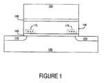
- FIG. 1shows a diagram of a non-volatile memory cell with a dielectric charge storage element.
- FIG. 2shows a memory cell array sector layout with a core memory cell array and a dynamic reference memory cell array in accordance with an embodiment of the present claimed invention.
- FIG. 3shows a read circuit with multiple reference cells in accordance with an embodiment of the present claimed invention.
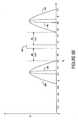
- FIG. 4Ashows an example of the threshold voltage (V t ) distributions in a memory cell array having a read margin of 0.3V using a common process for core and reference cell programming.
- FIG. 4Bshows an example of the threshold voltage V t distributions in a memory cell array having a read margin of 0.4V using a common process for core and reference cell programming.
- FIG. 4Cshows an example of the V t distributions in a memory cell array having a read margin of 0.5V using a common process for core and reference cell programming.
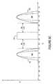
- FIG. 5Ashows an example of the V t distributions in a memory cell array with a core memory cell distribution width of 0.5V and a reference cell V t distribution width of 0.1 volt in accordance with an embodiment of the present claimed invention.
- FIG. 5Bshows an example of the V t distributions in a memory cell array with a core memory cell distribution width of 0.7V and a reference cell V t distribution width of 0.1 volt in accordance with an embodiment of the present claimed invention.
- FIG. 5Cshows an example of the V t distributions in a memory cell array with a core memory cell distribution width of 0.5V and a reference cell V t distribution width of 0.3 volt in accordance with an embodiment of the present claimed invention.
- FIG. 1shows a diagram of a memory cell with a dielectric storage element 160 .
- Symmetric source/drains 170are fabricated in a substrate 145 , and separated from the storage element 160 by an oxide 165 .
- the control gate 150is separated from the floating gate by an oxide 155 .
- a charge 175is transferred across the oxide 165 into the storage element 160 .
- the storage element 160may be injected with two distinct charges 175 , each located near a symmetric drain/source 170 .
- the charge transfermay be effected by Fowler-Nordheim tunneling or channel hot electron injection (CHE).
- CHEchannel hot electron injection
- FIG. 2shows an example of a memory cell array sector layout 200 .
- a sector 205comprises I/O blocks I/O 0 -I/O 15 that form the core memory array, reference blocks 215 and 220 , and a redundancy block 225 . As shown, the redundancy block may be physically separate from the remainder of the sector.
- Each I/O block 210comprises 4 sub-I/Os 230 , each with a width of 16 cells.
- Each sub-I/O(w 0 , w 1 , w 2 , w 3 ) has an associated word number (00, 01, 10, 11).
- the reference blocks 215 and 220 , and the Redundancy block 225are each 16 cells wide.
- the basic unit of width for the sector 205is 16 cells, and a common Y-decoder structure with an addressable width of 16 cells may be used to address each block.
- the total number of decoders requiredis 67, with 64 decoders for the 16 I/O blocks I/O 0 -I/O 15 , 2 decoders for the reference blocks 215 and 220 , and one decoder for the redundancy block 225 .
- the sector 205has an overall width of 1072 cells, and may have a height of about half of the width, e.g., 512 cells high.
- reference memory cellsin the same sector as the core memory cells, combined with dynamic programming, provide optimum tracking of the reference memory cells and core memory cells at beginning of life (BOL) and end of life (EOL).
- BOLbeginning of life
- EOLend of life
- the ratio of core cells to reference cellsis 32:1; however, other values may be used.
- a dynamic reference arraythe reference memory cells are programmed and erased in concert with the core memory cells that utilize the reference value provided by the dynamic reference array. This provides an automatic adjustment for changes in the memory cell behavior that is the result of aging (time/temperature) or the number of write/erase cycles.
- a dynamic reference arraymay be used for single-bit memory cells or multiple-bit memory cells. Dynamic reference arrays are particularly useful for flash memory devices that are fabricated using a process or design that has uniform aging characteristics, as opposed to catastrophic failure. For example, an oxide defect in a memory cell with a polysilicon floating gate may cause most of the stored charge to be lost, whereas in a cell with a dielectric storage element, the charge loss would be limited due to low charge mobility in the dielectric.
- FIG. 3shows a read circuit with multiple reference cells in accordance with an embodiment of the present invention.
- the read circuit 300comprises a non-volatile memory cell 305 coupled to a cascode circuit 315 by a Y-decoder 310 .
- the memory cell 305comprises a dielectric charge storage medium (e.g., an ONO layer).
- the read voltage signal 320is output from the cascode 315 to a first input of the sense amplifier 330 .
- a reference voltage signal 335is coupled to the second input of the sense amplifier 330 .
- the reference voltage signal 335is obtained from the combination of cascode 340 and cascode 365 .
- Cascode 345is coupled to a Y-decoder 350 and a first reference cell 355 .
- the signal from cascode 345may be switched by a transistor 340 .
- Cascode 370is coupled to a second reference cell 380 by a Y-decoder 375 .
- the signal from cascode 370may switched by a transistor 365 .
- the output of cascode 345 and cascode 370provide the reference voltage signal 335 to the sense amplifier 330 .
- the current to voltage conversion of the cascodes 345 and 370may also provide attenuation relative to the conversion of cascode 315 .
- cascode 345 and cascode 370may each provide 3 dB of attenuation, resulting in a combined output that is an average of their inputs when switches 340 and 365 are closed.
- reference cell 355is a reference “1”
- reference cell 380is a reference “0.”
- FIG. 4Ashows an example of the threshold voltage V t distributions in a memory cell array having a read margin of 0.3V using a common process for core and reference cell programming. Since a common process is used for programming, distribution 405 represents the identical V t distributions of the core and reference cells of the first state (e.g., 1), and distribution 410 represents the identical V t distributions of the second state (e.g., 0). Distribution 405 and 410 each have a width of 0.5V. It should be noted that the association of a logical value (0 or 1) with a particular V t is arbitrary.
- region 415represents the range of possible values for a reference value that is obtained from distributions 405 and 410 .
- the read margin M 1 in this caseis equal to 0.3V. It should be noted that the distributions shown are schematic, and are primarily intended to portray the width or limits of an actual distribution. No particular inference should be made from the shape of the curves, or the area underneath.
- FIG. 4Bshows an example of threshold voltage V t distributions similar to that of FIG. 4A, but with narrower distributions.
- distributions 405 and 410each have a width of 0.4V, providing a read margin M 2 of 0.4V. Since the core and reference distributions are narrower than those of FIG. 4A, the reference value range 430 is decreased and the read margin M 2 is increased.
- FIG. 4Cshows a further example of the effect of narrower V t distributions.
- the width of the core and reference V t distributions 435 and 440is 0.3V.
- the reference value range 445is reduced and the read margin M 3 is 0.5V.
- FIG. 5Ashows an example of the V t distributions in a memory cell array with a core memory cell distribution width of 0.5V and a reference cell V t distribution width of 0.1 volt in accordance with an embodiment of the present claimed invention.
- the core memory cellsare programmed with a process that produces a distribution width of 0.5V ( 505 , 515 ), similar to the core memory cell distribution of FIG. 4 A.
- decreasing the distribution width of the reference cell distribution ( 510 , 520 ) from 0.5V (FIG. 4A) to 0.1Vhas resulted in a decrease of the reference value range 525 to 0.2V and an increase of the read margin M 4 from 0.3V (FIG. 4A) to 0.5V.
- the narrower reference cell distributionis achieved by using a different programming pulse for programming the reference cells than that used for programming the core cells.
- the programming of the reference cellsmay be done with a finer programming pulse that is either shorter in duration, or smaller in amplitude, than the pulse used for programming the core cells.
- Programmingis typically done as an incremental operation with alternating write pulses and verify operations.
- the use of a shorter pulse, or lower voltage pulsewill reduce the incremental programming charge and thus reduce the width of the V t distribution.
- the use of a finer programming pulsemay also be applied to a write operation (e.g., soft programming) used to tailor or adjust erased cells.
- a programming process that uses a finer pulseis referred to as a finer programming process.
- the increase in overhead due to the use of a finer programming pulse for reference cellsis relatively small compared to the increase in read margin that is achieved.
- the programming of the core cells and reference cellsmay be done using the same basic write/verify algorithm, but with different pulse waveforms.
- the programming of the reference cellsmay be done using a different algorithm.
- core memory cellsmay be programmed with a pulse waveform that is unchanging during the write/verify cycle, whereas the reference cells are programmed with a pulse waveform that decreases in duration and/or amplitude during the write/verify cycle. If the core memory programming uses a variable pulse, the reference programming will use a variable pulse that is correspondingly finer.
- FIG. 5Bshows an example of the V t distributions in a memory cell array with a core memory cell distribution width of 0.7V ( 530 , 540 ) and a reference cell V t distribution width of 0.1V volt in accordance with an embodiment of the present claimed invention.
- the width of the core distribution ( 530 , 540 )is relaxed to 0.7V from the 0.5V of FIG. 5 A.
- the read margin M 5is still 0.4V. This compares favorably to the scheme of FIG. 4A in which the core distribution width is 0.5V ( 405 , 410 ) and the read margin M 1 only 0.3V.
- FIG. 5Cshows an example of the V t distributions in a memory cell array with a core memory cell distribution width of 0.5V ( 555 , 565 ) and a reference cell V t distribution width of 0.3V volt in accordance with an embodiment of the present claimed invention.
- the width of the reference distribution( 560 , 570 ) is relaxed to 0.3V from the 0.1V of FIG. 5 A.
- the read margin M 6is still 0.4V. This compares favorably to the scheme of FIG. 4A in which the core distribution width is 0.5V ( 405 , 410 ) and the read margin M 1 only 0.3V.
- the V t distributions for the two stateswere shown as being the same. In practice, the distributions of the two states may have different characteristics. Also, the use of two different programming processes for the core and reference cells may be restricted to one memory cell state. Although the largest improvement in read margin is achieved by narrowing the reference array V t distribution for both states, it may be desirable to limit the fine pulse programming of the reference array to one of the two states.
Landscapes
- Engineering & Computer Science (AREA)
- Computer Hardware Design (AREA)
- Microelectronics & Electronic Packaging (AREA)
- Read Only Memory (AREA)
Abstract
Description
Claims (20)
Priority Applications (1)
| Application Number | Priority Date | Filing Date | Title |
|---|---|---|---|
| US10/349,293US6643177B1 (en) | 2003-01-21 | 2003-01-21 | Method for improving read margin in a flash memory device |
Applications Claiming Priority (1)
| Application Number | Priority Date | Filing Date | Title |
|---|---|---|---|
| US10/349,293US6643177B1 (en) | 2003-01-21 | 2003-01-21 | Method for improving read margin in a flash memory device |
Publications (1)
| Publication Number | Publication Date |
|---|---|
| US6643177B1true US6643177B1 (en) | 2003-11-04 |
Family
ID=29270461
Family Applications (1)
| Application Number | Title | Priority Date | Filing Date |
|---|---|---|---|
| US10/349,293Expired - LifetimeUS6643177B1 (en) | 2003-01-21 | 2003-01-21 | Method for improving read margin in a flash memory device |
Country Status (1)
| Country | Link |
|---|---|
| US (1) | US6643177B1 (en) |
Cited By (53)
| Publication number | Priority date | Publication date | Assignee | Title |
|---|---|---|---|---|
| US20040257873A1 (en)* | 2003-06-20 | 2004-12-23 | Ming-Huei Shieh | Memory with a core-based virtual ground and dynamic reference sensing scheme |
| US20050058005A1 (en)* | 2002-01-31 | 2005-03-17 | Assaf Shappir | Method for operating a memory device |
| US6917544B2 (en) | 2002-07-10 | 2005-07-12 | Saifun Semiconductors Ltd. | Multiple use memory chip |
| US6928001B2 (en) | 2000-12-07 | 2005-08-09 | Saifun Semiconductors Ltd. | Programming and erasing methods for a non-volatile memory cell |
| US20050190603A1 (en)* | 2004-02-26 | 2005-09-01 | Seung-Keun Lee | Multi level flash memory device and program method |
| US6967896B2 (en) | 2003-01-30 | 2005-11-22 | Saifun Semiconductors Ltd | Address scramble |
| US20050270848A1 (en)* | 2004-06-07 | 2005-12-08 | Dong-Hyuk Chae | Non-volatile memory device capable of changing increment of program voltage according to mode of operation |
| US6982905B2 (en) | 2003-10-09 | 2006-01-03 | Micron Technology, Inc. | Method and apparatus for reading NAND flash memory array |
| US20060109718A1 (en)* | 2004-11-24 | 2006-05-25 | Macronix International Co., Ltd. | System and method for preventing read margin degradation for a memory array |
| US7064983B2 (en) | 2001-04-05 | 2006-06-20 | Saifum Semiconductors Ltd. | Method for programming a reference cell |
| US20060164887A1 (en)* | 2005-01-26 | 2006-07-27 | Macronix International Co., Ltd. | Method and apparatus for changing operating conditions of nonvolatile memory |
| US7136304B2 (en) | 2002-10-29 | 2006-11-14 | Saifun Semiconductor Ltd | Method, system and circuit for programming a non-volatile memory array |
| US20060289906A1 (en)* | 2001-09-19 | 2006-12-28 | Renesas Technology Corp. | Semiconductor device including a capacitance |
| US7184313B2 (en) | 2005-06-17 | 2007-02-27 | Saifun Semiconductors Ltd. | Method circuit and system for compensating for temperature induced margin loss in non-volatile memory cells |
| US7190620B2 (en) | 2002-01-31 | 2007-03-13 | Saifun Semiconductors Ltd. | Method for operating a memory device |
| US7221138B2 (en) | 2005-09-27 | 2007-05-22 | Saifun Semiconductors Ltd | Method and apparatus for measuring charge pump output current |
| US20070183210A1 (en)* | 2006-02-01 | 2007-08-09 | Choi Ki-Hwan | Program method of flash memory capable of compensating read margin reduced due to charge loss |
| US7317633B2 (en) | 2004-07-06 | 2008-01-08 | Saifun Semiconductors Ltd | Protection of NROM devices from charge damage |
| US20080013379A1 (en)* | 2006-07-14 | 2008-01-17 | Macronix International Co., Ltd. | Method and apparatus for reading data from nonvolatile memory |
| US20080037329A1 (en)* | 2005-03-28 | 2008-02-14 | Motoi Takahashi | Nonvolatile semiconductor memory, method for reading the same, and microprocessor |
| US20080056053A1 (en)* | 2006-08-31 | 2008-03-06 | Setti Shanmukheswara Rao | Word line control method to improve read margin and write margin for embedded memories |
| US7352627B2 (en) | 2006-01-03 | 2008-04-01 | Saifon Semiconductors Ltd. | Method, system, and circuit for operating a non-volatile memory array |
| US7366025B2 (en) | 2004-06-10 | 2008-04-29 | Saifun Semiconductors Ltd. | Reduced power programming of non-volatile cells |
| US7369440B2 (en) | 2005-01-19 | 2008-05-06 | Saifun Semiconductors Ltd. | Method, circuit and systems for erasing one or more non-volatile memory cells |
| US7405969B2 (en) | 1997-08-01 | 2008-07-29 | Saifun Semiconductors Ltd. | Non-volatile memory cell and non-volatile memory devices |
| US7457183B2 (en) | 2003-09-16 | 2008-11-25 | Saifun Semiconductors Ltd. | Operating array cells with matched reference cells |
| US7466594B2 (en) | 2004-08-12 | 2008-12-16 | Saifun Semiconductors Ltd. | Dynamic matching of signal path and reference path for sensing |
| US20090091974A1 (en)* | 2007-10-08 | 2009-04-09 | Samsung Electronics Co., Ltd. | Methods of programming non-volatile memory cells |
| US7532529B2 (en) | 2004-03-29 | 2009-05-12 | Saifun Semiconductors Ltd. | Apparatus and methods for multi-level sensing in a memory array |
| US7535765B2 (en) | 2004-12-09 | 2009-05-19 | Saifun Semiconductors Ltd. | Non-volatile memory device and method for reading cells |
| US7605579B2 (en) | 2006-09-18 | 2009-10-20 | Saifun Semiconductors Ltd. | Measuring and controlling current consumption and output current of charge pumps |
| US7638850B2 (en) | 2004-10-14 | 2009-12-29 | Saifun Semiconductors Ltd. | Non-volatile memory structure and method of fabrication |
| US7638835B2 (en) | 2006-02-28 | 2009-12-29 | Saifun Semiconductors Ltd. | Double density NROM with nitride strips (DDNS) |
| US7652930B2 (en) | 2004-04-01 | 2010-01-26 | Saifun Semiconductors Ltd. | Method, circuit and system for erasing one or more non-volatile memory cells |
| US7668017B2 (en) | 2005-08-17 | 2010-02-23 | Saifun Semiconductors Ltd. | Method of erasing non-volatile memory cells |
| US7692961B2 (en) | 2006-02-21 | 2010-04-06 | Saifun Semiconductors Ltd. | Method, circuit and device for disturb-control of programming nonvolatile memory cells by hot-hole injection (HHI) and by channel hot-electron (CHE) injection |
| US7701779B2 (en) | 2006-04-27 | 2010-04-20 | Sajfun Semiconductors Ltd. | Method for programming a reference cell |
| US7743230B2 (en) | 2003-01-31 | 2010-06-22 | Saifun Semiconductors Ltd. | Memory array programming circuit and a method for using the circuit |
| US7760554B2 (en) | 2006-02-21 | 2010-07-20 | Saifun Semiconductors Ltd. | NROM non-volatile memory and mode of operation |
| US7786512B2 (en) | 2005-07-18 | 2010-08-31 | Saifun Semiconductors Ltd. | Dense non-volatile memory array and method of fabrication |
| US7808818B2 (en) | 2006-01-12 | 2010-10-05 | Saifun Semiconductors Ltd. | Secondary injection for NROM |
| US8053812B2 (en) | 2005-03-17 | 2011-11-08 | Spansion Israel Ltd | Contact in planar NROM technology |
| US8253452B2 (en) | 2006-02-21 | 2012-08-28 | Spansion Israel Ltd | Circuit and method for powering up an integrated circuit and an integrated circuit utilizing same |
| US8400841B2 (en) | 2005-06-15 | 2013-03-19 | Spansion Israel Ltd. | Device to program adjacent storage cells of different NROM cells |
| US20130242669A1 (en)* | 2012-03-18 | 2013-09-19 | Spansion Israel Ltd | End-of-life reliability for non-volatile memory cells |
| US8737141B2 (en) | 2010-07-07 | 2014-05-27 | Stec, Inc. | Apparatus and method for determining an operating condition of a memory cell based on cycle information |
| US8737136B2 (en) | 2010-07-09 | 2014-05-27 | Stec, Inc. | Apparatus and method for determining a read level of a memory cell based on cycle information |
| US8755229B1 (en) | 2009-06-23 | 2014-06-17 | Micron Technology, Inc. | Limiting flash memory over programming |
| US8819503B2 (en) | 2010-07-02 | 2014-08-26 | Stec, Inc. | Apparatus and method for determining an operating condition of a memory cell based on cycle information |
| US9047955B2 (en) | 2011-03-30 | 2015-06-02 | Stec, Inc. | Adjusting operating parameters for memory cells based on wordline address and cycle information |
| US9195586B2 (en) | 2012-02-23 | 2015-11-24 | Hgst Technologies Santa Ana, Inc. | Determining bias information for offsetting operating variations in memory cells based on wordline address |
| US9778851B2 (en) | 2015-12-03 | 2017-10-03 | Samsung Electronics Co., Ltd. | Method of operation for a nonvolatile memory system and method of operating a memory controller |
| US12205633B2 (en) | 2022-06-14 | 2025-01-21 | Globalfoundries U.S. Inc. | Non-volatile memory device with reference voltage circuit including column(s) of reference bit cells adjacent columns of memory bit cells within a memory cell array |
Citations (1)
| Publication number | Priority date | Publication date | Assignee | Title |
|---|---|---|---|---|
| US6519184B2 (en)* | 2001-04-19 | 2003-02-11 | Hitachi, Ltd. | Non-volatile memory device with plurality of threshold voltage distributions |
- 2003
- 2003-01-21USUS10/349,293patent/US6643177B1/ennot_activeExpired - Lifetime
Patent Citations (1)
| Publication number | Priority date | Publication date | Assignee | Title |
|---|---|---|---|---|
| US6519184B2 (en)* | 2001-04-19 | 2003-02-11 | Hitachi, Ltd. | Non-volatile memory device with plurality of threshold voltage distributions |
Cited By (87)
| Publication number | Priority date | Publication date | Assignee | Title |
|---|---|---|---|---|
| US7405969B2 (en) | 1997-08-01 | 2008-07-29 | Saifun Semiconductors Ltd. | Non-volatile memory cell and non-volatile memory devices |
| US6937521B2 (en) | 2000-05-04 | 2005-08-30 | Saifun Semiconductors Ltd. | Programming and erasing methods for a non-volatile memory cell |
| US6928001B2 (en) | 2000-12-07 | 2005-08-09 | Saifun Semiconductors Ltd. | Programming and erasing methods for a non-volatile memory cell |
| US7064983B2 (en) | 2001-04-05 | 2006-06-20 | Saifum Semiconductors Ltd. | Method for programming a reference cell |
| US20060289906A1 (en)* | 2001-09-19 | 2006-12-28 | Renesas Technology Corp. | Semiconductor device including a capacitance |
| US7420848B2 (en) | 2002-01-31 | 2008-09-02 | Saifun Semiconductors Ltd. | Method, system, and circuit for operating a non-volatile memory array |
| US7190620B2 (en) | 2002-01-31 | 2007-03-13 | Saifun Semiconductors Ltd. | Method for operating a memory device |
| US20050058005A1 (en)* | 2002-01-31 | 2005-03-17 | Assaf Shappir | Method for operating a memory device |
| US7079420B2 (en) | 2002-01-31 | 2006-07-18 | Saifun Semiconductors Ltd. | Method for operating a memory device |
| US7738304B2 (en) | 2002-07-10 | 2010-06-15 | Saifun Semiconductors Ltd. | Multiple use memory chip |
| US6917544B2 (en) | 2002-07-10 | 2005-07-12 | Saifun Semiconductors Ltd. | Multiple use memory chip |
| US7136304B2 (en) | 2002-10-29 | 2006-11-14 | Saifun Semiconductor Ltd | Method, system and circuit for programming a non-volatile memory array |
| US7675782B2 (en) | 2002-10-29 | 2010-03-09 | Saifun Semiconductors Ltd. | Method, system and circuit for programming a non-volatile memory array |
| US6967896B2 (en) | 2003-01-30 | 2005-11-22 | Saifun Semiconductors Ltd | Address scramble |
| US7743230B2 (en) | 2003-01-31 | 2010-06-22 | Saifun Semiconductors Ltd. | Memory array programming circuit and a method for using the circuit |
| US20080117678A1 (en)* | 2003-06-20 | 2008-05-22 | Spansion Llc | Memory with a core-based virtual ground and dynamic reference sensing scheme |
| US7606068B2 (en) | 2003-06-20 | 2009-10-20 | Spansion Llc | Memory with a core-based virtual ground and dynamic reference sensing scheme |
| US7324374B2 (en)* | 2003-06-20 | 2008-01-29 | Spansion Llc | Memory with a core-based virtual ground and dynamic reference sensing scheme |
| US20040257873A1 (en)* | 2003-06-20 | 2004-12-23 | Ming-Huei Shieh | Memory with a core-based virtual ground and dynamic reference sensing scheme |
| US7457183B2 (en) | 2003-09-16 | 2008-11-25 | Saifun Semiconductors Ltd. | Operating array cells with matched reference cells |
| US6982905B2 (en) | 2003-10-09 | 2006-01-03 | Micron Technology, Inc. | Method and apparatus for reading NAND flash memory array |
| US7203093B2 (en) | 2003-10-09 | 2007-04-10 | Micron Technology, Inc. | Method and apparatus for reading NAND flash memory array |
| US20060034119A1 (en)* | 2003-10-09 | 2006-02-16 | Micron Technology, Inc. | Method and apparatus for reading nand flash memory array |
| US7054199B2 (en)* | 2004-02-26 | 2006-05-30 | Samsung Electronics Co., Ltd. | Multi level flash memory device and program method |
| US20050190603A1 (en)* | 2004-02-26 | 2005-09-01 | Seung-Keun Lee | Multi level flash memory device and program method |
| US7532529B2 (en) | 2004-03-29 | 2009-05-12 | Saifun Semiconductors Ltd. | Apparatus and methods for multi-level sensing in a memory array |
| US7652930B2 (en) | 2004-04-01 | 2010-01-26 | Saifun Semiconductors Ltd. | Method, circuit and system for erasing one or more non-volatile memory cells |
| US20070076488A1 (en)* | 2004-06-07 | 2007-04-05 | Samsung Electronics Co., Ltd. | Non-volatile memory device capable of changing increment of program voltage according to mode of operation |
| US7158418B2 (en) | 2004-06-07 | 2007-01-02 | Samsung Electronics Co., Ltd. | Non-volatile memory device capable of changing increment of program voltage to mode of operation |
| US7474564B2 (en) | 2004-06-07 | 2009-01-06 | Samsung Electronics Co., Ltd. | Non-volatile memory device capable of changing increment of program voltage according to mode of operation |
| US20050270848A1 (en)* | 2004-06-07 | 2005-12-08 | Dong-Hyuk Chae | Non-volatile memory device capable of changing increment of program voltage according to mode of operation |
| US7366025B2 (en) | 2004-06-10 | 2008-04-29 | Saifun Semiconductors Ltd. | Reduced power programming of non-volatile cells |
| US7317633B2 (en) | 2004-07-06 | 2008-01-08 | Saifun Semiconductors Ltd | Protection of NROM devices from charge damage |
| US7466594B2 (en) | 2004-08-12 | 2008-12-16 | Saifun Semiconductors Ltd. | Dynamic matching of signal path and reference path for sensing |
| US7964459B2 (en) | 2004-10-14 | 2011-06-21 | Spansion Israel Ltd. | Non-volatile memory structure and method of fabrication |
| US7638850B2 (en) | 2004-10-14 | 2009-12-29 | Saifun Semiconductors Ltd. | Non-volatile memory structure and method of fabrication |
| US20060109718A1 (en)* | 2004-11-24 | 2006-05-25 | Macronix International Co., Ltd. | System and method for preventing read margin degradation for a memory array |
| US7262999B2 (en) | 2004-11-24 | 2007-08-28 | Macronix International Co., Ltd. | System and method for preventing read margin degradation for a memory array |
| CN100490013C (en)* | 2004-11-24 | 2009-05-20 | 旺宏电子股份有限公司 | System and method for preventing read margin reduction of memory array |
| US7535765B2 (en) | 2004-12-09 | 2009-05-19 | Saifun Semiconductors Ltd. | Non-volatile memory device and method for reading cells |
| US7369440B2 (en) | 2005-01-19 | 2008-05-06 | Saifun Semiconductors Ltd. | Method, circuit and systems for erasing one or more non-volatile memory cells |
| US7468926B2 (en) | 2005-01-19 | 2008-12-23 | Saifun Semiconductors Ltd. | Partial erase verify |
| US20060164887A1 (en)* | 2005-01-26 | 2006-07-27 | Macronix International Co., Ltd. | Method and apparatus for changing operating conditions of nonvolatile memory |
| US7149121B2 (en) | 2005-01-26 | 2006-12-12 | Macronix International Co., Ltd. | Method and apparatus for changing operating conditions of nonvolatile memory |
| US8053812B2 (en) | 2005-03-17 | 2011-11-08 | Spansion Israel Ltd | Contact in planar NROM technology |
| US7773425B2 (en)* | 2005-03-28 | 2010-08-10 | Fujitsu Semiconductor Limited | Nonvolatile semiconductor memory, method for reading the same, and microprocessor |
| US20080037329A1 (en)* | 2005-03-28 | 2008-02-14 | Motoi Takahashi | Nonvolatile semiconductor memory, method for reading the same, and microprocessor |
| US8400841B2 (en) | 2005-06-15 | 2013-03-19 | Spansion Israel Ltd. | Device to program adjacent storage cells of different NROM cells |
| US7184313B2 (en) | 2005-06-17 | 2007-02-27 | Saifun Semiconductors Ltd. | Method circuit and system for compensating for temperature induced margin loss in non-volatile memory cells |
| US7786512B2 (en) | 2005-07-18 | 2010-08-31 | Saifun Semiconductors Ltd. | Dense non-volatile memory array and method of fabrication |
| US7668017B2 (en) | 2005-08-17 | 2010-02-23 | Saifun Semiconductors Ltd. | Method of erasing non-volatile memory cells |
| US7221138B2 (en) | 2005-09-27 | 2007-05-22 | Saifun Semiconductors Ltd | Method and apparatus for measuring charge pump output current |
| US7352627B2 (en) | 2006-01-03 | 2008-04-01 | Saifon Semiconductors Ltd. | Method, system, and circuit for operating a non-volatile memory array |
| US7808818B2 (en) | 2006-01-12 | 2010-10-05 | Saifun Semiconductors Ltd. | Secondary injection for NROM |
| US7489558B2 (en) | 2006-02-01 | 2009-02-10 | Samsung Electronics Co., Ltd. | Program method of flash memory capable of compensating read margin reduced due to charge loss |
| US20070183210A1 (en)* | 2006-02-01 | 2007-08-09 | Choi Ki-Hwan | Program method of flash memory capable of compensating read margin reduced due to charge loss |
| US7692961B2 (en) | 2006-02-21 | 2010-04-06 | Saifun Semiconductors Ltd. | Method, circuit and device for disturb-control of programming nonvolatile memory cells by hot-hole injection (HHI) and by channel hot-electron (CHE) injection |
| US8253452B2 (en) | 2006-02-21 | 2012-08-28 | Spansion Israel Ltd | Circuit and method for powering up an integrated circuit and an integrated circuit utilizing same |
| US7760554B2 (en) | 2006-02-21 | 2010-07-20 | Saifun Semiconductors Ltd. | NROM non-volatile memory and mode of operation |
| US7638835B2 (en) | 2006-02-28 | 2009-12-29 | Saifun Semiconductors Ltd. | Double density NROM with nitride strips (DDNS) |
| US7701779B2 (en) | 2006-04-27 | 2010-04-20 | Sajfun Semiconductors Ltd. | Method for programming a reference cell |
| US7339846B2 (en) | 2006-07-14 | 2008-03-04 | Macronix International Co., Ltd. | Method and apparatus for reading data from nonvolatile memory |
| US20080013379A1 (en)* | 2006-07-14 | 2008-01-17 | Macronix International Co., Ltd. | Method and apparatus for reading data from nonvolatile memory |
| US20080056053A1 (en)* | 2006-08-31 | 2008-03-06 | Setti Shanmukheswara Rao | Word line control method to improve read margin and write margin for embedded memories |
| US7558145B2 (en) | 2006-08-31 | 2009-07-07 | Infineon Technologies Ag | Word line control for improving read and write margins |
| US7605579B2 (en) | 2006-09-18 | 2009-10-20 | Saifun Semiconductors Ltd. | Measuring and controlling current consumption and output current of charge pumps |
| US7885107B2 (en)* | 2007-10-08 | 2011-02-08 | Samsung Electronics Co, Ltd. | Methods of programming non-volatile memory cells |
| US20090091974A1 (en)* | 2007-10-08 | 2009-04-09 | Samsung Electronics Co., Ltd. | Methods of programming non-volatile memory cells |
| US11430522B2 (en) | 2009-06-23 | 2022-08-30 | Micron Technology, Inc. | Programming of memory devices |
| US10811098B2 (en) | 2009-06-23 | 2020-10-20 | Micron Technology, Inc. | Programming of memory devices in response to programming voltages indicative of programming efficiency |
| US10586597B2 (en) | 2009-06-23 | 2020-03-10 | Micron Technology, Inc. | Programming of memory devices responsive to a stored representation of a programming voltage indicative of a programming efficiency |
| US8755229B1 (en) | 2009-06-23 | 2014-06-17 | Micron Technology, Inc. | Limiting flash memory over programming |
| US10074432B2 (en) | 2009-06-23 | 2018-09-11 | Micron Technology, Inc. | Programming of memory devices |
| US9142314B2 (en) | 2009-06-23 | 2015-09-22 | Micron Technology, Inc. | Limiting flash memory over programming |
| US8819503B2 (en) | 2010-07-02 | 2014-08-26 | Stec, Inc. | Apparatus and method for determining an operating condition of a memory cell based on cycle information |
| US9389938B2 (en) | 2010-07-07 | 2016-07-12 | Hgst Technologies Santa Ana, Inc. | Apparatus and method for determining an operating condition of a memory cell based on cycle information |
| US8737141B2 (en) | 2010-07-07 | 2014-05-27 | Stec, Inc. | Apparatus and method for determining an operating condition of a memory cell based on cycle information |
| US8737136B2 (en) | 2010-07-09 | 2014-05-27 | Stec, Inc. | Apparatus and method for determining a read level of a memory cell based on cycle information |
| US9224456B2 (en) | 2011-03-30 | 2015-12-29 | Hgst Technologies Santa Ana, Inc. | Setting operating parameters for memory cells based on wordline address and cycle information |
| US9047955B2 (en) | 2011-03-30 | 2015-06-02 | Stec, Inc. | Adjusting operating parameters for memory cells based on wordline address and cycle information |
| US9377962B2 (en) | 2012-02-23 | 2016-06-28 | Hgst Technologies Santa Ana, Inc. | Determining bias information for offsetting operating variations in memory cells |
| US9195586B2 (en) | 2012-02-23 | 2015-11-24 | Hgst Technologies Santa Ana, Inc. | Determining bias information for offsetting operating variations in memory cells based on wordline address |
| US9543017B2 (en)* | 2012-03-18 | 2017-01-10 | Cypress Semiconductors Ltd. | End-of-life reliability for non-volatile memory cells |
| US20130242669A1 (en)* | 2012-03-18 | 2013-09-19 | Spansion Israel Ltd | End-of-life reliability for non-volatile memory cells |
| US9778851B2 (en) | 2015-12-03 | 2017-10-03 | Samsung Electronics Co., Ltd. | Method of operation for a nonvolatile memory system and method of operating a memory controller |
| US10089016B2 (en) | 2015-12-03 | 2018-10-02 | Samsung Electronics Co., Ltd. | Method of operation for a nonvolatile memory system and method of operating a memory controller |
| US12205633B2 (en) | 2022-06-14 | 2025-01-21 | Globalfoundries U.S. Inc. | Non-volatile memory device with reference voltage circuit including column(s) of reference bit cells adjacent columns of memory bit cells within a memory cell array |
Similar Documents
| Publication | Publication Date | Title |
|---|---|---|
| US6643177B1 (en) | Method for improving read margin in a flash memory device | |
| US6771540B2 (en) | Nonvolatile semiconductor storage device and method for operating the device | |
| US6456528B1 (en) | Selective operation of a multi-state non-volatile memory system in a binary mode | |
| US6777292B2 (en) | Set of three level concurrent word line bias conditions for a NOR type flash memory array | |
| JP3796457B2 (en) | Nonvolatile semiconductor memory device | |
| US7385854B2 (en) | Selective operation of a multi-state non-volatile memory system in a binary mode | |
| KR100935948B1 (en) | Algorithm Dynamic Reference Programming | |
| KR101030680B1 (en) | Current Limit Latch Circuit | |
| US6643185B1 (en) | Method for repairing over-erasure of fast bits on floating gate memory devices | |
| US20030012064A1 (en) | Method of refreshing an electrically erasable and programmable non-volatile memory | |
| US6791880B1 (en) | Non-volatile memory read circuit with end of life simulation | |
| US6856552B2 (en) | Semiconductor memory and method of driving the same | |
| KR20080033460A (en) | System and method for programming a cell in a nonvolatile integrated memory device | |
| KR20060002759A (en) | System and method for programming a cell in a nonvolatile memory device | |
| US5521867A (en) | Adjustable threshold voltage conversion circuit | |
| JP3974778B2 (en) | Nonvolatile semiconductor memory device and data erasing method thereof | |
| JP4104151B2 (en) | Nonvolatile semiconductor memory device and method for programming nonvolatile semiconductor memory device | |
| US7929353B2 (en) | Method and apparatus for adaptive memory cell overerase compensation | |
| KR100629193B1 (en) | Nonvolatile semiconductor memory device and recording method thereof | |
| US7933150B2 (en) | Nonvolatile semiconductor memory device and programming method thereof | |
| US6934190B1 (en) | Ramp source hot-hole programming for trap based non-volatile memory devices | |
| US7570514B2 (en) | Method of operating multi-level cell and integrate circuit for using multi-level cell to store data | |
| EP1763039B1 (en) | Method and apparatus for protection from over-erasing nonvolatile memory cells | |
| US7142455B1 (en) | Positive gate stress during erase to improve retention in multi-level, non-volatile flash memory | |
| US6847548B2 (en) | Memory with multiple state cells and sensing method |
Legal Events
| Date | Code | Title | Description |
|---|---|---|---|
| AS | Assignment | Owner name:ADVANCED MICRO DEVICES INC., CALIFORNIA Free format text:ASSIGNMENT OF ASSIGNORS INTEREST;ASSIGNORS:LE, BINH QUANG;CHEN, PAU-LING;REEL/FRAME:013696/0135;SIGNING DATES FROM 20030110 TO 20030115 | |
| STCF | Information on status: patent grant | Free format text:PATENTED CASE | |
| FEPP | Fee payment procedure | Free format text:PAYOR NUMBER ASSIGNED (ORIGINAL EVENT CODE: ASPN); ENTITY STATUS OF PATENT OWNER: LARGE ENTITY | |
| FPAY | Fee payment | Year of fee payment:4 | |
| AS | Assignment | Owner name:SPANSION INC., CALIFORNIA Free format text:ASSIGNMENT OF ASSIGNORS INTEREST;ASSIGNOR:ADVANCED MICRO DEVICES, INC.;REEL/FRAME:019047/0588 Effective date:20070131 | |
| AS | Assignment | Owner name:SPANSION LLC, CALIFORNIA Free format text:ASSIGNMENT OF ASSIGNORS INTEREST;ASSIGNOR:SPANSION INC.;REEL/FRAME:019069/0342 Effective date:20070131 | |
| AS | Assignment | Owner name:BARCLAYS BANK PLC,NEW YORK Free format text:SECURITY AGREEMENT;ASSIGNORS:SPANSION LLC;SPANSION INC.;SPANSION TECHNOLOGY INC.;AND OTHERS;REEL/FRAME:024522/0338 Effective date:20100510 Owner name:BARCLAYS BANK PLC, NEW YORK Free format text:SECURITY AGREEMENT;ASSIGNORS:SPANSION LLC;SPANSION INC.;SPANSION TECHNOLOGY INC.;AND OTHERS;REEL/FRAME:024522/0338 Effective date:20100510 | |
| FPAY | Fee payment | Year of fee payment:8 | |
| AS | Assignment | Owner name:SPANSION INC., CALIFORNIA Free format text:RELEASE BY SECURED PARTY;ASSIGNOR:BARCLAYS BANK PLC;REEL/FRAME:035201/0159 Effective date:20150312 Owner name:SPANSION TECHNOLOGY LLC, CALIFORNIA Free format text:RELEASE BY SECURED PARTY;ASSIGNOR:BARCLAYS BANK PLC;REEL/FRAME:035201/0159 Effective date:20150312 Owner name:SPANSION LLC, CALIFORNIA Free format text:RELEASE BY SECURED PARTY;ASSIGNOR:BARCLAYS BANK PLC;REEL/FRAME:035201/0159 Effective date:20150312 | |
| AS | Assignment | Owner name:MORGAN STANLEY SENIOR FUNDING, INC., NEW YORK Free format text:SECURITY INTEREST;ASSIGNORS:CYPRESS SEMICONDUCTOR CORPORATION;SPANSION LLC;REEL/FRAME:035240/0429 Effective date:20150312 | |
| REMI | Maintenance fee reminder mailed | ||
| FPAY | Fee payment | Year of fee payment:12 | |
| SULP | Surcharge for late payment | Year of fee payment:11 | |
| AS | Assignment | Owner name:CYPRESS SEMICONDUCTOR CORPORATION, CALIFORNIA Free format text:ASSIGNMENT OF ASSIGNORS INTEREST;ASSIGNOR:SPANSION, LLC;REEL/FRAME:036032/0001 Effective date:20150601 | |
| AS | Assignment | Owner name:MONTEREY RESEARCH, LLC, CALIFORNIA Free format text:ASSIGNMENT OF ASSIGNORS INTEREST;ASSIGNOR:CYPRESS SEMICONDUCTOR CORPORATION;REEL/FRAME:044938/0360 Effective date:20171218 | |
| AS | Assignment | Owner name:SPANSION LLC, CALIFORNIA Free format text:RELEASE BY SECURED PARTY;ASSIGNOR:MORGAN STANLEY SENIOR FUNDING, INC;REEL/FRAME:044949/0962 Effective date:20171218 Owner name:CYPRESS SEMICONDUCTOR CORPORATION, CALIFORNIA Free format text:RELEASE BY SECURED PARTY;ASSIGNOR:MORGAN STANLEY SENIOR FUNDING, INC;REEL/FRAME:044949/0962 Effective date:20171218 | |
| AS | Assignment | Owner name:MORGAN STANLEY SENIOR FUNDING, INC., NEW YORK Free format text:CORRECTIVE ASSIGNMENT TO CORRECT THE 8647899 PREVIOUSLY RECORDED ON REEL 035240 FRAME 0429. ASSIGNOR(S) HEREBY CONFIRMS THE SECURITY INTERST;ASSIGNORS:CYPRESS SEMICONDUCTOR CORPORATION;SPANSION LLC;REEL/FRAME:058002/0470 Effective date:20150312 |