US6642913B1 - Light modulation element, exposure unit, and flat-panel display unit - Google Patents
Light modulation element, exposure unit, and flat-panel display unitDownload PDFInfo
- Publication number
- US6642913B1 US6642913B1US09/487,296US48729600AUS6642913B1US 6642913 B1US6642913 B1US 6642913B1US 48729600 AUS48729600 AUS 48729600AUS 6642913 B1US6642913 B1US 6642913B1
- Authority
- US
- United States
- Prior art keywords
- light
- light modulation
- thin film
- flexible thin
- modulation element
- Prior art date
- Legal status (The legal status is an assumption and is not a legal conclusion. Google has not performed a legal analysis and makes no representation as to the accuracy of the status listed.)
- Expired - Fee Related
Links
- 239000010409thin filmSubstances0.000claimsabstractdescription147
- 239000000463materialSubstances0.000claimsdescription124
- 230000003287optical effectEffects0.000claimsdescription57
- 239000010408filmSubstances0.000claimsdescription28
- 239000011159matrix materialSubstances0.000claimsdescription25
- 239000011347resinSubstances0.000claimsdescription12
- 229920005989resinPolymers0.000claimsdescription12
- 239000010419fine particleSubstances0.000claimsdescription9
- 239000000758substrateSubstances0.000claimsdescription9
- 239000000049pigmentSubstances0.000claimsdescription8
- 239000003086colorantSubstances0.000claimsdescription7
- 239000007850fluorescent dyeSubstances0.000claimsdescription5
- 230000007246mechanismEffects0.000claimsdescription3
- OAICVXFJPJFONN-UHFFFAOYSA-NPhosphorusChemical compound[P]OAICVXFJPJFONN-UHFFFAOYSA-N0.000abstract2
- 238000000034methodMethods0.000description13
- 230000015572biosynthetic processEffects0.000description12
- 125000006850spacer groupChemical group0.000description11
- 238000004519manufacturing processMethods0.000description10
- 230000002708enhancing effectEffects0.000description7
- 230000000644propagated effectEffects0.000description7
- 239000002184metalSubstances0.000description5
- XLOMVQKBTHCTTD-UHFFFAOYSA-NZinc monoxideChemical compound[Zn]=OXLOMVQKBTHCTTD-UHFFFAOYSA-N0.000description4
- 230000000694effectsEffects0.000description4
- 239000011521glassSubstances0.000description4
- 239000004973liquid crystal related substanceSubstances0.000description4
- 229910052751metalInorganic materials0.000description4
- 229910052782aluminiumInorganic materials0.000description3
- XAGFODPZIPBFFR-UHFFFAOYSA-NaluminiumChemical compound[Al]XAGFODPZIPBFFR-UHFFFAOYSA-N0.000description3
- 230000008569processEffects0.000description3
- KDLHZDBZIXYQEI-UHFFFAOYSA-NPalladiumChemical compound[Pd]KDLHZDBZIXYQEI-UHFFFAOYSA-N0.000description2
- VYPSYNLAJGMNEJ-UHFFFAOYSA-NSilicium dioxideChemical compoundO=[Si]=OVYPSYNLAJGMNEJ-UHFFFAOYSA-N0.000description2
- 239000000919ceramicSubstances0.000description2
- 230000008859changeEffects0.000description2
- 238000010586diagramMethods0.000description2
- 238000005516engineering processMethods0.000description2
- 238000005530etchingMethods0.000description2
- QSHDDOUJBYECFT-UHFFFAOYSA-NmercuryChemical compound[Hg]QSHDDOUJBYECFT-UHFFFAOYSA-N0.000description2
- 229910052753mercuryInorganic materials0.000description2
- 150000002736metal compoundsChemical class0.000description2
- 229910044991metal oxideInorganic materials0.000description2
- 150000004706metal oxidesChemical class0.000description2
- 150000004767nitridesChemical class0.000description2
- 239000004065semiconductorSubstances0.000description2
- 229910052814silicon oxideInorganic materials0.000description2
- 239000007921spraySubstances0.000description2
- XOLBLPGZBRYERU-UHFFFAOYSA-Ntin dioxideChemical compoundO=[Sn]=OXOLBLPGZBRYERU-UHFFFAOYSA-N0.000description2
- 239000011787zinc oxideSubstances0.000description2
- NCGICGYLBXGBGN-UHFFFAOYSA-N3-morpholin-4-yl-1-oxa-3-azonia-2-azanidacyclopent-3-en-5-imine;hydrochlorideChemical compoundCl.[N-]1OC(=N)C=[N+]1N1CCOCC1NCGICGYLBXGBGN-UHFFFAOYSA-N0.000description1
- BQCADISMDOOEFD-UHFFFAOYSA-NSilverChemical compound[Ag]BQCADISMDOOEFD-UHFFFAOYSA-N0.000description1
- HCHKCACWOHOZIP-UHFFFAOYSA-NZincChemical compound[Zn]HCHKCACWOHOZIP-UHFFFAOYSA-N0.000description1
- 230000009471actionEffects0.000description1
- 229910021417amorphous siliconInorganic materials0.000description1
- 238000013459approachMethods0.000description1
- 239000011230binding agentSubstances0.000description1
- 230000005540biological transmissionEffects0.000description1
- 239000004020conductorSubstances0.000description1
- 230000008878couplingEffects0.000description1
- 230000001808coupling effectEffects0.000description1
- 238000010168coupling processMethods0.000description1
- 238000005859coupling reactionMethods0.000description1
- 239000013078crystalSubstances0.000description1
- 238000000151depositionMethods0.000description1
- 239000013069drug device combination productSubstances0.000description1
- 238000005401electroluminescenceMethods0.000description1
- 230000005288electromagnetic effectEffects0.000description1
- 238000001704evaporationMethods0.000description1
- PCHJSUWPFVWCPO-UHFFFAOYSA-NgoldChemical compound[Au]PCHJSUWPFVWCPO-UHFFFAOYSA-N0.000description1
- 229910052737goldInorganic materials0.000description1
- 239000010931goldSubstances0.000description1
- 229910003437indium oxideInorganic materials0.000description1
- PJXISJQVUVHSOJ-UHFFFAOYSA-Nindium(iii) oxideChemical compound[O-2].[O-2].[O-2].[In+3].[In+3]PJXISJQVUVHSOJ-UHFFFAOYSA-N0.000description1
- 238000009413insulationMethods0.000description1
- 239000012212insulatorSubstances0.000description1
- 229910052763palladiumInorganic materials0.000description1
- 238000000059patterningMethods0.000description1
- 229920000515polycarbonatePolymers0.000description1
- 239000004417polycarbonateSubstances0.000description1
- 229910021420polycrystalline siliconInorganic materials0.000description1
- -1polyethylene terephthalatePolymers0.000description1
- 229920000139polyethylene terephthalatePolymers0.000description1
- 239000005020polyethylene terephthalateSubstances0.000description1
- 229920005591polysiliconPolymers0.000description1
- 239000000843powderSubstances0.000description1
- 238000007789sealingMethods0.000description1
- 229910052709silverInorganic materials0.000description1
- 239000004332silverSubstances0.000description1
- 230000006641stabilisationEffects0.000description1
- 238000011105stabilizationMethods0.000description1
- 229910052725zincInorganic materials0.000description1
- 239000011701zincSubstances0.000description1
Images


Classifications
- G—PHYSICS
- G09—EDUCATION; CRYPTOGRAPHY; DISPLAY; ADVERTISING; SEALS
- G09G—ARRANGEMENTS OR CIRCUITS FOR CONTROL OF INDICATING DEVICES USING STATIC MEANS TO PRESENT VARIABLE INFORMATION
- G09G3/00—Control arrangements or circuits, of interest only in connection with visual indicators other than cathode-ray tubes
- G09G3/20—Control arrangements or circuits, of interest only in connection with visual indicators other than cathode-ray tubes for presentation of an assembly of a number of characters, e.g. a page, by composing the assembly by combination of individual elements arranged in a matrix no fixed position being assigned to or needed to be assigned to the individual characters or partial characters
- G09G3/34—Control arrangements or circuits, of interest only in connection with visual indicators other than cathode-ray tubes for presentation of an assembly of a number of characters, e.g. a page, by composing the assembly by combination of individual elements arranged in a matrix no fixed position being assigned to or needed to be assigned to the individual characters or partial characters by control of light from an independent source
- G09G3/3433—Control arrangements or circuits, of interest only in connection with visual indicators other than cathode-ray tubes for presentation of an assembly of a number of characters, e.g. a page, by composing the assembly by combination of individual elements arranged in a matrix no fixed position being assigned to or needed to be assigned to the individual characters or partial characters by control of light from an independent source using light modulating elements actuated by an electric field and being other than liquid crystal devices and electrochromic devices
- G09G3/3473—Control arrangements or circuits, of interest only in connection with visual indicators other than cathode-ray tubes for presentation of an assembly of a number of characters, e.g. a page, by composing the assembly by combination of individual elements arranged in a matrix no fixed position being assigned to or needed to be assigned to the individual characters or partial characters by control of light from an independent source using light modulating elements actuated by an electric field and being other than liquid crystal devices and electrochromic devices based on light coupled out of a light guide, e.g. due to scattering, by contracting the light guide with external means
- G—PHYSICS
- G02—OPTICS
- G02B—OPTICAL ELEMENTS, SYSTEMS OR APPARATUS
- G02B26/00—Optical devices or arrangements for the control of light using movable or deformable optical elements
- G02B26/001—Optical devices or arrangements for the control of light using movable or deformable optical elements based on interference in an adjustable optical cavity
- G—PHYSICS
- G02—OPTICS
- G02B—OPTICAL ELEMENTS, SYSTEMS OR APPARATUS
- G02B26/00—Optical devices or arrangements for the control of light using movable or deformable optical elements
- G02B26/08—Optical devices or arrangements for the control of light using movable or deformable optical elements for controlling the direction of light
- G02B26/0816—Optical devices or arrangements for the control of light using movable or deformable optical elements for controlling the direction of light by means of one or more reflecting elements
- G02B26/0833—Optical devices or arrangements for the control of light using movable or deformable optical elements for controlling the direction of light by means of one or more reflecting elements the reflecting element being a micromechanical device, e.g. a MEMS mirror, DMD
- G02B26/0841—Optical devices or arrangements for the control of light using movable or deformable optical elements for controlling the direction of light by means of one or more reflecting elements the reflecting element being a micromechanical device, e.g. a MEMS mirror, DMD the reflecting element being moved or deformed by electrostatic means
- G—PHYSICS
- G09—EDUCATION; CRYPTOGRAPHY; DISPLAY; ADVERTISING; SEALS
- G09G—ARRANGEMENTS OR CIRCUITS FOR CONTROL OF INDICATING DEVICES USING STATIC MEANS TO PRESENT VARIABLE INFORMATION
- G09G2300/00—Aspects of the constitution of display devices
- G09G2300/08—Active matrix structure, i.e. with use of active elements, inclusive of non-linear two terminal elements, in the pixels together with light emitting or modulating elements
Definitions
- This inventionrelates to a light modulation element for modulating light from a light guide plate by means of a flexible thin film displaced by the electromechanical operation, an exposure unit for exposing a sensitive material to light with the light modulation element, and a flat-panel display unit for displaying an image with the light modulation element.
- a liquid crystal display, a plasma display, and the likeare named as representative thin flat-panel display units.
- the liquid crystal displaylight from backlight is allowed to pass through a large number of layers of a polarizing plate, a transparent electrode, and a color filter and a problem of lowering the light use efficiency arises;
- diaphragm formation for dischargeis executed for each pixel, thus it is difficult to provide high intensity at high efficiency as definition becomes high, and drive voltage is also high, leading to an increase in costs.
- the flat-panel display unitcomprises a plurality of parallel optical waveguides 92 placed side by side on a front glass 91 and an LED (light emitting diode) array 95 connected to one end side of the optical waveguides 92 via a light guide member 94 having a microlens 93 , as shown in FIG. 16 .
- the LED array 95comprises a plurality of light emission parts listed in one dimension and the light emission parts are provided in a one-to-one correspondence with the optical waveguides 92 .
- a plurality of parallel flexible thin films (light switches) 96are placed side by side above the optical waveguides 92 with a gap in a direction orthogonal to the optical waveguides 92 .
- a rear glass 97 with only a part brought into contact with the flexible thin film 96is placed above the flexible thin films 96 and supports the flexible thin films 96 displaceably.
- the flexible thin film 96is displaced by an electrostatic force in a direction in which it approaches the optical waveguide 92 side, as shown in FIG. 17 .
- the LED array 95emits light based on an image signal in synchronization therewith. Then, light advancing while being totally reflected in the optical waveguide 92 is guided into the flexible thin film 96 , is reflected on a mirror 98 placed in the flexible thin film 96 , and again is made incident on the optical waveguide 92 in a direction roughly perpendicular to the optical waveguide 92 .
- the light made incident on the optical waveguide 92 in the direction roughly perpendicular to the optical waveguide 92cannot hold the angle of total reflection, passes through the optical waveguide 92 , and is emitted from the front glass 91 side.
- the flexible thin film 96is displaced by an electrostatic force, thus the operation of the flexible thin film 96 can be followed at high speed; in addition, unlike the liquid crystal display, light is not allowed to pass through a large number of layers and unlike the plasma display, diaphragm formation in a discharge section and a high-voltage drive circuit become unnecessary, so that it is made possible to provide a fast and inexpensive flat-panel display unit.
- an LED array of a number of colorsneeds to be used as a light source and the light source and the optical system are limited; in addition, the unit configuration becomes intricate and the manufacturing process becomes complicated, resulting in an increase in costs.
- a light modulation elementcomprising a light guide body for guiding light from a light source and a flexible thin film having a fluorescent material being provided facing the light guide body, characterized in that the distance between the flexible thin film and the light guide body is changed by the electromechanical operation and light emission of the fluorescent material excited by the guided light is controlled.
- the flexible thin film having the fluorescent materialis displaced by the electromechanical operation, whereby light guided from the light source into the light guide body is guided into the flexible thin film side for exciting the fluorescent material to emit light or light is not guided, whereby light modulation is executed.
- the flexible thin filmthus comprises the fluorescent material, the structure and the manufacturing process of the element are simplified and the manufacturing costs can be reduced drastically. Since the fluorescent material is used, a scattered light emission state is entered at the light emission time and dependency of a viewing angle is scarcely produced, improving viewability. Further, light is applied directly to the fluorescent material, thus the fluorescent material can be excited for emitting light in high efficiency.
- electromechanical effects of an electrostatic effect, an electromagnetic effect, a piezoelectric effect, etc.can be used as means of the electromechanical operation.
- the electromechanical operationis performed by generating an electrostatic force between the flexible thin film and the light guide body.
- the light modulation elementa voltage is applied to the flexible thin film and the light guide body, whereby an electrostatic force is generated between the flexible thin film and the light guide body, the flexible thin film performs the electromechanical operation smoothly at high speed and reliably by the generated electrostatic force, and stable light modulation is executed.
- the element using an electrostatic forcecan be provided by executing a simple manufacturing process for forming an electrode on the flexible thin film, and the costs can be reduced. Further, because of voltage drive type, it is made possible to execute low-voltage drive by optimizing the material and shape of the thin film.
- the light guide bodyis formed with a first electrode
- the flexible thin filmis formed with a second electrode
- a voltageis applied to the first electrode and the second electrode, thereby generating an electrostatic force.
- the light modulation elementIn the light modulation element, a voltage is applied to the first electrode on the light guide body side and the second electrode on the flexible thin film side, whereby an electrostatic force is generated between the electrodes and the second electrode on the flexible thin film side is displaced, whereby light modulation is executed.
- a necessary structurecan be formed on a single substrate and it is made possible to manufacture the element with high accuracy at low costs.
- the fluorescent materialis a fluorescent layer formed on a surface of the flexible thin film.
- the fluorescent filmcan be formed on the surface of the flexible thin film by a general thick film formation method, such as print, a spray method, or application, a vacuum film formation method, etc., so that the fluorescent materials can be provided easily and uniformly, and unevenness in light emission can be well prevented.
- a general thick film formation methodsuch as print, a spray method, or application, a vacuum film formation method, etc.
- the flexible thin filmis made of a resin material and the fluorescent material made of a fluorescent pigment of fine particles is mixed in the flexible thin film.
- the fluorescent material made of a fluorescent pigment of fine particlesis mixed in the flexible thin film, whereby the flexible thin film and the fluorescent material can be formed at the same time, and resin has good workability, thus thin film formation is facilitated and it is made possible to use various flexible thin film materials and fluorescent materials.
- the flexible thin filmis made of a resin material and the fluorescent material made of an organic fluorescent dye is melted into the flexible thin film.
- the fluorescent material made of an organic fluorescent dye of fine particlesis melted into the flexible thin film, whereby the fluorescent material can be distributed in the flexible thin film extremely uniformly in a simple process, and unevenness in light emission can be better prevented.
- Luminescent color proper to the organic fluorescent dyecan be provided.
- the flexible thin filmis formed with a reflection film for reflecting light emitted by the fluorescent material toward the light guide body.
- the light emitted by the fluorescent materialcan be reflected in the light emission direction of the light modulation element without wasting the light directed in the direction opposite to the light emission direction of the element, and the light use efficiency can be enhanced.
- the reflection filmis used as a second electrode.
- the reflection filmis also made to function as a second electrode, so that the element configuration is simplified, the manufacturing process can be simplified, and the costs can be reduced.
- a filter layer for allowing light from the light source to pass through and reflecting light emitted by the fluorescent materialis placed between the fluorescent material of the flexible thin film and the light guide body.
- a filter layeris placed between the light guide body and the fluorescent material provided on the flexible thin film, whereby when light is guided into the flexible thin film, light from the light source passes through the filter layer; on the other hand, light emitted by the fluorescent material is reflected on the filter layer, so that the light directed in the direction opposite to the light emission direction of the light modulation element can be reflected in the light emission direction.
- the light use efficiency of the light from the fluorescent materialcan be enhanced.
- light from the light sourceis guided from a side of the light guide body.
- the light modulation elementIn the light modulation element, light from the light source is guided from the side of the light guide body and can be emitted from the surface of the light guide body. Therefore, the light source placement space in the thickness direction of the light modulation element is not unnecessary and the element can be thinned as much as possible
- light from the light sourceis guided from a surface of the light guide body on an opposite side to the flexible thin film.
- the fight modulation elementit is made possible to guide the light from the light source from either the face or the back of the light guide body, the light guide area of the light guide body for receiving the light from the light source is increased, and light modulation for emitting light in high intensity can be executed easily.
- the light guide bodyis an optical waveguide.
- the optical waveguideis formed as the light guide body, whereby the light guided into the optical waveguide can be modulated.
- the light modulation elementcomprises a plurality of parallel optical waveguides formed on a substrate, a plurality of light sources that can be controlled separately with at least one of the optical waveguides made to correspond to one pixel, and a plurality of flexible thin films orthogonal to the optical waveguides, wherein the quantity of flight from the light source is changed and light emission of the fluorescent material excited is controlled by the electromechanical operation of the flexible thin film.
- the light quantity of each of the light sources provided in a one-to-one correspondence with the parallel optical waveguidesis changed and light emission of the fluorescent material excited is controlled by the electromechanical operation of the flexible thin film, whereby it is made possible to control the light modulation elements separately, and it is also made possible to perform multiple gradation control by adjusting the light quantity.
- the light sourceis a light emission array element.
- the light modulation elementfor example, light emission array elements of laser deflection and laser diode array, an inorganic LED array, an organic LED array, inorganic EL (electroluminescence), a fluorescent display tube, FED (field emission display), CRT (cathode-ray tube), etc.
- the light modulation elementscan be easily controlled separately.
- the light sourceis made up of a light emission body and a light modulation array element.
- the light modulation elementfor example, a fluorescent lamp, a discharge lamp, etc., can be used as the light emission body and a liquid crystal array, an optical crystal array, etc., can be used as the light modulation array.
- High-intensity light emission bodyis modulated by means of the light modulation array, whereby the light modulation elements can be driven separately for executing light modulation in high intensity.
- the light guide bodyis a light guide plate.
- the light guide plateis formed as the light guide body, whereby the light guided into the light guide plate can be modulated.
- the light modulation element in this inventionis arranged like a one-dimensional or two-dimensional matrix wherein the first electrodes and the second electrodes are placed like stripes orthogonal to each other, each of the light modulation elements is formed at each of the intersection points of the first electrodes and the second electrodes, and simple matrix drive is executed.
- the first electrodesare arranged in parallel
- the second electrodesare arranged in parallel, orthogonal to the first electrodes
- the light modulation elementsare formed at the intersection points of the first and second electrodes, thereby arranging the light modulation elements like a matrix.
- the light modulation elements in this inventionare arranged like a one-dimensional or two-dimensional matrix wherein either the first electrode or the second electrode is used as a pixel electrode, a switch mechanism for supplying an image signal to the pixel electrode is provided for each of the light modulation elements, and active matrix drive is executed.
- either the first electrode or the second electrodeis used as a pixel electrode and a switch mechanism for supplying an image signal to the pixel electrode is provided for each of the light modulation elements, thereby arranging the light modulation elements like a one-dimensional or two-dimensional matrix, and active matrix drive can be executed.
- the light modulation elementscan be driven easily and contrast can be more enhanced.
- the guided lightis ultraviolet light.
- ultraviolet light for exciting the fluorescent materialcan be guided for executing light modulation. Since ultraviolet light excites the fluorescent material to emit light, visible light and infrared light can be easily provided and exposure and display at various wavelengths are enabled. Generally, a large number of types of fluorescent materials excited by ultraviolet ray to emit visible light exist and thus practical use is easily made.
- a shield partis provided in an area other than the light emission part of the fluorescent material.
- a shield partis provided in an area other than the light emission part of the fluorescent material, whereby to display an image, the contrast of the image can be more enhanced.
- the guided lightis single-color light and wherein the fluorescent material comprises a plurality of different luminescent colors.
- the fluorescent materials of a plurality of different luminescent colorsare caused to emit light, whereby any desired color can be displayed and color display can be produced easily.
- the light modulation elementis driven based on image information, whereby a record medium can be exposed to modulated light from the light modulation element.
- the light modulation elementis driven based on image information, whereby an image can be displayed based on modulated light from the light modulation element.
- FIG. 1is a general plan view of a flat-panel display unit in a first embodiment of the invention to show optical waveguides to which an LED array is connected;
- FIG. 2is a partially enlarged plan view of the flat-panel display unit shown in FIG. 1;
- FIG. 3is a sectional view taken on line A—A in FIG. 2;
- FIG. 4is a sectional view taken on line B—B in FIG. 2;
- FIG. 5is a sectional view of a light modulation element in a second embodiment of the invention.
- FIG. 6is a sectional view of a light modulation element in a third embodiment of the invention.
- FIG. 7is a sectional view of a light modulation element in a fourth embodiment of the invention.
- FIG. 8Ais a sectional view to show the configuration of a light modulation element in a fifth embodiment of the invention.
- FIG. 8Bis a sectional view to show the operation state of the light modulation element
- FIG. 9is a plan view of a flat-panel display unit in FIG. 8.
- FIG. 10is a plan view of a light modulation element in a sixth embodiment of the invention.
- FIG. 11is a sectional view taken on line C—C in FIG. 10;
- FIG. 12is a sectional view taken on line D—D in FIG. 10;
- FIG. 13is an equivalent circuit diagram of a pixel part shown in FIG. 10;
- FIG. 14is a partially enlarged view of optical waveguides in a seventh embodiment of the invention.
- FIG. 15is a partially enlarged view of optical waveguides to describe a modified embodiment of the seventh embodiment of the invention.
- FIG. 16is a partially cutaway view in perspective of a flat-panel display unit in a related art.
- FIG. 17is an enlarged sectional view of the main part of the flat-panel display unit shown in FIG. 16 .
- FIG. 1is a general plan view of a first embodiment of a flat-panel display unit according to the invention to show optical waveguides to which an LED array is connected.
- FIG. 2is a partially enlarged plan view of the flat-panel display unit shown in FIG. 1 .
- FIG. 3is a sectional view taken on line A—A in FIG. 2 .
- FIG. 4is a sectional view taken on line B—B in FIG. 2 .
- a flat-panel display unit 100 of the embodimentcomprises an LED array 11 used as a light source, a plurality of optical waveguides 12 formed in parallel as optical waveguide bodies optically connected to the LED array 11 via microlens (not shown), and a plurality of fluorescent materials 13 formed in parallel on the top of the optical waveguides 12 , the fluorescent materials 13 being orthogonal to the optical waveguides 12 , as schematically shown in FIG. 1 .
- Each optical waveguide 12is placed between spacers 14 formed in parallel with the optical waveguides 12 in the arrangement direction thereof.
- the LED array 11comprises a plurality of light emission parts placed in one dimension and the light emission parts are provided in a one-to-one correspondence with the optical waveguides 12 (for example, pixels).
- FIG. 2is a partially enlarged view of parts of the optical waveguides 12 and the fluorescent materials 13 .
- the intersection plane of the optical waveguide 12 into which light from the light source is guided and the fluorescent material 13 forms one light modulation element 15 and the light modulation elements 15are arranged like a two-dimensional matrix, making up a light modulation element array 10 .
- the light modulation element 15schematically consists of a light guide plate 17 formed with a first electrode 16 along the optical waveguide 12 , a flexible thin film 18 formed above the light guide plate 17 with a predetermined spacing, and a fluorescent material 13 formed on the top of the flexible thin film 18 .
- An insulating layer 19is formed on the top of the first electrode 16 of the light guide plate 17 .
- a metal oxide such as ITO in high electron density, a very thin metal film (aluminum, etc.,), a thin film comprising metal fine particles dispersed on a transparent insulator, a wide hand gap semiconductor doped in a high concentration, or the likecan be preferably used as the first electrode 16 .
- a spacer 14is formed, between the adjacent light guide plates 17 , higher than the insulating layer 19 of the light guide plate 17 and parallel with the light guide plate 17 .
- silicon oxide, nitride oxide, ceramics, resin, etc.can be used as the spacer 14 .
- a transparent flexible thin film 18 having electric conductivityis formed above the light guide plates 17 with a predetermined spacing.
- a semiconductor of polysilicon, etc., insulation silicon oxide, nitride oxide, ceramics, resin, metal, etc.,can be preferably used as the flexible thin film 18 .
- the flexible thin film 18is formed with a second electrode 20 .
- the insulating layer 19may be omitted and the spacer 14 and the flexible thin film may be formed of the same material.
- a cavity 21is formed between the insulating layer 19 and the flexible thin film 18 and the height of the cavity 21 is roughly determined by the height of the spacer 14 ; preferably, it is set to a height in the range of about 0.1 ⁇ m to 10 ⁇ m.
- the cavity 21can be easily formed by etching a sacrificial layer, for example.
- the second electrode 20 formed on the flexible thin film 18may be formed of the same material as the first electrode 16 and the whole flexible thin film 18 may be formed as the electrode.
- the second electrode 20may be placed at a position on either the light introduction (guide) side of the flexible thin film 18 or the opposite side.
- a fluorescent material 13is formed on the top of the flexible thin film 18 .
- the fluorescent material 13is formed on the surface of the flexible thin film 18 separately as a fluorescent material layer and the flexible thin film 18 and the fluorescent material 13 are provided by depositing two different layers on each other.
- a vacuum film formation method of evaporating an inorganic or organic fluorescent pigment or a general formation method of applying an inorganic or organic fluorescent pigment, etc.,can be preferably adopted as formation means of the fluorescent material 13 .
- the fluorescent material 13 layermay be uniformly formed over the full face of the light modulation element array 10 . In this case, fluorescent material layer patterning is simplified or becomes unnecessary and the fluorescent material layer formation process is simplified drastically.
- a black matrix as a shield portionmay be provided between the adjacent light guide plates 17 shown in FIG. 4 for enhancing the contrast of a display image.
- the spacers 14themselves may be made to function as a black matrix for simplifying the process and enhancing the contrast.
- the light modulation elements 15are arranged like a two-dimensional matrix with a predetermined constant spacing with respect to the arrangement direction of the LED array 11 and the length direction of the optical waveguides 12 .
- the light modulation elements 15can also be formed like a one-dimensional matrix, according to which one-dimensional light modulation is enabled.
- the coupling effect of totally reflected and guided light and near field lightcan be used by bringing the flexible thin film 18 and the insulting layer 19 on the light guide plate 17 side out of or into contact with each other.
- the light modulation element 15With the light modulation element 15 , if the cavity 21 is formed as light transmission resistance, light from the light source is totally reflected in the optical waveguide 12 and is not emitted to the flexible thin film 18 side, as shown in FIG. 3 .
- the flexible thin film 18if the flexible thin film 18 is brought into contact with the light guide plate 17 side, the light in the optical waveguide 12 is guided into the flexible thin film 18 (mode coupling). That is, the flexible thin film 18 is brought into contact with the light guide plate 17 side, whereby the light guided into the flexible thin film 18 excites the fluorescent material 13 for diffusing and emitting light, which is then emitted from the flexible thin film 18 and the optical waveguide 12 .
- lightis not emitted or is emitted, whereby light modulation can be executed.
- the potential difference between the first electrode 16 and the second electrode 20is zero (for example, 0 [V] is applied to both the electrodes) and the cavity 21 (for example, air) exists between the flexible thin film 18 and the light guide plate 17 , letting the refractive index of the optical waveguide 12 be n w , critical angle of total reflection, ⁇ c , on the interface with air is
- ⁇ csin ⁇ 1 ( n w )
- the operation of the flat-panel display unit 100comprising the light modulation element array 10 having the light modulation elements 15 arranged like an array is as follows:
- the light modulation elements 15 on the same light guide plate 17 of the flat-panel display unit 100are driven separately for light modulation by a controller (not shown).
- the controllerplaces one row of the light modulation elements 15 all in a light passing-through state and causes the light emitting parts of the LED array 11 of the flat-panel display unit 100 to output image signals of the display image corresponding to the one row of the light modulation elements 15 .
- the controllerplaces the one row of the light modulation elements 15 all in a shield state.
- the sequenceis repeated in the row order or every rows, thereby producing image display.
- the LED array 11is driven and controlled at continuous-tone light emission strength, whereby it is made possible to display a continuous-tone image.
- the flexible thin film 18is provided with the fluorescent material 13 and light incident on the flexible thin film 18 from the optical waveguide 12 is applied to the fluorescent material 13 , which then is directly excited for emitting light. Therefore, the fluorescent material 13 can be caused to emit light in high efficiency.
- the fluorescent material 13is placed directly on the flexible thin film 18 , whereby alignment of a flexible thin film substrate and a fluorescent material substrate required if the flexible thin film 18 and the fluorescent material 13 are provided on different substrates becomes unnecessary.
- the manufacturing process of the flat-panel display unit 100can be simplified drastically and desired fluorescent materials can be excited for emitting light in a simple structure and with high accuracy.
- the whole flat-panel display unit 100can be made compact and lightweight easily.
- the described flat-panel display unit 100can also be used as an exposure unit for exposing a photosensitive material, etc., to the light.
- an exposure unitfor exposing a photosensitive material, etc.
- digital multiple exposurecan be executed.
- the flat-panel display unit 100can be used particularly for an image recorder for forming an image by exposure to light, such as a printer, enabling record (print) at high speed.
- the exposure unitcan also be used preferably for DDCP (digital direct color proof provided by merging electrophotographic technology and offset print technology and CTP (computer to plate) for forming an image directly on a lithographic plate and transferring the image, for example.
- DDCPdigital direct color proof provided by merging electrophotographic technology and offset print technology and CTP (computer to plate) for forming an image directly on a lithographic plate and transferring the image, for example.
- the exposure wavelengthit is necessary to set the exposure wavelength to a wavelength fitted to a photosensitive material; this can be easily realized by preferably selecting fluorescent materials for emitting light at a desired wavelength.
- FIG. 5is a sectional view of a light modulation element 30 in the second embodiment taken on line B—B in FIG. 2 .
- the light modulation element 30is similar to the light modulation element 15 in the first embodiment except that a reflection film 32 made of aluminum, etc., is formed on the top of a flexible thin film 31 having a fluorescent material, as shown in FIG. 5 .
- the flexible thin film 31is formed of a resin material and a fluorescent material made of a fluorescent pigment of fine particles is mixed in the flexible thin film 31 . That is, a material comprising fluorescent powder prepared so as to have necessary luminescent color, dispersed in a binder is formed as a film of uniform thickness on the flexible thin film by a screen print method, a spray method, an ink jet method, a file transfer method, or an application method.
- the light modulation element 30if a voltage is applied to a first electrode 16 and a second electrode 20 and the second electrode 20 on the flexible thin film 31 side and a light guide plate 17 (insulating layer 19 ) are brought into contact with each other or sufficiently close to each other by a produced electrostatic force, light is guided into the flexible thin film 31 side and passes through the flexible thin film 31 , exciting the fluorescent material in the flexible thin film 31 .
- the fluorescence from the flexible thin film 31is scattered isotropically; downward light is propagated to the light guide plate 17 side and upward light is reflected downward by the reflection film 32 and is propagated to the light guide plate 17 side.
- the light modulation element 30 of the embodimentlight is directly applied to the fluorescent material for exciting the fluorescent material, thus the light emission efficiency of the fluorescent material is enhanced, the light use efficiency of the emitted fluorescence is also enhanced by the reflection action of the reflection film 32 , and high-intensity display can be produced.
- the flexible thin film and the fluorescent materialcan be formed of a single thin film and the electromechanical operation characteristic of the flexible thin film 31 can be stabilized.
- the fluorescent materialdistributes uniformly and unevenness in light emission can be prevented. Since a fluorescent pigment of fine particles can be used, the flexible thin film and the fluorescent material can be formed at the same time, and resin has good workability, thus thin film formation is facilitated and a large number of flexible thin film materials and fluorescent materials can be used.
- the flexible thin filmmay be formed of a resin material and a fluorescent material made of an organic fluorescent dye may be melted into the flexible thin film 31 formed of a resin material.
- the fluorescent materialis melted, thus the flexible thin film can be formed while the fluorescent material is held with extremely good uniformity; occurrence of unevenness in light emission, etc., can be well prevented.
- FIG. 6is a sectional view of a light modulation element 40 in the third embodiment. As shown in FIG. 6, the light modulation element 40 is similar to the light modulation element 30 in the second embodiment except that the second electrode of the second embodiment and a shield film are formed in one piece.
- the light modulation element 40if a voltage is applied to a first electrode 16 and a reflection film 42 as a second electrode and a flexible thin film 41 and a light guide plate 17 (insulating layer 19 ) are brought into contact with each other or sufficiently close to each other by a produced electrostatic force, light is guided into the flexible thin film 41 side and passes through the flexible thin film 41 , exciting the fluorescent material in the flexible thin film 41 .
- the fluorescence from the flexible thin film 41is scattered isotropically; upward light is reflected downward by the reflection film 42 and is propagated to the light guide plate 17 side and downward light is propagated to the light guide plate 17 side.
- the light modulation element 40 of the embodimentas in the second embodiment, emitted fluorescence is reflected by the reflection film 42 , whereby the light use efficiency is enhanced and higher-intensity display can be produced.
- the second electrode and the shield filmare formed in one piece, thereby simplifying the element structure, thus the manufacturing process can be more simplified.
- FIG. 7is a sectional view of a light modulation element 50 in the fourth embodiment.
- the light modulation element 50comprises a filter layer 52 having a characteristic of allowing light from a light source to pass through and reflecting fluorescence emitted by a fluorescent material, the filter layer 52 being placed between a flexible thin film 51 having a fluorescent material and a light guide plate 17 .
- a dielectric multilayer film, etc.is preferably used as the filter layer 52 .
- a second electrode 20is placed on the top of the flexible thin film 51 .
- the second electrode 20is formed of a material transparent for fluorescence.
- Other componentsare similar to those of each of the above-described embodiments.
- the light modulation element 50if a voltage is applied to a first electrode 16 and the second electrode 20 and the filter layer 52 on the flexible thin film 51 side and a light guide plate 17 (insulating layer 19 ) are brought into contact with each other or sufficiently close to each other by a produced electrostatic force, light passes through the filter layer 52 and is guided into the flexible thin film 51 side, exciting the fluorescent material in the flexible thin film 51 .
- the fluorescence from the flexible thin film 51is scattered isotropically; upward light passes through the second transparent electrode 20 and is propagated upward and downward light is reflected by the filter layer 52 and is propagated upward.
- the light modulation element 50 of the embodimentas in the second and third embodiments, emitted fluorescence is reflected, whereby the light use efficiency is enhanced and higher-intensity display can be produced.
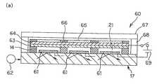
- FIGS. 8A and 8Bshow a light modulation element 60 in the fifth embodiment.
- FIG. 9is a plan view of a flat-panel display unit 100 .
- a plurality of first electrodes (signal electrodes) 61which are transparent and shaped like belts are formed in parallel with a predetermined spacing on a light guide plate 17 .
- Spacers 14each for separating the first adjacent electrodes 61 are formed on the light guide plate 17 .
- An ultraviolet lamp (low-pressure mercury lamp) 62 as a light sourceis disposed on the side of the light guide plate 17 and light from the low-pressure mercury lamp 62 is propagated while being totally reflected repeatedly in the light guide plate 17 .
- the spacer 14is formed on the upper end face with a transparent flexible thin film 63 at a position at a distance from the first electrode 61 . Therefore, a cavity 21 is formed between the first electrode 61 and the flexible thin film 63 .
- a plurality of second electrodes (scan electrodes) 64which are transparent and shaped like belts long in a direction orthogonal to the first electrodes 61 are formed in parallel in a predetermined spacing. That is, the first electrodes 61 and the second electrodes 64 are disposed like an orthogonal lattice, as shown in FIG. 9 .
- the first electrodes 61 and the second electrodes 64form matrix electrodes for enabling a specific counter electrode part to be specified by selecting a predetermined one.
- the second electrode 64is formed on the top with a fluorescent material 65 corresponding to the first electrode 61 .
- the fluorescent materials 65are placed in parallel to the first electrodes 61 and a black matrix 66 is formed between the adjacent fluorescent materials 65 for enhancing the contrast of a display image, as shown in FIG. 9 .
- a transparent front plate 67is placed on a support 68 above the fluorescent materials 65 with a predetermined spacing between the front panel and the fluorescent materials.
- a power supply 69is connected to the first electrodes 61 and the second electrodes 64 and from the power supply 69 , a voltage can be selectively applied to predetermined electrodes based on image information.
- the light modulation element 60not only a transparent glass plate, but also a resin film, etc., of polyethylene terephthalate, polycarbonate, etc., for example, can be used as a material of the light guide plate 17 .
- the first electrodes 61 and the second electrodes 64are formed of transparent conductive material, namely, metal or conductive metal compound generally put into fine particles and made transparent having an optical characteristic allowing ultraviolet rays to pass through.
- transparent conductive materialnamely, metal or conductive metal compound generally put into fine particles and made transparent having an optical characteristic allowing ultraviolet rays to pass through.
- Gold, silver, palladium, zinc, aluminum, etc.can be used as the metal, and indium oxide, zinc oxide, aluminum-added zinc oxide (popularly called AZO), etc., can be used as the metal compound.
- AZOaluminum-added zinc oxide
- an SnO 2 filmNesa film
- ITO filmetc.
- the light guide plate 17 , the first electrode 61 , the flexible thin film 63 , the second electrode 64 , and the fluorescent material 65make up a light modulation part 60 a.
- FIG. 8Bis a sectional view to show the operation state of the light modulation element shown in FIG. 8 A.
- the flexible thin film 63is attracted onto the first electrode 61 side and is bent by the electrostatic operation caused by an electrostatic force, whereby from the light guide plate 17 , light passes through the flexible thin film 63 for exciting the fluorescent material 65 to emit light, then the fluorescence is emitted. Therefore, voltage of the power supply 69 is selectively applied to the first electrodes 61 and the second electrodes 64 based on image information, whereby a desired image can be displayed.
- Such simple matrix drivecan cause the light modulation elements to well modulate light.
- the light modulation elementscan be easily put into an array by etching the light guide plates 17 , the first and second electrodes 61 and 64 , the spacers 14 , etc., the manufacturing costs can be reduced. Further, since light from the light guide plate 17 passes only through a pair of transparent electrodes with the cavity 21 between, the light is not absorbed fruitlessly and the light use efficiency can be enhanced.
- the light modulation elementmay be provided with a color filter for selecting a wavelength for any light path, an interference filter, a reflection film, etc., for enhancing the fluorescence emission efficiency.
- the space between the light guide plate 17 and the front plate 67 of the light modulation part 60 a formed in one piecemay be deaerated, then a rare gas may be poured for sealing the whole, thereby providing a flat-panel display unit intended for preventing the effect of disturbance for stabilization.
- FIG. 10is a plan view to show a light modulation element 70 of the sixth embodiment.
- FIG. 11is a sectional view taken on line C—C in FIG. 10 and
- FIG. 12is a sectional view taken on line D—D in FIG. 10 .
- FIG. 13is an equivalent circuit diagram of a pixel part shown in FIG. 10 .
- Simple matrix drivecan be applied to the light modulation elements 60 of the fifth embodiment described above; the light modulation elements 70 of the sixth embodiment are controlled by active drive.
- an active elementfor example, TFT
- the TFT 71is made up of a gate electrode 72 , an insulating film 73 , an a-Si:H layer 74 , one electrode (drain electrode) 75 , and one electrode (source electrode) 76 .
- the TFT 71is formed on a light guide plate 77 for guiding light from the end face thereof.
- a transparent pixel electrode 78is connected to the source electrode 76 of the TFT 71 .
- An image signal line 79 for each columnis connected to the drain electrode 75 .
- a scan signal line 80 for each rowis connected to the gate electrode 72 .
- the pixel electrode 78is deposited on a fluorescent material 81 a formed on the top of a flexible thin film 81 in the light modulation element 70 . Spacers 14 are bridged with the flexible thin film 81 .
- the light guide plate 77is formed with an opposite electrode (common electrode) 82 transparent for light from the light source, opposed to the pixel electrode 78 , and potential Vcom is applied.
- a voltage for bringing the TFT 71 into conductionis applied to the scan signal line 80 connected to the gate electrode 72 .
- a desired image signal voltageis applied to the image signal line 79 connected to the drain electrode 75 , the drain electrode 75 and the source electrode 76 are brought into conduction. Therefore, the image signal voltage is applied to the pixel electrode 78 , whereby an electrostatic force acts because of the voltage difference between the potential Vcom of the common electrode 82 and the potential of the pixel electrode 78 , causing the flexible thin film 81 to be bent to the light guide plate 77 side.
- desired light modulationcan be executed as in the embodiments described above.
- An optical filtermay be placed in a light path for enhancing the fluorescence emission efficiency or the pixel electrode 78 may be made a reflection electrode for enhancing the fluorescence emission efficiency.
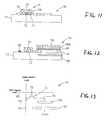
- one optical waveguideis made to correspond to one color and one pixel is displayed by means of a plurality of optical waveguides, as shown in FIG. 14 . That is, of light modulation elements arranged like a two-dimensional matrix, three light modulation elements 85 a , 85 b , and 85 c in total formed on a red (R) display optical waveguide 12 a , a green (G) display optical waveguide 12 b , and a blue (B) display optical waveguide 12 c adjacent to each other, for example, are made to correspond to a one-pixel area 86 . Fluorescent materials corresponding to display colors are placed on the optical waveguides. A black matrix 87 is formed between the adjacent optical waveguides for enhancing the contrast of a display image.
- LED, laser, EL, etc.can be named as a light source; particularly a light source for emitting ultraviolet rays is preferred.
- a combination of a discharge lamp and a light modulator, LED, laser, inorganic EL, organic EL, fluorescent display tube, FED, CRT, etc.can be named as the light source for emitting ultraviolet rays.
- a plurality of light modulation elements each corresponding to one pixelmay be provided for one optical waveguide and gradation drive may be executed with a plurality of light modulation elements of the same color, whereby if the light modulation elements are in a binary mode, multi-gradation drive in pixel units is enabled by performing drive control of the light modulation elements of the same color separately.
- the light modulation elements of the same colormay be divided into areas m 1 , m 2 , and m 3 different in area.
- the area ratio of the areas m 1 , m 2 , and m 3is 1:2:4 and light modulation elements 88 a , 88 b , and 88 c corresponding to the areas m 1 , m 2 , and m 3 are driven and controlled separately.
- the light modulation elements 88 a , 88 b , and 88 care provided for each color of R, G, and B of the three primary colors, for example, and are driven and controlled for each color.
- the passing-through light quantity as the whole of one pixelis made different by turning on and off the light modulation elements 88 a , 88 b , and 88 c in combination. Resultantly, if the binary state change of each light modulation part is made, eight levels of passing-through light quantity can be easily provided by using the binary state change of each light modulation part in combination.
- the light modulation element of the flat-panel display unitcomprises the light guide body for guiding light from the light source and the flexible thin film having the fluorescent material, wherein the distance between the flexible thin film and the light guide body is changed by the electromechanical operation and light emission of the fluorescent material excited by the guided light is controlled. Since the flexible thin film is thus provided with the fluorescent material, the excited fluorescent material emits scattered light, so that the viewing angle dependency is lessened and the viewability can be improved drastically. Since the fluorescent material can be excited directly by single-color light guided into the flexible thin film from the light guide body, the fluorescent material can be caused to emit light in high efficiency and fluorescence of any desired wavelength can be emitted with the light source at low costs.
- the fluorescent materialis placed directly on the flexible thin film, thus alignment of a flexible thin film substrate and a fluorescent material substrate required if the flexible thin film and the fluorescent material are provided as separate bodies on the different substrates becomes unnecessary, the structure becomes simple, and the manufacturing process can be simplified.
- the flexible thin film having the fluorescent materialis formed with the reflection film, whereby the light use efficiency can be enhanced easily.
- the light modulation elementcan be preferably applied to an exposure unit and a flat-panel display unit.
Landscapes
- Physics & Mathematics (AREA)
- General Physics & Mathematics (AREA)
- Optics & Photonics (AREA)
- Engineering & Computer Science (AREA)
- Spectroscopy & Molecular Physics (AREA)
- Computer Hardware Design (AREA)
- Theoretical Computer Science (AREA)
- Mechanical Light Control Or Optical Switches (AREA)
- Devices For Indicating Variable Information By Combining Individual Elements (AREA)
- Printers Or Recording Devices Using Electromagnetic And Radiation Means (AREA)
Abstract
Description
Claims (23)
Applications Claiming Priority (2)
| Application Number | Priority Date | Filing Date | Title |
|---|---|---|---|
| JP11-012031 | 1999-01-20 | ||
| JP1203199AJP2000214804A (en) | 1999-01-20 | 1999-01-20 | Light modulation element, aligner, and planar display |
Publications (1)
| Publication Number | Publication Date |
|---|---|
| US6642913B1true US6642913B1 (en) | 2003-11-04 |
Family
ID=11794250
Family Applications (1)
| Application Number | Title | Priority Date | Filing Date |
|---|---|---|---|
| US09/487,296Expired - Fee RelatedUS6642913B1 (en) | 1999-01-20 | 2000-01-19 | Light modulation element, exposure unit, and flat-panel display unit |
Country Status (2)
| Country | Link |
|---|---|
| US (1) | US6642913B1 (en) |
| JP (1) | JP2000214804A (en) |
Cited By (131)
| Publication number | Priority date | Publication date | Assignee | Title |
|---|---|---|---|---|
| US20020024483A1 (en)* | 2000-06-19 | 2002-02-28 | Takuya Makino | Optical switching element, and switching device and image display apparatus each using the optical switching element |
| US20030006978A1 (en)* | 2001-07-09 | 2003-01-09 | Tatsumi Fujiyoshi | Image-signal driving circuit eliminating the need to change order of inputting image data to source driver |
| US20040057101A1 (en)* | 2002-06-28 | 2004-03-25 | James Hunter | Reduced formation of asperities in contact micro-structures |
| US20040100201A1 (en)* | 2000-02-24 | 2004-05-27 | Van Gorkom Gerardus Gegorius Petrus | Display device comprising a light guide |
| US6753998B2 (en)* | 2001-03-30 | 2004-06-22 | Ngk Insulators, Ltd. | Optical system of display |
| US20040125281A1 (en)* | 2002-12-25 | 2004-07-01 | Wen-Jian Lin | Optical interference type of color display |
| US20040173806A1 (en)* | 2003-02-26 | 2004-09-09 | Chua Bee Yin Janet | Apparatus for producing a spectrally-shifted light output from a light emitting device utilizing thin-film luminescent layers |
| US20040203180A1 (en)* | 2000-10-17 | 2004-10-14 | Seiko Epson Corporation | Method of manufacture of active matrix substrate and liquid crystal display device |
| US20040222418A1 (en)* | 2003-01-17 | 2004-11-11 | Fuji Photo Film Co., Ltd. | Spatial light modulator, spatial light modulator array, image forming device and flat panel display |
| US6853476B2 (en)* | 2003-04-30 | 2005-02-08 | Hewlett-Packard Development Company, L.P. | Charge control circuit for a micro-electromechanical device |
| US20050078348A1 (en)* | 2003-09-30 | 2005-04-14 | Wen-Jian Lin | Structure of a micro electro mechanical system and the manufacturing method thereof |
| US20050123243A1 (en)* | 2003-12-08 | 2005-06-09 | The University Of Cincinnati | Light emissive display based on lightwave coupling |
| GB2409515A (en)* | 2003-12-24 | 2005-06-29 | Nokia Corp | Analogue navigation device utilising differing refractive indices |
| US20050163411A1 (en)* | 2000-11-15 | 2005-07-28 | Fuji Photo Film Co., Ltd. | Optical modulator, exposure head and image recording apparatus |
| WO2005071461A1 (en)* | 2004-01-21 | 2005-08-04 | Koninklijke Philips Electronics N.V. | Display device |
| US20050168849A1 (en)* | 2003-04-21 | 2005-08-04 | Prime View International Co., Ltd. | Method for fabricating an interference display unit |
| US20050174507A1 (en)* | 2002-05-21 | 2005-08-11 | Koninklijke Philips Electronics N.V. | Display panel comprising a light guide plate |
| US20050202649A1 (en)* | 2004-03-10 | 2005-09-15 | Po-Chung Hung | Optical interference reflective element and repairing and manufacturing methods thereof |
| US20060001786A1 (en)* | 2002-08-14 | 2006-01-05 | Koninklijke Philips Electronics N.V. | Display device comprising a light guide |
| US20060034566A1 (en)* | 2002-11-05 | 2006-02-16 | Matsushita Electric Industrial Co., Ltd. | Display element and display using the same |
| US20060077519A1 (en)* | 2004-09-27 | 2006-04-13 | Floyd Philip D | System and method for providing thermal compensation for an interferometric modulator display |
| US20060119922A1 (en)* | 2004-12-07 | 2006-06-08 | Faase Kenneth J | Light modulator device |
| US20060148121A1 (en)* | 2005-01-03 | 2006-07-06 | Miradia Inc. | Method and structure for forming an integrated spatial light modulator |
| US20060182389A1 (en)* | 2002-03-26 | 2006-08-17 | Duine Peter A | Display device comprising a light transmitting first plate and light-absorbing means |
| US20060209000A1 (en)* | 2001-10-23 | 2006-09-21 | Ken Sumiyoshi | Liquid crystal display device, backlight used for same display device, method for driving same backlight and method for manufacturing same backlight |
| US20060256420A1 (en)* | 2003-06-24 | 2006-11-16 | Miles Mark W | Film stack for manufacturing micro-electromechanical systems (MEMS) devices |
| US20060257070A1 (en)* | 2003-05-26 | 2006-11-16 | Wen-Jian Lin | Optical interference display cell and method of making the same |
| US20070031097A1 (en)* | 2003-12-08 | 2007-02-08 | University Of Cincinnati | Light Emissive Signage Devices Based on Lightwave Coupling |
| US7250315B2 (en) | 2002-02-12 | 2007-07-31 | Idc, Llc | Method for fabricating a structure for a microelectromechanical system (MEMS) device |
| EP1418457A4 (en)* | 2001-07-19 | 2007-08-01 | Fujifilm Corp | Optical modulating device, display, and exposure device |
| US20070236774A1 (en)* | 2006-04-10 | 2007-10-11 | Evgeni Gousev | Interferometric optical display system with broadband characteristics |
| US20070247696A1 (en)* | 2006-04-19 | 2007-10-25 | Teruo Sasagawa | Microelectromechanical device and method utilizing a porous surface |
| US7297471B1 (en) | 2003-04-15 | 2007-11-20 | Idc, Llc | Method for manufacturing an array of interferometric modulators |
| US20070279944A1 (en)* | 2006-06-05 | 2007-12-06 | Epson Imaging Devices Corporation | Illumination device, liquid crystal device, and electronic apparatus |
| US20070279730A1 (en)* | 2006-06-01 | 2007-12-06 | David Heald | Process and structure for fabrication of mems device having isolated egde posts |
| US20070297191A1 (en)* | 2006-06-21 | 2007-12-27 | Sampsell Jeffrey B | Linear solid state illuminator |
| US7349139B2 (en) | 2004-09-27 | 2008-03-25 | Idc, Llc | System and method of illuminating interferometric modulators using backlighting |
| US7349136B2 (en) | 2004-09-27 | 2008-03-25 | Idc, Llc | Method and device for a display having transparent components integrated therein |
| US7369292B2 (en) | 2006-05-03 | 2008-05-06 | Qualcomm Mems Technologies, Inc. | Electrode and interconnect materials for MEMS devices |
| US7369296B2 (en) | 2004-09-27 | 2008-05-06 | Idc, Llc | Device and method for modifying actuation voltage thresholds of a deformable membrane in an interferometric modulator |
| US7373026B2 (en) | 2004-09-27 | 2008-05-13 | Idc, Llc | MEMS device fabricated on a pre-patterned substrate |
| US7382515B2 (en) | 2006-01-18 | 2008-06-03 | Qualcomm Mems Technologies, Inc. | Silicon-rich silicon nitrides as etch stops in MEMS manufacture |
| US7405861B2 (en) | 2004-09-27 | 2008-07-29 | Idc, Llc | Method and device for protecting interferometric modulators from electrostatic discharge |
| US7405863B2 (en) | 2006-06-01 | 2008-07-29 | Qualcomm Mems Technologies, Inc. | Patterning of mechanical layer in MEMS to reduce stresses at supports |
| US20080196814A1 (en)* | 2005-10-13 | 2008-08-21 | Miradia Inc. | Spatial light modulator with multi-layer landing structures |
| US7417783B2 (en) | 2004-09-27 | 2008-08-26 | Idc, Llc | Mirror and mirror layer for optical modulator and method |
| US7420728B2 (en) | 2004-09-27 | 2008-09-02 | Idc, Llc | Methods of fabricating interferometric modulators by selectively removing a material |
| US7450295B2 (en) | 2006-03-02 | 2008-11-11 | Qualcomm Mems Technologies, Inc. | Methods for producing MEMS with protective coatings using multi-component sacrificial layers |
| US7485236B2 (en) | 2003-08-26 | 2009-02-03 | Qualcomm Mems Technologies, Inc. | Interference display cell and fabrication method thereof |
| US7486854B2 (en) | 2006-01-24 | 2009-02-03 | Uni-Pixel Displays, Inc. | Optical microstructures for light extraction and control |
| US7486867B2 (en) | 2005-08-19 | 2009-02-03 | Qualcomm Mems Technologies, Inc. | Methods for forming layers within a MEMS device using liftoff processes to achieve a tapered edge |
| US7492502B2 (en) | 2004-09-27 | 2009-02-17 | Idc, Llc | Method of fabricating a free-standing microstructure |
| US7527996B2 (en) | 2006-04-19 | 2009-05-05 | Qualcomm Mems Technologies, Inc. | Non-planar surface structures and process for microelectromechanical systems |
| US7535621B2 (en) | 2006-12-27 | 2009-05-19 | Qualcomm Mems Technologies, Inc. | Aluminum fluoride films for microelectromechanical system applications |
| US7534640B2 (en) | 2005-07-22 | 2009-05-19 | Qualcomm Mems Technologies, Inc. | Support structure for MEMS device and methods therefor |
| US7545552B2 (en) | 2006-10-19 | 2009-06-09 | Qualcomm Mems Technologies, Inc. | Sacrificial spacer process and resultant structure for MEMS support structure |
| US7547568B2 (en) | 2006-02-22 | 2009-06-16 | Qualcomm Mems Technologies, Inc. | Electrical conditioning of MEMS device and insulating layer thereof |
| US7547565B2 (en) | 2005-02-04 | 2009-06-16 | Qualcomm Mems Technologies, Inc. | Method of manufacturing optical interference color display |
| US7550794B2 (en) | 2002-09-20 | 2009-06-23 | Idc, Llc | Micromechanical systems device comprising a displaceable electrode and a charge-trapping layer |
| US7553684B2 (en) | 2004-09-27 | 2009-06-30 | Idc, Llc | Method of fabricating interferometric devices using lift-off processing techniques |
| US7566664B2 (en) | 2006-08-02 | 2009-07-28 | Qualcomm Mems Technologies, Inc. | Selective etching of MEMS using gaseous halides and reactive co-etchants |
| US7566940B2 (en) | 2005-07-22 | 2009-07-28 | Qualcomm Mems Technologies, Inc. | Electromechanical devices having overlying support structures |
| US7603001B2 (en) | 2006-02-17 | 2009-10-13 | Qualcomm Mems Technologies, Inc. | Method and apparatus for providing back-lighting in an interferometric modulator display device |
| US20090256823A1 (en)* | 2005-12-02 | 2009-10-15 | Tokyo, The University Of | Display Device and Transparent Magnetic Film |
| US20090257108A1 (en)* | 2008-04-15 | 2009-10-15 | Qualcomm Mems Technologies, Inc. | Light with bi-directional propagation |
| US7623287B2 (en) | 2006-04-19 | 2009-11-24 | Qualcomm Mems Technologies, Inc. | Non-planar surface structures and process for microelectromechanical systems |
| US7625825B2 (en) | 2007-06-14 | 2009-12-01 | Qualcomm Mems Technologies, Inc. | Method of patterning mechanical layer for MEMS structures |
| US7630123B2 (en) | 2004-09-27 | 2009-12-08 | Qualcomm Mems Technologies, Inc. | Method and device for compensating for color shift as a function of angle of view |
| US7630114B2 (en) | 2005-10-28 | 2009-12-08 | Idc, Llc | Diffusion barrier layer for MEMS devices |
| EP1554626A4 (en)* | 2002-07-02 | 2010-01-20 | Idc Llc | A device having a light-absorbing mask and a method for fabricating same |
| US7684104B2 (en) | 2004-09-27 | 2010-03-23 | Idc, Llc | MEMS using filler material and method |
| US7697052B1 (en) | 1999-02-17 | 2010-04-13 | Semiconductor Energy Laboratory Co., Ltd. | Electronic view finder utilizing an organic electroluminescence display |
| US7706050B2 (en) | 2004-03-05 | 2010-04-27 | Qualcomm Mems Technologies, Inc. | Integrated modulator illumination |
| US7706042B2 (en) | 2006-12-20 | 2010-04-27 | Qualcomm Mems Technologies, Inc. | MEMS device and interconnects for same |
| US7711239B2 (en) | 2006-04-19 | 2010-05-04 | Qualcomm Mems Technologies, Inc. | Microelectromechanical device and method utilizing nanoparticles |
| US7710636B2 (en) | 2004-09-27 | 2010-05-04 | Qualcomm Mems Technologies, Inc. | Systems and methods using interferometric optical modulators and diffusers |
| US7710632B2 (en) | 2004-09-27 | 2010-05-04 | Qualcomm Mems Technologies, Inc. | Display device having an array of spatial light modulators with integrated color filters |
| US20100109102A1 (en)* | 2005-01-03 | 2010-05-06 | Miradia Inc. | Method and structure for forming a gyroscope and accelerometer |
| US7719747B2 (en) | 2004-09-27 | 2010-05-18 | Qualcomm Mems Technologies, Inc. | Method and post structures for interferometric modulation |
| US7719752B2 (en) | 2007-05-11 | 2010-05-18 | Qualcomm Mems Technologies, Inc. | MEMS structures, methods of fabricating MEMS components on separate substrates and assembly of same |
| US7733439B2 (en) | 2007-04-30 | 2010-06-08 | Qualcomm Mems Technologies, Inc. | Dual film light guide for illuminating displays |
| US7750886B2 (en) | 2004-09-27 | 2010-07-06 | Qualcomm Mems Technologies, Inc. | Methods and devices for lighting displays |
| US7763546B2 (en) | 2006-08-02 | 2010-07-27 | Qualcomm Mems Technologies, Inc. | Methods for reducing surface charges during the manufacture of microelectromechanical systems devices |
| US7777954B2 (en) | 2007-01-30 | 2010-08-17 | Qualcomm Mems Technologies, Inc. | Systems and methods of providing a light guiding layer |
| US7781850B2 (en) | 2002-09-20 | 2010-08-24 | Qualcomm Mems Technologies, Inc. | Controlling electromechanical behavior of structures within a microelectromechanical systems device |
| US7795061B2 (en) | 2005-12-29 | 2010-09-14 | Qualcomm Mems Technologies, Inc. | Method of creating MEMS device cavities by a non-etching process |
| US7807488B2 (en) | 2004-09-27 | 2010-10-05 | Qualcomm Mems Technologies, Inc. | Display element having filter material diffused in a substrate of the display element |
| US7813026B2 (en) | 2004-09-27 | 2010-10-12 | Qualcomm Mems Technologies, Inc. | System and method of reducing color shift in a display |
| US7845841B2 (en) | 2006-08-28 | 2010-12-07 | Qualcomm Mems Technologies, Inc. | Angle sweeping holographic illuminator |
| US7855827B2 (en) | 2006-10-06 | 2010-12-21 | Qualcomm Mems Technologies, Inc. | Internal optical isolation structure for integrated front or back lighting |
| US7863079B2 (en) | 2008-02-05 | 2011-01-04 | Qualcomm Mems Technologies, Inc. | Methods of reducing CD loss in a microelectromechanical device |
| US7864395B2 (en) | 2006-10-27 | 2011-01-04 | Qualcomm Mems Technologies, Inc. | Light guide including optical scattering elements and a method of manufacture |
| US20110007377A1 (en)* | 2007-12-14 | 2011-01-13 | Rambus Inc | Apparatus and method for reducing pixel operational voltage in mems-based optical displays |
| US7911428B2 (en) | 2004-09-27 | 2011-03-22 | Qualcomm Mems Technologies, Inc. | Method and device for manipulating color in a display |
| US7916980B2 (en)* | 2006-01-13 | 2011-03-29 | Qualcomm Mems Technologies, Inc. | Interconnect structure for MEMS device |
| US20110090157A1 (en)* | 2009-10-15 | 2011-04-21 | Inventec Appliances (Shanghai) Co. Ltd. | Touch Display Apparatus and Manufacturing Method Thereof |
| US7949213B2 (en) | 2007-12-07 | 2011-05-24 | Qualcomm Mems Technologies, Inc. | Light illumination of displays with front light guide and coupling elements |
| US7986451B2 (en) | 2004-09-27 | 2011-07-26 | Qualcomm Mems Technologies, Inc. | Optical films for directing light towards active areas of displays |
| US8040589B2 (en) | 2008-02-12 | 2011-10-18 | Qualcomm Mems Technologies, Inc. | Devices and methods for enhancing brightness of displays using angle conversion layers |
| US8045252B2 (en) | 2004-02-03 | 2011-10-25 | Qualcomm Mems Technologies, Inc. | Spatial light modulator with integrated optical compensation structure |
| US8061882B2 (en) | 2006-10-06 | 2011-11-22 | Qualcomm Mems Technologies, Inc. | Illumination device with built-in light coupler |
| US8068268B2 (en) | 2007-07-03 | 2011-11-29 | Qualcomm Mems Technologies, Inc. | MEMS devices having improved uniformity and methods for making them |
| US8068710B2 (en) | 2007-12-07 | 2011-11-29 | Qualcomm Mems Technologies, Inc. | Decoupled holographic film and diffuser |
| US8107155B2 (en) | 2006-10-06 | 2012-01-31 | Qualcomm Mems Technologies, Inc. | System and method for reducing visual artifacts in displays |
| US8111446B2 (en) | 2004-09-27 | 2012-02-07 | Qualcomm Mems Technologies, Inc. | Optical films for controlling angular characteristics of displays |
| WO2012047760A1 (en)* | 2010-10-05 | 2012-04-12 | Qualcomm Mems Technologies, Inc. | Method for eliminating row or column routing on array periphery |
| US8172417B2 (en) | 2009-03-06 | 2012-05-08 | Qualcomm Mems Technologies, Inc. | Shaped frontlight reflector for use with display |
| US8231257B2 (en) | 2009-01-13 | 2012-07-31 | Qualcomm Mems Technologies, Inc. | Large area light panel and screen |
| US20120250347A1 (en)* | 2011-04-04 | 2012-10-04 | Hyun-Min Cho | Backlight assembly, method of manufacturing the same and display apparatus having the same |
| US8300304B2 (en) | 2008-02-12 | 2012-10-30 | Qualcomm Mems Technologies, Inc. | Integrated front light diffuser for reflective displays |
| WO2012148847A1 (en)* | 2011-04-26 | 2012-11-01 | Qualcomm Mems Technologies, Inc. | Thin film transistors (tft) active-matrix imod pixel layout |
| US8346048B2 (en) | 2008-05-28 | 2013-01-01 | Qualcomm Mems Technologies, Inc. | Front light devices and methods of fabrication thereof |
| US8368981B2 (en) | 2006-10-10 | 2013-02-05 | Qualcomm Mems Technologies, Inc. | Display device with diffractive optics |
| US8402647B2 (en) | 2010-08-25 | 2013-03-26 | Qualcomm Mems Technologies Inc. | Methods of manufacturing illumination systems |
| US8638491B2 (en) | 2004-09-27 | 2014-01-28 | Qualcomm Mems Technologies, Inc. | Device having a conductive light absorbing mask and method for fabricating same |
| US8654061B2 (en) | 2008-02-12 | 2014-02-18 | Qualcomm Mems Technologies, Inc. | Integrated front light solution |
| US8659816B2 (en) | 2011-04-25 | 2014-02-25 | Qualcomm Mems Technologies, Inc. | Mechanical layer and methods of making the same |
| US8848294B2 (en) | 2010-05-20 | 2014-09-30 | Qualcomm Mems Technologies, Inc. | Method and structure capable of changing color saturation |
| US8872085B2 (en) | 2006-10-06 | 2014-10-28 | Qualcomm Mems Technologies, Inc. | Display device having front illuminator with turning features |
| US8902484B2 (en) | 2010-12-15 | 2014-12-02 | Qualcomm Mems Technologies, Inc. | Holographic brightness enhancement film |
| US8928967B2 (en) | 1998-04-08 | 2015-01-06 | Qualcomm Mems Technologies, Inc. | Method and device for modulating light |
| US8979349B2 (en) | 2009-05-29 | 2015-03-17 | Qualcomm Mems Technologies, Inc. | Illumination devices and methods of fabrication thereof |
| US9019183B2 (en) | 2006-10-06 | 2015-04-28 | Qualcomm Mems Technologies, Inc. | Optical loss structure integrated in an illumination apparatus |
| US9086564B2 (en) | 2004-09-27 | 2015-07-21 | Qualcomm Mems Technologies, Inc. | Conductive bus structure for interferometric modulator array |
| US9110289B2 (en) | 1998-04-08 | 2015-08-18 | Qualcomm Mems Technologies, Inc. | Device for modulating light with multiple electrodes |
| KR20170027505A (en)* | 2015-09-02 | 2017-03-10 | 삼성전자주식회사 | Backlight unit using micro optical switch, and display apparatus having the same |
| WO2018236535A1 (en)* | 2017-06-21 | 2018-12-27 | Microsoft Technology Licensing, Llc | DISPLAY SYSTEM DRIVER |
| US10309615B2 (en) | 2015-02-09 | 2019-06-04 | Sun Chemical Corporation | Light emissive display based on lightwave coupling in combination with visible light illuminated content |
| US20190369442A1 (en)* | 2018-05-31 | 2019-12-05 | Wuhan China Star Optoelectronics Technology Co., Ltd. | Backlight module and display device |
| US10816851B2 (en) | 2019-01-30 | 2020-10-27 | Dell Products L.P. | Thin information handling system display light guide plate spacing |
| CN114690314A (en)* | 2020-12-28 | 2022-07-01 | 中芯国际集成电路制造(上海)有限公司 | Semiconductor structure and forming method thereof |
Families Citing this family (10)
| Publication number | Priority date | Publication date | Assignee | Title |
|---|---|---|---|---|
| JP2002341268A (en)* | 2001-05-11 | 2002-11-27 | Sony Corp | Display device |
| KR101088329B1 (en) | 2003-01-16 | 2011-11-30 | 스미또모 가가꾸 가부시끼가이샤 | Anti-glare film, its manufacturing method and display device equipped with anti-glare film |
| GB0406540D0 (en)* | 2004-03-24 | 2004-04-28 | Koninkl Philips Electronics Nv | Electroluminescent display devices |
| US7345805B2 (en) | 2004-09-27 | 2008-03-18 | Idc, Llc | Interferometric modulator array with integrated MEMS electrical switches |
| JP4559838B2 (en)* | 2004-12-13 | 2010-10-13 | 株式会社サムスン横浜研究所 | Optical recording head and image forming apparatus |
| JP2006350140A (en)* | 2005-06-20 | 2006-12-28 | Nikon Corp | Display device and resist used therefor |
| JP4887755B2 (en)* | 2005-11-22 | 2012-02-29 | ソニー株式会社 | Electrostatic drive element and projector using the same |
| JP5344616B2 (en)* | 2009-11-18 | 2013-11-20 | キヤノン株式会社 | Electrophotographic image forming apparatus |
| JP5666945B2 (en)* | 2011-02-28 | 2015-02-12 | 株式会社東芝 | Display element and display device |
| JP6001842B2 (en)* | 2011-11-15 | 2016-10-05 | 株式会社東芝 | Display device |
Citations (8)
| Publication number | Priority date | Publication date | Assignee | Title |
|---|---|---|---|---|
| US5858564A (en)* | 1996-12-27 | 1999-01-12 | Sony Corporation | Organic electroluminescent devices and luminescent display employing such organic electroluminescent devices |
| US5914760A (en)* | 1996-06-21 | 1999-06-22 | Casio Computer Co., Ltd. | Surface light source device and liquid crystal display device using the same |
| US5965064A (en)* | 1997-10-28 | 1999-10-12 | Sony Chemicals Corporation | Anisotropically electroconductive adhesive and adhesive film |
| US6195196B1 (en)* | 1998-03-13 | 2001-02-27 | Fuji Photo Film Co., Ltd. | Array-type exposing device and flat type display incorporating light modulator and driving method thereof |
| US6288829B1 (en)* | 1998-10-05 | 2001-09-11 | Fuji Photo Film, Co., Ltd. | Light modulation element, array-type light modulation element, and flat-panel display unit |
| US6327071B1 (en)* | 1998-10-16 | 2001-12-04 | Fuji Photo Film Co., Ltd. | Drive methods of array-type light modulation element and flat-panel display |
| US6338910B1 (en)* | 1998-09-11 | 2002-01-15 | Sony Corporation | Organic electroluminescent device |
| US6344156B1 (en)* | 1998-12-25 | 2002-02-05 | Sony Chemicals Corporation | Anisotropic conductive adhesive film |
- 1999
- 1999-01-20JPJP1203199Apatent/JP2000214804A/enactivePending
- 2000
- 2000-01-19USUS09/487,296patent/US6642913B1/ennot_activeExpired - Fee Related
Patent Citations (8)
| Publication number | Priority date | Publication date | Assignee | Title |
|---|---|---|---|---|
| US5914760A (en)* | 1996-06-21 | 1999-06-22 | Casio Computer Co., Ltd. | Surface light source device and liquid crystal display device using the same |
| US5858564A (en)* | 1996-12-27 | 1999-01-12 | Sony Corporation | Organic electroluminescent devices and luminescent display employing such organic electroluminescent devices |
| US5965064A (en)* | 1997-10-28 | 1999-10-12 | Sony Chemicals Corporation | Anisotropically electroconductive adhesive and adhesive film |
| US6195196B1 (en)* | 1998-03-13 | 2001-02-27 | Fuji Photo Film Co., Ltd. | Array-type exposing device and flat type display incorporating light modulator and driving method thereof |
| US6338910B1 (en)* | 1998-09-11 | 2002-01-15 | Sony Corporation | Organic electroluminescent device |
| US6288829B1 (en)* | 1998-10-05 | 2001-09-11 | Fuji Photo Film, Co., Ltd. | Light modulation element, array-type light modulation element, and flat-panel display unit |
| US6327071B1 (en)* | 1998-10-16 | 2001-12-04 | Fuji Photo Film Co., Ltd. | Drive methods of array-type light modulation element and flat-panel display |
| US6344156B1 (en)* | 1998-12-25 | 2002-02-05 | Sony Chemicals Corporation | Anisotropic conductive adhesive film |
Cited By (205)
| Publication number | Priority date | Publication date | Assignee | Title |
|---|---|---|---|---|
| US9110289B2 (en) | 1998-04-08 | 2015-08-18 | Qualcomm Mems Technologies, Inc. | Device for modulating light with multiple electrodes |
| US8928967B2 (en) | 1998-04-08 | 2015-01-06 | Qualcomm Mems Technologies, Inc. | Method and device for modulating light |
| US7697052B1 (en) | 1999-02-17 | 2010-04-13 | Semiconductor Energy Laboratory Co., Ltd. | Electronic view finder utilizing an organic electroluminescence display |
| US20040100201A1 (en)* | 2000-02-24 | 2004-05-27 | Van Gorkom Gerardus Gegorius Petrus | Display device comprising a light guide |
| US6956332B2 (en)* | 2000-02-24 | 2005-10-18 | Koninklijke Philips Electronics N.V. | Display device comprising a light guide |
| US7061455B2 (en)* | 2000-06-19 | 2006-06-13 | Sony Corporation | Optical switching element, and switching device and image display apparatus each using the optical switching element |
| US20050179681A1 (en)* | 2000-06-19 | 2005-08-18 | Sony Corp. | Optical switching element, and switching device and image display apparatus each using the optical switching element |
| US7199772B2 (en)* | 2000-06-19 | 2007-04-03 | Sony Corporation | Optical switching element, and switching device and image display apparatus each using the optical switching element |
| US20020024483A1 (en)* | 2000-06-19 | 2002-02-28 | Takuya Makino | Optical switching element, and switching device and image display apparatus each using the optical switching element |
| US6917352B2 (en)* | 2000-06-19 | 2005-07-12 | Sony Corporation | Optical switching element, and switching device and image display apparatus each using the optical switching element |
| US20050179680A1 (en)* | 2000-06-19 | 2005-08-18 | Sony Corp. | Optical switching element, and switching device and image display apparatus each using the optical switching element |
| US20040203180A1 (en)* | 2000-10-17 | 2004-10-14 | Seiko Epson Corporation | Method of manufacture of active matrix substrate and liquid crystal display device |
| US7037737B2 (en)* | 2000-10-17 | 2006-05-02 | Seiko Epson Corporation | Method of manufacture of active matrix substrate and liquid crystal display device |
| US20050163411A1 (en)* | 2000-11-15 | 2005-07-28 | Fuji Photo Film Co., Ltd. | Optical modulator, exposure head and image recording apparatus |
| US6753998B2 (en)* | 2001-03-30 | 2004-06-22 | Ngk Insulators, Ltd. | Optical system of display |
| US20030006978A1 (en)* | 2001-07-09 | 2003-01-09 | Tatsumi Fujiyoshi | Image-signal driving circuit eliminating the need to change order of inputting image data to source driver |
| US6922189B2 (en)* | 2001-07-09 | 2005-07-26 | Alps Electric Co., Ltd. | Image-signal driving circuit eliminating the need to change order of inputting image data to source driver |
| EP1418457A4 (en)* | 2001-07-19 | 2007-08-01 | Fujifilm Corp | Optical modulating device, display, and exposure device |
| US9111495B2 (en) | 2001-10-23 | 2015-08-18 | Getner Foundation Llc | Liquid crystal display device, backlight used for same display device, method for driving same backlight and method for manufacturing same backlight |
| US8599125B2 (en) | 2001-10-23 | 2013-12-03 | Getner Foundation Llc | Liquid crystal display device, backlight used for same display device, method for driving same backlight and method for manufacturing same backlight |
| US20090251641A1 (en)* | 2001-10-23 | 2009-10-08 | Ken Sumiyoshi | Liquid crystal display device, backlight used for same display device, method for driving same backlight and method for manufacturing same backlight |
| US7598939B2 (en)* | 2001-10-23 | 2009-10-06 | Nec Corporation | Liquid crystal display device, backlight used for same display device, method for driving same backlight and method for manufacturing same backlight |
| US20060209000A1 (en)* | 2001-10-23 | 2006-09-21 | Ken Sumiyoshi | Liquid crystal display device, backlight used for same display device, method for driving same backlight and method for manufacturing same backlight |
| US7642110B2 (en) | 2002-02-12 | 2010-01-05 | Qualcomm Mems Technologies, Inc. | Method for fabricating a structure for a microelectromechanical systems (MEMS) device |
| US7250315B2 (en) | 2002-02-12 | 2007-07-31 | Idc, Llc | Method for fabricating a structure for a microelectromechanical system (MEMS) device |
| US20060182389A1 (en)* | 2002-03-26 | 2006-08-17 | Duine Peter A | Display device comprising a light transmitting first plate and light-absorbing means |
| US7370987B2 (en)* | 2002-05-21 | 2008-05-13 | Koninklijke Philips Electronics N.V. | Display panel comprising a light guide plate |
| US20050174507A1 (en)* | 2002-05-21 | 2005-08-11 | Koninklijke Philips Electronics N.V. | Display panel comprising a light guide plate |
| US20040057101A1 (en)* | 2002-06-28 | 2004-03-25 | James Hunter | Reduced formation of asperities in contact micro-structures |
| US6813059B2 (en)* | 2002-06-28 | 2004-11-02 | Silicon Light Machines, Inc. | Reduced formation of asperities in contact micro-structures |
| EP1554626A4 (en)* | 2002-07-02 | 2010-01-20 | Idc Llc | A device having a light-absorbing mask and a method for fabricating same |
| US20060001786A1 (en)* | 2002-08-14 | 2006-01-05 | Koninklijke Philips Electronics N.V. | Display device comprising a light guide |
| US7781850B2 (en) | 2002-09-20 | 2010-08-24 | Qualcomm Mems Technologies, Inc. | Controlling electromechanical behavior of structures within a microelectromechanical systems device |
| US7550794B2 (en) | 2002-09-20 | 2009-06-23 | Idc, Llc | Micromechanical systems device comprising a displaceable electrode and a charge-trapping layer |
| US7236663B2 (en)* | 2002-11-05 | 2007-06-26 | Matsushita Electric Industrial Co., Ltd. | Display element and display device using the same |
| US20060034566A1 (en)* | 2002-11-05 | 2006-02-16 | Matsushita Electric Industrial Co., Ltd. | Display element and display using the same |
| US20040125281A1 (en)* | 2002-12-25 | 2004-07-01 | Wen-Jian Lin | Optical interference type of color display |
| US9025235B2 (en) | 2002-12-25 | 2015-05-05 | Qualcomm Mems Technologies, Inc. | Optical interference type of color display having optical diffusion layer between substrate and electrode |
| US7342709B2 (en)* | 2002-12-25 | 2008-03-11 | Qualcomm Mems Technologies, Inc. | Optical interference type of color display having optical diffusion layer between substrate and electrode |
| US20040222418A1 (en)* | 2003-01-17 | 2004-11-11 | Fuji Photo Film Co., Ltd. | Spatial light modulator, spatial light modulator array, image forming device and flat panel display |
| US6930816B2 (en)* | 2003-01-17 | 2005-08-16 | Fuji Photo Film Co., Ltd. | Spatial light modulator, spatial light modulator array, image forming device and flat panel display |
| US20040173806A1 (en)* | 2003-02-26 | 2004-09-09 | Chua Bee Yin Janet | Apparatus for producing a spectrally-shifted light output from a light emitting device utilizing thin-film luminescent layers |
| US7423296B2 (en)* | 2003-02-26 | 2008-09-09 | Avago Technologies Ecbu Ip Pte Ltd | Apparatus for producing a spectrally-shifted light output from a light emitting device utilizing thin-film luminescent layers |
| US7297471B1 (en) | 2003-04-15 | 2007-11-20 | Idc, Llc | Method for manufacturing an array of interferometric modulators |
| US20050168849A1 (en)* | 2003-04-21 | 2005-08-04 | Prime View International Co., Ltd. | Method for fabricating an interference display unit |
| US7016095B2 (en)* | 2003-04-21 | 2006-03-21 | Prime View International Co., Ltd. | Method for fabricating an interference display unit |
| US6853476B2 (en)* | 2003-04-30 | 2005-02-08 | Hewlett-Packard Development Company, L.P. | Charge control circuit for a micro-electromechanical device |
| US20060257070A1 (en)* | 2003-05-26 | 2006-11-16 | Wen-Jian Lin | Optical interference display cell and method of making the same |
| US7706044B2 (en) | 2003-05-26 | 2010-04-27 | Qualcomm Mems Technologies, Inc. | Optical interference display cell and method of making the same |
| US20060256420A1 (en)* | 2003-06-24 | 2006-11-16 | Miles Mark W | Film stack for manufacturing micro-electromechanical systems (MEMS) devices |
| US7616369B2 (en) | 2003-06-24 | 2009-11-10 | Idc, Llc | Film stack for manufacturing micro-electromechanical systems (MEMS) devices |
| US7485236B2 (en) | 2003-08-26 | 2009-02-03 | Qualcomm Mems Technologies, Inc. | Interference display cell and fabrication method thereof |
| US20050078348A1 (en)* | 2003-09-30 | 2005-04-14 | Wen-Jian Lin | Structure of a micro electro mechanical system and the manufacturing method thereof |
| US7291921B2 (en) | 2003-09-30 | 2007-11-06 | Qualcomm Mems Technologies, Inc. | Structure of a micro electro mechanical system and the manufacturing method thereof |
| US7123796B2 (en) | 2003-12-08 | 2006-10-17 | University Of Cincinnati | Light emissive display based on lightwave coupling |
| WO2005057261A3 (en)* | 2003-12-08 | 2005-10-06 | Univ Cincinnati | Light emissive display based on lightwave coupling |
| US20070031097A1 (en)* | 2003-12-08 | 2007-02-08 | University Of Cincinnati | Light Emissive Signage Devices Based on Lightwave Coupling |
| US7430355B2 (en) | 2003-12-08 | 2008-09-30 | University Of Cincinnati | Light emissive signage devices based on lightwave coupling |
| US20050123243A1 (en)* | 2003-12-08 | 2005-06-09 | The University Of Cincinnati | Light emissive display based on lightwave coupling |
| CN100470456C (en)* | 2003-12-24 | 2009-03-18 | 诺基亚公司 | Analog navigation device, handheld electronic device, navigation method and key control device |
| GB2409515A (en)* | 2003-12-24 | 2005-06-29 | Nokia Corp | Analogue navigation device utilising differing refractive indices |
| US20070147731A1 (en)* | 2003-12-24 | 2007-06-28 | Philip Barrowclough | Analogue navigation device |
| WO2005071461A1 (en)* | 2004-01-21 | 2005-08-04 | Koninklijke Philips Electronics N.V. | Display device |
| US9019590B2 (en) | 2004-02-03 | 2015-04-28 | Qualcomm Mems Technologies, Inc. | Spatial light modulator with integrated optical compensation structure |
| US8045252B2 (en) | 2004-02-03 | 2011-10-25 | Qualcomm Mems Technologies, Inc. | Spatial light modulator with integrated optical compensation structure |
| US8111445B2 (en) | 2004-02-03 | 2012-02-07 | Qualcomm Mems Technologies, Inc. | Spatial light modulator with integrated optical compensation structure |
| US7880954B2 (en) | 2004-03-05 | 2011-02-01 | Qualcomm Mems Technologies, Inc. | Integrated modulator illumination |
| US7706050B2 (en) | 2004-03-05 | 2010-04-27 | Qualcomm Mems Technologies, Inc. | Integrated modulator illumination |
| US20050202649A1 (en)* | 2004-03-10 | 2005-09-15 | Po-Chung Hung | Optical interference reflective element and repairing and manufacturing methods thereof |
| US6980350B2 (en)* | 2004-03-10 | 2005-12-27 | Prime View International Co., Ltd. | Optical interference reflective element and repairing and manufacturing methods thereof |
| US7349139B2 (en) | 2004-09-27 | 2008-03-25 | Idc, Llc | System and method of illuminating interferometric modulators using backlighting |
| US7349136B2 (en) | 2004-09-27 | 2008-03-25 | Idc, Llc | Method and device for a display having transparent components integrated therein |
| US7417783B2 (en) | 2004-09-27 | 2008-08-26 | Idc, Llc | Mirror and mirror layer for optical modulator and method |
| US7429334B2 (en) | 2004-09-27 | 2008-09-30 | Idc, Llc | Methods of fabricating interferometric modulators by selectively removing a material |
| US7719747B2 (en) | 2004-09-27 | 2010-05-18 | Qualcomm Mems Technologies, Inc. | Method and post structures for interferometric modulation |
| US7710632B2 (en) | 2004-09-27 | 2010-05-04 | Qualcomm Mems Technologies, Inc. | Display device having an array of spatial light modulators with integrated color filters |
| US8638491B2 (en) | 2004-09-27 | 2014-01-28 | Qualcomm Mems Technologies, Inc. | Device having a conductive light absorbing mask and method for fabricating same |
| US8226836B2 (en) | 2004-09-27 | 2012-07-24 | Qualcomm Mems Technologies, Inc. | Mirror and mirror layer for optical modulator and method |
| US7710636B2 (en) | 2004-09-27 | 2010-05-04 | Qualcomm Mems Technologies, Inc. | Systems and methods using interferometric optical modulators and diffusers |
| US7492502B2 (en) | 2004-09-27 | 2009-02-17 | Idc, Llc | Method of fabricating a free-standing microstructure |
| US7405861B2 (en) | 2004-09-27 | 2008-07-29 | Idc, Llc | Method and device for protecting interferometric modulators from electrostatic discharge |
| US7750886B2 (en) | 2004-09-27 | 2010-07-06 | Qualcomm Mems Technologies, Inc. | Methods and devices for lighting displays |
| US8861071B2 (en) | 2004-09-27 | 2014-10-14 | Qualcomm Mems Technologies, Inc. | Method and device for compensating for color shift as a function of angle of view |
| US20060077519A1 (en)* | 2004-09-27 | 2006-04-13 | Floyd Philip D | System and method for providing thermal compensation for an interferometric modulator display |
| US8111446B2 (en) | 2004-09-27 | 2012-02-07 | Qualcomm Mems Technologies, Inc. | Optical films for controlling angular characteristics of displays |
| US7684104B2 (en) | 2004-09-27 | 2010-03-23 | Idc, Llc | MEMS using filler material and method |
| US7660031B2 (en) | 2004-09-27 | 2010-02-09 | Qualcomm Mems Technologies, Inc. | Device and method for modifying actuation voltage thresholds of a deformable membrane in an interferometric modulator |
| US7373026B2 (en) | 2004-09-27 | 2008-05-13 | Idc, Llc | MEMS device fabricated on a pre-patterned substrate |
| US7553684B2 (en) | 2004-09-27 | 2009-06-30 | Idc, Llc | Method of fabricating interferometric devices using lift-off processing techniques |
| US7369296B2 (en) | 2004-09-27 | 2008-05-06 | Idc, Llc | Device and method for modifying actuation voltage thresholds of a deformable membrane in an interferometric modulator |
| US8045256B2 (en) | 2004-09-27 | 2011-10-25 | Qualcomm Mems Technologies, Inc. | Method and device for compensating for color shift as a function of angle of view |
| US7807488B2 (en) | 2004-09-27 | 2010-10-05 | Qualcomm Mems Technologies, Inc. | Display element having filter material diffused in a substrate of the display element |
| US7355780B2 (en) | 2004-09-27 | 2008-04-08 | Idc, Llc | System and method of illuminating interferometric modulators using backlighting |
| US7420728B2 (en) | 2004-09-27 | 2008-09-02 | Idc, Llc | Methods of fabricating interferometric modulators by selectively removing a material |
| US8040588B2 (en) | 2004-09-27 | 2011-10-18 | Qualcomm Mems Technologies, Inc. | System and method of illuminating interferometric modulators using backlighting |
| US7986451B2 (en) | 2004-09-27 | 2011-07-26 | Qualcomm Mems Technologies, Inc. | Optical films for directing light towards active areas of displays |
| US7944602B2 (en) | 2004-09-27 | 2011-05-17 | Qualcomm Mems Technologies, Inc. | Systems and methods using interferometric optical modulators and diffusers |
| US7911428B2 (en) | 2004-09-27 | 2011-03-22 | Qualcomm Mems Technologies, Inc. | Method and device for manipulating color in a display |
| US20100165443A1 (en)* | 2004-09-27 | 2010-07-01 | Qualcomm Mems Technologies, Inc. | Systems and methods using interferometric optical modulators and diffusers |
| US9086564B2 (en) | 2004-09-27 | 2015-07-21 | Qualcomm Mems Technologies, Inc. | Conductive bus structure for interferometric modulator array |
| US7813026B2 (en) | 2004-09-27 | 2010-10-12 | Qualcomm Mems Technologies, Inc. | System and method of reducing color shift in a display |
| US7630123B2 (en) | 2004-09-27 | 2009-12-08 | Qualcomm Mems Technologies, Inc. | Method and device for compensating for color shift as a function of angle of view |
| US9097885B2 (en) | 2004-09-27 | 2015-08-04 | Qualcomm Mems Technologies, Inc. | Device having a conductive light absorbing mask and method for fabricating same |
| US7199916B2 (en)* | 2004-12-07 | 2007-04-03 | Hewlett-Packard Development Company, L.P. | Light modulator device |
| US20060119922A1 (en)* | 2004-12-07 | 2006-06-08 | Faase Kenneth J | Light modulator device |
| US8207004B2 (en) | 2005-01-03 | 2012-06-26 | Miradia Inc. | Method and structure for forming a gyroscope and accelerometer |
| US7172921B2 (en)* | 2005-01-03 | 2007-02-06 | Miradia Inc. | Method and structure for forming an integrated spatial light modulator |
| US20100109102A1 (en)* | 2005-01-03 | 2010-05-06 | Miradia Inc. | Method and structure for forming a gyroscope and accelerometer |
| US7670880B2 (en) | 2005-01-03 | 2010-03-02 | Miradia Inc. | Method and structure for forming an integrated spatial light modulator |
| US8530259B2 (en) | 2005-01-03 | 2013-09-10 | Miradia Inc. | Method and structure for forming a gyroscope and accelerometer |
| WO2006074175A3 (en)* | 2005-01-03 | 2006-12-07 | Miradia Inc | Method and structure for forming an integrated spatial light modulator |
| US20060148121A1 (en)* | 2005-01-03 | 2006-07-06 | Miradia Inc. | Method and structure for forming an integrated spatial light modulator |
| US7547565B2 (en) | 2005-02-04 | 2009-06-16 | Qualcomm Mems Technologies, Inc. | Method of manufacturing optical interference color display |
| US7534640B2 (en) | 2005-07-22 | 2009-05-19 | Qualcomm Mems Technologies, Inc. | Support structure for MEMS device and methods therefor |
| US7566940B2 (en) | 2005-07-22 | 2009-07-28 | Qualcomm Mems Technologies, Inc. | Electromechanical devices having overlying support structures |
| US7486867B2 (en) | 2005-08-19 | 2009-02-03 | Qualcomm Mems Technologies, Inc. | Methods for forming layers within a MEMS device using liftoff processes to achieve a tapered edge |
| US8066890B2 (en) | 2005-10-13 | 2011-11-29 | Miradia Inc. | Spatial light modulator with multi-layer landing structures |
| US20080196814A1 (en)* | 2005-10-13 | 2008-08-21 | Miradia Inc. | Spatial light modulator with multi-layer landing structures |
| US7630114B2 (en) | 2005-10-28 | 2009-12-08 | Idc, Llc | Diffusion barrier layer for MEMS devices |
| US20090256823A1 (en)* | 2005-12-02 | 2009-10-15 | Tokyo, The University Of | Display Device and Transparent Magnetic Film |
| US8394656B2 (en) | 2005-12-29 | 2013-03-12 | Qualcomm Mems Technologies, Inc. | Method of creating MEMS device cavities by a non-etching process |
| US7795061B2 (en) | 2005-12-29 | 2010-09-14 | Qualcomm Mems Technologies, Inc. | Method of creating MEMS device cavities by a non-etching process |
| US7916980B2 (en)* | 2006-01-13 | 2011-03-29 | Qualcomm Mems Technologies, Inc. | Interconnect structure for MEMS device |
| US8971675B2 (en)* | 2006-01-13 | 2015-03-03 | Qualcomm Mems Technologies, Inc. | Interconnect structure for MEMS device |
| US20110177745A1 (en)* | 2006-01-13 | 2011-07-21 | Qualcomm Mems Technologies, Inc. | Interconnect structure for mems device |
| US7382515B2 (en) | 2006-01-18 | 2008-06-03 | Qualcomm Mems Technologies, Inc. | Silicon-rich silicon nitrides as etch stops in MEMS manufacture |
| US8064124B2 (en) | 2006-01-18 | 2011-11-22 | Qualcomm Mems Technologies, Inc. | Silicon-rich silicon nitrides as etch stops in MEMS manufacture |
| US8380026B2 (en) | 2006-01-24 | 2013-02-19 | Rambus Inc. | Optical microstructures for light extraction and control |
| US7486854B2 (en) | 2006-01-24 | 2009-02-03 | Uni-Pixel Displays, Inc. | Optical microstructures for light extraction and control |
| US8218920B2 (en) | 2006-01-24 | 2012-07-10 | Rambus Inc. | Optical microstructures for light extraction and control |
| US7933475B2 (en) | 2006-02-17 | 2011-04-26 | Qualcomm Mems Technologies, Inc. | Method and apparatus for providing back-lighting in a display device |
| US7603001B2 (en) | 2006-02-17 | 2009-10-13 | Qualcomm Mems Technologies, Inc. | Method and apparatus for providing back-lighting in an interferometric modulator display device |
| US7547568B2 (en) | 2006-02-22 | 2009-06-16 | Qualcomm Mems Technologies, Inc. | Electrical conditioning of MEMS device and insulating layer thereof |
| US7450295B2 (en) | 2006-03-02 | 2008-11-11 | Qualcomm Mems Technologies, Inc. | Methods for producing MEMS with protective coatings using multi-component sacrificial layers |
| US20070236774A1 (en)* | 2006-04-10 | 2007-10-11 | Evgeni Gousev | Interferometric optical display system with broadband characteristics |
| US7643203B2 (en) | 2006-04-10 | 2010-01-05 | Qualcomm Mems Technologies, Inc. | Interferometric optical display system with broadband characteristics |
| US20070247696A1 (en)* | 2006-04-19 | 2007-10-25 | Teruo Sasagawa | Microelectromechanical device and method utilizing a porous surface |
| US7623287B2 (en) | 2006-04-19 | 2009-11-24 | Qualcomm Mems Technologies, Inc. | Non-planar surface structures and process for microelectromechanical systems |
| US7417784B2 (en) | 2006-04-19 | 2008-08-26 | Qualcomm Mems Technologies, Inc. | Microelectromechanical device and method utilizing a porous surface |
| US7527996B2 (en) | 2006-04-19 | 2009-05-05 | Qualcomm Mems Technologies, Inc. | Non-planar surface structures and process for microelectromechanical systems |
| US7711239B2 (en) | 2006-04-19 | 2010-05-04 | Qualcomm Mems Technologies, Inc. | Microelectromechanical device and method utilizing nanoparticles |
| US7564613B2 (en) | 2006-04-19 | 2009-07-21 | Qualcomm Mems Technologies, Inc. | Microelectromechanical device and method utilizing a porous surface |
| US7369292B2 (en) | 2006-05-03 | 2008-05-06 | Qualcomm Mems Technologies, Inc. | Electrode and interconnect materials for MEMS devices |
| US20070279730A1 (en)* | 2006-06-01 | 2007-12-06 | David Heald | Process and structure for fabrication of mems device having isolated egde posts |
| US7321457B2 (en) | 2006-06-01 | 2008-01-22 | Qualcomm Incorporated | Process and structure for fabrication of MEMS device having isolated edge posts |
| US7405863B2 (en) | 2006-06-01 | 2008-07-29 | Qualcomm Mems Technologies, Inc. | Patterning of mechanical layer in MEMS to reduce stresses at supports |
| US20070279944A1 (en)* | 2006-06-05 | 2007-12-06 | Epson Imaging Devices Corporation | Illumination device, liquid crystal device, and electronic apparatus |
| US7600910B2 (en)* | 2006-06-05 | 2009-10-13 | Epson Imaging Devices Corporation | Illumination device, liquid crystal device, and electronic apparatus |
| US7766498B2 (en) | 2006-06-21 | 2010-08-03 | Qualcomm Mems Technologies, Inc. | Linear solid state illuminator |
| US20070297191A1 (en)* | 2006-06-21 | 2007-12-27 | Sampsell Jeffrey B | Linear solid state illuminator |
| US7566664B2 (en) | 2006-08-02 | 2009-07-28 | Qualcomm Mems Technologies, Inc. | Selective etching of MEMS using gaseous halides and reactive co-etchants |
| US7763546B2 (en) | 2006-08-02 | 2010-07-27 | Qualcomm Mems Technologies, Inc. | Methods for reducing surface charges during the manufacture of microelectromechanical systems devices |
| US7845841B2 (en) | 2006-08-28 | 2010-12-07 | Qualcomm Mems Technologies, Inc. | Angle sweeping holographic illuminator |
| US8061882B2 (en) | 2006-10-06 | 2011-11-22 | Qualcomm Mems Technologies, Inc. | Illumination device with built-in light coupler |
| US8107155B2 (en) | 2006-10-06 | 2012-01-31 | Qualcomm Mems Technologies, Inc. | System and method for reducing visual artifacts in displays |
| US7855827B2 (en) | 2006-10-06 | 2010-12-21 | Qualcomm Mems Technologies, Inc. | Internal optical isolation structure for integrated front or back lighting |
| US9019183B2 (en) | 2006-10-06 | 2015-04-28 | Qualcomm Mems Technologies, Inc. | Optical loss structure integrated in an illumination apparatus |
| US8872085B2 (en) | 2006-10-06 | 2014-10-28 | Qualcomm Mems Technologies, Inc. | Display device having front illuminator with turning features |
| US8368981B2 (en) | 2006-10-10 | 2013-02-05 | Qualcomm Mems Technologies, Inc. | Display device with diffractive optics |
| US7545552B2 (en) | 2006-10-19 | 2009-06-09 | Qualcomm Mems Technologies, Inc. | Sacrificial spacer process and resultant structure for MEMS support structure |
| US7864395B2 (en) | 2006-10-27 | 2011-01-04 | Qualcomm Mems Technologies, Inc. | Light guide including optical scattering elements and a method of manufacture |
| US7706042B2 (en) | 2006-12-20 | 2010-04-27 | Qualcomm Mems Technologies, Inc. | MEMS device and interconnects for same |
| US7535621B2 (en) | 2006-12-27 | 2009-05-19 | Qualcomm Mems Technologies, Inc. | Aluminum fluoride films for microelectromechanical system applications |
| US7777954B2 (en) | 2007-01-30 | 2010-08-17 | Qualcomm Mems Technologies, Inc. | Systems and methods of providing a light guiding layer |
| US7733439B2 (en) | 2007-04-30 | 2010-06-08 | Qualcomm Mems Technologies, Inc. | Dual film light guide for illuminating displays |
| US8830557B2 (en) | 2007-05-11 | 2014-09-09 | Qualcomm Mems Technologies, Inc. | Methods of fabricating MEMS with spacers between plates and devices formed by same |
| US7719752B2 (en) | 2007-05-11 | 2010-05-18 | Qualcomm Mems Technologies, Inc. | MEMS structures, methods of fabricating MEMS components on separate substrates and assembly of same |
| US7625825B2 (en) | 2007-06-14 | 2009-12-01 | Qualcomm Mems Technologies, Inc. | Method of patterning mechanical layer for MEMS structures |
| US8068268B2 (en) | 2007-07-03 | 2011-11-29 | Qualcomm Mems Technologies, Inc. | MEMS devices having improved uniformity and methods for making them |
| US8068710B2 (en) | 2007-12-07 | 2011-11-29 | Qualcomm Mems Technologies, Inc. | Decoupled holographic film and diffuser |
| US8798425B2 (en) | 2007-12-07 | 2014-08-05 | Qualcomm Mems Technologies, Inc. | Decoupled holographic film and diffuser |
| US7949213B2 (en) | 2007-12-07 | 2011-05-24 | Qualcomm Mems Technologies, Inc. | Light illumination of displays with front light guide and coupling elements |
| US20110007377A1 (en)* | 2007-12-14 | 2011-01-13 | Rambus Inc | Apparatus and method for reducing pixel operational voltage in mems-based optical displays |
| US8548289B2 (en)* | 2007-12-14 | 2013-10-01 | Rambus Delaware Llc | Apparatus and method for reducing pixel operational voltage in MEMS-based optical displays |
| EP2229605A4 (en)* | 2007-12-14 | 2011-04-13 | Apparatus and method for reducing pixel operational voltage in mems-based optical displays | |
| US7863079B2 (en) | 2008-02-05 | 2011-01-04 | Qualcomm Mems Technologies, Inc. | Methods of reducing CD loss in a microelectromechanical device |
| US8040589B2 (en) | 2008-02-12 | 2011-10-18 | Qualcomm Mems Technologies, Inc. | Devices and methods for enhancing brightness of displays using angle conversion layers |
| US8300304B2 (en) | 2008-02-12 | 2012-10-30 | Qualcomm Mems Technologies, Inc. | Integrated front light diffuser for reflective displays |
| US8654061B2 (en) | 2008-02-12 | 2014-02-18 | Qualcomm Mems Technologies, Inc. | Integrated front light solution |
| US20090257108A1 (en)* | 2008-04-15 | 2009-10-15 | Qualcomm Mems Technologies, Inc. | Light with bi-directional propagation |
| US8049951B2 (en) | 2008-04-15 | 2011-11-01 | Qualcomm Mems Technologies, Inc. | Light with bi-directional propagation |
| US8346048B2 (en) | 2008-05-28 | 2013-01-01 | Qualcomm Mems Technologies, Inc. | Front light devices and methods of fabrication thereof |
| US8439546B2 (en) | 2009-01-13 | 2013-05-14 | Qualcomm Mems Technologies, Inc. | Large area light panel and screen |
| US8231257B2 (en) | 2009-01-13 | 2012-07-31 | Qualcomm Mems Technologies, Inc. | Large area light panel and screen |
| US8172417B2 (en) | 2009-03-06 | 2012-05-08 | Qualcomm Mems Technologies, Inc. | Shaped frontlight reflector for use with display |
| US9121979B2 (en) | 2009-05-29 | 2015-09-01 | Qualcomm Mems Technologies, Inc. | Illumination devices and methods of fabrication thereof |
| US8979349B2 (en) | 2009-05-29 | 2015-03-17 | Qualcomm Mems Technologies, Inc. | Illumination devices and methods of fabrication thereof |
| US20110090157A1 (en)* | 2009-10-15 | 2011-04-21 | Inventec Appliances (Shanghai) Co. Ltd. | Touch Display Apparatus and Manufacturing Method Thereof |
| US8848294B2 (en) | 2010-05-20 | 2014-09-30 | Qualcomm Mems Technologies, Inc. | Method and structure capable of changing color saturation |
| US8402647B2 (en) | 2010-08-25 | 2013-03-26 | Qualcomm Mems Technologies Inc. | Methods of manufacturing illumination systems |
| WO2012047760A1 (en)* | 2010-10-05 | 2012-04-12 | Qualcomm Mems Technologies, Inc. | Method for eliminating row or column routing on array periphery |
| US8902484B2 (en) | 2010-12-15 | 2014-12-02 | Qualcomm Mems Technologies, Inc. | Holographic brightness enhancement film |
| US8845168B2 (en)* | 2011-04-04 | 2014-09-30 | Samsung Display Co., Ltd. | Backlight assembly, method of manufacturing the same and display apparatus having the same |
| US20120250347A1 (en)* | 2011-04-04 | 2012-10-04 | Hyun-Min Cho | Backlight assembly, method of manufacturing the same and display apparatus having the same |
| US8659816B2 (en) | 2011-04-25 | 2014-02-25 | Qualcomm Mems Technologies, Inc. | Mechanical layer and methods of making the same |
| WO2012148847A1 (en)* | 2011-04-26 | 2012-11-01 | Qualcomm Mems Technologies, Inc. | Thin film transistors (tft) active-matrix imod pixel layout |
| US10309615B2 (en) | 2015-02-09 | 2019-06-04 | Sun Chemical Corporation | Light emissive display based on lightwave coupling in combination with visible light illuminated content |
| KR20170027505A (en)* | 2015-09-02 | 2017-03-10 | 삼성전자주식회사 | Backlight unit using micro optical switch, and display apparatus having the same |
| WO2018236535A1 (en)* | 2017-06-21 | 2018-12-27 | Microsoft Technology Licensing, Llc | DISPLAY SYSTEM DRIVER |
| US20190369442A1 (en)* | 2018-05-31 | 2019-12-05 | Wuhan China Star Optoelectronics Technology Co., Ltd. | Backlight module and display device |
| US11054698B2 (en)* | 2018-05-31 | 2021-07-06 | Wuhan China Star Optoelectronics Technology Co., Ltd. | Backlight module and display device |
| US10816851B2 (en) | 2019-01-30 | 2020-10-27 | Dell Products L.P. | Thin information handling system display light guide plate spacing |
| CN114690314A (en)* | 2020-12-28 | 2022-07-01 | 中芯国际集成电路制造(上海)有限公司 | Semiconductor structure and forming method thereof |
| US11808975B2 (en) | 2020-12-28 | 2023-11-07 | Semiconductor Manufacturing International (Shanghai) Corporation | Semiconductor structure and fabrication method thereof |
| CN114690314B (en)* | 2020-12-28 | 2024-03-22 | 中芯国际集成电路制造(上海)有限公司 | Semiconductor structure and forming method thereof |
Also Published As
| Publication number | Publication date |
|---|---|
| JP2000214804A (en) | 2000-08-04 |
Similar Documents
| Publication | Publication Date | Title |
|---|---|---|
| US6642913B1 (en) | Light modulation element, exposure unit, and flat-panel display unit | |
| JP4460732B2 (en) | Flat display device and exposure apparatus | |
| JP3909812B2 (en) | Display element and exposure element | |
| US6195196B1 (en) | Array-type exposing device and flat type display incorporating light modulator and driving method thereof | |
| KR100286828B1 (en) | Flat panel display device | |
| US7463227B2 (en) | Display device comprising a light guide | |
| JP2004212673A (en) | Planar display device and its driving method | |
| JPH11258558A (en) | Flat panel display | |
| JP2004205973A (en) | Flat plane display element and method of driving the same | |
| JP2000028933A (en) | Array type optical modulation element, array type exposure element, plane display device, and method for driving array type optical modulation element | |
| JP2004212638A (en) | Optical modulator and plane display element | |
| US5608286A (en) | Ambient light absorbing face plate for flat panel display | |
| JP2002040336A (en) | Optical modulation element and exposure device and flat display device using the same | |
| JP2000214393A (en) | Optical modulator, array optical modulator and flat- panel display device | |
| JPH11254752A (en) | Exposing element | |
| JP2000131627A (en) | Optical modulation element and array type optical modulation element as well as plane display device | |
| JPH11271650A (en) | Array type exposure element and plane type display | |
| US6310665B1 (en) | Liquid crystal display apparatus and optical addressing device | |
| KR100248949B1 (en) | Field emission type device | |
| US20070114913A1 (en) | Field emission backlight module | |
| JP2004205974A (en) | Two-dimensional matrix element, and two-dimensional matrix plane display element and its driving method | |
| JPH04172401A (en) | Display device | |
| JP2003121769A (en) | Flat panel display | |
| JP2004212674A (en) | Two-dimensional matrix flat display element and its driving method | |
| JP2007047821A (en) | Display element and exposure element |
Legal Events
| Date | Code | Title | Description |
|---|---|---|---|
| AS | Assignment | Owner name:FUJI PHOTO FILM CO., LTD., JAPAN Free format text:ASSIGNMENT OF ASSIGNORS INTEREST;ASSIGNORS:KIMURA, KOICHI;SAWANO, MITSURU;REEL/FRAME:010794/0544 Effective date:20000303 | |
| FEPP | Fee payment procedure | Free format text:PAYOR NUMBER ASSIGNED (ORIGINAL EVENT CODE: ASPN); ENTITY STATUS OF PATENT OWNER: LARGE ENTITY | |
| AS | Assignment | Owner name:FUJIFILM CORPORATION, JAPAN Free format text:ASSIGNMENT OF ASSIGNORS INTEREST;ASSIGNOR:FUJIFILM HOLDINGS CORPORATION (FORMERLY FUJI PHOTO FILM CO., LTD.);REEL/FRAME:018904/0001 Effective date:20070130 Owner name:FUJIFILM CORPORATION,JAPAN Free format text:ASSIGNMENT OF ASSIGNORS INTEREST;ASSIGNOR:FUJIFILM HOLDINGS CORPORATION (FORMERLY FUJI PHOTO FILM CO., LTD.);REEL/FRAME:018904/0001 Effective date:20070130 | |
| FPAY | Fee payment | Year of fee payment:4 | |
| FPAY | Fee payment | Year of fee payment:8 | |
| REMI | Maintenance fee reminder mailed | ||
| LAPS | Lapse for failure to pay maintenance fees | ||
| STCH | Information on status: patent discontinuation | Free format text:PATENT EXPIRED DUE TO NONPAYMENT OF MAINTENANCE FEES UNDER 37 CFR 1.362 | |
| FP | Lapsed due to failure to pay maintenance fee | Effective date:20151104 |