US6642910B2 - Plasma display device - Google Patents
Plasma display deviceDownload PDFInfo
- Publication number
- US6642910B2 US6642910B2US09/835,572US83557201AUS6642910B2US 6642910 B2US6642910 B2US 6642910B2US 83557201 AUS83557201 AUS 83557201AUS 6642910 B2US6642910 B2US 6642910B2
- Authority
- US
- United States
- Prior art keywords
- luminance
- plasma display
- input signal
- change
- display device
- Prior art date
- Legal status (The legal status is an assumption and is not a legal conclusion. Google has not performed a legal analysis and makes no representation as to the accuracy of the status listed.)
- Expired - Lifetime, expires
Links
- 238000001514detection methodMethods0.000claimsdescription19
- OAICVXFJPJFONN-UHFFFAOYSA-NPhosphorusChemical compound[P]OAICVXFJPJFONN-UHFFFAOYSA-N0.000description7
- 238000010586diagramMethods0.000description6
- 230000006866deteriorationEffects0.000description5
- 230000000694effectsEffects0.000description4
- 102100039169[Pyruvate dehydrogenase [acetyl-transferring]]-phosphatase 1, mitochondrialHuman genes0.000description3
- 101710126534[Pyruvate dehydrogenase [acetyl-transferring]]-phosphatase 1, mitochondrialProteins0.000description3
- 230000007423decreaseEffects0.000description2
- 238000000034methodMethods0.000description2
- 230000001419dependent effectEffects0.000description1
- 238000010849ion bombardmentMethods0.000description1
- 239000002184metalSubstances0.000description1
- 238000005424photoluminescenceMethods0.000description1
- 238000005070samplingMethods0.000description1
Images


Classifications
- G—PHYSICS
- G09—EDUCATION; CRYPTOGRAPHY; DISPLAY; ADVERTISING; SEALS
- G09G—ARRANGEMENTS OR CIRCUITS FOR CONTROL OF INDICATING DEVICES USING STATIC MEANS TO PRESENT VARIABLE INFORMATION
- G09G3/00—Control arrangements or circuits, of interest only in connection with visual indicators other than cathode-ray tubes
- G09G3/20—Control arrangements or circuits, of interest only in connection with visual indicators other than cathode-ray tubes for presentation of an assembly of a number of characters, e.g. a page, by composing the assembly by combination of individual elements arranged in a matrix no fixed position being assigned to or needed to be assigned to the individual characters or partial characters
- G09G3/22—Control arrangements or circuits, of interest only in connection with visual indicators other than cathode-ray tubes for presentation of an assembly of a number of characters, e.g. a page, by composing the assembly by combination of individual elements arranged in a matrix no fixed position being assigned to or needed to be assigned to the individual characters or partial characters using controlled light sources
- G—PHYSICS
- G09—EDUCATION; CRYPTOGRAPHY; DISPLAY; ADVERTISING; SEALS
- G09G—ARRANGEMENTS OR CIRCUITS FOR CONTROL OF INDICATING DEVICES USING STATIC MEANS TO PRESENT VARIABLE INFORMATION
- G09G2320/00—Control of display operating conditions
- G09G2320/02—Improving the quality of display appearance
- G09G2320/0257—Reduction of after-image effects
- G—PHYSICS
- G09—EDUCATION; CRYPTOGRAPHY; DISPLAY; ADVERTISING; SEALS
- G09G—ARRANGEMENTS OR CIRCUITS FOR CONTROL OF INDICATING DEVICES USING STATIC MEANS TO PRESENT VARIABLE INFORMATION
- G09G2320/00—Control of display operating conditions
- G09G2320/04—Maintaining the quality of display appearance
- G09G2320/043—Preventing or counteracting the effects of ageing
- G09G2320/046—Dealing with screen burn-in prevention or compensation of the effects thereof
- G—PHYSICS
- G09—EDUCATION; CRYPTOGRAPHY; DISPLAY; ADVERTISING; SEALS
- G09G—ARRANGEMENTS OR CIRCUITS FOR CONTROL OF INDICATING DEVICES USING STATIC MEANS TO PRESENT VARIABLE INFORMATION
- G09G2320/00—Control of display operating conditions
- G09G2320/06—Adjustment of display parameters
- G09G2320/0626—Adjustment of display parameters for control of overall brightness
- G—PHYSICS
- G09—EDUCATION; CRYPTOGRAPHY; DISPLAY; ADVERTISING; SEALS
- G09G—ARRANGEMENTS OR CIRCUITS FOR CONTROL OF INDICATING DEVICES USING STATIC MEANS TO PRESENT VARIABLE INFORMATION
- G09G2320/00—Control of display operating conditions
- G09G2320/10—Special adaptations of display systems for operation with variable images
- G09G2320/103—Detection of image changes, e.g. determination of an index representative of the image change
- G—PHYSICS
- G09—EDUCATION; CRYPTOGRAPHY; DISPLAY; ADVERTISING; SEALS
- G09G—ARRANGEMENTS OR CIRCUITS FOR CONTROL OF INDICATING DEVICES USING STATIC MEANS TO PRESENT VARIABLE INFORMATION
- G09G3/00—Control arrangements or circuits, of interest only in connection with visual indicators other than cathode-ray tubes
- G09G3/20—Control arrangements or circuits, of interest only in connection with visual indicators other than cathode-ray tubes for presentation of an assembly of a number of characters, e.g. a page, by composing the assembly by combination of individual elements arranged in a matrix no fixed position being assigned to or needed to be assigned to the individual characters or partial characters
- G09G3/22—Control arrangements or circuits, of interest only in connection with visual indicators other than cathode-ray tubes for presentation of an assembly of a number of characters, e.g. a page, by composing the assembly by combination of individual elements arranged in a matrix no fixed position being assigned to or needed to be assigned to the individual characters or partial characters using controlled light sources
- G09G3/28—Control arrangements or circuits, of interest only in connection with visual indicators other than cathode-ray tubes for presentation of an assembly of a number of characters, e.g. a page, by composing the assembly by combination of individual elements arranged in a matrix no fixed position being assigned to or needed to be assigned to the individual characters or partial characters using controlled light sources using luminous gas-discharge panels, e.g. plasma panels
Definitions
- the present inventionrelates to a plasma display device employed in a flat-panel television, an information displaying device, and the like, and more particularly to a plasma display device which suppresses image sticking caused by light emission at high luminance.
- a display devicesuch as a plasma display device
- displaying an image over a long periodcauses image sticking due to deterioration of phosphor or the like.
- the plasma display deviceperforms displaying by means of photoluminescence of the phosphor that uses vacuum UV rays generated by the discharge. For this reason, deterioration occurs on the surface of the electrode by the discharge, and in the phosphor by ion bombardment and exposure to vacuum UV rays. The deterioration on the surface of the electrode and in the phosphor depends on the number of discharges.
- FIG. 1is a block diagram showing a major portion of a conventional plasma display device.
- FIG. 2is a graph showing a relation of load of display versus luminance in the conventional plasma display device.
- the conventional plasma display deviceis provided with a control circuit 12 , which controls luminance on a plasma display panel (PDP) 11 in response to load (a quantity of load) read on an input signal.
- the control circuit 12controls the luminance in a manner as shown in FIG. 2 . More specifically, the control circuit 12 lowers the luminance as the load of display increases, and heightens the luminance as the load of display decreases.
- the conventional plasma display deviceadopts such a control method that it can display a sharp motion picture. Consequently, in case of a scene having a partial highlight region, such as a scene of the sunrise or metal reflecting sunlight, the luminance in the partial highlight region is heightened further to be emphasized, so that such a scene can be displayed sharply. On the other hand, there can be offered an effect that power consumption is saved when displaying a scene that glows across the screen.
- the luminance at the display portionreaches its maximum, which accelerates the deterioration in the phosphor, thereby raising a problem that the image sticking occurs in a short time.
- image stickingis observed within several tens of hours when a fixed pattern is kept displayed in a small display area.
- a plasma display devicecomprises a plasma display panel and a luminance controller.
- the luminance controllerlowers a luminance on the plasma display panel when there is no change in an input signal for a predetermined position in the plasma display panel within a predetermined time than a luminance when there is a change in the input signal within the predetermined time.
- the luminance controllercontrols the luminance in relation to whether there is a change in an input signal within a predetermined time, adequate luminance can be set separately when displaying a still image, which neither has a change in an input signal nor requires high luminance, and when displaying dynamic images, which require high luminance. Accordingly, it is possible to maintain a sharp image quality when displaying dynamic images, while suppressing the occurrence of image sticking by controlling the luminance when displaying a still image.
- the image sticking on the plasma display panelcan be suppressed in a reliable degree. If it is designed so as to lower the luminance as the load increases when there is no change in the input signal, a change in luminance between when there is a change in the input signal and when there is no change in the input signal becomes smaller, thereby improving the visibility compared with when the luminance is set to a constant level.
- the luminancemay be further lowered when there is no change in the input signal over a longer period of time, thereby making it possible to suppress the occurrence of the image sticking further.
- the devicemay be suitably used in chiefly displaying fixed characters, such as diagrams which change the screen almost entirely, charts, and text information.
- the predetermined positionmay be set to a position determined arbitrary in the plasma display panel. Accordingly, the device is suitably used as an information board in public facilities, timetables for train, airlines and the like.
- FIG. 1is a block diagram showing a major portion of a conventional plasma display device
- FIG. 2is a graph showing a relation of load versus luminance in the conventional plasma display device
- FIG. 3is a block diagram showing a major portion of a plasma display device in accordance with a first embodiment of the present invention
- FIG. 4is a graph showing a relation of load versus luminance in the plasma display device in accordance with the first embodiment of the present invention
- FIG. 5is a graph showing a relation of load versus luminance in a plasma display device in accordance with a second embodiment of the present invention.
- FIG. 6is a graph showing a relation of load versus luminance in a plasma display device in accordance with a third embodiment of the present invention.
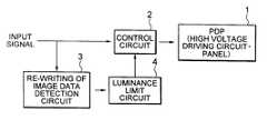
- FIG. 3is a block diagram showing a major portion of a plasma display device in accordance with a first embodiment of the present invention.
- the plasma display device in accordance with the first embodimentis provided with a control circuit 2 , which controls luminance on a plasma display panel (PDP) 1 in response to load of display (a quantity of load) read on an input signal. Also, the plasma display device is provided with a re-writing of image data detection circuit 3 , which detects whether image data in the form of an input signal into a predetermined position in the PDP 1 is re-written within a predetermined time.
- PDPplasma display panel
- the plasma display deviceis provided with a luminance limit circuit 4 , which issues a command to the control circuit 2 to shift from high luminance display (first mode), which is suitable in displaying dynamic images, to low luminance display (second mode), which is suitable in displaying fixed characters, upon judging the data has not been re-written over a certain period of time based on an output signal from the re-writing of image data detection circuit 3 .
- the PDP 1includes a high voltage driving circuit and a panel.
- the control circuit 2is provided with load-to-luminance control lookup tables used in switching the display modes of luminance based on the command from the luminance limit circuit 4 .
- FIG. 4is a graph showing a relation of load versus luminance in the plasma display device in accordance with the first embodiment of the present invention.
- an input signalis branched and sent to both the control circuit 2 and re-writing of image data detection circuit 3 .
- the re-writing of image data detection circuit 3Upon detection of a change in the input signal, the re-writing of image data detection circuit 3 outputs a signal indicating this to the luminance limit circuit 4 .
- the luminance limit circuit 4issues a command to the control circuit 2 to effect the high luminance display (first mode). Then, the control circuit 2 controls the luminance in a manner indicated by a line a in FIG. 4 with reference to the load-to-luminance control lookup table. In other words, the control circuit 2 lowers the luminance when the load of display is high, and heightens the luminance when the load of display is low.
- luminancevaries with load, and the lower the load, the higher the luminance becomes. For example, the luminance is lowered to 100 cd/m 2 at the maximum of the load (max), whereas the luminance is heightened to 300 cd/m 2 at the minimum of the load (min).
- the luminancevaries in a curve and takes a value between 100 cd/m 2 and 300 cd/m 2 when the load is somewhere between the min and max.
- the control circuit 2maintains the high luminance display (first mode) indicated by the line a. This makes it possible to achieve a display suitable in displaying dynamic images, in which the luminance at a partial highlight region is emphasized.
- the display modeis set to the high luminance display (first mode)
- the re-writing of image data detection circuit 3detects no change in the input signal over a certain period of time (for example, a few minutes)
- the re-writing of image data detection circuit 3outputs a signal indicating this to the luminance limit circuit 4 .
- the luminance limit circuit 4issues a command to the control circuit 2 to effect the low luminance display (second mode).
- the control circuit 2switches the load-to-luminance control lookup tables, and controls the luminance in a manner indicated by a line b in FIG. 4 .
- luminanceis set to a constant value in the low luminance, for example, 100 cd/m 2 , regardless of whether the load of display is high or low.
- control circuit 2controls the luminance in the manner indicated by the line a by repeating the actions discussed above.
- the plasma display devicerepeats the foregoing actions.
- the display modesare shifted between the case of displaying dynamic images, with which an input signal changes continuously, and the case of displaying a fixed pattern chiefly.
- the re-writing of image data detection circuit 3judges that the device is used chiefly to display the fixed characters, whereupon the load-to-luminance control lookup table is switched automatically and the display mode is shifted to the low luminance display (second mode, that is, fixed character display mode). Consequently, it is possible to suppress the occurrence of the image sticking by controlling the average light emission luminance and contrast while reducing influence on visibility.
- the re-writing of image data detection circuit 3judges this, and switches the display method to the one such that emphasizes the luminance and contrast partially. For this reason, not only can sharp dynamic images be displayed without impairing the display quality of the same, but also the occurrence of the image sticking can be suppressed when the fixed characters are displayed.
- the detection position in the PDP 1 where the re-writing of image data detection circuit 3 detects a change in the input signalin case that the device is chiefly used to display the fixed characters, for example, when diagrams, charts, and text information that change the screen almost entirely are displayed as the fixed characters at a conference room or the like, four corners of the display screen may be used as the detection positions, for example.
- an input signal at each detection positionis sampled, and whether there is a change in the input signal is detected, whereby the fixed character display may be distinguished from the dynamic images display.
- a predetermined portionmay be sampled.
- the samplingmay be conducted such that the display modes can be distinguished with the least number of samples on the display screen, and the samples can be of any shape including a grid, a line, a rectangle, a circle or the like.
- FIG. 5is a graph showing a relation of load versus luminance in a plasma display device in accordance with the second embodiment.
- luminance indicated by a line cwhich is lower than the line b shown in FIG. 4, is additionally provided as a level of the low luminance display, to which the display mode is shifted when no change is detected in the input signal.
- the control circuit 2switches the load-to-luminance control lookup table from the line a to the line b for the low luminance display. Further, when the re-writing of image data detection circuit 3 detects no change over a longer period of time (for example, several tens of minutes to one hour or so) from the switching, the luminance limit circuit 4 issues a command to the control circuit 2 to effect the control at the lower luminance, whereby the control circuit 2 starts to control the luminance with reference to the line c.
- a certain period of timefor example, a few minutes
- the luminance limit circuit 4issues a command to the control circuit 2 to effect the control at the lower luminance, whereby the control circuit 2 starts to control the luminance with reference to the line c.
- the second embodiment discussed aboveis suitable for use as an information board in public facilities, such as timetables at airports or train stations.
- the display patternis substantially the same, and a change occurs usually in an extremely small portion. Therefore, in order to prevent the occurrence of image sticking, the luminance has to be lowered as much as possible. Under these conditions, according to the second embodiment, the luminance can be set lower than the first embodiment, and therefore, the occurrence of the image sticking can be prevented further.
- FIG. 6is a graph showing a relation of load versus luminance in a plasma display device in accordance with the third embodiment of the present invention.
- a constant levelis set regardless of the load of display for the low luminance display, to which the display mode is shifted when no change is detected in the input signal.
- the third embodimentit is designed such that luminance varies in response to load of display also in the low luminance display, so that luminance will be heightened slightly at low load.
- the third embodiment described abovebetter visibility can be attained compared with the first embodiment while preventing the occurrence of the image sticking.
- the luminancemay drop abruptly when the control with reference to the line a shifts to the control with reference to the line b, which may result in lower visibility.
- a drop in the luminance at the low loadis smaller than that in the first embodiment, thereby improving the visibility.
- the third embodimentis suitable, for example, for use at a conference room, that is, no change is detected in the input signal over a relatively short period of time (for example, a few minutes).
Landscapes
- Engineering & Computer Science (AREA)
- Physics & Mathematics (AREA)
- Computer Hardware Design (AREA)
- General Physics & Mathematics (AREA)
- Theoretical Computer Science (AREA)
- Control Of Indicators Other Than Cathode Ray Tubes (AREA)
- Control Of Gas Discharge Display Tubes (AREA)
Abstract
Description
Claims (9)
Applications Claiming Priority (2)
| Application Number | Priority Date | Filing Date | Title |
|---|---|---|---|
| JP2000-116643 | 2000-04-18 | ||
| JP2000116643AJP4397097B2 (en) | 2000-04-18 | 2000-04-18 | Plasma display device |
Publications (2)
| Publication Number | Publication Date |
|---|---|
| US20010030513A1 US20010030513A1 (en) | 2001-10-18 |
| US6642910B2true US6642910B2 (en) | 2003-11-04 |
Family
ID=18628081
Family Applications (1)
| Application Number | Title | Priority Date | Filing Date |
|---|---|---|---|
| US09/835,572Expired - LifetimeUS6642910B2 (en) | 2000-04-18 | 2001-04-17 | Plasma display device |
Country Status (2)
| Country | Link |
|---|---|
| US (1) | US6642910B2 (en) |
| JP (1) | JP4397097B2 (en) |
Cited By (4)
| Publication number | Priority date | Publication date | Assignee | Title |
|---|---|---|---|---|
| US20070146485A1 (en)* | 2005-12-23 | 2007-06-28 | Kabushiki Kaisha Toshiba | Video display apparatus and video display method |
| US20070229400A1 (en)* | 2006-03-31 | 2007-10-04 | Fujitsu Hitachi Plasma Display Limited | Method and device for driving display device |
| US8847968B2 (en) | 2011-07-12 | 2014-09-30 | Qualcomm Incorporated | Displaying static images |
| US9218762B2 (en) | 2010-09-01 | 2015-12-22 | Qualcomm Incorporated | Dimming techniques for emissive displays |
Families Citing this family (20)
| Publication number | Priority date | Publication date | Assignee | Title |
|---|---|---|---|---|
| KR100472438B1 (en)* | 2001-11-14 | 2005-02-21 | 삼성전자주식회사 | luminance attenuator apparatus and method in the PDP |
| KR100813715B1 (en)* | 2002-01-08 | 2008-03-13 | 엘지전자 주식회사 | How to Remove Afterimages in Plasma Display Panels |
| KR100480171B1 (en)* | 2002-08-01 | 2005-04-06 | 엘지전자 주식회사 | Apparatus and method for driving plasma display panel |
| JP4079102B2 (en)* | 2003-05-22 | 2008-04-23 | ソニー株式会社 | Display device and image display method |
| JP3915738B2 (en)* | 2003-06-10 | 2007-05-16 | 株式会社日立製作所 | Display device and display method |
| JP2005189636A (en)* | 2003-12-26 | 2005-07-14 | Toshiba Matsushita Display Technology Co Ltd | Driving method and driving circuit of display device |
| KR20050025805A (en)* | 2003-09-08 | 2005-03-14 | 삼성에스디아이 주식회사 | Method for minimizing lasting image sticking in plasma display panel and plasma display panel using the same |
| KR100756584B1 (en) | 2003-11-17 | 2007-09-10 | 삼성전자주식회사 | Display device and method of removing afterimage |
| JP4788137B2 (en)* | 2004-12-09 | 2011-10-05 | 株式会社日立製作所 | Video display device |
| US7466340B1 (en)* | 2005-02-09 | 2008-12-16 | William Herz | Method and apparatus for protection against pixel burn-in |
| JP2006301556A (en)* | 2005-03-25 | 2006-11-02 | Pioneer Electronic Corp | Display apparatus |
| KR100755401B1 (en)* | 2005-06-03 | 2007-09-04 | 엘지전자 주식회사 | Plasma display panel device and driving method thereof |
| KR100761167B1 (en) | 2005-07-12 | 2007-09-21 | 엘지전자 주식회사 | Plasma display device and driving method thereof |
| JP5046355B2 (en)* | 2005-12-26 | 2012-10-10 | 東北パイオニア株式会社 | Display control apparatus and display control method for video signal |
| JP5137325B2 (en)* | 2006-04-27 | 2013-02-06 | 株式会社日立製作所 | Plasma display device and processing method thereof |
| JP2008070683A (en)* | 2006-09-15 | 2008-03-27 | Sony Corp | Image persistence suppression device, spontaneous light display device, image processing apparatus, electronic equipment, image persistence suppression method, and computer program |
| TW201928934A (en)* | 2017-12-26 | 2019-07-16 | 瑞鼎科技股份有限公司 | Display driving circuit and brightness control method applied to organic light-emitting diode panel |
| CN108550347B (en) | 2018-05-31 | 2020-11-10 | 京东方科技集团股份有限公司 | Light emission control signal generation device and display device |
| CN111261105A (en)* | 2020-03-31 | 2020-06-09 | 深圳市华星光电半导体显示技术有限公司 | Service life attenuation compensation system and compensation method of OLED device |
| US11250769B2 (en) | 2020-03-31 | 2022-02-15 | Shenzhen China Star Optoelectronics Semiconductor Display Technology Co., Ltd. | Compensation system and compensation method for life attenuation of OLED device |
Citations (7)
| Publication number | Priority date | Publication date | Assignee | Title |
|---|---|---|---|---|
| US5396443A (en)* | 1992-10-07 | 1995-03-07 | Hitachi, Ltd. | Information processing apparatus including arrangements for activation to and deactivation from a power-saving state |
| US5475847A (en)* | 1992-04-02 | 1995-12-12 | Dia Semicon Systems Incorporated | Power saving control system for computer system with feature of selective initiation of power saving control |
| US5621437A (en)* | 1994-10-07 | 1997-04-15 | Lg Electronics Inc. | Data input/output control unit for touch panel interface device |
| US5808693A (en)* | 1995-11-07 | 1998-09-15 | Sony Corporation | Video display apparatus with power saving modes |
| US6005559A (en)* | 1993-12-28 | 1999-12-21 | Canon Kabushiki Kaisha | Display apparatus with a power conserving display |
| US6144359A (en)* | 1998-03-30 | 2000-11-07 | Rockwell Science Center | Liquid crystal displays utilizing polymer dispersed liquid crystal devices for enhanced performance and reduced power |
| US6249270B1 (en)* | 1997-12-09 | 2001-06-19 | Fujitsu Limited | Liquid crystal display device, drive circuit for liquid crystal display device, and method for driving liquid crystal display device |
- 2000
- 2000-04-18JPJP2000116643Apatent/JP4397097B2/ennot_activeExpired - Fee Related
- 2001
- 2001-04-17USUS09/835,572patent/US6642910B2/ennot_activeExpired - Lifetime
Patent Citations (7)
| Publication number | Priority date | Publication date | Assignee | Title |
|---|---|---|---|---|
| US5475847A (en)* | 1992-04-02 | 1995-12-12 | Dia Semicon Systems Incorporated | Power saving control system for computer system with feature of selective initiation of power saving control |
| US5396443A (en)* | 1992-10-07 | 1995-03-07 | Hitachi, Ltd. | Information processing apparatus including arrangements for activation to and deactivation from a power-saving state |
| US6005559A (en)* | 1993-12-28 | 1999-12-21 | Canon Kabushiki Kaisha | Display apparatus with a power conserving display |
| US5621437A (en)* | 1994-10-07 | 1997-04-15 | Lg Electronics Inc. | Data input/output control unit for touch panel interface device |
| US5808693A (en)* | 1995-11-07 | 1998-09-15 | Sony Corporation | Video display apparatus with power saving modes |
| US6249270B1 (en)* | 1997-12-09 | 2001-06-19 | Fujitsu Limited | Liquid crystal display device, drive circuit for liquid crystal display device, and method for driving liquid crystal display device |
| US6144359A (en)* | 1998-03-30 | 2000-11-07 | Rockwell Science Center | Liquid crystal displays utilizing polymer dispersed liquid crystal devices for enhanced performance and reduced power |
Cited By (4)
| Publication number | Priority date | Publication date | Assignee | Title |
|---|---|---|---|---|
| US20070146485A1 (en)* | 2005-12-23 | 2007-06-28 | Kabushiki Kaisha Toshiba | Video display apparatus and video display method |
| US20070229400A1 (en)* | 2006-03-31 | 2007-10-04 | Fujitsu Hitachi Plasma Display Limited | Method and device for driving display device |
| US9218762B2 (en) | 2010-09-01 | 2015-12-22 | Qualcomm Incorporated | Dimming techniques for emissive displays |
| US8847968B2 (en) | 2011-07-12 | 2014-09-30 | Qualcomm Incorporated | Displaying static images |
Also Published As
| Publication number | Publication date |
|---|---|
| JP4397097B2 (en) | 2010-01-13 |
| JP2001306026A (en) | 2001-11-02 |
| US20010030513A1 (en) | 2001-10-18 |
Similar Documents
| Publication | Publication Date | Title |
|---|---|---|
| US6642910B2 (en) | Plasma display device | |
| JP4605630B2 (en) | Method and apparatus for compensating for burn-in on a display panel | |
| US6806852B2 (en) | Method and apparatus for driving self-emitting panel | |
| JPH1165531A (en) | Image display device and image display LSI | |
| EP1170717B1 (en) | Display device and method for driving the same | |
| JP5346426B2 (en) | Screen burn prevention method and apparatus for image display | |
| US7193598B2 (en) | Noise suppressing method for switching on/off flat panel display | |
| Kasahara et al. | 14.2: New Drive System for PDPs with Improved Image Quality: Plasma Al | |
| JPH1020838A (en) | Fluorescent screen protection circuit for image display device | |
| JP2000305514A (en) | Driving method of plasma display panel | |
| EP0945006B1 (en) | Image display device | |
| JP2003308041A (en) | Plasma display device | |
| US7952597B2 (en) | Image display device | |
| JP2001508248A (en) | Text / graphic double printing brightness control apparatus and method | |
| JP2000181429A (en) | Burning reducing device | |
| JP4797404B2 (en) | Display device | |
| EP1347434A1 (en) | Contrast and brightness control of a display | |
| US7755589B2 (en) | Noise suppressing method for flat panel display | |
| EP1414237A2 (en) | Brightness control | |
| US6686925B1 (en) | System and method for generating high-luminance windows on a computer display device | |
| KR20070066957A (en) | Increasing Color Depth, Dynamic Area, and Time Response for Electronic Displays | |
| JPH08205056A (en) | Multi-panel image display device | |
| KR100491836B1 (en) | Method AND Apparatus For controlling Average Picture Level in Plasma Display Panel | |
| US7327332B2 (en) | Plasma display panel video processing circuit and method and video display device and method using plasma display panel | |
| KR20030060279A (en) | Method for minimizing image sticking effect of a plasma display panel |
Legal Events
| Date | Code | Title | Description |
|---|---|---|---|
| AS | Assignment | Owner name:NEC CORPORATION, JAPAN Free format text:ASSIGNMENT OF ASSIGNORS INTEREST;ASSIGNORS:TAKADA, HIDEKAZU;UEOKA, MITSUO;REEL/FRAME:011715/0945 Effective date:20010411 | |
| STCF | Information on status: patent grant | Free format text:PATENTED CASE | |
| FEPP | Fee payment procedure | Free format text:PAYOR NUMBER ASSIGNED (ORIGINAL EVENT CODE: ASPN); ENTITY STATUS OF PATENT OWNER: LARGE ENTITY | |
| AS | Assignment | Owner name:NEC PLASMA DISPLAY CORPORATION, JAPAN Free format text:ASSIGNMENT OF ASSIGNORS INTEREST;ASSIGNOR:NEC CORPORATION;REEL/FRAME:015931/0301 Effective date:20040930 | |
| AS | Assignment | Owner name:PIONEER PLASMA DISPLAY CORPORATION, JAPAN Free format text:ASSIGNMENT OF ASSIGNORS INTEREST;ASSIGNOR:NEC PLASMA DISPLAY CORPORATION;REEL/FRAME:016038/0801 Effective date:20040930 | |
| AS | Assignment | Owner name:PIONEER CORPORATION,JAPAN Free format text:ASSIGNMENT OF ASSIGNORS INTEREST;ASSIGNOR:PIONEER PLASMA DISPLAY CORPORATION;REEL/FRAME:016334/0922 Effective date:20050531 Owner name:PIONEER CORPORATION, JAPAN Free format text:ASSIGNMENT OF ASSIGNORS INTEREST;ASSIGNOR:PIONEER PLASMA DISPLAY CORPORATION;REEL/FRAME:016334/0922 Effective date:20050531 | |
| FPAY | Fee payment | Year of fee payment:4 | |
| AS | Assignment | Owner name:PANASONIC CORPORATION, JAPAN Free format text:ASSIGNMENT OF ASSIGNORS INTEREST;ASSIGNOR:PIONEER CORPORATION (FORMERLY CALLED PIONEER ELECTRONIC CORPORATION);REEL/FRAME:023234/0173 Effective date:20090907 | |
| FPAY | Fee payment | Year of fee payment:8 | |
| FEPP | Fee payment procedure | Free format text:PAYER NUMBER DE-ASSIGNED (ORIGINAL EVENT CODE: RMPN); ENTITY STATUS OF PATENT OWNER: LARGE ENTITY | |
| FPAY | Fee payment | Year of fee payment:12 |