US6642102B2 - Barrier material encapsulation of programmable material - Google Patents
Barrier material encapsulation of programmable materialDownload PDFInfo
- Publication number
- US6642102B2 US6642102B2US09/896,530US89653001AUS6642102B2US 6642102 B2US6642102 B2US 6642102B2US 89653001 AUS89653001 AUS 89653001AUS 6642102 B2US6642102 B2US 6642102B2
- Authority
- US
- United States
- Prior art keywords
- dielectric material
- forming
- programmable
- opening
- signal line
- Prior art date
- Legal status (The legal status is an assumption and is not a legal conclusion. Google has not performed a legal analysis and makes no representation as to the accuracy of the status listed.)
- Expired - Lifetime
Links
- 239000000463materialSubstances0.000titleclaimsabstractdescription90
- 230000004888barrier functionEffects0.000titledescription7
- 238000005538encapsulationMethods0.000title1
- 239000003989dielectric materialSubstances0.000claimsabstractdescription88
- 239000000758substrateSubstances0.000claimsabstractdescription22
- 238000000034methodMethods0.000claimsabstractdescription21
- 238000005530etchingMethods0.000claimsabstractdescription12
- 238000002161passivationMethods0.000claimsdescription11
- 150000004770chalcogenidesChemical class0.000claimsdescription8
- 239000012782phase change materialSubstances0.000claimsdescription7
- 229910052782aluminiumInorganic materials0.000claimsdescription2
- XAGFODPZIPBFFR-UHFFFAOYSA-NaluminiumChemical compound[Al]XAGFODPZIPBFFR-UHFFFAOYSA-N0.000claimsdescription2
- AZDRQVAHHNSJOQ-UHFFFAOYSA-NalumaneChemical group[AlH3]AZDRQVAHHNSJOQ-UHFFFAOYSA-N0.000claims1
- VYPSYNLAJGMNEJ-UHFFFAOYSA-NSilicium dioxideChemical compoundO=[Si]=OVYPSYNLAJGMNEJ-UHFFFAOYSA-N0.000description20
- 239000004020conductorSubstances0.000description18
- 238000002955isolationMethods0.000description16
- 239000000377silicon dioxideSubstances0.000description10
- 229910052581Si3N4Inorganic materials0.000description8
- XUIMIQQOPSSXEZ-UHFFFAOYSA-NSiliconChemical compound[Si]XUIMIQQOPSSXEZ-UHFFFAOYSA-N0.000description8
- 239000003638chemical reducing agentSubstances0.000description8
- 229910052710siliconInorganic materials0.000description8
- 239000010703siliconSubstances0.000description8
- HQVNEWCFYHHQES-UHFFFAOYSA-Nsilicon nitrideChemical compoundN12[Si]34N5[Si]62N3[Si]51N64HQVNEWCFYHHQES-UHFFFAOYSA-N0.000description8
- 239000002019doping agentSubstances0.000description7
- 230000008859changeEffects0.000description6
- 235000012239silicon dioxideNutrition0.000description6
- 239000010936titaniumSubstances0.000description4
- 230000015572biosynthetic processEffects0.000description3
- 230000005669field effectEffects0.000description3
- -1i.e.Substances0.000description3
- 239000004065semiconductorSubstances0.000description3
- RTAQQCXQSZGOHL-UHFFFAOYSA-NTitaniumChemical compound[Ti]RTAQQCXQSZGOHL-UHFFFAOYSA-N0.000description2
- NRTOMJZYCJJWKI-UHFFFAOYSA-NTitanium nitrideChemical compound[Ti]#NNRTOMJZYCJJWKI-UHFFFAOYSA-N0.000description2
- 238000005229chemical vapour depositionMethods0.000description2
- 229910017052cobaltInorganic materials0.000description2
- 239000010941cobaltSubstances0.000description2
- GUTLYIVDDKVIGB-UHFFFAOYSA-Ncobalt atomChemical compound[Co]GUTLYIVDDKVIGB-UHFFFAOYSA-N0.000description2
- 238000010586diagramMethods0.000description2
- 239000007772electrode materialSubstances0.000description2
- 238000004519manufacturing processMethods0.000description2
- 239000003870refractory metalSubstances0.000description2
- 229910021332silicideInorganic materials0.000description2
- FVBUAEGBCNSCDD-UHFFFAOYSA-Nsilicide(4-)Chemical compound[Si-4]FVBUAEGBCNSCDD-UHFFFAOYSA-N0.000description2
- 229910052719titaniumInorganic materials0.000description2
- 229910000838Al alloyInorganic materials0.000description1
- OKTJSMMVPCPJKN-UHFFFAOYSA-NCarbonChemical compound[C]OKTJSMMVPCPJKN-UHFFFAOYSA-N0.000description1
- UQZIWOQVLUASCR-UHFFFAOYSA-Nalumane;titaniumChemical compound[AlH3].[Ti]UQZIWOQVLUASCR-UHFFFAOYSA-N0.000description1
- 229910052787antimonyInorganic materials0.000description1
- 229910052785arsenicInorganic materials0.000description1
- RQNWIZPPADIBDY-UHFFFAOYSA-Narsenic atomChemical compound[As]RQNWIZPPADIBDY-UHFFFAOYSA-N0.000description1
- 229910052799carbonInorganic materials0.000description1
- 229910010293ceramic materialInorganic materials0.000description1
- 238000006243chemical reactionMethods0.000description1
- 239000003795chemical substances by applicationSubstances0.000description1
- 238000005516engineering processMethods0.000description1
- 230000008020evaporationEffects0.000description1
- 238000001704evaporationMethods0.000description1
- 239000011521glassSubstances0.000description1
- BHEPBYXIRTUNPN-UHFFFAOYSA-Nhydridophosphorus(.) (triplet)Chemical compound[PH]BHEPBYXIRTUNPN-UHFFFAOYSA-N0.000description1
- 230000006872improvementEffects0.000description1
- 230000002452interceptive effectEffects0.000description1
- 229910052751metalInorganic materials0.000description1
- 239000002184metalSubstances0.000description1
- 238000004377microelectronicMethods0.000description1
- 239000000203mixtureSubstances0.000description1
- 238000012986modificationMethods0.000description1
- 230000004048modificationEffects0.000description1
- 239000011368organic materialSubstances0.000description1
- 238000000059patterningMethods0.000description1
- 230000002093peripheral effectEffects0.000description1
- 229910021420polycrystalline siliconInorganic materials0.000description1
- 230000008569processEffects0.000description1
- 230000000717retained effectEffects0.000description1
- 239000007787solidSubstances0.000description1
- 238000001228spectrumMethods0.000description1
- 230000003068static effectEffects0.000description1
- 239000010409thin filmSubstances0.000description1
- MAKDTFFYCIMFQP-UHFFFAOYSA-Ntitanium tungstenChemical compound[Ti].[W]MAKDTFFYCIMFQP-UHFFFAOYSA-N0.000description1
- 229910052723transition metalInorganic materials0.000description1
- 150000003624transition metalsChemical class0.000description1
- WFKWXMTUELFFGS-UHFFFAOYSA-NtungstenChemical compound[W]WFKWXMTUELFFGS-UHFFFAOYSA-N0.000description1
- 229910052721tungstenInorganic materials0.000description1
- 239000010937tungstenSubstances0.000description1
Images


Classifications
- H—ELECTRICITY
- H01—ELECTRIC ELEMENTS
- H01L—SEMICONDUCTOR DEVICES NOT COVERED BY CLASS H10
- H01L21/00—Processes or apparatus adapted for the manufacture or treatment of semiconductor or solid state devices or of parts thereof
- H01L21/70—Manufacture or treatment of devices consisting of a plurality of solid state components formed in or on a common substrate or of parts thereof; Manufacture of integrated circuit devices or of parts thereof
- H01L21/71—Manufacture of specific parts of devices defined in group H01L21/70
- H01L21/768—Applying interconnections to be used for carrying current between separate components within a device comprising conductors and dielectrics
- H01L21/76897—Formation of self-aligned vias or contact plugs, i.e. involving a lithographically uncritical step
- H—ELECTRICITY
- H10—SEMICONDUCTOR DEVICES; ELECTRIC SOLID-STATE DEVICES NOT OTHERWISE PROVIDED FOR
- H10B—ELECTRONIC MEMORY DEVICES
- H10B63/00—Resistance change memory devices, e.g. resistive RAM [ReRAM] devices
- H10B63/20—Resistance change memory devices, e.g. resistive RAM [ReRAM] devices comprising selection components having two electrodes, e.g. diodes
- H—ELECTRICITY
- H10—SEMICONDUCTOR DEVICES; ELECTRIC SOLID-STATE DEVICES NOT OTHERWISE PROVIDED FOR
- H10N—ELECTRIC SOLID-STATE DEVICES NOT OTHERWISE PROVIDED FOR
- H10N70/00—Solid-state devices having no potential barriers, and specially adapted for rectifying, amplifying, oscillating or switching
- H10N70/011—Manufacture or treatment of multistable switching devices
- H10N70/061—Shaping switching materials
- H10N70/063—Shaping switching materials by etching of pre-deposited switching material layers, e.g. lithography
- H—ELECTRICITY
- H10—SEMICONDUCTOR DEVICES; ELECTRIC SOLID-STATE DEVICES NOT OTHERWISE PROVIDED FOR
- H10N—ELECTRIC SOLID-STATE DEVICES NOT OTHERWISE PROVIDED FOR
- H10N70/00—Solid-state devices having no potential barriers, and specially adapted for rectifying, amplifying, oscillating or switching
- H10N70/20—Multistable switching devices, e.g. memristors
- H10N70/231—Multistable switching devices, e.g. memristors based on solid-state phase change, e.g. between amorphous and crystalline phases, Ovshinsky effect
- H—ELECTRICITY
- H10—SEMICONDUCTOR DEVICES; ELECTRIC SOLID-STATE DEVICES NOT OTHERWISE PROVIDED FOR
- H10N—ELECTRIC SOLID-STATE DEVICES NOT OTHERWISE PROVIDED FOR
- H10N70/00—Solid-state devices having no potential barriers, and specially adapted for rectifying, amplifying, oscillating or switching
- H10N70/801—Constructional details of multistable switching devices
- H10N70/821—Device geometry
- H10N70/826—Device geometry adapted for essentially vertical current flow, e.g. sandwich or pillar type devices
- H—ELECTRICITY
- H10—SEMICONDUCTOR DEVICES; ELECTRIC SOLID-STATE DEVICES NOT OTHERWISE PROVIDED FOR
- H10N—ELECTRIC SOLID-STATE DEVICES NOT OTHERWISE PROVIDED FOR
- H10N70/00—Solid-state devices having no potential barriers, and specially adapted for rectifying, amplifying, oscillating or switching
- H10N70/801—Constructional details of multistable switching devices
- H10N70/841—Electrodes
- H—ELECTRICITY
- H10—SEMICONDUCTOR DEVICES; ELECTRIC SOLID-STATE DEVICES NOT OTHERWISE PROVIDED FOR
- H10N—ELECTRIC SOLID-STATE DEVICES NOT OTHERWISE PROVIDED FOR
- H10N70/00—Solid-state devices having no potential barriers, and specially adapted for rectifying, amplifying, oscillating or switching
- H10N70/801—Constructional details of multistable switching devices
- H10N70/881—Switching materials
- H10N70/882—Compounds of sulfur, selenium or tellurium, e.g. chalcogenides
- H10N70/8828—Tellurides, e.g. GeSbTe
- H—ELECTRICITY
- H01—ELECTRIC ELEMENTS
- H01L—SEMICONDUCTOR DEVICES NOT COVERED BY CLASS H10
- H01L23/00—Details of semiconductor or other solid state devices
- H01L23/52—Arrangements for conducting electric current within the device in operation from one component to another, i.e. interconnections, e.g. wires, lead frames
- H01L23/522—Arrangements for conducting electric current within the device in operation from one component to another, i.e. interconnections, e.g. wires, lead frames including external interconnections consisting of a multilayer structure of conductive and insulating layers inseparably formed on the semiconductor body
- H01L23/525—Arrangements for conducting electric current within the device in operation from one component to another, i.e. interconnections, e.g. wires, lead frames including external interconnections consisting of a multilayer structure of conductive and insulating layers inseparably formed on the semiconductor body with adaptable interconnections
- H—ELECTRICITY
- H01—ELECTRIC ELEMENTS
- H01L—SEMICONDUCTOR DEVICES NOT COVERED BY CLASS H10
- H01L2924/00—Indexing scheme for arrangements or methods for connecting or disconnecting semiconductor or solid-state bodies as covered by H01L24/00
- H01L2924/0001—Technical content checked by a classifier
- H01L2924/0002—Not covered by any one of groups H01L24/00, H01L24/00 and H01L2224/00
- Y—GENERAL TAGGING OF NEW TECHNOLOGICAL DEVELOPMENTS; GENERAL TAGGING OF CROSS-SECTIONAL TECHNOLOGIES SPANNING OVER SEVERAL SECTIONS OF THE IPC; TECHNICAL SUBJECTS COVERED BY FORMER USPC CROSS-REFERENCE ART COLLECTIONS [XRACs] AND DIGESTS
- Y10—TECHNICAL SUBJECTS COVERED BY FORMER USPC
- Y10S—TECHNICAL SUBJECTS COVERED BY FORMER USPC CROSS-REFERENCE ART COLLECTIONS [XRACs] AND DIGESTS
- Y10S438/00—Semiconductor device manufacturing: process
- Y10S438/90—Bulk effect device making
Definitions
- the inventionrelates generally to programmable devices.
- Typical memory applicationsinclude dynamic random access memory (DRAM), static random access memory (SRAM), erasable programmable read only memory (EPROM), and electrically erasable programmable read only memory (EEPROM).
- DRAMdynamic random access memory
- SRAMstatic random access memory
- EPROMerasable programmable read only memory
- EEPROMelectrically erasable programmable read only memory
- Solid state memory devicestypically employ micro-electronic circuit elements for each memory bit (e.g., one to four transistors per bit) in memory applications. Since one or more electronic circuit elements are required for each memory bit, these devices may consume considerable chip “real estate” to store a bit of information, which limits the density of a memory chip.
- the primary “non-volatile” memory element of these devicessuch as an EEPROM, typically employ a floating gate field effect transistor device that has limited re-programmability and which holds a charge on the gate of field effect transistor to store each memory bit. These classes of memory devices are also relatively slow to program.
- Phase change memory devicesuse phase change materials, i.e., materials that can be electrically switched between a generally amorphous and a generally crystalline state, for electronic memory application.
- phase change materialsi.e., materials that can be electrically switched between a generally amorphous and a generally crystalline state
- One type of memory element originally developed by Energy Conversion Devices, Inc. of Troy, Mich.utilizes a phase change material that can be, in one application, electrically switched between a structural state of generally amorphous and generally crystalline local order or between different detectable states of local order across the entire spectrum between completely amorphous and completely crystalline states.
- Typical materials suitable for such applicationinclude those utilizing various chalcogenide elements.
- These electrical memory devicestypically do not use field effect transistor devices, but comprise, in the electrical context, a monolithic body of thin film chalcogenide material.
- phase change memory materialsrepresent a significant improvement in non-volatile memory.
- phase change programmable devicessuch as phase change memory devices
- signal linese.g., row and column lines
- an electrodee.g., an electrode
- an isolation devicebetween a signal line and the programmable material.
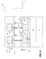
- FIG. 1is a schematic diagram of an array of programmable elements.
- FIG. 2shows a cross-sectional view of a portion of a semiconductor structure having programmable device cells formed therein, each cell including at this point, an isolation device and an electrode coupled to a signal line.
- FIG. 3shows a cross-sectional view of the structure of FIG. 2 further including a programmable material and a second signal line.
- FIG. 4shows the structure of FIG. 3 following the introduction of a first dielectric layer and a second dielectric layer over the superior surface of the structure.
- FIG. 5shows the structure of FIGS. 4 following the forming of a contact to a signal line.
- the methodincludes forming, as stacked materials on a substrate, a volume of programmable material and a signal line.
- the methodalso includes conformably forming a first dielectric material on the stacked materials and form a second dielectric material on the first material.
- An openingis etched in the second dielectric material with an etchant that, between the first dielectric material and the second dielectric material, favors removal of the second dielectric material. Following the etching of an opening, a contact is formed to the stacked materials.
- an apparatusin another embodiment, includes a contact point formed on a substrate and a volume of programmable material formed on the contact point.
- a signal lineis formed on the volume of programmable material and a first and second dielectric material overlie the signal line with a contact formed through the first and second dielectric materials to the signal line.
- the embodimentdescribes a programmable material including a phase change material wherein the phase of the material determines the state of the memory element (e.g., 0 or 1).
- FIG. 1shows a schematic diagram of an embodiment of a memory array comprised of a plurality of memory elements.
- the circuit of memory array 5includes an xz grid with a plurality of memory elements 30 electrically interconnected in series with a plurality of isolation devices 25 on a portion of a chip.
- Address lines 10e.g., columns
- 20e.g., rows
- One purpose of the xz grid array of memory elements in combination with isolation devicesis to enable each discrete memory element to be read and written without interfering with the information stored in adjacent or remote memory elements of the array.
- a memory array such as memory array 5may be formed in a portion, including the entire portion, of a substrate.
- a typical substrateincludes a semiconductor substrate such as a silicon substrate.
- Other substratesincluding, but not limited to, substrates that contain ceramic material, organic material, or glass material as part of the infrastructure are also suitable.
- memory array 5may be fabricated over an area of the substrate at the wafer level and then the wafer reduced through singulation into discrete die or chips, some or all of the die or chips having a memory array formed thereon. Additional addressing circuitry (e.g., decoders, etc.) may be formed in a similar fashion.
- FIGS. 2-5illustrate the fabrication of representative memory element 15 of FIG. 1 .
- FIG. 2shows substrate 110 of structure 100 representatively doped such that substrate 110 includes P ++ portion (e.g., P-type dopant on the order of 5 ⁇ 10 19 to 1 ⁇ 10 20 atoms per cubic centimeters (atoms/cm 3 ).
- P ++ portione.g., P-type dopant on the order of 5 ⁇ 10 19 to 1 ⁇ 10 20 atoms per cubic centimeters (atoms/cm 3 ).
- portion 120 of P-type epitaxial silicone.g., dopant concentration on the order of 10 16 to 10 17 atoms/cm 3 ).
- First conductor or signal line material 140is N-type doped silicon formed by the introduction of, for example, phosphorous or arsenic to a concentration on the order of about 10 18 to 10 19 atoms/cm 3 (e.g., N + silicon).
- first conductor or signal line material 140serves as an address line, a row line (e.g., row line 20 of FIG. 1 ).
- Device cells 200 A and 200 Boverlie first conductor or signal line material 140 .
- device cell 200 Arepresents memory element 15 of FIG. 1 .
- first conductor or signal line material 140 in each of device cell 200 A and device cell 200 Bis an isolation device (e.g., isolation device 25 of FIG. 1 in device cell 200 A).
- the isolation deviceis a PN diode formed of N-type silicon portion 150 (dopant concentration on the order of about 10 17 to 10 18 atoms/cm 3 ) and P-type silicon portion 160 (dopant concentration on the order of about 10 19 to 10 20 atom cm 3 ).
- a z-direction dimension (not shown) of device cell 200 A and device 200 Bmay be established prior to the formation of first conductor or signal line 140 and isolation device 25 .
- the z-direction dimensionmay be formed by shallow trench isolation (STI) structures.
- the x-direction dimension of device cells 200 A and 200 Bmay be formed, again by STI techniques.
- FIG. 2shows trenches formed adjacent device cells 200 A and 200 B. Following trench formation, N-type dopant may be introduced between device cells (e.g., between device cells 200 A and 200 B) to form pockets 195 having a dopant concentration on the order of about 10 18 to 10 20 atoms/cm 3 (e.g., N + region).
- FIG. 2shows dielectric material 205 of, for example, silicon dioxide (SiO 2 ) as STI structures between device cells 200 A and 200 B.
- reducer material 170of, in this example, a refractory metal silicide such as cobalt silicide (CoSi 2 ).
- Reducer material 170serves as a low resistance material in the fabrication of peripheral circuitry (e.g., addressing circuitry) of the circuit structure on the chip in this instance.
- peripheral circuitrye.g., addressing circuitry
- reducer material 170is not required in terms of forming a memory element as described. Nevertheless, because of its generally low resistance property, its inclusion is part of the programmable cell structure between isolation device 25 and a memory element is utilized in this embodiment.
- Reducer material 170may be formed by introducing a refractory metal (e.g., cobalt) into a portion of P-type silicon portion 160 .
- dielectric material 180overlies reducer material 170 and serves, in one embodiment, as an etch stop for a subsequent opening to reducer material 170 .
- Dielectric material 180is, for example, silicon nitride (Si 3 N 4 ).
- dielectric material 210is silicon dioxide (SiO 2 ).
- Electrode 270is formed through dielectric material 210 to reducer material 170 . Electrode 270 is formed, for example, by forming an opening through dielectric material 210 to reducer material 170 and lining the opening with electrode material. Dielectric material removed in forming the opening may then be replaced adjacent the electrode along the sidewall of the opening.
- a suitable material for electrode 270includes polycrystalline silicon.
- Other suitable materialsinclude carbon and semi-metals such as transition metals including, but not limited to, titanium (Ti), titanium-tungsten (TiW), titanium nitride (TiN) and titanium aluminum nitride (TiAlN). Dopants or other agents may be added to electrode 270 , for example, at its superior tip (as viewed) to modify the resistance of the electrode material.
- the superior surface of the structurein this example, may be planarized, if necessary, such as by chemical-mechanical polish. Following planarization, superior end 275 of electrode 270 is exposed.
- FIG. 3shows the structure of FIG. 2 following the introduction of programmable material 290 in device cells 200 A and 200 B.
- programmable material 290is a phase change material.
- programmable material 290includes a chalcogenide element (s).
- phase change programmable material 290include, but are not limited to, compositions of the class of tellerium-germanium-antimony (Te x Ge y Sb z ) material.
- Programmable material 290in one example according to current technology, is introduced to a thickness on the order of about 600 ⁇ .
- barrier materials 300 and 310of, for example, titanium (Ti) and titanium nitride (TiN), respectively.
- second conductor or signal line material 315Overlying barrier materials 300 and 310 is second conductor or signal line material 315 .
- second conductor or signal line material 315serves as an address line, a column line.
- Second conductor or signal line material 315is, for example, an aluminum material, such as an aluminum alloy.
- second conductor or signal line material 315is patterned to be, in one embodiment, generally orthogonal to first conductor or signal line material 140 .
- FIG. 4shows the structure of FIG. 3 following the introduction of first dielectric material 325 .
- first dielectric material 325is conformably introduced over the superior surface (as viewed) of structure 100 .
- First dielectric materialis, for example, silicon nitride introduced by chemical vapor deposition (CVD).
- First dielectric material 325is introduced to a representative thickness sufficient to encapsulate programmable material 290 between dielectric material 210 , first dielectric material 325 , and second conductor or signal line material 315 (and barrier materials 300 and 310 ).
- First dielectric material 325may be selected such that it protects programmable material 290 during thermal processing.
- chalcogenide materialstend to evaporate at thermal processing temperatures greater than 450° C.
- First dielectric material 325 of, for example, silicon nitrideencapsulates the chalcogenide material (programmable material 290 ) and inhibits evaporation during subsequent thermal processing of structure 100 .
- Second dielectric materialis introduced, in one embodiment, to a sufficient thickness to allow for planarization.
- Second dielectric material 330is selected such that, between first dielectric material 325 and second dielectric material 330 , second dielectric material 330 may be selectively or favorably removed.
- the material properties for first dielectric material 325 and second dielectric material 330are such that an etchant may be selected that favors removal of second dielectric material 330 over first dielectric material 325 .
- first dielectric material 325is silicon nitride (Si 3 N 4 )
- second dielectric material 330is for example, silicon dioxide (SiO 2 ).
- FIG. 5shows the structure of FIG. 4 following the forming of a contact to second conductor or signal line material 315 .
- Forming a contact to second conductor or signal line material 315may be desired where, in the example of a memory array, it is desired to couple the signal line (column line) to addressing circuitry.
- FIG. 5shows opening 340 formed in second dielectric material 330 .
- Opening 340proceeds to second conductor or signal line material 315 and therefore an opening is also made in first dielectric material 325 .
- Contact plug 350 of, for example, tungstenis formed in opening 340 .
- opening 340may be formed through etch patterning whereby a pattern mask (not shown) defines an opening area for opening 340 and an etchant selectively removes within the opening area.
- the etchantis selected such that it favors the etching of second dielectric material 330 over first dielectric material 325 . In such manner, when the etchant encounters first dielectric material 325 , etching stops or is significantly slowed.
- a suitable etchant where first dielectric material 325 is silicon nitride and second dielectric material 330 is silicon dioxideis, for example, CF 4 /H 2 .
- FIG. 5shows opening 340 misaligned over second conductor or signal line material 315 .
- first dielectric material 325may act as a barrier layer.
- the barrier layerinhibits the etching or removal of dielectric material to programmable material 290 .
- first dielectric material 325acts as a barrier layer to address this concern.
- FIG. 1the representative array of FIG. 1 and the representative programmable device structure(s) of FIGS. 2-5 is one example of an apparatus wherein the programmable material may be encapsulated in passivation layers. It is appreciated, that the passivation technique may be used in other areas where, for example, alignment issues or thermal protection is desired.
- the specification and drawingsare, accordingly, to be regarded in an illustrated rather than a restrictive sense.
Landscapes
- Engineering & Computer Science (AREA)
- Manufacturing & Machinery (AREA)
- Physics & Mathematics (AREA)
- Condensed Matter Physics & Semiconductors (AREA)
- General Physics & Mathematics (AREA)
- Computer Hardware Design (AREA)
- Microelectronics & Electronic Packaging (AREA)
- Power Engineering (AREA)
- Semiconductor Memories (AREA)
Abstract
Description
Claims (13)
Priority Applications (2)
| Application Number | Priority Date | Filing Date | Title |
|---|---|---|---|
| US09/896,530US6642102B2 (en) | 2001-06-30 | 2001-06-30 | Barrier material encapsulation of programmable material |
| US10/418,548US7064344B2 (en) | 2001-06-30 | 2003-04-17 | Barrier material encapsulation of programmable material |
Applications Claiming Priority (1)
| Application Number | Priority Date | Filing Date | Title |
|---|---|---|---|
| US09/896,530US6642102B2 (en) | 2001-06-30 | 2001-06-30 | Barrier material encapsulation of programmable material |
Related Child Applications (1)
| Application Number | Title | Priority Date | Filing Date |
|---|---|---|---|
| US10/418,548DivisionUS7064344B2 (en) | 2001-06-30 | 2003-04-17 | Barrier material encapsulation of programmable material |
Publications (2)
| Publication Number | Publication Date |
|---|---|
| US20030003709A1 US20030003709A1 (en) | 2003-01-02 |
| US6642102B2true US6642102B2 (en) | 2003-11-04 |
Family
ID=25406369
Family Applications (2)
| Application Number | Title | Priority Date | Filing Date |
|---|---|---|---|
| US09/896,530Expired - LifetimeUS6642102B2 (en) | 2001-06-30 | 2001-06-30 | Barrier material encapsulation of programmable material |
| US10/418,548Expired - Fee RelatedUS7064344B2 (en) | 2001-06-30 | 2003-04-17 | Barrier material encapsulation of programmable material |
Family Applications After (1)
| Application Number | Title | Priority Date | Filing Date |
|---|---|---|---|
| US10/418,548Expired - Fee RelatedUS7064344B2 (en) | 2001-06-30 | 2003-04-17 | Barrier material encapsulation of programmable material |
Country Status (1)
| Country | Link |
|---|---|
| US (2) | US6642102B2 (en) |
Cited By (80)
| Publication number | Priority date | Publication date | Assignee | Title |
|---|---|---|---|---|
| US6791885B2 (en) | 2002-02-19 | 2004-09-14 | Micron Technology, Inc. | Programmable conductor random access memory and method for sensing same |
| US6809362B2 (en) | 2002-02-20 | 2004-10-26 | Micron Technology, Inc. | Multiple data state memory cell |
| US20040211957A1 (en)* | 2002-08-29 | 2004-10-28 | Moore John T. | Method and apparatus for controlling metal doping of a chalcogenide memory element |
| US6813178B2 (en) | 2003-03-12 | 2004-11-02 | Micron Technology, Inc. | Chalcogenide glass constant current device, and its method of fabrication and operation |
| US6812087B2 (en) | 2002-01-31 | 2004-11-02 | Micron Technology, Inc. | Methods of forming non-volatile resistance variable devices and methods of forming silver selenide comprising structures |
| US6815818B2 (en)* | 2001-11-19 | 2004-11-09 | Micron Technology, Inc. | Electrode structure for use in an integrated circuit |
| US6833559B2 (en) | 2001-02-08 | 2004-12-21 | Micron Technology, Inc. | Non-volatile resistance variable device |
| US6849868B2 (en) | 2002-03-14 | 2005-02-01 | Micron Technology, Inc. | Methods and apparatus for resistance variable material cells |
| US6855975B2 (en) | 2002-04-10 | 2005-02-15 | Micron Technology, Inc. | Thin film diode integrated with chalcogenide memory cell |
| US6856002B2 (en) | 2002-08-29 | 2005-02-15 | Micron Technology, Inc. | Graded GexSe100-x concentration in PCRAM |
| US6858482B2 (en) | 2002-04-10 | 2005-02-22 | Micron Technology, Inc. | Method of manufacture of programmable switching circuits and memory cells employing a glass layer |
| US6858465B2 (en) | 2002-06-06 | 2005-02-22 | Micron Technology, Inc. | Elimination of dendrite formation during metal/chalcogenide glass deposition |
| US6864521B2 (en) | 2002-08-29 | 2005-03-08 | Micron Technology, Inc. | Method to control silver concentration in a resistance variable memory element |
| US6864500B2 (en) | 2002-04-10 | 2005-03-08 | Micron Technology, Inc. | Programmable conductor memory cell structure |
| US6867996B2 (en) | 2002-08-29 | 2005-03-15 | Micron Technology, Inc. | Single-polarity programmable resistance-variable memory element |
| US6867064B2 (en) | 2002-02-15 | 2005-03-15 | Micron Technology, Inc. | Method to alter chalcogenide glass for improved switching characteristics |
| US6867114B2 (en) | 2002-08-29 | 2005-03-15 | Micron Technology Inc. | Methods to form a memory cell with metal-rich metal chalcogenide |
| US6873538B2 (en) | 2001-12-20 | 2005-03-29 | Micron Technology, Inc. | Programmable conductor random access memory and a method for writing thereto |
| US6878569B2 (en) | 2001-03-15 | 2005-04-12 | Micron Technology, Inc. | Agglomeration elimination for metal sputter deposition of chalcogenides |
| US6882578B2 (en) | 2002-01-04 | 2005-04-19 | Micron Technology, Inc. | PCRAM rewrite prevention |
| US6888155B2 (en) | 2001-08-30 | 2005-05-03 | Micron Technology, Inc. | Stoichiometry for chalcogenide glasses useful for memory devices and method of formation |
| US6890790B2 (en) | 2002-06-06 | 2005-05-10 | Micron Technology, Inc. | Co-sputter deposition of metal-doped chalcogenides |
| US6891749B2 (en) | 2002-02-20 | 2005-05-10 | Micron Technology, Inc. | Resistance variable ‘on ’ memory |
| US6894304B2 (en) | 2001-08-27 | 2005-05-17 | Micron Technology, Inc. | Apparatus and method for dual cell common electrode PCRAM memory device |
| US6903361B2 (en) | 2003-09-17 | 2005-06-07 | Micron Technology, Inc. | Non-volatile memory structure |
| US6930909B2 (en) | 2003-06-25 | 2005-08-16 | Micron Technology, Inc. | Memory device and methods of controlling resistance variation and resistance profile drift |
| US6937528B2 (en) | 2002-03-05 | 2005-08-30 | Micron Technology, Inc. | Variable resistance memory and method for sensing same |
| US6949402B2 (en) | 2001-03-01 | 2005-09-27 | Micron Technology, Inc. | Method of forming a non-volatile resistance variable device |
| US6951805B2 (en) | 2001-08-01 | 2005-10-04 | Micron Technology, Inc. | Method of forming integrated circuitry, method of forming memory circuitry, and method of forming random access memory circuitry |
| US6955940B2 (en) | 2001-08-29 | 2005-10-18 | Micron Technology, Inc. | Method of forming chalcogenide comprising devices |
| US6961277B2 (en) | 2003-07-08 | 2005-11-01 | Micron Technology, Inc. | Method of refreshing a PCRAM memory device |
| US20050263823A1 (en)* | 2004-05-27 | 2005-12-01 | Young-Nam Hwang | Phase-change memory device having a barrier layer and manufacturing method |
| US20050263801A1 (en)* | 2004-05-27 | 2005-12-01 | Jae-Hyun Park | Phase-change memory device having a barrier layer and manufacturing method |
| US20050263829A1 (en)* | 2004-05-27 | 2005-12-01 | Yoon-Jong Song | Semiconductor devices having phase change memory cells, electronic systems employing the same and methods of fabricating the same |
| US6998697B2 (en) | 2001-08-29 | 2006-02-14 | Micron Technology, Inc. | Non-volatile resistance variable devices |
| US7002833B2 (en) | 2001-11-20 | 2006-02-21 | Micron Technology, Inc. | Complementary bit resistance memory sensor and method of operation |
| US7010644B2 (en) | 2002-08-29 | 2006-03-07 | Micron Technology, Inc. | Software refreshed memory device and method |
| US7015494B2 (en) | 2002-07-10 | 2006-03-21 | Micron Technology, Inc. | Assemblies displaying differential negative resistance |
| US7018863B2 (en) | 2002-08-22 | 2006-03-28 | Micron Technology, Inc. | Method of manufacture of a resistance variable memory cell |
| US7022579B2 (en) | 2003-03-14 | 2006-04-04 | Micron Technology, Inc. | Method for filling via with metal |
| US7049009B2 (en) | 2002-08-29 | 2006-05-23 | Micron Technology, Inc. | Silver selenide film stoichiometry and morphology control in sputter deposition |
| US7050327B2 (en) | 2003-04-10 | 2006-05-23 | Micron Technology, Inc. | Differential negative resistance memory |
| US7061004B2 (en) | 2003-07-21 | 2006-06-13 | Micron Technology, Inc. | Resistance variable memory elements and methods of formation |
| US7071021B2 (en) | 2001-05-11 | 2006-07-04 | Micron Technology, Inc. | PCRAM memory cell and method of making same |
| US7087919B2 (en) | 2002-02-20 | 2006-08-08 | Micron Technology, Inc. | Layered resistance variable memory device and method of fabrication |
| US7094700B2 (en) | 2002-08-29 | 2006-08-22 | Micron Technology, Inc. | Plasma etching methods and methods of forming memory devices comprising a chalcogenide comprising layer received operably proximate conductive electrodes |
| US7098068B2 (en) | 2004-03-10 | 2006-08-29 | Micron Technology, Inc. | Method of forming a chalcogenide material containing device |
| US7105864B2 (en) | 2004-01-29 | 2006-09-12 | Micron Technology, Inc. | Non-volatile zero field splitting resonance memory |
| US20060239058A1 (en)* | 2005-04-22 | 2006-10-26 | Micron Technology, Inc. | Method and apparatus for accessing a memory array |
| US7151688B2 (en) | 2004-09-01 | 2006-12-19 | Micron Technology, Inc. | Sensing of resistance variable memory devices |
| US7153721B2 (en) | 2004-01-28 | 2006-12-26 | Micron Technology, Inc. | Resistance variable memory elements based on polarized silver-selenide network growth |
| US7190048B2 (en) | 2004-07-19 | 2007-03-13 | Micron Technology, Inc. | Resistance variable memory device and method of fabrication |
| US7209378B2 (en) | 2002-08-08 | 2007-04-24 | Micron Technology, Inc. | Columnar 1T-N memory cell structure |
| US7233520B2 (en) | 2005-07-08 | 2007-06-19 | Micron Technology, Inc. | Process for erasing chalcogenide variable resistance memory bits |
| US7251154B2 (en) | 2005-08-15 | 2007-07-31 | Micron Technology, Inc. | Method and apparatus providing a cross-point memory array using a variable resistance memory cell and capacitance |
| US7269079B2 (en) | 2005-05-16 | 2007-09-11 | Micron Technology, Inc. | Power circuits for reducing a number of power supply voltage taps required for sensing a resistive memory |
| US7274034B2 (en) | 2005-08-01 | 2007-09-25 | Micron Technology, Inc. | Resistance variable memory device with sputtered metal-chalcogenide region and method of fabrication |
| US7277313B2 (en) | 2005-08-31 | 2007-10-02 | Micron Technology, Inc. | Resistance variable memory element with threshold device and method of forming the same |
| US7294527B2 (en) | 2002-08-29 | 2007-11-13 | Micron Technology Inc. | Method of forming a memory cell |
| US7304368B2 (en) | 2005-08-11 | 2007-12-04 | Micron Technology, Inc. | Chalcogenide-based electrokinetic memory element and method of forming the same |
| US20070290185A1 (en)* | 2006-06-15 | 2007-12-20 | Industrial Technology Research Institute | Phase change memory cells and methods for fabricating the same |
| US7317200B2 (en) | 2005-02-23 | 2008-01-08 | Micron Technology, Inc. | SnSe-based limited reprogrammable cell |
| US7317567B2 (en) | 2005-08-02 | 2008-01-08 | Micron Technology, Inc. | Method and apparatus for providing color changing thin film material |
| US7326950B2 (en) | 2004-07-19 | 2008-02-05 | Micron Technology, Inc. | Memory device with switching glass layer |
| US7332735B2 (en) | 2005-08-02 | 2008-02-19 | Micron Technology, Inc. | Phase change memory cell and method of formation |
| US7354793B2 (en) | 2004-08-12 | 2008-04-08 | Micron Technology, Inc. | Method of forming a PCRAM device incorporating a resistance-variable chalocogenide element |
| US7365411B2 (en) | 2004-08-12 | 2008-04-29 | Micron Technology, Inc. | Resistance variable memory with temperature tolerant materials |
| US7374174B2 (en) | 2004-12-22 | 2008-05-20 | Micron Technology, Inc. | Small electrode for resistance variable devices |
| US7396699B2 (en) | 2001-08-29 | 2008-07-08 | Micron Technology, Inc. | Method of forming non-volatile resistance variable devices and method of forming a programmable memory cell of memory circuitry |
| US7427770B2 (en) | 2005-04-22 | 2008-09-23 | Micron Technology, Inc. | Memory array for increased bit density |
| US7579615B2 (en) | 2005-08-09 | 2009-08-25 | Micron Technology, Inc. | Access transistor for memory device |
| US7583551B2 (en) | 2004-03-10 | 2009-09-01 | Micron Technology, Inc. | Power management control and controlling memory refresh operations |
| US7663133B2 (en) | 2005-04-22 | 2010-02-16 | Micron Technology, Inc. | Memory elements having patterned electrodes and method of forming the same |
| US7723713B2 (en) | 2002-02-20 | 2010-05-25 | Micron Technology, Inc. | Layered resistance variable memory device and method of fabrication |
| US7791058B2 (en) | 2006-08-29 | 2010-09-07 | Micron Technology, Inc. | Enhanced memory density resistance variable memory cells, arrays, devices and systems including the same, and methods of fabrication |
| US7863173B2 (en)* | 2007-06-20 | 2011-01-04 | Samsung Electronics Co., Ltd. | Variable resistance non-volatile memory cells and methods of fabricating same |
| US20120228577A1 (en)* | 2011-03-11 | 2012-09-13 | Park Kyusul | Phase change memory device and method of manufacturing the same |
| US8467236B2 (en) | 2008-08-01 | 2013-06-18 | Boise State University | Continuously variable resistor |
| US9406881B1 (en) | 2015-04-24 | 2016-08-02 | Micron Technology, Inc. | Memory cells having a heater electrode formed between a first storage material and a second storage material and methods of forming the same |
| US9691912B1 (en)* | 2012-09-20 | 2017-06-27 | University Of South Florida | Devices having nanoscale structures and methods for making same |
Families Citing this family (6)
| Publication number | Priority date | Publication date | Assignee | Title |
|---|---|---|---|---|
| TWI284899B (en)* | 2005-12-29 | 2007-08-01 | Ind Tech Res Inst | Semiconductor memory device, phase change memory device and method of manufacturing the same |
| US8030128B1 (en)* | 2007-04-23 | 2011-10-04 | Marvell International Ltd. | Method to form high density phase change memory (PCM) top contact every two bits |
| KR101161178B1 (en)* | 2007-09-07 | 2012-07-02 | 타이완 세미콘덕터 매뉴팩쳐링 컴퍼니 리미티드 | An electronic component, and a method of manufacturing an electronic component |
| TWI426604B (en)* | 2008-06-03 | 2014-02-11 | Higgs Opl Capital Llc | Phase-change memory devices and methods for fabricating the same |
| FR3112018A1 (en)* | 2020-06-30 | 2021-12-31 | Stmicroelectronics (Rousset) Sas | Phase change memory cell isolation |
| CN116093067B (en)* | 2021-11-03 | 2025-09-05 | 长鑫存储技术有限公司 | Fuse structure, forming method and programmable memory |
Citations (15)
| Publication number | Priority date | Publication date | Assignee | Title |
|---|---|---|---|---|
| US4597162A (en)* | 1983-01-18 | 1986-07-01 | Energy Conversion Devices, Inc. | Method for making, parallel preprogramming or field programming of electronic matrix arrays |
| US5296716A (en) | 1991-01-18 | 1994-03-22 | Energy Conversion Devices, Inc. | Electrically erasable, directly overwritable, multibit single cell memory elements and arrays fabricated therefrom |
| US5335219A (en)* | 1991-01-18 | 1994-08-02 | Ovshinsky Stanford R | Homogeneous composition of microcrystalline semiconductor material, semiconductor devices and directly overwritable memory elements fabricated therefrom, and arrays fabricated from the memory elements |
| US5596522A (en)* | 1991-01-18 | 1997-01-21 | Energy Conversion Devices, Inc. | Homogeneous compositions of microcrystalline semiconductor material, semiconductor devices and directly overwritable memory elements fabricated therefrom, and arrays fabricated from the memory elements |
| US5751012A (en)* | 1995-06-07 | 1998-05-12 | Micron Technology, Inc. | Polysilicon pillar diode for use in a non-volatile memory cell |
| US5789758A (en) | 1995-06-07 | 1998-08-04 | Micron Technology, Inc. | Chalcogenide memory cell with a plurality of chalcogenide electrodes |
| US5879955A (en) | 1995-06-07 | 1999-03-09 | Micron Technology, Inc. | Method for fabricating an array of ultra-small pores for chalcogenide memory cells |
| US5933365A (en)* | 1997-06-19 | 1999-08-03 | Energy Conversion Devices, Inc. | Memory element with energy control mechanism |
| US5970336A (en) | 1996-08-22 | 1999-10-19 | Micron Technology, Inc. | Method of making memory cell incorporating a chalcogenide element |
| US6031287A (en) | 1997-06-18 | 2000-02-29 | Micron Technology, Inc. | Contact structure and memory element incorporating the same |
| US6087674A (en) | 1996-10-28 | 2000-07-11 | Energy Conversion Devices, Inc. | Memory element with memory material comprising phase-change material and dielectric material |
| US6114713A (en)* | 1997-01-28 | 2000-09-05 | Zahorik; Russell C. | Integrated circuit memory cell having a small active area and method of forming same |
| US6229157B1 (en)* | 1996-06-18 | 2001-05-08 | Micron Technology, Inc. | Method of forming a polysilicon diode and devices incorporating such diode |
| US6337266B1 (en)* | 1996-07-22 | 2002-01-08 | Micron Technology, Inc. | Small electrode for chalcogenide memories |
| US6429449B1 (en)* | 1995-06-07 | 2002-08-06 | Micron Technology, Inc. | Three-dimensional container diode for use with multi-state material in a non-volatile memory cell |
Family Cites Families (8)
| Publication number | Priority date | Publication date | Assignee | Title |
|---|---|---|---|---|
| US4115872A (en)* | 1977-05-31 | 1978-09-19 | Burroughs Corporation | Amorphous semiconductor memory device for employment in an electrically alterable read-only memory |
| US4203123A (en)* | 1977-12-12 | 1980-05-13 | Burroughs Corporation | Thin film memory device employing amorphous semiconductor materials |
| JPH03173126A (en)* | 1989-11-30 | 1991-07-26 | Mitsubishi Electric Corp | Semiconductor device of multilayer film structure and its manufacture |
| US5166758A (en)* | 1991-01-18 | 1992-11-24 | Energy Conversion Devices, Inc. | Electrically erasable phase change memory |
| US5536947A (en)* | 1991-01-18 | 1996-07-16 | Energy Conversion Devices, Inc. | Electrically erasable, directly overwritable, multibit single cell memory element and arrays fabricated therefrom |
| US5682058A (en)* | 1994-03-31 | 1997-10-28 | Crosspoint Solutions, Inc. | Multilayer antifuse with low leakage and method of manufacture therefor |
| US6653733B1 (en)* | 1996-02-23 | 2003-11-25 | Micron Technology, Inc. | Conductors in semiconductor devices |
| US6649928B2 (en)* | 2000-12-13 | 2003-11-18 | Intel Corporation | Method to selectively remove one side of a conductive bottom electrode of a phase-change memory cell and structure obtained thereby |
- 2001
- 2001-06-30USUS09/896,530patent/US6642102B2/ennot_activeExpired - Lifetime
- 2003
- 2003-04-17USUS10/418,548patent/US7064344B2/ennot_activeExpired - Fee Related
Patent Citations (20)
| Publication number | Priority date | Publication date | Assignee | Title |
|---|---|---|---|---|
| US4597162A (en)* | 1983-01-18 | 1986-07-01 | Energy Conversion Devices, Inc. | Method for making, parallel preprogramming or field programming of electronic matrix arrays |
| US5296716A (en) | 1991-01-18 | 1994-03-22 | Energy Conversion Devices, Inc. | Electrically erasable, directly overwritable, multibit single cell memory elements and arrays fabricated therefrom |
| US5335219A (en)* | 1991-01-18 | 1994-08-02 | Ovshinsky Stanford R | Homogeneous composition of microcrystalline semiconductor material, semiconductor devices and directly overwritable memory elements fabricated therefrom, and arrays fabricated from the memory elements |
| US5596522A (en)* | 1991-01-18 | 1997-01-21 | Energy Conversion Devices, Inc. | Homogeneous compositions of microcrystalline semiconductor material, semiconductor devices and directly overwritable memory elements fabricated therefrom, and arrays fabricated from the memory elements |
| US5751012A (en)* | 1995-06-07 | 1998-05-12 | Micron Technology, Inc. | Polysilicon pillar diode for use in a non-volatile memory cell |
| US5789758A (en) | 1995-06-07 | 1998-08-04 | Micron Technology, Inc. | Chalcogenide memory cell with a plurality of chalcogenide electrodes |
| US5879955A (en) | 1995-06-07 | 1999-03-09 | Micron Technology, Inc. | Method for fabricating an array of ultra-small pores for chalcogenide memory cells |
| US5920788A (en) | 1995-06-07 | 1999-07-06 | Micron Technology, Inc. | Chalcogenide memory cell with a plurality of chalcogenide electrodes |
| US6429449B1 (en)* | 1995-06-07 | 2002-08-06 | Micron Technology, Inc. | Three-dimensional container diode for use with multi-state material in a non-volatile memory cell |
| US6002140A (en) | 1995-06-07 | 1999-12-14 | Micron Technology, Inc. | Method for fabricating an array of ultra-small pores for chalcogenide memory cells |
| US6229157B1 (en)* | 1996-06-18 | 2001-05-08 | Micron Technology, Inc. | Method of forming a polysilicon diode and devices incorporating such diode |
| US6337266B1 (en)* | 1996-07-22 | 2002-01-08 | Micron Technology, Inc. | Small electrode for chalcogenide memories |
| US5998244A (en) | 1996-08-22 | 1999-12-07 | Micron Technology, Inc. | Memory cell incorporating a chalcogenide element and method of making same |
| US6153890A (en) | 1996-08-22 | 2000-11-28 | Micron Technology, Inc. | Memory cell incorporating a chalcogenide element |
| US5970336A (en) | 1996-08-22 | 1999-10-19 | Micron Technology, Inc. | Method of making memory cell incorporating a chalcogenide element |
| US6087674A (en) | 1996-10-28 | 2000-07-11 | Energy Conversion Devices, Inc. | Memory element with memory material comprising phase-change material and dielectric material |
| US6114713A (en)* | 1997-01-28 | 2000-09-05 | Zahorik; Russell C. | Integrated circuit memory cell having a small active area and method of forming same |
| US6287919B1 (en)* | 1997-01-28 | 2001-09-11 | Micron Technology, Inc. | Integrated circuit memory cell having a small active area and method of forming same |
| US6031287A (en) | 1997-06-18 | 2000-02-29 | Micron Technology, Inc. | Contact structure and memory element incorporating the same |
| US5933365A (en)* | 1997-06-19 | 1999-08-03 | Energy Conversion Devices, Inc. | Memory element with energy control mechanism |
Cited By (175)
| Publication number | Priority date | Publication date | Assignee | Title |
|---|---|---|---|---|
| US6833559B2 (en) | 2001-02-08 | 2004-12-21 | Micron Technology, Inc. | Non-volatile resistance variable device |
| US7030410B2 (en) | 2001-02-08 | 2006-04-18 | Micron Technology, Inc. | Resistance variable device |
| US6949402B2 (en) | 2001-03-01 | 2005-09-27 | Micron Technology, Inc. | Method of forming a non-volatile resistance variable device |
| US7199444B2 (en) | 2001-03-01 | 2007-04-03 | Micron Technology, Inc. | Memory device, programmable resistance memory cell and memory array |
| US7022555B2 (en) | 2001-03-01 | 2006-04-04 | Micron Technology, Inc. | Methods of forming a semiconductor memory device |
| US6974965B2 (en) | 2001-03-15 | 2005-12-13 | Micron Technology, Inc. | Agglomeration elimination for metal sputter deposition of chalcogenides |
| US7528401B2 (en) | 2001-03-15 | 2009-05-05 | Micron Technology, Inc. | Agglomeration elimination for metal sputter deposition of chalcogenides |
| US6949453B2 (en) | 2001-03-15 | 2005-09-27 | Micron Technology, Inc. | Agglomeration elimination for metal sputter deposition of chalcogenides |
| US6878569B2 (en) | 2001-03-15 | 2005-04-12 | Micron Technology, Inc. | Agglomeration elimination for metal sputter deposition of chalcogenides |
| US7235419B2 (en) | 2001-05-11 | 2007-06-26 | Micron Technology, Inc. | Method of making a memory cell |
| US7071021B2 (en) | 2001-05-11 | 2006-07-04 | Micron Technology, Inc. | PCRAM memory cell and method of making same |
| US7687793B2 (en) | 2001-05-11 | 2010-03-30 | Micron Technology, Inc. | Resistance variable memory cells |
| US6951805B2 (en) | 2001-08-01 | 2005-10-04 | Micron Technology, Inc. | Method of forming integrated circuitry, method of forming memory circuitry, and method of forming random access memory circuitry |
| US6894304B2 (en) | 2001-08-27 | 2005-05-17 | Micron Technology, Inc. | Apparatus and method for dual cell common electrode PCRAM memory device |
| US7396699B2 (en) | 2001-08-29 | 2008-07-08 | Micron Technology, Inc. | Method of forming non-volatile resistance variable devices and method of forming a programmable memory cell of memory circuitry |
| US6955940B2 (en) | 2001-08-29 | 2005-10-18 | Micron Technology, Inc. | Method of forming chalcogenide comprising devices |
| US7348205B2 (en) | 2001-08-29 | 2008-03-25 | Micron Technology, Inc. | Method of forming resistance variable devices |
| US7863597B2 (en) | 2001-08-29 | 2011-01-04 | Micron Technology, Inc. | Resistance variable memory devices with passivating material |
| US6998697B2 (en) | 2001-08-29 | 2006-02-14 | Micron Technology, Inc. | Non-volatile resistance variable devices |
| US6888155B2 (en) | 2001-08-30 | 2005-05-03 | Micron Technology, Inc. | Stoichiometry for chalcogenide glasses useful for memory devices and method of formation |
| US6815818B2 (en)* | 2001-11-19 | 2004-11-09 | Micron Technology, Inc. | Electrode structure for use in an integrated circuit |
| US7115992B2 (en) | 2001-11-19 | 2006-10-03 | Micron Technology, Inc. | Electrode structure for use in an integrated circuit |
| US7115504B2 (en) | 2001-11-19 | 2006-10-03 | Micron Technology, Inc. | Method of forming electrode structure for use in an integrated circuit |
| US7332401B2 (en) | 2001-11-19 | 2008-02-19 | Micron Technology, Ing. | Method of fabricating an electrode structure for use in an integrated circuit |
| US7869249B2 (en) | 2001-11-20 | 2011-01-11 | Micron Technology, Inc. | Complementary bit PCRAM sense amplifier and method of operation |
| US7002833B2 (en) | 2001-11-20 | 2006-02-21 | Micron Technology, Inc. | Complementary bit resistance memory sensor and method of operation |
| US7242603B2 (en) | 2001-11-20 | 2007-07-10 | Micron Technology, Inc. | Method of operating a complementary bit resistance memory sensor |
| US7366003B2 (en) | 2001-11-20 | 2008-04-29 | Micron Technology, Inc. | Method of operating a complementary bit resistance memory sensor and method of operation |
| US6873538B2 (en) | 2001-12-20 | 2005-03-29 | Micron Technology, Inc. | Programmable conductor random access memory and a method for writing thereto |
| US6909656B2 (en) | 2002-01-04 | 2005-06-21 | Micron Technology, Inc. | PCRAM rewrite prevention |
| US6882578B2 (en) | 2002-01-04 | 2005-04-19 | Micron Technology, Inc. | PCRAM rewrite prevention |
| US7224632B2 (en) | 2002-01-04 | 2007-05-29 | Micron Technology, Inc. | Rewrite prevention in a variable resistance memory |
| US6812087B2 (en) | 2002-01-31 | 2004-11-02 | Micron Technology, Inc. | Methods of forming non-volatile resistance variable devices and methods of forming silver selenide comprising structures |
| US6867064B2 (en) | 2002-02-15 | 2005-03-15 | Micron Technology, Inc. | Method to alter chalcogenide glass for improved switching characteristics |
| US6791885B2 (en) | 2002-02-19 | 2004-09-14 | Micron Technology, Inc. | Programmable conductor random access memory and method for sensing same |
| US6954385B2 (en) | 2002-02-19 | 2005-10-11 | Micron Technology, Inc. | Method and apparatus for sensing resistive memory state |
| US7723713B2 (en) | 2002-02-20 | 2010-05-25 | Micron Technology, Inc. | Layered resistance variable memory device and method of fabrication |
| US7087919B2 (en) | 2002-02-20 | 2006-08-08 | Micron Technology, Inc. | Layered resistance variable memory device and method of fabrication |
| US8263958B2 (en) | 2002-02-20 | 2012-09-11 | Micron Technology, Inc. | Layered resistance variable memory device and method of fabrication |
| US7202520B2 (en) | 2002-02-20 | 2007-04-10 | Micron Technology, Inc. | Multiple data state memory cell |
| US6891749B2 (en) | 2002-02-20 | 2005-05-10 | Micron Technology, Inc. | Resistance variable ‘on ’ memory |
| US7498231B2 (en) | 2002-02-20 | 2009-03-03 | Micron Technology, Inc. | Multiple data state memory cell |
| US6809362B2 (en) | 2002-02-20 | 2004-10-26 | Micron Technology, Inc. | Multiple data state memory cell |
| US6908808B2 (en) | 2002-02-20 | 2005-06-21 | Micron Technology, Inc. | Method of forming and storing data in a multiple state memory cell |
| US6937528B2 (en) | 2002-03-05 | 2005-08-30 | Micron Technology, Inc. | Variable resistance memory and method for sensing same |
| US6849868B2 (en) | 2002-03-14 | 2005-02-01 | Micron Technology, Inc. | Methods and apparatus for resistance variable material cells |
| US6855975B2 (en) | 2002-04-10 | 2005-02-15 | Micron Technology, Inc. | Thin film diode integrated with chalcogenide memory cell |
| US6858482B2 (en) | 2002-04-10 | 2005-02-22 | Micron Technology, Inc. | Method of manufacture of programmable switching circuits and memory cells employing a glass layer |
| US7479650B2 (en) | 2002-04-10 | 2009-01-20 | Micron Technology, Inc. | Method of manufacture of programmable conductor memory |
| US6864500B2 (en) | 2002-04-10 | 2005-03-08 | Micron Technology, Inc. | Programmable conductor memory cell structure |
| US7112484B2 (en) | 2002-04-10 | 2006-09-26 | Micron Technology, Inc. | Thin film diode integrated with chalcogenide memory cell |
| US7547905B2 (en) | 2002-04-10 | 2009-06-16 | Micron Technology, Inc. | Programmable conductor memory cell structure and method therefor |
| US7202104B2 (en) | 2002-06-06 | 2007-04-10 | Micron Technology, Inc. | Co-sputter deposition of metal-doped chalcogenides |
| US6858465B2 (en) | 2002-06-06 | 2005-02-22 | Micron Technology, Inc. | Elimination of dendrite formation during metal/chalcogenide glass deposition |
| US7446393B2 (en) | 2002-06-06 | 2008-11-04 | Micron Technology, Inc. | Co-sputter deposition of metal-doped chalcogenides |
| US6890790B2 (en) | 2002-06-06 | 2005-05-10 | Micron Technology, Inc. | Co-sputter deposition of metal-doped chalcogenides |
| US7964436B2 (en) | 2002-06-06 | 2011-06-21 | Round Rock Research, Llc | Co-sputter deposition of metal-doped chalcogenides |
| US7015494B2 (en) | 2002-07-10 | 2006-03-21 | Micron Technology, Inc. | Assemblies displaying differential negative resistance |
| US7879646B2 (en) | 2002-07-10 | 2011-02-01 | Micron Technology, Inc. | Assemblies displaying differential negative resistance, semiconductor constructions, and methods of forming assemblies displaying differential negative resistance |
| US7209378B2 (en) | 2002-08-08 | 2007-04-24 | Micron Technology, Inc. | Columnar 1T-N memory cell structure |
| US7459764B2 (en) | 2002-08-22 | 2008-12-02 | Micron Technology, Inc. | Method of manufacture of a PCRAM memory cell |
| US7550818B2 (en) | 2002-08-22 | 2009-06-23 | Micron Technology, Inc. | Method of manufacture of a PCRAM memory cell |
| US7018863B2 (en) | 2002-08-22 | 2006-03-28 | Micron Technology, Inc. | Method of manufacture of a resistance variable memory cell |
| US7223627B2 (en) | 2002-08-29 | 2007-05-29 | Micron Technology, Inc. | Memory element and its method of formation |
| US9552986B2 (en) | 2002-08-29 | 2017-01-24 | Micron Technology, Inc. | Forming a memory device using sputtering to deposit silver-selenide film |
| US7010644B2 (en) | 2002-08-29 | 2006-03-07 | Micron Technology, Inc. | Software refreshed memory device and method |
| US7163837B2 (en) | 2002-08-29 | 2007-01-16 | Micron Technology, Inc. | Method of forming a resistance variable memory element |
| US20040211957A1 (en)* | 2002-08-29 | 2004-10-28 | Moore John T. | Method and apparatus for controlling metal doping of a chalcogenide memory element |
| US7564731B2 (en) | 2002-08-29 | 2009-07-21 | Micron Technology, Inc. | Software refreshed memory device and method |
| US7944768B2 (en) | 2002-08-29 | 2011-05-17 | Micron Technology, Inc. | Software refreshed memory device and method |
| US7364644B2 (en) | 2002-08-29 | 2008-04-29 | Micron Technology, Inc. | Silver selenide film stoichiometry and morphology control in sputter deposition |
| US6953720B2 (en) | 2002-08-29 | 2005-10-11 | Micron Technology, Inc. | Methods for forming chalcogenide glass-based memory elements |
| US7049009B2 (en) | 2002-08-29 | 2006-05-23 | Micron Technology, Inc. | Silver selenide film stoichiometry and morphology control in sputter deposition |
| US6856002B2 (en) | 2002-08-29 | 2005-02-15 | Micron Technology, Inc. | Graded GexSe100-x concentration in PCRAM |
| US7307908B2 (en) | 2002-08-29 | 2007-12-11 | Micron Technology, Inc. | Software refreshed memory device and method |
| US7056762B2 (en) | 2002-08-29 | 2006-06-06 | Micron Technology, Inc. | Methods to form a memory cell with metal-rich metal chalcogenide |
| US20050148150A1 (en)* | 2002-08-29 | 2005-07-07 | Moore John T. | Memory element and its method of formation |
| US7768861B2 (en) | 2002-08-29 | 2010-08-03 | Micron Technology, Inc. | Software refreshed memory device and method |
| US7692177B2 (en) | 2002-08-29 | 2010-04-06 | Micron Technology, Inc. | Resistance variable memory element and its method of formation |
| US7094700B2 (en) | 2002-08-29 | 2006-08-22 | Micron Technology, Inc. | Plasma etching methods and methods of forming memory devices comprising a chalcogenide comprising layer received operably proximate conductive electrodes |
| US6867114B2 (en) | 2002-08-29 | 2005-03-15 | Micron Technology Inc. | Methods to form a memory cell with metal-rich metal chalcogenide |
| US7518212B2 (en) | 2002-08-29 | 2009-04-14 | Micron Technology, Inc. | Graded GexSe100-x concentration in PCRAM |
| US6867996B2 (en) | 2002-08-29 | 2005-03-15 | Micron Technology, Inc. | Single-polarity programmable resistance-variable memory element |
| US6864521B2 (en) | 2002-08-29 | 2005-03-08 | Micron Technology, Inc. | Method to control silver concentration in a resistance variable memory element |
| US7087454B2 (en) | 2002-08-29 | 2006-08-08 | Micron Technology, Inc. | Fabrication of single polarity programmable resistance structure |
| US7294527B2 (en) | 2002-08-29 | 2007-11-13 | Micron Technology Inc. | Method of forming a memory cell |
| US6813178B2 (en) | 2003-03-12 | 2004-11-02 | Micron Technology, Inc. | Chalcogenide glass constant current device, and its method of fabrication and operation |
| US7022579B2 (en) | 2003-03-14 | 2006-04-04 | Micron Technology, Inc. | Method for filling via with metal |
| US7050327B2 (en) | 2003-04-10 | 2006-05-23 | Micron Technology, Inc. | Differential negative resistance memory |
| US7745808B2 (en) | 2003-04-10 | 2010-06-29 | Micron Technology, Inc. | Differential negative resistance memory |
| US7329558B2 (en) | 2003-04-10 | 2008-02-12 | Micron Technology, Inc. | Differential negative resistance memory |
| US6930909B2 (en) | 2003-06-25 | 2005-08-16 | Micron Technology, Inc. | Memory device and methods of controlling resistance variation and resistance profile drift |
| US7385868B2 (en) | 2003-07-08 | 2008-06-10 | Micron Technology, Inc. | Method of refreshing a PCRAM memory device |
| US6961277B2 (en) | 2003-07-08 | 2005-11-01 | Micron Technology, Inc. | Method of refreshing a PCRAM memory device |
| US7061004B2 (en) | 2003-07-21 | 2006-06-13 | Micron Technology, Inc. | Resistance variable memory elements and methods of formation |
| US7491963B2 (en) | 2003-09-17 | 2009-02-17 | Micron Technology, Inc. | Non-volatile memory structure |
| US7276722B2 (en) | 2003-09-17 | 2007-10-02 | Micron Technology, Inc. | Non-volatile memory structure |
| US6903361B2 (en) | 2003-09-17 | 2005-06-07 | Micron Technology, Inc. | Non-volatile memory structure |
| US6946347B2 (en) | 2003-09-17 | 2005-09-20 | Micron Technology, Inc. | Non-volatile memory structure |
| US7153721B2 (en) | 2004-01-28 | 2006-12-26 | Micron Technology, Inc. | Resistance variable memory elements based on polarized silver-selenide network growth |
| US7105864B2 (en) | 2004-01-29 | 2006-09-12 | Micron Technology, Inc. | Non-volatile zero field splitting resonance memory |
| US7459336B2 (en) | 2004-03-10 | 2008-12-02 | Micron Technology, Inc. | Method of forming a chalcogenide material containing device |
| US8619485B2 (en) | 2004-03-10 | 2013-12-31 | Round Rock Research, Llc | Power management control and controlling memory refresh operations |
| US7098068B2 (en) | 2004-03-10 | 2006-08-29 | Micron Technology, Inc. | Method of forming a chalcogenide material containing device |
| US7583551B2 (en) | 2004-03-10 | 2009-09-01 | Micron Technology, Inc. | Power management control and controlling memory refresh operations |
| US9142263B2 (en) | 2004-03-10 | 2015-09-22 | Round Rock Research, Llc | Power management control and controlling memory refresh operations |
| US7482616B2 (en)* | 2004-05-27 | 2009-01-27 | Samsung Electronics Co., Ltd. | Semiconductor devices having phase change memory cells, electronic systems employing the same and methods of fabricating the same |
| US7411208B2 (en) | 2004-05-27 | 2008-08-12 | Samsung Electronics Co., Ltd. | Phase-change memory device having a barrier layer and manufacturing method |
| US20050263801A1 (en)* | 2004-05-27 | 2005-12-01 | Jae-Hyun Park | Phase-change memory device having a barrier layer and manufacturing method |
| US20050263823A1 (en)* | 2004-05-27 | 2005-12-01 | Young-Nam Hwang | Phase-change memory device having a barrier layer and manufacturing method |
| US20050263829A1 (en)* | 2004-05-27 | 2005-12-01 | Yoon-Jong Song | Semiconductor devices having phase change memory cells, electronic systems employing the same and methods of fabricating the same |
| US8026543B2 (en) | 2004-05-27 | 2011-09-27 | Samsung Electronics Co., Ltd. | Semiconductor devices having phase change memory cells, electronic systems employing the same and methods of fabricating the same |
| US20090101881A1 (en)* | 2004-05-27 | 2009-04-23 | Samsung Electronics Co., Ltd. | Semiconductor devices having phase change memory cells, electronic systems employing the same and methods of fabricating the same |
| US7348209B2 (en) | 2004-07-19 | 2008-03-25 | Micron Technology, Inc. | Resistance variable memory device and method of fabrication |
| US7190048B2 (en) | 2004-07-19 | 2007-03-13 | Micron Technology, Inc. | Resistance variable memory device and method of fabrication |
| US7282783B2 (en) | 2004-07-19 | 2007-10-16 | Micron Technology, Inc. | Resistance variable memory device and method of fabrication |
| US7326950B2 (en) | 2004-07-19 | 2008-02-05 | Micron Technology, Inc. | Memory device with switching glass layer |
| US7749853B2 (en) | 2004-07-19 | 2010-07-06 | Microntechnology, Inc. | Method of forming a variable resistance memory device comprising tin selenide |
| US7759665B2 (en) | 2004-07-19 | 2010-07-20 | Micron Technology, Inc. | PCRAM device with switching glass layer |
| US8895401B2 (en) | 2004-08-12 | 2014-11-25 | Micron Technology, Inc. | Method of forming a memory device incorporating a resistance variable chalcogenide element |
| US7682992B2 (en) | 2004-08-12 | 2010-03-23 | Micron Technology, Inc. | Resistance variable memory with temperature tolerant materials |
| US7924603B2 (en) | 2004-08-12 | 2011-04-12 | Micron Technology, Inc. | Resistance variable memory with temperature tolerant materials |
| US7354793B2 (en) | 2004-08-12 | 2008-04-08 | Micron Technology, Inc. | Method of forming a PCRAM device incorporating a resistance-variable chalocogenide element |
| US8334186B2 (en) | 2004-08-12 | 2012-12-18 | Micron Technology, Inc. | Method of forming a memory device incorporating a resistance variable chalcogenide element |
| US7365411B2 (en) | 2004-08-12 | 2008-04-29 | Micron Technology, Inc. | Resistance variable memory with temperature tolerant materials |
| US7785976B2 (en) | 2004-08-12 | 2010-08-31 | Micron Technology, Inc. | Method of forming a memory device incorporating a resistance-variable chalcogenide element |
| US7586777B2 (en) | 2004-08-12 | 2009-09-08 | Micron Technology, Inc. | Resistance variable memory with temperature tolerant materials |
| US8487288B2 (en) | 2004-08-12 | 2013-07-16 | Micron Technology, Inc. | Memory device incorporating a resistance variable chalcogenide element |
| US7393798B2 (en) | 2004-08-12 | 2008-07-01 | Micron Technology, Inc. | Resistance variable memory with temperature tolerant materials |
| US7994491B2 (en) | 2004-08-12 | 2011-08-09 | Micron Technology, Inc. | PCRAM device with switching glass layer |
| US7190608B2 (en) | 2004-09-01 | 2007-03-13 | Micron Technology, Inc. | Sensing of resistance variable memory devices |
| US7151688B2 (en) | 2004-09-01 | 2006-12-19 | Micron Technology, Inc. | Sensing of resistance variable memory devices |
| US7910397B2 (en) | 2004-12-22 | 2011-03-22 | Micron Technology, Inc. | Small electrode for resistance variable devices |
| US7374174B2 (en) | 2004-12-22 | 2008-05-20 | Micron Technology, Inc. | Small electrode for resistance variable devices |
| US7317200B2 (en) | 2005-02-23 | 2008-01-08 | Micron Technology, Inc. | SnSe-based limited reprogrammable cell |
| US8101936B2 (en) | 2005-02-23 | 2012-01-24 | Micron Technology, Inc. | SnSe-based limited reprogrammable cell |
| US7968927B2 (en) | 2005-04-22 | 2011-06-28 | Micron Technology, Inc. | Memory array for increased bit density and method of forming the same |
| US7700422B2 (en) | 2005-04-22 | 2010-04-20 | Micron Technology, Inc. | Methods of forming memory arrays for increased bit density |
| US7663133B2 (en) | 2005-04-22 | 2010-02-16 | Micron Technology, Inc. | Memory elements having patterned electrodes and method of forming the same |
| US7709289B2 (en) | 2005-04-22 | 2010-05-04 | Micron Technology, Inc. | Memory elements having patterned electrodes and method of forming the same |
| US20060239058A1 (en)* | 2005-04-22 | 2006-10-26 | Micron Technology, Inc. | Method and apparatus for accessing a memory array |
| US7427770B2 (en) | 2005-04-22 | 2008-09-23 | Micron Technology, Inc. | Memory array for increased bit density |
| US7269044B2 (en) | 2005-04-22 | 2007-09-11 | Micron Technology, Inc. | Method and apparatus for accessing a memory array |
| US7366045B2 (en) | 2005-05-16 | 2008-04-29 | Micron Technology, Inc. | Power circuits for reducing a number of power supply voltage taps required for sensing a resistive memory |
| US7269079B2 (en) | 2005-05-16 | 2007-09-11 | Micron Technology, Inc. | Power circuits for reducing a number of power supply voltage taps required for sensing a resistive memory |
| US7551509B2 (en) | 2005-05-16 | 2009-06-23 | Micron Technology, Inc. | Power circuits for reducing a number of power supply voltage taps required for sensing a resistive memory |
| US7643333B2 (en) | 2005-07-08 | 2010-01-05 | Micron Technology, Inc. | Process for erasing chalcogenide variable resistance memory bits |
| US7233520B2 (en) | 2005-07-08 | 2007-06-19 | Micron Technology, Inc. | Process for erasing chalcogenide variable resistance memory bits |
| US7274034B2 (en) | 2005-08-01 | 2007-09-25 | Micron Technology, Inc. | Resistance variable memory device with sputtered metal-chalcogenide region and method of fabrication |
| US7940556B2 (en) | 2005-08-01 | 2011-05-10 | Micron Technology, Inc. | Resistance variable memory device with sputtered metal-chalcogenide region and method of fabrication |
| US7701760B2 (en) | 2005-08-01 | 2010-04-20 | Micron Technology, Inc. | Resistance variable memory device with sputtered metal-chalcogenide region and method of fabrication |
| US7433227B2 (en) | 2005-08-01 | 2008-10-07 | Micron Technolohy, Inc. | Resistance variable memory device with sputtered metal-chalcogenide region and method of fabrication |
| US7663137B2 (en) | 2005-08-02 | 2010-02-16 | Micron Technology, Inc. | Phase change memory cell and method of formation |
| US7317567B2 (en) | 2005-08-02 | 2008-01-08 | Micron Technology, Inc. | Method and apparatus for providing color changing thin film material |
| US7332735B2 (en) | 2005-08-02 | 2008-02-19 | Micron Technology, Inc. | Phase change memory cell and method of formation |
| US7579615B2 (en) | 2005-08-09 | 2009-08-25 | Micron Technology, Inc. | Access transistor for memory device |
| US8652903B2 (en) | 2005-08-09 | 2014-02-18 | Micron Technology, Inc. | Access transistor for memory device |
| US7709885B2 (en) | 2005-08-09 | 2010-05-04 | Micron Technology, Inc. | Access transistor for memory device |
| US7304368B2 (en) | 2005-08-11 | 2007-12-04 | Micron Technology, Inc. | Chalcogenide-based electrokinetic memory element and method of forming the same |
| US7668000B2 (en) | 2005-08-15 | 2010-02-23 | Micron Technology, Inc. | Method and apparatus providing a cross-point memory array using a variable resistance memory cell and capacitance |
| US8611136B2 (en) | 2005-08-15 | 2013-12-17 | Micron Technology, Inc. | Method and apparatus providing a cross-point memory array using a variable resistance memory cell and capacitance |
| US8189366B2 (en) | 2005-08-15 | 2012-05-29 | Micron Technology, Inc. | Method and apparatus providing a cross-point memory array using a variable resistance memory cell and capacitance |
| US7251154B2 (en) | 2005-08-15 | 2007-07-31 | Micron Technology, Inc. | Method and apparatus providing a cross-point memory array using a variable resistance memory cell and capacitance |
| US7978500B2 (en) | 2005-08-15 | 2011-07-12 | Micron Technology, Inc. | Method and apparatus providing a cross-point memory array using a variable resistance memory cell and capacitance |
| US7277313B2 (en) | 2005-08-31 | 2007-10-02 | Micron Technology, Inc. | Resistance variable memory element with threshold device and method of forming the same |
| US7289349B2 (en) | 2005-08-31 | 2007-10-30 | Micron Technology, Inc. | Resistance variable memory element with threshold device and method of forming the same |
| US20070290185A1 (en)* | 2006-06-15 | 2007-12-20 | Industrial Technology Research Institute | Phase change memory cells and methods for fabricating the same |
| US20100295011A1 (en)* | 2006-08-29 | 2010-11-25 | Jun Liu | Enhanced memory density resistance variable memory cells, arrays, devices and systems including the same, and methods of fabrication |
| US7791058B2 (en) | 2006-08-29 | 2010-09-07 | Micron Technology, Inc. | Enhanced memory density resistance variable memory cells, arrays, devices and systems including the same, and methods of fabrication |
| US8030636B2 (en) | 2006-08-29 | 2011-10-04 | Micron Technology, Inc. | Enhanced memory density resistance variable memory cells, arrays, devices and systems including the same, and methods of fabrication |
| US7863173B2 (en)* | 2007-06-20 | 2011-01-04 | Samsung Electronics Co., Ltd. | Variable resistance non-volatile memory cells and methods of fabricating same |
| US8467236B2 (en) | 2008-08-01 | 2013-06-18 | Boise State University | Continuously variable resistor |
| US20120228577A1 (en)* | 2011-03-11 | 2012-09-13 | Park Kyusul | Phase change memory device and method of manufacturing the same |
| US9691912B1 (en)* | 2012-09-20 | 2017-06-27 | University Of South Florida | Devices having nanoscale structures and methods for making same |
| US9406881B1 (en) | 2015-04-24 | 2016-08-02 | Micron Technology, Inc. | Memory cells having a heater electrode formed between a first storage material and a second storage material and methods of forming the same |
Also Published As
| Publication number | Publication date |
|---|---|
| US7064344B2 (en) | 2006-06-20 |
| US20030205809A1 (en) | 2003-11-06 |
| US20030003709A1 (en) | 2003-01-02 |
Similar Documents
| Publication | Publication Date | Title |
|---|---|---|
| US6642102B2 (en) | Barrier material encapsulation of programmable material | |
| US7572666B2 (en) | Reduced area intersection between electrode and programming element | |
| US6757190B2 (en) | Single level metal memory cell using chalcogenide cladding | |
| US6597009B2 (en) | Reduced contact area of sidewall conductor | |
| US6673700B2 (en) | Reduced area intersection between electrode and programming element | |
| US6774388B2 (en) | Modified contact for programmable devices | |
| US6797979B2 (en) | Metal structure for a phase-change memory device | |
| US6747286B2 (en) | Pore structure for programmable device | |
| US6621095B2 (en) | Method to enhance performance of thermal resistor device | |
| US7566646B2 (en) | Three dimensional programmable device and method for fabricating the same | |
| US7811879B2 (en) | Process for PCM integration with poly-emitter BJT as access device | |
| US8558210B2 (en) | Polysilicon emitter BJT access device for PCRAM | |
| US6770531B2 (en) | Adhesive material for programmable device | |
| WO2004017437A1 (en) | Modified contact for programmable devices | |
| CN100385702C (en) | Adhesive materials for programmable devices |
Legal Events
| Date | Code | Title | Description |
|---|---|---|---|
| AS | Assignment | Owner name:INTEL CORPORATION, CALIFORNIA Free format text:ASSIGNMENT OF ASSIGNORS INTEREST;ASSIGNOR:XU, DANIEL;REEL/FRAME:012352/0916 Effective date:20011003 Owner name:OVONYX, INC., MICHIGAN Free format text:ASSIGNMENT OF ASSIGNORS INTEREST;ASSIGNOR:XU, DANIEL;REEL/FRAME:012352/0916 Effective date:20011003 | |
| AS | Assignment | Owner name:INTEL CORPORATION, CALIFORNIA Free format text:ASSIGNMENT OF ASSIGNORS INTEREST;ASSIGNOR:OVONYX, INC.;REEL/FRAME:013464/0688 Effective date:20020909 | |
| STCF | Information on status: patent grant | Free format text:PATENTED CASE | |
| FEPP | Fee payment procedure | Free format text:PAYOR NUMBER ASSIGNED (ORIGINAL EVENT CODE: ASPN); ENTITY STATUS OF PATENT OWNER: LARGE ENTITY | |
| FPAY | Fee payment | Year of fee payment:4 | |
| FPAY | Fee payment | Year of fee payment:8 | |
| AS | Assignment | Owner name:MICRON TECHNOLOGY, INC., IDAHO Free format text:ASSIGNMENT OF ASSIGNORS INTEREST;ASSIGNOR:NUMONYX B.V.;REEL/FRAME:027075/0682 Effective date:20110930 | |
| AS | Assignment | Owner name:NUMONYX B.V., SWITZERLAND Free format text:ASSIGNMENT OF ASSIGNORS INTEREST;ASSIGNOR:INTEL CORPORATION;REEL/FRAME:028055/0625 Effective date:20080325 | |
| FEPP | Fee payment procedure | Free format text:PAYER NUMBER DE-ASSIGNED (ORIGINAL EVENT CODE: RMPN); ENTITY STATUS OF PATENT OWNER: LARGE ENTITY Free format text:PAYOR NUMBER ASSIGNED (ORIGINAL EVENT CODE: ASPN); ENTITY STATUS OF PATENT OWNER: LARGE ENTITY | |
| FPAY | Fee payment | Year of fee payment:12 | |
| AS | Assignment | Owner name:U.S. BANK NATIONAL ASSOCIATION, AS COLLATERAL AGENT, CALIFORNIA Free format text:SECURITY INTEREST;ASSIGNOR:MICRON TECHNOLOGY, INC.;REEL/FRAME:038669/0001 Effective date:20160426 Owner name:U.S. BANK NATIONAL ASSOCIATION, AS COLLATERAL AGEN Free format text:SECURITY INTEREST;ASSIGNOR:MICRON TECHNOLOGY, INC.;REEL/FRAME:038669/0001 Effective date:20160426 | |
| AS | Assignment | Owner name:MORGAN STANLEY SENIOR FUNDING, INC., AS COLLATERAL AGENT, MARYLAND Free format text:PATENT SECURITY AGREEMENT;ASSIGNOR:MICRON TECHNOLOGY, INC.;REEL/FRAME:038954/0001 Effective date:20160426 Owner name:MORGAN STANLEY SENIOR FUNDING, INC., AS COLLATERAL Free format text:PATENT SECURITY AGREEMENT;ASSIGNOR:MICRON TECHNOLOGY, INC.;REEL/FRAME:038954/0001 Effective date:20160426 | |
| AS | Assignment | Owner name:U.S. BANK NATIONAL ASSOCIATION, AS COLLATERAL AGENT, CALIFORNIA Free format text:CORRECTIVE ASSIGNMENT TO CORRECT THE REPLACE ERRONEOUSLY FILED PATENT #7358718 WITH THE CORRECT PATENT #7358178 PREVIOUSLY RECORDED ON REEL 038669 FRAME 0001. ASSIGNOR(S) HEREBY CONFIRMS THE SECURITY INTEREST;ASSIGNOR:MICRON TECHNOLOGY, INC.;REEL/FRAME:043079/0001 Effective date:20160426 Owner name:U.S. BANK NATIONAL ASSOCIATION, AS COLLATERAL AGEN Free format text:CORRECTIVE ASSIGNMENT TO CORRECT THE REPLACE ERRONEOUSLY FILED PATENT #7358718 WITH THE CORRECT PATENT #7358178 PREVIOUSLY RECORDED ON REEL 038669 FRAME 0001. ASSIGNOR(S) HEREBY CONFIRMS THE SECURITY INTEREST;ASSIGNOR:MICRON TECHNOLOGY, INC.;REEL/FRAME:043079/0001 Effective date:20160426 | |
| AS | Assignment | Owner name:JPMORGAN CHASE BANK, N.A., AS COLLATERAL AGENT, ILLINOIS Free format text:SECURITY INTEREST;ASSIGNORS:MICRON TECHNOLOGY, INC.;MICRON SEMICONDUCTOR PRODUCTS, INC.;REEL/FRAME:047540/0001 Effective date:20180703 Owner name:JPMORGAN CHASE BANK, N.A., AS COLLATERAL AGENT, IL Free format text:SECURITY INTEREST;ASSIGNORS:MICRON TECHNOLOGY, INC.;MICRON SEMICONDUCTOR PRODUCTS, INC.;REEL/FRAME:047540/0001 Effective date:20180703 | |
| AS | Assignment | Owner name:MICRON TECHNOLOGY, INC., IDAHO Free format text:RELEASE BY SECURED PARTY;ASSIGNOR:U.S. BANK NATIONAL ASSOCIATION, AS COLLATERAL AGENT;REEL/FRAME:047243/0001 Effective date:20180629 | |
| AS | Assignment | Owner name:MICRON TECHNOLOGY, INC., IDAHO Free format text:RELEASE BY SECURED PARTY;ASSIGNOR:MORGAN STANLEY SENIOR FUNDING, INC., AS COLLATERAL AGENT;REEL/FRAME:050937/0001 Effective date:20190731 | |
| AS | Assignment | Owner name:MICRON TECHNOLOGY, INC., IDAHO Free format text:RELEASE BY SECURED PARTY;ASSIGNOR:JPMORGAN CHASE BANK, N.A., AS COLLATERAL AGENT;REEL/FRAME:051028/0001 Effective date:20190731 Owner name:MICRON SEMICONDUCTOR PRODUCTS, INC., IDAHO Free format text:RELEASE BY SECURED PARTY;ASSIGNOR:JPMORGAN CHASE BANK, N.A., AS COLLATERAL AGENT;REEL/FRAME:051028/0001 Effective date:20190731 |