US6642090B1 - Fin FET devices from bulk semiconductor and method for forming - Google Patents
Fin FET devices from bulk semiconductor and method for formingDownload PDFInfo
- Publication number
- US6642090B1 US6642090B1US10/063,994US6399402AUS6642090B1US 6642090 B1US6642090 B1US 6642090B1US 6399402 AUS6399402 AUS 6399402AUS 6642090 B1US6642090 B1US 6642090B1
- Authority
- US
- United States
- Prior art keywords
- semiconductor substrate
- fin
- forming
- fins
- adjacent
- Prior art date
- Legal status (The legal status is an assumption and is not a legal conclusion. Google has not performed a legal analysis and makes no representation as to the accuracy of the status listed.)
- Expired - Lifetime
Links
- 238000000034methodMethods0.000titleclaimsabstractdescription106
- 239000004065semiconductorSubstances0.000titleclaimsabstractdescription103
- 230000015572biosynthetic processEffects0.000claimsabstractdescription17
- 239000000758substrateSubstances0.000claimsdescription109
- 239000007943implantSubstances0.000claimsdescription25
- 239000003550markerSubstances0.000claimsdescription20
- 230000000903blocking effectEffects0.000claimsdescription17
- 238000005530etchingMethods0.000claimsdescription11
- 239000012212insulatorSubstances0.000claimsdescription10
- 238000006243chemical reactionMethods0.000claimsdescription9
- 238000002513implantationMethods0.000claimsdescription7
- 238000005468ion implantationMethods0.000claimsdescription6
- 230000001590oxidative effectEffects0.000claimsdescription5
- 239000000126substanceSubstances0.000claimsdescription3
- 238000000137annealingMethods0.000claims2
- 238000012544monitoring processMethods0.000claims2
- 235000012431wafersNutrition0.000abstractdescription53
- 238000002955isolationMethods0.000abstractdescription25
- 238000004519manufacturing processMethods0.000abstractdescription15
- 230000005669field effectEffects0.000abstractdescription7
- 230000000694effectsEffects0.000abstractdescription4
- 238000005457optimizationMethods0.000abstractdescription3
- 230000003647oxidationEffects0.000description19
- 238000007254oxidation reactionMethods0.000description19
- 239000004020conductorSubstances0.000description16
- 150000002500ionsChemical class0.000description13
- 241000894007speciesSpecies0.000description10
- XUIMIQQOPSSXEZ-UHFFFAOYSA-NSiliconChemical compound[Si]XUIMIQQOPSSXEZ-UHFFFAOYSA-N0.000description9
- 229910052710siliconInorganic materials0.000description9
- 239000010703siliconSubstances0.000description9
- VYPSYNLAJGMNEJ-UHFFFAOYSA-NSilicium dioxideChemical compoundO=[Si]=OVYPSYNLAJGMNEJ-UHFFFAOYSA-N0.000description8
- 238000000059patterningMethods0.000description8
- 239000000463materialSubstances0.000description6
- 229910052751metalInorganic materials0.000description5
- 239000002184metalSubstances0.000description5
- 229910052796boronInorganic materials0.000description4
- 238000000151depositionMethods0.000description4
- 238000005516engineering processMethods0.000description4
- 229910052732germaniumInorganic materials0.000description4
- 229910021420polycrystalline siliconInorganic materials0.000description4
- 239000000377silicon dioxideSubstances0.000description4
- 229910052581Si3N4Inorganic materials0.000description3
- 229910052785arsenicInorganic materials0.000description3
- GNPVGFCGXDBREM-UHFFFAOYSA-Ngermanium atomChemical compound[Ge]GNPVGFCGXDBREM-UHFFFAOYSA-N0.000description3
- 125000001475halogen functional groupChemical group0.000description3
- 229910052738indiumInorganic materials0.000description3
- 229910052698phosphorusInorganic materials0.000description3
- 229920005591polysiliconPolymers0.000description3
- LFQSCWFLJHTTHZ-UHFFFAOYSA-NEthanolChemical compoundCCOLFQSCWFLJHTTHZ-UHFFFAOYSA-N0.000description2
- 229910000577Silicon-germaniumInorganic materials0.000description2
- 229910021417amorphous siliconInorganic materials0.000description2
- 229910052787antimonyInorganic materials0.000description2
- QVGXLLKOCUKJST-UHFFFAOYSA-Natomic oxygenChemical compound[O]QVGXLLKOCUKJST-UHFFFAOYSA-N0.000description2
- 229910052792caesiumInorganic materials0.000description2
- TVFDJXOCXUVLDH-UHFFFAOYSA-Ncaesium atomChemical compound[Cs]TVFDJXOCXUVLDH-UHFFFAOYSA-N0.000description2
- 229910052681coesiteInorganic materials0.000description2
- 229910052906cristobaliteInorganic materials0.000description2
- 238000013461designMethods0.000description2
- 238000001514detection methodMethods0.000description2
- 239000002019doping agentSubstances0.000description2
- 238000001459lithographyMethods0.000description2
- 229910052750molybdenumInorganic materials0.000description2
- 229910052760oxygenInorganic materials0.000description2
- 239000001301oxygenSubstances0.000description2
- 229920002120photoresistant polymerPolymers0.000description2
- 235000012239silicon dioxideNutrition0.000description2
- HQVNEWCFYHHQES-UHFFFAOYSA-Nsilicon nitrideChemical compoundN12[Si]34N5[Si]62N3[Si]51N64HQVNEWCFYHHQES-UHFFFAOYSA-N0.000description2
- 239000002210silicon-based materialSubstances0.000description2
- 229910052682stishoviteInorganic materials0.000description2
- 229910052905tridymiteInorganic materials0.000description2
- 229910052721tungstenInorganic materials0.000description2
- 241000251468ActinopterygiiSpecies0.000description1
- ZOXJGFHDIHLPTG-UHFFFAOYSA-NBoronChemical compound[B]ZOXJGFHDIHLPTG-UHFFFAOYSA-N0.000description1
- UFHFLCQGNIYNRP-UHFFFAOYSA-NHydrogenChemical compound[H][H]UFHFLCQGNIYNRP-UHFFFAOYSA-N0.000description1
- 229910052782aluminiumInorganic materials0.000description1
- WATWJIUSRGPENY-UHFFFAOYSA-Nantimony atomChemical compound[Sb]WATWJIUSRGPENY-UHFFFAOYSA-N0.000description1
- 239000003990capacitorSubstances0.000description1
- 230000015556catabolic processEffects0.000description1
- 238000005229chemical vapour depositionMethods0.000description1
- 230000002860competitive effectEffects0.000description1
- 229910052802copperInorganic materials0.000description1
- 239000013078crystalSubstances0.000description1
- 230000007423decreaseEffects0.000description1
- 238000006731degradation reactionMethods0.000description1
- 230000008021depositionEffects0.000description1
- 238000010586diagramMethods0.000description1
- 239000003989dielectric materialSubstances0.000description1
- 230000008020evaporationEffects0.000description1
- 238000001704evaporationMethods0.000description1
- 229910052733galliumInorganic materials0.000description1
- 229910052737goldInorganic materials0.000description1
- 229910052739hydrogenInorganic materials0.000description1
- 239000001257hydrogenSubstances0.000description1
- 238000011065in-situ storageMethods0.000description1
- AMGQUBHHOARCQH-UHFFFAOYSA-Nindium;oxotinChemical compound[In].[Sn]=OAMGQUBHHOARCQH-UHFFFAOYSA-N0.000description1
- 230000010354integrationEffects0.000description1
- 150000002739metalsChemical class0.000description1
- 239000000203mixtureSubstances0.000description1
- 238000012986modificationMethods0.000description1
- 230000004048modificationEffects0.000description1
- 229910052759nickelInorganic materials0.000description1
- 238000000206photolithographyMethods0.000description1
- 238000005240physical vapour depositionMethods0.000description1
- 238000004886process controlMethods0.000description1
- 238000012545processingMethods0.000description1
- 230000000135prohibitive effectEffects0.000description1
- 230000001681protective effectEffects0.000description1
- 239000003870refractory metalSubstances0.000description1
- 229910021332silicideInorganic materials0.000description1
- FVBUAEGBCNSCDD-UHFFFAOYSA-Nsilicide(4-)Chemical compound[Si-4]FVBUAEGBCNSCDD-UHFFFAOYSA-N0.000description1
- 238000004544sputter depositionMethods0.000description1
- 229910052715tantalumInorganic materials0.000description1
- 229910052719titaniumInorganic materials0.000description1
- 238000012546transferMethods0.000description1
Images


Classifications
- H—ELECTRICITY
- H10—SEMICONDUCTOR DEVICES; ELECTRIC SOLID-STATE DEVICES NOT OTHERWISE PROVIDED FOR
- H10D—INORGANIC ELECTRIC SEMICONDUCTOR DEVICES
- H10D30/00—Field-effect transistors [FET]
- H10D30/01—Manufacture or treatment
- H10D30/021—Manufacture or treatment of FETs having insulated gates [IGFET]
- H10D30/024—Manufacture or treatment of FETs having insulated gates [IGFET] of fin field-effect transistors [FinFET]
- H10D30/0245—Manufacture or treatment of FETs having insulated gates [IGFET] of fin field-effect transistors [FinFET] by further thinning the channel after patterning the channel, e.g. using sacrificial oxidation on fins
- H—ELECTRICITY
- H10—SEMICONDUCTOR DEVICES; ELECTRIC SOLID-STATE DEVICES NOT OTHERWISE PROVIDED FOR
- H10D—INORGANIC ELECTRIC SEMICONDUCTOR DEVICES
- H10D30/00—Field-effect transistors [FET]
- H10D30/60—Insulated-gate field-effect transistors [IGFET]
- H10D30/62—Fin field-effect transistors [FinFET]
- H10D30/6211—Fin field-effect transistors [FinFET] having fin-shaped semiconductor bodies integral with the bulk semiconductor substrates
- H—ELECTRICITY
- H10—SEMICONDUCTOR DEVICES; ELECTRIC SOLID-STATE DEVICES NOT OTHERWISE PROVIDED FOR
- H10D—INORGANIC ELECTRIC SEMICONDUCTOR DEVICES
- H10D30/00—Field-effect transistors [FET]
- H10D30/60—Insulated-gate field-effect transistors [IGFET]
- H10D30/62—Fin field-effect transistors [FinFET]
- H10D30/6212—Fin field-effect transistors [FinFET] having fin-shaped semiconductor bodies having non-rectangular cross-sections
- H—ELECTRICITY
- H10—SEMICONDUCTOR DEVICES; ELECTRIC SOLID-STATE DEVICES NOT OTHERWISE PROVIDED FOR
- H10D—INORGANIC ELECTRIC SEMICONDUCTOR DEVICES
- H10D84/00—Integrated devices formed in or on semiconductor substrates that comprise only semiconducting layers, e.g. on Si wafers or on GaAs-on-Si wafers
- H10D84/01—Manufacture or treatment
- H10D84/0123—Integrating together multiple components covered by H10D12/00 or H10D30/00, e.g. integrating multiple IGBTs
- H10D84/0126—Integrating together multiple components covered by H10D12/00 or H10D30/00, e.g. integrating multiple IGBTs the components including insulated gates, e.g. IGFETs
- H10D84/0165—Integrating together multiple components covered by H10D12/00 or H10D30/00, e.g. integrating multiple IGBTs the components including insulated gates, e.g. IGFETs the components including complementary IGFETs, e.g. CMOS devices
- H10D84/0172—Manufacturing their gate conductors
- H—ELECTRICITY
- H10—SEMICONDUCTOR DEVICES; ELECTRIC SOLID-STATE DEVICES NOT OTHERWISE PROVIDED FOR
- H10D—INORGANIC ELECTRIC SEMICONDUCTOR DEVICES
- H10D84/00—Integrated devices formed in or on semiconductor substrates that comprise only semiconducting layers, e.g. on Si wafers or on GaAs-on-Si wafers
- H10D84/01—Manufacture or treatment
- H10D84/02—Manufacture or treatment characterised by using material-based technologies
- H10D84/03—Manufacture or treatment characterised by using material-based technologies using Group IV technology, e.g. silicon technology or silicon-carbide [SiC] technology
- H10D84/038—Manufacture or treatment characterised by using material-based technologies using Group IV technology, e.g. silicon technology or silicon-carbide [SiC] technology using silicon technology, e.g. SiGe
Definitions
- the present inventionrelates generally to the field of semiconductor manufacturing and, more specifically, to a method for manufacturing fin field effect transistors.
- FETsfield effect transistors
- CMOS technologiessuch as the in the design and fabrication of field effect transistors (FETs).
- FETscomprise the dominant components of CMOS.
- Scaling FETs to attain higher device density in CMOSresults in degradation of performance and/or reliability.
- finFETsOne type of FET that has been proposed to facilitate increased device density is a fin Field Effect Transistor.
- the body of the transistoris formed from a vertical structure, generally referred to as a “fin” for its resemblance to the dorsal fin on a fish.
- the gate of the finFETis then formed on one or more sides of the fin.
- FinFETshave several advantages, including better current control without requiring increased device size. FinFETs thus facilitate scaling of CMOS dimensions while maintaining an acceptable performance.
- fin transistorsthere is a general need to electrically isolate each finFET device. Specifically, finFET devices need to be isolated from each other, and the source and drain of individual devices need to be isolated to ensure source to drain decoupling. For this reason, finFETs have been typically manufactured from silicon-on-insulator (SOI) wafers to provide isolation between the fins of different devices. Specifically, the fins of the transistors are formed from the silicon layer above the buried isolation layer, and each fin is thus isolated from other fins by virtue of the buried isolation layer beneath the fins. Likewise the source and drains of individual finFETs are decoupled from each other by the buried isolation layer.
- SOIsilicon-on-insulator
- SOI wafersWhile the use of SOI wafers provides needed isolation for finFETs, it is not without significant drawbacks.
- the most compelling drawback of forming finFETs from SOI wafersis the added costs for SOI wafers compared to bulk silicon wafers.
- SOI waferscan commonly cost two to three times the cost of bulk silicon wafers. This increased cost of SOI wafers, while acceptable for some applications, is prohibitive in others.
- the use of SOI wafersis not compatible with all fabrication processes, such as commonly used SiGe processes.
- a feature of the method of the inventionis that it provides the ability to tailor the fin via oxidation, enabling the optimization of fin thickness beyond lithographic capabilities.
- Hisamoto's processdoes not provide a method to control fin height.
- Bulk waferslack a layer upon which the etch of the fin can terminate, such as is provided by the buried oxide layer in SOI wafers. Without this etch stop layer, variability in the etch depth translates to variability in the fin height. Since the amount of current conducted by the device is proportional to the height of the fin, it is important to minimize variability in the fin height.
- the present inventionthus provides a device structure and method for forming fin Field Effect Transistors (FETs) that overcomes many of the disadvantages of the prior art. Specifically, the device structure and method provides the ability to form finFET devices from bulk semiconductor wafers while providing improved device uniformity.
- FETsfin Field Effect Transistors
- the inventionis a method for forming a finFET in semiconductor substrate, the method comprising the steps of forming a fin from the semiconductor substrate; and exposing the substrate to a process that further defines the width of the fin while simultaneously isolating the fin.
- the inventionis a method for forming a finFET in semiconductor substrate, the method comprising the steps of forming a fin from the semiconductor substrate, the fin including a fin sidewall, the formation of the fin exposing areas of the semiconductor substrate adjacent the fin; damaging at least a portion of the semiconductor substrate areas adjacent the fin; and oxidizing the semiconductor substrate such that oxide is formed in the damaged portion of the semiconductor substrate to a greater thickness than is formed on the fin sidewall.
- FIG. 1is a flow diagram illustrating a fabrication method of the invention
- FIGS. 2-7are cross-sectional side views of an embodiment of a semiconductor structure of the invention during the fabrication method of FIG. 1 .
- the present inventionthus provides a device structure and method for forming fin Field Effect Transistors (FETs) that overcomes many of the disadvantages of the prior art.
- the device structure and methodprovide the ability to form finFET devices from bulk semiconductor wafers while improving device uniformity.
- the methodfacilitates the formation of finFET devices from bulk semiconductor wafers with improved fin height control.
- the methodprovides the ability to form finFETs from bulk semiconductor while providing isolation between fins and between the source and drain region of individual finFETs.
- the methodcan also provide for the optimization of fin width.
- the device structure and methods of the present inventionthus provide the advantages of uniform finFET fabrication on bulk wafers.
- One embodiment of the inventionuses a process before fin patterning for improved fin height control.
- This processcan comprise the implantation of a heavy ion that damages the substrate to a desired depth and thus changes the etch rate of the damaged substrate relative to that of the undamaged substrate. This allows for improved height control during fin patterning by minimizing the effects of etch rate variations.
- a second alternative processcan comprise the implantation or formation of a marker layer at a desired depth. During fin etching, the elements of the marker layer are monitored to precisely determine when the desired etch depth is reached. Both process control techniques thus provide for improved fin height uniformity, allowing fins to be formed from bulk semiconductor wafers with minimum wafer to wafer variation.
- a second aspect of the inventiongenerates isolation between adjacent fins and between the source and drain regions of individual finFETs. Additionally, this process optimizes the width of the fins themselves.
- the processfirst selectively damages the semiconductor wafer between fins. This selective damage can be attained by implanting suitable heavy ions between fins or by implantation of a p-type species followed by a selective anodic reaction. These methods damage the exposed semiconductor wafer adjacent to the fins, but damage to the fins themselves is minimized by a protective hardmask layer on the top of the fins.
- the waferis then oxidized. This results in oxidation being formed on the sidewalls of the fins and in the areas between the fins.
- the damaged area of the waferoxidizes faster than undamaged areas, thus resulting in a greater oxide thickness between the fins than on the fin themselves. This oxidation rate differential allows sufficient oxide between the fins without overly narrowing the fins.
- This processresults in sufficient oxidation between fins to provide isolation between fins and between the source and drain region of the fins. Additionally, the formation of the oxide on the fins narrows the fins themselves. When the oxide is removed from the sidewalls of the fins, the resulting fin width is further optimized from the original width, while sufficient oxide remains between the fins to provide isolation. This process thus isolates the fins and optimizes the width of the fins at the same time.
- the provided methodsfacilitate the formation of finFET devices from bulk silicon while providing increased control of fin height and width and increased isolation of the source and drain regions of the fin.
- the present inventionmay be readily adapted to a variety of finFETs and their related devices, which heretofore have mostly been fabricated on SOI substrates.
- the methodscan be used in the formation of double gate finFETs as disclosed in U.S. Pat. No. 6,252,284. It will be thus understood by one of ordinary skill in the art that the invention is not limited to the specific structures illustrated in the drawings or to the specific steps detailed herein. It will also be understood that the invention is not limited to use of any specific dopant types provided that the dopant types selected for the various components are consistent with the intended electrical operation of the device.
- FIG. 1exemplary method 100 for forming finFETs in accordance with the present invention is illustrated.
- the fabrication method 100allows finFETs to formed with improved wafer to wafer uniformity and sufficient device isolation from bulk semiconductor wafers.
- method 100provides the advantages of producing finFETs in a more cost-effective fabrication process.
- Method 100will now be described in detail, along with examples of one embodiment of a wafer portion during process in FIGS. 2-7.
- the first step 101 of FIG. 1,is to provide a suitable bulk semiconductor wafer.
- the next step 102 of method 100is to deposit a suitable hardmask blocking layer and then deposit a suitable hardmask cap layer.
- Both the hardmask blocking layer and the hardmask cap layercan comprise any suitable material and any suitable thickness.
- the hardmask blocking layercan comprise 40-100 nm of silicon dioxide, and the hardmask cap layer can comprise 5-50 nm of silicon nitride.
- the hardmask cap layer and the hardmask blocking layerwill be used to pattern the underlying semiconductor substrate and to protect the fins during the formation of isolation.
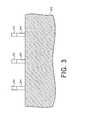
- an exemplary wafer portion 200is illustrated that includes a hardmask blocking layer 204 and a hardmask cap layer 202 .
- the wafer portion 200can comprise any suitable bulk semiconductor wafer, such as a silicon ⁇ 100 > wafer.
- the hardmask blocking layer 204 and hardmask cap layer 202can comprise any suitable hardmask material, such as silicon dioxide and silicon nitride, respectively.
- the next step 104is to pattern the hardmask blocking layer and the hardmask cap layer to form the fin pattern.
- Thiscan be done using any suitable process, and would typically involve the deposition and patterning of a suitable photoresist.
- the hardmask blocking layer and hardmask cap layercan then be patterned selective to the developed photoresist with a reactive ion etch (RIE).
- RIEreactive ion etch
- the patterned hardmask layerswill then be used to pattern the underlying semiconductor substrate during a silicon RIE to define the fins that will be used to form the finFET devices. As such, the length and width of the patterning would be determined by the desired fin size for the particular application.
- the wafer portion 200is illustrated after the hardmask blocking layer 204 and the hardmask cap layer 202 have been patterned.
- the next step 106is to form a height control layer in the semiconductor wafer.
- the next step 108is to pattern the semiconductor wafer to form the fins using the height control layer to control fin height.
- the layercan comprise the implantation of a heavy ion that damages the substrate to a desired depth and thus changes the etch rate of the damaged substrate relative to that of the undamaged substrate. This allows for improved height control during fin patterning by minimizing the effects of etch rate variations.
- the height control layercan comprise the formation of a marker layer at a desired depth. During fin patterning, the elements of the marker layer are monitored for to provide precise detection of when desired fin height is reached. Both techniques thus provide for improved fin height control, allowing fins to be reliably formed from bulk semiconductor wafers.
- the height control layercomprises an ion implant that damages the substrate
- any suitable ioncan be used that sufficiently damages the exposed portion of the semiconductor substrate to change the etch rate of the damaged substrate relative to that of the undamaged substrate.
- a As ion implantcan be used to damage the semiconductor wafer.
- Other suitable ionswould include germanium, cesium, antimony or other heavy ion.
- the energy of the implantis then selected to drive the damage to the desired depth of the fin. For example, to create a fin height of approximately 800 angstroms, we would use an As implant of 140 keV and a dose of 1 ⁇ 10e 16 /cm 2 .
- the damaged portioncan be etched faster than the undamaged portion, and a timed etch is more likely to result in a consistent depth of etch. Stated another way, the undamaged portion etches slower than the damaged portion and in a timed etch the overetch in the undamaged area is minimized. Thus, the ion implant improves the height control of the resulting fins.
- the height control layercomprises a marker layer
- detection of the marker ionindicates when the desired depth has been reached during the etch process.
- the marker layercan comprise any suitable species, such as oxygen, hydrogen or germanium.
- the marker layercan be formed by implanting the marker species (such as Ge) into the substrate.
- the marker layercan be formed by depositing the species on the substrate, and forming an additional semiconductor substrate layer over the deposited marker layer. The fins would then be etched from the layer on top of the marker layer.
- the marker speciesis monitored for while the semiconductor substrate layer is etched to define the fin.
- the marker speciesis detected the etch is stopped as the presence of the species indicates that the desired depth has been reached.
- the presence of the marker layer specieshelps determine when the etch process should be stopped, and thus results in a consistent depth of etch.
- the marker layercould be a SiGe layer between 800-1000 angstroms thick with a Ge concentration between 25%-50%.
- both techniquesthus provide for improved fin height control, allowing fins of consistent height to be reliably formed from bulk semiconductor wafers.
- the etch chemistrieswould be selected to be compatible with the type of height control layer and to be selective to the hardmask cap layer that is used to define the fin pattern.
- the wafer portion 200is illustrated after the formation of a height control layer, and after the semiconductor substrate has been patterned to form fins 210 . Again, because a height control layer was used the height of fins will have improved uniformity from wafer to wafer.
- cap layerit will be desirable to remove the cap layer at this point. This could be done using any suitable technique, such as a wet or dry etch that is selective to underlying hardmask and exposed silicon.
- the underlying hardmask blocking layeris thus left, and will be used to protect the fins in future process.
- the cap layercan be left in place to further protect the fin during future processing.
- the next step 110is to damage the substrate between the fins.
- the damage to the substrateis meant to increase the oxidation rate of the substrate between the fins relative to the oxidation rate of the fins themselves.
- One method of damaging the substrateis to implant a suitable element into the substrate between the fins. This implant is suitably done perpendicular to the surface of the substrate and thus the blocking hardmask layer prevents the implant from directly damaging the fins, although some straggle may occur. Any suitable implant can be used to damage the substrate, although it is generally preferable to chose a heavy ion that will best damage the substrate and thus increase the oxidation rate of the substrate.
- implanting Asat a dose between approximately 1 ⁇ 10e 16 /cm 2 and 1 ⁇ 10e 17 /cm 2 and at an energy of approximately 40-60 keV is a suitable choice.
- Other suitable implant speciesinclude cesium, oxygen and germanium.
- An alternative method of selectively damaging the semiconductor substrateis via an anodic reaction selective to a p-type implant.
- a p-type ionis implanted into the semiconductor substrate between the fins.
- the p-type implantcan comprise any suitable species, such as boron.
- the blocking hardmask layerprevents the p-type implant from directly damaging the fins.
- the substrateis annealed.
- the implanted regionsare then exposed to a chemical etchant such as HF/alcohol and an anodic reaction occurs. This damages the implanted regions. Specifically, the anodic reaction makes the implanted regions become porous.
- the amount of damagecan be controlled by the density and energy of the p-type implant, the HF concentration and the HF/alcohol mixture, as well as reaction current density and time.
- the damaged areaagain has an increased oxidation rate, and thus will result in differential oxide thickness between the substrate and the fins.
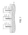
- the wafer portion 200is illustrated after the hardmask cap layer 202 has been removed and a damaging process performed to create damaged portions 212 of the substrate. Because the fins are protected by the remaining hardmask blocking layer 204 , and because the implant is primarily vertical, the damaged portions 212 of the semiconductor substrate will be concentrated in the areas between the fins.
- the next step 112is to oxidize the damaged areas of the wafer.
- Thiscan be done using any suitable oxidation process.
- the damaged areas of the waferoxidize at a much greater rate than the undamaged areas.
- oxidewill form more rapidly and more deeply in areas between the fins than on the fins themselves.
- the ratio of the two oxidation ratesis approximately 5:1. This generates an oxide of sufficient thickness between the fins to isolate the fins from each other without completely oxidizing the fin away. Additionally, the growth of oxidation under the fins further isolates the fins.
- the growth of oxidation under the finswill result in improved isolation between the source and drains of the transistors themselves. Without this isolation current can potentially flow under the fins between the source and the drain as this area may not be completely controlled by the gates of the transistor. It should be noted that the oxide grown under the fin does not necessarily need to completely extend under the fin to provide sufficient isolation between the source and drain of the transistor, although in some cases it would be desirable.
- Another aspect of this stepis that the growth of oxide on the sidewalls of the fins serves to narrow the width of the remaining semiconductor material in the fins. Narrowing of the fin can improve the performance of the transistor by improving the current control provided by the gate. It should be noted that in many cases it is desirable for the fin to be narrower than can be accurately patterned using traditional lithography. For this reason, it will be desirable in many cases to use image enhancement techniques such as sidewall image transfer to define the width of the fin. The embodiments of the invention thus provide additional advantage by further narrowing the width of the fin during formation of the isolation between the fins without completely oxidizing the fin away.
- the wafer portion 200is illustrated after the oxidation has formed isolation 214 between the fins 210 . Additionally, the oxidation has formed oxide 216 on the sidewalls of the fins 210 . Because the substrate areas between the fins were damaged before oxidation, the rate of oxide growth between the fins is much greater than in other areas, such as on the sidewalls of the fins. Additionally, the formation of oxide 216 on the fins 210 serves to further narrow the width of the fins.
- next step 114is to remove unwanted oxide and complete the finFET devices. Because the oxide formed on the sidewalls of the fin is much thinner than the oxide formed between the fins, it can be removed from the sidewalls while leaving sufficient isolation oxide between the fins. Furthermore, the formation of oxide on the sidewall of the fins further narrows the width of the fins themselves.
- the finFETscan then be completed.
- the described methodscan be applied to any type of finFET manufacturing process. A short description of an exemplary process will now be given, but those skilled in the art will recognize that other suitable processes could be used.
- the first step in the exemplary processwould be to dope the fins Typically, this may include an ion implantation into the fins so as to form P-well structures and Nâ ⁇ ” well structures.
- P-well structures and Nâ ⁇ ” well structuresare formed to allow the integration of NFETs and PFETs in a common substrate.
- P, As and Sbfor example, are well suited for PFET wells.
- B, In and Gafor example, are well suited for NFET wells.
- Ion implantationis typically designed to achieve a concentration of between 1 ⁇ 10 17 cm ⁇ 3 to 5 ⁇ 10 18 cm ⁇ 3 for example.
- ion implantationmay comprise an angled implant into exposed opposing vertical sidewalls of semiconductor layer, and would serve to properly dope the fins.
- gate stacksThis can comprise forming gate insulator layers on opposing vertical sidewalls and opposing end walls of the fins.
- Gate insulator layersmay be formed by thermal oxidation, typically at 750-800 ⁇ ° C., or alternatively, may be formed by depositing a dielectric film.
- gate insulator layersmay be SiO 2 , a nitrided oxide material, a high-K dielectric material, or combinations thereof, as known in the art.
- Gate conductor layermay be any suitable conducting material, typically a polycrystalline silicon material, although amorphous silicon, a combination of amorphous silicon and polysilicon, polysilicon-germanium, or any other appropriate material may be used to form gate conductor layer.
- a metal gate conductor layersuch as W, Mo, or Ta, or any other refractory metal, or alternatively, a silicided gate conductor comprising polysilicon added with Ni or Co.
- the gate conductor layeris a silicon material, it may be deposited as a doped layer (in-situ doping).
- gate conductor layeris a metal layer
- such layersmay be deposited using physical vapor or chemical vapor deposition methods or any other technique known in the art. In this manner, gate structures are formed adjacent to oxide layers formed on opposing vertical sidewalls of the fins formed by semiconductor layer portions.
- gate conductor layer and gate insulator layerThis would typically be accomplished by depositing and patterning a hardmask film.
- hard mask film materialmay be SiO 2 or Si 3 N 4 .
- gate conductor layermay be patterned and structured using well known photolithography and etching techniques to form the gate stack, i.e, using hardmask film caps as an etch mask during a directional etching of gate conductor layer. This involves selectively removing portions of gate conductor layer down to the isolation, but does not remove the portions of semiconductor layer forming the fins that are protected by hardmask film. Therefore, the fins may extend beyond the gate stack.
- the patterning and structuringalso leaves portions of gate conductor layer, which define the gate structures adjacent the fin bodies.
- the next stepis to dope the exposed portion of the fins with source/drain implants.
- Formation of the source/drain regionsmay be accomplished using any of the variety of methods that have been developed to form source/drain regions and that are tailored for specific performance requirements. There are many such methods for forming source/drain regions having various levels of complexity.
- lightly doped source/drain regions or other source/drain regionsmay be formed.
- NFETstypically P, As, or Sb for example is used for the source/drain implants in the range of 1 to 5 keV and a dose of 5 ⁇ 10 14 to 2 ⁇ 10 15 cm ⁇ 3 .
- PFETstypically B, In, or Ga for example is used for the source/drain implants in the range of 0.5 to 3 keV and dose of 5 ⁇ 10 14 to 2 ⁇ 10 15 cm ⁇ 3 .
- extension and halo implantsmay be formed that improve Short Channel Effects (SCE).
- SCEShort Channel Effects
- NFETstypically B, In, or Ga may be used for the halo implants with energies in the range of 5 to 15 keV and a dose of 1 ⁇ 10 13 to 8 ⁇ 10 13 cm ⁇ 3 .
- P, As, or Sbmay be used for the halos, with energies from 20 to 45 keV and dose of 1 ⁇ 10 13 to 8 ⁇ 10 13 cm ⁇ 3 .
- a dielectricmay be deposited and planarized typically using a CMP process.
- Contact holesmay then be structured and etched using an anisotropic process (e.g. RIE) or the like.
- the contact holesmay be filled using any conducting material, such as doped polysilicon, silicide (e.g. WSi), metals (e.g. Au, Al, Mo, W, Ta, Ti, Cu, or ITO (indium-tin oxide)), or the like, being deposited by evaporation, sputtering, or other known techniques, thereby forming S/D contacts.
- the first metal layermay be deposited and structured using a RIE process or the like.
- the structuring of the first metal layermay be done following a damacene process flow.
- Gate insulator layers 220are formed on each side of the fins 210 and opposing end walls of the fins.
- Gates 222are formed overlying gate insulator layers 220 and hard mask film 224 .
- gate conductor layer 222 portionsis continuous across both sides of the fin, but in other embodiments, the gate conductor layer is divided into two portions.
- CMOS FinFETs on the same substrate utilizing various crystal planes for FET current channels according to the present inventionmay be used in many different kinds of circuits, such as high performance logic, low power logic or high density memory devices, including high density multi-gigabit DRAMs.
- the CMOS FinFETsmay readily be combined with other elements, such as for example capacitors, resistors, diodes, memory cells and so forth.
- the present inventionthus provides a device structure and method for forming fin Field Effect Transistors (FETs) that overcomes many of the disadvantages of the prior art. Specifically, the method facilitates the formation of finFET devices from bulk semiconductor wafers with improved fin height control. Additionally, the method provides the ability to form finFETs from bulk silicon while providing isolation between fins and between the source and drain region of individual finFETs.
- the device structure and methods of the present inventionthus provide the advantages of reliable and consistent finFET fabrication while using cost-effective bulk wafers.
- the embodiments and examples set forth hereinwere presented in order to best explain the present invention and its practical application and to thereby enable those of ordinary skill in the art to make and use the invention.
Landscapes
- Thin Film Transistor (AREA)
- Metal-Oxide And Bipolar Metal-Oxide Semiconductor Integrated Circuits (AREA)
- Insulated Gate Type Field-Effect Transistor (AREA)
- Bipolar Transistors (AREA)
- Element Separation (AREA)
- Junction Field-Effect Transistors (AREA)
Abstract
Description
Claims (18)
Priority Applications (11)
| Application Number | Priority Date | Filing Date | Title |
|---|---|---|---|
| US10/063,994US6642090B1 (en) | 2002-06-03 | 2002-06-03 | Fin FET devices from bulk semiconductor and method for forming |
| TW092114901ATWI235457B (en) | 2002-06-03 | 2003-06-02 | Fin FET devices from bulk semiconductor and method for forming |
| DE60336237TDE60336237D1 (en) | 2002-06-03 | 2003-06-03 | METHOD FOR PRODUCING FINFET COMPONENTS FROM BULK SEMICONDUCTOR |
| PCT/US2003/017269WO2003103019A2 (en) | 2002-06-03 | 2003-06-03 | Fin fet devices from bulk semiconductor and method for forming |
| CNB038111691ACN1296991C (en) | 2002-06-03 | 2003-06-03 | Bulk semiconductor fin FET device and method of forming the same |
| EP03736783AEP1532659B1 (en) | 2002-06-03 | 2003-06-03 | Methods for forming fin fet devices from bulk semiconductor |
| AT03736783TATE500610T1 (en) | 2002-06-03 | 2003-06-03 | METHOD FOR PRODUCING FINFET COMPONENTS FROM BULK SEMICONDUCTOR |
| AU2003237320AAU2003237320A1 (en) | 2002-06-03 | 2003-06-03 | Fin fet devices from bulk semiconductor and method for forming |
| JP2004510008AJP4425130B2 (en) | 2002-06-03 | 2003-06-03 | Manufacturing method of fin-type field effect transistor |
| KR1020047017562AKR100702553B1 (en) | 2002-06-03 | 2003-06-03 | NiFFT device formed from bulk semiconductor and method of manufacturing same |
| IL16554604AIL165546A0 (en) | 2002-06-03 | 2004-12-05 | Fin fet devices from bulk semiconductor and methodfor forming |
Applications Claiming Priority (1)
| Application Number | Priority Date | Filing Date | Title |
|---|---|---|---|
| US10/063,994US6642090B1 (en) | 2002-06-03 | 2002-06-03 | Fin FET devices from bulk semiconductor and method for forming |
Publications (1)
| Publication Number | Publication Date |
|---|---|
| US6642090B1true US6642090B1 (en) | 2003-11-04 |
Family
ID=29268594
Family Applications (1)
| Application Number | Title | Priority Date | Filing Date |
|---|---|---|---|
| US10/063,994Expired - LifetimeUS6642090B1 (en) | 2002-06-03 | 2002-06-03 | Fin FET devices from bulk semiconductor and method for forming |
Country Status (11)
| Country | Link |
|---|---|
| US (1) | US6642090B1 (en) |
| EP (1) | EP1532659B1 (en) |
| JP (1) | JP4425130B2 (en) |
| KR (1) | KR100702553B1 (en) |
| CN (1) | CN1296991C (en) |
| AT (1) | ATE500610T1 (en) |
| AU (1) | AU2003237320A1 (en) |
| DE (1) | DE60336237D1 (en) |
| IL (1) | IL165546A0 (en) |
| TW (1) | TWI235457B (en) |
| WO (1) | WO2003103019A2 (en) |
Cited By (234)
| Publication number | Priority date | Publication date | Assignee | Title |
|---|---|---|---|---|
| US20040038464A1 (en)* | 2001-12-04 | 2004-02-26 | Fried David M. | Multiple-plane FinFET CMOS |
| US6720619B1 (en)* | 2002-12-13 | 2004-04-13 | Taiwan Semiconductor Manufacturing Company, Ltd. | Semiconductor-on-insulator chip incorporating partially-depleted, fully-depleted, and multiple-gate devices |
| US6756643B1 (en)* | 2003-06-12 | 2004-06-29 | Advanced Micro Devices, Inc. | Dual silicon layer for chemical mechanical polishing planarization |
| US6787854B1 (en)* | 2003-03-12 | 2004-09-07 | Advanced Micro Devices, Inc. | Method for forming a fin in a finFET device |
| US6787476B1 (en)* | 2003-08-04 | 2004-09-07 | Advanced Micro Devices, Inc. | Etch stop layer for etching FinFET gate over a large topography |
| US20040197975A1 (en)* | 2003-01-23 | 2004-10-07 | Zoran Krivokapic | Narrow fin finfet |
| US6812119B1 (en)* | 2003-07-08 | 2004-11-02 | Advanced Micro Devices, Inc. | Narrow fins by oxidation in double-gate finfet |
| US20040217433A1 (en)* | 2003-04-29 | 2004-11-04 | Yee-Chia Yeo | Doping of semiconductor fin devices |
| US6815268B1 (en)* | 2002-11-22 | 2004-11-09 | Advanced Micro Devices, Inc. | Method for forming a gate in a FinFET device |
| US20040266077A1 (en)* | 2003-06-27 | 2004-12-30 | Yee-Chia Yeo | Structure and method for forming the gate electrode in a multiple-gate transistor |
| US20050023633A1 (en)* | 2003-08-01 | 2005-02-03 | Yee-Chia Yeo | Semiconductor-on-insulator SRAM configured using partially-depleted and fully-depleted transistors |
| US20050056888A1 (en)* | 2003-09-16 | 2005-03-17 | Jae-Man Youn | Double gate field effect transistor and method of manufacturing the same |
| US6872647B1 (en)* | 2003-05-06 | 2005-03-29 | Advanced Micro Devices, Inc. | Method for forming multiple fins in a semiconductor device |
| US20050104091A1 (en)* | 2003-11-04 | 2005-05-19 | Tabery Cyrus E. | Self aligned damascene gate |
| US20050116218A1 (en)* | 2003-11-24 | 2005-06-02 | Samsung Electronics Co., Ltd. | Non-planar transistor having germanium channel region and method of manufacturing the same |
| US20050121706A1 (en)* | 2003-02-20 | 2005-06-09 | Hao-Yu Chen | Semiconductor nano-rod devices |
| US20050136617A1 (en)* | 2003-12-03 | 2005-06-23 | Young-Chul Jang | MOS transistor having protruded-shape channel and method of fabricating the same |
| US20050153485A1 (en)* | 2004-01-12 | 2005-07-14 | Ahmed Shibly S. | Narrow-body damascene tri-gate FinFET |
| US20050153490A1 (en)* | 2003-12-16 | 2005-07-14 | Jae-Man Yoon | Method of forming fin field effect transistor |
| US20050156202A1 (en)* | 2004-01-17 | 2005-07-21 | Hwa-Sung Rhee | At least penta-sided-channel type of FinFET transistor |
| US20050173768A1 (en)* | 2004-02-10 | 2005-08-11 | Samsung Electronics Co., Ltd. | Fin fet structure |
| US20050179030A1 (en)* | 2004-02-13 | 2005-08-18 | Hyeoung-Won Seo | Field effect transistor device with channel fin structure and method of fabricating the same |
| US20050186746A1 (en)* | 2004-02-23 | 2005-08-25 | Chul Lee | Method of manufacturing a fin field effect transistor |
| US20050184283A1 (en)* | 2004-02-20 | 2005-08-25 | Shigenobu Maeda | Semiconductor device having a triple gate transistor and method for manufacturing the same |
| US20050191795A1 (en)* | 2004-03-01 | 2005-09-01 | Dureseti Chidambarrao | Method of manufacture of FinFET devices with T-shaped fins and devices manufactured thereby |
| US20050194616A1 (en)* | 2004-03-04 | 2005-09-08 | Jae-Man Yoon | Transistor and method of forming the same |
| US20050202608A1 (en)* | 2004-03-15 | 2005-09-15 | International Business Machines Corporation | Locally thinned fins |
| US6947275B1 (en) | 2004-10-18 | 2005-09-20 | International Business Machines Corporation | Fin capacitor |
| US20050233565A1 (en)* | 2004-04-15 | 2005-10-20 | International Business Machines Corporation | Methods for manufacturing a finfet using a conventional wafer and apparatus manufactured therefrom |
| US20050237850A1 (en)* | 2003-10-02 | 2005-10-27 | Suman Datta | Method and apparatus for improving stability of a 6T CMOS SRAM cell |
| US20050239242A1 (en)* | 2004-04-23 | 2005-10-27 | International Business Machines Corporation | structure and method of manufacturing a finFet device having stacked fins |
| US20050239254A1 (en)* | 2004-04-24 | 2005-10-27 | Taiwan Semiconductor Manufacturing Co., Ltd. | Quasi-plannar and FinFET-like transistors on bulk silicon |
| US6960509B1 (en)* | 2004-06-30 | 2005-11-01 | Freescale Semiconductor, Inc. | Method of fabricating three dimensional gate structure using oxygen diffusion |
| US20050250279A1 (en)* | 2004-03-05 | 2005-11-10 | Yong-Hoon Son | Methods of forming semiconductor devices having buried oxide patterns and devices related thereto |
| US20050255643A1 (en)* | 2004-05-14 | 2005-11-17 | Samsung Electronics Co., Ltd. | Method of forming fin field effect transistor using damascene process |
| US20050255656A1 (en)* | 2004-05-17 | 2005-11-17 | Hee-Soo Kang | Field effect transistor (FET) devices and methods of manufacturing FET devices |
| US6967175B1 (en)* | 2003-12-04 | 2005-11-22 | Advanced Micro Devices, Inc. | Damascene gate semiconductor processing with local thinning of channel region |
| US20050263795A1 (en)* | 2004-05-25 | 2005-12-01 | Jeong-Dong Choi | Semiconductor device having a channel layer and method of manufacturing the same |
| US20050275010A1 (en)* | 2004-06-10 | 2005-12-15 | Hung-Wei Chen | Semiconductor nano-wire devices and methods of fabrication |
| US20060022262A1 (en)* | 2004-07-30 | 2006-02-02 | Jae-Man Yoon | Semiconductor device having a fin structure and method of manufacturing the same |
| US20060043472A1 (en)* | 2004-08-24 | 2006-03-02 | Hongmei Wang | High density access transistor having increased channel width and methods of fabricating such devices |
| EP1566844A3 (en)* | 2004-02-20 | 2006-04-05 | Samsung Electronics Co., Ltd. | Multi-gate transistor and method for manufacturing the same |
| US20060084247A1 (en)* | 2004-10-20 | 2006-04-20 | Kaiping Liu | Transistors, integrated circuits, systems, and processes of manufacture with improved work function modulation |
| US20060088967A1 (en)* | 2004-10-26 | 2006-04-27 | Nanya Technology Corporation | Finfet transistor process |
| US20060118876A1 (en)* | 2004-12-03 | 2006-06-08 | Samsung Electronics Co., Ltd. | Fin field effect transistor and method of manufacturing the same |
| US20060128071A1 (en)* | 2002-12-20 | 2006-06-15 | Rankin Jed H | Integrated antifuse structure for finfet and cmos devices |
| WO2006070310A1 (en)* | 2004-12-28 | 2006-07-06 | Koninklijke Philips Electronics N.V. | Method for the manufacture of a semiconductor device and a semiconductor device obtained through it |
| US20060154426A1 (en)* | 2005-01-13 | 2006-07-13 | International Business Machines Corporation | Finfets with long gate length at high density |
| US20060160302A1 (en)* | 2004-12-10 | 2006-07-20 | Kim Sung-Min | Method of fabricating a fin field effect transistor having a plurality of protruding channels |
| US7084018B1 (en)* | 2004-05-05 | 2006-08-01 | Advanced Micro Devices, Inc. | Sacrificial oxide for minimizing box undercut in damascene FinFET |
| US7101763B1 (en) | 2005-05-17 | 2006-09-05 | International Business Machines Corporation | Low capacitance junction-isolation for bulk FinFET technology |
| US20060214233A1 (en)* | 2005-03-22 | 2006-09-28 | Ananthanarayanan Hari P | FinFET semiconductor device |
| US20070010049A1 (en)* | 2005-06-21 | 2007-01-11 | International Business Machines Corporation | Thermal dissipation structures for finfets |
| US20070026629A1 (en)* | 2005-07-29 | 2007-02-01 | Taiwan Semiconductor Manufacturing Company, Ltd. | Novel structure for a multiple-gate FET device and a method for its fabrication |
| US20070034925A1 (en)* | 2003-06-30 | 2007-02-15 | Deok-Hyung Lee | Fin-field effect transistors (Fin-FETs) having protection layers |
| KR100714775B1 (en)* | 2004-06-22 | 2007-05-04 | 샤프 가부시키가이샤 | Field effect transistor and fabrication method thereof |
| US20070102756A1 (en)* | 2005-11-10 | 2007-05-10 | Bohumil Lojek | FinFET transistor fabricated in bulk semiconducting material |
| US20070108528A1 (en)* | 2005-11-15 | 2007-05-17 | International Business Machines Corporation | Sram cell |
| US20070131983A1 (en)* | 2005-12-13 | 2007-06-14 | Intel Corporation | Tri-gate integration with embedded floating body memory cell using a high-K dual metal gate |
| US20070134884A1 (en)* | 2005-12-14 | 2007-06-14 | Samsung Electronics Co., Ltd. | Isolation method of defining active fins, method of fabricating semiconductor device using the same and semiconductor device fabricated thereby |
| US20070134878A1 (en)* | 2005-12-09 | 2007-06-14 | Intel Corporation | Non-planar microelectronic device having isolation element to mitigate fringe effects and method to fabricate same |
| KR100728957B1 (en)* | 2005-06-30 | 2007-06-15 | 주식회사 하이닉스반도체 | Protruding transistor manufacturing method |
| US20070138514A1 (en)* | 2005-12-21 | 2007-06-21 | Chang Peter L | Integration of planar and tri-gate devices on the same substrate |
| US20070148926A1 (en)* | 2005-12-28 | 2007-06-28 | Intel Corporation | Dual halo implant for improving short channel effect in three-dimensional tri-gate transistors |
| US7241653B2 (en) | 2003-06-27 | 2007-07-10 | Intel Corporation | Nonplanar device with stress incorporation layer and method of fabrication |
| CN1326217C (en)* | 2003-12-09 | 2007-07-11 | 国际商业机器公司 | Pull-back method of forming fins in FinFET |
| US20070166900A1 (en)* | 2006-01-17 | 2007-07-19 | International Business Machines Corporation | Device fabrication by anisotropic wet etch |
| US20070205459A1 (en)* | 2006-03-02 | 2007-09-06 | Cho Eun-Suk | Nonvolatile memory devices and methods of forming the same |
| US20070221992A1 (en)* | 2003-09-15 | 2007-09-27 | Seliskar John J | Castellated gate MOSFET device capable of fully-depleted operation |
| US20070231997A1 (en)* | 2006-03-31 | 2007-10-04 | Doyle Brian S | Stacked multi-gate transistor design and method of fabrication |
| US20070235763A1 (en)* | 2006-03-29 | 2007-10-11 | Doyle Brian S | Substrate band gap engineered multi-gate pMOS devices |
| US7291564B1 (en)* | 2006-04-28 | 2007-11-06 | Hewlett-Packard Development Company, L.P. | Method and structure for facilitating etching |
| US20070264762A1 (en)* | 2003-11-04 | 2007-11-15 | Yee-Chia Yeo | Semiconductor-on-insulator SRAM configured using partially-depleted and fully-depleted transistors |
| US20070269950A1 (en)* | 2005-02-24 | 2007-11-22 | Anderson Brent A | Double gate isolation |
| US20070284583A1 (en)* | 2003-10-03 | 2007-12-13 | Kabushiki Kaisha Toshiba | Semiconductor device and method of manufacturing the same |
| US20080002477A1 (en)* | 2005-09-05 | 2008-01-03 | Macronix International Co., Ltd. | Method for manufacturing memory cell |
| CN100367515C (en)* | 2003-11-20 | 2008-02-06 | 国际商业机器公司 | Field effect transistor, integrated circuit and method of forming integrated circuit |
| US20080048265A1 (en)* | 2005-08-25 | 2008-02-28 | International Business Machines Corporation | Semiconductor structures integrating damascene-body finfet's and planar devices on a common substrate and methods for forming such semiconductor structures |
| US20080057712A1 (en)* | 2006-06-16 | 2008-03-06 | Synopsys, Inc. | Method For Achieving Uniform Etch Depth Using Ion Implantation And A timed Etch |
| US20080054361A1 (en)* | 2006-08-30 | 2008-03-06 | Infineon Technologies Ag | Method and apparatus for reducing flicker noise in a semiconductor device |
| CN100375252C (en)* | 2004-04-28 | 2008-03-12 | 国际商业机器公司 | Fin field effect transistor semiconductor structure and manufacturing method thereof |
| US20080061371A1 (en)* | 2004-05-17 | 2008-03-13 | Samsung Electronics Co., Ltd. | Field effect transistor (fet) devices and methods of manufacturing fet devices |
| US7348284B2 (en) | 2004-08-10 | 2008-03-25 | Intel Corporation | Non-planar pMOS structure with a strained channel region and an integrated strained CMOS flow |
| US7358142B2 (en) | 2004-02-02 | 2008-04-15 | Samsung Electronics Co., Ltd. | Method for forming a FinFET by a damascene process |
| US7361958B2 (en) | 2004-09-30 | 2008-04-22 | Intel Corporation | Nonplanar transistors with metal gate electrodes |
| US20080097346A1 (en)* | 2006-09-19 | 2008-04-24 | Alcon, Inc. | Trocar cannula |
| US20080099830A1 (en)* | 2006-11-01 | 2008-05-01 | Macronix International Co., Ltd. | Cylindrical channel charge trapping devices with effectively high coupling ratios |
| US20080119020A1 (en)* | 2006-11-17 | 2008-05-22 | Micron Technology, Inc. | Methods of forming a field effect transistors, pluralities of field effect transistors, and DRAM circuitry comprising a plurality of individual memory cells |
| US20080121998A1 (en)* | 2006-09-15 | 2008-05-29 | Kavalieros Jack T | Apparatus and method for selectively recessing spacers on multi-gate devices |
| US7396711B2 (en) | 2005-12-27 | 2008-07-08 | Intel Corporation | Method of fabricating a multi-cornered film |
| US20080176363A1 (en)* | 2005-07-27 | 2008-07-24 | Anderson Brent A | Virtual body-contacted trigate |
| US20080188080A1 (en)* | 2005-09-14 | 2008-08-07 | International Business Machines Corporation | Mandrel/trim alignment in sit processing |
| US20080206934A1 (en)* | 2007-02-23 | 2008-08-28 | Jones Robert E | Forming semiconductor fins using a sacrificial fin |
| US7425500B2 (en) | 2006-03-31 | 2008-09-16 | Intel Corporation | Uniform silicide metal on epitaxially grown source and drain regions of three-dimensional transistors |
| US20080230852A1 (en)* | 2007-03-06 | 2008-09-25 | Chen-Hua Yu | Fabrication of FinFETs with multiple fin heights |
| US20080251849A1 (en)* | 2004-03-19 | 2008-10-16 | Shigeharu Yamagami | Semiconductor Device and Method for Manufacturing Same |
| US20080251839A1 (en)* | 2007-04-12 | 2008-10-16 | Hynix Semiconductor Inc. | Semiconductor device and method for fabricating the same |
| US20080265338A1 (en)* | 2007-04-27 | 2008-10-30 | Chen-Hua Yu | Semiconductor Device Having Multiple Fin Heights |
| US7449373B2 (en) | 2006-03-31 | 2008-11-11 | Intel Corporation | Method of ion implanting for tri-gate devices |
| US7456476B2 (en) | 2003-06-27 | 2008-11-25 | Intel Corporation | Nonplanar semiconductor device with partially or fully wrapped around gate electrode and methods of fabrication |
| US7479421B2 (en) | 2005-09-28 | 2009-01-20 | Intel Corporation | Process for integrating planar and non-planar CMOS transistors on a bulk substrate and article made thereby |
| US20090040829A1 (en)* | 2007-08-09 | 2009-02-12 | Macronix International Co., Ltd. | Lateral pocket implant charge trapping devices |
| CN100470841C (en)* | 2005-03-30 | 2009-03-18 | 台湾积体电路制造股份有限公司 | Quasi-planar and fin-like field effect transistor elements and methods of making same |
| WO2009044236A1 (en)* | 2007-10-03 | 2009-04-09 | Freescale Semiconductor, Inc. | Method of forming an inverted t shaped channel structure for an inverted t channel field effect transistor device |
| US7518196B2 (en) | 2005-02-23 | 2009-04-14 | Intel Corporation | Field effect transistor with narrow bandgap source and drain regions and method of fabrication |
| US20090101975A1 (en)* | 2005-02-21 | 2009-04-23 | Infineon Technologies Ag | Integrated Circuit Arrangement Comprising a Field Effect Transistor, Especially a Tunnel Field Effect Transistor |
| US7525160B2 (en) | 2005-12-27 | 2009-04-28 | Intel Corporation | Multigate device with recessed strain regions |
| US20090124097A1 (en)* | 2007-11-09 | 2009-05-14 | International Business Machines Corporation | Method of forming narrow fins in finfet devices with reduced spacing therebetween |
| US7547637B2 (en) | 2005-06-21 | 2009-06-16 | Intel Corporation | Methods for patterning a semiconductor film |
| US7550333B2 (en) | 2004-10-25 | 2009-06-23 | Intel Corporation | Nonplanar device with thinned lower body portion and method of fabrication |
| US7566619B2 (en) | 2004-04-27 | 2009-07-28 | Samsung Electronics Co., Ltd. | Methods of forming integrated circuit devices having field effect transistors of different types in different device regions |
| US7579280B2 (en) | 2004-06-01 | 2009-08-25 | Intel Corporation | Method of patterning a film |
| US20090256207A1 (en)* | 2008-04-14 | 2009-10-15 | International Business Machines Corporation | Finfet devices from bulk semiconductor and methods for manufacturing the same |
| US7700470B2 (en) | 2006-09-22 | 2010-04-20 | Intel Corporation | Selective anisotropic wet etching of workfunction metal for semiconductor devices |
| US7736956B2 (en) | 2005-08-17 | 2010-06-15 | Intel Corporation | Lateral undercut of metal gate in SOI device |
| US20100155801A1 (en)* | 2008-12-22 | 2010-06-24 | Doyle Brian S | Integrated circuit, 1T-1C embedded memory cell containing same, and method of manufacturing 1T-1C memory cell for embedded memory application |
| US20100163945A1 (en)* | 2008-12-30 | 2010-07-01 | Kavalieros Jack T | Embedded memory cell and method of manufacturing same |
| US20100176438A1 (en)* | 2009-01-15 | 2010-07-15 | Macronix International Co., Ltd. | Depletion-mode charge-trapping flash device |
| US7781771B2 (en) | 2004-03-31 | 2010-08-24 | Intel Corporation | Bulk non-planar transistor having strained enhanced mobility and methods of fabrication |
| US20100214863A1 (en)* | 2009-02-23 | 2010-08-26 | Taiwan Semiconductor Manufacturing Company, Ltd. | Memory power gating circuit and methods |
| US20100232203A1 (en)* | 2009-03-16 | 2010-09-16 | Taiwan Semiconductor Manufacturing Company, Ltd. | Electrical anti-fuse and related applications |
| US20100244144A1 (en)* | 2009-03-31 | 2010-09-30 | Taiwan Semiconductor Manufacturing Company, Ltd. | Electrical fuse and related applications |
| US20100248454A1 (en)* | 2009-03-27 | 2010-09-30 | Advanced Micro Devices, Inc. | Method of forming fin structures using a sacrificial etch stop layer on bulk semiconductor material |
| US7811890B2 (en)* | 2006-10-11 | 2010-10-12 | Macronix International Co., Ltd. | Vertical channel transistor structure and manufacturing method thereof |
| US20100258870A1 (en)* | 2009-04-14 | 2010-10-14 | Taiwan Semiconductor Manufacturing Company, Ltd. | Finfets and methods for forming the same |
| US20100264472A1 (en)* | 2003-10-15 | 2010-10-21 | Infineon Technologies Ag | Patterning method, and field effect transistors |
| US7855105B1 (en)* | 2009-06-18 | 2010-12-21 | International Business Machines Corporation | Planar and non-planar CMOS devices with multiple tuned threshold voltages |
| US7859053B2 (en) | 2004-09-29 | 2010-12-28 | Intel Corporation | Independently accessed double-gate and tri-gate transistors in same process flow |
| US7867860B2 (en) | 2003-07-25 | 2011-01-11 | Taiwan Semiconductor Manufacturing Company, Ltd. | Strained channel transistor formation |
| US20110006390A1 (en)* | 2009-07-08 | 2011-01-13 | Taiwan Semiconductor Manufacturing Company, Ltd. | Sti structure and method of forming bottom void in same |
| US20110021010A1 (en)* | 2009-07-27 | 2011-01-27 | International Business Machines Corporation | Method for double pattern density |
| US7879675B2 (en) | 2005-03-14 | 2011-02-01 | Intel Corporation | Field effect transistor with metal source/drain regions |
| US20110027948A1 (en)* | 2009-07-31 | 2011-02-03 | International Business Machines Corporation | Method for manufacturing a finfet device |
| US20110024794A1 (en)* | 2009-07-31 | 2011-02-03 | Taiwan Semiconductor Manufacturing Company, Ltd. | Fin structure for high mobility multiple-gate transistor |
| US20110024804A1 (en)* | 2009-07-28 | 2011-02-03 | Taiwan Semiconductor Manufacturing Company, Ltd. | Method for forming high germanium concentration sige stressor |
| US20110045648A1 (en)* | 2009-08-20 | 2011-02-24 | Globalfoundries Inc. | Methods for fabricating bulk finfet devices having deep trench isolation |
| US7898041B2 (en) | 2005-06-30 | 2011-03-01 | Intel Corporation | Block contact architectures for nanoscale channel transistors |
| US20110049613A1 (en)* | 2009-09-01 | 2011-03-03 | Taiwan Semiconductor Manufacturing Company, Ltd. | Accumulation type finfet, circuits and fabrication method thereof |
| US7902014B2 (en) | 2005-09-28 | 2011-03-08 | Intel Corporation | CMOS devices with a single work function gate electrode and method of fabrication |
| US20110062520A1 (en)* | 2005-06-15 | 2011-03-17 | Brask Justin K | Method for fabricating transistor with thinned channel |
| US20110068431A1 (en)* | 2009-09-18 | 2011-03-24 | Globalfoundries Inc. | Semiconductor structures and methods for forming isolation between fin structures of finfet devices |
| US20110068405A1 (en)* | 2009-09-24 | 2011-03-24 | Taiwan Semiconductor Manufacturing Company, Ltd. | Fin field effect transistor |
| US7915167B2 (en) | 2004-09-29 | 2011-03-29 | Intel Corporation | Fabrication of channel wraparound gate structure for field-effect transistor |
| US20110079829A1 (en)* | 2009-10-01 | 2011-04-07 | Taiwan Semiconductor Manufacturing Company, Ltd. | Finfets and methods for forming the same |
| US20110081764A1 (en)* | 2009-10-07 | 2011-04-07 | Globalfoundries Inc. | Methods for forming isolated fin structures on bulk semiconductor material |
| US20110097867A1 (en)* | 2009-10-22 | 2011-04-28 | Taiwan Semiconductor Manufacturing Company, Ltd. | Method of controlling gate thicknesses in forming fusi gates |
| US20110143510A1 (en)* | 2009-12-15 | 2011-06-16 | Taiwan Semiconductor Manufacturing Company, Ltd. | Method of controlling gate thickness in forming finfet devices |
| US20110163313A1 (en)* | 2008-08-28 | 2011-07-07 | Memc Electronic Materials, Inc. | Bulk silicon wafer product useful in the manufacture of three dimensional multigate mosfets |
| US20110182098A1 (en)* | 2010-01-27 | 2011-07-28 | Taiwan Semiconductor Manufacturing Company, Ltd. | Integrated circuits and methods for forming the same |
| US7989280B2 (en) | 2005-11-30 | 2011-08-02 | Intel Corporation | Dielectric interface for group III-V semiconductor device |
| US20110204443A1 (en)* | 2010-02-23 | 2011-08-25 | International Business Machines Corporation | Semiconductor-on-insulator (soi) structure and method of forming the soi structure using a bulk semiconductor starting wafer |
| US20110233679A1 (en)* | 2010-03-25 | 2011-09-29 | Taiwan Semiconductor Manufacturing Company, Ltd. | Integrated circuit including finfets and methods for forming the same |
| US20110291166A1 (en)* | 2010-05-27 | 2011-12-01 | International Business Machines Corporation | Integrated circuit with finfets and mim fin capacitor |
| US8084818B2 (en) | 2004-06-30 | 2011-12-27 | Intel Corporation | High mobility tri-gate devices and methods of fabrication |
| US8187928B2 (en) | 2010-09-21 | 2012-05-29 | Taiwan Semiconductor Manufacturing Company, Ltd. | Methods of forming integrated circuits |
| US8298925B2 (en) | 2010-11-08 | 2012-10-30 | Taiwan Semiconductor Manufacturing Company, Ltd. | Mechanisms for forming ultra shallow junction |
| US20120295444A1 (en)* | 2011-05-16 | 2012-11-22 | Varian Semiconductor Equipment Associates, Inc. | Techniques for forming 3d structures |
| WO2013006612A1 (en)* | 2011-07-05 | 2013-01-10 | International Business Machines Corporation (Yt) | Bulk finfet with uniform height and bottom isolation |
| US8354320B1 (en)* | 2012-02-09 | 2013-01-15 | Globalfoundries Inc. | Methods of controlling fin height of FinFET devices by performing a directional deposition process |
| US8362566B2 (en) | 2008-06-23 | 2013-01-29 | Intel Corporation | Stress in trigate devices using complimentary gate fill materials |
| US8377779B1 (en)* | 2012-01-03 | 2013-02-19 | Taiwan Semiconductor Manufacturing Company, Ltd. | Methods of manufacturing semiconductor devices and transistors |
| US20130056826A1 (en)* | 2011-09-01 | 2013-03-07 | Taiwan Semiconductor Manufacturing Company, Ltd. | Multi-Fin Device and Method of Making Same |
| CN103000517A (en)* | 2011-09-09 | 2013-03-27 | 中芯国际集成电路制造(北京)有限公司 | Semiconductor device and manufacturing method thereof |
| US8431453B2 (en) | 2011-03-31 | 2013-04-30 | Taiwan Semiconductor Manufacturing Company, Ltd. | Plasma doping to reduce dielectric loss during removal of dummy layers in a gate structure |
| US20130113026A1 (en)* | 2011-11-03 | 2013-05-09 | Taiwan Semiconductor Manufacturing Company, Ltd. | Fin field effect transistor gate oxide |
| US8440517B2 (en) | 2010-10-13 | 2013-05-14 | Taiwan Semiconductor Manufacturing Company, Ltd. | FinFET and method of fabricating the same |
| US8460984B2 (en)* | 2011-06-09 | 2013-06-11 | GlobalFoundries, Inc. | FIN-FET device and method and integrated circuits using such |
| US8466028B2 (en) | 2011-06-30 | 2013-06-18 | Institute of Microelectronics, Chinese Academy of Sciences | Method for manufacturing multigate device |
| US20130181263A1 (en)* | 2012-01-16 | 2013-07-18 | Globalfoundries Inc. | Methods of Forming a Dielectric Cap Layer on a Metal Gate Structure |
| US8497528B2 (en) | 2010-05-06 | 2013-07-30 | Taiwan Semiconductor Manufacturing Company, Ltd. | Method for fabricating a strained structure |
| TWI409857B (en)* | 2006-01-23 | 2013-09-21 | Lam Res Corp | Fin structure formation |
| US20130285144A1 (en)* | 2006-10-02 | 2013-10-31 | SK Hynix Inc. | Dual polysilicon gate of a semiconductor device with a multi-plane channel |
| US8592915B2 (en) | 2011-01-25 | 2013-11-26 | Taiwan Semiconductor Manufacturing Company, Ltd. | Doped oxide for shallow trench isolation (STI) |
| US8597994B2 (en) | 2011-05-23 | 2013-12-03 | GlobalFoundries, Inc. | Semiconductor device and method of fabrication |
| US8603924B2 (en) | 2010-10-19 | 2013-12-10 | Taiwan Semiconductor Manufacturing Company, Ltd. | Methods of forming gate dielectric material |
| US8617945B2 (en) | 2006-08-02 | 2013-12-31 | Intel Corporation | Stacking fault and twin blocking barrier for integrating III-V on Si |
| US20140120677A1 (en)* | 2012-10-30 | 2014-05-01 | Globalfoundries Inc. | Methods of forming enhanced mobility channel regions on 3d semiconductor devices, and devices comprising same |
| US8742483B2 (en) | 2006-05-17 | 2014-06-03 | Micron Technology, Inc. | DRAM arrays |
| US8759943B2 (en)* | 2010-10-08 | 2014-06-24 | Taiwan Semiconductor Manufacturing Company, Ltd. | Transistor having notched fin structure and method of making the same |
| US8769446B2 (en) | 2010-11-12 | 2014-07-01 | Taiwan Semiconductor Manufacturing Company, Ltd. | Method and device for increasing fin device density for unaligned fins |
| US8772858B2 (en) | 2006-10-11 | 2014-07-08 | Macronix International Co., Ltd. | Vertical channel memory and manufacturing method thereof and operating method using the same |
| US20140193963A1 (en)* | 2011-05-16 | 2014-07-10 | Varian Semiconductor Equipment Associates, Inc. | Techniques For Forming 3D Structures |
| US20140191324A1 (en)* | 2013-01-08 | 2014-07-10 | International Business Machines Corporation | Methods of forming bulk finfet devices by performing a recessing process on liner materials to define different fin heights and finfet devices with such recessed liner materials |
| US8791506B2 (en) | 2006-08-28 | 2014-07-29 | Micron Technology, Inc. | Semiconductor devices, assemblies and constructions |
| US20140217506A1 (en)* | 2013-02-07 | 2014-08-07 | International Business Machines Corporation | Diode Structure and Method for FINFET Technologies |
| US20140284727A1 (en)* | 2005-07-01 | 2014-09-25 | Synopsys, Inc. | Integrated Circuit On Corrugated Substrate |
| US20140306274A1 (en)* | 2013-04-11 | 2014-10-16 | International Business Machines Corporation | SELF-ALIGNED STRUCTURE FOR BULK FinFET |
| US8896063B2 (en) | 2013-04-18 | 2014-11-25 | International Business Machines Corporation | FinFET devices containing merged epitaxial Fin-containing contact regions |
| US20140374807A1 (en)* | 2013-06-19 | 2014-12-25 | International Business Machines Corporation | METHOD OF DEVICE ISOLATION IN CLADDING Si THROUGH IN SITU DOPING |
| US8946027B2 (en) | 2012-02-07 | 2015-02-03 | International Business Machines Corporation | Replacement-gate FinFET structure and process |
| US8951850B1 (en) | 2013-08-21 | 2015-02-10 | International Business Machines Corporation | FinFET formed over dielectric |
| US20150044826A1 (en)* | 2013-08-06 | 2015-02-12 | Stmicroelectronics Sa | Method of introducing local stress in a semiconductor layer |
| US20150044827A1 (en)* | 2013-08-06 | 2015-02-12 | Stmicoelectronics Sa | Method of locally stressing a semiconductor layer |
| US8980719B2 (en) | 2010-04-28 | 2015-03-17 | Taiwan Semiconductor Manufacturing Company, Ltd. | Methods for doping fin field-effect transistors |
| US9040393B2 (en) | 2010-01-14 | 2015-05-26 | Taiwan Semiconductor Manufacturing Company, Ltd. | Method of forming semiconductor structure |
| US20150147863A1 (en)* | 2011-12-22 | 2015-05-28 | Bernhard Sell | Semiconductor device having a necked semiconductor body and method of forming semiconductor bodies of varying width |
| US9048181B2 (en) | 2010-11-08 | 2015-06-02 | Taiwan Semiconductor Manufacturing Company, Ltd. | Mechanisms for forming ultra shallow junction |
| US9059043B1 (en)* | 2014-02-11 | 2015-06-16 | International Business Machines Corporation | Fin field effect transistor with self-aligned source/drain regions |
| US9059242B2 (en) | 2012-11-27 | 2015-06-16 | International Business Machines Corporation | FinFET semiconductor device having increased gate height control |
| US9087869B2 (en) | 2013-05-23 | 2015-07-21 | International Business Machines Corporation | Bulk semiconductor fins with self-aligned shallow trench isolation structures |
| US9093376B2 (en) | 2012-10-24 | 2015-07-28 | International Business Machines Corporation | Replacement metal gate FinFET |
| US9190328B2 (en) | 2014-01-30 | 2015-11-17 | International Business Machines Corporation | Formation of fins having different heights in fin field effect transistors |
| US9190466B2 (en) | 2013-12-27 | 2015-11-17 | International Business Machines Corporation | Independent gate vertical FinFET structure |
| EP2947695A1 (en)* | 2014-05-23 | 2015-11-25 | Broadcom Corporation | Finfet with undoped body bulk |
| US9263587B1 (en)* | 2014-09-04 | 2016-02-16 | Globalfoundries Inc. | Fin device with blocking layer in channel region |
| US9263455B2 (en) | 2013-07-23 | 2016-02-16 | Micron Technology, Inc. | Methods of forming an array of conductive lines and methods of forming an array of recessed access gate lines |
| US9299924B1 (en) | 2015-06-29 | 2016-03-29 | International Business Machines Corporation | Injection pillar definition for line MRAM by a self-aligned sidewall transfer |
| US9362383B1 (en) | 2015-09-17 | 2016-06-07 | International Business Machines Corporation | Highly scaled tunnel FET with tight pitch and method to fabricate same |
| US9385123B2 (en) | 2014-05-20 | 2016-07-05 | International Business Machines Corporation | STI region for small fin pitch in FinFET devices |
| US20160211839A1 (en)* | 2013-09-27 | 2016-07-21 | Socionext Inc. | Semiconductor integrated circuit and semiconductor integrated circuit device |
| US20160218180A1 (en)* | 2015-01-27 | 2016-07-28 | Jung-Gun You | Methods for fabricating semiconductor devices having fin-shaped patterns |
| US9461147B2 (en) | 2014-11-05 | 2016-10-04 | United Microelectronics Corp. | Semiconductor structure |
| US9478641B2 (en) | 2012-08-29 | 2016-10-25 | Peking University | Method for fabricating FinFET with separated double gates on bulk silicon |
| US9508597B1 (en)* | 2015-09-18 | 2016-11-29 | Globalfoundries Inc. | 3D fin tunneling field effect transistor |
| US9515089B1 (en) | 2015-05-14 | 2016-12-06 | International Business Machines Corporation | Bulk fin formation with vertical fin sidewall profile |
| US9536986B2 (en)* | 2014-12-30 | 2017-01-03 | International Business Machines Corporation | Enriched, high mobility strained fin having bottom dielectric isolation |
| WO2017003411A1 (en) | 2015-06-27 | 2017-01-05 | Intel Corporation | Multi-height finfet device by selective oxidation |
| US9583625B2 (en)* | 2014-10-24 | 2017-02-28 | Globalfoundries Inc. | Fin structures and multi-Vt scheme based on tapered fin and method to form |
| US9590077B2 (en)* | 2015-05-14 | 2017-03-07 | International Business Machines Corporation | Local SOI fins with multiple heights |
| US9627263B1 (en) | 2015-11-30 | 2017-04-18 | International Business Machines Corporation | Stop layer through ion implantation for etch stop |
| US9691903B2 (en)* | 2015-07-07 | 2017-06-27 | Taiwan Semiconductor Manufacturing Co., Ltd. | Semiconductor device and manufacturing method thereof |
| US9691763B2 (en) | 2013-12-27 | 2017-06-27 | International Business Machines Corporation | Multi-gate FinFET semiconductor device with flexible design width |
| US9780091B2 (en)* | 2015-11-23 | 2017-10-03 | International Business Machines Corporation | Fin pitch scaling for high voltage devices and low voltage devices on the same wafer |
| US9824934B1 (en) | 2016-09-30 | 2017-11-21 | International Business Machines Corporation | Shallow trench isolation recess process flow for vertical field effect transistor fabrication |
| TWI619000B (en)* | 2016-01-27 | 2018-03-21 | 台灣積體電路製造股份有限公司 | Double transistor bandgap reference circuit body, integrated circuit and manufacturing method thereof |
| TWI624876B (en)* | 2016-02-16 | 2018-05-21 | 格羅方德半導體公司 | FINFET with notched fins and method of forming same |
| US9985030B2 (en) | 2014-04-07 | 2018-05-29 | International Business Machines Corporation | FinFET semiconductor device having integrated SiGe fin |
| US10163914B2 (en)* | 2017-03-08 | 2018-12-25 | Globalfoundries Inc. | Method of reducing fin width in FinFET SRAM array to mitigate low voltage strap bit fails |
| US10304744B1 (en)* | 2018-05-15 | 2019-05-28 | International Business Machines Corporation | Inverse tone direct print EUV lithography enabled by selective material deposition |
| CN113161352A (en)* | 2020-01-23 | 2021-07-23 | 南亚科技股份有限公司 | Semiconductor element and method for manufacturing the same |
| CN113257813A (en)* | 2020-02-12 | 2021-08-13 | 南亚科技股份有限公司 | Semiconductor component with graded porous dielectric structure |
| US11276760B2 (en)* | 2014-06-26 | 2022-03-15 | Intel Corporation | Non-planar semiconductor device having omega-fin with doped sub-fin region and method to fabricate same |
| US11342441B2 (en) | 2012-07-17 | 2022-05-24 | Unm Rainforest Innovations | Method of forming a seed area and growing a heteroepitaxial layer on the seed area |
| US20230299193A1 (en)* | 2022-03-17 | 2023-09-21 | Kabushiki Kaisha Toshiba | Semiconductor device, inverter circuit, drive device, vehicle, and elevator |
Families Citing this family (15)
| Publication number | Priority date | Publication date | Assignee | Title |
|---|---|---|---|---|
| KR100526887B1 (en)* | 2004-02-10 | 2005-11-09 | 삼성전자주식회사 | Field Effect Transistor and method for manufacturing at the same |
| KR100838378B1 (en)* | 2006-09-29 | 2008-06-13 | 주식회사 하이닉스반도체 | Manufacturing Method of Pin Transistor |
| US20090057846A1 (en)* | 2007-08-30 | 2009-03-05 | Doyle Brian S | Method to fabricate adjacent silicon fins of differing heights |
| CN102347349B (en)* | 2010-07-28 | 2014-07-23 | 中国科学院微电子研究所 | Semiconductor structure and manufacturing method thereof |
| CN102456734B (en)* | 2010-10-29 | 2015-06-10 | 中国科学院微电子研究所 | Semiconductor structure and manufacturing method thereof |
| US8881066B2 (en)* | 2011-12-29 | 2014-11-04 | Taiwan Semiconductor Manufacturing Company, Ltd. | Mandrel modification for achieving single fin fin-like field effect transistor (FinFET) device |
| US8987790B2 (en) | 2012-11-26 | 2015-03-24 | International Business Machines Corporation | Fin isolation in multi-gate field effect transistors |
| CN104183486A (en)* | 2013-05-21 | 2014-12-03 | 中芯国际集成电路制造(上海)有限公司 | FinFET semiconductor device manufacturing method |
| US9224654B2 (en) | 2013-11-25 | 2015-12-29 | International Business Machines Corporation | Fin capacitor employing sidewall image transfer |
| CN105092324B (en)* | 2014-05-07 | 2018-03-20 | 中芯国际集成电路制造(上海)有限公司 | A kind of measuring method of FinFET fin piece doping concentration distribution and measurement sample preparation methods |
| CN107591362B (en)* | 2016-07-06 | 2020-08-07 | 中芯国际集成电路制造(上海)有限公司 | Semiconductor structure and forming method thereof |
| CN107919284B (en)* | 2016-10-10 | 2020-11-27 | 中芯国际集成电路制造(上海)有限公司 | Method of forming a semiconductor structure |
| JP6330942B2 (en)* | 2017-03-08 | 2018-05-30 | インテル・コーポレーション | Non-planar semiconductor devices having omega fins with doped subfin regions and methods of manufacturing the same |
| CN108305835A (en)* | 2018-03-19 | 2018-07-20 | 中国科学院微电子研究所 | Method for manufacturing fin type transistor device |
| CN109003902B (en)* | 2018-08-01 | 2021-07-27 | 中国科学院微电子研究所 | A kind of semiconductor structure and preparation method thereof |
Citations (22)
| Publication number | Priority date | Publication date | Assignee | Title |
|---|---|---|---|---|
| US4361600A (en)* | 1981-11-12 | 1982-11-30 | General Electric Company | Method of making integrated circuits |
| US4437226A (en)* | 1981-03-02 | 1984-03-20 | Rockwell International Corporation | Process for producing NPN type lateral transistor with minimal substrate operation interference |
| US4502913A (en)* | 1982-06-30 | 1985-03-05 | International Business Machines Corporation | Total dielectric isolation for integrated circuits |
| US4561932A (en)* | 1983-11-04 | 1985-12-31 | Societe Pour L'etude Et La Fabrication De Circuits Integres Speciaux E.F.C.I.S. | Method of producing integrated silicon structures on isolated islets of the substrate |
| US4580331A (en)* | 1981-07-01 | 1986-04-08 | Rockwell International Corporation | PNP-type lateral transistor with minimal substrate operation interference and method for producing same |
| US4648173A (en)* | 1985-05-28 | 1987-03-10 | International Business Machines Corporation | Fabrication of stud-defined integrated circuit structure |
| US4764799A (en)* | 1985-05-28 | 1988-08-16 | International Business Machines Corporation | Stud-defined integrated circuit structure |
| US4845048A (en)* | 1986-06-12 | 1989-07-04 | Matsushita Electric Industrial Co., Ltd. | Method of fabricating semiconductor device |
| US4996574A (en)* | 1988-07-01 | 1991-02-26 | Fujitsu Limited | MIS transistor structure for increasing conductance between source and drain regions |
| US5595926A (en)* | 1994-06-29 | 1997-01-21 | Industrial Technology Research Institute | Method for fabricating a DRAM trench capacitor with recessed pillar |
| US5675164A (en)* | 1995-06-07 | 1997-10-07 | International Business Machines Corporation | High performance multi-mesa field effect transistor |
| US5963807A (en)* | 1995-07-20 | 1999-10-05 | Fuji Electric Co., Ltd. | Silicon carbide field effect transistor with increased avalanche withstand capability |
| US5963789A (en)* | 1996-07-08 | 1999-10-05 | Kabushiki Kaisha Toshiba | Method for silicon island formation |
| US6110793A (en)* | 1998-06-24 | 2000-08-29 | Taiwan Semiconductor Manufacturing Company | Method for making a trench isolation having a conformal liner oxide and top and bottom rounded corners for integrated circuits |
| US6174784B1 (en)* | 1996-09-04 | 2001-01-16 | Micron Technology, Inc. | Technique for producing small islands of silicon on insulator |
| US6252284B1 (en)* | 1999-12-09 | 2001-06-26 | International Business Machines Corporation | Planarized silicon fin device |
| US20020036290A1 (en)* | 2000-09-28 | 2002-03-28 | Kabushiki Kaisha Toshiba | Semiconductor device having MIS field effect transistors or three-dimensional structure |
| US6365452B1 (en)* | 1998-03-19 | 2002-04-02 | Lsi Logic Corporation | DRAM cell having a vertical transistor and a capacitor formed on the sidewalls of a trench isolation |
| US6373123B1 (en)* | 1998-05-08 | 2002-04-16 | Micron Technology, Inc. | Semiconductor structure having more usable substrate area and method for forming same |
| US6413802B1 (en)* | 2000-10-23 | 2002-07-02 | The Regents Of The University Of California | Finfet transistor structures having a double gate channel extending vertically from a substrate and methods of manufacture |
| US6458662B1 (en)* | 2001-04-04 | 2002-10-01 | Advanced Micro Devices, Inc. | Method of fabricating a semiconductor device having an asymmetrical dual-gate silicon-germanium (SiGe) channel MOSFET and a device thereby formed |
| US6461889B1 (en)* | 1998-08-17 | 2002-10-08 | Nec Corporation | Method of fabricating semiconductor device with diamond substrate |
Family Cites Families (3)
| Publication number | Priority date | Publication date | Assignee | Title |
|---|---|---|---|---|
| EP1091413A3 (en)* | 1999-10-06 | 2005-01-12 | Lsi Logic Corporation | Fully-depleted, fully-inverted, short-length and vertical channel, dual-gate, cmos fet |
| US6391782B1 (en)* | 2000-06-20 | 2002-05-21 | Advanced Micro Devices, Inc. | Process for forming multiple active lines and gate-all-around MOSFET |
| JP2002151688A (en)* | 2000-08-28 | 2002-05-24 | Mitsubishi Electric Corp | MOS type semiconductor device and method of manufacturing the same |
- 2002
- 2002-06-03USUS10/063,994patent/US6642090B1/ennot_activeExpired - Lifetime
- 2003
- 2003-06-02TWTW092114901Apatent/TWI235457B/ennot_activeIP Right Cessation
- 2003-06-03WOPCT/US2003/017269patent/WO2003103019A2/enactiveApplication Filing
- 2003-06-03KRKR1020047017562Apatent/KR100702553B1/ennot_activeExpired - Fee Related
- 2003-06-03CNCNB038111691Apatent/CN1296991C/ennot_activeExpired - Lifetime
- 2003-06-03EPEP03736783Apatent/EP1532659B1/ennot_activeExpired - Lifetime
- 2003-06-03ATAT03736783Tpatent/ATE500610T1/ennot_activeIP Right Cessation
- 2003-06-03AUAU2003237320Apatent/AU2003237320A1/ennot_activeAbandoned
- 2003-06-03JPJP2004510008Apatent/JP4425130B2/ennot_activeExpired - Lifetime
- 2003-06-03DEDE60336237Tpatent/DE60336237D1/ennot_activeExpired - Lifetime
- 2004
- 2004-12-05ILIL16554604Apatent/IL165546A0/enunknown
Patent Citations (22)
| Publication number | Priority date | Publication date | Assignee | Title |
|---|---|---|---|---|
| US4437226A (en)* | 1981-03-02 | 1984-03-20 | Rockwell International Corporation | Process for producing NPN type lateral transistor with minimal substrate operation interference |
| US4580331A (en)* | 1981-07-01 | 1986-04-08 | Rockwell International Corporation | PNP-type lateral transistor with minimal substrate operation interference and method for producing same |
| US4361600A (en)* | 1981-11-12 | 1982-11-30 | General Electric Company | Method of making integrated circuits |
| US4502913A (en)* | 1982-06-30 | 1985-03-05 | International Business Machines Corporation | Total dielectric isolation for integrated circuits |
| US4561932A (en)* | 1983-11-04 | 1985-12-31 | Societe Pour L'etude Et La Fabrication De Circuits Integres Speciaux E.F.C.I.S. | Method of producing integrated silicon structures on isolated islets of the substrate |
| US4648173A (en)* | 1985-05-28 | 1987-03-10 | International Business Machines Corporation | Fabrication of stud-defined integrated circuit structure |
| US4764799A (en)* | 1985-05-28 | 1988-08-16 | International Business Machines Corporation | Stud-defined integrated circuit structure |
| US4845048A (en)* | 1986-06-12 | 1989-07-04 | Matsushita Electric Industrial Co., Ltd. | Method of fabricating semiconductor device |
| US4996574A (en)* | 1988-07-01 | 1991-02-26 | Fujitsu Limited | MIS transistor structure for increasing conductance between source and drain regions |
| US5595926A (en)* | 1994-06-29 | 1997-01-21 | Industrial Technology Research Institute | Method for fabricating a DRAM trench capacitor with recessed pillar |
| US5675164A (en)* | 1995-06-07 | 1997-10-07 | International Business Machines Corporation | High performance multi-mesa field effect transistor |
| US5963807A (en)* | 1995-07-20 | 1999-10-05 | Fuji Electric Co., Ltd. | Silicon carbide field effect transistor with increased avalanche withstand capability |
| US5963789A (en)* | 1996-07-08 | 1999-10-05 | Kabushiki Kaisha Toshiba | Method for silicon island formation |
| US6174784B1 (en)* | 1996-09-04 | 2001-01-16 | Micron Technology, Inc. | Technique for producing small islands of silicon on insulator |
| US6365452B1 (en)* | 1998-03-19 | 2002-04-02 | Lsi Logic Corporation | DRAM cell having a vertical transistor and a capacitor formed on the sidewalls of a trench isolation |
| US6373123B1 (en)* | 1998-05-08 | 2002-04-16 | Micron Technology, Inc. | Semiconductor structure having more usable substrate area and method for forming same |
| US6110793A (en)* | 1998-06-24 | 2000-08-29 | Taiwan Semiconductor Manufacturing Company | Method for making a trench isolation having a conformal liner oxide and top and bottom rounded corners for integrated circuits |
| US6461889B1 (en)* | 1998-08-17 | 2002-10-08 | Nec Corporation | Method of fabricating semiconductor device with diamond substrate |
| US6252284B1 (en)* | 1999-12-09 | 2001-06-26 | International Business Machines Corporation | Planarized silicon fin device |
| US20020036290A1 (en)* | 2000-09-28 | 2002-03-28 | Kabushiki Kaisha Toshiba | Semiconductor device having MIS field effect transistors or three-dimensional structure |
| US6413802B1 (en)* | 2000-10-23 | 2002-07-02 | The Regents Of The University Of California | Finfet transistor structures having a double gate channel extending vertically from a substrate and methods of manufacture |
| US6458662B1 (en)* | 2001-04-04 | 2002-10-01 | Advanced Micro Devices, Inc. | Method of fabricating a semiconductor device having an asymmetrical dual-gate silicon-germanium (SiGe) channel MOSFET and a device thereby formed |
Cited By (539)
| Publication number | Priority date | Publication date | Assignee | Title |
|---|---|---|---|---|
| US6815277B2 (en)* | 2001-12-04 | 2004-11-09 | International Business Machines Corporation | Method for fabricating multiple-plane FinFET CMOS |
| US20040038464A1 (en)* | 2001-12-04 | 2004-02-26 | Fried David M. | Multiple-plane FinFET CMOS |
| US6815268B1 (en)* | 2002-11-22 | 2004-11-09 | Advanced Micro Devices, Inc. | Method for forming a gate in a FinFET device |
| US6720619B1 (en)* | 2002-12-13 | 2004-04-13 | Taiwan Semiconductor Manufacturing Company, Ltd. | Semiconductor-on-insulator chip incorporating partially-depleted, fully-depleted, and multiple-gate devices |
| US7087499B2 (en)* | 2002-12-20 | 2006-08-08 | International Business Machines Corporation | Integrated antifuse structure for FINFET and CMOS devices |
| US20060128071A1 (en)* | 2002-12-20 | 2006-06-15 | Rankin Jed H | Integrated antifuse structure for finfet and cmos devices |
| US20040197975A1 (en)* | 2003-01-23 | 2004-10-07 | Zoran Krivokapic | Narrow fin finfet |
| US6921963B2 (en) | 2003-01-23 | 2005-07-26 | Advanced Micro Devices, Inc | Narrow fin FinFET |
| US20050121706A1 (en)* | 2003-02-20 | 2005-06-09 | Hao-Yu Chen | Semiconductor nano-rod devices |
| US6787854B1 (en)* | 2003-03-12 | 2004-09-07 | Advanced Micro Devices, Inc. | Method for forming a fin in a finFET device |
| US20040217433A1 (en)* | 2003-04-29 | 2004-11-04 | Yee-Chia Yeo | Doping of semiconductor fin devices |
| US7701008B2 (en) | 2003-04-29 | 2010-04-20 | Taiwan Semiconductor Manufacturing Company, Ltd. | Doping of semiconductor fin devices |
| US20100176424A1 (en)* | 2003-04-29 | 2010-07-15 | Taiwan Semiconductor Manufacturing Company, Ltd. | Doping of Semiconductor Fin Devices |
| US8790970B2 (en) | 2003-04-29 | 2014-07-29 | Taiwan Semiconductor Manufacturing Company, Ltd. | Doping of semiconductor fin devices |
| US7074656B2 (en) | 2003-04-29 | 2006-07-11 | Taiwan Semiconductor Manufacturing Company, Ltd. | Doping of semiconductor fin devices |
| US20060234431A1 (en)* | 2003-04-29 | 2006-10-19 | Yee-Chia Yeo | Doping of semiconductor fin devices |
| US8053839B2 (en) | 2003-04-29 | 2011-11-08 | Taiwan Semiconductor Manufacturing Company, Ltd. | Doping of semiconductor fin devices |
| US20060220133A1 (en)* | 2003-04-29 | 2006-10-05 | Yee-Chia Yeo | Doping of semiconductor fin devices |
| US6872647B1 (en)* | 2003-05-06 | 2005-03-29 | Advanced Micro Devices, Inc. | Method for forming multiple fins in a semiconductor device |
| US6812076B1 (en) | 2003-06-12 | 2004-11-02 | Advanced Micro Devices, Inc. | Dual silicon layer for chemical mechanical polishing planarization |
| US20050056845A1 (en)* | 2003-06-12 | 2005-03-17 | Krishnashree Achuthan | Dual silicon layer for chemical mechanical polishing planarization |
| US6756643B1 (en)* | 2003-06-12 | 2004-06-29 | Advanced Micro Devices, Inc. | Dual silicon layer for chemical mechanical polishing planarization |
| US6982464B2 (en) | 2003-06-12 | 2006-01-03 | Advanced Micro Devices, Inc. | Dual silicon layer for chemical mechanical polishing planarization |
| US20060091428A1 (en)* | 2003-06-27 | 2006-05-04 | Yee-Chia Yeo | Structure and method for forming the gate electrode in a multiple-gate transistor |
| US7241653B2 (en) | 2003-06-27 | 2007-07-10 | Intel Corporation | Nonplanar device with stress incorporation layer and method of fabrication |
| US7456476B2 (en) | 2003-06-27 | 2008-11-25 | Intel Corporation | Nonplanar semiconductor device with partially or fully wrapped around gate electrode and methods of fabrication |
| US20040266077A1 (en)* | 2003-06-27 | 2004-12-30 | Yee-Chia Yeo | Structure and method for forming the gate electrode in a multiple-gate transistor |
| US8405164B2 (en) | 2003-06-27 | 2013-03-26 | Intel Corporation | Tri-gate transistor device with stress incorporation layer and method of fabrication |
| US7714397B2 (en) | 2003-06-27 | 2010-05-11 | Intel Corporation | Tri-gate transistor device with stress incorporation layer and method of fabrication |
| US8273626B2 (en) | 2003-06-27 | 2012-09-25 | Intel Corporationn | Nonplanar semiconductor device with partially or fully wrapped around gate electrode and methods of fabrication |
| US7005330B2 (en) | 2003-06-27 | 2006-02-28 | Taiwan Semiconductor Manufacturing Company, Ltd. | Structure and method for forming the gate electrode in a multiple-gate transistor |
| US7276763B2 (en) | 2003-06-27 | 2007-10-02 | Taiwan Semiconductor Manufacturing Company, Ltd. | Structure and method for forming the gate electrode in a multiple-gate transistor |
| US7820513B2 (en) | 2003-06-27 | 2010-10-26 | Intel Corporation | Nonplanar semiconductor device with partially or fully wrapped around gate electrode and methods of fabrication |
| US20070034925A1 (en)* | 2003-06-30 | 2007-02-15 | Deok-Hyung Lee | Fin-field effect transistors (Fin-FETs) having protection layers |
| US7535061B2 (en)* | 2003-06-30 | 2009-05-19 | Samsung Electronics Co., Ltd. | Fin-field effect transistors (Fin-FETs) having protection layers |
| US6812119B1 (en)* | 2003-07-08 | 2004-11-02 | Advanced Micro Devices, Inc. | Narrow fins by oxidation in double-gate finfet |
| US7867860B2 (en) | 2003-07-25 | 2011-01-11 | Taiwan Semiconductor Manufacturing Company, Ltd. | Strained channel transistor formation |
| US20050023633A1 (en)* | 2003-08-01 | 2005-02-03 | Yee-Chia Yeo | Semiconductor-on-insulator SRAM configured using partially-depleted and fully-depleted transistors |
| US7301206B2 (en) | 2003-08-01 | 2007-11-27 | Taiwan Semiconductor Manufacturing Company, Ltd. | Semiconductor-on-insulator SRAM configured using partially-depleted and fully-depleted transistors |
| US6787476B1 (en)* | 2003-08-04 | 2004-09-07 | Advanced Micro Devices, Inc. | Etch stop layer for etching FinFET gate over a large topography |
| US7714384B2 (en) | 2003-09-15 | 2010-05-11 | Seliskar John J | Castellated gate MOSFET device capable of fully-depleted operation |
| US20070221992A1 (en)* | 2003-09-15 | 2007-09-27 | Seliskar John J | Castellated gate MOSFET device capable of fully-depleted operation |
| US20060134868A1 (en)* | 2003-09-16 | 2006-06-22 | Samsung Electronics Co., Ltd. | Double gate field effect transistor and method of manufacturing the same |
| US20050056888A1 (en)* | 2003-09-16 | 2005-03-17 | Jae-Man Youn | Double gate field effect transistor and method of manufacturing the same |
| US7288823B2 (en) | 2003-09-16 | 2007-10-30 | Samsung Electronics Co., Ltd. | Double gate field effect transistor and method of manufacturing the same |
| US7015106B2 (en)* | 2003-09-16 | 2006-03-21 | Samsung Electronics Co., Ltd. | Double gate field effect transistor and method of manufacturing the same |
| US20060281236A1 (en)* | 2003-10-02 | 2006-12-14 | Suman Datta | Method and apparatus for improving stability of a 6T CMOS SRAM cell |
| US20050237850A1 (en)* | 2003-10-02 | 2005-10-27 | Suman Datta | Method and apparatus for improving stability of a 6T CMOS SRAM cell |
| US7445980B2 (en) | 2003-10-02 | 2008-11-04 | Intel Corporation | Method and apparatus for improving stability of a 6T CMOS SRAM cell |
| US20070284583A1 (en)* | 2003-10-03 | 2007-12-13 | Kabushiki Kaisha Toshiba | Semiconductor device and method of manufacturing the same |
| US20100264472A1 (en)* | 2003-10-15 | 2010-10-21 | Infineon Technologies Ag | Patterning method, and field effect transistors |
| US8278707B2 (en)* | 2003-10-15 | 2012-10-02 | Infineon Technologies Ag | Field effect transistors having a double gate structure |
| US7029958B2 (en) | 2003-11-04 | 2006-04-18 | Advanced Micro Devices, Inc. | Self aligned damascene gate |
| US7888201B2 (en) | 2003-11-04 | 2011-02-15 | Taiwan Semiconductor Manufacturing Company, Ltd. | Semiconductor-on-insulator SRAM configured using partially-depleted and fully-depleted transistors |
| US20070264762A1 (en)* | 2003-11-04 | 2007-11-15 | Yee-Chia Yeo | Semiconductor-on-insulator SRAM configured using partially-depleted and fully-depleted transistors |
| US20050104091A1 (en)* | 2003-11-04 | 2005-05-19 | Tabery Cyrus E. | Self aligned damascene gate |
| CN100367515C (en)* | 2003-11-20 | 2008-02-06 | 国际商业机器公司 | Field effect transistor, integrated circuit and method of forming integrated circuit |
| US7214993B2 (en) | 2003-11-24 | 2007-05-08 | Samsung Electonics Co., Ltd. | Non-planar transistor having germanium channel region and method of manufacturing the same |
| US20080050865A1 (en)* | 2003-11-24 | 2008-02-28 | Samsung Electronics Co., Ltd. | Non-planar transistor having germanium channel region and method of manufacturing the same |
| US7550332B2 (en) | 2003-11-24 | 2009-06-23 | Samsung Electronics Co., Ltd. | Non-planar transistor having germanium channel region and method of manufacturing the same |
| US20050116218A1 (en)* | 2003-11-24 | 2005-06-02 | Samsung Electronics Co., Ltd. | Non-planar transistor having germanium channel region and method of manufacturing the same |
| US7759203B2 (en) | 2003-12-03 | 2010-07-20 | Samsung Electronics Co., Ltd. | MOS transistor having protruded-shape channel and method of fabricating the same |
| US20090203180A1 (en)* | 2003-12-03 | 2009-08-13 | Samsung Electronics Co., Ltd. | Mos transistor having protruded-shape channel and method of fabricating the same |
| US7538386B2 (en)* | 2003-12-03 | 2009-05-26 | Samsung Electronics Co., Ltd. | MOS transistor having protruded-shape channel and method of fabricating the same |
| US20050136617A1 (en)* | 2003-12-03 | 2005-06-23 | Young-Chul Jang | MOS transistor having protruded-shape channel and method of fabricating the same |
| US6967175B1 (en)* | 2003-12-04 | 2005-11-22 | Advanced Micro Devices, Inc. | Damascene gate semiconductor processing with local thinning of channel region |
| CN1326217C (en)* | 2003-12-09 | 2007-07-11 | 国际商业机器公司 | Pull-back method of forming fins in FinFET |
| US20050153490A1 (en)* | 2003-12-16 | 2005-07-14 | Jae-Man Yoon | Method of forming fin field effect transistor |
| US7056781B2 (en) | 2003-12-16 | 2006-06-06 | Samsung Electronics Co., Ltd. | Method of forming fin field effect transistor |
| US7186599B2 (en) | 2004-01-12 | 2007-03-06 | Advanced Micro Devices, Inc. | Narrow-body damascene tri-gate FinFET |
| US20050153485A1 (en)* | 2004-01-12 | 2005-07-14 | Ahmed Shibly S. | Narrow-body damascene tri-gate FinFET |
| US20050156202A1 (en)* | 2004-01-17 | 2005-07-21 | Hwa-Sung Rhee | At least penta-sided-channel type of FinFET transistor |
| US7723193B2 (en) | 2004-01-17 | 2010-05-25 | Samsung Electronics Co., Ltd. | Method of forming an at least penta-sided-channel type of FinFET transistor |
| US20080242010A1 (en)* | 2004-01-17 | 2008-10-02 | Hwa-Sung Rhee | At least penta-sided-channel type of finfet transistor |
| US7385247B2 (en)* | 2004-01-17 | 2008-06-10 | Samsung Electronics Co., Ltd. | At least penta-sided-channel type of FinFET transistor |
| US7358142B2 (en) | 2004-02-02 | 2008-04-15 | Samsung Electronics Co., Ltd. | Method for forming a FinFET by a damascene process |
| US7317230B2 (en)* | 2004-02-10 | 2008-01-08 | Samsung Electronics Co., Ltd. | Fin FET structure |
| US20050173768A1 (en)* | 2004-02-10 | 2005-08-11 | Samsung Electronics Co., Ltd. | Fin fet structure |
| US7279774B2 (en)* | 2004-02-13 | 2007-10-09 | Samsung Electronics Co., Ltd. | Bulk substrates in FinFETs with trench insulation surrounding FIN pairs having FINs separated by recess hole shallower than trench |
| US20070293011A1 (en)* | 2004-02-13 | 2007-12-20 | Samsung Electronics Co., Ltd. | Field effect transistor device with channel fin structure and method of fabricating the same |
| US20050179030A1 (en)* | 2004-02-13 | 2005-08-18 | Hyeoung-Won Seo | Field effect transistor device with channel fin structure and method of fabricating the same |
| US8710555B2 (en) | 2004-02-20 | 2014-04-29 | Samsung Electronics Co., Ltd. | Semiconductor device having a triple gate transistor and method for manufacturing the same |
| US20080211022A1 (en)* | 2004-02-20 | 2008-09-04 | Samsung Electronics Co., Ltd. | Semiconductor device having a triple gate transistor and method for manufacturing the same |
| US20050184283A1 (en)* | 2004-02-20 | 2005-08-25 | Shigenobu Maeda | Semiconductor device having a triple gate transistor and method for manufacturing the same |
| US9123811B2 (en) | 2004-02-20 | 2015-09-01 | Samsung Electronics Co., Ltd. | Semiconductor device having a triple gate transistor and method for manufacturing the same |
| US8159006B2 (en) | 2004-02-20 | 2012-04-17 | Samsung Electronics Co., Ltd. | Semiconductor device having a triple gate transistor and method for manufacturing the same |
| EP1566844A3 (en)* | 2004-02-20 | 2006-04-05 | Samsung Electronics Co., Ltd. | Multi-gate transistor and method for manufacturing the same |
| US7339213B2 (en) | 2004-02-20 | 2008-03-04 | Samsung Electronics Co., Ltd. | Semiconductor device having a triple gate transistor and method for manufacturing the same |
| US20050186746A1 (en)* | 2004-02-23 | 2005-08-25 | Chul Lee | Method of manufacturing a fin field effect transistor |
| US7160780B2 (en)* | 2004-02-23 | 2007-01-09 | Samsung Electronics Co., Ltd. | Method of manufacturing a fin field effect transistor |
| US20050191795A1 (en)* | 2004-03-01 | 2005-09-01 | Dureseti Chidambarrao | Method of manufacture of FinFET devices with T-shaped fins and devices manufactured thereby |
| US7060539B2 (en) | 2004-03-01 | 2006-06-13 | International Business Machines Corporation | Method of manufacture of FinFET devices with T-shaped fins and devices manufactured thereby |
| US7521766B2 (en)* | 2004-03-04 | 2009-04-21 | Samsung Electronics Co., Ltd. | Transistor and method of forming the same |
| US7919378B2 (en) | 2004-03-04 | 2011-04-05 | Samsung Electronics Co., Ltd. | Transistor and method of forming the same |
| US20050194616A1 (en)* | 2004-03-04 | 2005-09-08 | Jae-Man Yoon | Transistor and method of forming the same |
| US20090170271A1 (en)* | 2004-03-04 | 2009-07-02 | Samsung Electronics Co., Ltd. | Transistor and method of forming the same |
| US7320908B2 (en) | 2004-03-05 | 2008-01-22 | Samsung Electronics Co., Ltd. | Methods of forming semiconductor devices having buried oxide patterns |
| US20050250279A1 (en)* | 2004-03-05 | 2005-11-10 | Yong-Hoon Son | Methods of forming semiconductor devices having buried oxide patterns and devices related thereto |
| US20050202608A1 (en)* | 2004-03-15 | 2005-09-15 | International Business Machines Corporation | Locally thinned fins |
| US7087471B2 (en)* | 2004-03-15 | 2006-08-08 | International Business Machines Corporation | Locally thinned fins |
| US20080251849A1 (en)* | 2004-03-19 | 2008-10-16 | Shigeharu Yamagami | Semiconductor Device and Method for Manufacturing Same |
| US7701018B2 (en)* | 2004-03-19 | 2010-04-20 | Nec Corporation | Semiconductor device and method for manufacturing same |
| US7781771B2 (en) | 2004-03-31 | 2010-08-24 | Intel Corporation | Bulk non-planar transistor having strained enhanced mobility and methods of fabrication |
| US20050233565A1 (en)* | 2004-04-15 | 2005-10-20 | International Business Machines Corporation | Methods for manufacturing a finfet using a conventional wafer and apparatus manufactured therefrom |
| US7262084B2 (en) | 2004-04-15 | 2007-08-28 | International Business Machines Corporation | Methods for manufacturing a finFET using a conventional wafer and apparatus manufactured therefrom |
| US7800152B2 (en) | 2004-04-15 | 2010-09-21 | International Business Machines Corporation | Methods for manufacturing a finfet using a conventional wafer and apparatus manufactured therefrom |
| US7098477B2 (en) | 2004-04-23 | 2006-08-29 | International Business Machines Corporation | Structure and method of manufacturing a finFET device having stacked fins |
| US20050239242A1 (en)* | 2004-04-23 | 2005-10-27 | International Business Machines Corporation | structure and method of manufacturing a finFet device having stacked fins |
| US20050239254A1 (en)* | 2004-04-24 | 2005-10-27 | Taiwan Semiconductor Manufacturing Co., Ltd. | Quasi-plannar and FinFET-like transistors on bulk silicon |
| US7564105B2 (en)* | 2004-04-24 | 2009-07-21 | Taiwan Semiconductor Manufacturing Co., Ltd. | Quasi-plannar and FinFET-like transistors on bulk silicon |
| US7566619B2 (en) | 2004-04-27 | 2009-07-28 | Samsung Electronics Co., Ltd. | Methods of forming integrated circuit devices having field effect transistors of different types in different device regions |
| CN100375252C (en)* | 2004-04-28 | 2008-03-12 | 国际商业机器公司 | Fin field effect transistor semiconductor structure and manufacturing method thereof |
| US7084018B1 (en)* | 2004-05-05 | 2006-08-01 | Advanced Micro Devices, Inc. | Sacrificial oxide for minimizing box undercut in damascene FinFET |
| US7528022B2 (en) | 2004-05-14 | 2009-05-05 | Samsung Electronics Co., Ltd. | Method of forming fin field effect transistor using damascene process |
| US20050255643A1 (en)* | 2004-05-14 | 2005-11-17 | Samsung Electronics Co., Ltd. | Method of forming fin field effect transistor using damascene process |
| US20050255656A1 (en)* | 2004-05-17 | 2005-11-17 | Hee-Soo Kang | Field effect transistor (FET) devices and methods of manufacturing FET devices |
| US20080061371A1 (en)* | 2004-05-17 | 2008-03-13 | Samsung Electronics Co., Ltd. | Field effect transistor (fet) devices and methods of manufacturing fet devices |
| US7329581B2 (en) | 2004-05-17 | 2008-02-12 | Samsung Electronics Co., Ltd. | Field effect transistor (FET) devices and methods of manufacturing FET devices |
| US7804137B2 (en) | 2004-05-17 | 2010-09-28 | Samsung Electronics Co., Ltd. | Field effect transistor (FET) devices and methods of manufacturing FET devices |
| US20050263795A1 (en)* | 2004-05-25 | 2005-12-01 | Jeong-Dong Choi | Semiconductor device having a channel layer and method of manufacturing the same |
| US7579280B2 (en) | 2004-06-01 | 2009-08-25 | Intel Corporation | Method of patterning a film |
| US7452778B2 (en) | 2004-06-10 | 2008-11-18 | Taiwan Semiconductor Manufacturing Company, Ltd. | Semiconductor nano-wire devices and methods of fabrication |
| US20050275010A1 (en)* | 2004-06-10 | 2005-12-15 | Hung-Wei Chen | Semiconductor nano-wire devices and methods of fabrication |
| KR100714775B1 (en)* | 2004-06-22 | 2007-05-04 | 샤프 가부시키가이샤 | Field effect transistor and fabrication method thereof |
| US8084818B2 (en) | 2004-06-30 | 2011-12-27 | Intel Corporation | High mobility tri-gate devices and methods of fabrication |
| US6960509B1 (en)* | 2004-06-30 | 2005-11-01 | Freescale Semiconductor, Inc. | Method of fabricating three dimensional gate structure using oxygen diffusion |
| US7883972B2 (en) | 2004-07-30 | 2011-02-08 | Samsung Electronics Co., Ltd. | Semiconductor device having a fin structure and method of manufacturing the same |
| US20060022262A1 (en)* | 2004-07-30 | 2006-02-02 | Jae-Man Yoon | Semiconductor device having a fin structure and method of manufacturing the same |
| US7420244B2 (en) | 2004-07-30 | 2008-09-02 | Samsung Electronics Co., Ltd. | Semiconductor device having a fin structure and method of manufacturing the same |
| US7348284B2 (en) | 2004-08-10 | 2008-03-25 | Intel Corporation | Non-planar pMOS structure with a strained channel region and an integrated strained CMOS flow |
| US7960794B2 (en) | 2004-08-10 | 2011-06-14 | Intel Corporation | Non-planar pMOS structure with a strained channel region and an integrated strained CMOS flow |
| US7253493B2 (en) | 2004-08-24 | 2007-08-07 | Micron Technology, Inc. | High density access transistor having increased channel width and methods of fabricating such devices |
| US7332767B2 (en) | 2004-08-24 | 2008-02-19 | Micron Technology, Inc. | High density memory devices having improved channel widths and cell size |
| US20060043472A1 (en)* | 2004-08-24 | 2006-03-02 | Hongmei Wang | High density access transistor having increased channel width and methods of fabricating such devices |
| US20060076616A1 (en)* | 2004-08-24 | 2006-04-13 | Hongmei Wang | High density memory array having increased channel widths |
| US20070241395A1 (en)* | 2004-08-24 | 2007-10-18 | Micron Technology, Inc. | High density memory array having increased channel widths |
| US20060081921A1 (en)* | 2004-08-24 | 2006-04-20 | Hongmei Wang | Integrated circuit device having non-linear active area pillars |
| US7224020B2 (en)* | 2004-08-24 | 2007-05-29 | Micron Technology, Inc. | Integrated circuit device having non-linear active area pillars |
| US7230343B2 (en) | 2004-08-24 | 2007-06-12 | Micron Technology, Inc. | High density memory array having increased channel widths |
| US7667234B2 (en) | 2004-08-24 | 2010-02-23 | Micron Technology, Inc | High density memory array having increased channel widths |
| US20060097301A1 (en)* | 2004-08-24 | 2006-05-11 | Hongmei Wang | High density memory devices having improved channel widths and cell size |
| US8399922B2 (en) | 2004-09-29 | 2013-03-19 | Intel Corporation | Independently accessed double-gate and tri-gate transistors |
| US7915167B2 (en) | 2004-09-29 | 2011-03-29 | Intel Corporation | Fabrication of channel wraparound gate structure for field-effect transistor |
| US8268709B2 (en) | 2004-09-29 | 2012-09-18 | Intel Corporation | Independently accessed double-gate and tri-gate transistors in same process flow |
| US7859053B2 (en) | 2004-09-29 | 2010-12-28 | Intel Corporation | Independently accessed double-gate and tri-gate transistors in same process flow |
| US7361958B2 (en) | 2004-09-30 | 2008-04-22 | Intel Corporation | Nonplanar transistors with metal gate electrodes |
| US7528025B2 (en) | 2004-09-30 | 2009-05-05 | Intel Corporation | Nonplanar transistors with metal gate electrodes |
| US6947275B1 (en) | 2004-10-18 | 2005-09-20 | International Business Machines Corporation | Fin capacitor |
| US20060084247A1 (en)* | 2004-10-20 | 2006-04-20 | Kaiping Liu | Transistors, integrated circuits, systems, and processes of manufacture with improved work function modulation |
| US7611943B2 (en) | 2004-10-20 | 2009-11-03 | Texas Instruments Incorporated | Transistors, integrated circuits, systems, and processes of manufacture with improved work function modulation |
| US7550333B2 (en) | 2004-10-25 | 2009-06-23 | Intel Corporation | Nonplanar device with thinned lower body portion and method of fabrication |
| US8067818B2 (en) | 2004-10-25 | 2011-11-29 | Intel Corporation | Nonplanar device with thinned lower body portion and method of fabrication |
| US8749026B2 (en) | 2004-10-25 | 2014-06-10 | Intel Corporation | Nonplanar device with thinned lower body portion and method of fabrication |
| US10236356B2 (en) | 2004-10-25 | 2019-03-19 | Intel Corporation | Nonplanar device with thinned lower body portion and method of fabrication |
| US9190518B2 (en) | 2004-10-25 | 2015-11-17 | Intel Corporation | Nonplanar device with thinned lower body portion and method of fabrication |
| US9741809B2 (en) | 2004-10-25 | 2017-08-22 | Intel Corporation | Nonplanar device with thinned lower body portion and method of fabrication |
| US8502351B2 (en) | 2004-10-25 | 2013-08-06 | Intel Corporation | Nonplanar device with thinned lower body portion and method of fabrication |
| US20060088967A1 (en)* | 2004-10-26 | 2006-04-27 | Nanya Technology Corporation | Finfet transistor process |
| US20060118876A1 (en)* | 2004-12-03 | 2006-06-08 | Samsung Electronics Co., Ltd. | Fin field effect transistor and method of manufacturing the same |
| US7326608B2 (en) | 2004-12-03 | 2008-02-05 | Samsung Electronic Co., Ltd. | Fin field effect transistor and method of manufacturing the same |
| US20080093674A1 (en)* | 2004-12-03 | 2008-04-24 | Samsung Electronics Co., Ltd. | Fin field effect transistor and method of manufacturing the same |
| US7652340B2 (en) | 2004-12-03 | 2010-01-26 | Samsung Electronics Co., Ltd. | Fin field effect transistor and method of manufacturing the same |
| US20060160302A1 (en)* | 2004-12-10 | 2006-07-20 | Kim Sung-Min | Method of fabricating a fin field effect transistor having a plurality of protruding channels |
| US7285456B2 (en) | 2004-12-10 | 2007-10-23 | Samsung Electronics Co., Ltd. | Method of fabricating a fin field effect transistor having a plurality of protruding channels |
| US7838367B2 (en) | 2004-12-28 | 2010-11-23 | Nxp B.V. | Method for the manufacture of a semiconductor device and a semiconductor device obtained through it |
| WO2006070310A1 (en)* | 2004-12-28 | 2006-07-06 | Koninklijke Philips Electronics N.V. | Method for the manufacture of a semiconductor device and a semiconductor device obtained through it |
| US20080093668A1 (en)* | 2004-12-28 | 2008-04-24 | Koninklijke Philips Electronics N.V. | Method for the Manufacture of a Semiconductor Device and a Semiconductor Device Obtained Through It |
| CN100557822C (en)* | 2004-12-28 | 2009-11-04 | Nxp股份有限公司 | Semiconductor device manufacturing method and semiconductor device |
| US20060154426A1 (en)* | 2005-01-13 | 2006-07-13 | International Business Machines Corporation | Finfets with long gate length at high density |
| US7183142B2 (en) | 2005-01-13 | 2007-02-27 | International Business Machines Corporation | FinFETs with long gate length at high density |
| US9219063B2 (en) | 2005-02-21 | 2015-12-22 | Infineon Technologies Ag | Integrated circuit arrangement comprising a field effect transistor, especially a tunnel field effect transistor |
| US20090101975A1 (en)* | 2005-02-21 | 2009-04-23 | Infineon Technologies Ag | Integrated Circuit Arrangement Comprising a Field Effect Transistor, Especially a Tunnel Field Effect Transistor |
| US8629500B2 (en)* | 2005-02-21 | 2014-01-14 | Infineon Technologies Ag | Integrated circuit arrangement comprising a field effect transistor, especially a tunnel field effect transistor |
| US8664694B2 (en) | 2005-02-23 | 2014-03-04 | Intel Corporation | Field effect transistor with narrow bandgap source and drain regions and method of fabrication |
| US7893506B2 (en) | 2005-02-23 | 2011-02-22 | Intel Corporation | Field effect transistor with narrow bandgap source and drain regions and method of fabrication |
| US8183646B2 (en) | 2005-02-23 | 2012-05-22 | Intel Corporation | Field effect transistor with narrow bandgap source and drain regions and method of fabrication |
| US8816394B2 (en) | 2005-02-23 | 2014-08-26 | Intel Corporation | Field effect transistor with narrow bandgap source and drain regions and method of fabrication |
| US8368135B2 (en) | 2005-02-23 | 2013-02-05 | Intel Corporation | Field effect transistor with narrow bandgap source and drain regions and method of fabrication |
| US9368583B2 (en) | 2005-02-23 | 2016-06-14 | Intel Corporation | Field effect transistor with narrow bandgap source and drain regions and method of fabrication |
| US7825481B2 (en) | 2005-02-23 | 2010-11-02 | Intel Corporation | Field effect transistor with narrow bandgap source and drain regions and method of fabrication |
| US7518196B2 (en) | 2005-02-23 | 2009-04-14 | Intel Corporation | Field effect transistor with narrow bandgap source and drain regions and method of fabrication |
| US9048314B2 (en) | 2005-02-23 | 2015-06-02 | Intel Corporation | Field effect transistor with narrow bandgap source and drain regions and method of fabrication |
| US20070269950A1 (en)* | 2005-02-24 | 2007-11-22 | Anderson Brent A | Double gate isolation |
| US7537985B2 (en)* | 2005-02-24 | 2009-05-26 | International Business Machines Corporation | Double gate isolation |
| US7879675B2 (en) | 2005-03-14 | 2011-02-01 | Intel Corporation | Field effect transistor with metal source/drain regions |
| US20060214233A1 (en)* | 2005-03-22 | 2006-09-28 | Ananthanarayanan Hari P | FinFET semiconductor device |
| CN100470841C (en)* | 2005-03-30 | 2009-03-18 | 台湾积体电路制造股份有限公司 | Quasi-planar and fin-like field effect transistor elements and methods of making same |
| US7101763B1 (en) | 2005-05-17 | 2006-09-05 | International Business Machines Corporation | Low capacitance junction-isolation for bulk FinFET technology |
| US9337307B2 (en)* | 2005-06-15 | 2016-05-10 | Intel Corporation | Method for fabricating transistor with thinned channel |
| US10367093B2 (en) | 2005-06-15 | 2019-07-30 | Intel Corporation | Method for fabricating transistor with thinned channel |
| US10937907B2 (en) | 2005-06-15 | 2021-03-02 | Intel Corporation | Method for fabricating transistor with thinned channel |
| US9806195B2 (en) | 2005-06-15 | 2017-10-31 | Intel Corporation | Method for fabricating transistor with thinned channel |
| US11978799B2 (en) | 2005-06-15 | 2024-05-07 | Tahoe Research, Ltd. | Method for fabricating transistor with thinned channel |
| US20110062520A1 (en)* | 2005-06-15 | 2011-03-17 | Brask Justin K | Method for fabricating transistor with thinned channel |
| US8581258B2 (en) | 2005-06-21 | 2013-11-12 | Intel Corporation | Semiconductor device structures and methods of forming semiconductor structures |
| US9385180B2 (en) | 2005-06-21 | 2016-07-05 | Intel Corporation | Semiconductor device structures and methods of forming semiconductor structures |
| US8933458B2 (en) | 2005-06-21 | 2015-01-13 | Intel Corporation | Semiconductor device structures and methods of forming semiconductor structures |
| US8071983B2 (en) | 2005-06-21 | 2011-12-06 | Intel Corporation | Semiconductor device structures and methods of forming semiconductor structures |
| US7547637B2 (en) | 2005-06-21 | 2009-06-16 | Intel Corporation | Methods for patterning a semiconductor film |
| US7268397B2 (en) | 2005-06-21 | 2007-09-11 | International Business Machines Corporation | Thermal dissipation structures for finfets |
| US20070010049A1 (en)* | 2005-06-21 | 2007-01-11 | International Business Machines Corporation | Thermal dissipation structures for finfets |
| US20070224743A1 (en)* | 2005-06-21 | 2007-09-27 | Anderson Brent A | Thermal dissipation structures for finfets |
| US9761724B2 (en) | 2005-06-21 | 2017-09-12 | Intel Corporation | Semiconductor device structures and methods of forming semiconductor structures |
| US7387937B2 (en) | 2005-06-21 | 2008-06-17 | International Business Machines Corporation | Thermal dissipation structures for FinFETs |
| KR100728957B1 (en)* | 2005-06-30 | 2007-06-15 | 주식회사 하이닉스반도체 | Protruding transistor manufacturing method |
| US7898041B2 (en) | 2005-06-30 | 2011-03-01 | Intel Corporation | Block contact architectures for nanoscale channel transistors |
| US20140284727A1 (en)* | 2005-07-01 | 2014-09-25 | Synopsys, Inc. | Integrated Circuit On Corrugated Substrate |
| US7700446B2 (en) | 2005-07-27 | 2010-04-20 | International Business Machines Corporation | Virtual body-contacted trigate |
| US20080176363A1 (en)* | 2005-07-27 | 2008-07-24 | Anderson Brent A | Virtual body-contacted trigate |
| EP1908111A4 (en)* | 2005-07-27 | 2008-09-03 | Ibm | VIRTUAL BODY-CONTACTED TRIGATE |
| US7381649B2 (en) | 2005-07-29 | 2008-06-03 | Taiwan Semiconductor Manufacturing Company, Ltd. | Structure for a multiple-gate FET device and a method for its fabrication |
| US20070026629A1 (en)* | 2005-07-29 | 2007-02-01 | Taiwan Semiconductor Manufacturing Company, Ltd. | Novel structure for a multiple-gate FET device and a method for its fabrication |
| USRE45165E1 (en) | 2005-07-29 | 2014-09-30 | Taiwan Semiconductor Manufacturing Company, Ltd. | Structure for a multiple-gate FET device and a method for its fabrication |
| USRE45944E1 (en) | 2005-07-29 | 2016-03-22 | Taiwan Semiconductor Manufacturing Company, Ltd. | Structure for a multiple-gate FET device and a method for its fabrication |
| USRE45180E1 (en) | 2005-07-29 | 2014-10-07 | Taiwan Semiconductor Manufacturing Company, Ltd. | Structure for a multiple-gate FET device and a method for its fabrication |
| US7736956B2 (en) | 2005-08-17 | 2010-06-15 | Intel Corporation | Lateral undercut of metal gate in SOI device |
| US20080048265A1 (en)* | 2005-08-25 | 2008-02-28 | International Business Machines Corporation | Semiconductor structures integrating damascene-body finfet's and planar devices on a common substrate and methods for forming such semiconductor structures |
| US7692250B2 (en)* | 2005-08-25 | 2010-04-06 | International Business Machines Corporation | Semiconductor structures integrating damascene-body FinFET's and planar devices on a common substrate and methods for forming such semiconductor structures |
| US20080002477A1 (en)* | 2005-09-05 | 2008-01-03 | Macronix International Co., Ltd. | Method for manufacturing memory cell |
| US7510924B2 (en)* | 2005-09-05 | 2009-03-31 | Macronix International Co., Ltd. | Method for manufacturing memory cell |
| US8183159B2 (en)* | 2005-09-14 | 2012-05-22 | International Business Machines Corporation | Device component forming method with a trim step prior to sidewall image transfer (SIT) processing |
| US20080188080A1 (en)* | 2005-09-14 | 2008-08-07 | International Business Machines Corporation | Mandrel/trim alignment in sit processing |
| US7902014B2 (en) | 2005-09-28 | 2011-03-08 | Intel Corporation | CMOS devices with a single work function gate electrode and method of fabrication |
| US8193567B2 (en) | 2005-09-28 | 2012-06-05 | Intel Corporation | Process for integrating planar and non-planar CMOS transistors on a bulk substrate and article made thereby |
| US7479421B2 (en) | 2005-09-28 | 2009-01-20 | Intel Corporation | Process for integrating planar and non-planar CMOS transistors on a bulk substrate and article made thereby |
| US8294180B2 (en) | 2005-09-28 | 2012-10-23 | Intel Corporation | CMOS devices with a single work function gate electrode and method of fabrication |
| US20070102756A1 (en)* | 2005-11-10 | 2007-05-10 | Bohumil Lojek | FinFET transistor fabricated in bulk semiconducting material |
| US7547947B2 (en) | 2005-11-15 | 2009-06-16 | International Business Machines Corporation | SRAM cell |
| US20070108528A1 (en)* | 2005-11-15 | 2007-05-17 | International Business Machines Corporation | Sram cell |
| US7989280B2 (en) | 2005-11-30 | 2011-08-02 | Intel Corporation | Dielectric interface for group III-V semiconductor device |
| US20070134878A1 (en)* | 2005-12-09 | 2007-06-14 | Intel Corporation | Non-planar microelectronic device having isolation element to mitigate fringe effects and method to fabricate same |
| US7402856B2 (en) | 2005-12-09 | 2008-07-22 | Intel Corporation | Non-planar microelectronic device having isolation element to mitigate fringe effects and method to fabricate same |
| US20070131983A1 (en)* | 2005-12-13 | 2007-06-14 | Intel Corporation | Tri-gate integration with embedded floating body memory cell using a high-K dual metal gate |
| US7439588B2 (en) | 2005-12-13 | 2008-10-21 | Intel Corporation | Tri-gate integration with embedded floating body memory cell using a high-K dual metal gate |
| US20070134884A1 (en)* | 2005-12-14 | 2007-06-14 | Samsung Electronics Co., Ltd. | Isolation method of defining active fins, method of fabricating semiconductor device using the same and semiconductor device fabricated thereby |
| US7512017B2 (en) | 2005-12-21 | 2009-03-31 | Intel Corporation | Integration of planar and tri-gate devices on the same substrate |
| US20090159975A1 (en)* | 2005-12-21 | 2009-06-25 | Intel Corporation | Integration of planar and tri-gate devices on the same substrate |
| US20070138514A1 (en)* | 2005-12-21 | 2007-06-21 | Chang Peter L | Integration of planar and tri-gate devices on the same substrate |
| US8058690B2 (en) | 2005-12-21 | 2011-11-15 | Intel Corporation | Integration of planar and tri-gate devices on the same substrate |
| US7525160B2 (en) | 2005-12-27 | 2009-04-28 | Intel Corporation | Multigate device with recessed strain regions |
| US7396711B2 (en) | 2005-12-27 | 2008-07-08 | Intel Corporation | Method of fabricating a multi-cornered film |
| US20070148926A1 (en)* | 2005-12-28 | 2007-06-28 | Intel Corporation | Dual halo implant for improving short channel effect in three-dimensional tri-gate transistors |
| US20080246059A1 (en)* | 2006-01-17 | 2008-10-09 | International Business Machines Corporation | Device Fabrication by Anisotropic Wet Etch |
| US20070166900A1 (en)* | 2006-01-17 | 2007-07-19 | International Business Machines Corporation | Device fabrication by anisotropic wet etch |
| US7410844B2 (en)* | 2006-01-17 | 2008-08-12 | International Business Machines Corporation | Device fabrication by anisotropic wet etch |
| US7696539B2 (en) | 2006-01-17 | 2010-04-13 | International Business Machines Corporation | Device fabrication by anisotropic wet etch |
| TWI409857B (en)* | 2006-01-23 | 2013-09-21 | Lam Res Corp | Fin structure formation |
| US20070205459A1 (en)* | 2006-03-02 | 2007-09-06 | Cho Eun-Suk | Nonvolatile memory devices and methods of forming the same |
| US20070235763A1 (en)* | 2006-03-29 | 2007-10-11 | Doyle Brian S | Substrate band gap engineered multi-gate pMOS devices |
| US20100193840A1 (en)* | 2006-03-29 | 2010-08-05 | Doyle Brian S | Substrate band gap engineered multi-gate pmos devices |
| US8169027B2 (en) | 2006-03-29 | 2012-05-01 | Intel Corporation | Substrate band gap engineered multi-gate pMOS devices |
| US7449373B2 (en) | 2006-03-31 | 2008-11-11 | Intel Corporation | Method of ion implanting for tri-gate devices |
| US20070231997A1 (en)* | 2006-03-31 | 2007-10-04 | Doyle Brian S | Stacked multi-gate transistor design and method of fabrication |
| US7425500B2 (en) | 2006-03-31 | 2008-09-16 | Intel Corporation | Uniform silicide metal on epitaxially grown source and drain regions of three-dimensional transistors |
| US7407847B2 (en)* | 2006-03-31 | 2008-08-05 | Intel Corporation | Stacked multi-gate transistor design and method of fabrication |
| US7291564B1 (en)* | 2006-04-28 | 2007-11-06 | Hewlett-Packard Development Company, L.P. | Method and structure for facilitating etching |
| US8921909B2 (en) | 2006-05-17 | 2014-12-30 | Micron Technology, Inc. | Semiconductor constructions, DRAM arrays, and methods of forming semiconductor constructions |
| US8742483B2 (en) | 2006-05-17 | 2014-06-03 | Micron Technology, Inc. | DRAM arrays |
| US7494933B2 (en)* | 2006-06-16 | 2009-02-24 | Synopsys, Inc. | Method for achieving uniform etch depth using ion implantation and a timed etch |
| US20080057712A1 (en)* | 2006-06-16 | 2008-03-06 | Synopsys, Inc. | Method For Achieving Uniform Etch Depth Using Ion Implantation And A timed Etch |
| US20090114953A1 (en)* | 2006-06-16 | 2009-05-07 | Synopsys, Inc. | Method For Achieving Uniform Etch Depth Using Ion Implantation And A Timed Etch |
| US20160268372A1 (en)* | 2006-06-16 | 2016-09-15 | Synopsys, Inc. | Method For Achieving Uniform Etch Depth Using Ion Implantation And A Timed Etch |
| US9355860B2 (en)* | 2006-06-16 | 2016-05-31 | Synopsys, Inc. | Method for achieving uniform etch depth using ion implantation and a timed etch |
| US8617945B2 (en) | 2006-08-02 | 2013-12-31 | Intel Corporation | Stacking fault and twin blocking barrier for integrating III-V on Si |
| US8791506B2 (en) | 2006-08-28 | 2014-07-29 | Micron Technology, Inc. | Semiconductor devices, assemblies and constructions |
| US8372736B2 (en) | 2006-08-30 | 2013-02-12 | Infineon Technologies Ag | Method and apparatus for reducing flicker noise in a semiconductor device |
| US20080054361A1 (en)* | 2006-08-30 | 2008-03-06 | Infineon Technologies Ag | Method and apparatus for reducing flicker noise in a semiconductor device |
| US20110201186A1 (en)* | 2006-08-30 | 2011-08-18 | Infineon Technologies Ag | Method and apparatus for reducing flicker noise in a semiconductor device |
| DE102007041082B4 (en)* | 2006-08-30 | 2012-04-26 | Infineon Technologies Ag | Integrated circuit and associated manufacturing method for reducing flicker noise |
| US20080121998A1 (en)* | 2006-09-15 | 2008-05-29 | Kavalieros Jack T | Apparatus and method for selectively recessing spacers on multi-gate devices |
| US7435683B2 (en) | 2006-09-15 | 2008-10-14 | Intel Corporation | Apparatus and method for selectively recessing spacers on multi-gate devices |
| US20090039476A1 (en)* | 2006-09-15 | 2009-02-12 | Kavalieros Jack T | Apparatus and method for selectively recessing spacers on multi-gate devices |
| US20080097346A1 (en)* | 2006-09-19 | 2008-04-24 | Alcon, Inc. | Trocar cannula |
| US7700470B2 (en) | 2006-09-22 | 2010-04-20 | Intel Corporation | Selective anisotropic wet etching of workfunction metal for semiconductor devices |
| US8847322B2 (en)* | 2006-10-02 | 2014-09-30 | SK Hynix Inc. | Dual polysilicon gate of a semiconductor device with a multi-plane channel |
| US20130285144A1 (en)* | 2006-10-02 | 2013-10-31 | SK Hynix Inc. | Dual polysilicon gate of a semiconductor device with a multi-plane channel |
| US9246015B2 (en) | 2006-10-11 | 2016-01-26 | Macronix International Co., Ltd. | Vertical channel transistor structure and manufacturing method thereof |
| US8772858B2 (en) | 2006-10-11 | 2014-07-08 | Macronix International Co., Ltd. | Vertical channel memory and manufacturing method thereof and operating method using the same |
| US20110012192A1 (en)* | 2006-10-11 | 2011-01-20 | Macronix International Co., Ltd. | Vertical Channel Transistor Structure and Manufacturing Method Thereof |
| US7811890B2 (en)* | 2006-10-11 | 2010-10-12 | Macronix International Co., Ltd. | Vertical channel transistor structure and manufacturing method thereof |
| US7851848B2 (en) | 2006-11-01 | 2010-12-14 | Macronix International Co., Ltd. | Cylindrical channel charge trapping devices with effectively high coupling ratios |
| US20080099830A1 (en)* | 2006-11-01 | 2008-05-01 | Macronix International Co., Ltd. | Cylindrical channel charge trapping devices with effectively high coupling ratios |
| US7939403B2 (en) | 2006-11-17 | 2011-05-10 | Micron Technology, Inc. | Methods of forming a field effect transistors, pluralities of field effect transistors, and DRAM circuitry comprising a plurality of individual memory cells |
| US20110169086A1 (en)* | 2006-11-17 | 2011-07-14 | Micron Technology, Inc. | Methods of Forming Field Effect Transistors, Pluralities of Field Effect Transistors, and DRAM Circuitry Comprising a Plurality of Individual Memory Cells |
| WO2008063357A1 (en)* | 2006-11-17 | 2008-05-29 | Micron Technology, Inc. | Methods of forming field effect transistors, pluralities of field effect transistors, and dram circuitry comprising a plurality of individual memory cells |
| US8409946B2 (en) | 2006-11-17 | 2013-04-02 | Micron Technology, Inc. | Methods of forming field effect transistors, pluralities of field effect transistors, and DRAM circuitry comprising a plurality of individual memory cells |
| US8222102B2 (en) | 2006-11-17 | 2012-07-17 | Micron Technology, Inc. | Methods of forming field effect transistors, pluralities of field effect transistors, and DRAM circuitry comprising a plurality of individual memory cells |
| CN101536166B (en)* | 2006-11-17 | 2012-06-27 | 美光科技公司 | Methods of forming field effect transistors, pluralities of field effect transistors, and dram circuitry comprising a plurality of individual memory cells |
| US20080119020A1 (en)* | 2006-11-17 | 2008-05-22 | Micron Technology, Inc. | Methods of forming a field effect transistors, pluralities of field effect transistors, and DRAM circuitry comprising a plurality of individual memory cells |
| US7772048B2 (en)* | 2007-02-23 | 2010-08-10 | Freescale Semiconductor, Inc. | Forming semiconductor fins using a sacrificial fin |
| US20080206934A1 (en)* | 2007-02-23 | 2008-08-28 | Jones Robert E | Forming semiconductor fins using a sacrificial fin |
| US7612405B2 (en)* | 2007-03-06 | 2009-11-03 | Taiwan Semiconductor Manufacturing Company, Ltd. | Fabrication of FinFETs with multiple fin heights |
| US20080230852A1 (en)* | 2007-03-06 | 2008-09-25 | Chen-Hua Yu | Fabrication of FinFETs with multiple fin heights |
| US20080251839A1 (en)* | 2007-04-12 | 2008-10-16 | Hynix Semiconductor Inc. | Semiconductor device and method for fabricating the same |
| US7816730B2 (en)* | 2007-04-12 | 2010-10-19 | Hynix Semiconductor Inc. | Semiconductor device and method for fabricating the same |
| US20080265338A1 (en)* | 2007-04-27 | 2008-10-30 | Chen-Hua Yu | Semiconductor Device Having Multiple Fin Heights |
| US7560785B2 (en) | 2007-04-27 | 2009-07-14 | Taiwan Semiconductor Manufacturing Company, Ltd. | Semiconductor device having multiple fin heights |
| US20110037129A1 (en)* | 2007-04-27 | 2011-02-17 | Taiwan Semiconductor Manufacturing Company, Ltd. | Semiconductor Device Having Multiple Fin Heights |
| US20090253266A1 (en)* | 2007-04-27 | 2009-10-08 | Chen-Hua Yu | Semiconductor Device Having Multiple Fin Heights |
| US8101994B2 (en) | 2007-04-27 | 2012-01-24 | Taiwan Semiconductor Manufacturing Company, Ltd. | Semiconductor device having multiple fin heights |
| US7843000B2 (en) | 2007-04-27 | 2010-11-30 | Taiwan Semiconductor Manufacturing Company, Ltd. | Semiconductor device having multiple fin heights |
| US7902035B2 (en) | 2007-04-27 | 2011-03-08 | Taiwan Semiconductor Manufacturing Company, Ltd. | Semiconductor device having multiple fin heights |
| US20090250769A1 (en)* | 2007-04-27 | 2009-10-08 | Chen-Hua Yu | Semiconductor Device Having Multiple Fin Heights |
| US20090040829A1 (en)* | 2007-08-09 | 2009-02-12 | Macronix International Co., Ltd. | Lateral pocket implant charge trapping devices |
| US20110039386A1 (en)* | 2007-08-09 | 2011-02-17 | Macronix International Co., Ltd. | Lateral pocket implant charge trapping devices |
| US7838923B2 (en) | 2007-08-09 | 2010-11-23 | Macronix International Co., Ltd. | Lateral pocket implant charge trapping devices |
| US8030166B2 (en) | 2007-08-09 | 2011-10-04 | Macronix International Co., Ltd. | Lateral pocket implant charge trapping devices |
| US8158484B2 (en) | 2007-10-03 | 2012-04-17 | Freescale Semiconductor, Inc. | Method of forming an inverted T shaped channel structure for an inverted T channel field effect transistor device |
| US20100311213A1 (en)* | 2007-10-03 | 2010-12-09 | Freescale Semiconductor, Inc. | Method of forming an inverted t shaped channel structure for an inverted t channel field effect transistor device |
| US8552501B2 (en) | 2007-10-03 | 2013-10-08 | Freescale Semiconductor, Inc. | Method of forming an inverted T shaped channel structure for an inverted T channel field effect transistor device |
| WO2009044236A1 (en)* | 2007-10-03 | 2009-04-09 | Freescale Semiconductor, Inc. | Method of forming an inverted t shaped channel structure for an inverted t channel field effect transistor device |
| US20090124097A1 (en)* | 2007-11-09 | 2009-05-14 | International Business Machines Corporation | Method of forming narrow fins in finfet devices with reduced spacing therebetween |
| US20090256207A1 (en)* | 2008-04-14 | 2009-10-15 | International Business Machines Corporation | Finfet devices from bulk semiconductor and methods for manufacturing the same |
| US9450092B2 (en) | 2008-06-23 | 2016-09-20 | Intel Corporation | Stress in trigate devices using complimentary gate fill materials |
| US8741733B2 (en) | 2008-06-23 | 2014-06-03 | Intel Corporation | Stress in trigate devices using complimentary gate fill materials |
| US8362566B2 (en) | 2008-06-23 | 2013-01-29 | Intel Corporation | Stress in trigate devices using complimentary gate fill materials |
| US9224754B2 (en) | 2008-06-23 | 2015-12-29 | Intel Corporation | Stress in trigate devices using complimentary gate fill materials |
| US9806193B2 (en) | 2008-06-23 | 2017-10-31 | Intel Corporation | Stress in trigate devices using complimentary gate fill materials |
| EP2329516A4 (en)* | 2008-08-28 | 2013-04-24 | Memc Electronic Materials | BULK SILICON SLICER PRODUCT FOR USE IN MANUFACTURING MULTI-DOOR THREE-DIMENSIONAL MOSFET TRANSISTORS |
| US20110163313A1 (en)* | 2008-08-28 | 2011-07-07 | Memc Electronic Materials, Inc. | Bulk silicon wafer product useful in the manufacture of three dimensional multigate mosfets |
| US9029854B2 (en) | 2008-08-28 | 2015-05-12 | Sunedison Semiconductor Limited (Uen201334164H) | Bulk silicon wafer product useful in the manufacture of three dimensional multigate MOSFETs |
| US20100155801A1 (en)* | 2008-12-22 | 2010-06-24 | Doyle Brian S | Integrated circuit, 1T-1C embedded memory cell containing same, and method of manufacturing 1T-1C memory cell for embedded memory application |
| US20100163945A1 (en)* | 2008-12-30 | 2010-07-01 | Kavalieros Jack T | Embedded memory cell and method of manufacturing same |
| US7999298B2 (en) | 2008-12-30 | 2011-08-16 | Intel Corporation | Embedded memory cell and method of manufacturing same |
| US20100176438A1 (en)* | 2009-01-15 | 2010-07-15 | Macronix International Co., Ltd. | Depletion-mode charge-trapping flash device |
| US8860124B2 (en) | 2009-01-15 | 2014-10-14 | Macronix International Co., Ltd. | Depletion-mode charge-trapping flash device |
| US20100214863A1 (en)* | 2009-02-23 | 2010-08-26 | Taiwan Semiconductor Manufacturing Company, Ltd. | Memory power gating circuit and methods |
| US8305829B2 (en) | 2009-02-23 | 2012-11-06 | Taiwan Semiconductor Manufacturing Company, Ltd. | Memory power gating circuit for controlling internal voltage of a memory array, system and method for controlling the same |
| US20100232203A1 (en)* | 2009-03-16 | 2010-09-16 | Taiwan Semiconductor Manufacturing Company, Ltd. | Electrical anti-fuse and related applications |
| US8305790B2 (en) | 2009-03-16 | 2012-11-06 | Taiwan Semiconductor Manufacturing Company, Ltd. | Electrical anti-fuse and related applications |
| US20100248454A1 (en)* | 2009-03-27 | 2010-09-30 | Advanced Micro Devices, Inc. | Method of forming fin structures using a sacrificial etch stop layer on bulk semiconductor material |
| US7871873B2 (en) | 2009-03-27 | 2011-01-18 | Global Foundries Inc. | Method of forming fin structures using a sacrificial etch stop layer on bulk semiconductor material |
| US20100244144A1 (en)* | 2009-03-31 | 2010-09-30 | Taiwan Semiconductor Manufacturing Company, Ltd. | Electrical fuse and related applications |
| US8957482B2 (en) | 2009-03-31 | 2015-02-17 | Taiwan Semiconductor Manufacturing Company, Ltd. | Electrical fuse and related applications |
| US8912602B2 (en) | 2009-04-14 | 2014-12-16 | Taiwan Semiconductor Manufacturing Company, Ltd. | FinFETs and methods for forming the same |
| US20100258870A1 (en)* | 2009-04-14 | 2010-10-14 | Taiwan Semiconductor Manufacturing Company, Ltd. | Finfets and methods for forming the same |
| US20100320545A1 (en)* | 2009-06-18 | 2010-12-23 | International Business Machines Corporation | Planar and non-planar cmos devices with multiple tuned threshold voltages |
| US7855105B1 (en)* | 2009-06-18 | 2010-12-21 | International Business Machines Corporation | Planar and non-planar CMOS devices with multiple tuned threshold voltages |
| US8461015B2 (en) | 2009-07-08 | 2013-06-11 | Taiwan Semiconductor Manufacturing Company, Ltd. | STI structure and method of forming bottom void in same |
| US20110006390A1 (en)* | 2009-07-08 | 2011-01-13 | Taiwan Semiconductor Manufacturing Company, Ltd. | Sti structure and method of forming bottom void in same |
| US20110021010A1 (en)* | 2009-07-27 | 2011-01-27 | International Business Machines Corporation | Method for double pattern density |
| US8105901B2 (en) | 2009-07-27 | 2012-01-31 | International Business Machines Corporation | Method for double pattern density |
| US8623728B2 (en) | 2009-07-28 | 2014-01-07 | Taiwan Semiconductor Manufacturing Company, Ltd. | Method for forming high germanium concentration SiGe stressor |
| US20110024804A1 (en)* | 2009-07-28 | 2011-02-03 | Taiwan Semiconductor Manufacturing Company, Ltd. | Method for forming high germanium concentration sige stressor |
| US9660082B2 (en) | 2009-07-28 | 2017-05-23 | Taiwan Semiconductor Manufacturing Company, Ltd. | Integrated circuit transistor structure with high germanium concentration SiGe stressor |
| US8202780B2 (en) | 2009-07-31 | 2012-06-19 | International Business Machines Corporation | Method for manufacturing a FinFET device comprising a mask to define a gate perimeter and another mask to define fin regions |
| US20110024794A1 (en)* | 2009-07-31 | 2011-02-03 | Taiwan Semiconductor Manufacturing Company, Ltd. | Fin structure for high mobility multiple-gate transistor |
| US8629478B2 (en) | 2009-07-31 | 2014-01-14 | Taiwan Semiconductor Manufacturing Company, Ltd. | Fin structure for high mobility multiple-gate transistor |
| US20110027948A1 (en)* | 2009-07-31 | 2011-02-03 | International Business Machines Corporation | Method for manufacturing a finfet device |
| US20110045648A1 (en)* | 2009-08-20 | 2011-02-24 | Globalfoundries Inc. | Methods for fabricating bulk finfet devices having deep trench isolation |
| US8039326B2 (en)* | 2009-08-20 | 2011-10-18 | Globalfoundries Inc. | Methods for fabricating bulk FinFET devices having deep trench isolation |
| US20110049613A1 (en)* | 2009-09-01 | 2011-03-03 | Taiwan Semiconductor Manufacturing Company, Ltd. | Accumulation type finfet, circuits and fabrication method thereof |
| US8264032B2 (en) | 2009-09-01 | 2012-09-11 | Taiwan Semiconductor Manufacturing Company, Ltd. | Accumulation type FinFET, circuits and fabrication method thereof |
| US8896055B2 (en) | 2009-09-01 | 2014-11-25 | Taiwan Semiconductor Manufacturing Company, Ltd. | Accumulation type FinFET, circuits and fabrication method thereof |
| US9257325B2 (en)* | 2009-09-18 | 2016-02-09 | GlobalFoundries, Inc. | Semiconductor structures and methods for forming isolation between Fin structures of FinFET devices |
| US20110068431A1 (en)* | 2009-09-18 | 2011-03-24 | Globalfoundries Inc. | Semiconductor structures and methods for forming isolation between fin structures of finfet devices |
| TWI511234B (en)* | 2009-09-18 | 2015-12-01 | Globalfoundries Us Inc | Semiconductor structure and method for forming isolation between fin structures of fin field effect transistor devices |
| US20110068405A1 (en)* | 2009-09-24 | 2011-03-24 | Taiwan Semiconductor Manufacturing Company, Ltd. | Fin field effect transistor |
| US10355108B2 (en) | 2009-09-24 | 2019-07-16 | Taiwan Semiconductor Manufacturing Company, Ltd. | Method of forming a fin field effect transistor comprising two etching steps to define a fin structure |
| US11158725B2 (en) | 2009-09-24 | 2021-10-26 | Taiwan Semiconductor Manufacturing Company, Ltd. | Fin structure of fin field effect transistor |
| US9484462B2 (en) | 2009-09-24 | 2016-11-01 | Taiwan Semiconductor Manufacturing Company, Ltd. | Fin structure of fin field effect transistor |
| US8264021B2 (en) | 2009-10-01 | 2012-09-11 | Taiwan Semiconductor Manufacturing Company, Ltd. | Finfets and methods for forming the same |
| US20110079829A1 (en)* | 2009-10-01 | 2011-04-07 | Taiwan Semiconductor Manufacturing Company, Ltd. | Finfets and methods for forming the same |
| US20110081764A1 (en)* | 2009-10-07 | 2011-04-07 | Globalfoundries Inc. | Methods for forming isolated fin structures on bulk semiconductor material |
| US8716074B2 (en) | 2009-10-07 | 2014-05-06 | GlobalFoundries, Inc. | Methods for forming isolated fin structures on bulk semiconductor material |
| US8101486B2 (en) | 2009-10-07 | 2012-01-24 | Globalfoundries Inc. | Methods for forming isolated fin structures on bulk semiconductor material |
| US8334177B2 (en) | 2009-10-07 | 2012-12-18 | GlobalFoundries, Inc. | Methods for forming isolated fin structures on bulk semiconductor material |
| US20110097867A1 (en)* | 2009-10-22 | 2011-04-28 | Taiwan Semiconductor Manufacturing Company, Ltd. | Method of controlling gate thicknesses in forming fusi gates |
| US8114721B2 (en)* | 2009-12-15 | 2012-02-14 | Taiwan Semiconductor Manufacturing Company, Ltd. | Method of controlling gate thickness in forming FinFET devices |
| US20110143510A1 (en)* | 2009-12-15 | 2011-06-16 | Taiwan Semiconductor Manufacturing Company, Ltd. | Method of controlling gate thickness in forming finfet devices |
| US9922827B2 (en) | 2010-01-14 | 2018-03-20 | Taiwan Semiconductor Manufacturing Company, Ltd. | Method of forming a semiconductor structure |
| US9040393B2 (en) | 2010-01-14 | 2015-05-26 | Taiwan Semiconductor Manufacturing Company, Ltd. | Method of forming semiconductor structure |
| US20110182098A1 (en)* | 2010-01-27 | 2011-07-28 | Taiwan Semiconductor Manufacturing Company, Ltd. | Integrated circuits and methods for forming the same |
| US8472227B2 (en) | 2010-01-27 | 2013-06-25 | Taiwan Semiconductor Manufacturing Company, Ltd. | Integrated circuits and methods for forming the same |
| US8227304B2 (en) | 2010-02-23 | 2012-07-24 | International Business Machines Corporation | Semiconductor-on-insulator (SOI) structure and method of forming the SOI structure using a bulk semiconductor starting wafer |
| US20110204443A1 (en)* | 2010-02-23 | 2011-08-25 | International Business Machines Corporation | Semiconductor-on-insulator (soi) structure and method of forming the soi structure using a bulk semiconductor starting wafer |
| US8350269B2 (en) | 2010-02-23 | 2013-01-08 | International Business Machines Corporation | Semiconductor-on-insulator (SOI) structure and method of forming the SOI structure using a bulk semiconductor starting wafer |
| US20110233679A1 (en)* | 2010-03-25 | 2011-09-29 | Taiwan Semiconductor Manufacturing Company, Ltd. | Integrated circuit including finfets and methods for forming the same |
| US8482073B2 (en) | 2010-03-25 | 2013-07-09 | Taiwan Semiconductor Manufacturing Company, Ltd. | Integrated circuit including FINFETs and methods for forming the same |
| US8980719B2 (en) | 2010-04-28 | 2015-03-17 | Taiwan Semiconductor Manufacturing Company, Ltd. | Methods for doping fin field-effect transistors |
| US9209280B2 (en) | 2010-04-28 | 2015-12-08 | Taiwan Semiconductor Manufacturing Company, Ltd. | Methods for doping fin field-effect transistors |
| US9450097B2 (en) | 2010-04-28 | 2016-09-20 | Taiwan Semiconductor Manufacturing Company, Ltd. | Methods for doping Fin field-effect transistors and Fin field-effect transistor |
| US9147594B2 (en) | 2010-05-06 | 2015-09-29 | Taiwan Semiconductor Manufacturing Company, Ltd. | Method for fabricating a strained structure |
| US11855210B2 (en) | 2010-05-06 | 2023-12-26 | Taiwan Semiconductor Manufacturing Company, Ltd. | Method for fabricating a strained structure and structure formed |
| US9564529B2 (en) | 2010-05-06 | 2017-02-07 | Taiwan Semiconductor Manufacturing Company, Ltd. | Method for fabricating a strained structure and structure formed |
| US8497528B2 (en) | 2010-05-06 | 2013-07-30 | Taiwan Semiconductor Manufacturing Company, Ltd. | Method for fabricating a strained structure |
| US10510887B2 (en) | 2010-05-06 | 2019-12-17 | Taiwan Semiconductor Manufacturing Company, Ltd. | Method for fabricating a strained structure and structure formed |
| US11251303B2 (en) | 2010-05-06 | 2022-02-15 | Taiwan Semiconductor Manufacturing Company, Ltd. | Method for fabricating a strained structure and structure formed |
| US12356674B2 (en) | 2010-05-06 | 2025-07-08 | Taiwan Semiconductor Manufacturing Company, Ltd. | Method for fabricating a strained structure and structure formed |
| US10998442B2 (en) | 2010-05-06 | 2021-05-04 | Taiwan Semiconductor Manufacturing Company, Ltd. | Method for fabricating a strained structure and structure formed |
| US20110291166A1 (en)* | 2010-05-27 | 2011-12-01 | International Business Machines Corporation | Integrated circuit with finfets and mim fin capacitor |
| DE112011100948B4 (en) | 2010-05-27 | 2018-08-23 | Globalfoundries Inc. | INTEGRATED CIRCUIT WITH FINFETS AND FIN CAPACITORS AND METHOD FOR THE PRODUCTION THEREOF |
| US8420476B2 (en)* | 2010-05-27 | 2013-04-16 | International Business Machines Corporation | Integrated circuit with finFETs and MIM fin capacitor |
| US8187928B2 (en) | 2010-09-21 | 2012-05-29 | Taiwan Semiconductor Manufacturing Company, Ltd. | Methods of forming integrated circuits |
| US8759943B2 (en)* | 2010-10-08 | 2014-06-24 | Taiwan Semiconductor Manufacturing Company, Ltd. | Transistor having notched fin structure and method of making the same |
| US8809940B2 (en) | 2010-10-13 | 2014-08-19 | Taiwan Semiconductor Manufacturing Company, Ltd. | Fin held effect transistor |
| US9209300B2 (en) | 2010-10-13 | 2015-12-08 | Taiwan Semiconductor Manufacturing Company, Ltd. | Fin field effect transistor |
| US8440517B2 (en) | 2010-10-13 | 2013-05-14 | Taiwan Semiconductor Manufacturing Company, Ltd. | FinFET and method of fabricating the same |
| US9716091B2 (en) | 2010-10-13 | 2017-07-25 | Taiwan Semiconductor Manufacturing Company, Ltd. | Fin field effect transistor |
| US9893160B2 (en) | 2010-10-19 | 2018-02-13 | Taiwan Semiconductor Manufacturing Company, Ltd. | Methods of forming gate dielectric material |
| US8603924B2 (en) | 2010-10-19 | 2013-12-10 | Taiwan Semiconductor Manufacturing Company, Ltd. | Methods of forming gate dielectric material |
| US8298925B2 (en) | 2010-11-08 | 2012-10-30 | Taiwan Semiconductor Manufacturing Company, Ltd. | Mechanisms for forming ultra shallow junction |
| US8536658B2 (en) | 2010-11-08 | 2013-09-17 | Taiwan Semiconductor Manufacturing Company, Ltd. | Mechanisms for forming ultra shallow junction |
| US9048181B2 (en) | 2010-11-08 | 2015-06-02 | Taiwan Semiconductor Manufacturing Company, Ltd. | Mechanisms for forming ultra shallow junction |
| US8735266B2 (en) | 2010-11-08 | 2014-05-27 | Taiwan Semiconductor Manufacturing Company, Ltd. | Mechanisms for forming ultra shallow junction |
| US8806397B2 (en) | 2010-11-12 | 2014-08-12 | Taiwan Semiconductor Manufacturing Company, Ltd. | Method and device for increasing fin device density for unaligned fins |
| US8769446B2 (en) | 2010-11-12 | 2014-07-01 | Taiwan Semiconductor Manufacturing Company, Ltd. | Method and device for increasing fin device density for unaligned fins |
| US9026959B2 (en) | 2010-11-12 | 2015-05-05 | Taiwan Semiconductor Manufacturing Company, Ltd. | Method and device for increasing fin device density for unaligned fins |
| US9184088B2 (en) | 2011-01-25 | 2015-11-10 | Taiwan Semiconductor Manufacturing Company, Ltd. | Method of making a shallow trench isolation (STI) structures |
| US8592915B2 (en) | 2011-01-25 | 2013-11-26 | Taiwan Semiconductor Manufacturing Company, Ltd. | Doped oxide for shallow trench isolation (STI) |
| US8431453B2 (en) | 2011-03-31 | 2013-04-30 | Taiwan Semiconductor Manufacturing Company, Ltd. | Plasma doping to reduce dielectric loss during removal of dummy layers in a gate structure |
| US20140193963A1 (en)* | 2011-05-16 | 2014-07-10 | Varian Semiconductor Equipment Associates, Inc. | Techniques For Forming 3D Structures |
| US20120295444A1 (en)* | 2011-05-16 | 2012-11-22 | Varian Semiconductor Equipment Associates, Inc. | Techniques for forming 3d structures |
| US9240350B2 (en)* | 2011-05-16 | 2016-01-19 | Varian Semiconductor Equipment Associates, Inc. | Techniques for forming 3D structures |
| US8597994B2 (en) | 2011-05-23 | 2013-12-03 | GlobalFoundries, Inc. | Semiconductor device and method of fabrication |
| US8460984B2 (en)* | 2011-06-09 | 2013-06-11 | GlobalFoundries, Inc. | FIN-FET device and method and integrated circuits using such |
| US8466028B2 (en) | 2011-06-30 | 2013-06-18 | Institute of Microelectronics, Chinese Academy of Sciences | Method for manufacturing multigate device |
| DE112012002832B4 (en) | 2011-07-05 | 2021-08-12 | Globalfoundries U.S. Inc. | Method of forming a solid FinFET with uniform height and bottom insulation |
| US8697522B2 (en)* | 2011-07-05 | 2014-04-15 | International Business Machines Corporation | Bulk finFET with uniform height and bottom isolation |
| WO2013006612A1 (en)* | 2011-07-05 | 2013-01-10 | International Business Machines Corporation (Yt) | Bulk finfet with uniform height and bottom isolation |
| US20130009246A1 (en)* | 2011-07-05 | 2013-01-10 | International Business Machines Corporation | Bulk finfet with uniform height and bottom isolation |
| US20130273705A1 (en)* | 2011-09-01 | 2013-10-17 | Taiwan Semiconductor Manufacturing Company, Ltd. | Multi-Fin Device and Method of Making Same |
| US9287385B2 (en)* | 2011-09-01 | 2016-03-15 | Taiwan Semiconductor Manufacturing Company, Ltd. | Multi-fin device and method of making same |
| US10157920B2 (en) | 2011-09-01 | 2018-12-18 | Taiwan Semiconductor Manufacturing Company, Ltd. | Multi-fin device and method of making same |
| US10679990B2 (en) | 2011-09-01 | 2020-06-09 | Taiwan Semiconductor Manufacturing Company, Ltd. | Multi-fin device and method of making same |
| US9893061B2 (en) | 2011-09-01 | 2018-02-13 | Taiwan Semiconductor Manufacturing Company, Ltd. | Multi-Fin device and method of making same |
| US20130056826A1 (en)* | 2011-09-01 | 2013-03-07 | Taiwan Semiconductor Manufacturing Company, Ltd. | Multi-Fin Device and Method of Making Same |
| US9312363B2 (en)* | 2011-09-01 | 2016-04-12 | Taiwan Semiconductor Manufacturing Company, Ltd. | Multi-fin device and method of making same |
| TWI500154B (en)* | 2011-09-01 | 2015-09-11 | Taiwan Semiconductor Mfg Co Ltd | Semiconductor device, transistor, and method of forming same |
| CN103000517A (en)* | 2011-09-09 | 2013-03-27 | 中芯国际集成电路制造(北京)有限公司 | Semiconductor device and manufacturing method thereof |
| CN103000517B (en)* | 2011-09-09 | 2016-02-10 | 中芯国际集成电路制造(北京)有限公司 | Semiconductor device and manufacture method thereof |
| US20130113026A1 (en)* | 2011-11-03 | 2013-05-09 | Taiwan Semiconductor Manufacturing Company, Ltd. | Fin field effect transistor gate oxide |
| US9105661B2 (en)* | 2011-11-03 | 2015-08-11 | Taiwan Semconductor Manufacturing Company, Ltd. | Fin field effect transistor gate oxide |
| US10319843B2 (en) | 2011-12-22 | 2019-06-11 | Intel Corporation | Semiconductor device having a necked semiconductor body and method of forming semiconductor bodies of varying width |
| US20150147863A1 (en)* | 2011-12-22 | 2015-05-28 | Bernhard Sell | Semiconductor device having a necked semiconductor body and method of forming semiconductor bodies of varying width |
| US10651310B2 (en) | 2011-12-22 | 2020-05-12 | Intel Corporation | Semiconductor device having a necked semiconductor body and method of forming semiconductor bodies of varying width |
| US11784257B2 (en) | 2011-12-22 | 2023-10-10 | Intel Corporation | Semiconductor device having a necked semiconductor body and method of forming semiconductor bodies of varying width |
| US12015087B2 (en) | 2011-12-22 | 2024-06-18 | Intel Corporation | Semiconductor device having a necked semiconductor body and method of forming semiconductor bodies of varying width |
| US11164975B2 (en) | 2011-12-22 | 2021-11-02 | Intel Corporation | Semiconductor device having a necked semiconductor body and method of forming semiconductor bodies of varying width |
| US9711410B2 (en)* | 2011-12-22 | 2017-07-18 | Intel Corporation | Semiconductor device having a necked semiconductor body and method of forming semiconductor bodies of varying width |
| US8377779B1 (en)* | 2012-01-03 | 2013-02-19 | Taiwan Semiconductor Manufacturing Company, Ltd. | Methods of manufacturing semiconductor devices and transistors |
| US8679925B2 (en)* | 2012-01-03 | 2014-03-25 | Taiwan Semiconductor Manufacturing Company, Ltd. | Methods of manufacturing semiconductor devices and transistors |
| US20130181263A1 (en)* | 2012-01-16 | 2013-07-18 | Globalfoundries Inc. | Methods of Forming a Dielectric Cap Layer on a Metal Gate Structure |
| US9117877B2 (en)* | 2012-01-16 | 2015-08-25 | Globalfoundries Inc. | Methods of forming a dielectric cap layer on a metal gate structure |
| US8946027B2 (en) | 2012-02-07 | 2015-02-03 | International Business Machines Corporation | Replacement-gate FinFET structure and process |
| US8354320B1 (en)* | 2012-02-09 | 2013-01-15 | Globalfoundries Inc. | Methods of controlling fin height of FinFET devices by performing a directional deposition process |
| US11342438B1 (en) | 2012-07-17 | 2022-05-24 | Unm Rainforest Innovations | Device with heteroepitaxial structure made using a growth mask |
| US11342442B2 (en) | 2012-07-17 | 2022-05-24 | Unm Rainforest Innovations | Semiconductor product comprising a heteroepitaxial layer grown on a seed area of a nanostructured pedestal |
| US11349011B2 (en) | 2012-07-17 | 2022-05-31 | Unm Rainforest Innovations | Method of making heteroepitaxial structures and device formed by the method |
| US11374106B2 (en) | 2012-07-17 | 2022-06-28 | Unm Rainforest Innovations | Method of making heteroepitaxial structures and device formed by the method |
| US11456370B2 (en) | 2012-07-17 | 2022-09-27 | Unm Rainforest Innovations | Semiconductor product comprising a heteroepitaxial layer grown on a seed area of a nanostructured pedestal |
| US11342441B2 (en) | 2012-07-17 | 2022-05-24 | Unm Rainforest Innovations | Method of forming a seed area and growing a heteroepitaxial layer on the seed area |
| US9478641B2 (en) | 2012-08-29 | 2016-10-25 | Peking University | Method for fabricating FinFET with separated double gates on bulk silicon |
| US9437436B2 (en) | 2012-10-24 | 2016-09-06 | International Business Machines Corporation | Replacement metal gate FinFET |
| US9530651B2 (en) | 2012-10-24 | 2016-12-27 | International Business Machines Corporation | Replacement metal gate finFET |
| US9153447B2 (en) | 2012-10-24 | 2015-10-06 | International Business Machines Corporation | Replacement metal gate FinFET |
| US9093376B2 (en) | 2012-10-24 | 2015-07-28 | International Business Machines Corporation | Replacement metal gate FinFET |
| US9472407B2 (en) | 2012-10-24 | 2016-10-18 | International Business Machines Corporation | Replacement metal gate FinFET |
| US20140120677A1 (en)* | 2012-10-30 | 2014-05-01 | Globalfoundries Inc. | Methods of forming enhanced mobility channel regions on 3d semiconductor devices, and devices comprising same |
| US9263585B2 (en)* | 2012-10-30 | 2016-02-16 | Globalfoundries Inc. | Methods of forming enhanced mobility channel regions on 3D semiconductor devices, and devices comprising same |
| US9059242B2 (en) | 2012-11-27 | 2015-06-16 | International Business Machines Corporation | FinFET semiconductor device having increased gate height control |
| US9379135B2 (en) | 2012-11-27 | 2016-06-28 | Globalfoundries Inc. | FinFET semiconductor device having increased gate height control |
| US8835262B2 (en)* | 2013-01-08 | 2014-09-16 | Globalfoundries Inc. | Methods of forming bulk FinFET devices by performing a recessing process on liner materials to define different fin heights and FinFET devices with such recessed liner materials |
| US9000537B2 (en) | 2013-01-08 | 2015-04-07 | Globalfoundries Inc. | FinFET devices having recessed liner materials to define different fin heights |
| US20140191324A1 (en)* | 2013-01-08 | 2014-07-10 | International Business Machines Corporation | Methods of forming bulk finfet devices by performing a recessing process on liner materials to define different fin heights and finfet devices with such recessed liner materials |
| US8928083B2 (en)* | 2013-02-07 | 2015-01-06 | International Business Machines Corporation | Diode structure and method for FINFET technologies |
| US9190419B2 (en)* | 2013-02-07 | 2015-11-17 | International Business Machines Corporation | Diode structure and method for FINFET technologies |
| US20140217506A1 (en)* | 2013-02-07 | 2014-08-07 | International Business Machines Corporation | Diode Structure and Method for FINFET Technologies |
| US8940602B2 (en)* | 2013-04-11 | 2015-01-27 | International Business Machines Corporation | Self-aligned structure for bulk FinFET |
| US20140306274A1 (en)* | 2013-04-11 | 2014-10-16 | International Business Machines Corporation | SELF-ALIGNED STRUCTURE FOR BULK FinFET |
| US20140306289A1 (en)* | 2013-04-11 | 2014-10-16 | International Business Machines Corporation | SELF-ALIGNED STRUCTURE FOR BULK FinFET |
| US8896063B2 (en) | 2013-04-18 | 2014-11-25 | International Business Machines Corporation | FinFET devices containing merged epitaxial Fin-containing contact regions |
| US8900934B2 (en) | 2013-04-18 | 2014-12-02 | International Business Machines Corporation | FinFET devices containing merged epitaxial Fin-containing contact regions |
| US9087869B2 (en) | 2013-05-23 | 2015-07-21 | International Business Machines Corporation | Bulk semiconductor fins with self-aligned shallow trench isolation structures |
| US9406545B2 (en) | 2013-05-23 | 2016-08-02 | Globalfoundries Inc. | Bulk semiconductor fins with self-aligned shallow trench isolation structures |
| US20140374807A1 (en)* | 2013-06-19 | 2014-12-25 | International Business Machines Corporation | METHOD OF DEVICE ISOLATION IN CLADDING Si THROUGH IN SITU DOPING |
| US10163908B2 (en) | 2013-07-23 | 2018-12-25 | Micron Technology, Inc. | Array of conductive lines individually extending transversally across and elevationally over a mid-portion of individual active area regions |
| US9263455B2 (en) | 2013-07-23 | 2016-02-16 | Micron Technology, Inc. | Methods of forming an array of conductive lines and methods of forming an array of recessed access gate lines |
| US20150044827A1 (en)* | 2013-08-06 | 2015-02-12 | Stmicoelectronics Sa | Method of locally stressing a semiconductor layer |
| US20150044826A1 (en)* | 2013-08-06 | 2015-02-12 | Stmicroelectronics Sa | Method of introducing local stress in a semiconductor layer |
| US9240466B2 (en)* | 2013-08-06 | 2016-01-19 | Stmicroelectronics Sa | Method of introducing local stress in a semiconductor layer |
| US9331175B2 (en)* | 2013-08-06 | 2016-05-03 | Stmicroelectronics Sa | Method of locally stressing a semiconductor layer |
| US9041094B2 (en) | 2013-08-21 | 2015-05-26 | International Business Machines Corporation | Finfet formed over dielectric |
| US8951850B1 (en) | 2013-08-21 | 2015-02-10 | International Business Machines Corporation | FinFET formed over dielectric |
| US20160211839A1 (en)* | 2013-09-27 | 2016-07-21 | Socionext Inc. | Semiconductor integrated circuit and semiconductor integrated circuit device |
| US9813062B2 (en)* | 2013-09-27 | 2017-11-07 | Socionext Inc. | Finfet based driver circuit |
| US10033384B2 (en) | 2013-09-27 | 2018-07-24 | Socionext Inc. | FINFET based driver circuit |
| US9190466B2 (en) | 2013-12-27 | 2015-11-17 | International Business Machines Corporation | Independent gate vertical FinFET structure |
| US9691763B2 (en) | 2013-12-27 | 2017-06-27 | International Business Machines Corporation | Multi-gate FinFET semiconductor device with flexible design width |
| US9252145B2 (en) | 2013-12-27 | 2016-02-02 | International Business Machines Corporation | Independent gate vertical FinFET structure |
| US9190328B2 (en) | 2014-01-30 | 2015-11-17 | International Business Machines Corporation | Formation of fins having different heights in fin field effect transistors |
| US9059043B1 (en)* | 2014-02-11 | 2015-06-16 | International Business Machines Corporation | Fin field effect transistor with self-aligned source/drain regions |
| US9985030B2 (en) | 2014-04-07 | 2018-05-29 | International Business Machines Corporation | FinFET semiconductor device having integrated SiGe fin |
| US9385123B2 (en) | 2014-05-20 | 2016-07-05 | International Business Machines Corporation | STI region for small fin pitch in FinFET devices |
| EP2947695A1 (en)* | 2014-05-23 | 2015-11-25 | Broadcom Corporation | Finfet with undoped body bulk |
| US11276760B2 (en)* | 2014-06-26 | 2022-03-15 | Intel Corporation | Non-planar semiconductor device having omega-fin with doped sub-fin region and method to fabricate same |
| US9263587B1 (en)* | 2014-09-04 | 2016-02-16 | Globalfoundries Inc. | Fin device with blocking layer in channel region |
| US9583625B2 (en)* | 2014-10-24 | 2017-02-28 | Globalfoundries Inc. | Fin structures and multi-Vt scheme based on tapered fin and method to form |
| US10347740B2 (en) | 2014-10-24 | 2019-07-09 | Globalfoundries Inc. | Fin structures and multi-Vt scheme based on tapered fin and method to form |
| US9685541B2 (en) | 2014-11-05 | 2017-06-20 | United Microelectronics Corp. | Method for forming semiconductor structure |
| US9461147B2 (en) | 2014-11-05 | 2016-10-04 | United Microelectronics Corp. | Semiconductor structure |
| US9536986B2 (en)* | 2014-12-30 | 2017-01-03 | International Business Machines Corporation | Enriched, high mobility strained fin having bottom dielectric isolation |
| US9614057B2 (en) | 2014-12-30 | 2017-04-04 | International Business Machines Corporation | Enriched, high mobility strained fin having bottom dielectric isolation |
| US9859398B2 (en) | 2015-01-27 | 2018-01-02 | Samsung Electronics Co., Ltd. | Methods for fabricating semiconductor devices having fin-shaped patterns by selectively removing oxidized portions of the fin-shaped patterns |
| US9620406B2 (en)* | 2015-01-27 | 2017-04-11 | Samsung Electronics Co., Ltd. | Methods for fabricating semiconductor devices having fin-shaped patterns by selectively removing oxidized fin-shaped patterns |
| US20160218180A1 (en)* | 2015-01-27 | 2016-07-28 | Jung-Gun You | Methods for fabricating semiconductor devices having fin-shaped patterns |
| US10170471B2 (en) | 2015-05-14 | 2019-01-01 | International Business Machines Corporation | Bulk fin formation with vertical fin sidewall profile |
| US9590077B2 (en)* | 2015-05-14 | 2017-03-07 | International Business Machines Corporation | Local SOI fins with multiple heights |
| US9515089B1 (en) | 2015-05-14 | 2016-12-06 | International Business Machines Corporation | Bulk fin formation with vertical fin sidewall profile |
| US10014322B2 (en) | 2015-05-14 | 2018-07-03 | International Business Machines Corporation | Local SOI fins with multiple heights |
| WO2017003411A1 (en) | 2015-06-27 | 2017-01-05 | Intel Corporation | Multi-height finfet device by selective oxidation |
| EP3314638A4 (en)* | 2015-06-27 | 2019-05-29 | Intel Corporation | MULTIPLE HEIGHT FINFET FIELD EFFECT TRANSISTOR DEVICE OBTAINED BY SELECTIVE OXIDATION |
| US11456372B2 (en) | 2015-06-27 | 2022-09-27 | Intel Corporation | Multi-height finfet device by selective oxidation |
| US9299924B1 (en) | 2015-06-29 | 2016-03-29 | International Business Machines Corporation | Injection pillar definition for line MRAM by a self-aligned sidewall transfer |
| US9691903B2 (en)* | 2015-07-07 | 2017-06-27 | Taiwan Semiconductor Manufacturing Co., Ltd. | Semiconductor device and manufacturing method thereof |
| US9779995B2 (en) | 2015-09-17 | 2017-10-03 | International Business Machines Corporation | Highly scaled tunnel FET with tight pitch and method to fabricate same |
| US9362383B1 (en) | 2015-09-17 | 2016-06-07 | International Business Machines Corporation | Highly scaled tunnel FET with tight pitch and method to fabricate same |
| US9659823B2 (en) | 2015-09-17 | 2017-05-23 | International Business Machines Corporation | Highly scaled tunnel FET with tight pitch and method to fabricate same |
| US9508597B1 (en)* | 2015-09-18 | 2016-11-29 | Globalfoundries Inc. | 3D fin tunneling field effect transistor |
| US9780091B2 (en)* | 2015-11-23 | 2017-10-03 | International Business Machines Corporation | Fin pitch scaling for high voltage devices and low voltage devices on the same wafer |
| US9627263B1 (en) | 2015-11-30 | 2017-04-18 | International Business Machines Corporation | Stop layer through ion implantation for etch stop |
| US10534393B2 (en) | 2016-01-27 | 2020-01-14 | Taiwan Semiconductor Manufacturing Co., Ltd. | Two-transistor bandgap reference circuit and FinFET device suited for same |
| TWI619000B (en)* | 2016-01-27 | 2018-03-21 | 台灣積體電路製造股份有限公司 | Double transistor bandgap reference circuit body, integrated circuit and manufacturing method thereof |
| US11150680B2 (en) | 2016-01-27 | 2021-10-19 | Taiwan Semiconductor Manufacturing Company, Ltd. | Two-transistor bandgap reference circuit and FinFET device suited for same |
| US10466731B2 (en) | 2016-01-27 | 2019-11-05 | Taiwan Semiconductor Manufacturing Co., Ltd. | Two-transistor bandgap reference circuit and FinFET device suited for same |
| TWI624876B (en)* | 2016-02-16 | 2018-05-21 | 格羅方德半導體公司 | FINFET with notched fins and method of forming same |
| US10388651B2 (en) | 2016-09-30 | 2019-08-20 | International Business Machines Corporation | Shallow trench isolation recess process flow for vertical field effect transistor fabrication |
| US9985021B2 (en) | 2016-09-30 | 2018-05-29 | International Business Machines Corporation | Shallow trench isolation recess process flow for vertical field effect transistor fabrication |
| US9824934B1 (en) | 2016-09-30 | 2017-11-21 | International Business Machines Corporation | Shallow trench isolation recess process flow for vertical field effect transistor fabrication |
| US10163914B2 (en)* | 2017-03-08 | 2018-12-25 | Globalfoundries Inc. | Method of reducing fin width in FinFET SRAM array to mitigate low voltage strap bit fails |
| US20190019798A1 (en)* | 2017-03-08 | 2019-01-17 | Globalfoundries Inc. | Method of reducing fin width in finfet sram array to mitigate low voltage strap bit fails |
| US10332897B2 (en) | 2017-03-08 | 2019-06-25 | Globalfoundries Inc. | Method of reducing fin width in FinFet SRAM array to mitigate low voltage strap bit fails |
| TWI685894B (en)* | 2017-03-11 | 2020-02-21 | 美商格芯(美國)集成電路科技有限公司 | Method of reducing fin width in finfet sram array to mitigate low voltage strap bitfails |
| US20190355625A1 (en)* | 2018-05-15 | 2019-11-21 | International Business Machines Corporation | Inverse tone direct print euv lithography enabled by selective material deposition |
| US10304744B1 (en)* | 2018-05-15 | 2019-05-28 | International Business Machines Corporation | Inverse tone direct print EUV lithography enabled by selective material deposition |
| CN113161352A (en)* | 2020-01-23 | 2021-07-23 | 南亚科技股份有限公司 | Semiconductor element and method for manufacturing the same |
| CN113257813A (en)* | 2020-02-12 | 2021-08-13 | 南亚科技股份有限公司 | Semiconductor component with graded porous dielectric structure |
| CN113257813B (en)* | 2020-02-12 | 2024-05-24 | 南亚科技股份有限公司 | Semiconductor device with graded porous dielectric structure |
| US20230299193A1 (en)* | 2022-03-17 | 2023-09-21 | Kabushiki Kaisha Toshiba | Semiconductor device, inverter circuit, drive device, vehicle, and elevator |
Also Published As
| Publication number | Publication date |
|---|---|
| KR20050003401A (en) | 2005-01-10 |
| TWI235457B (en) | 2005-07-01 |
| EP1532659A4 (en) | 2005-12-14 |
| JP2005528793A (en) | 2005-09-22 |
| CN1653608A (en) | 2005-08-10 |
| EP1532659A2 (en) | 2005-05-25 |
| ATE500610T1 (en) | 2011-03-15 |
| WO2003103019A2 (en) | 2003-12-11 |
| EP1532659B1 (en) | 2011-03-02 |
| AU2003237320A8 (en) | 2003-12-19 |
| KR100702553B1 (en) | 2007-04-04 |
| CN1296991C (en) | 2007-01-24 |
| JP4425130B2 (en) | 2010-03-03 |
| TW200411833A (en) | 2004-07-01 |
| DE60336237D1 (en) | 2011-04-14 |
| IL165546A0 (en) | 2006-01-15 |
| AU2003237320A1 (en) | 2003-12-19 |
| WO2003103019A3 (en) | 2004-03-18 |
Similar Documents
| Publication | Publication Date | Title |
|---|---|---|
| US6642090B1 (en) | Fin FET devices from bulk semiconductor and method for forming | |
| JP6211673B2 (en) | Trigate device and manufacturing method | |
| US7098477B2 (en) | Structure and method of manufacturing a finFET device having stacked fins | |
| US6967351B2 (en) | Finfet SRAM cell using low mobility plane for cell stability and method for forming | |
| US7329913B2 (en) | Nonplanar transistors with metal gate electrodes | |
| US7256458B2 (en) | Doubly asymmetric double gate transistor structure | |
| JP3974837B2 (en) | Double gate transistor and manufacturing method thereof | |
| US6624032B2 (en) | Structure and process flow for fabrication of dual gate floating body integrated MOS transistors | |
| TWI390666B (en) | Method of manufacturing semiconductor device on insulator | |
| US6962838B2 (en) | High mobility transistors in SOI and method for forming | |
| US6833569B2 (en) | Self-aligned planar double-gate process by amorphization | |
| US8227316B2 (en) | Method for manufacturing double gate finFET with asymmetric halo | |
| KR20040044343A (en) | Method and process to make multiple-threshold metal gates cmos technology | |
| US20080265362A1 (en) | Building fully-depleted and bulk transistors on same chip | |
| US20070257322A1 (en) | Hybrid Transistor Structure and a Method for Making the Same | |
| US5817561A (en) | Insulated gate semiconductor device and method of manufacture | |
| KR102584048B1 (en) | Semiconductor device structure with uneven gate profile |
Legal Events
| Date | Code | Title | Description |
|---|---|---|---|
| AS | Assignment | Owner name:INTERNATIONAL BUSINESS MACHINES CORPORATION, NEW Y Free format text:ASSIGNMENT OF ASSIGNORS INTEREST;ASSIGNORS:FRIED, DAVID M.;NOWAK, EDWARD J.;RAINEY, BETHANN;AND OTHERS;REEL/FRAME:012755/0038;SIGNING DATES FROM 20020508 TO 20020522 | |
| STCF | Information on status: patent grant | Free format text:PATENTED CASE | |
| FEPP | Fee payment procedure | Free format text:PAYOR NUMBER ASSIGNED (ORIGINAL EVENT CODE: ASPN); ENTITY STATUS OF PATENT OWNER: LARGE ENTITY | |
| CC | Certificate of correction | ||
| FPAY | Fee payment | Year of fee payment:4 | |
| FPAY | Fee payment | Year of fee payment:8 | |
| FPAY | Fee payment | Year of fee payment:12 | |
| AS | Assignment | Owner name:GLOBALFOUNDRIES U.S. 2 LLC, NEW YORK Free format text:ASSIGNMENT OF ASSIGNORS INTEREST;ASSIGNOR:INTERNATIONAL BUSINESS MACHINES CORPORATION;REEL/FRAME:036550/0001 Effective date:20150629 | |
| AS | Assignment | Owner name:GLOBALFOUNDRIES INC., CAYMAN ISLANDS Free format text:ASSIGNMENT OF ASSIGNORS INTEREST;ASSIGNORS:GLOBALFOUNDRIES U.S. 2 LLC;GLOBALFOUNDRIES U.S. INC.;REEL/FRAME:036779/0001 Effective date:20150910 | |
| AS | Assignment | Owner name:WILMINGTON TRUST, NATIONAL ASSOCIATION, DELAWARE Free format text:SECURITY AGREEMENT;ASSIGNOR:GLOBALFOUNDRIES INC.;REEL/FRAME:049490/0001 Effective date:20181127 | |
| AS | Assignment | Owner name:GLOBALFOUNDRIES U.S. INC., CALIFORNIA Free format text:ASSIGNMENT OF ASSIGNORS INTEREST;ASSIGNOR:GLOBALFOUNDRIES INC.;REEL/FRAME:054633/0001 Effective date:20201022 | |
| AS | Assignment | Owner name:GLOBALFOUNDRIES INC., CAYMAN ISLANDS Free format text:RELEASE BY SECURED PARTY;ASSIGNOR:WILMINGTON TRUST, NATIONAL ASSOCIATION;REEL/FRAME:054636/0001 Effective date:20201117 | |
| AS | Assignment | Owner name:GLOBALFOUNDRIES U.S. INC., NEW YORK Free format text:RELEASE BY SECURED PARTY;ASSIGNOR:WILMINGTON TRUST, NATIONAL ASSOCIATION;REEL/FRAME:056987/0001 Effective date:20201117 |