US6641406B1 - Flexible connector for high density circuit applications - Google Patents
Flexible connector for high density circuit applicationsDownload PDFInfo
- Publication number
- US6641406B1 US6641406B1US09/705,368US70536800AUS6641406B1US 6641406 B1US6641406 B1US 6641406B1US 70536800 AUS70536800 AUS 70536800AUS 6641406 B1US6641406 B1US 6641406B1
- Authority
- US
- United States
- Prior art keywords
- pads
- contact
- substrate
- contact pads
- micro
- Prior art date
- Legal status (The legal status is an assumption and is not a legal conclusion. Google has not performed a legal analysis and makes no representation as to the accuracy of the status listed.)
- Expired - Lifetime
Links
Images


Classifications
- H—ELECTRICITY
- H01—ELECTRIC ELEMENTS
- H01R—ELECTRICALLY-CONDUCTIVE CONNECTIONS; STRUCTURAL ASSOCIATIONS OF A PLURALITY OF MUTUALLY-INSULATED ELECTRICAL CONNECTING ELEMENTS; COUPLING DEVICES; CURRENT COLLECTORS
- H01R12/00—Structural associations of a plurality of mutually-insulated electrical connecting elements, specially adapted for printed circuits, e.g. printed circuit boards [PCB], flat or ribbon cables, or like generally planar structures, e.g. terminal strips, terminal blocks; Coupling devices specially adapted for printed circuits, flat or ribbon cables, or like generally planar structures; Terminals specially adapted for contact with, or insertion into, printed circuits, flat or ribbon cables, or like generally planar structures
- H01R12/50—Fixed connections
- H01R12/59—Fixed connections for flexible printed circuits, flat or ribbon cables or like structures
- H01R12/62—Fixed connections for flexible printed circuits, flat or ribbon cables or like structures connecting to rigid printed circuits or like structures
- H—ELECTRICITY
- H05—ELECTRIC TECHNIQUES NOT OTHERWISE PROVIDED FOR
- H05K—PRINTED CIRCUITS; CASINGS OR CONSTRUCTIONAL DETAILS OF ELECTRIC APPARATUS; MANUFACTURE OF ASSEMBLAGES OF ELECTRICAL COMPONENTS
- H05K1/00—Printed circuits
- H05K1/02—Details
- H05K1/11—Printed elements for providing electric connections to or between printed circuits
- H—ELECTRICITY
- H05—ELECTRIC TECHNIQUES NOT OTHERWISE PROVIDED FOR
- H05K—PRINTED CIRCUITS; CASINGS OR CONSTRUCTIONAL DETAILS OF ELECTRIC APPARATUS; MANUFACTURE OF ASSEMBLAGES OF ELECTRICAL COMPONENTS
- H05K3/00—Apparatus or processes for manufacturing printed circuits
- H05K3/36—Assembling printed circuits with other printed circuits
- H05K3/361—Assembling flexible printed circuits with other printed circuits
- H05K3/365—Assembling flexible printed circuits with other printed circuits by abutting, i.e. without alloying process
- H—ELECTRICITY
- H05—ELECTRIC TECHNIQUES NOT OTHERWISE PROVIDED FOR
- H05K—PRINTED CIRCUITS; CASINGS OR CONSTRUCTIONAL DETAILS OF ELECTRIC APPARATUS; MANUFACTURE OF ASSEMBLAGES OF ELECTRICAL COMPONENTS
- H05K2201/00—Indexing scheme relating to printed circuits covered by H05K1/00
- H05K2201/03—Conductive materials
- H05K2201/0332—Structure of the conductor
- H05K2201/0364—Conductor shape
- H05K2201/0367—Metallic bump or raised conductor not used as solder bump
- H—ELECTRICITY
- H05—ELECTRIC TECHNIQUES NOT OTHERWISE PROVIDED FOR
- H05K—PRINTED CIRCUITS; CASINGS OR CONSTRUCTIONAL DETAILS OF ELECTRIC APPARATUS; MANUFACTURE OF ASSEMBLAGES OF ELECTRICAL COMPONENTS
- H05K2201/00—Indexing scheme relating to printed circuits covered by H05K1/00
- H05K2201/03—Conductive materials
- H05K2201/0332—Structure of the conductor
- H05K2201/0364—Conductor shape
- H05K2201/0373—Conductors having a fine structure, e.g. providing a plurality of contact points with a structured tool
- H—ELECTRICITY
- H05—ELECTRIC TECHNIQUES NOT OTHERWISE PROVIDED FOR
- H05K—PRINTED CIRCUITS; CASINGS OR CONSTRUCTIONAL DETAILS OF ELECTRIC APPARATUS; MANUFACTURE OF ASSEMBLAGES OF ELECTRICAL COMPONENTS
- H05K2201/00—Indexing scheme relating to printed circuits covered by H05K1/00
- H05K2201/09—Shape and layout
- H05K2201/09209—Shape and layout details of conductors
- H05K2201/09372—Pads and lands
- H05K2201/0949—Pad close to a hole, not surrounding the hole
- H—ELECTRICITY
- H05—ELECTRIC TECHNIQUES NOT OTHERWISE PROVIDED FOR
- H05K—PRINTED CIRCUITS; CASINGS OR CONSTRUCTIONAL DETAILS OF ELECTRIC APPARATUS; MANUFACTURE OF ASSEMBLAGES OF ELECTRICAL COMPONENTS
- H05K3/00—Apparatus or processes for manufacturing printed circuits
- H05K3/22—Secondary treatment of printed circuits
- H05K3/24—Reinforcing the conductive pattern
- H05K3/243—Reinforcing the conductive pattern characterised by selective plating, e.g. for finish plating of pads
- H—ELECTRICITY
- H05—ELECTRIC TECHNIQUES NOT OTHERWISE PROVIDED FOR
- H05K—PRINTED CIRCUITS; CASINGS OR CONSTRUCTIONAL DETAILS OF ELECTRIC APPARATUS; MANUFACTURE OF ASSEMBLAGES OF ELECTRICAL COMPONENTS
- H05K3/00—Apparatus or processes for manufacturing printed circuits
- H05K3/22—Secondary treatment of printed circuits
- H05K3/28—Applying non-metallic protective coatings
- H—ELECTRICITY
- H05—ELECTRIC TECHNIQUES NOT OTHERWISE PROVIDED FOR
- H05K—PRINTED CIRCUITS; CASINGS OR CONSTRUCTIONAL DETAILS OF ELECTRIC APPARATUS; MANUFACTURE OF ASSEMBLAGES OF ELECTRICAL COMPONENTS
- H05K3/00—Apparatus or processes for manufacturing printed circuits
- H05K3/40—Forming printed elements for providing electric connections to or between printed circuits
- H05K3/4007—Surface contacts, e.g. bumps
- H—ELECTRICITY
- H05—ELECTRIC TECHNIQUES NOT OTHERWISE PROVIDED FOR
- H05K—PRINTED CIRCUITS; CASINGS OR CONSTRUCTIONAL DETAILS OF ELECTRIC APPARATUS; MANUFACTURE OF ASSEMBLAGES OF ELECTRICAL COMPONENTS
- H05K3/00—Apparatus or processes for manufacturing printed circuits
- H05K3/40—Forming printed elements for providing electric connections to or between printed circuits
- H05K3/42—Plated through-holes or plated via connections
Definitions
- the present inventionrelates to the field of data transmission in high performance computer systems.
- connectors usedbe capable of densities exceeding two or three hundred contacts per square inch of occupied space on the surface of a circuit board.
- micro bumps on the electrodes of an electrical connectorare provided.
- the connectorcomprises a piece of flexible circuit material, of a size and shape required for the particular application.
- Disc-shaped electrodesare provided on the surface of the connector.
- the electrical connectorVia the electrodes, the electrical connector carries the signals from a circuit board or other electronic device to another location, such as another circuit board. These electrodes are in electrical contact with electrical traces formed in various layers of the circuit material of the connector.
- Each of the electrodes on the connectoris provided with a plurality of tiny bumps, or micro-pads on its surface.
- Each electrode, having the plurality of micro-pads thereinis a contact pad for carrying the electrical signal.
- the circuit board or other electronic deviceis provided with a plurality of disc shaped contact pads, of a size and configuration that corresponds to that of the connector.
- the padsare formed concurrently with the formation of other features of the circuit board, by employing known manufacturing techniques.
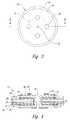
- FIG. 1is a plan view of the flexible connector according to one embodiment of the invention.
- FIG. 2is an enlarged view of a section of the flexible connector, showing the configuration of the contact pads, together with electrical traces.
- FIG. 3is a plan view of a single contact pad on the flexible connector.
- FIG. 4is a cross section of a single contact pad, together with the underlying structure, along the line 4 of FIG. 3 .
- FIG. 5shows a contact pad on a circuit board in electrical connection with the contact pad of the present invention.
- FIG. 1shows an electrical connector 8 .
- the electrical connector 8includes a flexible circuit material 10 having contact pads 12 thereon.
- this flexible substrate, or “flex”is a composite of materials commercially available, i.e., Dupont Pyralux Series.
- Contact pads 12are provided on the surface of the flexible substrate and configured such that they correspond to a configuration of contact pads on the surface of a circuit board or other device to which the connection is to be made. When these two surfaces are correctly aligned and brought into contact, each pad on the electrical connector 8 makes direct contact with a corresponding pad on the circuit board.
- this alignmentis achieved through the use of alignment holes 34 in the connector. These holes 34 are precisely positioned in relation to the contact pads 12 , and correspond to alignment features on the circuit board. A variety of fasteners and methods of alignment between the electrical connection and circuit board may be designed for use with this invention, and variations in such fall within the scope of this invention.
- the shape and size of the electrical connector 8is determined by the specific application.
- the version shown in FIG. 1represents one embodiment of this invention. Other applications will require other connector sizes and shapes, also within the scope of this invention.
- a plurality of flexible connectorsare formed on a master sheet, then individually cut to the appropriate size and shape.
- the fastenersmay be manufactured individually or concurrently with other devices. These are considered to be encompassed by the principles of the invention.
- FIG. 2shows an enlarged view of a portion of the surface of the connector 8 , on which the contact pads 12 are formed.
- the distance D between the padsis 0.05 inches, which achieves a density of 400 contacts per inch.
- Other configurations and densitiesare possible and may be preferable for specific applications.
- FIG. 3shows a plan view of a single contact pad 12 .
- the contact padsare round and have a diameter of 0.031 inches.
- Tiny bumps, also called micro-pads, 20are provided on the surface of the contact pad 12 , and comprise a part thereof.
- the size or shape of the contact padsmay vary, and the size shape or configuration of the micro-pads may vary. Such variations fall within the scope of this invention.
- FIG. 4shows a cross section view, at line 4 of FIG. 3, of a single contact pad 12 , together with the flexible circuit material 10 upon which it is formed.
- a commercially available flexible circuit materialis used.
- a first non-conductive substrate layer 28is processed, using known methods, to form highly conductive pads 14 on its first surface.
- non-conductive substratescan be purchased having highly conductive layers affixed to both sides thereof. These substrates can be purchased in various thicknesses, such as 0.001 inches, 0.002 inches, or any acceptable thickness.
- a commercial substrateis obtained having a conductive layer on both sides thereof. The conductive layer is then patterned and etched on each side, so as to form electrical traces at the desired locations. For example, one side thereof may become the ground plane and the other side thereof may be etched to form pad 14 , and electrical traces connected thereto.
- the pads 14may be copper and may have a thickness of 700 ⁇ inches.
- a second nonconductive substrate layer 32is processed, using known methods, to form electrical traces 36 on its second surface.
- the tracesmay be copper and may have a thickness of 700 ⁇ inches.
- a non-conductive bonding layer 30the first substrate layer 28 and the second substrate layer 32 are bonded together forming a composite flexible substrate, comprising the flexible circuit material 10 .
- an electrically conducted ground planemay be present between first substrate layer 28 and second substrate layer 32 . Connection to such a ground plane may be made by the same techniques by which connection is made to the electrical trace 36 as described later herein. Their positioning is such that the appropriate electrical traces 36 are directly opposite the corresponding pads 14 .
- additional electrical traceson other surfaces or layers of the flexible circuit material. This may include the formation of electrical traces concurrently, and on the same surface as the conductive pads. In other embodiments of the invention additional substrate layers may be used to accommodate the trace pattern and density desired.
- the thickness of the individual substrate layersmay be 0.001 inches, 0.002 inches, or any thickness or combination of thicknesses deemed appropriate.
- holes 22are drilled through the entire assembly, centered in each pad 14 .
- the holesmay have a diameter of 0.0065 inches.
- a highly conductive layer 24is plated on the pads 14 , the insides of the holes 22 , and that part of the traces 36 that lies directly opposite the pads, providing an electrically conductive path from the pad 14 to the trace 36 .
- This conductive layermay be copper or other conductor.
- a non-conductive cover layer 26is applied to both surfaces of the substrate 10 . The thickness of this layer is sufficient to provide insulation and protection from abrasion during normal handling and operation. This covers the traces 36 and the pads 14 as desired. According to one embodiment, this layer may have a thickness of 0.002 inches.
- An openingis provided in the layer 26 over the pad 14 , centered over the hole 22 . The opening may be produced by any appropriate techniques such as masking during formation, etching, milling, photo processing steps or the like.
- the cover layer 26forms a mask through which a conductive layer 16 is plated, primarily onto the surface of the preceding conductive plating 24 .
- this layeris copper or copper alloy, and is coplanar with the surface of the cover layer 26 .
- micro-pads 20are formed on the conductive layer 16 .
- the thickness of the micro-padsmay be 0.001 inches.
- a finish layer 18is formed on the surface of the plate layer 16 and the micro-pads 20 .
- the finish layer 18comprises three successive layers: 150 ⁇ inches of nickel, 15 ⁇ inches of palladium, and 3-7 ⁇ inches of gold in one embodiment.
- one acceptable technique for forming micro-pads 20is to provide a mask over each contact pad 12 and then, using appropriate electroplating techniques, plate the micro-pads 20 onto the conductive layer by electrical connection via the respective trace connected to the individual contact pads.
- An alternative techniqueis to form a layer thereover and then, using appropriate mask and etching techniques, remove the layer so as to provide the micro-bumps in the final shape as shown.
- the diameter of the micro-padsis selected to provide good electrical contact under the appropriate pressure when the contact pad is acting as an electrode for connection to a printed circuit board. As a general rule, it will have a surface area considerably smaller than the surface area of the large contact pad.
- the surface area of the micro-padsmay be in the range of 1% to 5% of the surface area of the contact pad 12 thus providing correspondingly increasing pressure at their contact points than would be provided across the wide surface area of contact layer 12 . They may also be provided in other shapes, such as pointed at the tapered square, cone shaped, pyramid shape, or other acceptable shapes for providing solid electrical contact.
- FIG. 5shows the individual contact pad 12 of FIG. 4, together with a contact pad 38 formed on a circuit board 40 .
- contact padsare provided on the surface of the circuit board, in a size and configuration corresponding to those on the connector. These pads may be formed using the same processes as, and concurrently with, the formation of other features of the circuit board.
- the contact pads 38 on the circuit boardare produced according to known principles.
- a holeis drilled and plated to form the contact pad.
- a feature known in the industry as a knee 41is formed on the edge of the hole during the plating process. This feature appears in FIG. 5 as a rise in the plate.
- the kneecan interfere with a solid electrical connection by preventing the contact pads from making full contact.
- the use of micro-padssolves this problem by straddling the knee and allowing good contact between the respective contact pads.
- the connectoris aligned with the circuit board such that the contact pads 12 of the connector are in contact with the appropriate contact pads 38 of the circuit board 40 , and sufficient pressure applied to ensure a solid connection.
- the micro-pads 20may, in some instances, bite slightly into the contact pad 38 to provide a high quality, low resistance electrical connection.
- the traces 36 of the connectorform conductive paths to electrically connect the circuit board to other electronic devices. These may include other circuit boards, modules, printers, computers etc.
- the connection with these other devicesmay be made by any means appropriate for the application, including conventional connectors, or some embodiment of this invention. may be made by any means appropriate for the application, including conventional connectors, or some embodiment of this invention.
- the surface 47 of the connector directly opposite the primary face of contact pad 12forms a contact pad which, when the connector is in place on the circuit board 40 , is in electrical continuity with the contact pad 38 .
- Another connector, stacked on surface 47would make contact, through the first connector, with the circuit board 40 . This feature allows the designer the liberty of using multiple connectors at the same site, permitting greater trace density or connection to multiple devices.
- the current carrying requirement of the connectorsis low as compared to that needed to power a computer.
- An important factor to consideris the security and dependability of the contacts. If the pressure between a flat contact pad of the connector and those of the circuit board is inadequate, the result may be either intermittent opening of the contact, which would interfere with the transmission of data, or increased resistance at the point of connection, raising the total impedance of the circuit to an unacceptable level.
- the design of fasteners and hardware used to exert force adequate to press the contacts of the connector onto those of the circuit boardis an important consideration.
- the use of micro-pads 20 on the surface of the contacts on the connectorcan significantly reduce the pressure requirements on the board as a whole while providing higher pressure at the actual points of contact, thus making possible the use of lighter, smaller fasteners in high density applications.
- the total surface area of the contactswould be 0.28 square inches per square inch of connector. This would require 14 pounds of pressure per square inch of connector.
- the micro-pads 20on the surface of the connectors, the surface area is reduced significantly.
- One embodiment of the inventionemploys four micro-pads per contact, with a diameter of 0.003 inches each. In other applications, the micro-pads may be 0.001 to 0.01 inches in diameter. If one assumes the same density of contacts, the total surface area is 0.011 square inches per square inch of connector.
- circuit boardin the foregoing description is for convenience only, and includes a broad range of electrical products.
- the connector and method described hereinmay be used to connect to any electronic device including circuit boards, modules, other connectors, peripheral devices etc.
Landscapes
- Engineering & Computer Science (AREA)
- Microelectronics & Electronic Packaging (AREA)
- Metallurgy (AREA)
- Manufacturing & Machinery (AREA)
- Printing Elements For Providing Electric Connections Between Printed Circuits (AREA)
- Coupling Device And Connection With Printed Circuit (AREA)
Abstract
Description
Claims (28)
Priority Applications (2)
| Application Number | Priority Date | Filing Date | Title |
|---|---|---|---|
| US09/705,368US6641406B1 (en) | 2000-11-03 | 2000-11-03 | Flexible connector for high density circuit applications |
| EP01410148AEP1204302A1 (en) | 2000-11-03 | 2001-11-05 | Flexible connector for high density circuit applications |
Applications Claiming Priority (1)
| Application Number | Priority Date | Filing Date | Title |
|---|---|---|---|
| US09/705,368US6641406B1 (en) | 2000-11-03 | 2000-11-03 | Flexible connector for high density circuit applications |
Publications (1)
| Publication Number | Publication Date |
|---|---|
| US6641406B1true US6641406B1 (en) | 2003-11-04 |
Family
ID=24833157
Family Applications (1)
| Application Number | Title | Priority Date | Filing Date |
|---|---|---|---|
| US09/705,368Expired - LifetimeUS6641406B1 (en) | 2000-11-03 | 2000-11-03 | Flexible connector for high density circuit applications |
Country Status (2)
| Country | Link |
|---|---|
| US (1) | US6641406B1 (en) |
| EP (1) | EP1204302A1 (en) |
Cited By (10)
| Publication number | Priority date | Publication date | Assignee | Title |
|---|---|---|---|---|
| US20050221635A1 (en)* | 2004-03-30 | 2005-10-06 | International Business Machines Corporation | Micro-bumps to enhance lga interconnections |
| US20150008577A1 (en)* | 2007-12-18 | 2015-01-08 | Micron Technology, Inc. | Methods of fluxless micro-piercing of solder balls, and resulting devices |
| US20150192633A1 (en)* | 2014-01-07 | 2015-07-09 | International Business Machines Corporation | 3d chip testing through micro-c4 interface |
| US20150264811A1 (en)* | 2014-03-14 | 2015-09-17 | Minebea Co., Ltd. | Flexible printed circuit board |
| EP3185371A1 (en) | 2015-12-22 | 2017-06-28 | Biosense Webster (Israel), Ltd. | Connectors having three-dimensional surfaces |
| EP3185366A1 (en) | 2015-12-22 | 2017-06-28 | Biosense Webster (Israel), Ltd. | Apparatus and method for preventing unwanted contact between terminals |
| US20180122847A1 (en)* | 2004-07-30 | 2018-05-03 | Sony Corporation | Semiconductor module, mos type solid-state image pickup device, camera and manufacturing method of camera |
| JP2021044374A (en)* | 2019-09-11 | 2021-03-18 | 大日本印刷株式会社 | Manufacturing method of through silicon via board, wiring board and wiring board |
| CN113438810A (en)* | 2021-05-18 | 2021-09-24 | 深圳市致趣科技有限公司 | Connector manufacturing method, electronic equipment, connector and application |
| CN115754138A (en)* | 2022-11-01 | 2023-03-07 | 中国原子能科学研究院 | Micro-grid structure gas detector |
Families Citing this family (1)
| Publication number | Priority date | Publication date | Assignee | Title |
|---|---|---|---|---|
| US8251494B2 (en) | 2009-11-30 | 2012-08-28 | Eastman Kodak Company | Bondable printed wiring with improved wear resistance |
Citations (11)
| Publication number | Priority date | Publication date | Assignee | Title |
|---|---|---|---|---|
| US4116517A (en) | 1976-04-15 | 1978-09-26 | International Telephone And Telegraph Corporation | Flexible printed circuit and electrical connection therefor |
| US4125310A (en) | 1975-12-01 | 1978-11-14 | Hughes Aircraft Co | Electrical connector assembly utilizing wafers for connecting electrical cables |
| US4420203A (en) | 1981-06-04 | 1983-12-13 | International Business Machines Corporation | Semiconductor module circuit interconnection system |
| EP0106990A1 (en) | 1982-09-23 | 1984-05-02 | Schoeller & Co. Elektronik GmbH | Contacting element for printed circuit boards |
| WO1988005217A1 (en) | 1986-12-29 | 1988-07-14 | Hughes Aircraft Company | Pressure connector for flexible cables and the like |
| FR2643754A1 (en) | 1989-02-28 | 1990-08-31 | Thomson Brandt Armements | PROCESS FOR MAKING A FLAT CONNECTION |
| US5307561A (en) | 1991-08-26 | 1994-05-03 | Hughes Aircraft Company | Method for making 3-D electrical circuitry |
| US5364277A (en) | 1990-09-11 | 1994-11-15 | Hughes Aircraft Company | Three-dimensional electroformed circuitry |
| US5929521A (en)* | 1997-03-26 | 1999-07-27 | Micron Technology, Inc. | Projected contact structure for bumped semiconductor device and resulting articles and assemblies |
| US6118080A (en)* | 1998-01-13 | 2000-09-12 | Micron Technology, Inc. | Z-axis electrical contact for microelectronic devices |
| US6230402B1 (en)* | 1999-02-17 | 2001-05-15 | Scitex Digital Printing, Inc. | Electrical contact termination for a flexible circuit |
- 2000
- 2000-11-03USUS09/705,368patent/US6641406B1/ennot_activeExpired - Lifetime
- 2001
- 2001-11-05EPEP01410148Apatent/EP1204302A1/ennot_activeWithdrawn
Patent Citations (12)
| Publication number | Priority date | Publication date | Assignee | Title |
|---|---|---|---|---|
| US4125310A (en) | 1975-12-01 | 1978-11-14 | Hughes Aircraft Co | Electrical connector assembly utilizing wafers for connecting electrical cables |
| US4116517A (en) | 1976-04-15 | 1978-09-26 | International Telephone And Telegraph Corporation | Flexible printed circuit and electrical connection therefor |
| US4420203A (en) | 1981-06-04 | 1983-12-13 | International Business Machines Corporation | Semiconductor module circuit interconnection system |
| EP0106990A1 (en) | 1982-09-23 | 1984-05-02 | Schoeller & Co. Elektronik GmbH | Contacting element for printed circuit boards |
| WO1988005217A1 (en) | 1986-12-29 | 1988-07-14 | Hughes Aircraft Company | Pressure connector for flexible cables and the like |
| FR2643754A1 (en) | 1989-02-28 | 1990-08-31 | Thomson Brandt Armements | PROCESS FOR MAKING A FLAT CONNECTION |
| US5364277A (en) | 1990-09-11 | 1994-11-15 | Hughes Aircraft Company | Three-dimensional electroformed circuitry |
| US5307561A (en) | 1991-08-26 | 1994-05-03 | Hughes Aircraft Company | Method for making 3-D electrical circuitry |
| US5354205A (en) | 1991-08-26 | 1994-10-11 | Hughes Aircraft Company | Electrical connections with shaped contacts |
| US5929521A (en)* | 1997-03-26 | 1999-07-27 | Micron Technology, Inc. | Projected contact structure for bumped semiconductor device and resulting articles and assemblies |
| US6118080A (en)* | 1998-01-13 | 2000-09-12 | Micron Technology, Inc. | Z-axis electrical contact for microelectronic devices |
| US6230402B1 (en)* | 1999-02-17 | 2001-05-15 | Scitex Digital Printing, Inc. | Electrical contact termination for a flexible circuit |
Cited By (24)
| Publication number | Priority date | Publication date | Assignee | Title |
|---|---|---|---|---|
| US20050221635A1 (en)* | 2004-03-30 | 2005-10-06 | International Business Machines Corporation | Micro-bumps to enhance lga interconnections |
| US20060030170A1 (en)* | 2004-03-30 | 2006-02-09 | Brody Jeffrey A | Micro-bumps to enhance LGA interconnections |
| US7302757B2 (en)* | 2004-03-30 | 2007-12-04 | International Business Machines Corporation | Micro-bumps to enhance LGA interconnections |
| US10586822B2 (en)* | 2004-07-30 | 2020-03-10 | Sony Corporation | Semiconductor module, MOS type solid-state image pickup device, camera and manufacturing method of camera |
| US20180122847A1 (en)* | 2004-07-30 | 2018-05-03 | Sony Corporation | Semiconductor module, mos type solid-state image pickup device, camera and manufacturing method of camera |
| US20150008577A1 (en)* | 2007-12-18 | 2015-01-08 | Micron Technology, Inc. | Methods of fluxless micro-piercing of solder balls, and resulting devices |
| US10515918B2 (en) | 2007-12-18 | 2019-12-24 | Micron Technology, Inc. | Methods of fluxless micro-piercing of solder balls, and resulting devices |
| US10163840B2 (en)* | 2007-12-18 | 2018-12-25 | Micron Technology, Inc. | Methods of fluxless micro-piercing of solder balls, and resulting devices |
| US20150192633A1 (en)* | 2014-01-07 | 2015-07-09 | International Business Machines Corporation | 3d chip testing through micro-c4 interface |
| US11193953B2 (en) | 2014-01-07 | 2021-12-07 | International Business Machines Corporation | 3D chip testing through micro-C4 interface |
| US9726691B2 (en)* | 2014-01-07 | 2017-08-08 | International Business Machines Corporation | 3D chip testing through micro-C4 interface |
| US10371717B2 (en) | 2014-01-07 | 2019-08-06 | International Business Machines Corporation | 3D chip testing through micro-C4 interface |
| US20150264811A1 (en)* | 2014-03-14 | 2015-09-17 | Minebea Co., Ltd. | Flexible printed circuit board |
| EP3185371A1 (en) | 2015-12-22 | 2017-06-28 | Biosense Webster (Israel), Ltd. | Connectors having three-dimensional surfaces |
| US10211559B2 (en)* | 2015-12-22 | 2019-02-19 | Biosense Webster (Israel) Ltd. | Preventing unwanted contact between terminals |
| US10128594B2 (en) | 2015-12-22 | 2018-11-13 | Biosense Webster (Israel) Ltd. | Connectors having three-dimensional surfaces |
| US10581191B2 (en) | 2015-12-22 | 2020-03-03 | Biosense Webster (Israel) Ltd. | Preventing unwanted contact between terminals |
| US9905956B2 (en) | 2015-12-22 | 2018-02-27 | Biosense Webster (Israel) Ltd. | Preventing unwanted contact between terminals |
| US10714861B1 (en)* | 2015-12-22 | 2020-07-14 | Biosense Webster (Israel) Ltd. | Preventing unwanted contact between terminals |
| EP3680994A1 (en) | 2015-12-22 | 2020-07-15 | Biosense Webster (Israel) Ltd. | Connectors having three-dimensional surfaces |
| EP3185366A1 (en) | 2015-12-22 | 2017-06-28 | Biosense Webster (Israel), Ltd. | Apparatus and method for preventing unwanted contact between terminals |
| JP2021044374A (en)* | 2019-09-11 | 2021-03-18 | 大日本印刷株式会社 | Manufacturing method of through silicon via board, wiring board and wiring board |
| CN113438810A (en)* | 2021-05-18 | 2021-09-24 | 深圳市致趣科技有限公司 | Connector manufacturing method, electronic equipment, connector and application |
| CN115754138A (en)* | 2022-11-01 | 2023-03-07 | 中国原子能科学研究院 | Micro-grid structure gas detector |
Also Published As
| Publication number | Publication date |
|---|---|
| EP1204302A1 (en) | 2002-05-08 |
Similar Documents
| Publication | Publication Date | Title |
|---|---|---|
| US6524115B1 (en) | Compliant interconnect assembly | |
| US5451169A (en) | Connector with monolithic multi-contact array | |
| JP3741574B2 (en) | Flexible circuit compression connector system and manufacturing method thereof | |
| US4125310A (en) | Electrical connector assembly utilizing wafers for connecting electrical cables | |
| JP2620502B2 (en) | Electrical interconnects and assemblies with helical contacts | |
| US7587817B2 (en) | Method of making electrical connector on a flexible carrier | |
| US5199879A (en) | Electrical assembly with flexible circuit | |
| US5526565A (en) | High density self-aligning conductive networks and contact clusters and method and apparatus for making same | |
| US7383632B2 (en) | Method for fabricating a connector | |
| US5334029A (en) | High density connector for stacked circuit boards | |
| US4435740A (en) | Electric circuit packaging member | |
| US5173055A (en) | Area array connector | |
| US20020098721A1 (en) | Shielded carrier for land grid array connectors and a process for fabricating same | |
| EP0343021A1 (en) | Flex dot wafer probe | |
| JP3180193B2 (en) | Compression connector | |
| JPH07263830A (en) | Cavity and ridge interconnect structure for electronic packages | |
| US6641406B1 (en) | Flexible connector for high density circuit applications | |
| JPH0329284A (en) | Connector and forming method of the same | |
| US6638077B1 (en) | Shielded carrier with components for land grid array connectors | |
| US4187388A (en) | Circuit board with self-locking terminals | |
| US6540527B1 (en) | Method and adapter for reworking a circuit containing an LGA device | |
| JPH0778645A (en) | Connector for electrical connection | |
| JP2549125Y2 (en) | Connector for electrical connection | |
| JPH0639484Y2 (en) | Printed circuit board connection structure | |
| EP0532926B1 (en) | Electrical circuit with resilient gasket support for raised connection features |
Legal Events
| Date | Code | Title | Description |
|---|---|---|---|
| AS | Assignment | Owner name:CRAY INC., WASHINGTON Free format text:ASSIGNMENT OF ASSIGNORS INTEREST;ASSIGNORS:YATSKOV, ALEXANDER I.;HELLRIEGEL, STEPHEN V.R.;REEL/FRAME:011657/0054;SIGNING DATES FROM 20010130 TO 20010131 | |
| AS | Assignment | Owner name:FOOTHILL CAPITAL CORPORATION (A CALIFORNIA CORPORA Free format text:SECURITY INTEREST;ASSIGNOR:CRAY, INC. (A WASHINGTON CORPORATION);REEL/FRAME:011763/0716 Effective date:20010328 | |
| STCF | Information on status: patent grant | Free format text:PATENTED CASE | |
| AS | Assignment | Owner name:WELLS FARGO BANK, N.A.,CALIFORNIA Free format text:SECURITY AGREEMENT;ASSIGNOR:CRAY INC.;REEL/FRAME:016446/0675 Effective date:20050531 Owner name:WELLS FARGO BANK, N.A., CALIFORNIA Free format text:SECURITY AGREEMENT;ASSIGNOR:CRAY INC.;REEL/FRAME:016446/0675 Effective date:20050531 | |
| FPAY | Fee payment | Year of fee payment:4 | |
| FPAY | Fee payment | Year of fee payment:8 | |
| FEPP | Fee payment procedure | Free format text:PAYOR NUMBER ASSIGNED (ORIGINAL EVENT CODE: ASPN); ENTITY STATUS OF PATENT OWNER: LARGE ENTITY | |
| FPAY | Fee payment | Year of fee payment:12 | |
| AS | Assignment | Owner name:CRAY INC., WASHINGTON Free format text:RELEASE BY SECURED PARTY;ASSIGNOR:WELLS FARGO CAPITAL FINANCE, LLC, SUCCESSOR BY MERGER OF WELLS FARGO CAPITAL FINANCE, INC., FORMERLY KNOWN AS WELLS FARGO FOOTHILL, INC., FORMERLY KNOWN AS FOOTHILL CAPITAL CORPORATION;REEL/FRAME:049837/0709 Effective date:20190626 Owner name:CRAY INC., WASHINGTON Free format text:RELEASE BY SECURED PARTY;ASSIGNOR:WELLS FARGO BANK N.A.;REEL/FRAME:049837/0847 Effective date:20190626 |