US6641273B1 - MEMS structure with mechanical overdeflection limiter - Google Patents
MEMS structure with mechanical overdeflection limiterDownload PDFInfo
- Publication number
- US6641273B1 US6641273B1US10/186,566US18656602AUS6641273B1US 6641273 B1US6641273 B1US 6641273B1US 18656602 AUS18656602 AUS 18656602AUS 6641273 B1US6641273 B1US 6641273B1
- Authority
- US
- United States
- Prior art keywords
- mirror
- gimbal
- overhanging structure
- hinge structures
- pair
- Prior art date
- Legal status (The legal status is an assumption and is not a legal conclusion. Google has not performed a legal analysis and makes no representation as to the accuracy of the status listed.)
- Expired - Lifetime
Links
Images


Classifications
- B—PERFORMING OPERATIONS; TRANSPORTING
- B81—MICROSTRUCTURAL TECHNOLOGY
- B81B—MICROSTRUCTURAL DEVICES OR SYSTEMS, e.g. MICROMECHANICAL DEVICES
- B81B3/00—Devices comprising flexible or deformable elements, e.g. comprising elastic tongues or membranes
- B81B3/0035—Constitution or structural means for controlling the movement of the flexible or deformable elements
- B81B3/0051—For defining the movement, i.e. structures that guide or limit the movement of an element
- G—PHYSICS
- G02—OPTICS
- G02B—OPTICAL ELEMENTS, SYSTEMS OR APPARATUS
- G02B26/00—Optical devices or arrangements for the control of light using movable or deformable optical elements
- G02B26/08—Optical devices or arrangements for the control of light using movable or deformable optical elements for controlling the direction of light
- G02B26/0816—Optical devices or arrangements for the control of light using movable or deformable optical elements for controlling the direction of light by means of one or more reflecting elements
- G02B26/0833—Optical devices or arrangements for the control of light using movable or deformable optical elements for controlling the direction of light by means of one or more reflecting elements the reflecting element being a micromechanical device, e.g. a MEMS mirror, DMD
- G02B26/0841—Optical devices or arrangements for the control of light using movable or deformable optical elements for controlling the direction of light by means of one or more reflecting elements the reflecting element being a micromechanical device, e.g. a MEMS mirror, DMD the reflecting element being moved or deformed by electrostatic means
- B—PERFORMING OPERATIONS; TRANSPORTING
- B81—MICROSTRUCTURAL TECHNOLOGY
- B81B—MICROSTRUCTURAL DEVICES OR SYSTEMS, e.g. MICROMECHANICAL DEVICES
- B81B2201/00—Specific applications of microelectromechanical systems
- B81B2201/04—Optical MEMS
- B81B2201/042—Micromirrors, not used as optical switches
Definitions
- This inventionrelates to electromechanical components such as micro electrical mechanical system (MEMS) devices or MEMS arrays and particularly to electrostatically-actuated electro-mechanical components wherein undesired deflection of movable elements due to nonlinear attractive effect may be controlled, preventing device failure.
- Components constructed according to the inventionare MEMS mirror arrays or other micromachined elements.
- MEMS array structurescomprise Silicon on Insulator (SOI) array structures on which is fabricated an integrated electrode array.
- SOISilicon on Insulator
- a solutionis needed that limits the maximum deflection of the MEMS device due to inherent electrostatic parallel plate instability without compromising device performance or manufacturability.
- a MEMS devicehaving a fixed element and a movable element wherein one of the fixed element and the movable element has at least one radially-extended stop or overdeflection limiter.
- a fixed overlayer plateforms an aperture. The aperture is sized to minimize vignetting and may be beveled on the margin. Overdeflection limitation occurs during deflection before the movable element can impinge on an underlying electrode.
- the overdeflection limitermay be conveniently placed adjacent a gimbaled hinge.
- the mechanical stopmay be a plate mounted to the top of a conventional MEMS structure or integrated into a three layer MEMS structure or two two-layer MEMS structures combined.
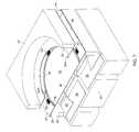
- FIG. 1is a perspective view in cutaway of a first embodiment according to the invention of a double-gimbaled mirror with a top mounted overhang stop layer.
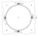
- FIG. 2is a top view of a double gimbaled mirror with mechanical stop tabs extending from the mirror.
- FIG. 3is a side cross-sectional view of a single array element with a flipped SOI overhang mounted on a standoff.
- FIG. 4is a side cross-sectional view of a single array element with an overhang formed in a single process step as a bevel.
- FIG. 5is a perspective view of the element of FIG. 4 .
- FIG. 6is a side cross-sectional view of a single array element with an overhang of multiple bonded wafers.
- FIG. 7is a perspective view in cutaway of a first embodiment according to the invention of a double-gimbaled mirror with a top mounted overhang stop layer.
- FIG. 1there is shown a perspective view in cutaway of a first embodiment of a single array element 10 of a MEMS array according to the invention.
- a mirror 12is mounted on a first pair of hinges (FIG. 2) 14 , 16 to a gimbal 18 .
- the gimbal 18is connected by a second pair of hinges 20 , 22 having one degree of freedom to a frame 24 , more particularly to a cantilever 26 of the frame 24 wherein an oxide layer 25 (FIG. 3) is provided for bonding and etch stop during manufacturing.
- the oxide layer 24is typically on the order of only one micron thick.
- the nature of the frame constructionis immaterial so long as it provides support.
- an overhang 28is provided which serves as a mechanical stop against rotation of the mirror 12 .
- the overhang 28is typically mounted above the mirror 12 (i.e., outside the electrode cavity) as part of a cap 30 .
- tab extensions 32 , 34extend from the mirror 12 adjacent the second hinge pair 20 , 22 .
- an alternative and less desirable embodimentemploys tab extensions 32 A, 34 A which extend from the overhang 28 to encounter the edge of the mirror 12 . While the tab extension allow for reduced mirror mass, they potentially vignette the beam to result in signal loss.
- the frame 24spaces the mirror from electrodes 36 - 39 mounted on a substrate 40 .
- a dielectric 42spaces the frame 24 from the substrate 40 , and a plurality of standoffs 44 , of which only one is shown in FIGS. 1 or 7 ) separate the cap 30 from the frame.
- the standoffs 44can be either insulative or conductive. Insulative standoffs are useful if there is a circuit to be formed that senses contact between the mirror and the overhang indicating overdeflection. Conductive standoffs make it easier to construct a conductive cap 30 , thus maintaining the mirror 12 and the cap 30 at equal potential.
- FIG. 3illustrates in cross section a view of FIG. 1 or 2 along sight line 3 — 3 through tabs 32 , 34 , gimbal 18 and cantilever 26 .
- the overhang 28is an aperture plate mounted on standoffs 44 , which in this embodiment is a separately-formed layer formed on the cap 30 .
- the cap 30 and overhang 28are typically SOI structures (Silicon on Insulator where two different silicon layers are typically bonded together but separated by an oxide) which are “flipped” after fabrication and mounted by an appropriate adhesive such as an epoxy to standoffs 44 , which could be cylinders, beads or the like.
- the top layer of the mirror 12 on its frame 24could be etched to match a complementary cross etch in the mating face of the overhang 28 to assure accurate seating when beads are used as spacers.
- a KOH etch techniquecould be used wherein the crystal structures of the respective SOI chips are cross-ways to one another.
- FIG. 4is a side cross-sectional view of a single array element along sight line 4 — 4 with a typical deep KOH etch along exposed crystal planes to form an aperture 30 A .
- the aperture 30 A(FIG. 5) is a rectangle with exposed facets 52 - 56 , etc. It can be attached in the same manner as the structure of FIG. 3 with an appropriate adhesive to standoffs 44 .
- FIG. 6is a side cross-sectional view of a single array element with multiple bonds of SOI, so-called triple-stacked SOI.
- a dielectric 42separates electrodes 38 , 39 from the frame 40 , and an oxide layer 25 is disposed between the frame 40 and the layer forming the mirror 12 .
- a further oxide layer 27is disposed between the layer of the mirror 12 and a further silicon cap 30 , which in this case is step etched (before bonding) to form a shelf 31 .
- the cap 30is bonded to the layer of the mirror 12 at the oxide layer 27 after the oxidation and release step of the manufacturing process.
Landscapes
- Physics & Mathematics (AREA)
- General Physics & Mathematics (AREA)
- Optics & Photonics (AREA)
- Engineering & Computer Science (AREA)
- Computer Hardware Design (AREA)
- Microelectronics & Electronic Packaging (AREA)
- Micromachines (AREA)
Abstract
Description
Claims (11)
Priority Applications (4)
| Application Number | Priority Date | Filing Date | Title |
|---|---|---|---|
| US10/186,566US6641273B1 (en) | 2002-06-28 | 2002-06-28 | MEMS structure with mechanical overdeflection limiter |
| AU2003256311AAU2003256311A1 (en) | 2002-06-28 | 2003-06-24 | Mems structure with mechanical overdeflection limiter |
| PCT/US2003/020143WO2004003619A1 (en) | 2002-06-28 | 2003-06-24 | Mems structure with mechanical overdeflection limiter |
| US10/625,883US6805454B2 (en) | 2002-06-28 | 2003-07-22 | MEMS structure with mechanical overdeflection limiter |
Applications Claiming Priority (1)
| Application Number | Priority Date | Filing Date | Title |
|---|---|---|---|
| US10/186,566US6641273B1 (en) | 2002-06-28 | 2002-06-28 | MEMS structure with mechanical overdeflection limiter |
Related Child Applications (1)
| Application Number | Title | Priority Date | Filing Date |
|---|---|---|---|
| US10/625,883DivisionUS6805454B2 (en) | 2002-06-28 | 2003-07-22 | MEMS structure with mechanical overdeflection limiter |
Publications (1)
| Publication Number | Publication Date |
|---|---|
| US6641273B1true US6641273B1 (en) | 2003-11-04 |
Family
ID=29270104
Family Applications (2)
| Application Number | Title | Priority Date | Filing Date |
|---|---|---|---|
| US10/186,566Expired - LifetimeUS6641273B1 (en) | 2002-06-28 | 2002-06-28 | MEMS structure with mechanical overdeflection limiter |
| US10/625,883Expired - LifetimeUS6805454B2 (en) | 2002-06-28 | 2003-07-22 | MEMS structure with mechanical overdeflection limiter |
Family Applications After (1)
| Application Number | Title | Priority Date | Filing Date |
|---|---|---|---|
| US10/625,883Expired - LifetimeUS6805454B2 (en) | 2002-06-28 | 2003-07-22 | MEMS structure with mechanical overdeflection limiter |
Country Status (3)
| Country | Link |
|---|---|
| US (2) | US6641273B1 (en) |
| AU (1) | AU2003256311A1 (en) |
| WO (1) | WO2004003619A1 (en) |
Cited By (9)
| Publication number | Priority date | Publication date | Assignee | Title |
|---|---|---|---|---|
| EP1950174A2 (en) | 2007-01-25 | 2008-07-30 | Samsung Electro-Mechanics Co., Ltd. | MEMS Device with movement limiting arrangement |
| US20100103492A1 (en)* | 2008-10-29 | 2010-04-29 | Kabushiki Kaisha Topcon | MEMS-scanning mirror device and method for manufacturing the same |
| GB2506171A (en)* | 2012-09-24 | 2014-03-26 | Wolfson Microelectronics Plc | Preventing excess membrane excursions in a MEMS transducer |
| US20140268268A1 (en)* | 2013-03-15 | 2014-09-18 | Rit Technologies Ltd. | Electrostatically steerable actuator |
| US20150253566A1 (en)* | 2014-03-05 | 2015-09-10 | Palo Alto Research Center Incorporated | Aperture for illuminating micromirror arrays having mirror tilt axis not parallel with an array axis |
| CN108602662A (en)* | 2016-01-12 | 2018-09-28 | 通快瑞士股份公司 | Equipment for two-dimensionally deflecting laser beam |
| US11212624B2 (en)* | 2018-09-06 | 2021-12-28 | Infineon Technologies Ag | MEMS-transducer and method for producing a MEMS-transducer |
| US20220137398A1 (en)* | 2020-10-30 | 2022-05-05 | Ricoh Company, Ltd. | Light deflector, analyzer, resin identification system, and distance measurement device |
| US12253391B2 (en) | 2018-05-24 | 2025-03-18 | The Research Foundation For The State University Of New York | Multielectrode capacitive sensor without pull-in risk |
Families Citing this family (3)
| Publication number | Priority date | Publication date | Assignee | Title |
|---|---|---|---|---|
| TWI256940B (en)* | 2004-06-18 | 2006-06-21 | Walsin Lihwa Corp | Integration manufacturing process for MEMS element |
| WO2006069305A2 (en)* | 2004-12-22 | 2006-06-29 | University Of Virginia Patent Foundation | The use of microwaves for thermal and non-thermal applications in micro and nanoscale devices |
| US9672289B1 (en) | 2013-07-23 | 2017-06-06 | Plentyoffish Media Ulc | Apparatus, method and article to facilitate matching of clients in a networked environment |
Citations (8)
| Publication number | Priority date | Publication date | Assignee | Title |
|---|---|---|---|---|
| US4337506A (en)* | 1978-12-20 | 1982-06-29 | Terada James I | Adjustable lamp |
| US4598585A (en)* | 1984-03-19 | 1986-07-08 | The Charles Stark Draper Laboratory, Inc. | Planar inertial sensor |
| US4721274A (en)* | 1985-08-21 | 1988-01-26 | Erb Robert C | Gimbal assembly |
| US5016072A (en)* | 1988-01-13 | 1991-05-14 | The Charles Stark Draper Laboratory, Inc. | Semiconductor chip gyroscopic transducer |
| US5488862A (en)* | 1993-10-18 | 1996-02-06 | Armand P. Neukermans | Monolithic silicon rate-gyro with integrated sensors |
| WO2001004680A1 (en) | 1999-07-13 | 2001-01-18 | Input Output, Inc. | Micro-machined mirror device |
| US6337760B1 (en)* | 2000-07-17 | 2002-01-08 | Reflectivity, Inc. | Encapsulated multi-directional light beam steering device |
| US6379510B1 (en)* | 2000-11-16 | 2002-04-30 | Jonathan S. Kane | Method of making a low voltage micro-mirror array light beam switch |
- 2002
- 2002-06-28USUS10/186,566patent/US6641273B1/ennot_activeExpired - Lifetime
- 2003
- 2003-06-24AUAU2003256311Apatent/AU2003256311A1/ennot_activeAbandoned
- 2003-06-24WOPCT/US2003/020143patent/WO2004003619A1/ennot_activeApplication Discontinuation
- 2003-07-22USUS10/625,883patent/US6805454B2/ennot_activeExpired - Lifetime
Patent Citations (11)
| Publication number | Priority date | Publication date | Assignee | Title |
|---|---|---|---|---|
| US4337506A (en)* | 1978-12-20 | 1982-06-29 | Terada James I | Adjustable lamp |
| US4598585A (en)* | 1984-03-19 | 1986-07-08 | The Charles Stark Draper Laboratory, Inc. | Planar inertial sensor |
| US4721274A (en)* | 1985-08-21 | 1988-01-26 | Erb Robert C | Gimbal assembly |
| US5016072A (en)* | 1988-01-13 | 1991-05-14 | The Charles Stark Draper Laboratory, Inc. | Semiconductor chip gyroscopic transducer |
| US5488862A (en)* | 1993-10-18 | 1996-02-06 | Armand P. Neukermans | Monolithic silicon rate-gyro with integrated sensors |
| US5648618A (en)* | 1993-10-18 | 1997-07-15 | Armand P. Neukermans | Micromachined hinge having an integral torsion sensor |
| WO2001004680A1 (en) | 1999-07-13 | 2001-01-18 | Input Output, Inc. | Micro-machined mirror device |
| US6315423B1 (en) | 1999-07-13 | 2001-11-13 | Input/Output, Inc. | Micro machined mirror |
| US20020012180A1 (en) | 1999-07-13 | 2002-01-31 | Duli Yu | Dual axis micro-machined mirror device |
| US6337760B1 (en)* | 2000-07-17 | 2002-01-08 | Reflectivity, Inc. | Encapsulated multi-directional light beam steering device |
| US6379510B1 (en)* | 2000-11-16 | 2002-04-30 | Jonathan S. Kane | Method of making a low voltage micro-mirror array light beam switch |
Cited By (20)
| Publication number | Priority date | Publication date | Assignee | Title |
|---|---|---|---|---|
| EP1950174A2 (en) | 2007-01-25 | 2008-07-30 | Samsung Electro-Mechanics Co., Ltd. | MEMS Device with movement limiting arrangement |
| US20080179988A1 (en)* | 2007-01-25 | 2008-07-31 | Samsung Electro-Mechanics Co., Ltd. | Mems device and fabrication method of the same |
| US7800280B2 (en)* | 2007-01-25 | 2010-09-21 | Samsung Electro-Mechanics Co., Ltd | MEMS device and fabrication method of the same |
| US20100304517A1 (en)* | 2007-01-25 | 2010-12-02 | Samsung Electro-Mechanics Co., Ltd. | Mems device and fabrication method of the same |
| EP1950174A3 (en)* | 2007-01-25 | 2011-06-08 | Samsung Electro-Mechanics Co., Ltd. | MEMS Device with movement limiting arrangement |
| US7977207B2 (en) | 2007-01-25 | 2011-07-12 | Samsung Electro Mechanics Co., Ltd | MEMS device and fabrication method of the same |
| US20100103492A1 (en)* | 2008-10-29 | 2010-04-29 | Kabushiki Kaisha Topcon | MEMS-scanning mirror device and method for manufacturing the same |
| US8279509B2 (en) | 2008-10-29 | 2012-10-02 | Kabushiki Kaisha Topcon | MEMS-scanning mirror device and method for manufacturing the same |
| GB2506171B (en)* | 2012-09-24 | 2015-01-28 | Wolfson Microelectronics Plc | MEMS device and process |
| GB2506171A (en)* | 2012-09-24 | 2014-03-26 | Wolfson Microelectronics Plc | Preventing excess membrane excursions in a MEMS transducer |
| US9584903B2 (en) | 2012-09-24 | 2017-02-28 | Cirrus Logic, Inc. | MEMS device and process |
| US20140268268A1 (en)* | 2013-03-15 | 2014-09-18 | Rit Technologies Ltd. | Electrostatically steerable actuator |
| US9335544B2 (en)* | 2013-03-15 | 2016-05-10 | Rit Wireless Ltd. | Electrostatically steerable actuator |
| US20150253566A1 (en)* | 2014-03-05 | 2015-09-10 | Palo Alto Research Center Incorporated | Aperture for illuminating micromirror arrays having mirror tilt axis not parallel with an array axis |
| US9519135B2 (en)* | 2014-03-05 | 2016-12-13 | Palo Alto Research Center Incorporated | Aperture for illuminating micromirror arrays having mirror tilt axis not parallel with an array axis |
| CN108602662A (en)* | 2016-01-12 | 2018-09-28 | 通快瑞士股份公司 | Equipment for two-dimensionally deflecting laser beam |
| CN108602662B (en)* | 2016-01-12 | 2023-05-30 | 通快瑞士股份公司 | Device for deflecting a laser beam in two dimensions |
| US12253391B2 (en) | 2018-05-24 | 2025-03-18 | The Research Foundation For The State University Of New York | Multielectrode capacitive sensor without pull-in risk |
| US11212624B2 (en)* | 2018-09-06 | 2021-12-28 | Infineon Technologies Ag | MEMS-transducer and method for producing a MEMS-transducer |
| US20220137398A1 (en)* | 2020-10-30 | 2022-05-05 | Ricoh Company, Ltd. | Light deflector, analyzer, resin identification system, and distance measurement device |
Also Published As
| Publication number | Publication date |
|---|---|
| AU2003256311A1 (en) | 2004-01-19 |
| US6805454B2 (en) | 2004-10-19 |
| WO2004003619A1 (en) | 2004-01-08 |
| US20040001263A1 (en) | 2004-01-01 |
Similar Documents
| Publication | Publication Date | Title |
|---|---|---|
| US7420318B1 (en) | Lateral piezoelectric microelectromechanical system (MEMS) actuation and sensing device | |
| JP6093788B2 (en) | Method of making a device, semiconductor device and precursor structure | |
| US7466474B2 (en) | Micromechanical device with tilted electrodes | |
| US6641273B1 (en) | MEMS structure with mechanical overdeflection limiter | |
| US7872394B1 (en) | MEMS device with two axes comb drive actuators | |
| US6829937B2 (en) | Monolithic silicon acceleration sensor | |
| US6621135B1 (en) | Microrelays and microrelay fabrication and operating methods | |
| US20090302716A1 (en) | Piezoelectric device | |
| US7986073B2 (en) | Micro-electro mechanical system using snapping tabs, comb and parallel plate actuation | |
| US10411182B2 (en) | Drive apparatus | |
| KR20090098801A (en) | Micromirror actuators with encapsulation potential and methods for their preparation | |
| JP5038732B2 (en) | Optical scanning mirror | |
| JP3050164B2 (en) | Microactuator and manufacturing method thereof | |
| EP1514122B1 (en) | Method of manufacturing of a monolithic silicon acceleration sensor | |
| US20060050421A1 (en) | Adaptive mirror system | |
| US7487678B2 (en) | Z offset MEMS devices and methods | |
| JP4858064B2 (en) | Mechanical quantity detection sensor and manufacturing method thereof | |
| US20080229827A1 (en) | Electronic part, method for fabricating electronic part, acceleration sensor, and method for fabricating acceleration sensor | |
| JP2010147285A (en) | Mems, vibration gyroscope, and method of manufacturing mems | |
| US20060050419A1 (en) | Integrated wavefront correction module | |
| JP2009075209A (en) | Mirror device, optical component using the same and optical switch | |
| JP3533514B2 (en) | Electrostatic actuator and manufacturing method thereof | |
| JP5014589B2 (en) | MEMS package | |
| US9397585B2 (en) | MEMS shock cushion spring systems and methods | |
| JPH11356065A (en) | Microactuator |
Legal Events
| Date | Code | Title | Description |
|---|---|---|---|
| AS | Assignment | Owner name:GLIMMERGLASS NETWORKS, INC., CALIFORNIA Free format text:ASSIGNMENT OF ASSIGNORS INTEREST;ASSIGNORS:STAKER, BRYAN P.;SPALLAS, JAMES P.;MURAY, LAWRENCE P.;AND OTHERS;REEL/FRAME:013072/0717 Effective date:20020625 | |
| STCF | Information on status: patent grant | Free format text:PATENTED CASE | |
| FPAY | Fee payment | Year of fee payment:4 | |
| FPAY | Fee payment | Year of fee payment:8 | |
| AS | Assignment | Owner name:SQUARE 1 BANK, NORTH CAROLINA Free format text:SECURITY AGREEMENT;ASSIGNOR:GLIMMERGLASS NETWORKS, INC.;REEL/FRAME:026217/0067 Effective date:20110419 | |
| AS | Assignment | Owner name:GLIMMERGLASS NETWORKS, INC., CALIFORNIA Free format text:RELEASE OF SECURITY INTEREST;ASSIGNOR:SQUARE 1 BANK;REEL/FRAME:033522/0086 Effective date:20140624 | |
| FPAY | Fee payment | Year of fee payment:12 | |
| AS | Assignment | Owner name:SILICON VALLEY BANK, CALIFORNIA Free format text:SECURITY INTEREST;ASSIGNOR:GLIMMERGLASS NETWORKS, INC.;REEL/FRAME:037551/0296 Effective date:20160115 | |
| AS | Assignment | Owner name:DICON FIBEROPTICS, INC., CALIFORNIA Free format text:ASSIGNMENT OF ASSIGNORS INTEREST;ASSIGNOR:MOLEX, LLC;REEL/FRAME:051952/0931 Effective date:20200210 |