US6639866B2 - Very small swing high performance asynchronous CMOS static memory (multi-port register file) with power reducing column multiplexing scheme - Google Patents
Very small swing high performance asynchronous CMOS static memory (multi-port register file) with power reducing column multiplexing schemeDownload PDFInfo
- Publication number
- US6639866B2 US6639866B2US10/012,858US1285801AUS6639866B2US 6639866 B2US6639866 B2US 6639866B2US 1285801 AUS1285801 AUS 1285801AUS 6639866 B2US6639866 B2US 6639866B2
- Authority
- US
- United States
- Prior art keywords
- memory
- register file
- coupled
- port
- file memory
- Prior art date
- Legal status (The legal status is an assumption and is not a legal conclusion. Google has not performed a legal analysis and makes no representation as to the accuracy of the status listed.)
- Expired - Lifetime, expires
Links
Images


Classifications
- G—PHYSICS
- G11—INFORMATION STORAGE
- G11C—STATIC STORES
- G11C7/00—Arrangements for writing information into, or reading information out from, a digital store
- G11C7/02—Arrangements for writing information into, or reading information out from, a digital store with means for avoiding parasitic signals
- G—PHYSICS
- G11—INFORMATION STORAGE
- G11C—STATIC STORES
- G11C11/00—Digital stores characterised by the use of particular electric or magnetic storage elements; Storage elements therefor
- G11C11/21—Digital stores characterised by the use of particular electric or magnetic storage elements; Storage elements therefor using electric elements
- G11C11/34—Digital stores characterised by the use of particular electric or magnetic storage elements; Storage elements therefor using electric elements using semiconductor devices
- G11C11/40—Digital stores characterised by the use of particular electric or magnetic storage elements; Storage elements therefor using electric elements using semiconductor devices using transistors
- G11C11/41—Digital stores characterised by the use of particular electric or magnetic storage elements; Storage elements therefor using electric elements using semiconductor devices using transistors forming static cells with positive feedback, i.e. cells not needing refreshing or charge regeneration, e.g. bistable multivibrator or Schmitt trigger
- G11C11/412—Digital stores characterised by the use of particular electric or magnetic storage elements; Storage elements therefor using electric elements using semiconductor devices using transistors forming static cells with positive feedback, i.e. cells not needing refreshing or charge regeneration, e.g. bistable multivibrator or Schmitt trigger using field-effect transistors only
- G—PHYSICS
- G11—INFORMATION STORAGE
- G11C—STATIC STORES
- G11C11/00—Digital stores characterised by the use of particular electric or magnetic storage elements; Storage elements therefor
- G11C11/21—Digital stores characterised by the use of particular electric or magnetic storage elements; Storage elements therefor using electric elements
- G11C11/34—Digital stores characterised by the use of particular electric or magnetic storage elements; Storage elements therefor using electric elements using semiconductor devices
- G11C11/40—Digital stores characterised by the use of particular electric or magnetic storage elements; Storage elements therefor using electric elements using semiconductor devices using transistors
- G11C11/41—Digital stores characterised by the use of particular electric or magnetic storage elements; Storage elements therefor using electric elements using semiconductor devices using transistors forming static cells with positive feedback, i.e. cells not needing refreshing or charge regeneration, e.g. bistable multivibrator or Schmitt trigger
- G11C11/413—Auxiliary circuits, e.g. for addressing, decoding, driving, writing, sensing, timing or power reduction
- G11C11/417—Auxiliary circuits, e.g. for addressing, decoding, driving, writing, sensing, timing or power reduction for memory cells of the field-effect type
- G11C11/419—Read-write [R-W] circuits
- G—PHYSICS
- G11—INFORMATION STORAGE
- G11C—STATIC STORES
- G11C7/00—Arrangements for writing information into, or reading information out from, a digital store
- G11C7/06—Sense amplifiers; Associated circuits, e.g. timing or triggering circuits
- G11C7/062—Differential amplifiers of non-latching type, e.g. comparators, long-tailed pairs
- G—PHYSICS
- G11—INFORMATION STORAGE
- G11C—STATIC STORES
- G11C7/00—Arrangements for writing information into, or reading information out from, a digital store
- G11C7/06—Sense amplifiers; Associated circuits, e.g. timing or triggering circuits
- G11C7/067—Single-ended amplifiers
- G—PHYSICS
- G11—INFORMATION STORAGE
- G11C—STATIC STORES
- G11C8/00—Arrangements for selecting an address in a digital store
- G11C8/16—Multiple access memory array, e.g. addressing one storage element via at least two independent addressing line groups
- G—PHYSICS
- G11—INFORMATION STORAGE
- G11C—STATIC STORES
- G11C2207/00—Indexing scheme relating to arrangements for writing information into, or reading information out from, a digital store
- G11C2207/06—Sense amplifier related aspects
- G11C2207/063—Current sense amplifiers
Definitions
- One embodiment of the present inventionrelates to static memories or multi-port register files. More specifically, one embodiment of the present invention relates to very small swing high performance asynchronous CMOS static memory having a column multiplexing scheme.
- memories or register filesare widely used in numerous applications in various industries. Although, typically it is desirable to incorporate as many memory cells as possible into a given area, some known memories or register files are often perceived as physically too large (i.e., they take up too much silicon area) and/or are too slow for a given product definition. In addition, power dissipation is another parameter that all memory designers are forced to consider in order to make a product cost effective. Additionally, some applications demand that such memories or register files function synchronously or asynchronously.
- CMOS static random access memory(alternatively referred to as the “SRAM”), which retains its memory state without refreshing as long as power is supplied to the cell.
- the memory stateis usually stored as a voltage differential within a bistable functional element such as an inverter loop.
- SRAM memoriesdon't work in conjunction with low supply voltages. That is, as the supply voltage approaches about 1.0 volt or less, the access time increases exponentially.
- SRAM memoriesare susceptible to noise. That is noise may be present, on a bitline for example, and may false trip one or more associated devices such as sense amplifiers.
- CMOS static memorymay be found in a high performance CMOS static memory.
- the present inventionmay be found in a differential high speed CMOS static memory that operates synchronously or asynchronously with a low power supply voltage.
- the CMOS static memoryhas a read access time of about 3 nanoseconds or less, and is more robust than currently known static memories, eliminating noise effects that may falsely trip a sense amplifier used with the static memory.
- One embodiment of the present inventionrelates to a multi-port register file memory adapted to be used in applications where a power supply of less than about 1.08 volts occurs.
- the memoryincludes at least one memory cell, a differential sensing device coupled to a voltage reference device and adapted to sense a small voltage swing.
- This embodimentalso includes a latched output circuit coupled to the differential sensing device.
- the register file memoryrelates to a multi-port register file memory adapted to be used in applications where a power supply of less than about 1.08 volts occurs.
- the memorycomprises a plurality of memory cells arranged in a plurality of rows and columns.
- the memoryfurther includes at least one read port and one write port coupled to each of the storage elements.
- a differential sensing deviceis included which is adapted to sense a small voltage swing. This device also includes a voltage reference and latched output circuit which are coupled to the differential sensing device.
- the present inventionrelates to a multi-port register file memory, where the memory includes a plurality of memory cells arranged in rows and columns, a means for selecting one or more of the memory cells, and a means for sensing a small bitline voltage swing.
- Yet another embodiment of the present inventionrelates to a method for improving speed and increasing performance in a multi-port register file memory having a plurality of storage elements.
- the methodincludes selecting at least one of the memory cells, and differentially sensing a small voltage swing.
- Yet still another embodiment of the present inventionrelates to a method for reading data stored in a multi-port register file memory having a plurality of memory cells arranged in rows and columns.
- This embodimentincludes selecting one of the memory cells, flowing a current through at least one read transistor pair of a memory cell in one (or possibly more) column(s), causing an output (of a sense amplifier connected to at least one column) to switch accessed data to full CMOS logic levels.
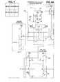
- FIG. 1illustrates a block diagram of a high performance asynchronous CMOS static memory (multi-port register file) in accordance with one embodiment of the present invention
- FIG. 2illustrates a block diagram of an alternate embodiment of a high performance asynchronous CMOS static memory (multi-port register file) including a column mux in accordance with one embodiment of the present invention
- FIG. 3illustrates one example of a storage device used in accordance with one embodiment of the present invention
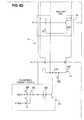
- FIG. 4comprising partial views 4 A, 4 B, 4 C, 4 D, 4 E and 4 F, illustrates a circuit diagram of a high performance asynchronous CMOS static memory (multi-port register file) including pull up and column muxes similar to that illustrated in FIG. 2 in accordance with one embodiment of the present invention
- FIG. 5illustrates a circuit diagram for a differential analog-style two-stage sense amplifier similar to that illustrated in FIG. 4 in accordance with one embodiment of the present invention
- FIG. 6illustrates a circuit diagram for a memory cell with a read port pair similar to that illustrated in FIG. 4 in accordance with one embodiment of the present invention
- FIG. 7illustrates a circuit diagram of a voltage reference circuit similar to that illustrated in FIG. 4 in accordance with one embodiment of the present invention
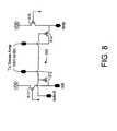
- FIG. 8illustrates a circuit diagram of a pull up & column mux similar to that illustrated in FIG. 4 in accordance with one embodiment of the present invention.
- FIG. 9illustrates a graph depicting the wave forms for the read path used in accordance with one embodiment of the present invention.
- One embodiment of the present inventionrelates to a high speed, high density differentially sensing register file memory or SRAM that operates synchronously or asynchronously with a low voltage power supply. It is contemplated that this embodiment reduces or eliminates noise effects on the bitlines, is more robust, uses less circuits, and takes up less space than currently known SRAMS.
- the register file memory or SRAMhas improved power dissipation (i.e., moderate) used in the 64 kb (kilo bit) or smaller range with a power supply voltage greater than 0 but less than about 2.00 volts, for example.
- the register file memorymay, in one embodiment, be a uni-directional multi-port memory (i.e., having dedicated write port(s) and dedicated read port(s) using a differential two-stage analog-style sense amp to sense a small bitline swing, about 100 millivolts (differentially) for example, located at the top rail of the voltage source.
- This register file memoryis generally used in applications in the 16 kb or smaller range with a power supply voltage which could be less than about 1.08 volts dissipating only 30 milliwatts of power (worst case) for a 128 channel configuration for example.
- This register file memoryreduces read access time to about 3 nanoseconds or less, may be considered more robust than previously known SRAM's, and eliminates noise effects on the bitlines that may falsely trip the sense amplifier.
- FIGS. 1 and 2A block diagram of two embodiments of the present invention are illustrated in FIGS. 1 and 2.
- the CMOS static memory or multi-port register file memorygenerally designated memory 10 and 110 in FIGS. 1 and 2 respectively, operates either synchronously or asynchronously and includes, for example, a register file memory cell 12 or 112 coupled to, connected to or otherwise electrically communicating directly or indirectly with a sense device or amplifier 20 or 120 (as illustrated in FIGS. 1 and 2) although other arrangements are contemplated.
- the memories 10 and 110store data (i.e., “words” and “bits per word”) provided, for example, during a write process.
- the sense device or amplifier 20 and 120sense a small bitline voltage swing, increasing performance of the memories 10 and 110 respectively.
- the register file memory cell 12comprises a read port pair 16 coupled to a storage element 14 .
- Differential sense amp 20is coupled to the register file memory cell 12 . More specifically sense amp 20 is coupled to the read port pair 16 .
- the voltage reference 18is coupled to the differential sense amp 20 , which in turn is coupled to the latched output circuit 22 having output 23 .
- the sense amp 20differentially senses a small bitline swing output by the read port pairs. In other words, sense amp 20 effectively senses a differential current on the local read bitlines rbit and rbitb, 27 .
- FIG. 1further illustrates a plurality of electrical connections or couplings. Electrical couplings wwd (write wordline), write bitlines (alternatively referred to as wbit and wbitb, 29 ) are shown coupled to storage element 14 . Storage element 14 is coupled to read port pair 16 via couplings or connections 28 . Rwd (read wordline) is illustrated coupled to read port pair 16 . In this embodiment, the memory 10 has no column mux (i.e., where each column is coupled to its own output channel), so read port pair 16 is coupled directly to the sense amp 20 via local read bitlines (alternatively referred to as rbit and rbitb, 27 ). Out or output line 23 is illustrated coupled or connected to latched output circuit 22 .
- the memory cellsare, in one embodiment, arranged in a plurality of rows and in at least one column, with each column coupled to a single output channel, storing recorded information.
- the read port pairsare coupled to the storage elements in an isolated manner (i.e., the read port pairs don't affect the static stability of the register file memory cell 12 ), enabling a plurality of memory cells to be arranged in such plurality of rows and in one (or more) columns, storing the recorded information.
- the memory stateis stored as a voltage differential within a bistable storage element 14 such as an inverter loop.
- bistable storage element 14such as an inverter loop.
- These storage devicesare either in a low or high stored memory state. If the storage device is in a low stored state, recording new and opposite information changes the storage device to a high stored state (logic “0” to logic “1” respectively). If the storage device is in a high stored state (logic 1), recording new and opposite information changes the storage device to a low stored state (logic 0).
- the presence or lack of a current at the sense amplifier 20determines the state contained within the selected memory location.
- the sense amplifier 20differentially senses the rbit and rbitb bitlines and outputs a corresponding voltage in order to communicate with the memory's output storage which requires full CMOS logic level input.
- the sense amplifiersenses a small predetermined bitline swing, say about 100 millivolts located at the top rail of the voltage supply for example. Having a small, predetermined bitline swing reduces the amount of time required to fully switch the highly capacitive bitlines.
- the bitline swingis at least a portion of the total voltage supply. Even with such a small bitline swing, it is sufficient for the two-stage sense amplifier to almost fully restore standard CMOS logic levels at the output of the sense amplifier.
- FIG. 2A block diagram of another embodiment of the present invention is illustrated in FIG. 2 .
- the memory 110 illustrated in FIG. 2includes a plurality of memory cells 112 each memory cell 112 comprising a read port pair 116 and a storage element 114 .
- Each memory cell 112is coupled to, connected or otherwise electrically communicates with a pull-up & column mux 124 and a column mux standby control 126 .
- the pull-up & column mux 124is coupled to the column mux & standby control 126 .
- Memory 110also includes a voltage reference 118 , which is coupled to each of the differential sense amps 120 for setting a constant current, which in turn is coupled to the latched output circuit 122 having an output 123 .
- the sense amp 120differentially senses a small bitline swing output by the read port pairs. In other words, sense amp 120 effectively senses a current by converting it to a voltage on the local read bitlines rbit and rbitb.
- memory 110includes electrical couplings wwd, wbit, wbitb, rwd, rbit, and rbitb similar to the embodiment illustrated in FIG. 1 . Couplings 128 and out 123 are illustrated.
- the read port pairs 116are coupled to the register file storage element 114 in an isolated manner, so that the read ports don't affect the static stability of the memory cell.
- the presence or lack of a current at the sense amplifier 120determines the data state stored in the selected memory location.
- the sense amplifier 120senses or detects the current and outputs a corresponding voltage in order to communicate with the memory's full CMOS output stage.
- a plurality of columns(configured as a multi-column mux register file memory) is contemplated as provided previously.
- Column muxingoptimizes memories with many words but with relatively few bits per word. From both a topological as well as a performance perspective, column muxing provides flexible embedded memory solutions.
- a pullup & column mux circuit(best viewed in FIG. 8) is used to implement such column muxing capability. This circuit is located conceptually between the register file memory cell 112 and the sense amplifier 120 . As should be apparent from the previous discussion and the figures, the number of column mux circuits is generally dependent on the number of columns and the number of bits per word.
- FIGS. 1 and 2reduce memory silicon area while improving speed in comparison to known SRAM memories or register files.
- Use of dedicated write and read ports in combination with differential two-stage sense amplifier(s)eliminates duplicate voltage circuits and/or reduces overall transistor count in the memory 10 and 110 resulting in a reduced amount of required silicon area.
- the illustrated embodimentalso optimizes memory read access time as the high transistor density translates to less interconnect capacitance and hence higher speed for a given or specific power level.
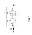
- FIG. 3one embodiment of the storage element 14 is illustrated, a 6T CMOS SRAM storage element for example.
- the 6T CMOS SRAM storage devicecomprises two P channel field-effect transistors (Pfets) 150 and 152 and four N channel field-effect transistors (Nfets) 154 , 156 , 158 and 160 .
- PfetsP channel field-effect transistors
- NfetsN channel field-effect transistors
- a Pfet transistoris turned on by a logic 0 at its gate and is adapted to pass or transmit a logic 1.
- An Nfet transistoris turned on by a logic 1 at its gate and is adapted to pass or transmit a logic 0.
- the storage deviceis either in a low or high stored memory state as provided above. If logic 0 is stored (i.e., storage device is in a low stored state) recording new and opposite information stores logic 1 (i.e., a high stored state). If a logic 1 is recorded on storage device (i.e., storage device is in a high stored state) recording new and opposite information records a logic 0 (i.e., changes the storage element data to a low stored state).
- FIG. 4A circuit diagram of SRAM or multiport register file 200 similar to memory 110 in FIG. 2 is illustrated in FIG. 4, comprising partial views 4 A, 4 B, 4 C, 4 D, 4 E and 4 F.
- the illustrated embodimentprovides improved power dissipation (i.e., moderate) used in the 64 kb (kilo bit) or smaller range with a power supply voltage greater than 0 but less than about 2.00 volts, for example.
- the register file memorymay, in one embodiment, be used in applications in the 16 kb or smaller range with a power supply voltage which could be less than about 1.08 volts without sacrificing significant speed from that typically expected, dissipating only 30 milliwatts of power (worst case) for a 128-channel configuration, for example.
- register file memory 200reduces read access time to about 3 nanoseconds or less, is more robust than previously known SRAM's and eliminates the noise effects on the bitlines that may falsely trip the sense amplifier.
- register file 200comprises read port pair 216 , pull-up & column mux 224 , column mux & standby control 226 , voltage reference 218 , differential analog-style two-stage sense amp 220 and latched output circuit 222 .
- FIG. 5A circuit diagram of one embodiment of a differential analog-style two-stage sense amp, similar to the differential sense amps 20 , 120 and 220 illustrated in FIGS. 1, 2 and 4 is illustrated in FIG. 5 .
- Sections A-Eare illustrated for discussion purposes only.
- Two sections, designated Sections A and Bare adapted to enhance the speed of the differential sense amp (alternatively referred to as amplifier enhancement devices).
- the differential sense ampoperates about 150 picoseconds faster than currently available sense amps due to the transistors of Sections A and B.
- Section Acomprises a Pfet transistor 349 which is coupled to VDD; transistors 310 , 314 , 324 and section C via its gate; and node imir, transistors 310 , 312 and 316 via its drain.
- Section Bcomprises a Pfet transistor 346 which is coupled to VDD; to ground via its gate; and transistor 312 via its drain.
- Section Athe first amplifier enhancing device, increases the DC voltage margin to the second stage, thus increasing functional reliability. More specifically, Section A, comprising Pfet transistor 349 , enables the output of the first stage of the differential analog-style two-stage sense amp to lower the absolute voltage (in the low state) than similarly known amplifier circuits. Referring to FIG. 5, transistor 349 turns on and tries to pull node imir up. When node imir pulls up, transistor 310 shuts off slightly, ultimately enabling the output of the first stage to fall further (as transistor 310 was put into a higher impedance mode). Enabling the output of the first stage to fall further than previously known amplifiers adds margin to the input of the second stage.
- the second amplifier enhancing device(which improves speed) is comprised of Pfet transistor 346 .
- Transistor 346(through transistor 312 ) turns on transistor 310 harder and stronger (than it would otherwise have been), causing transistor 310 to pull up the first stage output faster. Additionally, this “overdriving” of transistor 310 enables transistor 310 to be made smaller, thus lowering the capacitance on the first stage output node, which further improves the sense amp's speed.
- adding transistor 346 in line with transistor 312enables the output of the first stage to transition faster and, when coupled with the benefit provided via transistor 349 , adds noise margin to the second stage input.
- having transistors 346 and 349reduces effects due to process variation, reduces silicon area (due to transistor 310 shrinking considerably), and increases performance (speed).
- the differential analog-style two-stage state sense ampincludes a trip-level-shifted inverter designated Section C.
- the trip-level-shifted invertercomprises two transistors, a Pfet transistor 326 and an Nfet transistor 328 .
- Transistor 326is connected to VDD; transistors 328 , 324 , 310 , 314 and 349 via its gate; and node senout, transistors 328 , 330 , 332 , 342 and 340 through its drain.
- the trip-level-shifted inverteralso includes Nfet transistor 328 which is coupled to node senout and transistors 326 , 330 , 332 , 340 and 342 ; transistors 326 , 324 , 310 , 314 and 349 through its gate; and transistor 348 through its source. Shifting the second stage trip point higher and lowering the output voltage of the first stage adds operating margin to the sense amplifier.
- the differential analog-style, two-stage sense ampalso includes a power switch section designated Sections D and E.
- Section Dincludes two Nfet transistors 348 and 329 .
- Section Eincludes two Nfet transistors 308 and 318 .
- Sections D and Eturn power off to the sense amp.
- Nfet transistor 348is coupled to transistor 328 ; stbyb 2 through its gate; and transistor 329 through its source.
- Nfet transistor 329is coupled to transistor 348 and node ref via its gate; and to ground via its source.
- Nfet transistor 308is coupled to transistor differential pair 314 and 316 (node com); stbyb 1 through its gate; and transistor 318 through its source.
- Nfet transistor 318is coupled to transistor 308 and node ref via its gate; and to ground via its source.
- the illustrated differential sense ampalso requires a voltage reference 218 to establish a constant current.
- Section Ealong with this voltage reference, provides the circuitry necessary to generate the appropriate current for the differential amplifier.
- the differential analog-style two-stage sense ampincludes a first stage sense amp; comprising two Pfet transistors 310 and 312 , and two Nfet transistors 314 and 316 ; and a second stage sense amp, comprising transistors 326 , 328 , 348 and 329 (Sections C and D).
- Pfet transistor 310is coupled to VDD; node imir and transistors 349 , 316 and 312 via its gate; and transistors 349 , 324 , 314 and section C via its drain.
- Pfet transistor 312is coupled to transistor 346 ; node imir, transistors 310 , 316 , 349 and its own drain via its gate; and to transistors 316 , 310 , 349 and its own gate via its drain.
- Nfet transistor 314is coupled to transistors 310 , 349 , 324 and Section C; transistors 320 and node sbit through its gate; and node corn; transistors 308 and 316 through its source.
- Nfet transistor 316is coupled to transistors 312 , 310 and 349 ; to transistors 322 and node sbitb through its gate; and node corn; transistors 308 and 314 through its source.
- Transistors 310 , 312 , 314 and 316 , along with the transistors in Section E ( 308 and 318 )amplify the signals input on the sbit and sbitb nodes.
- the resultant outputis passed to the second stage for further amplification.
- Transistors 358 , 360 , 354 , 356 , 350 , 352 , 324 , 320 and 322provide the necessary logic to correctly power down the analog-style two-stage sense amp using the standby (stby and/or stbyb) signal(s).
- Transistors 330 , 332 , 334 , 336 , 338 , 340 , 342 and 334form the necessary circuits to perform the correct output logic polarity as well as drive current and (power down) latch function.
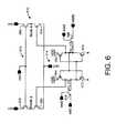
- FIG. 6illustrates one embodiment of a memory cell 612 similar to the register file memory cell 12 and 112 provided previously.
- the memory cell 612comprises storage portion 614 and read port portion 613 .
- the storage portioncomprises two Pfet transistors 684 and 682 and four Nfet transistors 670 , 672 , 674 and 688 .
- the read port portion 613comprises two read port pairs (dedicated read port(s)) coupled to the 6T storage element 614 , rbit and rbitb, where transistors 676 and 686 comprise one read port pair connected or coupled to each other at node a and transistors 680 and 678 comprise a second read port pair connected or coupled to each other at node b.
- transistors 674 and 688comprise the dedicated write port pair actuated by a signal on wwd (write wordline) and communicating with wbit and wbitb (the write bitlines). While one embodiment of the present invention includes one read and write port, one, two or more (i.e., a plurality) read and write ports are contemplated.
- the transistors in at least one, but generally both, of the read port pairsdiffer in size. More specifically, transistor 686 is larger than transistor 676 and transistor 678 is larger than transistor 680 . In one embodiment of the present invention, transistors 686 and 678 are about equal in size and transistors 676 and 680 are about equal in size, although other embodiments are contemplated where transistors 686 and 678 differ in size although they are still larger than transistors 676 and 680 (which may also differ in size depending on the memory requirements).
- transistors 686 and 678 larger than transistors 676 and 680 respectivelytranslates into greater speed for the memory cell. More specifically, having transistors 686 and 678 larger than transistors 676 and 680 respectively, pulls nodes a and b lower than comparable memory cells, creating a bigger gate to source voltage for a given transistor. This increases the current in the selected read port pair, which causes the associated bitline to discharge faster for a given silicon area.
- transistors 676 and 680 in size in comparison to similar memory cellsalso translates into greater speed for the memory cell. More specifically, reducing the size of transistors 676 and 680 reduces capacitance on the associated bitlines. Reducing capacitance on the bitlines in combination with a larger gate-to-source voltage for transistors 676 and 680 , increases current per capacitance on the bitlines.
- FIG. 7illustrates one embodiment of the voltage reference 718 similar to voltage reference 18 and 118 provided previously.
- the voltage reference 718includes one Pfet transistor 790 and three Nfet transistors 792 , 794 , and 796 .
- Transistor 790is coupled to VDD; ground via its gate; and to resistor R 1 and transistor 792 through its drain.
- Transistor 792is coupled to resistor R 1 and node ref; the other side of resistor R 1 and transistor 790 through its gate; and transistor 794 through its source.
- Transistor 794is coupled to transistor 792 ; node stbyb through its gate; and transistor 796 through its source.
- Transistor 796is coupled to transistor 794 and its gate; transistor 794 and itself through its gate; and to ground via its source.
- the pull-up & column mux(similar to the pull-up and column mux 124 illustrated in FIG. 2) is adapted to manipulate a non-performance optimized logical memory array into a more practical physical memory array implementation, by selecting one column from a plurality of columns.
- the column muxenables a plurality of columns to share outputs, where at least one column may be selected from the plurality of columns. If the plurality of columns did not share outputs, each column would require its own output.
- FIG. 8represents one embodiment of the circuitry that may be used to implement column muxing capability.
- This column mux circuit 800is located conceptually between the register file memory cells and the differential sense amp.
- the illustrated column mux circuit 800illustrates only one example of column muxing.
- the circuitincludes four Pfet transistors 810 , 812 , 814 and 816 .
- Transistors 812 and 814are coupled to and controlled by the column mux & standby control circuitry through their gate and labeled “select” in this Figure (similar to the column mux & standby control 226 illustrated in FIG. 4 ); to the differential sense amp through their drains; while their sources are separately connected to rbit and rbitb.
- the number of column mux circuitsis generally dependent on the number of columns. If the memory only employs one or two columns, a column mux circuit is not employed. However, the use of a column mux is more applicable to shift memories with many words and few bits per word into a physical array with fewer rows and more columns.
- the pull-upsare all active all the time, pulling up the bitlines.
- One of the addresses (designated R 1 , R 2 and R 3 ) in FIG. 4is selected. While only three addresses (wordlines) are illustrated, a plurality of addresses (wordlines) are contemplated. Selecting one of the wordlines effectively selects one side or the other of the storage element in each selected column.
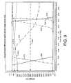
- FIG. 9Waveforms of one embodiment of the read path are illustrated in FIG. 9 .
- the large dashed line 912represents the voltage change for a selecting address over time.
- the voltage waveforms of 912switches as does the deselecting address depicted by solid line 926 .
- the selected address line ( 912 for example)goes high as the deselected address line ( 926 for example) goes low. This begins the read cycle at about 33.1 nanoseconds as shown.
- This new address selection(more specifically the selection of one wordline and the deselection of another wordline) causes a series of events to begin.
- the short dashed line 914represents the voltage change for rbit over time while its counterpart short dashed line 916 (rbitb) can be seen operating differentially with about 140 millivolts of swing.
- one of the bitlinesgoes high (rbit for example as illustrated by line 914 ) while the voltage on the other bitline goes low (rbitb for example as illustrated by line 916 ).
- the alternating large and small dashed line 920represents the voltage of the trip point for the second stage of the sense amp.
- the trip-level-shifted invertershifts the trip point up in comparison to a standard logic inverter. In this embodiment and at this simulated operating point, the trip level is at about 620 millivolts.
- Large dashed line 918represents the output of first stage (and the input to the second stage) of the sense amp, which is shifted down (increasing the margin on the low side) as provided previously.
- the voltage change on the bitlines (rbit and rbitb represented by lines 914 and 916 )causes the voltage on 918 to change (drop), crossing the voltage-shifted trip-level of the second stage amplifier.
- the alternating large and small dashed lines 922 and 924respectively represent the voltage change for senout and the output of the memory over time. Of course, similar operation will occur in the opposite direction, where the opposite data state is read from the memory contents.
- any number of sense amplifiersis contemplated, depending on the number of output channels, where one sense amplifier is employed for each output channel. It should be appreciated that there is a physical memory array and a logical memory array.
- the physical memory arrayis denoted by the terms rows and columns while the logical memory array uses the terms “words” and “bits per word”.
- the number of bits per worddetermines the number of output channels and hence the number of sense amplifiers 20 , 120 .
- Bits per word and output channelshave a one to one correlation. For example, if a particular memory has 16 bits per word, it has 16 outputs and therefore 16 sense amplifiers. Column muxing enables one to manipulate a non-performance optimized logical memory array into a more practical physical memory array implementation.
Landscapes
- Engineering & Computer Science (AREA)
- Microelectronics & Electronic Packaging (AREA)
- Computer Hardware Design (AREA)
- Static Random-Access Memory (AREA)
- Dram (AREA)
Abstract
Description
Claims (25)
Priority Applications (10)
| Application Number | Priority Date | Filing Date | Title |
|---|---|---|---|
| US10/012,858US6639866B2 (en) | 2000-11-03 | 2001-11-03 | Very small swing high performance asynchronous CMOS static memory (multi-port register file) with power reducing column multiplexing scheme |
| DE60119583TDE60119583T2 (en) | 2000-11-03 | 2001-11-05 | CMOS memory with small fluctuating voltages and low operating voltage |
| EP01989977AEP1374248B1 (en) | 2000-11-03 | 2001-11-05 | Very small swing and low voltage cmos static memory |
| PCT/US2001/046942WO2002043072A2 (en) | 2000-11-03 | 2001-11-05 | Very small swing and low voltage cmos static memory |
| US10/352,417US6898103B2 (en) | 2000-11-03 | 2003-01-28 | Memory cell with fuse element |
| US10/679,547US6822918B2 (en) | 2000-11-03 | 2003-10-06 | Very small swing high performance asynchronous CMOS static memory (multi-port register file) with power reducing column multiplexing scheme |
| US10/764,239US6903993B2 (en) | 2000-11-03 | 2004-01-22 | Memory cell with fuse element |
| US10/996,140US7251175B2 (en) | 2000-11-03 | 2004-11-23 | Very small swing high performance asynchronous CMOS static memory (multi-port register file) with power reducing column multiplexing scheme |
| US11/777,054US7639549B2 (en) | 2000-11-03 | 2007-07-12 | Very small swing high performance asynchronous CMOS static memory (multi-port register file) with power reducing column multiplexing scheme |
| US12/617,570US7986570B2 (en) | 2000-11-03 | 2009-11-12 | Very small swing high performance asynchronous CMOS static memory (multi-port register file) with power reducing column multiplexing scheme |
Applications Claiming Priority (2)
| Application Number | Priority Date | Filing Date | Title |
|---|---|---|---|
| US24591300P | 2000-11-03 | 2000-11-03 | |
| US10/012,858US6639866B2 (en) | 2000-11-03 | 2001-11-03 | Very small swing high performance asynchronous CMOS static memory (multi-port register file) with power reducing column multiplexing scheme |
Related Child Applications (3)
| Application Number | Title | Priority Date | Filing Date |
|---|---|---|---|
| US10/025,132Continuation-In-PartUS6525955B1 (en) | 2000-11-03 | 2001-12-18 | Memory cell with fuse element |
| US10/352,417Continuation-In-PartUS6898103B2 (en) | 2000-11-03 | 2003-01-28 | Memory cell with fuse element |
| US10/679,547ContinuationUS6822918B2 (en) | 2000-11-03 | 2003-10-06 | Very small swing high performance asynchronous CMOS static memory (multi-port register file) with power reducing column multiplexing scheme |
Publications (2)
| Publication Number | Publication Date |
|---|---|
| US20020125585A1 US20020125585A1 (en) | 2002-09-12 |
| US6639866B2true US6639866B2 (en) | 2003-10-28 |
Family
ID=26684094
Family Applications (5)
| Application Number | Title | Priority Date | Filing Date |
|---|---|---|---|
| US10/012,858Expired - LifetimeUS6639866B2 (en) | 2000-11-03 | 2001-11-03 | Very small swing high performance asynchronous CMOS static memory (multi-port register file) with power reducing column multiplexing scheme |
| US10/679,547Expired - LifetimeUS6822918B2 (en) | 2000-11-03 | 2003-10-06 | Very small swing high performance asynchronous CMOS static memory (multi-port register file) with power reducing column multiplexing scheme |
| US10/996,140Expired - LifetimeUS7251175B2 (en) | 2000-11-03 | 2004-11-23 | Very small swing high performance asynchronous CMOS static memory (multi-port register file) with power reducing column multiplexing scheme |
| US11/777,054Expired - Fee RelatedUS7639549B2 (en) | 2000-11-03 | 2007-07-12 | Very small swing high performance asynchronous CMOS static memory (multi-port register file) with power reducing column multiplexing scheme |
| US12/617,570Expired - Fee RelatedUS7986570B2 (en) | 2000-11-03 | 2009-11-12 | Very small swing high performance asynchronous CMOS static memory (multi-port register file) with power reducing column multiplexing scheme |
Family Applications After (4)
| Application Number | Title | Priority Date | Filing Date |
|---|---|---|---|
| US10/679,547Expired - LifetimeUS6822918B2 (en) | 2000-11-03 | 2003-10-06 | Very small swing high performance asynchronous CMOS static memory (multi-port register file) with power reducing column multiplexing scheme |
| US10/996,140Expired - LifetimeUS7251175B2 (en) | 2000-11-03 | 2004-11-23 | Very small swing high performance asynchronous CMOS static memory (multi-port register file) with power reducing column multiplexing scheme |
| US11/777,054Expired - Fee RelatedUS7639549B2 (en) | 2000-11-03 | 2007-07-12 | Very small swing high performance asynchronous CMOS static memory (multi-port register file) with power reducing column multiplexing scheme |
| US12/617,570Expired - Fee RelatedUS7986570B2 (en) | 2000-11-03 | 2009-11-12 | Very small swing high performance asynchronous CMOS static memory (multi-port register file) with power reducing column multiplexing scheme |
Country Status (4)
| Country | Link |
|---|---|
| US (5) | US6639866B2 (en) |
| EP (1) | EP1374248B1 (en) |
| DE (1) | DE60119583T2 (en) |
| WO (1) | WO2002043072A2 (en) |
Cited By (5)
| Publication number | Priority date | Publication date | Assignee | Title |
|---|---|---|---|---|
| US20050058002A1 (en)* | 2003-09-16 | 2005-03-17 | Oki Electric Industry Co., Ltd. | Multi-port semiconductor memory |
| US6873565B1 (en)* | 2003-10-10 | 2005-03-29 | Hewlett-Packard Development Company, L.P. | Dual-ported read SRAM cell with improved soft error immunity |
| US20050091477A1 (en)* | 2000-11-03 | 2005-04-28 | Mark Slamowitz | Very small swing high performance asynchronous CMOS static memory (multi-port register file) with power reducing column multiplexing scheme |
| US20060134631A1 (en)* | 1996-01-09 | 2006-06-22 | Krokan Hans E | Novel DNA glycosylases and their use |
| US20110194370A1 (en)* | 2010-02-10 | 2011-08-11 | Shinye Shiu | Memory Having Asynchronous Read With Fast Read Output |
Families Citing this family (21)
| Publication number | Priority date | Publication date | Assignee | Title |
|---|---|---|---|---|
| US6525955B1 (en)* | 2001-12-18 | 2003-02-25 | Broadcom Corporation | Memory cell with fuse element |
| FR2871922A1 (en)* | 2004-06-17 | 2005-12-23 | St Microelectronics Sa | LIVING MEMORY CELL WITH REDUCED DIMENSIONS AND COMPLEXITY |
| KR100745368B1 (en)* | 2005-11-22 | 2007-08-02 | 삼성전자주식회사 | Semiconductor memory device with improved data input / output path |
| CN101449256B (en) | 2006-04-12 | 2013-12-25 | 索夫特机械公司 | Apparatus and method for processing instruction matrix specifying parallel and dependent operations |
| EP2527972A3 (en)* | 2006-11-14 | 2014-08-06 | Soft Machines, Inc. | Apparatus and method for processing complex instruction formats in a multi- threaded architecture supporting various context switch modes and virtualization schemes |
| US7746713B2 (en)* | 2007-09-12 | 2010-06-29 | Massachusetts Institute Of Technology | High density 45 nm SRAM using small-signal non-strobed regenerative sensing |
| US7961499B2 (en)* | 2009-01-22 | 2011-06-14 | Qualcomm Incorporated | Low leakage high performance static random access memory cell using dual-technology transistors |
| TWI419173B (en)* | 2009-07-31 | 2013-12-11 | Univ Nat Chiao Tung | Static random access memory device |
| TWI453749B (en)* | 2010-02-05 | 2014-09-21 | Univ Nat Chiao Tung | Subthreshold multi-port register file design |
| TWI455148B (en)* | 2010-12-13 | 2014-10-01 | Vanguard Int Semiconduct Corp | Integrated device for accessing multi-port input read/write event |
| US20120235708A1 (en)* | 2011-03-16 | 2012-09-20 | Mark Slamowitz | Method and System for High Speed Differential Synchronous Sense Amplifier |
| KR101966712B1 (en) | 2011-03-25 | 2019-04-09 | 인텔 코포레이션 | Memory fragments for supporting code block execution by using virtual cores instantiated by partitionable engines |
| US8593896B2 (en)* | 2011-03-30 | 2013-11-26 | Taiwan Semiconductor Manufacturing Company, Ltd. | Differential read write back sense amplifier circuits and methods |
| US8522178B2 (en)* | 2011-09-07 | 2013-08-27 | Apple Inc. | Re-modeling a memory array for accurate timing analysis |
| KR20130130478A (en)* | 2012-05-22 | 2013-12-02 | 삼성전자주식회사 | Input buffer |
| US10140138B2 (en) | 2013-03-15 | 2018-11-27 | Intel Corporation | Methods, systems and apparatus for supporting wide and efficient front-end operation with guest-architecture emulation |
| WO2014151043A1 (en) | 2013-03-15 | 2014-09-25 | Soft Machines, Inc. | A method for emulating a guest centralized flag architecture by using a native distributed flag architecture |
| US9691462B2 (en) | 2014-09-27 | 2017-06-27 | Qualcomm Incorporated | Latch offset cancelation for magnetoresistive random access memory |
| US9373388B1 (en)* | 2015-04-29 | 2016-06-21 | Qualcomm Incorporated | Sense amplifier with pulsed control for pull-up transistors |
| US11087800B1 (en)* | 2020-04-10 | 2021-08-10 | Sandisk Technologies Llc | Sense amplifier architecture providing small swing voltage sensing |
| US11955169B2 (en)* | 2021-03-23 | 2024-04-09 | Qualcomm Incorporated | High-speed multi-port memory supporting collision |
Citations (10)
| Publication number | Priority date | Publication date | Assignee | Title |
|---|---|---|---|---|
| US4580245A (en) | 1983-07-28 | 1986-04-01 | Sperry Corporation | Complementary metal oxide semiconductor dual port random access memory cell |
| US4843264A (en)* | 1987-11-25 | 1989-06-27 | Visic, Inc. | Dynamic sense amplifier for CMOS static RAM |
| US4933899A (en)* | 1989-02-01 | 1990-06-12 | Cypress Semiconductor | Bi-CMOS semiconductor memory cell |
| US5260908A (en)* | 1991-04-24 | 1993-11-09 | Kabushiki Kaisha Toshiba | Multiport memory device |
| US5477489A (en)* | 1995-03-20 | 1995-12-19 | Exponential Technology, Inc. | High-stability CMOS multi-port register file memory cell with column isolation and current-mirror row line driver |
| US5590087A (en) | 1993-05-05 | 1996-12-31 | Hewlett-Packard Company | Multi-ported data storage device with improved cell stability |
| US5608681A (en) | 1996-01-22 | 1997-03-04 | Lsi Logic Corporation | Fast memory sense system |
| US5640356A (en) | 1995-12-29 | 1997-06-17 | Cypress Semiconductor Corp. | Two-stage differential sense amplifier with positive feedback in the first and second stages |
| JPH09186535A (en) | 1995-12-27 | 1997-07-15 | Toshiba Microelectron Corp | Differential input type sense amplifier circuit |
| US6222777B1 (en)* | 1999-04-09 | 2001-04-24 | Sun Microsystems, Inc. | Output circuit for alternating multiple bit line per column memory architecture |
Family Cites Families (25)
| Publication number | Priority date | Publication date | Assignee | Title |
|---|---|---|---|---|
| US2829333A (en)* | 1955-04-22 | 1958-04-01 | Sperry Gyroscope Co Ltd | Constant-frequency alternating-current generators |
| US2854617A (en)* | 1957-01-24 | 1958-09-30 | Siegler Corp | Frequency control apparatus for alternators |
| GB1448990A (en)* | 1972-12-22 | 1976-09-08 | Nat Res Dev | Roatary and linear electric machines |
| US4019104A (en)* | 1974-03-26 | 1977-04-19 | Parker Louis W | Variable speed induction motor |
| US4305001A (en)* | 1979-02-26 | 1981-12-08 | Lima Electric Company, Inc. | Constant frequency alternator |
| US4229689A (en)* | 1979-11-05 | 1980-10-21 | Nickoladze Leo G | AC Synchronized generator |
| US4472673A (en)* | 1982-04-15 | 1984-09-18 | Energia Andina Ltda. | Rotating electric machine with speed/frequency control |
| US4563753A (en)* | 1984-09-04 | 1986-01-07 | Motorola, Inc. | Circuit for reducing degradation of voltage differential in a memory |
| US4625160A (en)* | 1984-12-17 | 1986-11-25 | Sundstrand Corporation | Variable speed constant frequency generating system |
| US4701691A (en)* | 1985-05-14 | 1987-10-20 | Nickoladze Leo G | Synchronous generators |
| US4817051A (en)* | 1987-07-02 | 1989-03-28 | Fairchild Semiconductor Corporation | Expandable multi-port random access memory |
| US5587643A (en)* | 1988-07-12 | 1996-12-24 | Heller Dejulio Corporation | Rotary induction machine having control of secondary winding impedance |
| US5274291A (en)* | 1990-01-08 | 1993-12-28 | Clarke Patrick W | Rotary transformer with multiple angularly adjustable stators |
| US5003509A (en)* | 1990-03-27 | 1991-03-26 | National Semiconductor Corp. | Multi-port, bipolar-CMOS memory cell |
| DE69100430T2 (en)* | 1990-05-26 | 1994-04-28 | Satake Eng Co Ltd | Synchronous induction motor with double stator. |
| JP3033621B2 (en)* | 1991-08-28 | 2000-04-17 | 株式会社佐竹製作所 | Brushless induction synchronous motor |
| US5525894A (en)* | 1992-08-03 | 1996-06-11 | Heller-Dejulio Corporation | Rotary induction generator adapted to be driven by a prime mover for generating electric power |
| US5418446A (en)* | 1993-05-10 | 1995-05-23 | Hallidy; William M. | Variable speed constant frequency synchronous electric power generating system and method of using same |
| EP0681293B1 (en)* | 1994-05-03 | 2001-03-28 | STMicroelectronics S.r.l. | Sense amplifier with hysteresis |
| US5521874A (en)* | 1994-12-14 | 1996-05-28 | Sun Microsystems, Inc. | High speed differential to single ended sense amplifier |
| JP3069263B2 (en)* | 1995-01-18 | 2000-07-24 | 株式会社村上開明堂 | Connection structure between drive unit and harness in electric remote control mirror |
| US5724299A (en)* | 1996-04-30 | 1998-03-03 | Sun Microsystems, Inc. | Multiport register file memory using small voltage swing for write operation |
| US6091627A (en)* | 1998-09-16 | 2000-07-18 | Lucent Technologies, Inc. | Message box memory cell for two-side asynchronous access |
| US6639866B2 (en)* | 2000-11-03 | 2003-10-28 | Broadcom Corporation | Very small swing high performance asynchronous CMOS static memory (multi-port register file) with power reducing column multiplexing scheme |
| US6519204B2 (en)* | 2000-11-03 | 2003-02-11 | Broadcom Corporation | Very small swing high performance CMOS static memory (multi-port register file) with power reducing column multiplexing scheme |
- 2001
- 2001-11-03USUS10/012,858patent/US6639866B2/ennot_activeExpired - Lifetime
- 2001-11-05DEDE60119583Tpatent/DE60119583T2/ennot_activeExpired - Lifetime
- 2001-11-05EPEP01989977Apatent/EP1374248B1/ennot_activeExpired - Lifetime
- 2001-11-05WOPCT/US2001/046942patent/WO2002043072A2/enactiveIP Right Grant
- 2003
- 2003-10-06USUS10/679,547patent/US6822918B2/ennot_activeExpired - Lifetime
- 2004
- 2004-11-23USUS10/996,140patent/US7251175B2/ennot_activeExpired - Lifetime
- 2007
- 2007-07-12USUS11/777,054patent/US7639549B2/ennot_activeExpired - Fee Related
- 2009
- 2009-11-12USUS12/617,570patent/US7986570B2/ennot_activeExpired - Fee Related
Patent Citations (10)
| Publication number | Priority date | Publication date | Assignee | Title |
|---|---|---|---|---|
| US4580245A (en) | 1983-07-28 | 1986-04-01 | Sperry Corporation | Complementary metal oxide semiconductor dual port random access memory cell |
| US4843264A (en)* | 1987-11-25 | 1989-06-27 | Visic, Inc. | Dynamic sense amplifier for CMOS static RAM |
| US4933899A (en)* | 1989-02-01 | 1990-06-12 | Cypress Semiconductor | Bi-CMOS semiconductor memory cell |
| US5260908A (en)* | 1991-04-24 | 1993-11-09 | Kabushiki Kaisha Toshiba | Multiport memory device |
| US5590087A (en) | 1993-05-05 | 1996-12-31 | Hewlett-Packard Company | Multi-ported data storage device with improved cell stability |
| US5477489A (en)* | 1995-03-20 | 1995-12-19 | Exponential Technology, Inc. | High-stability CMOS multi-port register file memory cell with column isolation and current-mirror row line driver |
| JPH09186535A (en) | 1995-12-27 | 1997-07-15 | Toshiba Microelectron Corp | Differential input type sense amplifier circuit |
| US5640356A (en) | 1995-12-29 | 1997-06-17 | Cypress Semiconductor Corp. | Two-stage differential sense amplifier with positive feedback in the first and second stages |
| US5608681A (en) | 1996-01-22 | 1997-03-04 | Lsi Logic Corporation | Fast memory sense system |
| US6222777B1 (en)* | 1999-04-09 | 2001-04-24 | Sun Microsystems, Inc. | Output circuit for alternating multiple bit line per column memory architecture |
Cited By (16)
| Publication number | Priority date | Publication date | Assignee | Title |
|---|---|---|---|---|
| US20060134631A1 (en)* | 1996-01-09 | 2006-06-22 | Krokan Hans E | Novel DNA glycosylases and their use |
| US7662601B2 (en) | 1996-01-09 | 2010-02-16 | Krokan Hans E | DNA glycosylases and their use |
| US20080089144A1 (en)* | 2000-11-03 | 2008-04-17 | Mark Slamowitz | Very Small Swing High Performance Asynchronous CMOS Static Memory (Multi-Port Register File) With Power Reducing Column Multiplexing Scheme |
| US7639549B2 (en)* | 2000-11-03 | 2009-12-29 | Broadcom Corporation | Very small swing high performance asynchronous CMOS static memory (multi-port register file) with power reducing column multiplexing scheme |
| US7986570B2 (en)* | 2000-11-03 | 2011-07-26 | Broadcom Corporation | Very small swing high performance asynchronous CMOS static memory (multi-port register file) with power reducing column multiplexing scheme |
| US20100177581A1 (en)* | 2000-11-03 | 2010-07-15 | Mark Slamowitz | Very Small Swing High Performance Asynchronous CMOS Static Memory (Multi-Port Register File) With Power Reducing Column Multiplexing Scheme |
| US20050091477A1 (en)* | 2000-11-03 | 2005-04-28 | Mark Slamowitz | Very small swing high performance asynchronous CMOS static memory (multi-port register file) with power reducing column multiplexing scheme |
| US7251175B2 (en)* | 2000-11-03 | 2007-07-31 | Broadcom Corporation | Very small swing high performance asynchronous CMOS static memory (multi-port register file) with power reducing column multiplexing scheme |
| US20070070779A1 (en)* | 2003-09-16 | 2007-03-29 | Koichi Morikawa | Multi-port semiconductor memory |
| US7477566B2 (en) | 2003-09-16 | 2009-01-13 | Oki Semiconductor Co., Ltd. | Multi-port semiconductor memory |
| US20050058002A1 (en)* | 2003-09-16 | 2005-03-17 | Oki Electric Industry Co., Ltd. | Multi-port semiconductor memory |
| US7170814B2 (en)* | 2003-09-16 | 2007-01-30 | Oki Electric Industry Co., Ltd. | Multi-port semiconductor memory |
| US6873565B1 (en)* | 2003-10-10 | 2005-03-29 | Hewlett-Packard Development Company, L.P. | Dual-ported read SRAM cell with improved soft error immunity |
| US20050078543A1 (en)* | 2003-10-10 | 2005-04-14 | Riedlinger Reid James | Dual-ported read sram cell with improved soft error immunity |
| US20110194370A1 (en)* | 2010-02-10 | 2011-08-11 | Shinye Shiu | Memory Having Asynchronous Read With Fast Read Output |
| US8493811B2 (en)* | 2010-02-10 | 2013-07-23 | Apple Inc. | Memory having asynchronous read with fast read output |
Also Published As
| Publication number | Publication date |
|---|---|
| DE60119583T2 (en) | 2007-05-10 |
| US20040066687A1 (en) | 2004-04-08 |
| US20020125585A1 (en) | 2002-09-12 |
| WO2002043072A3 (en) | 2003-04-24 |
| EP1374248A2 (en) | 2004-01-02 |
| US6822918B2 (en) | 2004-11-23 |
| WO2002043072A2 (en) | 2002-05-30 |
| US7639549B2 (en) | 2009-12-29 |
| DE60119583D1 (en) | 2006-06-14 |
| US7251175B2 (en) | 2007-07-31 |
| EP1374248B1 (en) | 2006-05-10 |
| US20100177581A1 (en) | 2010-07-15 |
| US7986570B2 (en) | 2011-07-26 |
| US20080089144A1 (en) | 2008-04-17 |
| US20050091477A1 (en) | 2005-04-28 |
Similar Documents
| Publication | Publication Date | Title |
|---|---|---|
| US7639549B2 (en) | Very small swing high performance asynchronous CMOS static memory (multi-port register file) with power reducing column multiplexing scheme | |
| US7821858B2 (en) | eDRAM hierarchical differential sense AMP | |
| US5986914A (en) | Active hierarchical bitline memory architecture | |
| US6519204B2 (en) | Very small swing high performance CMOS static memory (multi-port register file) with power reducing column multiplexing scheme | |
| US6711051B1 (en) | Static RAM architecture with bit line partitioning | |
| US7564729B2 (en) | Differential and hierarchical sensing for memory circuits | |
| US6449202B1 (en) | DRAM direct sensing scheme | |
| KR910009442B1 (en) | Semiconductor memory | |
| CN113823342B (en) | Semiconductor integrated circuits and memories | |
| US20060039176A1 (en) | Memory cell | |
| WO2007051764A1 (en) | System and method for capacitive mis-match bit-line sensing | |
| CN109859791B (en) | 9-pipe SRAM (static random Access memory) storage unit with full-isolation structure and read-write operation method thereof | |
| EP1661137B1 (en) | Low voltage operation dram control circuits | |
| US5696724A (en) | Sense amplifier | |
| US6944066B1 (en) | Low voltage data path and current sense amplifier | |
| US20030063511A1 (en) | Leakage-tolerant memory arrangements | |
| US7336553B2 (en) | Enhanced sensing in a hierarchical memory architecture | |
| US6816401B2 (en) | Static random access memory (SRAM) without precharge circuitry | |
| US7525859B2 (en) | Sense amplifier of semiconductor memory device | |
| EP0622801A2 (en) | Hierarchical bitline memory architecture | |
| US6141235A (en) | Stacked cache memory system and method |
Legal Events
| Date | Code | Title | Description |
|---|---|---|---|
| AS | Assignment | Owner name:BROADCOM CORPORATION, CALIFORNIA Free format text:ASSIGNMENT OF ASSIGNORS INTEREST;ASSIGNORS:SLAMOWITZ, MARK;SMITH, DOUGLAS D.;KNEBELSBERGER, DAVID W.;AND OTHERS;REEL/FRAME:012614/0008 Effective date:20011102 | |
| STCF | Information on status: patent grant | Free format text:PATENTED CASE | |
| FPAY | Fee payment | Year of fee payment:4 | |
| FPAY | Fee payment | Year of fee payment:8 | |
| FPAY | Fee payment | Year of fee payment:12 | |
| SULP | Surcharge for late payment | Year of fee payment:11 | |
| AS | Assignment | Owner name:BANK OF AMERICA, N.A., AS COLLATERAL AGENT, NORTH CAROLINA Free format text:PATENT SECURITY AGREEMENT;ASSIGNOR:BROADCOM CORPORATION;REEL/FRAME:037806/0001 Effective date:20160201 Owner name:BANK OF AMERICA, N.A., AS COLLATERAL AGENT, NORTH Free format text:PATENT SECURITY AGREEMENT;ASSIGNOR:BROADCOM CORPORATION;REEL/FRAME:037806/0001 Effective date:20160201 | |
| AS | Assignment | Owner name:AVAGO TECHNOLOGIES GENERAL IP (SINGAPORE) PTE. LTD., SINGAPORE Free format text:ASSIGNMENT OF ASSIGNORS INTEREST;ASSIGNOR:BROADCOM CORPORATION;REEL/FRAME:041706/0001 Effective date:20170120 Owner name:AVAGO TECHNOLOGIES GENERAL IP (SINGAPORE) PTE. LTD Free format text:ASSIGNMENT OF ASSIGNORS INTEREST;ASSIGNOR:BROADCOM CORPORATION;REEL/FRAME:041706/0001 Effective date:20170120 | |
| AS | Assignment | Owner name:BROADCOM CORPORATION, CALIFORNIA Free format text:TERMINATION AND RELEASE OF SECURITY INTEREST IN PATENTS;ASSIGNOR:BANK OF AMERICA, N.A., AS COLLATERAL AGENT;REEL/FRAME:041712/0001 Effective date:20170119 | |
| AS | Assignment | Owner name:AVAGO TECHNOLOGIES INTERNATIONAL SALES PTE. LIMITE Free format text:MERGER;ASSIGNOR:AVAGO TECHNOLOGIES GENERAL IP (SINGAPORE) PTE. LTD.;REEL/FRAME:047195/0026 Effective date:20180509 | |
| AS | Assignment | Owner name:AVAGO TECHNOLOGIES INTERNATIONAL SALES PTE. LIMITE Free format text:CORRECTIVE ASSIGNMENT TO CORRECT THE EFFECTIVE DATE OF MERGER PREVIOUSLY RECORDED ON REEL 047195 FRAME 0026. ASSIGNOR(S) HEREBY CONFIRMS THE MERGER;ASSIGNOR:AVAGO TECHNOLOGIES GENERAL IP (SINGAPORE) PTE. LTD.;REEL/FRAME:047477/0423 Effective date:20180905 |