US6639291B1 - Spin dependent tunneling barriers doped with magnetic particles - Google Patents
Spin dependent tunneling barriers doped with magnetic particlesDownload PDFInfo
- Publication number
- US6639291B1 US6639291B1US10/071,796US7179602AUS6639291B1US 6639291 B1US6639291 B1US 6639291B1US 7179602 AUS7179602 AUS 7179602AUS 6639291 B1US6639291 B1US 6639291B1
- Authority
- US
- United States
- Prior art keywords
- layer
- ferromagnetic
- magnetic moment
- tunnel barrier
- ferromagnetic layer
- Prior art date
- Legal status (The legal status is an assumption and is not a legal conclusion. Google has not performed a legal analysis and makes no representation as to the accuracy of the status listed.)
- Expired - Lifetime, expires
Links
- 230000004888barrier functionEffects0.000titleclaimsabstractdescription65
- 230000005641tunnelingEffects0.000titleabstractdescription18
- 230000001419dependent effectEffects0.000titleabstractdescription7
- 239000006249magnetic particleSubstances0.000titledescription35
- 230000005294ferromagnetic effectEffects0.000claimsabstractdescription92
- 239000002245particleSubstances0.000claimsabstractdescription20
- 230000004044responseEffects0.000claimsabstractdescription14
- 230000005291magnetic effectEffects0.000claimsdescription62
- 230000005415magnetizationEffects0.000claimsdescription17
- PXHVJJICTQNCMI-UHFFFAOYSA-NNickelChemical compound[Ni]PXHVJJICTQNCMI-UHFFFAOYSA-N0.000claimsdescription16
- XEEYBQQBJWHFJM-UHFFFAOYSA-NIronChemical compound[Fe]XEEYBQQBJWHFJM-UHFFFAOYSA-N0.000claimsdescription14
- 229910052759nickelInorganic materials0.000claimsdescription8
- 229910017052cobaltInorganic materials0.000claimsdescription7
- 239000010941cobaltSubstances0.000claimsdescription7
- GUTLYIVDDKVIGB-UHFFFAOYSA-Ncobalt atomChemical compound[Co]GUTLYIVDDKVIGB-UHFFFAOYSA-N0.000claimsdescription7
- 229910052742ironInorganic materials0.000claimsdescription7
- 150000001875compoundsChemical class0.000claimsdescription4
- 239000003989dielectric materialSubstances0.000claimsdescription2
- 230000006870functionEffects0.000claimsdescription2
- TWNQGVIAIRXVLR-UHFFFAOYSA-Noxo(oxoalumanyloxy)alumaneChemical compoundO=[Al]O[Al]=OTWNQGVIAIRXVLR-UHFFFAOYSA-N0.000claims3
- 230000003247decreasing effectEffects0.000abstractdescription4
- 230000006872improvementEffects0.000abstractdescription4
- 238000004519manufacturing processMethods0.000abstractdescription2
- 239000010410layerSubstances0.000description166
- PNEYBMLMFCGWSK-UHFFFAOYSA-Naluminium oxideInorganic materials[O-2].[O-2].[O-2].[Al+3].[Al+3]PNEYBMLMFCGWSK-UHFFFAOYSA-N0.000description11
- 230000005290antiferromagnetic effectEffects0.000description9
- 239000000463materialSubstances0.000description8
- 229910003321CoFeInorganic materials0.000description7
- 238000003860storageMethods0.000description6
- 238000012935AveragingMethods0.000description4
- 239000004020conductorSubstances0.000description4
- 238000000151depositionMethods0.000description4
- 230000000694effectsEffects0.000description4
- 239000000758substrateSubstances0.000description4
- 229910001030Iron–nickel alloyInorganic materials0.000description3
- 238000000137annealingMethods0.000description3
- 230000008859changeEffects0.000description3
- 238000004891communicationMethods0.000description3
- 229910052593corundumInorganic materials0.000description3
- 230000008878couplingEffects0.000description3
- 238000010168coupling processMethods0.000description3
- 238000005859coupling reactionMethods0.000description3
- 238000000034methodMethods0.000description3
- 229910001845yogo sapphireInorganic materials0.000description3
- 229910019041PtMnInorganic materials0.000description2
- KJTLSVCANCCWHF-UHFFFAOYSA-NRutheniumChemical compound[Ru]KJTLSVCANCCWHF-UHFFFAOYSA-N0.000description2
- VYPSYNLAJGMNEJ-UHFFFAOYSA-NSilicium dioxideChemical compoundO=[Si]=OVYPSYNLAJGMNEJ-UHFFFAOYSA-N0.000description2
- 238000004833X-ray photoelectron spectroscopyMethods0.000description2
- 229910052782aluminiumInorganic materials0.000description2
- 230000015572biosynthetic processEffects0.000description2
- AYTAKQFHWFYBMA-UHFFFAOYSA-Nchromium dioxideChemical compoundO=[Cr]=OAYTAKQFHWFYBMA-UHFFFAOYSA-N0.000description2
- 239000011248coating agentSubstances0.000description2
- 238000000576coating methodMethods0.000description2
- 229910052802copperInorganic materials0.000description2
- 230000008021depositionEffects0.000description2
- 238000005430electron energy loss spectroscopyMethods0.000description2
- 239000003302ferromagnetic materialSubstances0.000description2
- SZVJSHCCFOBDDC-UHFFFAOYSA-Nferrosoferric oxideChemical compoundO=[Fe]O[Fe]O[Fe]=OSZVJSHCCFOBDDC-UHFFFAOYSA-N0.000description2
- 229910052737goldInorganic materials0.000description2
- 229910052735hafniumInorganic materials0.000description2
- 238000010884ion-beam techniqueMethods0.000description2
- 229910052751metalInorganic materials0.000description2
- 239000002184metalSubstances0.000description2
- 150000002739metalsChemical class0.000description2
- 238000012986modificationMethods0.000description2
- 230000004048modificationEffects0.000description2
- 230000001590oxidative effectEffects0.000description2
- 230000008569processEffects0.000description2
- 238000012545processingMethods0.000description2
- 229910052707rutheniumInorganic materials0.000description2
- 238000000682scanning probe acoustic microscopyMethods0.000description2
- 238000001004secondary ion mass spectrometryMethods0.000description2
- 229910052710siliconInorganic materials0.000description2
- 230000006641stabilisationEffects0.000description2
- 238000011105stabilizationMethods0.000description2
- 229910052723transition metalInorganic materials0.000description2
- 150000003624transition metalsChemical class0.000description2
- 229910017083AlNInorganic materials0.000description1
- 230000005330Barkhausen effectEffects0.000description1
- 229910002441CoNiInorganic materials0.000description1
- 229910015136FeMnInorganic materials0.000description1
- 229910017028MnSiInorganic materials0.000description1
- 229910003289NiMnInorganic materials0.000description1
- 229910052581Si3N4Inorganic materials0.000description1
- 229910002867Sr2FeMoO6Inorganic materials0.000description1
- 229910004158TaOInorganic materials0.000description1
- 229910004160TaO2Inorganic materials0.000description1
- 229910045601alloyInorganic materials0.000description1
- 239000000956alloySubstances0.000description1
- 229910052804chromiumInorganic materials0.000description1
- 239000011247coating layerSubstances0.000description1
- 229910052681coesiteInorganic materials0.000description1
- 229910052906cristobaliteInorganic materials0.000description1
- 238000009792diffusion processMethods0.000description1
- NQKXFODBPINZFK-UHFFFAOYSA-NdioxotantalumChemical compoundO=[Ta]=ONQKXFODBPINZFK-UHFFFAOYSA-N0.000description1
- 239000002019doping agentSubstances0.000description1
- 239000007772electrode materialSubstances0.000description1
- 230000004907fluxEffects0.000description1
- CJNBYAVZURUTKZ-UHFFFAOYSA-Nhafnium(IV) oxideInorganic materialsO=[Hf]=OCJNBYAVZURUTKZ-UHFFFAOYSA-N0.000description1
- 238000009413insulationMethods0.000description1
- 229910001004magnetic alloyInorganic materials0.000description1
- 238000005259measurementMethods0.000description1
- 238000003801millingMethods0.000description1
- 230000003647oxidationEffects0.000description1
- 238000007254oxidation reactionMethods0.000description1
- 238000005498polishingMethods0.000description1
- 239000010970precious metalSubstances0.000description1
- 230000001902propagating effectEffects0.000description1
- 230000035945sensitivityEffects0.000description1
- 239000000377silicon dioxideSubstances0.000description1
- 239000002356single layerSubstances0.000description1
- 238000004544sputter depositionMethods0.000description1
- 229910052682stishoviteInorganic materials0.000description1
- PBCFLUZVCVVTBY-UHFFFAOYSA-Ntantalum pentoxideInorganic materialsO=[Ta](=O)O[Ta](=O)=OPBCFLUZVCVVTBY-UHFFFAOYSA-N0.000description1
- 238000012360testing methodMethods0.000description1
- 238000004627transmission electron microscopyMethods0.000description1
- 229910052905tridymiteInorganic materials0.000description1
- 238000004804windingMethods0.000description1
- 238000004876x-ray fluorescenceMethods0.000description1
Images


Classifications
- B—PERFORMING OPERATIONS; TRANSPORTING
- B82—NANOTECHNOLOGY
- B82Y—SPECIFIC USES OR APPLICATIONS OF NANOSTRUCTURES; MEASUREMENT OR ANALYSIS OF NANOSTRUCTURES; MANUFACTURE OR TREATMENT OF NANOSTRUCTURES
- B82Y25/00—Nanomagnetism, e.g. magnetoimpedance, anisotropic magnetoresistance, giant magnetoresistance or tunneling magnetoresistance
- G—PHYSICS
- G01—MEASURING; TESTING
- G01R—MEASURING ELECTRIC VARIABLES; MEASURING MAGNETIC VARIABLES
- G01R33/00—Arrangements or instruments for measuring magnetic variables
- G01R33/02—Measuring direction or magnitude of magnetic fields or magnetic flux
- G01R33/06—Measuring direction or magnitude of magnetic fields or magnetic flux using galvano-magnetic devices
- G01R33/09—Magnetoresistive devices
- G01R33/093—Magnetoresistive devices using multilayer structures, e.g. giant magnetoresistance sensors
- G—PHYSICS
- G11—INFORMATION STORAGE
- G11C—STATIC STORES
- G11C11/00—Digital stores characterised by the use of particular electric or magnetic storage elements; Storage elements therefor
- G11C11/02—Digital stores characterised by the use of particular electric or magnetic storage elements; Storage elements therefor using magnetic elements
- G11C11/16—Digital stores characterised by the use of particular electric or magnetic storage elements; Storage elements therefor using magnetic elements using elements in which the storage effect is based on magnetic spin effect
- G11C11/161—Digital stores characterised by the use of particular electric or magnetic storage elements; Storage elements therefor using magnetic elements using elements in which the storage effect is based on magnetic spin effect details concerning the memory cell structure, e.g. the layers of the ferromagnetic memory cell
- H—ELECTRICITY
- H01—ELECTRIC ELEMENTS
- H01F—MAGNETS; INDUCTANCES; TRANSFORMERS; SELECTION OF MATERIALS FOR THEIR MAGNETIC PROPERTIES
- H01F10/00—Thin magnetic films, e.g. of one-domain structure
- H01F10/32—Spin-exchange-coupled multilayers, e.g. nanostructured superlattices
- H01F10/3227—Exchange coupling via one or more magnetisable ultrathin or granular films
- H—ELECTRICITY
- H01—ELECTRIC ELEMENTS
- H01F—MAGNETS; INDUCTANCES; TRANSFORMERS; SELECTION OF MATERIALS FOR THEIR MAGNETIC PROPERTIES
- H01F10/00—Thin magnetic films, e.g. of one-domain structure
- H01F10/32—Spin-exchange-coupled multilayers, e.g. nanostructured superlattices
- H01F10/324—Exchange coupling of magnetic film pairs via a very thin non-magnetic spacer, e.g. by exchange with conduction electrons of the spacer
- H01F10/3254—Exchange coupling of magnetic film pairs via a very thin non-magnetic spacer, e.g. by exchange with conduction electrons of the spacer the spacer being semiconducting or insulating, e.g. for spin tunnel junction [STJ]
- H—ELECTRICITY
- H10—SEMICONDUCTOR DEVICES; ELECTRIC SOLID-STATE DEVICES NOT OTHERWISE PROVIDED FOR
- H10B—ELECTRONIC MEMORY DEVICES
- H10B61/00—Magnetic memory devices, e.g. magnetoresistive RAM [MRAM] devices
- H10B61/20—Magnetic memory devices, e.g. magnetoresistive RAM [MRAM] devices comprising components having three or more electrodes, e.g. transistors
- H—ELECTRICITY
- H10—SEMICONDUCTOR DEVICES; ELECTRIC SOLID-STATE DEVICES NOT OTHERWISE PROVIDED FOR
- H10D—INORGANIC ELECTRIC SEMICONDUCTOR DEVICES
- H10D48/00—Individual devices not covered by groups H10D1/00 - H10D44/00
- H10D48/385—Devices using spin-polarised carriers
- H—ELECTRICITY
- H10—SEMICONDUCTOR DEVICES; ELECTRIC SOLID-STATE DEVICES NOT OTHERWISE PROVIDED FOR
- H10N—ELECTRIC SOLID-STATE DEVICES NOT OTHERWISE PROVIDED FOR
- H10N50/00—Galvanomagnetic devices
- H10N50/10—Magnetoresistive devices
Definitions
- the present applicationrelates to spin-dependent tunneling (SDT) devices.
- SDTspin-dependent tunneling
- Such devicesmay be employed in many applications, including information storage and retrieval devices (e.g., electromagnetic transducers), solid-state memory for computers and digital processing systems (e.g., MRAM) and measurement and testing systems (e.g., magnetic field sensors).
- information storage and retrieval devicese.g., electromagnetic transducers
- solid-state memoryfor computers and digital processing systems
- MRAMdigital processing systems
- measurement and testing systemse.g., magnetic field sensors
- SDTSpin-dependent tunneling effects are believed to depend upon a quantum mechanical probability of electron tunneling from one ferromagnetic (FM) electrode to another through a thin, electrically nonconductive layer, with the probability of tunneling depending upon the direction of magnetization of one electrode versus the other.
- SDT effectshave many potential applications in magnetic field sensing devices, such as magnetic field sensors and information storage and retrieval devices.
- Read transducers for magnetic heads used in disk or tape driveswhich may be termed magnetoresistive (MR) sensors, and solid-state memory devices such as magnetic random access memory (MRAM), are potential commercial applications for spin tunneling effects.
- MRmagnetoresistive
- MRAMmagnetic random access memory
- Elements of SDT devicesinclude two FM electrodes and an electrically insulating tunneling barrier.
- One of the electrodesmay include a pinned ferromagnetic layer and the other may include a free ferromagnetic layer.
- the pinned layertypically consists of a FM layer that has its magnetic moment stabilized by a pinning structure.
- the pinning structuremay be an antiferromagnetic (AFM) layer that adjoins the pinned layer.
- the magnetic stabilization of the pinned layermay also be accomplished with a synthetic AFM structure that includes a transition metal such as ruthenium (Ru) in a sandwich between two FM layers, in which the transition metal layer has a precisely defined thickness that is typically less than 10 ⁇ .
- the magnetization direction of the pinned FM layeris set upon deposition and annealing in a magnetic field.
- the free layeris typically a magnetically soft FM layer.
- the free layeris designed to be magnetically decoupled from the pinned layer, so that the pinned layer does not hinder the response of the free layer to a magnetic field signal that is to be detected.
- the nonmagnetic tunneling barrierprovides the magnetic decoupling between the pinned and free layers.
- the tunneling barrieris made of a thin dielectric layer, such as Al 2 O 3 or AlN, which has a thickness typically in a range between 0.5 nm and 2 nm.
- the tunnel barrier layeris designed to be a uniform and pinhole free dielectric film at the atomic scale, in order to avoid electrical shorting and ferromagnetic coupling through the pinholes.
- TMRtunneling magnetoresistive
- the device resistanceit is also desirable for the device resistance to be relatively low, in order to achieve a wide bandwidth and high frequency operation.
- the probability of electron tunneling through a tunnel barrierincreases exponentially as the barrier is made thinner, however, for thicknesses gless than 10 ⁇ electrical shorting between the electrodes becomes increasingly problematic.
- a media-facing surface of MR sensorsmay be formed by lapping or polishing in a direction that traverses the tunnel barrier layer, which can cause dislodged electrode particles to bridge across a thin barrier.
- conventional solid-state memory processingrequires annealing at a relatively high temperature after formation of memory cells, which could in the case of MRAM devices cause diffusion of electrode materials into a tunnel barrier.
- the overall resistance of the barrier layeris an exponential function of the thickness of the layer and inversely proportional to the area of the layer.
- the area of the tunnel barrier layeris constrained, however, by the desired resolution of the head.
- the area of the tunnel barrier layeris constrained by the desired density of the memory cells.
- the resistance and area productis a figure of merit for SDT films, and is sensitively dependent upon the barrier thickness. Given the constraints upon the area of the devices, tunnel barrier layers may be as thin as several atomic layers.
- Another figure of merit for a SDT deviceis the magnetoresistance, which is the change in resistance divided by the resistance ( ⁇ R/R) of the device in response to a change in applied magnetic field. Since the noise of the device is related to the resistance, the magnetoresistance is also a measure of the signal to noise ratio (SNR) of the device.
- a tunneling barrier for a spin dependent tunneling (SDT) deviceincludes a plurality of ferromagnetic particles.
- the presence of such particles in the tunneling barrierhas been found to increase the magnetoresistance, also known as the ⁇ R/R response to an applied magnetic field, improving the signal and the signal to noise ratio.
- Such an increased ⁇ R/R responsealso offers the possibility of decreasing an area of the tunnel barrier layer. Decreasing the area of the tunnel barrier layer can afford improvements in resolution of devices such as MR sensors and increased density of devices such as of MRAM cells.
- FIG. 1is a cross-section of a SDT device having a plurality of magnetic particles disposed in a tunnel barrier layer that separates ferromagnetic layers having easy axes of magnetization substantially parallel to each other.
- FIG. 2is a cross-section of a SDT device having a plurality of magnetic particles disposed in a tunnel barrier layer that separates ferromagnetic layers having easy axes of magnetization substantially perpendicular to each other.
- FIG. 3is a cross-section of a SDT device having a plurality of magnetic particles disposed in a tunnel barrier layer and disposed between conductive leads.
- FIG. 4is a plot of the magnetorestistance ( ⁇ R/R) of SDT devices having different amounts of magnetic particles contained in an alumina tunnel barrier layer.
- FIG. 5is a plot of the magnetorestistance ( ⁇ R/R) versus a resistance-area product (RA) of SDT devices having different amounts of magnetic particles contained in an alumina tunnel barrier layer.
- FIG. 6is a schematic perspective view of plural SDT devices used as part of a solid-state memory such as an MRAM device.
- FIG. 7is a cutaway cross-sectional view of an SDT device used in an information storage system such as a hard disk drive.
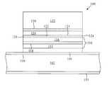
- FIG. 1shows a cross-section of a SDT device 20 having a plurality of magnetic particles 30 disposed in a tunnel barrier layer 26 .
- the device 20includes a first ferromagnetic (FM) layer 22 and second FM layer 24 separated by the tunnel barrier layer 26 .
- a pinning structure 28constrains the direction of magnetization of the second FM layer 24 .
- the magnetic moment of the first FM layer 22changes direction, as shown by arrow 27
- the magnetic moment of the second FM layer 24is pinned, as shown by arrow 29 .
- an easy axis of magnetization of the first FM layermay be substantially parallel to that of the second FM layer 24 , so that the second FM layer switches between substantially parallel and substantially antiparallel states.
- the easy axes of magnetization of the first and second FM layersare more parallel than perpendicular, switching between two states is facilitated.
- the pinning structure 28may be an antiferromagnetic (AFM) layer that adjoins the pinned layer.
- the magnetic stabilization of the pinned layermay also be accomplished with a synthetic AFM structure involving a pair of FM layers exchange coupled across a thin precious metal layer.
- ruthenium (Ru)can be used in a sandwich of FM/Ru/FM in which the Ru layer has a thickness less than 10 ⁇ .
- the magnetization direction of the pinned FM layermay be set upon deposition and annealing in a magnetic field.
- Either or both of the first and second FM layerscan be made primarily or entirely of metals such as iron (Fe), cobalt (Co), nickel (Ni) or alloys of such metals.
- Either or both of the first and second FM layersmay also be made of half-metallic magnets such as CrO 2 , Fe 3 O 4 , PtMnSb, NiMnSbCo 2 MnSi or Sr 2 FeMoO 6 .
- the tunnel barrier layer 26can be made primarily of dielectric materials such as Al 2 O 3 , AlN, SiO 2 , Si 3 N 4 , TaO, TaO 2 , Ta 2 O 5 , HfO 2 .
- a preferred tunnel barrier material in one embodimentis Al 2 O 3 .
- the magnetic particles 30can include Co, Ni or Fe atoms or molecules, or compound molecules such as CoFe, NiFe, CoNi or NiFeCo, for example. The magnetic moment of the particles is not fixed.
- a related disclosure of magnetic particles contained in a tunnel barrier layercan be found in the U.S. Patent Application entitled “Spin Dependent Tunnel Barriers Formed With A Magnetic Alloy,” invented by the same inventors and filed on the same day as the present application, and incorporated by reference herein.
- the thickness of the tunnel barrier layer 26can vary significantly for different embodiments, and for one embodiment the thickness is in a range between about 4 ⁇ and about 15 ⁇ .
- the tunnel barrier layer 26may itself be composed of plural dielectric layers with the magnetic particles disposed in at least one of the dielectric layers. Although the particles in that embodiment do not form a continuous layer that separates the dielectric layers, the average thickness of the layer of magnetic particles may be in a range between about 0.1 ⁇ and about 3 ⁇ . Individual magnetic particles in one embodiment may range between single atoms and molecules containing up to about sixteen ferromagnetic atoms. Care must be taken during fabrication to avoid having the magnetic particles act as conductors between the first and second FM layers 22 and 24 , despite an overall tunnel barrier thickness that may be as little as several atomic layers.
- FIG. 2shows a cross-section of a SDT device 60 having a plurality of magnetic particles 70 dispersed in a tunnel barrier layer 66 .
- the device 60includes a first ferromagnetic (FM) layer 62 and second FM layer 64 separated by the tunnel barrier layer 66 .
- a pinning structure 68constrains the direction of magnetization of the second FM layer 64 .
- the magnetic moment of the first FM layer 62changes direction, as shown by arrow 67
- the magnetic moment of the second FM layer 64is pinned, as shown by cross marks, indicating a moment directed away from the viewer.
- an easy axis of magnetization of the first FM layermay be substantially perpendicular to that of the second FM layer 64 , so that the second FM layer switches between low resistance and high resistance states.
- the easy axes of magnetization of the first and second FM layersare more perpendicular than parallel, a linear change in resistance is facilitated.
- FIG. 3shows a cross-section of a portion of a SDT sensor 100 in accordance with one embodiment of the invention, such as may be employed in an information storage and retrieval device.
- Formation of SDT sensor 100may occur on a wafer substrate such as AlTiC, SiC or Si, not shown, upon which a seed layer 101 of Ta has been deposited.
- a first or bottom lead 102 of electrically conductive materialsuch as Cu or Au has been formed, and capped with another Ta seed layer 104 .
- An electrically conductive layer 106 of AFM materialwas then formed on the seed layer 104 .
- the AFM materialmay, for example, include IrMn, FeMn, NiMn, PdPtMn, NiFeCr/PtMn or NiFe/PtMn.
- a magnetically pinned structure 110can then be formed of a sandwich of FM layers 112 and 116 that surround a very thin coupling layer 114 of Ru or similar elements.
- the FM layers 112 and 116which may for example be formed of CoFe, are magnetically coupled with moments directed in opposite directions about coupling layer 114 , with the moment of FM layer 112 additionally pinned by AFM layer 106 .
- a single pinned layermay be alternatively employed instead of the three layer magnetically pinned structure 110 .
- a first SDT film 120that may be between a single atomic layer and several or more nanometers in thickness, depending upon the desired application, is then deposited on the FM layer 116 .
- the first SDT film 120may be formed by depositing an initial layer, such as Al, Si, Mg, Ta or Hf on the FM layer 116 , and then oxidizing or nitridizing the initial layer.
- Magnetic particles 122are then deposited on and in some cases in the first SDT film 120 , by sputtering or ion beam depoition.
- the magnetic particles 122may range in size between individual atoms and clusters of atoms having a diameter of about 10 angstroms.
- a second SDT film 124that may be between a single atomic layer and several or more nanometers in thickness, depending upon the desired application, is then deposited on the magnetic particles 122 and the first SDT film 120 .
- the second SDT film 124may be formed by depositing an initial layer, such as Al, Si, Mg, Ta or Hf, and then oxidizing or nitridizing the initial layer.
- first SDT film 120 , magnetic particles 122 and second SDT film 124form a tunnel barrier layer 121 between pinned FM layer 116 and a free FM layer 126 .
- the thickness of tunnel barrier layer 121 for a SDT head implementationmay be between 5 ⁇ and 5 nm, the additional thickness made possible by the increased magnetoresistive effect of the novel tunnel barrier layer 121 .
- the layers 120 and 124may be oxidized or nitridized by the same or different processes, as desired for a particular application. Depending upon the process and materials employed, layers 120 and 124 may be distinct or may be merged into the single layer 121 .
- the atomic concentration of magnetic particles in a tunnel barrier layer such as layer 121may range between less than one percent and about ten percent.
- the amount of dopantscan be measured by various means, such as x-ray photoelectron spectroscopy (XPS), auger electron spectroscopy (AES), transmission electron microscopy (TEM), electron energy loss spectroscopy (EELS), parallel electron energy loss spectroscopy (PEELS), secondary ion mass spectroscopy (SIMS) or x-ray fluorescence (XRF).
- XPSx-ray photoelectron spectroscopy
- AESauger electron spectroscopy
- TEMtransmission electron microscopy
- EELSelectron energy loss spectroscopy
- PEELSparallel electron energy loss spectroscopy
- SIMSsecondary ion mass spectroscopy
- XRFx-ray fluorescence
- a free FM layer 126is formed of materials such as CoFe, NiFe, CoNiFe, or multilayers of these materials.
- a capping layer 130 of Ta, Ru, Cr or NiFeCrmay be used to prevent the oxidation of the free layer 126 .
- Edges of the SDT deviceare then defined, for example by ion beam milling into a desirable structure, and a top lead 133 is formed, e.g., of Au or Cu.
- a hard bias materialmay be formed adjacent to edges of the free layer 126 to reduce Barkhausen noise.
- a similar techniquecan be applied to form a top SDT structure, i.e., by creating a pinned layer or layers after a SDT barrier, which is formed atop a free layer.
- Other variations of the sensor stack structureare also possible that include plural magnetic particles in a tunnel barrier region.
- some portions of a pinned or free layermay be intentionally oxidized or nitridized to form a nanooxide or nanonitride that can enhance the sensitivity.
- FIG. 4shows some hysteresis plots of the magnetorestistance ( ⁇ R/R) of SDT devices having different amounts of magnetic particles contained in an alumina tunnel barrier layer such as layer 121 of FIG. 3 .
- curve 202is a plot of ( ⁇ R/R) versus applied field H for a SDT device having no magnetic particles in the barrier layer.
- a maximum ( ⁇ R/R) for this devicecan be seen to be about 31%.
- Curve 204is a plot of ( ⁇ R/R) versus applied field H for a SDT device having CoFe magnetic particles contained in a layer averaging 0.3 ⁇ in thickness within the alumina barrier layer.
- Curve 206is a plot of ( ⁇ R/R) versus applied field H for a SDT device having CoFe magnetic particles contained in a layer averaging 0.5 ⁇ in thickness within the barrier layer. A maximum ( ⁇ R/R) of about 35% for this device is significantly higher than that of the SDT device having no magnetic particles.
- FIG. 5is a plot of ( ⁇ R/R) versus a resistance-area product (RA) of SDT devices having different amounts of magnetic particles contained in an alumina tunnel barrier layer such as layer 121 of FIG. 3 .
- the diamond-shaped data points 250indicate ⁇ R/R and RA values for SDT devices having no magnetic particles in an alumina tunnel barrier layer such as layer 121 of FIG. 3 .
- the triangle-shaped data points 252indicate ⁇ R/R and RA values for SDT devices having CoFe magnetic particles contained in a layer averaging 0.3 ⁇ in thickness within the alumina barrier layer. Both the ⁇ R/R and RA values show significant improvement over the values of the undoped barrier layer.
- the circle-shaped data points 255indicate ⁇ R/R and RA values for SDT devices having CoFe magnetic particles contained in a layer averaging 0.5 ⁇ in thickness within the alumina barrier layer. Even higher ⁇ R/R and RA values are evident for this group. Magnetic particles may also be made to diffuse through a dielectric tunnel barrier layer so that, for example, they can be found at various thicknesses of the layer.
- FIG. 6shows one embodiment using the SDT devices as part of a solid-state memory such as an MRAM device 300 .
- four memory bits or cells 303 , 305 , 307 and 309are shown as stacks of layers between conductive lines arranged to write and read data to and from each cell.
- Lines 311 and 313which may be called bit lines, are used for both reading and writing and are in electrical as well as magnetic communication with the cells.
- Lines 315 and 317which may be called digit lines, are used only for writing, and are in magnetic communication with but electrically isolated from the cells.
- Word lines 321 and 323are in electrical communication with the cells via transistors, and are used only for reading.
- Each of the cells 303 , 305 , 307 and 309includes a pinned FM layer, a free FM layer and a tunnel barrier layer containing magnetic particles. Focusing on cell 305 provides an example for the operation of various cells.
- Cell 305has a pinned structure or layer 330 , a free layer 333 and a tunnel barrier layer 335 containing magnetic particles.
- a transistor 331 controlled by word line 323is coupled to a conductive lead 337 adjoining the pinned structure 330 .
- the conductive lead 337is electrically isolated from digit line 317 by insulation layer 339 .
- Pinned layer 330has a magnetic moment indicated by arrow 340
- free layer 333has a magnetic moment indicated by arrow 343
- a magnetic stateis written to cell 305 by flowing current through lines 313 and 317 in an amount sufficient to switch the magnetic moment of the free layer 333 .
- Current in line 313creates a magnetic field along a hard axis of free layer 333
- current in line 317creates a magnetic field along an easy axis of free layer 333 , the combined fields being sufficient to switch the magnetic moment of the cell, whereas either field alone is insufficient to switch the cell.
- Arrow 343is antiparallel to arrow 340 , indicating that free layer 333 has a magnetic moment antiparallel to that of pinned layer 330 .
- Turning on transistor 331 to sense the state of cell 305would result in a high voltage state (when a constant current is applied) through the transistor, which may indicate for instance that a value of zero has been stored in cell 305 .
- Cell 303has a free layer with a magnetic moment parallel to that of its pinned layer, as indicated by arrows 350 and 355 .
- Turning on transistor 351 to sense the state of cell 305would result in a low voltage state (when a constant current is applied) through the transistor, which may indicate for instance that a value of one has been stored in cell 305 .
- FIG. 7shows one embodiment using an SDT device as part of an information storage system such as a hard disk drive 400 .
- a rigid disk 402spins rapidly in a direction shown by arrow 408 relative to a head 404 containing a transducer for reading and writing magnetic patterns on a media layer 406 of the disk.
- a hard coating layer 410forms a surface of the disk 402 protecting the media layer 406 from the head 404
- a similar hard coating 412forms a surface of the head 404 to protect the transducer from the disk, while another hard coating 411 forms a trailing end of the head.
- the diskincludes a substrate 414 upon which the media layer 406 may be formed, and the disk may include additional layers, not shown.
- the headalso includes a substrate 420 upon which the transducer has been formed, and may include additional layers, not shown.
- a first shield 422has been formed over the substrate, the shield including ferromagnetic material for shielding a SDT sensor 424 from magnetic signals that are not directly opposite the sensor 424 in the media layer 406 , as well as conductive material for providing electrical current to the sensor 424 .
- a second shield 426is separated from the first shield 422 by a dielectric layer 428 , the shields connected by the sensor 424 .
- the second shield 426also includes ferromagnetic material for shielding the sensor 424 from magnetic signals that are not directly opposite the sensor 424 in the media layer 406 , as well as conductive material for providing electrical current to the sensor 424 . As the media layer 406 travels past the sensor 424 in the direction of arrow 408 , the sensor reads magnetic signals from the media layer.
- First and second ferromagnetic yoke layer 430 and 433are magnetically coupled together in a loop that is inductively driven by current in coil winding sections 435 .
- the magnetic loopis broken by a nonferromagnetic gap 438 , so that some magnetic flux propagating around the loop is diverted to the media layer 406 of the disk 402 , writing a magnetic signal to the media layer.
- This magnetic signalcan later be read by the MR sensor, which may have an increased resolution due to subnanometer magnetic particles contained in a tunnel barrier layer.
Landscapes
- Engineering & Computer Science (AREA)
- Chemical & Material Sciences (AREA)
- Crystallography & Structural Chemistry (AREA)
- Power Engineering (AREA)
- Physics & Mathematics (AREA)
- Nanotechnology (AREA)
- Computer Hardware Design (AREA)
- Condensed Matter Physics & Semiconductors (AREA)
- General Physics & Mathematics (AREA)
- Hall/Mr Elements (AREA)
Abstract
Description
Claims (30)
Priority Applications (1)
| Application Number | Priority Date | Filing Date | Title |
|---|---|---|---|
| US10/071,796US6639291B1 (en) | 2002-02-06 | 2002-02-06 | Spin dependent tunneling barriers doped with magnetic particles |
Applications Claiming Priority (1)
| Application Number | Priority Date | Filing Date | Title |
|---|---|---|---|
| US10/071,796US6639291B1 (en) | 2002-02-06 | 2002-02-06 | Spin dependent tunneling barriers doped with magnetic particles |
Publications (1)
| Publication Number | Publication Date |
|---|---|
| US6639291B1true US6639291B1 (en) | 2003-10-28 |
Family
ID=29248118
Family Applications (1)
| Application Number | Title | Priority Date | Filing Date |
|---|---|---|---|
| US10/071,796Expired - LifetimeUS6639291B1 (en) | 2002-02-06 | 2002-02-06 | Spin dependent tunneling barriers doped with magnetic particles |
Country Status (1)
| Country | Link |
|---|---|
| US (1) | US6639291B1 (en) |
Cited By (143)
| Publication number | Priority date | Publication date | Assignee | Title |
|---|---|---|---|---|
| US20050141148A1 (en)* | 2003-12-02 | 2005-06-30 | Kabushiki Kaisha Toshiba | Magnetic memory |
| US20050179483A1 (en)* | 2003-11-18 | 2005-08-18 | Hutchens Chriswell G. | High-voltage transistors on insulator substrates |
| EP1566651A1 (en)* | 2004-02-20 | 2005-08-24 | TDK Corporation | Magnetic sensing device, method of forming the same, magnetic sensor and ammeter |
| US20050213376A1 (en)* | 2004-02-04 | 2005-09-29 | Sony Corporation | Magnetic memory device and its driving method and magnetic memory |
| US6958927B1 (en)* | 2002-10-09 | 2005-10-25 | Grandis Inc. | Magnetic element utilizing spin-transfer and half-metals and an MRAM device using the magnetic element |
| US20050237309A1 (en)* | 2004-04-26 | 2005-10-27 | Manish Sharma | Input device including a layer of particles |
| US20050276099A1 (en)* | 2004-06-15 | 2005-12-15 | Headway Technologies, Inc. | Novel capping structure for enhancing dR/R of the MTJ device |
| US20060233002A1 (en)* | 2005-03-30 | 2006-10-19 | Taiwan Semiconductor Manufacturing Co., Ltd. | Memory cell structure |
| US20060244021A1 (en)* | 2005-04-29 | 2006-11-02 | Ulrich Klostermann | Adiabatic rotational switching memory element including a ferromagnetic decoupling layer |
| US20090243007A1 (en)* | 2005-09-20 | 2009-10-01 | Freescale Seminconductor, Inc. | Spin-dependent tunnelling cell and method of formation thereof |
| US8766383B2 (en) | 2011-07-07 | 2014-07-01 | Samsung Electronics Co., Ltd. | Method and system for providing a magnetic junction using half metallic ferromagnets |
| US8830628B1 (en) | 2009-02-23 | 2014-09-09 | Western Digital (Fremont), Llc | Method and system for providing a perpendicular magnetic recording head |
| US8879207B1 (en) | 2011-12-20 | 2014-11-04 | Western Digital (Fremont), Llc | Method for providing a side shield for a magnetic recording transducer using an air bridge |
| US8883017B1 (en) | 2013-03-12 | 2014-11-11 | Western Digital (Fremont), Llc | Method and system for providing a read transducer having seamless interfaces |
| US8917581B1 (en) | 2013-12-18 | 2014-12-23 | Western Digital Technologies, Inc. | Self-anneal process for a near field transducer and chimney in a hard disk drive assembly |
| US8923102B1 (en) | 2013-07-16 | 2014-12-30 | Western Digital (Fremont), Llc | Optical grating coupling for interferometric waveguides in heat assisted magnetic recording heads |
| US8947985B1 (en) | 2013-07-16 | 2015-02-03 | Western Digital (Fremont), Llc | Heat assisted magnetic recording transducers having a recessed pole |
| US8953422B1 (en) | 2014-06-10 | 2015-02-10 | Western Digital (Fremont), Llc | Near field transducer using dielectric waveguide core with fine ridge feature |
| US8958272B1 (en) | 2014-06-10 | 2015-02-17 | Western Digital (Fremont), Llc | Interfering near field transducer for energy assisted magnetic recording |
| US8970988B1 (en) | 2013-12-31 | 2015-03-03 | Western Digital (Fremont), Llc | Electric gaps and method for making electric gaps for multiple sensor arrays |
| US8971160B1 (en) | 2013-12-19 | 2015-03-03 | Western Digital (Fremont), Llc | Near field transducer with high refractive index pin for heat assisted magnetic recording |
| US8976635B1 (en) | 2014-06-10 | 2015-03-10 | Western Digital (Fremont), Llc | Near field transducer driven by a transverse electric waveguide for energy assisted magnetic recording |
| US8980109B1 (en) | 2012-12-11 | 2015-03-17 | Western Digital (Fremont), Llc | Method for providing a magnetic recording transducer using a combined main pole and side shield CMP for a wraparound shield scheme |
| US8982508B1 (en) | 2011-10-31 | 2015-03-17 | Western Digital (Fremont), Llc | Method for providing a side shield for a magnetic recording transducer |
| US8988825B1 (en) | 2014-02-28 | 2015-03-24 | Western Digital (Fremont, LLC | Method for fabricating a magnetic writer having half-side shields |
| US8984740B1 (en) | 2012-11-30 | 2015-03-24 | Western Digital (Fremont), Llc | Process for providing a magnetic recording transducer having a smooth magnetic seed layer |
| US8988812B1 (en) | 2013-11-27 | 2015-03-24 | Western Digital (Fremont), Llc | Multi-sensor array configuration for a two-dimensional magnetic recording (TDMR) operation |
| US8993217B1 (en) | 2013-04-04 | 2015-03-31 | Western Digital (Fremont), Llc | Double exposure technique for high resolution disk imaging |
| US8995087B1 (en) | 2006-11-29 | 2015-03-31 | Western Digital (Fremont), Llc | Perpendicular magnetic recording write head having a wrap around shield |
| US9001467B1 (en) | 2014-03-05 | 2015-04-07 | Western Digital (Fremont), Llc | Method for fabricating side shields in a magnetic writer |
| US9001628B1 (en) | 2013-12-16 | 2015-04-07 | Western Digital (Fremont), Llc | Assistant waveguides for evaluating main waveguide coupling efficiency and diode laser alignment tolerances for hard disk |
| US8997832B1 (en) | 2010-11-23 | 2015-04-07 | Western Digital (Fremont), Llc | Method of fabricating micrometer scale components |
| US9007719B1 (en) | 2013-10-23 | 2015-04-14 | Western Digital (Fremont), Llc | Systems and methods for using double mask techniques to achieve very small features |
| US9007879B1 (en) | 2014-06-10 | 2015-04-14 | Western Digital (Fremont), Llc | Interfering near field transducer having a wide metal bar feature for energy assisted magnetic recording |
| US9007725B1 (en) | 2014-10-07 | 2015-04-14 | Western Digital (Fremont), Llc | Sensor with positive coupling between dual ferromagnetic free layer laminates |
| US9013836B1 (en) | 2013-04-02 | 2015-04-21 | Western Digital (Fremont), Llc | Method and system for providing an antiferromagnetically coupled return pole |
| US9042057B1 (en) | 2013-01-09 | 2015-05-26 | Western Digital (Fremont), Llc | Methods for providing magnetic storage elements with high magneto-resistance using Heusler alloys |
| US9042052B1 (en) | 2014-06-23 | 2015-05-26 | Western Digital (Fremont), Llc | Magnetic writer having a partially shunted coil |
| US9042058B1 (en) | 2013-10-17 | 2015-05-26 | Western Digital Technologies, Inc. | Shield designed for middle shields in a multiple sensor array |
| US9042051B2 (en) | 2013-08-15 | 2015-05-26 | Western Digital (Fremont), Llc | Gradient write gap for perpendicular magnetic recording writer |
| US9042208B1 (en) | 2013-03-11 | 2015-05-26 | Western Digital Technologies, Inc. | Disk drive measuring fly height by applying a bias voltage to an electrically insulated write component of a head |
| US9053735B1 (en) | 2014-06-20 | 2015-06-09 | Western Digital (Fremont), Llc | Method for fabricating a magnetic writer using a full-film metal planarization |
| US9065043B1 (en) | 2012-06-29 | 2015-06-23 | Western Digital (Fremont), Llc | Tunnel magnetoresistance read head with narrow shield-to-shield spacing |
| US9064507B1 (en) | 2009-07-31 | 2015-06-23 | Western Digital (Fremont), Llc | Magnetic etch-stop layer for magnetoresistive read heads |
| US9064528B1 (en) | 2013-05-17 | 2015-06-23 | Western Digital Technologies, Inc. | Interferometric waveguide usable in shingled heat assisted magnetic recording in the absence of a near-field transducer |
| US9064527B1 (en) | 2013-04-12 | 2015-06-23 | Western Digital (Fremont), Llc | High order tapered waveguide for use in a heat assisted magnetic recording head |
| US9070381B1 (en) | 2013-04-12 | 2015-06-30 | Western Digital (Fremont), Llc | Magnetic recording read transducer having a laminated free layer |
| US9082423B1 (en) | 2013-12-18 | 2015-07-14 | Western Digital (Fremont), Llc | Magnetic recording write transducer having an improved trailing surface profile |
| US9087534B1 (en) | 2011-12-20 | 2015-07-21 | Western Digital (Fremont), Llc | Method and system for providing a read transducer having soft and hard magnetic bias structures |
| US9087527B1 (en) | 2014-10-28 | 2015-07-21 | Western Digital (Fremont), Llc | Apparatus and method for middle shield connection in magnetic recording transducers |
| US9093639B2 (en) | 2012-02-21 | 2015-07-28 | Western Digital (Fremont), Llc | Methods for manufacturing a magnetoresistive structure utilizing heating and cooling |
| US9104107B1 (en) | 2013-04-03 | 2015-08-11 | Western Digital (Fremont), Llc | DUV photoresist process |
| US9111558B1 (en) | 2014-03-14 | 2015-08-18 | Western Digital (Fremont), Llc | System and method of diffractive focusing of light in a waveguide |
| US9111564B1 (en) | 2013-04-02 | 2015-08-18 | Western Digital (Fremont), Llc | Magnetic recording writer having a main pole with multiple flare angles |
| US9111550B1 (en) | 2014-12-04 | 2015-08-18 | Western Digital (Fremont), Llc | Write transducer having a magnetic buffer layer spaced between a side shield and a write pole by non-magnetic layers |
| US9123358B1 (en) | 2012-06-11 | 2015-09-01 | Western Digital (Fremont), Llc | Conformal high moment side shield seed layer for perpendicular magnetic recording writer |
| US9123374B1 (en) | 2015-02-12 | 2015-09-01 | Western Digital (Fremont), Llc | Heat assisted magnetic recording writer having an integrated polarization rotation plate |
| US9123362B1 (en) | 2011-03-22 | 2015-09-01 | Western Digital (Fremont), Llc | Methods for assembling an electrically assisted magnetic recording (EAMR) head |
| US9123359B1 (en) | 2010-12-22 | 2015-09-01 | Western Digital (Fremont), Llc | Magnetic recording transducer with sputtered antiferromagnetic coupling trilayer between plated ferromagnetic shields and method of fabrication |
| US9135930B1 (en) | 2014-03-06 | 2015-09-15 | Western Digital (Fremont), Llc | Method for fabricating a magnetic write pole using vacuum deposition |
| US9135937B1 (en) | 2014-05-09 | 2015-09-15 | Western Digital (Fremont), Llc | Current modulation on laser diode for energy assisted magnetic recording transducer |
| US9142233B1 (en) | 2014-02-28 | 2015-09-22 | Western Digital (Fremont), Llc | Heat assisted magnetic recording writer having a recessed pole |
| US9147408B1 (en) | 2013-12-19 | 2015-09-29 | Western Digital (Fremont), Llc | Heated AFM layer deposition and cooling process for TMR magnetic recording sensor with high pinning field |
| US9147404B1 (en) | 2015-03-31 | 2015-09-29 | Western Digital (Fremont), Llc | Method and system for providing a read transducer having a dual free layer |
| US9153255B1 (en) | 2014-03-05 | 2015-10-06 | Western Digital (Fremont), Llc | Method for fabricating a magnetic writer having an asymmetric gap and shields |
| US9183854B2 (en) | 2014-02-24 | 2015-11-10 | Western Digital (Fremont), Llc | Method to make interferometric taper waveguide for HAMR light delivery |
| US9190085B1 (en) | 2014-03-12 | 2015-11-17 | Western Digital (Fremont), Llc | Waveguide with reflective grating for localized energy intensity |
| US9190079B1 (en) | 2014-09-22 | 2015-11-17 | Western Digital (Fremont), Llc | Magnetic write pole having engineered radius of curvature and chisel angle profiles |
| US9194692B1 (en) | 2013-12-06 | 2015-11-24 | Western Digital (Fremont), Llc | Systems and methods for using white light interferometry to measure undercut of a bi-layer structure |
| US9202493B1 (en) | 2014-02-28 | 2015-12-01 | Western Digital (Fremont), Llc | Method of making an ultra-sharp tip mode converter for a HAMR head |
| US9202480B2 (en) | 2009-10-14 | 2015-12-01 | Western Digital (Fremont), LLC. | Double patterning hard mask for damascene perpendicular magnetic recording (PMR) writer |
| US9214165B1 (en) | 2014-12-18 | 2015-12-15 | Western Digital (Fremont), Llc | Magnetic writer having a gradient in saturation magnetization of the shields |
| US9214172B2 (en) | 2013-10-23 | 2015-12-15 | Western Digital (Fremont), Llc | Method of manufacturing a magnetic read head |
| US9214169B1 (en) | 2014-06-20 | 2015-12-15 | Western Digital (Fremont), Llc | Magnetic recording read transducer having a laminated free layer |
| US9213322B1 (en) | 2012-08-16 | 2015-12-15 | Western Digital (Fremont), Llc | Methods for providing run to run process control using a dynamic tuner |
| US9230565B1 (en) | 2014-06-24 | 2016-01-05 | Western Digital (Fremont), Llc | Magnetic shield for magnetic recording head |
| US9236560B1 (en) | 2014-12-08 | 2016-01-12 | Western Digital (Fremont), Llc | Spin transfer torque tunneling magnetoresistive device having a laminated free layer with perpendicular magnetic anisotropy |
| US9245562B1 (en) | 2015-03-30 | 2016-01-26 | Western Digital (Fremont), Llc | Magnetic recording writer with a composite main pole |
| US9245545B1 (en) | 2013-04-12 | 2016-01-26 | Wester Digital (Fremont), Llc | Short yoke length coils for magnetic heads in disk drives |
| US9245543B1 (en) | 2010-06-25 | 2016-01-26 | Western Digital (Fremont), Llc | Method for providing an energy assisted magnetic recording head having a laser integrally mounted to the slider |
| US9251813B1 (en) | 2009-04-19 | 2016-02-02 | Western Digital (Fremont), Llc | Method of making a magnetic recording head |
| US9263067B1 (en) | 2013-05-29 | 2016-02-16 | Western Digital (Fremont), Llc | Process for making PMR writer with constant side wall angle |
| US9263071B1 (en) | 2015-03-31 | 2016-02-16 | Western Digital (Fremont), Llc | Flat NFT for heat assisted magnetic recording |
| US9269382B1 (en) | 2012-06-29 | 2016-02-23 | Western Digital (Fremont), Llc | Method and system for providing a read transducer having improved pinning of the pinned layer at higher recording densities |
| US9275657B1 (en) | 2013-08-14 | 2016-03-01 | Western Digital (Fremont), Llc | Process for making PMR writer with non-conformal side gaps |
| US9280990B1 (en) | 2013-12-11 | 2016-03-08 | Western Digital (Fremont), Llc | Method for fabricating a magnetic writer using multiple etches |
| US9287494B1 (en) | 2013-06-28 | 2016-03-15 | Western Digital (Fremont), Llc | Magnetic tunnel junction (MTJ) with a magnesium oxide tunnel barrier |
| US9286919B1 (en) | 2014-12-17 | 2016-03-15 | Western Digital (Fremont), Llc | Magnetic writer having a dual side gap |
| US9305583B1 (en) | 2014-02-18 | 2016-04-05 | Western Digital (Fremont), Llc | Method for fabricating a magnetic writer using multiple etches of damascene materials |
| US9312064B1 (en) | 2015-03-02 | 2016-04-12 | Western Digital (Fremont), Llc | Method to fabricate a magnetic head including ion milling of read gap using dual layer hard mask |
| US9318130B1 (en) | 2013-07-02 | 2016-04-19 | Western Digital (Fremont), Llc | Method to fabricate tunneling magnetic recording heads with extended pinned layer |
| US9336814B1 (en) | 2013-03-12 | 2016-05-10 | Western Digital (Fremont), Llc | Inverse tapered waveguide for use in a heat assisted magnetic recording head |
| US9343098B1 (en) | 2013-08-23 | 2016-05-17 | Western Digital (Fremont), Llc | Method for providing a heat assisted magnetic recording transducer having protective pads |
| US9343086B1 (en) | 2013-09-11 | 2016-05-17 | Western Digital (Fremont), Llc | Magnetic recording write transducer having an improved sidewall angle profile |
| US9343087B1 (en) | 2014-12-21 | 2016-05-17 | Western Digital (Fremont), Llc | Method for fabricating a magnetic writer having half shields |
| US9349394B1 (en) | 2013-10-18 | 2016-05-24 | Western Digital (Fremont), Llc | Method for fabricating a magnetic writer having a gradient side gap |
| US9349392B1 (en) | 2012-05-24 | 2016-05-24 | Western Digital (Fremont), Llc | Methods for improving adhesion on dielectric substrates |
| US9361914B1 (en) | 2014-06-18 | 2016-06-07 | Western Digital (Fremont), Llc | Magnetic sensor with thin capping layer |
| US9361913B1 (en) | 2013-06-03 | 2016-06-07 | Western Digital (Fremont), Llc | Recording read heads with a multi-layer AFM layer methods and apparatuses |
| US9368134B1 (en) | 2010-12-16 | 2016-06-14 | Western Digital (Fremont), Llc | Method and system for providing an antiferromagnetically coupled writer |
| US9384765B1 (en) | 2015-09-24 | 2016-07-05 | Western Digital (Fremont), Llc | Method and system for providing a HAMR writer having improved optical efficiency |
| US9384763B1 (en) | 2015-03-26 | 2016-07-05 | Western Digital (Fremont), Llc | Dual free layer magnetic reader having a rear bias structure including a soft bias layer |
| US9396743B1 (en) | 2014-02-28 | 2016-07-19 | Western Digital (Fremont), Llc | Systems and methods for controlling soft bias thickness for tunnel magnetoresistance readers |
| US9396742B1 (en) | 2012-11-30 | 2016-07-19 | Western Digital (Fremont), Llc | Magnetoresistive sensor for a magnetic storage system read head, and fabrication method thereof |
| US9406331B1 (en) | 2013-06-17 | 2016-08-02 | Western Digital (Fremont), Llc | Method for making ultra-narrow read sensor and read transducer device resulting therefrom |
| US9424866B1 (en) | 2015-09-24 | 2016-08-23 | Western Digital (Fremont), Llc | Heat assisted magnetic recording write apparatus having a dielectric gap |
| US9431047B1 (en) | 2013-05-01 | 2016-08-30 | Western Digital (Fremont), Llc | Method for providing an improved AFM reader shield |
| US9431038B1 (en) | 2015-06-29 | 2016-08-30 | Western Digital (Fremont), Llc | Method for fabricating a magnetic write pole having an improved sidewall angle profile |
| US9431031B1 (en) | 2015-03-24 | 2016-08-30 | Western Digital (Fremont), Llc | System and method for magnetic transducers having multiple sensors and AFC shields |
| US9431039B1 (en) | 2013-05-21 | 2016-08-30 | Western Digital (Fremont), Llc | Multiple sensor array usable in two-dimensional magnetic recording |
| US9431032B1 (en) | 2013-08-14 | 2016-08-30 | Western Digital (Fremont), Llc | Electrical connection arrangement for a multiple sensor array usable in two-dimensional magnetic recording |
| US9437251B1 (en) | 2014-12-22 | 2016-09-06 | Western Digital (Fremont), Llc | Apparatus and method having TDMR reader to reader shunts |
| US9443541B1 (en) | 2015-03-24 | 2016-09-13 | Western Digital (Fremont), Llc | Magnetic writer having a gradient in saturation magnetization of the shields and return pole |
| US9441938B1 (en) | 2013-10-08 | 2016-09-13 | Western Digital (Fremont), Llc | Test structures for measuring near field transducer disc length |
| US9449621B1 (en) | 2015-03-26 | 2016-09-20 | Western Digital (Fremont), Llc | Dual free layer magnetic reader having a rear bias structure having a high aspect ratio |
| US9449625B1 (en) | 2014-12-24 | 2016-09-20 | Western Digital (Fremont), Llc | Heat assisted magnetic recording head having a plurality of diffusion barrier layers |
| US9472216B1 (en) | 2015-09-23 | 2016-10-18 | Western Digital (Fremont), Llc | Differential dual free layer magnetic reader |
| US9484051B1 (en) | 2015-11-09 | 2016-11-01 | The Provost, Fellows, Foundation Scholars and the other members of Board, of the College of the Holy and Undivided Trinity of Queen Elizabeth near Dublin | Method and system for reducing undesirable reflections in a HAMR write apparatus |
| US9508372B1 (en) | 2015-06-03 | 2016-11-29 | Western Digital (Fremont), Llc | Shingle magnetic writer having a low sidewall angle pole |
| US9508365B1 (en) | 2015-06-24 | 2016-11-29 | Western Digital (Fremont), LLC. | Magnetic reader having a crystal decoupling structure |
| US9508363B1 (en) | 2014-06-17 | 2016-11-29 | Western Digital (Fremont), Llc | Method for fabricating a magnetic write pole having a leading edge bevel |
| US9530443B1 (en) | 2015-06-25 | 2016-12-27 | Western Digital (Fremont), Llc | Method for fabricating a magnetic recording device having a high aspect ratio structure |
| US9564150B1 (en) | 2015-11-24 | 2017-02-07 | Western Digital (Fremont), Llc | Magnetic read apparatus having an improved read sensor isolation circuit |
| CN106449738A (en)* | 2016-07-21 | 2017-02-22 | 北京航空航天大学 | A Coaxial Spin Injection Device |
| US9595273B1 (en) | 2015-09-30 | 2017-03-14 | Western Digital (Fremont), Llc | Shingle magnetic writer having nonconformal shields |
| US9646639B2 (en) | 2015-06-26 | 2017-05-09 | Western Digital (Fremont), Llc | Heat assisted magnetic recording writer having integrated polarization rotation waveguides |
| US9666214B1 (en) | 2015-09-23 | 2017-05-30 | Western Digital (Fremont), Llc | Free layer magnetic reader that may have a reduced shield-to-shield spacing |
| US9721595B1 (en) | 2014-12-04 | 2017-08-01 | Western Digital (Fremont), Llc | Method for providing a storage device |
| US9740805B1 (en) | 2015-12-01 | 2017-08-22 | Western Digital (Fremont), Llc | Method and system for detecting hotspots for photolithographically-defined devices |
| US9741366B1 (en) | 2014-12-18 | 2017-08-22 | Western Digital (Fremont), Llc | Method for fabricating a magnetic writer having a gradient in saturation magnetization of the shields |
| US9754611B1 (en) | 2015-11-30 | 2017-09-05 | Western Digital (Fremont), Llc | Magnetic recording write apparatus having a stepped conformal trailing shield |
| US9767831B1 (en) | 2015-12-01 | 2017-09-19 | Western Digital (Fremont), Llc | Magnetic writer having convex trailing surface pole and conformal write gap |
| US9786301B1 (en) | 2014-12-02 | 2017-10-10 | Western Digital (Fremont), Llc | Apparatuses and methods for providing thin shields in a multiple sensor array |
| US9799351B1 (en) | 2015-11-30 | 2017-10-24 | Western Digital (Fremont), Llc | Short yoke length writer having assist coils |
| US9812155B1 (en) | 2015-11-23 | 2017-11-07 | Western Digital (Fremont), Llc | Method and system for fabricating high junction angle read sensors |
| US9842615B1 (en) | 2015-06-26 | 2017-12-12 | Western Digital (Fremont), Llc | Magnetic reader having a nonmagnetic insertion layer for the pinning layer |
| US9858951B1 (en) | 2015-12-01 | 2018-01-02 | Western Digital (Fremont), Llc | Method for providing a multilayer AFM layer in a read sensor |
| US9881638B1 (en) | 2014-12-17 | 2018-01-30 | Western Digital (Fremont), Llc | Method for providing a near-field transducer (NFT) for a heat assisted magnetic recording (HAMR) device |
| US9934811B1 (en) | 2014-03-07 | 2018-04-03 | Western Digital (Fremont), Llc | Methods for controlling stray fields of magnetic features using magneto-elastic anisotropy |
| US9953670B1 (en) | 2015-11-10 | 2018-04-24 | Western Digital (Fremont), Llc | Method and system for providing a HAMR writer including a multi-mode interference device |
| US10037770B1 (en) | 2015-11-12 | 2018-07-31 | Western Digital (Fremont), Llc | Method for providing a magnetic recording write apparatus having a seamless pole |
| US10074387B1 (en) | 2014-12-21 | 2018-09-11 | Western Digital (Fremont), Llc | Method and system for providing a read transducer having symmetric antiferromagnetically coupled shields |
| US20200194311A1 (en)* | 2017-11-08 | 2020-06-18 | Tdk Corporation | Tunnel magnetoresistive effect element, magnetic memory, and built-in memory |
Citations (1)
| Publication number | Priority date | Publication date | Assignee | Title |
|---|---|---|---|---|
| US20030035253A1 (en)* | 2001-08-17 | 2003-02-20 | Tsann Lin | Magnetoresistance sensors with Pt-Mn transverse and longitudinal pinning layers, and their fabrication method |
- 2002
- 2002-02-06USUS10/071,796patent/US6639291B1/ennot_activeExpired - Lifetime
Patent Citations (1)
| Publication number | Priority date | Publication date | Assignee | Title |
|---|---|---|---|---|
| US20030035253A1 (en)* | 2001-08-17 | 2003-02-20 | Tsann Lin | Magnetoresistance sensors with Pt-Mn transverse and longitudinal pinning layers, and their fabrication method |
Cited By (179)
| Publication number | Priority date | Publication date | Assignee | Title |
|---|---|---|---|---|
| US7227773B1 (en) | 2002-10-09 | 2007-06-05 | Grandis, Inc. | Magnetic element utilizing spin-transfer and half-metals and an MRAM device using the magnetic element |
| US6958927B1 (en)* | 2002-10-09 | 2005-10-25 | Grandis Inc. | Magnetic element utilizing spin-transfer and half-metals and an MRAM device using the magnetic element |
| US20050195627A1 (en)* | 2003-11-18 | 2005-09-08 | Hutchens Chriswell G. | High-temperature memory systems |
| US20050179483A1 (en)* | 2003-11-18 | 2005-08-18 | Hutchens Chriswell G. | High-voltage transistors on insulator substrates |
| US7848136B2 (en) | 2003-12-02 | 2010-12-07 | Kabushiki Kaisha Toshiba | Magnetic memory |
| US20050141148A1 (en)* | 2003-12-02 | 2005-06-30 | Kabushiki Kaisha Toshiba | Magnetic memory |
| US20080204944A1 (en)* | 2003-12-02 | 2008-08-28 | Kabushiki Kaisha Toshiba | Magnetic memory |
| US20050213376A1 (en)* | 2004-02-04 | 2005-09-29 | Sony Corporation | Magnetic memory device and its driving method and magnetic memory |
| US7459737B2 (en)* | 2004-02-04 | 2008-12-02 | Sony Corporation | Low current magnetic memory |
| US20050185346A1 (en)* | 2004-02-20 | 2005-08-25 | Tdk Corporation | Magnetic sensing device, method of forming the same, magnetic sensor, and ammeter |
| US7248045B2 (en) | 2004-02-20 | 2007-07-24 | Tdk Corporation | Magnetic sensing device, method of forming the same, magnetic sensor, and ammeter |
| CN100443914C (en)* | 2004-02-20 | 2008-12-17 | Tdk株式会社 | Magnetic detection element, method of forming same, and magnetic sensor and galvanometer |
| EP1566651A1 (en)* | 2004-02-20 | 2005-08-24 | TDK Corporation | Magnetic sensing device, method of forming the same, magnetic sensor and ammeter |
| US20050237309A1 (en)* | 2004-04-26 | 2005-10-27 | Manish Sharma | Input device including a layer of particles |
| EP1607980A3 (en)* | 2004-06-15 | 2006-06-14 | Headway Technologies, Inc. | A novel capping structure for enhancing dR/R of the MTJ device |
| US7449345B2 (en) | 2004-06-15 | 2008-11-11 | Headway Technologies, Inc. | Capping structure for enhancing dR/R of the MTJ device |
| KR101142820B1 (en)* | 2004-06-15 | 2012-05-08 | 어플라이드 스핀트로닉스, 인크. | A novel capping structure for enhancing dR/R of the MTJ device |
| US20050276099A1 (en)* | 2004-06-15 | 2005-12-15 | Headway Technologies, Inc. | Novel capping structure for enhancing dR/R of the MTJ device |
| US7312506B2 (en)* | 2005-03-30 | 2007-12-25 | Taiwan Semiconductor Manufacturing Co., Ltd. | Memory cell structure |
| US20060233002A1 (en)* | 2005-03-30 | 2006-10-19 | Taiwan Semiconductor Manufacturing Co., Ltd. | Memory cell structure |
| US7205596B2 (en)* | 2005-04-29 | 2007-04-17 | Infineon Technologies, Ag | Adiabatic rotational switching memory element including a ferromagnetic decoupling layer |
| US20060244021A1 (en)* | 2005-04-29 | 2006-11-02 | Ulrich Klostermann | Adiabatic rotational switching memory element including a ferromagnetic decoupling layer |
| US20090243007A1 (en)* | 2005-09-20 | 2009-10-01 | Freescale Seminconductor, Inc. | Spin-dependent tunnelling cell and method of formation thereof |
| US7867788B2 (en)* | 2005-09-20 | 2011-01-11 | Freescale Semiconductor, Inc. | Spin-dependent tunnelling cell and method of formation thereof |
| US8995087B1 (en) | 2006-11-29 | 2015-03-31 | Western Digital (Fremont), Llc | Perpendicular magnetic recording write head having a wrap around shield |
| US8830628B1 (en) | 2009-02-23 | 2014-09-09 | Western Digital (Fremont), Llc | Method and system for providing a perpendicular magnetic recording head |
| US9251813B1 (en) | 2009-04-19 | 2016-02-02 | Western Digital (Fremont), Llc | Method of making a magnetic recording head |
| US9064507B1 (en) | 2009-07-31 | 2015-06-23 | Western Digital (Fremont), Llc | Magnetic etch-stop layer for magnetoresistive read heads |
| US9202480B2 (en) | 2009-10-14 | 2015-12-01 | Western Digital (Fremont), LLC. | Double patterning hard mask for damascene perpendicular magnetic recording (PMR) writer |
| US9245543B1 (en) | 2010-06-25 | 2016-01-26 | Western Digital (Fremont), Llc | Method for providing an energy assisted magnetic recording head having a laser integrally mounted to the slider |
| US8997832B1 (en) | 2010-11-23 | 2015-04-07 | Western Digital (Fremont), Llc | Method of fabricating micrometer scale components |
| US9159345B1 (en) | 2010-11-23 | 2015-10-13 | Western Digital (Fremont), Llc | Micrometer scale components |
| US9672847B2 (en) | 2010-11-23 | 2017-06-06 | Western Digital (Fremont), Llc | Micrometer scale components |
| US9368134B1 (en) | 2010-12-16 | 2016-06-14 | Western Digital (Fremont), Llc | Method and system for providing an antiferromagnetically coupled writer |
| US9123359B1 (en) | 2010-12-22 | 2015-09-01 | Western Digital (Fremont), Llc | Magnetic recording transducer with sputtered antiferromagnetic coupling trilayer between plated ferromagnetic shields and method of fabrication |
| US9123362B1 (en) | 2011-03-22 | 2015-09-01 | Western Digital (Fremont), Llc | Methods for assembling an electrically assisted magnetic recording (EAMR) head |
| US8766383B2 (en) | 2011-07-07 | 2014-07-01 | Samsung Electronics Co., Ltd. | Method and system for providing a magnetic junction using half metallic ferromagnets |
| US8982508B1 (en) | 2011-10-31 | 2015-03-17 | Western Digital (Fremont), Llc | Method for providing a side shield for a magnetic recording transducer |
| US9087534B1 (en) | 2011-12-20 | 2015-07-21 | Western Digital (Fremont), Llc | Method and system for providing a read transducer having soft and hard magnetic bias structures |
| US8879207B1 (en) | 2011-12-20 | 2014-11-04 | Western Digital (Fremont), Llc | Method for providing a side shield for a magnetic recording transducer using an air bridge |
| US9093639B2 (en) | 2012-02-21 | 2015-07-28 | Western Digital (Fremont), Llc | Methods for manufacturing a magnetoresistive structure utilizing heating and cooling |
| US9349392B1 (en) | 2012-05-24 | 2016-05-24 | Western Digital (Fremont), Llc | Methods for improving adhesion on dielectric substrates |
| US9940950B2 (en) | 2012-05-24 | 2018-04-10 | Western Digital (Fremont), Llc | Methods for improving adhesion on dielectric substrates |
| US9123358B1 (en) | 2012-06-11 | 2015-09-01 | Western Digital (Fremont), Llc | Conformal high moment side shield seed layer for perpendicular magnetic recording writer |
| US9269382B1 (en) | 2012-06-29 | 2016-02-23 | Western Digital (Fremont), Llc | Method and system for providing a read transducer having improved pinning of the pinned layer at higher recording densities |
| US9065043B1 (en) | 2012-06-29 | 2015-06-23 | Western Digital (Fremont), Llc | Tunnel magnetoresistance read head with narrow shield-to-shield spacing |
| US9412400B2 (en) | 2012-06-29 | 2016-08-09 | Western Digital (Fremont), Llc | Tunnel magnetoresistance read head with narrow shield-to-shield spacing |
| US9213322B1 (en) | 2012-08-16 | 2015-12-15 | Western Digital (Fremont), Llc | Methods for providing run to run process control using a dynamic tuner |
| US9396742B1 (en) | 2012-11-30 | 2016-07-19 | Western Digital (Fremont), Llc | Magnetoresistive sensor for a magnetic storage system read head, and fabrication method thereof |
| US8984740B1 (en) | 2012-11-30 | 2015-03-24 | Western Digital (Fremont), Llc | Process for providing a magnetic recording transducer having a smooth magnetic seed layer |
| US8980109B1 (en) | 2012-12-11 | 2015-03-17 | Western Digital (Fremont), Llc | Method for providing a magnetic recording transducer using a combined main pole and side shield CMP for a wraparound shield scheme |
| US9042057B1 (en) | 2013-01-09 | 2015-05-26 | Western Digital (Fremont), Llc | Methods for providing magnetic storage elements with high magneto-resistance using Heusler alloys |
| US9042208B1 (en) | 2013-03-11 | 2015-05-26 | Western Digital Technologies, Inc. | Disk drive measuring fly height by applying a bias voltage to an electrically insulated write component of a head |
| US8883017B1 (en) | 2013-03-12 | 2014-11-11 | Western Digital (Fremont), Llc | Method and system for providing a read transducer having seamless interfaces |
| US9336814B1 (en) | 2013-03-12 | 2016-05-10 | Western Digital (Fremont), Llc | Inverse tapered waveguide for use in a heat assisted magnetic recording head |
| US9013836B1 (en) | 2013-04-02 | 2015-04-21 | Western Digital (Fremont), Llc | Method and system for providing an antiferromagnetically coupled return pole |
| US9111564B1 (en) | 2013-04-02 | 2015-08-18 | Western Digital (Fremont), Llc | Magnetic recording writer having a main pole with multiple flare angles |
| US9104107B1 (en) | 2013-04-03 | 2015-08-11 | Western Digital (Fremont), Llc | DUV photoresist process |
| US8993217B1 (en) | 2013-04-04 | 2015-03-31 | Western Digital (Fremont), Llc | Double exposure technique for high resolution disk imaging |
| US9064527B1 (en) | 2013-04-12 | 2015-06-23 | Western Digital (Fremont), Llc | High order tapered waveguide for use in a heat assisted magnetic recording head |
| US9070381B1 (en) | 2013-04-12 | 2015-06-30 | Western Digital (Fremont), Llc | Magnetic recording read transducer having a laminated free layer |
| US9245545B1 (en) | 2013-04-12 | 2016-01-26 | Wester Digital (Fremont), Llc | Short yoke length coils for magnetic heads in disk drives |
| US9431047B1 (en) | 2013-05-01 | 2016-08-30 | Western Digital (Fremont), Llc | Method for providing an improved AFM reader shield |
| US9064528B1 (en) | 2013-05-17 | 2015-06-23 | Western Digital Technologies, Inc. | Interferometric waveguide usable in shingled heat assisted magnetic recording in the absence of a near-field transducer |
| US9431039B1 (en) | 2013-05-21 | 2016-08-30 | Western Digital (Fremont), Llc | Multiple sensor array usable in two-dimensional magnetic recording |
| US9263067B1 (en) | 2013-05-29 | 2016-02-16 | Western Digital (Fremont), Llc | Process for making PMR writer with constant side wall angle |
| US9361913B1 (en) | 2013-06-03 | 2016-06-07 | Western Digital (Fremont), Llc | Recording read heads with a multi-layer AFM layer methods and apparatuses |
| US9406331B1 (en) | 2013-06-17 | 2016-08-02 | Western Digital (Fremont), Llc | Method for making ultra-narrow read sensor and read transducer device resulting therefrom |
| US9287494B1 (en) | 2013-06-28 | 2016-03-15 | Western Digital (Fremont), Llc | Magnetic tunnel junction (MTJ) with a magnesium oxide tunnel barrier |
| US9318130B1 (en) | 2013-07-02 | 2016-04-19 | Western Digital (Fremont), Llc | Method to fabricate tunneling magnetic recording heads with extended pinned layer |
| US8923102B1 (en) | 2013-07-16 | 2014-12-30 | Western Digital (Fremont), Llc | Optical grating coupling for interferometric waveguides in heat assisted magnetic recording heads |
| US8947985B1 (en) | 2013-07-16 | 2015-02-03 | Western Digital (Fremont), Llc | Heat assisted magnetic recording transducers having a recessed pole |
| US9431032B1 (en) | 2013-08-14 | 2016-08-30 | Western Digital (Fremont), Llc | Electrical connection arrangement for a multiple sensor array usable in two-dimensional magnetic recording |
| US9275657B1 (en) | 2013-08-14 | 2016-03-01 | Western Digital (Fremont), Llc | Process for making PMR writer with non-conformal side gaps |
| US9042051B2 (en) | 2013-08-15 | 2015-05-26 | Western Digital (Fremont), Llc | Gradient write gap for perpendicular magnetic recording writer |
| US9343098B1 (en) | 2013-08-23 | 2016-05-17 | Western Digital (Fremont), Llc | Method for providing a heat assisted magnetic recording transducer having protective pads |
| US9343086B1 (en) | 2013-09-11 | 2016-05-17 | Western Digital (Fremont), Llc | Magnetic recording write transducer having an improved sidewall angle profile |
| US9441938B1 (en) | 2013-10-08 | 2016-09-13 | Western Digital (Fremont), Llc | Test structures for measuring near field transducer disc length |
| US9042058B1 (en) | 2013-10-17 | 2015-05-26 | Western Digital Technologies, Inc. | Shield designed for middle shields in a multiple sensor array |
| US9349394B1 (en) | 2013-10-18 | 2016-05-24 | Western Digital (Fremont), Llc | Method for fabricating a magnetic writer having a gradient side gap |
| US9830936B2 (en) | 2013-10-23 | 2017-11-28 | Western Digital (Fremont), Llc | Magnetic read head with antiferromagentic layer |
| US9214172B2 (en) | 2013-10-23 | 2015-12-15 | Western Digital (Fremont), Llc | Method of manufacturing a magnetic read head |
| US9007719B1 (en) | 2013-10-23 | 2015-04-14 | Western Digital (Fremont), Llc | Systems and methods for using double mask techniques to achieve very small features |
| US8988812B1 (en) | 2013-11-27 | 2015-03-24 | Western Digital (Fremont), Llc | Multi-sensor array configuration for a two-dimensional magnetic recording (TDMR) operation |
| US9194692B1 (en) | 2013-12-06 | 2015-11-24 | Western Digital (Fremont), Llc | Systems and methods for using white light interferometry to measure undercut of a bi-layer structure |
| US9280990B1 (en) | 2013-12-11 | 2016-03-08 | Western Digital (Fremont), Llc | Method for fabricating a magnetic writer using multiple etches |
| US9001628B1 (en) | 2013-12-16 | 2015-04-07 | Western Digital (Fremont), Llc | Assistant waveguides for evaluating main waveguide coupling efficiency and diode laser alignment tolerances for hard disk |
| US9082423B1 (en) | 2013-12-18 | 2015-07-14 | Western Digital (Fremont), Llc | Magnetic recording write transducer having an improved trailing surface profile |
| US8917581B1 (en) | 2013-12-18 | 2014-12-23 | Western Digital Technologies, Inc. | Self-anneal process for a near field transducer and chimney in a hard disk drive assembly |
| US8971160B1 (en) | 2013-12-19 | 2015-03-03 | Western Digital (Fremont), Llc | Near field transducer with high refractive index pin for heat assisted magnetic recording |
| US9147408B1 (en) | 2013-12-19 | 2015-09-29 | Western Digital (Fremont), Llc | Heated AFM layer deposition and cooling process for TMR magnetic recording sensor with high pinning field |
| US8970988B1 (en) | 2013-12-31 | 2015-03-03 | Western Digital (Fremont), Llc | Electric gaps and method for making electric gaps for multiple sensor arrays |
| US9305583B1 (en) | 2014-02-18 | 2016-04-05 | Western Digital (Fremont), Llc | Method for fabricating a magnetic writer using multiple etches of damascene materials |
| US9183854B2 (en) | 2014-02-24 | 2015-11-10 | Western Digital (Fremont), Llc | Method to make interferometric taper waveguide for HAMR light delivery |
| US9142233B1 (en) | 2014-02-28 | 2015-09-22 | Western Digital (Fremont), Llc | Heat assisted magnetic recording writer having a recessed pole |
| US9396743B1 (en) | 2014-02-28 | 2016-07-19 | Western Digital (Fremont), Llc | Systems and methods for controlling soft bias thickness for tunnel magnetoresistance readers |
| US9202493B1 (en) | 2014-02-28 | 2015-12-01 | Western Digital (Fremont), Llc | Method of making an ultra-sharp tip mode converter for a HAMR head |
| US8988825B1 (en) | 2014-02-28 | 2015-03-24 | Western Digital (Fremont, LLC | Method for fabricating a magnetic writer having half-side shields |
| US9153255B1 (en) | 2014-03-05 | 2015-10-06 | Western Digital (Fremont), Llc | Method for fabricating a magnetic writer having an asymmetric gap and shields |
| US9349393B2 (en) | 2014-03-05 | 2016-05-24 | Western Digital (Fremont), Llc | Magnetic writer having an asymmetric gap and shields |
| US9001467B1 (en) | 2014-03-05 | 2015-04-07 | Western Digital (Fremont), Llc | Method for fabricating side shields in a magnetic writer |
| US9135930B1 (en) | 2014-03-06 | 2015-09-15 | Western Digital (Fremont), Llc | Method for fabricating a magnetic write pole using vacuum deposition |
| US9934811B1 (en) | 2014-03-07 | 2018-04-03 | Western Digital (Fremont), Llc | Methods for controlling stray fields of magnetic features using magneto-elastic anisotropy |
| US9190085B1 (en) | 2014-03-12 | 2015-11-17 | Western Digital (Fremont), Llc | Waveguide with reflective grating for localized energy intensity |
| US9495984B2 (en) | 2014-03-12 | 2016-11-15 | Western Digital (Fremont), Llc | Waveguide with reflective grating for localized energy intensity |
| US9111558B1 (en) | 2014-03-14 | 2015-08-18 | Western Digital (Fremont), Llc | System and method of diffractive focusing of light in a waveguide |
| US9135937B1 (en) | 2014-05-09 | 2015-09-15 | Western Digital (Fremont), Llc | Current modulation on laser diode for energy assisted magnetic recording transducer |
| US8953422B1 (en) | 2014-06-10 | 2015-02-10 | Western Digital (Fremont), Llc | Near field transducer using dielectric waveguide core with fine ridge feature |
| US9007879B1 (en) | 2014-06-10 | 2015-04-14 | Western Digital (Fremont), Llc | Interfering near field transducer having a wide metal bar feature for energy assisted magnetic recording |
| US8958272B1 (en) | 2014-06-10 | 2015-02-17 | Western Digital (Fremont), Llc | Interfering near field transducer for energy assisted magnetic recording |
| US9311952B2 (en) | 2014-06-10 | 2016-04-12 | Western Digital (Fremont), Llc | Interfering near field transducer for energy assisted magnetic recording |
| US9159346B1 (en) | 2014-06-10 | 2015-10-13 | Western Digital (Fremont), Llc | Near field transducer using dielectric waveguide core with fine ridge feature |
| US8976635B1 (en) | 2014-06-10 | 2015-03-10 | Western Digital (Fremont), Llc | Near field transducer driven by a transverse electric waveguide for energy assisted magnetic recording |
| US9508363B1 (en) | 2014-06-17 | 2016-11-29 | Western Digital (Fremont), Llc | Method for fabricating a magnetic write pole having a leading edge bevel |
| US9361914B1 (en) | 2014-06-18 | 2016-06-07 | Western Digital (Fremont), Llc | Magnetic sensor with thin capping layer |
| US9214169B1 (en) | 2014-06-20 | 2015-12-15 | Western Digital (Fremont), Llc | Magnetic recording read transducer having a laminated free layer |
| US9053735B1 (en) | 2014-06-20 | 2015-06-09 | Western Digital (Fremont), Llc | Method for fabricating a magnetic writer using a full-film metal planarization |
| US9042052B1 (en) | 2014-06-23 | 2015-05-26 | Western Digital (Fremont), Llc | Magnetic writer having a partially shunted coil |
| US9230565B1 (en) | 2014-06-24 | 2016-01-05 | Western Digital (Fremont), Llc | Magnetic shield for magnetic recording head |
| US9190079B1 (en) | 2014-09-22 | 2015-11-17 | Western Digital (Fremont), Llc | Magnetic write pole having engineered radius of curvature and chisel angle profiles |
| US9007725B1 (en) | 2014-10-07 | 2015-04-14 | Western Digital (Fremont), Llc | Sensor with positive coupling between dual ferromagnetic free layer laminates |
| US9087527B1 (en) | 2014-10-28 | 2015-07-21 | Western Digital (Fremont), Llc | Apparatus and method for middle shield connection in magnetic recording transducers |
| US9786301B1 (en) | 2014-12-02 | 2017-10-10 | Western Digital (Fremont), Llc | Apparatuses and methods for providing thin shields in a multiple sensor array |
| US9111550B1 (en) | 2014-12-04 | 2015-08-18 | Western Digital (Fremont), Llc | Write transducer having a magnetic buffer layer spaced between a side shield and a write pole by non-magnetic layers |
| US9721595B1 (en) | 2014-12-04 | 2017-08-01 | Western Digital (Fremont), Llc | Method for providing a storage device |
| US9236560B1 (en) | 2014-12-08 | 2016-01-12 | Western Digital (Fremont), Llc | Spin transfer torque tunneling magnetoresistive device having a laminated free layer with perpendicular magnetic anisotropy |
| US9705072B2 (en) | 2014-12-08 | 2017-07-11 | Western Digital (Fremont), Llc | Spin transfer torque tunneling magnetoresistive device having a laminated free layer with perpendicular magnetic anisotropy |
| US9286919B1 (en) | 2014-12-17 | 2016-03-15 | Western Digital (Fremont), Llc | Magnetic writer having a dual side gap |
| US9881638B1 (en) | 2014-12-17 | 2018-01-30 | Western Digital (Fremont), Llc | Method for providing a near-field transducer (NFT) for a heat assisted magnetic recording (HAMR) device |
| US10553241B2 (en) | 2014-12-17 | 2020-02-04 | Western Digital Technologies, Inc. | Near-field transducer (NFT) for a heat assisted magnetic recording (HAMR) device |
| US9741366B1 (en) | 2014-12-18 | 2017-08-22 | Western Digital (Fremont), Llc | Method for fabricating a magnetic writer having a gradient in saturation magnetization of the shields |
| US9214165B1 (en) | 2014-12-18 | 2015-12-15 | Western Digital (Fremont), Llc | Magnetic writer having a gradient in saturation magnetization of the shields |
| US10074387B1 (en) | 2014-12-21 | 2018-09-11 | Western Digital (Fremont), Llc | Method and system for providing a read transducer having symmetric antiferromagnetically coupled shields |
| US9343087B1 (en) | 2014-12-21 | 2016-05-17 | Western Digital (Fremont), Llc | Method for fabricating a magnetic writer having half shields |
| US9437251B1 (en) | 2014-12-22 | 2016-09-06 | Western Digital (Fremont), Llc | Apparatus and method having TDMR reader to reader shunts |
| US9449625B1 (en) | 2014-12-24 | 2016-09-20 | Western Digital (Fremont), Llc | Heat assisted magnetic recording head having a plurality of diffusion barrier layers |
| US9123374B1 (en) | 2015-02-12 | 2015-09-01 | Western Digital (Fremont), Llc | Heat assisted magnetic recording writer having an integrated polarization rotation plate |
| US9312064B1 (en) | 2015-03-02 | 2016-04-12 | Western Digital (Fremont), Llc | Method to fabricate a magnetic head including ion milling of read gap using dual layer hard mask |
| US9443541B1 (en) | 2015-03-24 | 2016-09-13 | Western Digital (Fremont), Llc | Magnetic writer having a gradient in saturation magnetization of the shields and return pole |
| US9431031B1 (en) | 2015-03-24 | 2016-08-30 | Western Digital (Fremont), Llc | System and method for magnetic transducers having multiple sensors and AFC shields |
| US9449621B1 (en) | 2015-03-26 | 2016-09-20 | Western Digital (Fremont), Llc | Dual free layer magnetic reader having a rear bias structure having a high aspect ratio |
| US9384763B1 (en) | 2015-03-26 | 2016-07-05 | Western Digital (Fremont), Llc | Dual free layer magnetic reader having a rear bias structure including a soft bias layer |
| US9922672B1 (en) | 2015-03-26 | 2018-03-20 | Western Digital (Fremont), Llc | Dual free layer magnetic reader having a rear bias structure having a high aspect ratio |
| US9245562B1 (en) | 2015-03-30 | 2016-01-26 | Western Digital (Fremont), Llc | Magnetic recording writer with a composite main pole |
| US9263071B1 (en) | 2015-03-31 | 2016-02-16 | Western Digital (Fremont), Llc | Flat NFT for heat assisted magnetic recording |
| US9147404B1 (en) | 2015-03-31 | 2015-09-29 | Western Digital (Fremont), Llc | Method and system for providing a read transducer having a dual free layer |
| US9508372B1 (en) | 2015-06-03 | 2016-11-29 | Western Digital (Fremont), Llc | Shingle magnetic writer having a low sidewall angle pole |
| US9508365B1 (en) | 2015-06-24 | 2016-11-29 | Western Digital (Fremont), LLC. | Magnetic reader having a crystal decoupling structure |
| US9530443B1 (en) | 2015-06-25 | 2016-12-27 | Western Digital (Fremont), Llc | Method for fabricating a magnetic recording device having a high aspect ratio structure |
| US10242700B2 (en) | 2015-06-26 | 2019-03-26 | Western Digital (Fremont), Llc | Magnetic reader having a nonmagnetic insertion layer for the pinning layer |
| US9646639B2 (en) | 2015-06-26 | 2017-05-09 | Western Digital (Fremont), Llc | Heat assisted magnetic recording writer having integrated polarization rotation waveguides |
| US9842615B1 (en) | 2015-06-26 | 2017-12-12 | Western Digital (Fremont), Llc | Magnetic reader having a nonmagnetic insertion layer for the pinning layer |
| US9431038B1 (en) | 2015-06-29 | 2016-08-30 | Western Digital (Fremont), Llc | Method for fabricating a magnetic write pole having an improved sidewall angle profile |
| US9472216B1 (en) | 2015-09-23 | 2016-10-18 | Western Digital (Fremont), Llc | Differential dual free layer magnetic reader |
| US9666214B1 (en) | 2015-09-23 | 2017-05-30 | Western Digital (Fremont), Llc | Free layer magnetic reader that may have a reduced shield-to-shield spacing |
| US9424866B1 (en) | 2015-09-24 | 2016-08-23 | Western Digital (Fremont), Llc | Heat assisted magnetic recording write apparatus having a dielectric gap |
| US9384765B1 (en) | 2015-09-24 | 2016-07-05 | Western Digital (Fremont), Llc | Method and system for providing a HAMR writer having improved optical efficiency |
| US9595273B1 (en) | 2015-09-30 | 2017-03-14 | Western Digital (Fremont), Llc | Shingle magnetic writer having nonconformal shields |
| US9484051B1 (en) | 2015-11-09 | 2016-11-01 | The Provost, Fellows, Foundation Scholars and the other members of Board, of the College of the Holy and Undivided Trinity of Queen Elizabeth near Dublin | Method and system for reducing undesirable reflections in a HAMR write apparatus |
| US9953670B1 (en) | 2015-11-10 | 2018-04-24 | Western Digital (Fremont), Llc | Method and system for providing a HAMR writer including a multi-mode interference device |
| US10381029B2 (en) | 2015-11-10 | 2019-08-13 | Western Digital (Fremont), Llc | Method and system for providing a HAMR writer including a multi-mode interference device |
| US10037770B1 (en) | 2015-11-12 | 2018-07-31 | Western Digital (Fremont), Llc | Method for providing a magnetic recording write apparatus having a seamless pole |
| US9812155B1 (en) | 2015-11-23 | 2017-11-07 | Western Digital (Fremont), Llc | Method and system for fabricating high junction angle read sensors |
| US9564150B1 (en) | 2015-11-24 | 2017-02-07 | Western Digital (Fremont), Llc | Magnetic read apparatus having an improved read sensor isolation circuit |
| US9754611B1 (en) | 2015-11-30 | 2017-09-05 | Western Digital (Fremont), Llc | Magnetic recording write apparatus having a stepped conformal trailing shield |
| US9799351B1 (en) | 2015-11-30 | 2017-10-24 | Western Digital (Fremont), Llc | Short yoke length writer having assist coils |
| US10121495B2 (en) | 2015-11-30 | 2018-11-06 | Western Digital (Fremont), Llc | Magnetic recording write apparatus having a stepped conformal trailing shield |
| US9740805B1 (en) | 2015-12-01 | 2017-08-22 | Western Digital (Fremont), Llc | Method and system for detecting hotspots for photolithographically-defined devices |
| US9767831B1 (en) | 2015-12-01 | 2017-09-19 | Western Digital (Fremont), Llc | Magnetic writer having convex trailing surface pole and conformal write gap |
| US9997177B2 (en) | 2015-12-01 | 2018-06-12 | Western Digital (Fremont), Llc | Magnetic writer having convex trailing surface pole and conformal write gap |
| US9858951B1 (en) | 2015-12-01 | 2018-01-02 | Western Digital (Fremont), Llc | Method for providing a multilayer AFM layer in a read sensor |
| CN106449738A (en)* | 2016-07-21 | 2017-02-22 | 北京航空航天大学 | A Coaxial Spin Injection Device |
| CN106449738B (en)* | 2016-07-21 | 2019-04-05 | 北京航空航天大学 | A kind of coaxial spia injector part |
| US20200194311A1 (en)* | 2017-11-08 | 2020-06-18 | Tdk Corporation | Tunnel magnetoresistive effect element, magnetic memory, and built-in memory |
| US10861754B2 (en)* | 2017-11-08 | 2020-12-08 | Tdk Corporation | Tunnel magnetoresistive effect element, magnetic memory, and built-in memory |
| US11373915B2 (en)* | 2017-11-08 | 2022-06-28 | Tdk Corporation | Tunnel magnetoresistive effect element, magnetic memory, and built-in memory |
| US11730001B2 (en) | 2017-11-08 | 2023-08-15 | Tdk Corporation | Tunnel magnetoresistive effect element, magnetic memory, and built-in memory |
| US20230354621A1 (en)* | 2017-11-08 | 2023-11-02 | Tdk Corporation | Tunnel magnetoresistive effect element, magnetic memory, and built-in memory |
| US12120890B2 (en)* | 2017-11-08 | 2024-10-15 | Tdk Corporation | Tunnel magnetoresistive effect element, magnetic memory, and built-in memory |
Similar Documents
| Publication | Publication Date | Title |
|---|---|---|
| US6639291B1 (en) | Spin dependent tunneling barriers doped with magnetic particles | |
| US6747301B1 (en) | Spin dependent tunneling barriers formed with a magnetic alloy | |
| KR100413174B1 (en) | Magnetic resistance element | |
| US6473275B1 (en) | Dual hybrid magnetic tunnel junction/giant magnetoresistive sensor | |
| US6784509B2 (en) | Magnetoresistance effect element, magnetic head and magnetic reproducing apparatus | |
| JP3660927B2 (en) | Magnetoresistive effect element, magnetoresistive effect type magnetic head, magnetic recording device and magnetoresistive effect type memory device using the same | |
| JP3004005B2 (en) | Magnetic tunnel junction element and read sensor | |
| US6947264B2 (en) | Self-pinned in-stack bias structure for magnetoresistive read heads | |
| US6600638B2 (en) | Corrosion resistive GMR and MTJ sensors | |
| US7190558B2 (en) | Magnetoresistive effect element, magnetic head and magnetic reproducing apparatus | |
| CN100411217C (en) | Magnetoresistance effect elements, magnetic heads, magnetic suspension components and magnetic reduction equipment | |
| US20040061983A1 (en) | Magnetic tunnel junction device with bottom free layer and improved underlayer | |
| US7719799B2 (en) | Magnetoresistive element, magnetic head and magnetic recording/reproducing apparatus | |
| JP2007531180A (en) | Laminated free layer to stabilize magnetoresistive head with low magnetostriction | |
| CN101252166A (en) | Magnetoresistive device, magnetic head, magnetic storage device, and magnetic memory | |
| US6895658B2 (en) | Methods of manufacturing a tunnel magnetoresistive element, thin-film magnetic head and memory element | |
| US8675319B2 (en) | Data reader with heusler alloy reference lamination | |
| US6765769B2 (en) | Magnetoresistive-effect thin film, magnetoresistive-effect element, and magnetoresistive-effect magnetic head | |
| US8023232B2 (en) | Film and method for producing nano-particles for magnetoresistive device | |
| CN100367352C (en) | Magneto-resistive head and magnetic recording-reproducing device | |
| JP4387955B2 (en) | Magnetoresistive effect element | |
| US6669787B2 (en) | Method of manufacturing a spin valve structure | |
| US7872323B2 (en) | Magnetoresistive device having specular sidewall layers | |
| CN101101756A (en) | Magnetoresistance effect element, magnetic head, magnetic recording/reproducing device and magnetic memory | |
| JP2003031869A (en) | Magnetoresistance effect element, magnetic head, magnetic memory |
Legal Events
| Date | Code | Title | Description |
|---|---|---|---|
| AS | Assignment | Owner name:READ-RITE CORPORATION, CALIFORNIA Free format text:ASSIGNMENT OF ASSIGNORS INTEREST;ASSIGNORS:SIN, KYUSIK;FUNADA, SHIN;HINER, HUGH CRAIG;AND OTHERS;REEL/FRAME:012584/0094 Effective date:20020201 | |
| AS | Assignment | Owner name:TENNENBAUM CAPITAL PARTNERS, LLC, CALIFORNIA Free format text:SECURITY INTEREST;ASSIGNOR:READ-RITE CORPORATION;REEL/FRAME:013616/0399 Effective date:20021224 | |
| AS | Assignment | Owner name:WESTERN DIGITAL (FREMONT), INC., CALIFORNIA Free format text:ASSIGNMENT OF ASSIGNORS INTEREST;ASSIGNOR:READ-RITE CORPORATION;REEL/FRAME:014506/0765 Effective date:20030731 | |
| AS | Assignment | Owner name:READ-RITE CORPORATION, CALIFORNIA Free format text:RELEASE OF SECURITY INTEREST;ASSIGNOR:TENNENBAUM CAPITAL PARTNERS, LLC;REEL/FRAME:014499/0476 Effective date:20030731 | |
| STCF | Information on status: patent grant | Free format text:PATENTED CASE | |
| AS | Assignment | Owner name:GENERAL ELECTRIC CAPITAL CORPORATION, AS AGENT, CA Free format text:SECURITY INTEREST;ASSIGNORS:WESTERN DIGITAL TECHNOLOGIES, INC.;WESTERN DIGITAL (FREMONT), INC.;REEL/FRAME:014830/0957 Effective date:20030919 | |
| FPAY | Fee payment | Year of fee payment:4 | |
| AS | Assignment | Owner name:WESTERN DIGITAL (FREMONT), INC., CALIFORNIA Free format text:RELEASE BY SECURED PARTY;ASSIGNOR:GENERAL ELECTRIC CAPITAL CORPORATION, AS AGENT;REEL/FRAME:020599/0489 Effective date:20070809 Owner name:WESTERN DIGITAL TECHNOLOGIES, INC., CALIFORNIA Free format text:RELEASE BY SECURED PARTY;ASSIGNOR:GENERAL ELECTRIC CAPITAL CORPORATION, AS AGENT;REEL/FRAME:020599/0489 Effective date:20070809 | |
| FPAY | Fee payment | Year of fee payment:8 | |
| REMI | Maintenance fee reminder mailed | ||
| FPAY | Fee payment | Year of fee payment:12 | |
| SULP | Surcharge for late payment | Year of fee payment:11 | |
| AS | Assignment | Owner name:JPMORGAN CHASE BANK, N.A., AS COLLATERAL AGENT, IL Free format text:SECURITY AGREEMENT;ASSIGNOR:WESTERN DIGITAL (FREMONT), LLC;REEL/FRAME:038710/0845 Effective date:20160512 Owner name:JPMORGAN CHASE BANK, N.A., AS COLLATERAL AGENT, IL Free format text:SECURITY AGREEMENT;ASSIGNOR:WESTERN DIGITAL (FREMONT), LLC;REEL/FRAME:038744/0755 Effective date:20160512 Owner name:U.S. BANK NATIONAL ASSOCIATION, AS COLLATERAL AGEN Free format text:SECURITY AGREEMENT;ASSIGNOR:WESTERN DIGITAL (FREMONT), LLC;REEL/FRAME:038744/0675 Effective date:20160512 | |
| AS | Assignment | Owner name:WESTERN DIGITAL (FREMONT), LLC, CALIFORNIA Free format text:RELEASE BY SECURED PARTY;ASSIGNOR:U.S. BANK NATIONAL ASSOCIATION, AS COLLATERAL AGENT;REEL/FRAME:045501/0158 Effective date:20180227 | |
| AS | Assignment | Owner name:WESTERN DIGITAL (FREMONT), LLC, CALIFORNIA Free format text:ENTITY CONVERSION FROM INC TO LLC;ASSIGNOR:WESTERN DIGITAL (FREMONT), INC;REEL/FRAME:048501/0925 Effective date:20070629 | |
| AS | Assignment | Owner name:WESTERN DIGITAL TECHNOLOGIES, INC., CALIFORNIA Free format text:ASSIGNMENT OF ASSIGNORS INTEREST;ASSIGNOR:WESTERN DIGITAL (FREMONT), LLC;REEL/FRAME:050450/0582 Effective date:20190508 | |
| AS | Assignment | Owner name:WESTERN DIGITAL TECHNOLOGIES, INC., CALIFORNIA Free format text:RELEASE OF SECURITY INTEREST AT REEL 038710 FRAME 0845;ASSIGNOR:JPMORGAN CHASE BANK, N.A.;REEL/FRAME:058965/0445 Effective date:20220203 Owner name:WESTERN DIGITAL (FREMONT), LLC, CALIFORNIA Free format text:RELEASE OF SECURITY INTEREST AT REEL 038710 FRAME 0845;ASSIGNOR:JPMORGAN CHASE BANK, N.A.;REEL/FRAME:058965/0445 Effective date:20220203 |