US6639249B2 - Structure and method for fabrication for a solid-state lighting device - Google Patents
Structure and method for fabrication for a solid-state lighting deviceDownload PDFInfo
- Publication number
- US6639249B2 US6639249B2US09/921,894US92189401AUS6639249B2US 6639249 B2US6639249 B2US 6639249B2US 92189401 AUS92189401 AUS 92189401AUS 6639249 B2US6639249 B2US 6639249B2
- Authority
- US
- United States
- Prior art keywords
- layer
- monocrystalline
- silicon
- overlying
- light
- Prior art date
- Legal status (The legal status is an assumption and is not a legal conclusion. Google has not performed a legal analysis and makes no representation as to the accuracy of the status listed.)
- Expired - Lifetime, expires
Links
- 238000000034methodMethods0.000titleclaimsdescription88
- 238000004519manufacturing processMethods0.000titledescription9
- 239000004065semiconductorSubstances0.000claimsabstractdescription250
- 239000000463materialSubstances0.000claimsabstractdescription234
- 239000000758substrateSubstances0.000claimsabstractdescription113
- XUIMIQQOPSSXEZ-UHFFFAOYSA-NSiliconChemical compound[Si]XUIMIQQOPSSXEZ-UHFFFAOYSA-N0.000claimsabstractdescription102
- 229910052710siliconInorganic materials0.000claimsabstractdescription94
- 239000010703siliconSubstances0.000claimsabstractdescription92
- 239000011521glassSubstances0.000claimsabstractdescription53
- 150000001875compoundsChemical class0.000claimsdescription109
- 230000008569processEffects0.000claimsdescription64
- 239000013078crystalSubstances0.000claimsdescription51
- 229910021421monocrystalline siliconInorganic materials0.000claimsdescription48
- 238000000151depositionMethods0.000claimsdescription30
- 229910052760oxygenInorganic materials0.000claimsdescription26
- QVGXLLKOCUKJST-UHFFFAOYSA-Natomic oxygenChemical compound[O]QVGXLLKOCUKJST-UHFFFAOYSA-N0.000claimsdescription25
- 239000001301oxygenSubstances0.000claimsdescription25
- 230000007547defectEffects0.000claimsdescription12
- 238000007711solidificationMethods0.000claimsdescription8
- 230000008023solidificationEffects0.000claimsdescription7
- 230000001678irradiating effectEffects0.000claimsdescription3
- VYPSYNLAJGMNEJ-UHFFFAOYSA-NSilicium dioxideChemical compoundO=[Si]=OVYPSYNLAJGMNEJ-UHFFFAOYSA-N0.000abstractdescription44
- 229910052814silicon oxideInorganic materials0.000abstractdescription18
- 239000010410layerSubstances0.000description746
- 230000003287optical effectEffects0.000description45
- 229910001218Gallium arsenideInorganic materials0.000description40
- JBRZTFJDHDCESZ-UHFFFAOYSA-NAsGaChemical compound[As]#[Ga]JBRZTFJDHDCESZ-UHFFFAOYSA-N0.000description35
- 230000015572biosynthetic processEffects0.000description34
- 238000012545processingMethods0.000description28
- 229910052712strontiumInorganic materials0.000description26
- CIOAGBVUUVVLOB-UHFFFAOYSA-Nstrontium atomChemical compound[Sr]CIOAGBVUUVVLOB-UHFFFAOYSA-N0.000description24
- 150000004767nitridesChemical class0.000description22
- 239000002131composite materialSubstances0.000description21
- 230000008021depositionEffects0.000description17
- 238000001451molecular beam epitaxyMethods0.000description17
- RTAQQCXQSZGOHL-UHFFFAOYSA-NTitaniumChemical compound[Ti]RTAQQCXQSZGOHL-UHFFFAOYSA-N0.000description16
- 238000004891communicationMethods0.000description16
- 229910052784alkaline earth metalInorganic materials0.000description15
- 229910052732germaniumInorganic materials0.000description15
- GNPVGFCGXDBREM-UHFFFAOYSA-Ngermanium atomChemical compound[Ge]GNPVGFCGXDBREM-UHFFFAOYSA-N0.000description15
- 235000012239silicon dioxideNutrition0.000description15
- VEALVRVVWBQVSL-UHFFFAOYSA-Nstrontium titanateChemical compound[Sr+2].[O-][Ti]([O-])=OVEALVRVVWBQVSL-UHFFFAOYSA-N0.000description15
- 229910000530Gallium indium arsenideInorganic materials0.000description14
- 150000001342alkaline earth metalsChemical class0.000description14
- 229910052785arsenicInorganic materials0.000description14
- 229910052788bariumInorganic materials0.000description13
- DSAJWYNOEDNPEQ-UHFFFAOYSA-Nbarium atomChemical compound[Ba]DSAJWYNOEDNPEQ-UHFFFAOYSA-N0.000description13
- 230000008901benefitEffects0.000description13
- 239000004094surface-active agentSubstances0.000description13
- 238000005229chemical vapour depositionMethods0.000description12
- KXNLCSXBJCPWGL-UHFFFAOYSA-N[Ga].[As].[In]Chemical compound[Ga].[As].[In]KXNLCSXBJCPWGL-UHFFFAOYSA-N0.000description11
- RQNWIZPPADIBDY-UHFFFAOYSA-Narsenic atomChemical compound[As]RQNWIZPPADIBDY-UHFFFAOYSA-N0.000description11
- 239000010453quartzSubstances0.000description11
- 239000010936titaniumSubstances0.000description11
- 229910052719titaniumInorganic materials0.000description11
- GPXJNWSHGFTCBW-UHFFFAOYSA-NIndium phosphideChemical compound[In]#PGPXJNWSHGFTCBW-UHFFFAOYSA-N0.000description10
- 238000000137annealingMethods0.000description10
- -1e.g.Substances0.000description10
- 229910052751metalInorganic materials0.000description10
- FTWRSWRBSVXQPI-UHFFFAOYSA-Nalumanylidynearsane;gallanylidynearsaneChemical compound[As]#[Al].[As]#[Ga]FTWRSWRBSVXQPI-UHFFFAOYSA-N0.000description9
- 239000002356single layerSubstances0.000description9
- JMASRVWKEDWRBT-UHFFFAOYSA-NGallium nitrideChemical compound[Ga]#NJMASRVWKEDWRBT-UHFFFAOYSA-N0.000description8
- 238000003877atomic layer epitaxyMethods0.000description8
- 238000000224chemical solution depositionMethods0.000description8
- 239000002184metalSubstances0.000description8
- 238000004211migration-enhanced epitaxyMethods0.000description8
- 238000005240physical vapour depositionMethods0.000description8
- 238000004549pulsed laser depositionMethods0.000description8
- 229910002601GaNInorganic materials0.000description7
- 229910010252TiO3Inorganic materials0.000description7
- 229910021417amorphous siliconInorganic materials0.000description7
- 230000006870functionEffects0.000description7
- 238000002955isolationMethods0.000description7
- 238000001228spectrumMethods0.000description7
- 229910052733galliumInorganic materials0.000description6
- 239000007943implantSubstances0.000description6
- 229910044991metal oxideInorganic materials0.000description6
- 150000004706metal oxidesChemical class0.000description6
- 239000000203mixtureSubstances0.000description6
- HBMJWWWQQXIZIP-UHFFFAOYSA-Nsilicon carbideChemical compound[Si+]#[C-]HBMJWWWQQXIZIP-UHFFFAOYSA-N0.000description6
- 235000012431wafersNutrition0.000description6
- PFNQVRZLDWYSCW-UHFFFAOYSA-N(fluoren-9-ylideneamino) n-naphthalen-1-ylcarbamateChemical compoundC12=CC=CC=C2C2=CC=CC=C2C1=NOC(=O)NC1=CC=CC2=CC=CC=C12PFNQVRZLDWYSCW-UHFFFAOYSA-N0.000description5
- 238000003491arrayMethods0.000description5
- 229910021523barium zirconateInorganic materials0.000description5
- 229910052738indiumInorganic materials0.000description5
- 230000010354integrationEffects0.000description5
- 229910010271silicon carbideInorganic materials0.000description5
- 239000000377silicon dioxideSubstances0.000description5
- OKTJSMMVPCPJKN-UHFFFAOYSA-NCarbonChemical compound[C]OKTJSMMVPCPJKN-UHFFFAOYSA-N0.000description4
- GYHNNYVSQQEPJS-UHFFFAOYSA-NGalliumChemical compound[Ga]GYHNNYVSQQEPJS-UHFFFAOYSA-N0.000description4
- 238000002441X-ray diffractionMethods0.000description4
- QCWXUUIWCKQGHC-UHFFFAOYSA-NZirconiumChemical compound[Zr]QCWXUUIWCKQGHC-UHFFFAOYSA-N0.000description4
- AUCDRFABNLOFRE-UHFFFAOYSA-Nalumane;indiumChemical compound[AlH3].[In]AUCDRFABNLOFRE-UHFFFAOYSA-N0.000description4
- 229910052782aluminiumInorganic materials0.000description4
- 229910002113barium titanateInorganic materials0.000description4
- 229910052799carbonInorganic materials0.000description4
- 230000007423decreaseEffects0.000description4
- 239000002019doping agentSubstances0.000description4
- 239000011810insulating materialSubstances0.000description4
- 230000008018meltingEffects0.000description4
- 238000002844meltingMethods0.000description4
- 229910052755nonmetalInorganic materials0.000description4
- 230000036961partial effectEffects0.000description4
- 230000002265preventionEffects0.000description4
- IATRAKWUXMZMIY-UHFFFAOYSA-Nstrontium oxideChemical compound[O-2].[Sr+2]IATRAKWUXMZMIY-UHFFFAOYSA-N0.000description4
- 229910052726zirconiumInorganic materials0.000description4
- 229910005540GaPInorganic materials0.000description3
- BPQQTUXANYXVAA-UHFFFAOYSA-NOrthosilicateChemical compound[O-][Si]([O-])([O-])[O-]BPQQTUXANYXVAA-UHFFFAOYSA-N0.000description3
- IPCGGVKCDVFDQU-UHFFFAOYSA-N[Zn].[Se]=SChemical compound[Zn].[Se]=SIPCGGVKCDVFDQU-UHFFFAOYSA-N0.000description3
- XAGFODPZIPBFFR-UHFFFAOYSA-NaluminiumChemical compound[Al]XAGFODPZIPBFFR-UHFFFAOYSA-N0.000description3
- AJGDITRVXRPLBY-UHFFFAOYSA-Naluminum indiumChemical compound[Al].[In]AJGDITRVXRPLBY-UHFFFAOYSA-N0.000description3
- 125000004429atomChemical group0.000description3
- JRPBQTZRNDNNOP-UHFFFAOYSA-Nbarium titanateChemical compound[Ba+2].[Ba+2].[O-][Ti]([O-])([O-])[O-]JRPBQTZRNDNNOP-UHFFFAOYSA-N0.000description3
- DQBAOWPVHRWLJC-UHFFFAOYSA-Nbarium(2+);dioxido(oxo)zirconiumChemical compound[Ba+2].[O-][Zr]([O-])=ODQBAOWPVHRWLJC-UHFFFAOYSA-N0.000description3
- 239000003990capacitorSubstances0.000description3
- 239000004020conductorSubstances0.000description3
- 230000005669field effectEffects0.000description3
- 229910052735hafniumInorganic materials0.000description3
- VBJZVLUMGGDVMO-UHFFFAOYSA-Nhafnium atomChemical compound[Hf]VBJZVLUMGGDVMO-UHFFFAOYSA-N0.000description3
- 238000000024high-resolution transmission electron micrographMethods0.000description3
- APFVFJFRJDLVQX-UHFFFAOYSA-Nindium atomChemical compound[In]APFVFJFRJDLVQX-UHFFFAOYSA-N0.000description3
- 150000002739metalsChemical class0.000description3
- 230000003647oxidationEffects0.000description3
- 238000007254oxidation reactionMethods0.000description3
- 229910052698phosphorusInorganic materials0.000description3
- 239000011241protective layerSubstances0.000description3
- 230000005855radiationEffects0.000description3
- 230000002829reductive effectEffects0.000description3
- WUPHOULIZUERAE-UHFFFAOYSA-N3-(oxolan-2-yl)propanoic acidChemical compoundOC(=O)CCC1CCCO1WUPHOULIZUERAE-UHFFFAOYSA-N0.000description2
- 229910002704AlGaNInorganic materials0.000description2
- 229910000980Aluminium gallium arsenideInorganic materials0.000description2
- 229910000673Indium arsenideInorganic materials0.000description2
- 229910000661Mercury cadmium tellurideInorganic materials0.000description2
- OAICVXFJPJFONN-UHFFFAOYSA-NPhosphorusChemical compound[P]OAICVXFJPJFONN-UHFFFAOYSA-N0.000description2
- 229910000577Silicon-germaniumInorganic materials0.000description2
- 229910002370SrTiO3Inorganic materials0.000description2
- ATJFFYVFTNAWJD-UHFFFAOYSA-NTinChemical compound[Sn]ATJFFYVFTNAWJD-UHFFFAOYSA-N0.000description2
- HCHKCACWOHOZIP-UHFFFAOYSA-NZincChemical compound[Zn]HCHKCACWOHOZIP-UHFFFAOYSA-N0.000description2
- HFQPLMWYFNEKMI-UHFFFAOYSA-N[O].[As].[Sr]Chemical compound[O].[As].[Sr]HFQPLMWYFNEKMI-UHFFFAOYSA-N0.000description2
- LEVVHYCKPQWKOP-UHFFFAOYSA-N[Si].[Ge]Chemical compound[Si].[Ge]LEVVHYCKPQWKOP-UHFFFAOYSA-N0.000description2
- MDPILPRLPQYEEN-UHFFFAOYSA-Naluminium arsenideChemical compound[As]#[Al]MDPILPRLPQYEEN-UHFFFAOYSA-N0.000description2
- RNQKDQAVIXDKAG-UHFFFAOYSA-Naluminum galliumChemical compound[Al].[Ga]RNQKDQAVIXDKAG-UHFFFAOYSA-N0.000description2
- 229910052787antimonyInorganic materials0.000description2
- QVQLCTNNEUAWMS-UHFFFAOYSA-Nbarium oxideChemical compound[Ba]=OQVQLCTNNEUAWMS-UHFFFAOYSA-N0.000description2
- 230000005540biological transmissionEffects0.000description2
- 229910052980cadmium sulfideInorganic materials0.000description2
- 230000015556catabolic processEffects0.000description2
- 238000006731degradation reactionMethods0.000description2
- 230000001419dependent effectEffects0.000description2
- 238000010586diagramMethods0.000description2
- 239000003989dielectric materialSubstances0.000description2
- 238000010894electron beam technologyMethods0.000description2
- 229910001938gadolinium oxideInorganic materials0.000description2
- 229940075613gadolinium oxideDrugs0.000description2
- CMIHHWBVHJVIGI-UHFFFAOYSA-Ngadolinium(iii) oxideChemical compound[O-2].[O-2].[O-2].[Gd+3].[Gd+3]CMIHHWBVHJVIGI-UHFFFAOYSA-N0.000description2
- HZXMRANICFIONG-UHFFFAOYSA-Ngallium phosphideChemical compound[Ga]#PHZXMRANICFIONG-UHFFFAOYSA-N0.000description2
- SRQSFQDGRIDVJT-UHFFFAOYSA-Ngermanium strontiumChemical compound[Ge].[Sr]SRQSFQDGRIDVJT-UHFFFAOYSA-N0.000description2
- ZPPUVHMHXRANPA-UHFFFAOYSA-Ngermanium titaniumChemical compound[Ti].[Ge]ZPPUVHMHXRANPA-UHFFFAOYSA-N0.000description2
- 230000000977initiatory effectEffects0.000description2
- 229910052746lanthanumInorganic materials0.000description2
- ZGYRNAAWPCRERX-UHFFFAOYSA-Nlanthanum(3+) oxygen(2-) scandium(3+)Chemical compound[O--].[O--].[O--].[Sc+3].[La+3]ZGYRNAAWPCRERX-UHFFFAOYSA-N0.000description2
- 238000004518low pressure chemical vapour depositionMethods0.000description2
- VNWKTOKETHGBQD-UHFFFAOYSA-NmethaneChemical compoundCVNWKTOKETHGBQD-UHFFFAOYSA-N0.000description2
- 238000012986modificationMethods0.000description2
- 230000004048modificationEffects0.000description2
- 238000002161passivationMethods0.000description2
- 230000000737periodic effectEffects0.000description2
- 239000011574phosphorusSubstances0.000description2
- 230000000704physical effectEffects0.000description2
- 238000000623plasma-assisted chemical vapour depositionMethods0.000description2
- 239000002243precursorSubstances0.000description2
- 238000004151rapid thermal annealingMethods0.000description2
- 230000009467reductionEffects0.000description2
- 125000006850spacer groupChemical group0.000description2
- 230000007704transitionEffects0.000description2
- 229910052725zincInorganic materials0.000description2
- 239000011701zincSubstances0.000description2
- 229910018516Al—OInorganic materials0.000description1
- 229910018575Al—TiInorganic materials0.000description1
- 229910052582BNInorganic materials0.000description1
- 229910016034BaGe2Inorganic materials0.000description1
- 229910002929BaSnO3Inorganic materials0.000description1
- PZNSFCLAULLKQX-UHFFFAOYSA-NBoron nitrideChemical compoundN#BPZNSFCLAULLKQX-UHFFFAOYSA-N0.000description1
- 229910052581Si3N4Inorganic materials0.000description1
- 238000003917TEM imageMethods0.000description1
- XLOMVQKBTHCTTD-UHFFFAOYSA-NZinc monoxideChemical compound[Zn]=OXLOMVQKBTHCTTD-UHFFFAOYSA-N0.000description1
- XAGCFZRLLKGMKC-UHFFFAOYSA-N[As].[Hf]Chemical compound[As].[Hf]XAGCFZRLLKGMKC-UHFFFAOYSA-N0.000description1
- NADDYNUVLPNTIE-UHFFFAOYSA-N[As].[Ti]Chemical compound[As].[Ti]NADDYNUVLPNTIE-UHFFFAOYSA-N0.000description1
- TUDWSEQKKUSFNR-UHFFFAOYSA-N[Hf]#PChemical compound[Hf]#PTUDWSEQKKUSFNR-UHFFFAOYSA-N0.000description1
- BYAPSYQBJBTBCL-UHFFFAOYSA-N[O].[As].[Ba]Chemical compound[O].[As].[Ba]BYAPSYQBJBTBCL-UHFFFAOYSA-N0.000description1
- KEQFKZKZXRNGKY-UHFFFAOYSA-N[O].[P].[Ba]Chemical compound[O].[P].[Ba]KEQFKZKZXRNGKY-UHFFFAOYSA-N0.000description1
- YCNQUCKZQNIBOY-UHFFFAOYSA-N[O].[P].[Sr]Chemical compound[O].[P].[Sr]YCNQUCKZQNIBOY-UHFFFAOYSA-N0.000description1
- CEBPHSIWCZRYPV-UHFFFAOYSA-N[O].[Sr].[In]Chemical compound[O].[Sr].[In]CEBPHSIWCZRYPV-UHFFFAOYSA-N0.000description1
- WOIHABYNKOEWFG-UHFFFAOYSA-N[Sr].[Ba]Chemical compound[Sr].[Ba]WOIHABYNKOEWFG-UHFFFAOYSA-N0.000description1
- 238000010521absorption reactionMethods0.000description1
- 238000005054agglomerationMethods0.000description1
- 230000002776aggregationEffects0.000description1
- 229910000287alkaline earth metal oxideInorganic materials0.000description1
- HSFWRNGVRCDJHI-UHFFFAOYSA-Nalpha-acetyleneNatural productsC#CHSFWRNGVRCDJHI-UHFFFAOYSA-N0.000description1
- 238000013459approachMethods0.000description1
- FIJMPJIZAQHCBA-UHFFFAOYSA-NarsanylidynezirconiumChemical compound[Zr]#[As]FIJMPJIZAQHCBA-UHFFFAOYSA-N0.000description1
- BOGASOWHESMEKT-UHFFFAOYSA-Nbarium;oxotinChemical compound[Ba].[Sn]=OBOGASOWHESMEKT-UHFFFAOYSA-N0.000description1
- MCMSPRNYOJJPIZ-UHFFFAOYSA-Ncadmium;mercury;telluriumChemical compound[Cd]=[Te]=[Hg]MCMSPRNYOJJPIZ-UHFFFAOYSA-N0.000description1
- 230000008859changeEffects0.000description1
- 238000006243chemical reactionMethods0.000description1
- 229910052681coesiteInorganic materials0.000description1
- 230000000295complement effectEffects0.000description1
- 239000000470constituentSubstances0.000description1
- 239000000356contaminantSubstances0.000description1
- PMHQVHHXPFUNSP-UHFFFAOYSA-Mcopper(1+);methylsulfanylmethane;bromideChemical compoundBr[Cu].CSCPMHQVHHXPFUNSP-UHFFFAOYSA-M0.000description1
- 229910052906cristobaliteInorganic materials0.000description1
- 239000002178crystalline materialSubstances0.000description1
- 238000001514detection methodMethods0.000description1
- 238000009792diffusion processMethods0.000description1
- 230000000694effectsEffects0.000description1
- 238000005516engineering processMethods0.000description1
- 125000002534ethynyl groupChemical group[H]C#C*0.000description1
- 230000008020evaporationEffects0.000description1
- 238000001704evaporationMethods0.000description1
- 239000005338frosted glassSubstances0.000description1
- 229910021478group 5 elementInorganic materials0.000description1
- 238000010438heat treatmentMethods0.000description1
- 238000002173high-resolution transmission electron microscopyMethods0.000description1
- 238000009396hybridizationMethods0.000description1
- BHEPBYXIRTUNPN-UHFFFAOYSA-Nhydridophosphorus(.) (triplet)Chemical compound[PH]BHEPBYXIRTUNPN-UHFFFAOYSA-N0.000description1
- 238000003384imaging methodMethods0.000description1
- 238000002513implantationMethods0.000description1
- RPQDHPTXJYYUPQ-UHFFFAOYSA-Nindium arsenideChemical compound[In]#[As]RPQDHPTXJYYUPQ-UHFFFAOYSA-N0.000description1
- 239000012212insulatorSubstances0.000description1
- 238000010884ion-beam techniqueMethods0.000description1
- 230000001788irregularEffects0.000description1
- 238000005224laser annealingMethods0.000description1
- 230000000670limiting effectEffects0.000description1
- 230000000873masking effectEffects0.000description1
- 239000007769metal materialSubstances0.000description1
- 229910052752metalloidInorganic materials0.000description1
- 150000002738metalloidsChemical class0.000description1
- 229910052757nitrogenInorganic materials0.000description1
- 150000002843nonmetalsChemical class0.000description1
- 230000006911nucleationEffects0.000description1
- 238000010899nucleationMethods0.000description1
- 230000005693optoelectronicsEffects0.000description1
- UFQXGXDIJMBKTC-UHFFFAOYSA-NoxostrontiumChemical compound[Sr]=OUFQXGXDIJMBKTC-UHFFFAOYSA-N0.000description1
- 125000004430oxygen atomChemical groupO*0.000description1
- VQYKQHDWCVUGBB-UHFFFAOYSA-NphosphanylidynezirconiumChemical compound[Zr]#PVQYKQHDWCVUGBB-UHFFFAOYSA-N0.000description1
- 239000004033plasticSubstances0.000description1
- 239000000376reactantSubstances0.000description1
- 230000002441reversible effectEffects0.000description1
- 239000003362semiconductor superlatticeSubstances0.000description1
- 238000000926separation methodMethods0.000description1
- 238000007493shaping processMethods0.000description1
- HQVNEWCFYHHQES-UHFFFAOYSA-Nsilicon nitrideChemical compoundN12[Si]34N5[Si]62N3[Si]51N64HQVNEWCFYHHQES-UHFFFAOYSA-N0.000description1
- 238000003746solid phase reactionMethods0.000description1
- 238000010671solid-state reactionMethods0.000description1
- 238000004544sputter depositionMethods0.000description1
- 229910052682stishoviteInorganic materials0.000description1
- 150000003437strontiumChemical class0.000description1
- LCGWNWAVPULFIF-UHFFFAOYSA-Nstrontium barium(2+) oxygen(2-)Chemical compound[O--].[O--].[Sr++].[Ba++]LCGWNWAVPULFIF-UHFFFAOYSA-N0.000description1
- XXCMBPUMZXRBTN-UHFFFAOYSA-Nstrontium sulfideChemical compound[Sr]=SXXCMBPUMZXRBTN-UHFFFAOYSA-N0.000description1
- 229910014031strontium zirconium oxideInorganic materials0.000description1
- 239000000126substanceSubstances0.000description1
- OGIDPMRJRNCKJF-UHFFFAOYSA-Ntitanium(II) oxideChemical compound[Ti]=OOGIDPMRJRNCKJF-UHFFFAOYSA-N0.000description1
- 238000012546transferMethods0.000description1
- 230000001131transforming effectEffects0.000description1
- 238000004627transmission electron microscopyMethods0.000description1
- 229910052905tridymiteInorganic materials0.000description1
- LSGOVYNHVSXFFJ-UHFFFAOYSA-Nvanadate(3-)Chemical class[O-][V]([O-])([O-])=OLSGOVYNHVSXFFJ-UHFFFAOYSA-N0.000description1
- 229910052720vanadiumInorganic materials0.000description1
- 229910000855zintl phaseInorganic materials0.000description1
Images


Classifications
- H—ELECTRICITY
- H10—SEMICONDUCTOR DEVICES; ELECTRIC SOLID-STATE DEVICES NOT OTHERWISE PROVIDED FOR
- H10H—INORGANIC LIGHT-EMITTING SEMICONDUCTOR DEVICES HAVING POTENTIAL BARRIERS
- H10H29/00—Integrated devices, or assemblies of multiple devices, comprising at least one light-emitting semiconductor element covered by group H10H20/00
- H10H29/10—Integrated devices comprising at least one light-emitting semiconductor component covered by group H10H20/00
- H10H29/14—Integrated devices comprising at least one light-emitting semiconductor component covered by group H10H20/00 comprising multiple light-emitting semiconductor components
- H10H29/142—Two-dimensional arrangements, e.g. asymmetric LED layout
- H—ELECTRICITY
- H10—SEMICONDUCTOR DEVICES; ELECTRIC SOLID-STATE DEVICES NOT OTHERWISE PROVIDED FOR
- H10H—INORGANIC LIGHT-EMITTING SEMICONDUCTOR DEVICES HAVING POTENTIAL BARRIERS
- H10H20/00—Individual inorganic light-emitting semiconductor devices having potential barriers, e.g. light-emitting diodes [LED]
- H10H20/01—Manufacture or treatment
- H10H20/011—Manufacture or treatment of bodies, e.g. forming semiconductor layers
- H10H20/013—Manufacture or treatment of bodies, e.g. forming semiconductor layers having light-emitting regions comprising only Group III-V materials
- H10H20/0133—Manufacture or treatment of bodies, e.g. forming semiconductor layers having light-emitting regions comprising only Group III-V materials with a substrate not being Group III-V materials
Definitions
- This inventionrelates generally to semiconductor structures and devices and to methods for their fabrication, and more specifically to semiconductor structures, devices, and fabrication methods for light emitting semiconductor devices.
- Solid-state light sourcessuch as light emitting diodes (LEDs) and laser diodes
- LEDslight emitting diodes
- laser diodescan offer significant advantages over other forms of lighting, such as incandescent or fluorescent lighting.
- LEDs or laser diodeswhen LEDs or laser diodes are placed in arrays of red, green and blue elements, they can act as a source for white light or as a multi-colored display.
- solid-state light sourcesare generally more efficient and produce less heat than traditional incandescent or fluorescent lights.
- solid-state lightingoffers certain advantages, conventional semiconductor structures and devices used for solid-state lighting are relatively expensive.
- FIGS. 1, 2 , and 3illustrate schematically, in cross section, device structures in suitable for providing light sources in accordance with various embodiments of the invention
- FIG. 4is a block diagram of irradiation system that can be used to form the crystalline semiconductor layer on the substrate;
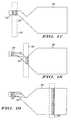
- FIGS. 5-10are top views of a sample structure at sequential stages in a first variant of processing the semiconductor layer on the substrate to form single-crystal regions;
- FIGS. 11-16are top views of a sample structure at sequential stages in a second variant of processing the semiconductor layer on the substrate to form single-crystal regions;
- FIGS. 17-19are top views of a sample structure at sequential stages in a third variant of processing the semiconductor layer on the substrate to form single-crystal regions;
- FIG. 20illustrates graphically the relationship between maximum attainable film thickness and lattice mismatch between a host crystal and a grown crystalline overlayer
- FIG. 21illustrates a high resolution Transmission Electron Micrograph of a structure including a monocrystalline accommodating buffer layer
- FIG. 22illustrates an x-ray diffraction spectrum of a structure including a monocrystalline accommodating buffer layer
- FIG. 23illustrates a high resolution Transmission Electron Micrograph of a structure including an amorphous oxide layer
- FIG. 24illustrates an x-ray diffraction spectrum of a structure including an amorphous oxide layer
- FIGS. 25-28illustrate schematically, in cross-section, the formation of a device structure suitable for lighting devices in accordance with another embodiment of the invention.
- FIGS. 29-32illustrate a probable molecular bonding structure of the device structures illustrated in FIGS. 25-28;
- FIGS. 33-36illustrate schematically, in cross-section, the formation of a device structure suitable for forming lighting sources in accordance with still another embodiment of the invention
- FIGS. 37-39illustrate schematically, in cross-section, the formation of yet another embodiment of a device structure suitable for lighting sources in accordance with the invention
- FIGS. 40, 41illustrate schematically, in cross section, device structures that can be used for light devices in accordance with various embodiments of the invention
- FIGS. 42-46are illustrations of cross-sectional views of a portion of an integrated circuit that includes a compound semiconductor portion, a bipolar portion, and an MOS portion;
- FIGS. 47-53are illustrations of cross-sectional views of a portion of another integrated circuit that includes a semiconductor laser and a MOS transistor in accordance with various embodiments of the invention.
- FIG. 54illustrates schematically, in cross-section, a portion of a light source device in accordance with an embodiment of the invention.
- FIG. 55illustrates schematically, in cross-section, a portion of a full-color display device in accordance with a further embodiment of the invention.
- FIG. 56is a flow chart that shows a process for fabricating a structure for producing light.
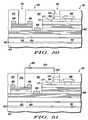
- FIG. 1illustrates schematically, in cross section, a portion of a semiconductor structure 20 suitable for providing light sources in accordance with an embodiment of the invention.
- Semiconductor structure 20includes a substrate 21 , a thermal oxide layer 23 , a monocrystalline semiconductor layer 22 , accommodating buffer layer 24 comprising a monocrystalline material, and a monocrystalline material layer 26 .
- the term “monocrystalline”shall have the meaning commonly used within the semiconductor industry.
- the termshall refer to materials that are a single crystal or that are substantially a single crystal and shall include those materials having a relatively small number of defects such as dislocations and the like as are commonly found in bulk substrates of silicon or germanium or mixtures of silicon and germanium and epitaxial layers of such materials commonly found in the semiconductor industry.
- Structure 20can also include an amorphous intermediate layer 28 positioned between semiconductor layer 22 and accommodating buffer layer 24 .
- Structure 20may also include a template layer 30 between the accommodating buffer layer and monocrystalline material layer 26 .
- the template layerhelps to initiate the growth of the monocrystalline material layer on the accommodating buffer layer.
- the amorphous intermediate layerhelps to relieve the strain in the accommodating buffer layer and by doing so, aids in the growth of a high crystalline quality accommodating buffer layer.
- the substrate 21can be any suitable material, e.g., silicon, quartz, glass or plastic, or the like, subject to considerations of stability, inertness and heat resistance under processing conditions.
- the substrate 21is glass.
- the term “substrate”is normally used to indicate either the substrate 21 or the structure including the substrate 21 , the oxide layer 23 , and the semiconductor layer 22 .
- the substrate 21is alternatively called a glass substrate, although it can be formed of other materials, as described herein.
- the structure including the substrate 21 , the oxide layer 23 , and the semiconductor layer 22is alternatively called a monocrystalline substrate, or a silicon substrate (the silicon substrate being one form of the monocrystalline substrate).
- the term monocrystalline substraterefers to a bulk monocrystalline substrate
- the term silicon substratemeans a bulk silicon substrate.
- the term compliant substrategenerally refers to the monocrystilline substrate with the accommodating buffer layer 24 formed thereon.
- the thermal oxide layer 23is preferably a layer of silicon dioxide formed or deposited on the surface of the substrate 21 .
- Semiconductor layer 22can be a monocrystalline semiconductor or compound semiconductor film formed on the thermal oxide layer 23 on the substrate 21 .
- the filmcan be, for example, a material from Group IV of the periodic table. Examples of Group IV semiconductor materials include silicon, germanium, mixed silicon and germanium, mixed silicon and carbon, mixed silicon, germanium and carbon, and the like.
- layer 22is a film of deposited silicon. The process of forming regions of the monocrystalline semiconductor layer 22 on the substrate 21 is described below in connection with FIGS. 4-19.
- Accommodating buffer layer 24is preferably a monocrystalline oxide or nitride material epitaxially grown on layer 22 .
- Amorphous intermediate layer 28can be grown on layer 22 at the interface between semiconductor layer 22 and the growing accommodating buffer layer by the oxidation of semiconductor layer 22 during the growth of layer 24 .
- the amorphous intermediate layerserves to relieve strain that might otherwise occur in the monocrystalline accommodating buffer layer as a result of differences in the lattice constants of the material of layer 22 and the buffer layer.
- lattice constantrefers to the distance between atoms of a cell measured in the plane of the surface. If such strain is not relieved by the amorphous intermediate layer, the strain may cause defects in the crystalline structure of the accommodating buffer layer.
- monocrystalline material layer 26which may comprise a semiconductor material, a compound semiconductor material, or another type of material such as a metal or a non-metal.
- Accommodating buffer layer 24is preferably a monocrystalline oxide or nitride material selected for its crystalline compatibility with the underlying monocrystalline substrate and with the overlying material layer.
- the materialcould be an oxide or nitride having a lattice structure closely matched to the monocrystalline layer and to the subsequently applied monocrystalline material layer.
- Materials that are suitable for the accommodating buffer layerinclude metal oxides such as the alkaline earth metal titanates, alkaline earth metal zirconates, alkaline earth metal hafnates, alkaline earth metal tantalates, alkaline earth metal ruthenates, alkaline earth metal niobates, alkaline earth metal vanadates, alkaline earth metal tin-based perovskites, lanthanum aluminate, lanthanum scandium oxide, and gadolinium oxide. Additionally, various nitrides such as gallium nitride, aluminum nitride, and boron nitride may also be used for the accommodating buffer layer.
- metal oxidessuch as the alkaline earth metal titanates, alkaline earth metal zirconates, alkaline earth metal hafnates, alkaline earth metal tantalates, alkaline earth metal ruthenates, alkaline earth metal niobates, alkaline earth metal vanadates, alkaline earth metal tin
- these materialsare insulators, although strontium ruthenate, for example, is a conductor.
- these materialsare metal oxides or metal nitrides, and more particularly, these metal oxide or nitrides typically include at least two different metallic elements. In some specific applications, the metal oxides or nitrides may include three or more different metallic elements.
- Amorphous interface layer 28is preferably an oxide formed by the oxidation of the surface of semiconductor layer 22 , and more preferably is composed of a silicon oxide.
- the thickness of layer 28is sufficient to relieve strain attributed to mismatches between the lattice constants of semiconductor layer 22 and accommodating buffer layer 24 .
- layer 28has a thickness in the range of approximately 0.5-5 nm.
- the material for monocrystalline material layer 26can be selected, as desired, for a particular structure or application.
- the monocrystalline material of layer 26may comprise a compound semiconductor which can be selected, as needed for a particular semiconductor structure, from any of the Group IIIA and VA elements (III-V semiconductor compounds), mixed III-V compounds, Group II(A or B) and VIA elements (II-VI semiconductor compounds), and mixed II-VI compounds.
- monocrystalline material layer 26may also comprise other semiconductor materials, metals, or non-metal materials which are used in the formation of semiconductor structures, devices and/or integrated circuits.
- template 30Appropriate materials for template 30 are discussed below. Suitable template materials chemically bond to the surface of the accommodating buffer layer 24 at selected sites and provide sites for the nucleation of the epitaxial growth of monocrystalline material layer 26 . When used, template layer 30 has a thickness ranging from about 1 to about 10 monolayers.
- FIG. 2illustrates, in cross section, a portion of a semiconductor structure 40 suitable for constructing lighting sources in accordance with a further embodiment of the invention.
- Structure 40is similar to the previously described semiconductor structure 20 , except that an additional buffer layer 32 is positioned between accommodating buffer layer 24 and monocrystalline material layer 26 .
- the additional buffer layeris positioned between template layer 30 and the overlying layer of monocrystalline material.
- the additional buffer layerformed of a semiconductor or compound semiconductor material when the monocrystalline material layer 26 comprises a semiconductor or compound semiconductor material, serves to provide a lattice compensation when the lattice constant of the accommodating buffer layer cannot be adequately matched to the overlying monocrystalline semiconductor or compound semiconductor material layer.
- FIG. 3schematically illustrates, in cross section, a portion of a semiconductor structure 34 suitable for constructing lighting devices in accordance with another exemplary embodiment of the invention.
- Structure 34is similar to structure 20 , except that structure 34 includes an amorphous layer 36 , rather than accommodating buffer layer 24 and amorphous interface layer 28 , and an additional monocrystalline layer 38 .
- amorphous layer 36may be formed by first forming an accommodating buffer layer and an amorphous interface layer in a similar manner to that described above. Monocrystalline layer 38 is then formed (by epitaxial growth) overlying the monocrystalline accommodating buffer layer. The accommodating buffer layer is then exposed to an anneal process to convert the monocrystalline accommodating buffer layer to an amorphous layer. Amorphous layer 36 formed in this manner comprises materials from both the accommodating buffer and interface layers, which amorphous layers may or may not amalgamate. Thus, layer 36 may comprise one or two amorphous layers. Formation of amorphous layer 36 between semiconductor layer 22 and additional monocrystalline layer 26 (subsequent to layer 38 formation) relieves stresses between layers 22 and 38 and provides a true compliant substrate for subsequent processing—e.g., monocrystalline material layer 26 formation.
- Additional monocrystalline layer 38may include any of the materials described throughout this application in connection with either of monocrystalline material layer 26 or additional buffer layer 32 .
- layer 38may include monocrystalline Group IV or monocrystalline compound semiconductor materials.
- Additional monocrystalline layer 38can serve as an anneal cap during layer 36 formation and as a template for subsequent monocrystalline layer 26 formation. Accordingly, layer 38 is preferably thick enough to provide a suitable template for layer 26 growth (at least one monolayer) and thin enough to allow layer 38 to form as a substantially defect free monocrystalline material.
- additional monocrystalline layer 38can comprise monocrystalline material (e.g., a material discussed above in connection with monocrystalline layer 26 ) that is thick enough to form devices within layer 38 .
- the semiconductor structuredoes not include monocrystalline material layer 26 .
- the semiconductor structure in accordance with this embodimentonly includes one monocrystalline layer disposed above amorphous oxide layer 36 .
- FIGS. 4-19one process by which the monocrystalline semiconductor layer 22 is formed on the substrate 21 is described in further detail.
- a lateral solidification techniqueis applied to a semiconductor film on the substrate 21 .
- the techniqueinvolves irradiating a portion of the film with a suitable radiation pulse, e.g., a laser beam pulse, locally, to melt the film completely through its entire thickness.
- a suitable radiation pulsee.g., a laser beam pulse
- a beamis pulsed repeatedly in forming an extended single-crystal region as a result of laterally stepping a radiation pattern for repeated melting and solidification.
- the technique described herein for forming layer 22 over substrate 21is similar to a technique described in International Patent Application number PCT/US96/07730. Any other technique that results in a monocrystalline semiconductor layer over glass can be used to form the semiconductor layer 22 .
- FIG. 4illustrates a block diagram of a projection irradiation system 510 for forming the monocrystalline regions on the glass substrate.
- the projection irradiation systemincludes an excimer laser 501 , mirrors 502 , a variable focus field lens 504 , a patterned mask 505 , a two-element imaging lens 506 , a sample stage 507 , and a variable attenuator 508 .
- a sample 500is disposed on the sample stage 507 .
- This systemcan be used to produce a shaped beam for stepped growth of a single-crystal silicon region in a sequential lateral solidification (SLS) process.
- SLSsequential lateral solidification
- a proximity mask or even a contact maskmay be used for beam shaping.
- samplesare placed onto the stage 507 of the projection irradiation system 510 .
- the maskcan have a pattern of simple stripes of 50 micrometers wide, with various separation distances from 10 to 100 micrometers.
- radiation beams other than a laser beamcan be used, for example, an electron or ion beam.
- the sample structureincludes the substrate 21 , a thermal oxide film 23 , and an amorphous silicon film deposited over the thermal oxide film 23 .
- Structures in accordance with layers 22 - 23can prepared by any suitable conventional processing technique, including sequential low-pressure chemical vapor deposition (LPCVD) of SiO 2 and a —Si on a glass or quartz substrate.
- LPCVDsequential low-pressure chemical vapor deposition
- Other suitable deposition methods, for producing amorphous or microcrystalline depositsinclude plasma-enhanced chemical vapor deposition (PECVD), evaporation or sputtering, for example.
- PECVDplasma-enhanced chemical vapor deposition
- evaporation or sputteringfor example.
- the mask patternis projected onto the samples with different reduction factors in the range from 3 to 6.
- Samplescan be irradiated at room temperature with a 30-nanosecond XeCl excimer laser pulse having a wavelength of 308 nanometers, quartz being transparent at this wavelength.
- a laseris commercially available.
- a longer wavelengthcan be used, e.g., 348 nanometers.
- Irradiationcan be with fixed energy density.
- the energy densitycan be in the range from 1 to 680 mJ/cm 2 .
- the sequential lateral solidification (SLS) processis described with reference to FIGS. 5-10 and 11 - 16 showing first and second variants, respectively, of the process, and FIGS. 17-19 showing a third variant.
- a region 520bounded by two broken lines, of the silicon film 521 is irradiated with a pulse, to completely melt the silicon in that region (FIG. 6 ), and then resolidify the molten silicon (FIG. 7) in the region 520 .
- the region 520is in the shape of a stripe, and irradiation of the region 520 may be masked projection or by use of a proximity mask.
- the width of the stripeis chosen such that, upon resolidification, the two rows of grains approach each other without converging. Smaller widths of the region 520 tend to be undesirable since the subsequent step may have to be reduced in length, and the semiconductor surface may become irregular where grains growing from opposite directions come together during the solidification process.
- An oxide capmay be formed over the silicon film to retard agglomeration and constrain the surface of the silicon film to be smooth.
- a next region 526 to be irradiatedis defined by shifting (stepping) the sample with respect to the masked projection or proximity mask in the direction of crystal growth.
- the shifted (stepped) region 526is bounded by two broken lines, as shown in FIG. 8 .
- the distance of the shiftis such that the next region 526 to be irradiated overlaps the previously irradiated region 520 so as to completely melt one row of crystals 522 while partially melting the other row of crystals 522 , as shown in FIG. 9 .
- the partially melted row of crystalsbecomes longer, as shown in FIG. 10 .
- monocrystalline grains of any desired lengthmay be grown.
- the pattern of the irradiated regionis not a simple stripe, but is in the shape of a chevron 540 , as shown in FIG. 11, the same sequence of shifting the irradiated region shown in FIGS. 12-16 results in the enlargement of one grain growing from the apex of the trailing edge of the shifting (stepping) chevron pattern. In this manner, a monocrystalline region 571 can be grown with increasing width and length.
- a large area single-crystal regioncan also be grown by applying sequentially shifted (stepped) irradiation regions to a patterned amorphous silicon film, such as that illustrated in FIG. 17, having a tail region 550 , a narrow bottleneck region 552 and a main island region 554 .
- the region of irradiation 553 defined by masked projection or a proximity maskis illustrated by the regions bounded by broken lines in FIGS. 17-19, which also show the sequential lateral shifting (stepping) of the irradiated region 553 to obtain the growth of a single grain from the tail region 550 through the bottleneck region 552 to produce a single crystal island region 554 .
- Sequential lateral melting and resolidification in the examples of FIGS. 5-10, 11 - 16 and 17 - 19can be carried out on amorphous silicon films that are deposited by chemical vapor deposition (CVD) on a silicon dioxide coated quartz or glass substrate, with film thicknesses from 100 to 240 nanometers.
- CVDchemical vapor deposition
- monocrystalline semiconductor layer 22is a silicon film oriented in the (100) direction.
- the silicon filmcan be, for example, a silicon layer as is used in making complementary metal oxide semiconductor (CMOS) integrated circuits.
- accommodating buffer layer 24is a monocrystalline layer of Sr 2 Ba l ⁇ z TiO 3 where z ranges from 0 to 1 and the amorphous intermediate layer is a layer of silicon oxide (SiO x ) formed at the interface between the silicon film and the accommodating buffer layer. The value of z is selected to obtain one or more lattice constants closely matched to corresponding lattice constants of the subsequently formed layer 26 .
- the accommodating buffer layercan have a thickness of about 2 to about 100 nanometers (nm) and preferably has a thickness of about 5 nm. In general, it is desired to have an accommodating buffer layer thick enough to isolate the monocrystalline material layer 26 from the silicon layer to obtain the desired electrical and optical properties. Layers thicker than 100 nm usually provide little additional benefit while increasing cost unnecessarily; however, thicker layers may be fabricated if needed.
- the amorphous intermediate layer of silicon oxidecan have a thickness of about 0.5-5 nm, and preferably a thickness of about 1 to 2 nm.
- Monocrystalline material layer 26is a compound semiconductor layer of gallium arsenide (GaAs) or aluminum gallium arsenide (AlGaAs) having a thickness of about 1 nm to about 100 micrometers ( ⁇ m) and preferably a thickness of about 0.5 ⁇ m to 10 ⁇ m. The thickness generally depends on the application for which the layer is being prepared.
- a template layeris formed by capping the oxide layer.
- the template layeris preferably 1-10 monolayers of Ti—As, Sr—O—As, Sr—Ga—O, or Sr—Al—O.
- 1-2 monolayers of Ti—As or Sr—Ga—Ohave been illustrated to successfully grow GaAs layers.
- monocrystalline semiconductor layer 22is a silicon film as described above.
- the accommodating buffer layeris a monocrystalline oxide of strontium or barium zirconate or hafnate in a cubic or orthorhombic phase with an amorphous intermediate layer of silicon oxide formed at the interface between the silicon layer and the accommodating buffer layer.
- the accommodating buffer layercan have a thickness of about 2-100 nm and preferably has a thickness of at least 5 nm to ensure adequate crystalline and surface quality and is formed of a monocrystalline SrZrO 3 , BaZrO 3 , SrHfO 3 , BaSnO 3 or BaHfO 3 .
- a monocrystalline oxide layer of BaZrO 3can grow at a temperature of about 700 degrees C.
- the lattice structure of the resulting crystalline oxideexhibits a 45 degree rotation with respect to the silicon film lattice structure.
- an accommodating buffer layer formed of these zirconate or hafnate materialsis suitable for the growth of a monocrystalline material layer which comprises compound semiconductor materials in the indium phosphide (InP) system.
- the compound semiconductor materialcan be, for example, indium phosphide (InP), indium gallium arsenide (InGaAs), aluminum indium arsenide, (AlInAs), or aluminum gallium indium arsenic phosphide (AlGaInAsP), having a thickness of about 1.0 nm to 10 ⁇ m.
- a suitable template for this structureis 1-10 monolayers of zirconium-arsenic (Zr—As), zirconium-phosphorus (Zr—P), hafnium-arsenic (Hf—As), hafnium-phosphorus (Hf—P), strontium-oxygen-arsenic (Sr—O—As), strontium-oxygen-phosphorus (Sr—O—P), barium-oxygen-arsenic (Ba—O—As), indium-strontium-oxygen (In—Sr—O), or barium-oxygen-phosphorus (Ba—O—P), and preferably 1-2 monolayers of one of these materials.
- the surfaceis terminated with 1-2 monolayers of zirconium followed by deposition of 1-2 monolayers of arsenic to form a Zr—As template.
- a monocrystalline layer of the compound semiconductor material from the indium phosphide systemis then grown on the template layer.
- the resulting lattice structure of the compound semiconductor materialexhibits a 45 degree rotation with respect to the accommodating buffer layer lattice structure and a lattice mismatch to (100) InP of less than 2.5%, and preferably less than about 1.0%.
- a structureis provided that is suitable for the growth of an epitaxial film of a monocrystalline material comprising a II-VI material overlying a silicon film on the glass substrate.
- a suitable accommodating buffer layer materialis Sr x Ba l ⁇ x TiO 3 , where x ranges from 0 to 1, having a thickness of about 2-100 nm and preferably a thickness of about 5-15 nm.
- the II-VI compound semiconductor materialcan be, for example, zinc selenide (ZnSe) or zinc sulfur selenide (ZnSSe).
- a suitable template for this material systemincludes 1-10 monolayers of zinc-oxygen (Zn—O) followed by 1-2 monolayers of an excess of zinc followed by the selenidation of zinc on the surface.
- a templatecan be, for example, 1-10 monolayers of strontium-sulfur (Sr—S) followed by the ZnSeS.
- This embodiment of this example ofis shown as structure 40 illustrated in FIG. 2 .
- Semiconductor layer 22 , accommodating buffer layer 24 , and monocrystalline material layer 26can be similar to those described in Example 1.
- an additional buffer layer 32serves to alleviate any strains that might result from a mismatch of the crystal lattice of the accommodating buffer layer and the lattice of the monocrystalline material.
- Buffer layer 32can be a layer of germanium or a GaAs, an aluminum gallium arsenide (AlGaAs), an indium gallium phosphide (InGaP), an aluminum gallium phosphide (AlGaP), an indium gallium arsenide (InGaAs), an aluminum indium phosphide (AlInP), a gallium arsenide phosphide (GaAsP), or an indium gallium phosphide (InGaP) strain compensated superlattice.
- buffer layer 32includes a GaAs x P l ⁇ x superlattice, wherein the value of x ranges from 0 to 1.
- buffer layer 32includes an In y Ga l ⁇ y P superlattice, wherein the value of y ranges from 0 to 1.
- the lattice constantis varied from bottom to top across the superlattice to create a match between lattice constants of the underlying oxide and the overlying monocrystalline material which in this example is a compound semiconductor material.
- the compositions of other compound semiconductor materials, such as those listed above,may also be similarly varied to manipulate the lattice constant of layer 32 in a like manner.
- the superlatticecan have a thickness of about 50-500 nm and preferably has a thickness of about 100-200 nm.
- buffer layer 32can be a layer of monocrystalline germanium having a thickness of 1-50 nm and preferably having a thickness of about 2-20 nm.
- a template layer of either germanium-strontium (Ge—Sr) or germanium-titanium (Ge—Ti) having a thickness of about one monolayercan be used as a nucleating site for the subsequent growth of the monocrystalline material layer which in this example is a compound semiconductor material.
- the formation of the oxide layeris capped with either a monolayer of strontium or a monolayer of titanium to act as a nucleating site for the subsequent deposition of the monocrystalline germanium.
- the monolayer of strontium or titaniumprovides a nucleating site to which the first monolayer of germanium can bond.
- This examplealso illustrates materials useful in a structure 40 as illustrated in FIG. 2 .
- Semiconductor material 22 , accommodating buffer layer 24 , monocrystallinematerial layer 26 and template layer 30can be the same as those described above in Example 2.
- additional buffer layer 32is inserted between the accommodating buffer layer and the overlying monocrystalline material layer.
- the buffer layera further monocrystalline material which in this instance comprises a semiconductor material, can be, for example, a graded layer of indium gallium arsenide (InGaAs) or indium aluminum arsenide (InAlAs).
- additional buffer layer 32includes InGaAs, in which the indium composition varies from 0 to about 50%.
- the additional buffer layer 32preferably has a thickness of about 10-30 nm. Varying the composition of the buffer layer from GaAs to InGaAs serves to provide a lattice match between the underlying monocrystalline oxide material and the overlying layer of monocrystalline material which in this example is a compound semiconductor material. Such a buffer layer is especially advantageous if there is a lattice mismatch between accommodating buffer layer 24 and monocrystalline material layer 26 .
- This exampleprovides exemplary materials useful in structure 34 , as illustrated in FIG. 3 .
- Semiconductor material 22 , template layer 30 , and monocrystalline material layer 26may be the same as those described above in connection with example 1.
- Amorphous layer 36is an amorphous oxide layer which is suitably formed of a combination of amorphous intermediate layer materials (e.g., layer 28 materials as described above) and accommodating buffer layer materials (e.g., layer 24 materials as described above).
- amorphous layer 36may include a combination of SiO x and Sr z Ba l ⁇ z TiO 3 (where z ranges from 0 to 1),which combine or mix, at least partially, during an anneal process to form amorphous oxide layer 36 .
- amorphous layer 36may vary from application to application and may depend on such factors as desired insulating properties of layer 36 , type of monocrystalline material comprising layer 26 , and the like. In accordance with one exemplary aspect of the present embodiment, layer 36 thickness is about 2 nm to about 100 nm, preferably about 2-10 nm, and more preferably about 5-6 nm.
- Layer 38comprises a monocrystalline material that can be grown epitaxially over a monocrystalline oxide material such as material used to form accommodating buffer layer 24 .
- Layer 38can include the same materials as those comprising layer 26 .
- layer 38also includes GaAs.
- layer 38may include materials different from those used to form layer 26 .
- layer 38is about 1 monolayer to about 100 nm thick.
- semiconductor layer 22is a monocrystalline region of film, such as a monocrystalline silicon.
- the crystalline structure of the monocrystalline filmis characterized by a lattice constant and by a lattice orientation.
- accommodating buffer layer 24is also a monocrystalline material and the lattice of that monocrystalline material is characterized by a lattice constant and a crystal orientation.
- the lattice constants of the accommodating buffer layer and the monocrystalline layer 22must be closely matched or, alternatively, must be such that upon rotation of one crystal orientation with respect to the other crystal orientation, a substantial match in lattice constants is achieved.
- the terms “substantially equal” and “substantially matched”mean that there is sufficient similarity between the lattice constants to permit the growth of a high quality crystalline layer on the underlying layer.
- FIG. 20illustrates graphically the relationship of the achievable thickness of a grown crystal layer of high crystalline quality as a function of the mismatch between the lattice constants of the host crystal and the grown crystal.
- Curve 42illustrates the boundary of high crystalline quality material. The area to the right of curve 42 represents layers that have a large number of defects. With no lattice mismatch, it is theoretically possible to grow an infinitely thick, high quality epitaxial layer on the host crystal. As the mismatch in lattice constants increases, the thickness of achievable, high quality crystalline layer decreases rapidly.
- semiconductor layer 22can be a (100) or (111) oriented monocrystalline silicon and accommodating buffer layer 24 is a layer of strontium barium titanate. Substantial matching of lattice constants between these two materials is achieved by rotating the crystal orientation of the titanate material by 45° with respect to the crystal orientation of the silicon.
- a silicon oxide layer in this exampleserves to reduce strain in the titanate monocrystalline layer that might result from any mismatch in the lattice constants of the host silicon and the grown titanate layer. As a result, a high quality, thick, monocrystalline titanate layer is achievable.
- layer 26is a layer of epitaxially grown monocrystalline material and that crystalline material is also characterized by a crystal lattice constant and a crystal orientation.
- the lattice constant of layer 26can differ from the lattice constant of semiconductor layer 22 .
- the accommodating buffer layermust be of high crystalline quality.
- substantial matching between the crystal lattice constant of the host crystal, in this case, the monocrystalline accommodating buffer layer, and the grown crystalis desired. With properly selected materials this substantial matching of lattice constants is achieved as a result of rotation of the crystal orientation of the grown crystal with respect to the orientation of the host crystal.
- the grown crystalis gallium arsenide, aluminum gallium arsenide, zinc selenide, or zinc sulfur selenide and the accommodating buffer layer is monocrystalline Sr x Ba l ⁇ x TiO 3 , substantial matching of crystal lattice constants of the two materials is achieved, wherein the crystal orientation of the grown layer is rotated by 45° with respect to the orientation of the host monocrystalline oxide.
- the host materialis a strontium or barium zirconate or a strontium or barium hafnate or barium tin oxide and the compound semiconductor layer is indium phosphide or gallium indium arsenide or aluminum indium arsenide
- substantial matching of crystal lattice constantscan be achieved by rotating the orientation of the grown crystal layer by 45° with respect to the host oxide crystal.
- a crystalline semiconductor buffer layer between the host oxide and the grown monocrystalline material layercan be used to reduce strain in the grown monocrystalline material layer that might result from small differences in lattice constants. Better crystalline quality in the grown monocrystalline material layer can thereby be achieved.
- the following exampleillustrates a process for fabricating a semiconductor structure such as the structures depicted in FIGS. 1-3.
- the processstarts by providing a glass substrate having formed thereon regions of single-crystal (monocrystalline) silicon.
- the monocrystalline silicon regionshave a (100) orientation.
- the silicon regionsare preferably oriented on axis or, at most, about 4° off axis.
- At least a portion of the silicon substratehas a bare surface, although other portions of the silicon substrate, as described below, may encompass other structures.
- the term “bare” in this contextmeans that the surface in the portions of the silicon substrate has been cleaned to remove any oxides, contaminants, or other foreign material.
- the native oxide layerIn order to epitaxially grow a monocrystalline oxide layer overlying the monocrystalline silicon film, the native oxide layer must first be removed to expose the crystalline structure of the underlying film.
- the following processis preferably carried out by molecular beam epitaxy (MBE), although other epitaxial processes may also be used in accordance with the present invention.
- MBEmolecular beam epitaxy
- the native oxidecan be removed by first thermally depositing a thin layer of strontium, barium, a combination of strontium and barium, or other alkaline earth metals or combinations of alkaline earth metals in an MBE apparatus. In the case where strontium is used, the silicon substrate is then heated to a temperature of about 750° C. to cause the strontium to react with the native silicon oxide layer.
- the strontiumserves to reduce the silicon oxide to leave a silicon oxide-free surface.
- the resultant surfacewhich exhibits an ordered 2 ⁇ 1 structure, includes strontium, oxygen, and silicon.
- the ordered 2 ⁇ 1 structureforms a template for the ordered growth of an overlying layer of a monocrystalline oxide.
- the templateprovides the necessary chemical and physical properties to nucleate the crystalline growth of an overlying layer.
- the native silicon oxidecan be converted and the film surface can be prepared for the growth of a monocrystalline oxide layer by depositing an alkaline earth metal oxide, such as strontium oxide, strontium barium oxide, or barium oxide, onto the silicon substrate surface by MBE at a low temperature and by subsequently heating the structure to a temperature of about 750° C. At this temperature, a solid state reaction takes place between the strontium oxide and the native silicon oxide causing the reduction of the native silicon oxide and leaving an ordered 2 ⁇ 1 structure with strontium, oxygen, and silicon remaining on the silicon substrate surface. Again, this forms a template for the subsequent growth of an ordered monocrystalline oxide layer.
- an alkaline earth metal oxidesuch as strontium oxide, strontium barium oxide, or barium oxide
- the silicon substrateis cooled to a temperature in the range of about 200-800° C. and a layer of strontium titanate is grown on the template layer by molecular beam epitaxy.
- the MBE processis initiated by opening shutters in the MBE apparatus to expose strontium, titanium and oxygen sources.
- the ratio of strontium and titaniumis approximately 1:1.
- the partial pressure of oxygenis initially set at a minimum value to grow stoichiometric strontium titanate at a growth rate of about 0.3-0.5 nm per minute. After initiating growth of the strontium titanate, the partial pressure of oxygen is increased above the initial minimum value.
- the overpressure of oxygencauses the growth of an amorphous silicon oxide layer at the interface between the underlying monocrystalline layer and the growing strontium titanate layer.
- the growth of the silicon oxide layerresults from the diffusion of oxygen through the growing strontium titanate layer to the interface where the oxygen reacts with silicon at the surface of the underlying silicon substrate.
- the strontium titanategrows as an ordered (100) monocrystal with the (100) crystalline orientation rotated by 45° with respect to the underlying silicon substrate. Strain that otherwise might exist in the strontium titanate layer because of the small mismatch in lattice constant between the silicon substrate and the growing crystal is relieved in the amorphous silicon oxide intermediate layer.
- the monocrystalline strontium titanateis capped by a template layer that is conducive to the subsequent growth of an epitaxial layer of a desired monocrystalline material.
- the MBE growth of the strontium titanate monocrystalline layercan be capped by terminating the growth with 1-2 monolayers of titanium, 1-2 monolayers of titanium-oxygen or with 1-2 monolayers of strontium-oxygen.
- arsenicis deposited to form a Ti—As bond, a Ti—O—As bond or a Sr—O—As.
- gallium arsenide monocrystalline layeris subsequently introduced to the reaction with the arsenic and gallium arsenide forms.
- galliumcan be deposited on the capping layer to form a Sr—O—Ga bond, and arsenic is subsequently introduced with the gallium to form the GaAs.
- FIG. 21is a high resolution Transmission Electron Micrograph (TEM) of semiconductor material using a bulk silicon substrate. Similar results are predicted for material manufactured using a monocrystalline silicon film formed over a glass layer.
- Single crystal SrTiO 3 accommodating buffer layer 24was grown epitaxially on silicon semiconductor layer 22 . During this growth process, amorphous interfacial layer 28 is formed which relieves strain due to lattice mismatch.
- GaAs compound semiconductor layer 26was then grown epitaxially using template layer 30 .
- FIG. 22illustrates an x-ray diffraction spectrum taken on a structure including GaAs monocrystalline layer 26 comprising GaAs grown on a bulk silicon substrate using accommodating buffer layer 24 . Similar results are predicted for material manufactured using a monocrystalline silicon film formed over a glass layer. The peaks in the spectrum indicate that both the accommodating buffer layer 24 and GaAs compound semiconductor layer 26 are single crystal and (100) orientated.
- the structure illustrated in FIG. 2can be formed by the process discussed above with the addition of an additional buffer layer deposition step.
- the additional buffer layer 32is formed overlying the template layer before the deposition of the monocrystalline material layer. If the buffer layer is a monocrystalline material comprising a compound semiconductor superlattice, such a superlattice can be deposited, by MBE for example, on the template described above. If instead the buffer layer is a monocrystalline material layer comprising a layer of germanium, the process above is modified to cap the strontium titanate monocrystalline layer with a final layer of either strontium or titanium and then by depositing germanium to react with the strontium or titanium. The germanium buffer layer can then be deposited directly on this template. Structure 34 , illustrated in FIG.
- the accommodating buffer layermay be formed by growing an accommodating buffer layer, forming an amorphous oxide layer over semiconductor layer 22 , and growing semiconductor layer 38 over the accommodating buffer layer, as described above.
- the accommodating buffer layer and the amorphous oxide layerare then exposed to an anneal process sufficient to change the crystalline structure of the accommodating buffer layer from monocrystalline to amorphous, thereby forming an amorphous layer such that the combination of the amorphous oxide layer and the now amorphous accommodating buffer layer form a single amorphous oxide layer 36 .
- Layer 26is then subsequently grown over layer 38 .
- the anneal processmay be carried out subsequent to growth of layer 26 .
- layer 36is formed by exposing semiconductor layer 22 , the accommodating buffer layer, the amorphous oxide layer, and monocrystalline layer 38 to a rapid thermal anneal process with a peak temperature of about 700° C. to about 1000° C. and a process time of about 5 seconds to about 10 minutes.
- suitable anneal processesmay be employed to convert the accommodating buffer layer to an amorphous.
- laser annealing, electron beam annealing, or “conventional” thermal annealing processesin the proper environment
- an overpressure of one or more constituents of layer 30may be required to prevent degradation of layer 38 during the anneal process.
- the anneal environmentpreferably includes an overpressure of arsenic to mitigate degradation of layer 38 .
- layer 38 of structure 34may include any materials suitable for either of layers 32 or 26 . Accordingly, any deposition or growth methods described in connection with either layer 32 or 26 , may be employed to deposit layer 38 .
- FIG. 23is a high resolution TEM of semiconductor material manufactured in accordance with the structure illustrated in FIG. 3, but using a bulk substrate. Similar results are predicted for material manufactured using a monocrystalline silicon film formed over a glass layer.
- a single crystal SrTiO 3 accommodating buffer layerwas grown epitaxially on the bulk substrate. During this growth process, an amorphous interfacial layer forms as described above.
- additional monocrystalline layer 38comprising a compound semiconductor layer of GaAs is formed above the accommodating buffer layer and the accommodating buffer layer is exposed to an anneal process to form amorphous oxide layer 36 .
- FIG. 24illustrates an x-ray diffraction spectrum taken on a structure including additional monocrystalline layer 38 comprising a GaAs compound semiconductor layer and amorphous oxide layer 36 formed on a bulk substrate. Similar results are predicted for material manufactured using a monocrystalline silicon film formed over a glass layer. The peaks in the spectrum indicate that GaAs compound semiconductor layer 38 is single crystal and (100) orientated and the lack of peaks around 40 to 50 degrees indicates that layer 36 is amorphous.
- the process described aboveillustrates a process for forming a semiconductor structure including a silicon substrate, an overlying oxide layer, and a monocrystalline material layer comprising a gallium arsenide compound semiconductor layer by the process of molecular beam epitaxy.
- the processcan also be carried out by the process of chemical vapor deposition (CVD), metal organic chemical vapor deposition (MOCVD), migration enhanced epitaxy (MEE), atomic layer epitaxy (ALE), physical vapor deposition (PVD), chemical solution deposition (CSD), pulsed laser deposition (PLD), or the like.
- CVDchemical vapor deposition
- MOCVDmetal organic chemical vapor deposition
- MEEmigration enhanced epitaxy
- ALEatomic layer epitaxy
- PVDphysical vapor deposition
- CSSDchemical solution deposition
- PLDpulsed laser deposition
- monocrystalline accommodating buffer layerssuch as alkaline earth metal titanates, zirconates, hafnates, tantalates, vanadates, ruthenates, and niobates, alkaline earth metal tin-based perovskites, lanthanum aluminate, lanthanum scandium oxide, and gadolinium oxide can also be grown.
- a similar processsuch as MBE, other monocrystalline material layers comprising other III-V and II-VI monocrystalline compound semiconductors, semiconductors, metals and non-metals can be deposited overlying the monocrystalline oxide accommodating buffer layer.
- each of the variations of monocrystalline material layer and monocrystalline oxide accommodating buffer layeruses an appropriate template for initiating the growth of the monocrystalline material layer.
- the accommodating buffer layeris an alkaline earth metal zirconate
- the oxidecan be capped by a thin layer of zirconium.
- the deposition of zirconiumcan be followed by the deposition of arsenic or phosphorus to react with the zirconium as a precursor to depositing indium gallium arsenide, indium aluminum arsenide, or indium phosphide respectively.
- the monocrystalline oxide accommodating buffer layeris an alkaline earth metal hafnate, the oxide layer can be capped by a thin layer of hafnium.
- hafniumis followed by the deposition of arsenic or phosphorous to react with the hafnium as a precursor to the growth of an indium gallium arsenide, indium aluminum arsenide, or indium phosphide layer, respectively.
- strontium titanatecan be capped with a layer of strontium or strontium and oxygen and barium titanate can be capped with a layer of barium or barium and oxygen.
- Each of these depositionscan be followed by the deposition of arsenic or phosphorus to react with the capping material to form a template for the deposition of a monocrystalline material layer comprising compound semiconductors such as indium gallium arsenide, indium aluminum arsenide, or indium phosphide.
- FIGS. 25-28The formation of a device structure suitable for constructing lighting sources in accordance with another embodiment of the invention is illustrated schematically in cross-section in FIGS. 25-28.
- this structureinvolves the process of forming a compliant substrate utilizing the epitaxial growth of single crystal oxides, such as the formation of accommodating buffer layer 24 previously described with reference to FIGS. 1 and 2 and amorphous layer 36 previously described with reference to FIG. 3, and the formation of a template layer 30 .
- the embodiment illustrated in FIGS. 25-28utilizes a template that includes a surfactant to facilitate layer-by-layer monocrystalline material growth.
- An amorphous intermediate layer 58is grown on semiconductor film 52 at the interface between the film 52 and a growing accommodating buffer layer 54 , which is preferably a monocrystalline crystal oxide layer, by the oxidation of film 52 during the growth of layer 54 .
- Layer 54is preferably a monocrystalline oxide material such as a monocrystalline layer of Sr z Ba l ⁇ z TiO 3 where z ranges from 0 to 1.
- layer 54may also comprise any of those compounds previously described with reference layer 24 in FIGS. 1-2 and any of those compounds previously described with reference to layer 36 in FIG. 3 which is formed from layers 24 and 28 referenced in FIGS. 1 and 2.
- Layer 54is grown with a strontium (Sr) terminated surface represented in FIG. 25 by hatched line 55 which is followed by the addition of a template layer 60 which includes a surfactant layer 61 and capping layer 63 as illustrated in FIGS. 26 and 27.
- Surfactant layer 61may comprise, but is not limited to, elements such as Al, In and Ga, but will be dependent upon the composition of layer 54 and the overlying layer of monocrystalline material for optimal results.
- aluminum (Al)is used for surfactant layer 61 and functions to modify the surface and surface energy of layer 54 .
- surfactant layer 61is epitaxially grown, to a thickness of one to two monolayers, over layer 54 as illustrated in FIG.
- MBEmolecular beam epitaxy
- CVDchemical vapor deposition
- MOCVDmetal organic chemical vapor deposition
- MEEmigration enhanced epitaxy
- ALEatomic layer epitaxy
- PVDphysical vapor deposition
- CSDchemical solution deposition
- PLDpulsed laser deposition
- Surfactant layer 61is then exposed to a Group V element such as arsenic, for example, to form capping layer 63 as illustrated in FIG. 27 .
- Surfactant layer 61may be exposed to a number of materials to create capping layer 63 such as elements which include, but are not limited to, As, P, Sb and N.
- Surfactant layer 61 and capping layer 63combine to form template layer 60 .
- Monocrystalline material layer 66which in this example is a compound semiconductor such as GaAs, is then deposited via MBE, CVD, MOCVD, MEE, ALE, PVD, CSD, PLD, and the like to form the final structure illustrated in FIG. 28 .
- FIGS. 29-32illustrate possible molecular bond structures for a specific example of a compound semiconductor structure formed in accordance with the structure illustrated in FIGS. 25-28. More specifically, FIGS. 29-32 illustrate the growth of GaAs (layer 66 ) on the strontium terminated surface of a strontium titanate monocrystalline oxide (layer 54 ) using a surfactant containing template (layer 60 ).
- a monocrystalline material layer 66 such as GaAs on an accommodating buffer layer 54 such as a strontium titanium oxide over amorphous interface layer 58 and monocrystalline layer 52both of which may comprise materials previously described with reference to layers 28 and 22 , respectively in FIGS. 1 and 2, illustrates a critical thickness of about 1000 Angstroms where the two-dimensional (2D) and three-dimensional (3D) growth shifts because of the surface energies involved.
- a critical thicknessof about 1000 Angstroms where the two-dimensional (2D) and three-dimensional (3D) growth shifts because of the surface energies involved.
- the surface energy of the monocrystalline oxide layer 54must be greater than the surface energy of the amorphous interface layer 58 added to the surface energy of the GaAs layer 66 . Since it is impracticable to satisfy this equation, a surfactant containing template was used, as described above with reference to FIGS. 26-28, to increase the surface energy of the monocrystalline oxide layer 54 and also to shift the crystalline structure of the template to a diamond-like structure that is in compliance with the original GaAs layer.
- FIG. 29illustrates the molecular bond structure of a strontium terminated surface of a strontium titanate monocrystalline oxide layer.
- An aluminum surfactant layeris deposited on top of the strontium terminated surface and bonds with that surface as illustrated in FIG. 30, which reacts to form a capping layer comprising a monolayer of Al 2 Sr having the molecular bond structure illustrated in FIG. 30 which forms a diamond-like structure with an sp 3 hybrid terminated surface that is compliant with compound semiconductors such as GaAs.
- the structureis then exposed to As to form a layer of AlAs as shown in FIG. 31 .
- GaAsis then deposited to complete the molecular bond structure illustrated in FIG. 32 which has been obtained by 2D growth.
- the GaAscan be grown to any thickness for forming other semiconductor structures, devices, or integrated circuits.
- Alkaline earth metalssuch as those in Group IIA are those elements preferably used to form the capping surface of the monocrystalline oxide layer 54 because they are capable of forming a desired molecular structure with aluminum.
- a surfactant containing template layeraids in the formation of a compliant substrate for the monolithic integration of various material layers including those comprised of Group III-V compounds to form high quality semiconductor structures, devices and integrated circuits.
- a surfactant containing templatemay be used for the monolithic integration of a monocrystalline material layer such as a layer comprising Germanium (Ge), for example, to form high efficiency photocells.
- FIGS. 33-36the formation of a device structure is illustrated in cross-section.
- This structureutilizes the formation of a compliant substrate which relies on the epitaxial growth of single crystal oxides on silicon followed by the epitaxial growth of single crystal silicon onto the oxide.
- a glass substrate 97 having a layer of thermal oxide deposited 77 thereon, and a region of monocrystalline layer 72 formed thereon as described above in connection with FIGS. 4-19is provided.
- An accommodating buffer layer 74such as a monocrystalline oxide layer is grown on the monocrystalline layer layer 72 with an amorphous interface layer 78 as illustrated in FIG. 33 .
- Monocrystalline oxide layer 74may be comprised of any of those materials previously discussed with reference to layer 24 in FIGS. 1 and 2, while amorphous interface layer 78 is preferably comprised of any of those materials previously described with reference to the layer 28 illustrated in FIGS. 1 and 2.
- Layer 72although preferably silicon, may also comprise any of those materials previously described with reference to semiconductor layer 22 in FIGS. 1-3.
- a silicon layer 81is deposited over monocrystalline oxide layer 74 via MBE, CVD, MOCVD, MEE, ALE, PVD, CSD, PLD, and the like as illustrated in FIG. 34 with a thickness of a few hundred Angstroms but preferably with a thickness of about 50 Angstroms.
- Monocrystalline oxide layer 74preferably has a thickness of about 20 to 100 Angstroms.
- Rapid thermal annealingis then conducted in the presence of a carbon source such as acetylene or methane, for example at a temperature within a range of about 800° C. to 1000° C. to form capping layer 82 and silicate amorphous layer 86 .
- a carbon sourcesuch as acetylene or methane
- other suitable carbon sourcesmay be used as long as the rapid thermal annealing step functions to amorphize the monocrystalline oxide layer 74 into a silicate amorphous layer 86 and carbonize the top silicon layer 81 to form capping layer 82 which in this example would be a silicon carbide (SiC) layer as illustrated in FIG. 35 .
- SiCsilicon carbide
- the formation of amorphous layer 86is similar to the formation of layer 36 illustrated in FIG. 3 and may comprise any of those materials described with reference to layer 36 in FIG. 3 but the preferable material will be dependent upon the capping layer 82 used for silicon layer 81 .
- a compound semiconductor layer 96such as gallium nitride (GaN) is grown over the SiC surface by way of MBE, CVD, MOCVD, MEE, ALE, PVD, CSD, PLD, or the like to form a high quality compound semicondcutor material for device formation. More specifically, the deposition of GaN and GaN based systems such as GaInN and AlGaN will result in the formation of dislocation nets confined at the silicon/amorphous region.
- the resulting nitride containing compound semiconductor materialmay comprise elements from groups III, IV and V of the periodic table and is defect free.
- this processpossesses a one step formation of the compliant substrate containing a SiC top surface and an amorphous layer on a Si surface. More specifically, this structure uses an intermediate single crystal oxide layer that is amorphosized to form a silicate layer which adsorbs the strain between the layers. Moreover, unlike past use of a SiC bulk substrate, this structure is not limited by wafer size which is usually less than 50 mm in diameter for prior art SiC bulk substrates.
- nitride containing semiconductor compounds containing group III-V nitrides and silicon devicescan be used for high temperature RF applications and optoelectronics.
- GaN systemshave particular use in the photonic industry for the blue/green and UV light sources and detection.
- High brightness light emitting diodes (LEDs) and lasersmay also be formed within the GaN system.
- FIGS. 37-39schematically illustrate, in cross-section, the formation of another embodiment of a device structure.
- This embodimentincludes a compliant layer that functions as a transition layer that uses clathrate or Zintl type bonding. More specifically, this arrangement utilizes an intermetallic template layer to reduce the surface energy of the interface between material layers thereby allowing for two dimensional layer by layer growth.
- the structure illustrated in FIG. 37includes substrate 101 , such as glass or quartz, a thermal oxide layer 103 , a monocrystalline film 102 , an amorphous interface layer 108 and an accommodating buffer layer 104 .
- Amorphous interface layer 108is formed on the monocrystalline film 102 at the interface between monocrystalline film 102 and accommodating buffer layer 104 as previously described with reference to FIGS. 1 and 2.
- Amorphous interface layer 108may comprise any of those materials previously described with reference to amorphous interface layer 28 in FIGS. 1 and 2.
- the monocrystalline film 102is preferably silicon but may also comprise any of those materials previously described with reference to semiconductor layer 22 in FIGS. 1-3.
- a template layer 130is deposited over accommodating buffer layer 104 as illustrated in FIG. 38 and preferably comprises a thin layer of Zintl type phase material composed of metals and metalloids having a great deal of ionic character.
- template layer 130is deposited by way of MBE, CVD, MOCVD, MEE, ALE, PVD, CSD, PLD, or the like to achieve a thickness of one monolayer.
- Template layer 130functions as a “soft” layer with non-directional bonding but high crystallinity which absorbs stress build up between layers having lattice mismatch.
- Materials for template 130may include, but are not limited to, materials containing Si, Ga, In, and Sb such as, for example, AlSr 2 , (MgCaYb)Ga 2 , (Ca,Sr,Eu,Yb)In 2 , BaGe 2 As, and SrSn 2 As 2
- a monocrystalline material layer 126is epitaxially grown over template layer 130 to achieve the final structure illustrated in FIG. 39 .
- an SrAl 2 layermay be used as template layer 130 and an appropriate monocrystalline material layer 126 such as a compound semiconductor material GaAs is grown over the SrAl 2 .
- the Al—Ti (from the accommodating buffer layer of layer of Sr z Ba l ⁇ z TiO 3 where z ranges from 0 to 1) bondis mostly metallic while the Al—As (from the GaAs layer) bond is weakly covalent.
- the Srparticipates in two distinct types of bonding with part of its electric charge going to the oxygen atoms in the lower accommodating buffer layer 104 comprising Sr z Ba l ⁇ z TiO 3 to participate in ionic bonding and the other part of its valence charge being donated to Al in a way that is typically carried out with Zintl phase materials.
- the amount of the charge transferdepends on the relative electronegativity of elements comprising the template layer 130 as well as on the interatomic distance.
- Alassumes an sp 3 hybridization and can readily form bonds with monocrystalline material layer 126 , which in this example, comprises compound semiconductor material GaAs.
- the compliant substrate produced by use of the Zintl type template layer used in this embodimentcan absorb a large strain without a significant energy cost.
- the bond strength of the Alis adjusted by changing the volume of the SrAl 2 layer thereby making the device tunable for specific applications which include the monolithic integration of III-V and Si devices and the monolithic integration of high-k dielectric materials for CMOS technology.
- the present inventionincludes structures and methods for fabricating material layers which form semiconductor structures, devices and integrated circuits including other layers such as metal and non-metal layers. More specifically, the invention includes structures and methods for forming a compliant substrate that is used in the fabrication of semiconductor structures, devices and integrated circuits and the material layers suitable for fabricating those structures, devices, and integrated circuits.
- a glass or quartz substratecan be used in forming a monocrystalline material layer of a compound semiconductor or a non-compound semiconductor over the glass substrate, thereby forming a “handle” wafer having an essentially transparent nature.
- This type of waferovercomes the fragile nature of compound semiconductor or other monocrystalline material wafers by placing semiconductor devices over a relatively more durable base material and allows for uses in which transparency is advantageous.
- the wafercomprises monocrystalline silicon over glass
- the unique techniques described hereinalso allow the formation of monocrystalline compound semiconductor materials over the silicon layer, allowing economical combinations of all electrical components, and particularly all active electronic devices, to be formed within or using the monocrystalline material layers even though the substrate itself may include a non-semiconductor material. Fabrication costs for compound semiconductor devices and other devices employing monocrystalline materials should decrease because larger substrates can be processed more economically and more readily compared to the relatively smaller and more fragile substrates (e.g. conventional compound semiconductor wafers).
- FIG. 40illustrates schematically, in cross section, a device structure 50 in accordance with a further embodiment.
- Device structure 50includes glass or quartz substrate 51 , a thermal oxide layer 69 , such as silicon dioxide, and a monocrystalline semiconductor layer 52 , preferably a monocrystalline silicon region formed as described above in connection with FIGS. 4-19.
- Monocrystalline semiconductor layer 52includes two regions, 53 and 57 .
- An electrical semiconductor component generally indicated by the dashed line 56is formed, at least partially, in region 53 .
- Electrical component 56can be a resistor, a capacitor, an active semiconductor component such as a diode or a transistor or an integrated circuit such as a CMOS integrated circuit.
- electrical semiconductor component 56can be a CMOS integrated circuit configured to perform digital signal processing or another function for which silicon integrated circuits are well suited.
- the electrical semiconductor component in region 53can be formed by conventional semiconductor processing as well known and widely practiced in the semiconductor industry.
- a layer of insulating material 59such as a layer of silicon dioxide or the like may overlie electrical semiconductor component 56 .
- Insulating material 59 and any other layers that may have been formed or deposited during the processing of semiconductor component 56 in region 53are removed from the surface of region 57 to provide a bare silicon surface in that region.
- bare silicon surfacesare highly reactive and a native silicon oxide layer can quickly form on the bare surface.
- a layer of barium or barium and oxygenis deposited onto the native oxide layer on the surface of region 57 and is reacted with the oxidized surface to form a first template layer (not shown).
- a monocrystalline oxide layeris formed overlying the template layer by a process of molecular beam epitaxy. Reactants including barium, titanium and oxygen are deposited onto the template layer to form the monocrystalline oxide layer.
- the partial pressure of oxygenis kept near the minimum necessary to fully react with the barium and titanium to form monocrystalline barium titanate layer.
- the partial pressure of oxygenis then increased to provide an overpressure of oxygen and to allow oxygen to diffuse through the growing monocrystalline oxide layer.
- the oxygen diffusing through the barium titanatereacts with silicon at the surface of region 57 to form an amorphous layer of silicon oxide 62 on second region 57 and at the interface between silicon layer 52 and the monocrystalline oxide layer 65 .
- Layers 65 and 62may be subject to an annealing process as described above in connection with FIG. 3 to form a single amorphous accommodating layer.
- the step of depositing the monocrystalline oxide layer 65is terminated by depositing a second template layer 64 , which can be 1-10 monolayers of titanium, barium, barium and oxygen, or titanium and oxygen.
- a layer 66 of a monocrystalline compound semiconductor materialis then deposited overlying second template layer 64 by a process of molecular beam epitaxy.
- the deposition of layer 66is initiated by depositing a layer of arsenic onto template 64 .
- This initial stepis followed by depositing gallium and arsenic to form monocrystalline gallium arsenide 66 .
- strontiumcan be substituted for barium in the above example.
- a semiconductor componentis formed in compound semiconductor layer 66 .
- Semiconductor component 68can be formed by processing steps conventionally used in the fabrication of gallium arsenide or other III-V compound semiconductor material devices.
- Semiconductor component 68can be any active or passive component, and preferably is a semiconductor laser, light emitting diode, photodetector, heterojunction bipolar transistor (HBT), high frequency MESFET, or other component that utilizes and takes advantage of the physical properties of compound semiconductor materials.
- HBTheterojunction bipolar transistor
- a metallic conductor schematically indicated by the line 70can be formed to electrically couple device 68 and device 56 , thus implementing an integrated device that includes at least one component formed in silicon layer 52 and one device formed in monocrystalline compound semiconductor material layer 66 .
- illustrative structure 50has been described as a structure formed on a silicon 52 and having a barium (or strontium) titanate layer 65 and a gallium arsenide layer 66 , similar devices can be fabricated using other monocrystalline substrates, monocrystalline oxide layers and other compound semiconductor layers as described elsewhere in this disclosure.
- FIG. 41illustrates a semiconductor structure 71 in accordance with a further embodiment.
- Structure 71includes glass or quartz substrate 97 , a thermal oxide layer 77 , a monocrystalline semiconductor layer 73 such as a monocrystalline silicon film formed on the substrate 97 as described above in connection with FIGS. 4-19 that includes a region 75 and a region 76 .
- An electrical component schematically illustrated by the dashed line 79is formed in region 75 using conventional silicon device processing techniques commonly used in the semiconductor industry. Using process steps similar to those described above, a monocrystalline oxide layer 80 and an intermediate amorphous silicon oxide layer 83 are formed overlying region 76 of layer 73 . A template layer 84 and subsequently a monocrystalline semiconductor layer 87 are formed overlying monocrystalline oxide layer 80 . In accordance with a further embodiment, an additional monocrystalline oxide layer 88 is formed overlying layer 87 by process steps similar to those used to form layer 80 , and an additional monocrystalline semiconductor layer 90 is formed overlying monocrystalline oxide layer 88 by process steps similar to those used to form layer 87 . In accordance with one embodiment, at least one of layers 87 and 90 are formed from a compound semiconductor material. Layers 80 and 83 may be subject to an annealing process as described above in connection with FIG. 3 to form a single amorphous accommodating layer.
- a semiconductor component generally indicated by a dashed line 92is formed at least partially in monocrystalline semiconductor layer 87 .
- semiconductor component 92may include a field effect transistor having a gate dielectric formed, in part, by monocrystalline oxide layer 88 .
- monocrystalline semiconductor layer 90can be used to implement the gate electrode of that field effect transistor.
- monocrystalline semiconductor layer 87is formed from a group III-V compound and semiconductor component 92 is a radio frequency amplifier that takes advantage of the high mobility characteristic of group III-V component materials.
- an electrical interconnection schematically illustrated by the line 94electrically interconnects component 79 and component 92 . Structure 71 thus integrates components that take advantage of the unique properties of the two monocrystalline semiconductor materials.
- the illustrative composite semiconductor structure or integrated circuit 103 shown in FIGS. 42-46includes a compound semiconductor portion 1022 , a bipolar portion 1024 , and a MOS portion 1026 .
- a p-type doped, monocrystalline silicon layer 110is provided over a thermal oxide layer 109 and a glass or quartz substrate 107 , formed according to the process described above in connection with FIGS. 4-19.
- the layer 110has a compound semiconductor portion 1022 , a bipolar portion 1024 , and an MOS portion 1026 .
- the monocrystalline silicon layer 110is doped to form an N + buried region 1102 .
- a lightly p-type doped epitaxial monocrystalline silicon layer 1104is then formed over the buried region 1102 and the substrate 110 .
- a doping stepis then performed to create a lightly n-type doped drift region 1117 above the N + buried region 1102 .
- the doping stepconverts the dopant type of the lightly p-type epitaxial layer within a section of the bipolar region 1024 to a lightly n-type monocrystalline silicon region.
- a field isolation region 1106is then formed between and around the bipolar portion 1024 and the MOS portion 1026 .
- a gate dielectric layer 1110is formed over a portion of the epitaxial layer 1104 within MOS portion 1026 , and the gate electrode 1112 is then formed over the gate dielectric layer 1110 .
- Sidewall spacers 1115are formed along vertical sides of the gate electrode 1112 and gate dielectric layer 1110 .
- a p-type dopantis introduced into the drift region 1117 to form an active or intrinsic base region 1114 .
- An n-type, deep collector region 1108is then formed within the bipolar portion 1024 to allow electrical connection to the buried region 1102 .
- Selective n-type dopingis performed to form N + doped regions 1116 and the emitter region 1120 .
- N + doped regions 1116are formed within layer 1104 along adjacent sides of the gate electrode 1112 and are source, drain, or source/drain regions for the MOS transistor.
- the N + doped regions 1116 and emitter region 1120have a doping concentration of at least 1E19 atoms per cubic centimeter to allow ohmic contacts to be formed.
- a p-type doped regionis formed to create the inactive or extrinsic base region 1118 which is a P + doped region (doping concentration of at least 1E19 atoms per cubic centimeter).
- a protective layer 1122is formed overlying devices in regions 1024 and 1026 to protect devices in regions 1024 and 1026 from potential damage resulting from device formation in region 1022 .
- Layer 1122may be formed of, for example, an insulating material such as silicon oxide or silicon nitride.
- the accommodating buffer layer 124is then formed over the layer 110 as illustrated in FIG. 43 .
- the accommodating buffer layerwill form as a monocrystalline layer over the properly prepared (i.e., having the appropriate template layer) bare silicon surface in portion 1022 .
- the portion of layer 124 that forms over portions 1024 and 1026may be polycrystalline or amorphous because it is formed over a material that is not monocrystalline, and therefore, does not nucleate monocrystalline growth.
- the accommodating buffer layer 124typically is a monocrystalline metal oxide or nitride layer and typically has a thickness in a range of approximately 2-100 nanometers. In one particular embodiment, the accommodating buffer layer is approximately 5-15 nm thick.
- an amorphous intermediate layer 122is formed along the uppermost silicon surfaces of the integrated circuit 103 .
- This amorphous intermediate layer 122typically includes an oxide of silicon and has a thickness and range of approximately 1-5 nm. In one particular embodiment, the thickness is approximately 2 nm.
- a template layer 125is then formed and has a thickness in a range of approximately one to ten monolayers of a material.
- the materialincludes titanium-arsenic, strontium-oxygen-arsenic, or other similar materials as previously described with respect to FIGS. 1-3 and 36 - 37 .
- a monocrystalline compound semiconductor layer 132is then epitaxially grown overlying the monocrystalline portion of accommodating buffer layer 124 as shown in FIG. 44 .
- the portion of layer 132 that is grown over portions of layer 124 that are not monocrystallinemay be polycrystalline or amorphous.
- the compound semiconductor layercan be formed by a number of methods and typically includes a material such as gallium arsenide, aluminum gallium arsenide, indium phosphide, or other compound semiconductor materials as previously mentioned.
- the thickness of the layeris in a range of approximately 1-5,000 nm, and more preferably 100-2000 nm.
- additional monocrystalline layersmay be formed above layer 132 , as discussed in more detail below in connection with FIGS. 31-32.
- each of the elements within the template layerare also present in the accommodating buffer layer 124 , the monocrystalline compound semiconductor material 132 , or both. Therefore, the delineation between the template layer 125 and its two immediately adjacent layers disappears during processing. Therefore, when a transmission electron microscopy (TEM) photograph is taken, an interface between the accommodating buffer layer 124 and the monocrystalline compound semiconductor layer 132 is seen.
- TEMtransmission electron microscopy
- layers 122 , and 124may be subject to an annealing process as described above in connection with FIG. 3 to form a single amorphous accommodating layer. If only a portion of layer 132 is formed prior to the anneal process, the remaining portion may be deposited onto structure 103 prior to further processing.
- sections of the compound semiconductor layer 132 and the accommodating buffer layer 124are removed from portions overlying the bipolar portion 1024 and the MOS portion 1026 as shown in FIG. 45 .
- an insulating layer 142is formed over protective layer 1122 .
- the insulating layer 142can include a number of materials such as oxides, nitrides, oxynitrides, low-k dielectrics, or the like. As used herein, low-k is a material having a dielectric constant no higher than approximately 3.5.
- a transistor 144is then formed within the monocrystalline compound semiconductor portion 1022 .
- a gate electrode 148is then formed on the monocrystalline compound semiconductor layer 132 .
- Doped regions 146are then formed within the monocrystalline compound semiconductor layer 132 .
- the transistor 144is a metal-semiconductor field-effect transistor (MESFET). If the MESFET is an n-type MESFET, the doped regions 146 and at least a portion of monocrystalline compound semiconductor layer 132 are also n-type doped. If a p-type MESFET were to be formed, then the doped regions 146 and at least a portion of monocrystalline compound semiconductor layer 132 would have just the opposite doping type.
- MESFETmetal-semiconductor field-effect transistor
- the heavier doped (N + ) regions 146allow ohmic contacts to be made to the monocrystalline compound semiconductor layer 132 .
- the active devices within the integrated circuithave been formed.
- additional processing stepssuch as formation of well regions, threshold adjusting implants, channel punchthrough prevention implants, field punchthrough prevention implants, and the like may be performed in accordance with the present invention.
- This particular embodimentincludes an n-type MESFET, a vertical NPN bipolar transistor, and a planar n-channel MOS transistor. Many other types of transistors, including P-channel MOS transistors, p-type vertical bipolar transistors, p-type MESFETs, and combinations of vertical and planar transistors, can be used.
- other electrical componentssuch as resistors, capacitors, diodes, and the like, may be formed in one or more of the portions 1022 , 1024 , and 1026 .
- Processingcontinues to form a substantially completed integrated circuit 103 as illustrated in FIG. 46 .
- An insulating layer 152is formed over the layer 110 .
- the insulating layer 152may include an etch-stop or polish-stop region that is not illustrated in FIG. 46.
- a second insulating layer 154is then formed over the first insulating layer 152 . Portions of layers 154 , 152 , 142 , 124 , and 1122 are removed to define contact openings where the devices are to be interconnected. Interconnect trenches are formed within insulating layer 154 to provide the lateral connections between the contacts. As illustrated in FIG.
- interconnect 1562connects a source or drain region of the n-type MESFET within portion 1022 to the deep collector region 1108 of the NPN transistor within the bipolar portion 1024 .
- the emitter region 1120 of the NPN transistoris connected to one of the doped regions 1116 of the n-channel MOS transistor within the MOS portion 1026 .
- the other doped region 1116is electrically connected to other portions of the integrated circuit that are not shown. Similar electrical connections are also formed to couple regions 1118 and 1112 to other regions of the integrated circuit.
- a passivation layer 156is formed over the interconnects 1562 , 1564 , and 1566 and insulating layer 154 .
- Other electrical connectionsare made to the transistors as illustrated as well as to other electrical or electronic components within the integrated circuit 103 but are not illustrated in the FIGS. Further, additional insulating layers and interconnects may be formed as necessary to form the proper interconnections between the various components within the integrated circuit 103 .
- active devices for both compound semiconductor and Group IV semiconductor materialscan be integrated into a single integrated circuit. Because there is some difficulty in incorporating both bipolar transistors and MOS transistors within a same integrated circuit, it may be possible to move some of the components within bipolar portion 1024 into the compound semiconductor portion 1022 or the MOS portion 1026 . Therefore, the requirement of special fabricating steps solely used for making a bipolar transistor can be eliminated. Therefore, there would only be a compound semiconductor portion and a MOS portion to the integrated circuit.
- an integrated circuitcan be formed such that it includes an optical laser in a compound semiconductor portion and an optical interconnect (waveguide) to a MOS transistor within a Group IV semiconductor region of the same integrated circuit.
- FIG. 47-53include illustrations of one embodiment.
- FIG. 47includes an illustration of a cross-section view of a portion of an integrated circuit 160 that includes a glass or quartz substrate 163 , a thermal oxide layer 165 , and a monocrystalline silicon layer 161 formed on the substrate 163 as described above in connection with FIGS. 4-19.
- An amorphous intermediate layer 162 and an accommodating buffer layer 164similar to those previously described, have been formed over layer 161 .
- Layers 162 and 164may be subject to an annealing process as described above in connection with FIG. 3 to form a single amorphous accommodating layer.
- the layers needed to form the optical laserwill be formed first, followed by the layers needed for the MOS transistor.
- the lower mirror layer 166includes alternating layers of compound semiconductor materials.
- the first, third, and fifth films within the optical lasermay include a material such as gallium arsenide, and the second, fourth, and sixth films within the lower mirror layer 166 may include aluminum gallium arsenide or vice versa.
- Layer 168includes the active region that will be used for photon generation.
- Upper mirror layer 170is formed in a similar manner to the lower mirror layer 166 and includes alternating films of compound semiconductor materials.
- the upper mirror layer 170may be p-type doped compound semiconductor materials
- the lower mirror layer 166may be n-type doped compound semiconductor materials.
- Another accommodating buffer layer 172is formed over the upper mirror layer 170 .
- the accommodating buffer layers 164 and 172may include different materials. However, their function is essentially the same in that each is used for making a transition between a compound semiconductor layer and a monocrystalline Group IV semiconductor layer.
- Layer 172may be subject to an annealing process as described above in connection with FIG. 3 to form an amorphous accommodating layer.
- a monocrystalline Group IV semiconductor layer 174is formed over the accommodating buffer layer 172 .
- the monocrystalline Group IV semiconductor layer 174includes germanium, silicon germanium, silicon germanium carbide, or the like.
- the MOS portionis processed to form electrical components within this upper monocrystalline Group IV semiconductor layer 174 .
- a field isolation region 171is formed from a portion of layer 174 .
- a gate dielectric layer 173is formed over the layer 174 , and a gate electrode 175 is formed over the gate dielectric layer 173 .
- Doped regions 177are source, drain, or source/drain regions for the transistor 181 , as shown.
- Sidewall spacers 179are formed adjacent to the vertical sides of the gate electrode 175 .
- Other componentscan be made within at least a part of layer 174 . These other components include other transistors (n-channel or p-channel), capacitors, transistors, diodes, and the like.
- a monocrystalline Group IV semiconductor layeris epitaxially grown over one of the doped regions 177 .
- An upper portion 184is P+ doped, and a lower portion 182 remains substantially intrinsic (undoped) as illustrated in FIG. 48 .
- the layercan be formed using a selective epitaxial process.
- an insulating layer(not shown) is formed over the transistor 181 and the field isolation region 171 .
- the insulating layeris patterned to define an opening that exposes one of the doped regions 177 .
- the selective epitaxial layeris formed without dopants.
- the entire selective epitaxial layermay be intrinsic, or a p-type dopant can be added near the end of the formation of the selective epitaxial layer.
- a doping stepmay be formed by implantation or by furnace doping. Regardless how the P+ upper portion 184 is formed, the insulating layer is then removed to form the resulting structure shown in FIG. 48 .
- the next set of stepsis performed to define the optical laser 180 as illustrated in FIG. 49 .
- the field isolation region 171 and the accommodating buffer layer 172are removed over the compound semiconductor portion of the integrated circuit. Additional steps are performed to define the upper mirror layer 170 and active layer 168 of the optical laser 180 .
- the sides of the upper mirror layer 170 and active layer 168are substantially coterminous.
- Contacts 186 and 188are formed for making electrical contact to the upper mirror layer 170 and the lower mirror layer 166 , respectively, as shown in FIG. 49 .
- Contact 186has an annular shape to allow light (photons) to pass out of the upper mirror layer 170 into a subsequently formed optical waveguide.
- An insulating layer 190is then formed and patterned to define optical openings extending to the contact layer 186 and one of the doped regions 177 as shown in FIG. 50 .
- the insulating materialcan be any number of different materials, including an oxide, nitride, oxynitride, low-k dielectric, or any combination thereof.
- a higher refractive index material 202is then formed within the openings to fill them and to deposit the layer over the insulating layer 190 as illustrated in FIG. 51 .
- “higher”is in relation to the material of the insulating layer 190 (i.e., material 202 has a higher refractive index compared to the insulating layer 190 ).
- a relatively thin lower refractive index film(not shown) could be formed before forming the higher refractive index material 202 .
- a hard mask layer 204is then formed over the high refractive index layer 202 . Portions of the hard mask layer 204 , and high refractive index layer 202 are removed from portions overlying the opening and to areas closer to the sides of FIG. 51 .
- a deposition procedure(possibly a dep-etch process) is performed to effectively create sidewalls sections 212 .
- the sidewall sections 212are made of the same material as material 202 .
- the hard mask layer 204is then removed, and a low refractive index layer 214 (low relative to material 202 and layer 212 ) is formed over the higher refractive index material 212 and 202 and exposed portions of the insulating layer 190 .
- the dash lines in FIG. 52illustrate the border between the high refractive index materials 202 and 212 . This designation is used to identify that both are made of the same material but are formed at different times.
- a passivation layer 220is then formed over the optical laser 180 and MOSFET transistor 181 .
- interconnectscan include other optical waveguides or may include metallic interconnects.
- other types of laserscan be formed.
- another type of lasercan emit light (photons) horizontally instead of vertically. If light is emitted horizontally, the MOSFET transistor could be formed within the monocrystalline layer 161 , and the optical waveguide would be reconfigured, so that the laser is properly coupled (optically connected) to the transistor.
- the optical waveguidecan include at least a portion of the accommodating buffer layer. Other configurations are possible.
- the compound semiconductor portionmay include light emitting diodes, photodetectors, diodes, or the like
- the Group IV semiconductorcan include digital logic, memory arrays, and most structures that can be formed in conventional MOS integrated circuits.
- a composite integrated circuitmay include components that provide electrical isolation when electrical signals are applied to the composite integrated circuit.
- the composite integrated circuitmay include a pair of optical components, such as an optical source component and an optical detector component.
- An optical source componentmay be a light generating semiconductor device, such as an optical laser (e.g., the optical laser illustrated in FIG. 45 ), a photo emitter, a diode, etc.
- An optical detector componentmay be a light-sensitive semiconductor junction device, such as a photodetector, a photodiode, a bipolar junction, a transistor, etc.
- a composite integrated circuitmay include processing circuitry that is formed at least partly in the Group IV semiconductor portion of the composite integrated circuit.
- the processing circuitryis configured to communicate with circuitry external to the composite integrated circuit.
- the processing circuitrymay be electronic circuitry, such as a microprocessor, RAM, logic device, decoder, etc.
- the composite integrated circuitmay be provided with electrical signal connections with the external electronic circuitry.
- the composite integrated circuitmay have internal optical communications connections for connecting the processing circuitry in the composite integrated circuit to the electrical connections with the external circuitry.
- Optical components in the composite integrated circuitmay provide the optical communications connections which may electrically isolate the electrical signals in the communications connections from the processing circuitry. Together, the electrical and optical communications connections may be for communicating information, such as data, control, timing, etc.
- a pair of optical components (an optical source component and an optical detector component) in the composite integrated circuitmay be configured to pass information.
- Information that is received or transmitted between the optical pairmay be from or for the electrical communications connection between the external circuitry and the composite integrated circuit.
- the optical components and the electrical communications connectionmay form a communications connection between the processing circuitry and the external circuitry while providing electrical isolation for the processing circuitry.
- a plurality of optical component pairsmay be included in the composite integrated circuit for providing a plurality of communications connections and for providing isolation.
- a composite integrated circuit receiving a plurality of data bitsmay include a pair of optical components for communication of each data bit.
- an optical source component in a pair of componentsmay be configured to generate light (e.g., photons) based on receiving electrical signals from an electrical signal connection with the external circuitry.
- An optical detector component in the pair of componentsmay be optically connected to the source component to generate electrical signals based on detecting light generated by the optical source component.
- Information that is communicated between the source and detector componentsmay be digital or analog.
- An optical source component that is responsive to the on-board processing circuitrymay be coupled to an optical detector component to have the optical source component generate an electrical signal for use in communications with external circuitry.
- a plurality of such optical component pair structuresmay be used for providing two-way connections.
- a first pair of optical componentsmay be coupled to provide data communications and a second pair may be coupled for communicating synchronization information.
- optical detector componentsthat are discussed below are discussed primarily in the context of optical detector components that have been formed in a compound semiconductor portion of a composite integrated circuit.
- the optical detector componentmay be formed in many suitable ways (e.g., formed from silicon, etc.).
- a composite integrated circuitwill typically have an electric connection for a power supply and a ground connection.
- the power and ground connectionsare in addition to the communications connections that are discussed above.
- Processing circuitry in a composite integrated circuitmay include electrically isolated communications connections and include electrical connections for power and ground.
- power supply and ground connectionsare usually well-protected by circuitry to prevent harmful external signals from reaching the composite integrated circuit.
- a communications groundmay be isolated from the ground signal in communications connections that use a ground communications signal.
- FIG. 54illustrates schematically, in cross-section, a portion of a white light source device 600 in accordance with an embodiment of the invention.
- the white light source 600includes a red panel 604 , a blue panel 606 , a green panel 608 , and an optional diffuser 602 .
- Each panel 604 - 608includes a multitude of uniformly colored light-emitting semiconductor components, such as LEDs 610 - 614 .
- the panels 604 - 608are stacked vertically in close proximity to one another so that they form a full color light source.
- the LEDs 610 - 614are arranged in arrays on the panels, with the LED array of each panel horizontally offset from arrays of the other panels so that light emitted from the lower panels 606 - 608 is not blocked by the LEDs 610 - 612 of the upper panels 604 - 606 .
- the layers 161 , 162 , 164 , and 165can be formed as described with reference to FIGS. 47-51 and thin enough so that they do not significantly effect the passage of light therethrough.
- the layers 161 , 162 , 164 , and 165can have cavities etched or formed therein to facilitate the transmission of light emitted from lower panels, as shown in FIG. 55 .
- the diffuser 602can be any suitable diffuser, such as a holographic diffuser, frosted glass, fresnel diffuser, or the like, or material for scattering the light emitted by the LEDs 610 - 614 so as to create white light.
- a holographic diffusersuch as a holographic diffuser, frosted glass, fresnel diffuser, or the like, or material for scattering the light emitted by the LEDs 610 - 614 so as to create white light.
- each panel 604 , 606 , 608plural LEDs 610 , 612 , or 614 are formed on a solid-state structure 169 .
- Other semiconductor structures, such as those shown in FIGS. 1-3, 25 - 28 , and 33 - 39can alternatively be used in the panels 604 - 608 .
- the structure 169includes a glass or quartz substrate 163 , a thermal oxide layer 165 , and a monocrystalline silicon layer 161 formed on the substrate 163 as described above in connection with FIGS. 4-19.
- An amorphous intermediate layer 162 and an accommodating buffer layer 164similar to those previously described, have been formed over layer 161 .
- Layers 162 and 164may be subject to an annealing process as described above in connection with FIG. 3 to form a single amorphous accommodating layer.
- the light source 600can provide a solid-state white light source suitable for many conventional applications, such as room and display lighting.
- the solid-state light source 600has significant advantages over conventional light sources, such as incandescent and fluorescent lighting, in that is more compact and rugged and, in some cases, more energy efficient.
- the LEDs 610 - 614can include conventional LED structures.
- the wavelength, and thus the color of light emitted by an LED or laser diode,depends on the bandgap energy E g . LEDs or laser diodes that emit light in the red-to-yellow spectrum have been available since the 1970 's.
- the red LEDs 610consists of a conventional AlGaAs surface-emitting LED having an n type GaAs layer 620 , a n-AlGaAs layer 622 , a p-GaAs layer 624 , a p-AlGaAs layer 626 , and a p-GaAs layer 628 , and conductors 630 , 632 for providing current to the LEDs 610 .
- FIG. 54shows an LED structure for green LEDs 612 and blue LEDs 614 in which an InGaN active layer 642 , 662 is formed over a group III-V nitride layer 640 , 660 .
- the group III-V nitride layer 640 , 660is formed on the buffer layer 164 .
- the group III-V nitride layer 640 , 660is typically GaN.
- a second group III-V nitride layer 644 , 664such as AlGaN, is then formed on the InGaN active layer 642 , 662 .
- a third group III-V nitride layer 646 , 666is formed on the second group III-V layer 644 , 664 .
- the first group III-V nitride layer 640 , 660is n-type doped.
- the second and third group III-V nitride layers 644 , 664 and 646 , 666are p-type doped.
- P-electrodes 650 , 670are formed on the third group III-V nitride layer 646 , 666 .
- N-electrodes 652 , 672are formed on the first group III-V nitride layer 640 , 660 .
- FIG. 55illustrates schematically, in cross-section, a portion of a full-color display 703 in accordance with a further embodiment of the invention.
- the full-color display 703can be used in display devices for presenting full-color images.
- a LED driver control(not shown), electrically connected to the LED electrodes 630 , 632 , 650 , 652 , 670 , 672 , can be included to individually activate various LEDs in the panels 604 - 608 to generate color images.
- the driver control circuitry and pixel transistorscan be fabricated in the silicon layer 161 near the light-emitting components.
- the diffuser 702can be any suitable diffuser, such as a holographic diffuser, for providing a controlled viewing cone.
- cavities 701can be etched or otherwise formed in the layers 161 , 162 , and 164 to facilitate the transmission of light emitted in LEDs from the lower panels 606 - 608 with reduced scattering and absorption.
- a lighting source contemplated by the present inventionis not so limited and can include two or more panels LEDs.
- the wavelengths of the LEDsare not limited to red, green, and blue, and may be any color suitable for the application of the lighting device.
- other light emitting semiconductor componentssuch as laser diodes or VCSELs can be used instead of or in combination with LEDs.
- a flow chartshows a process for fabricating a structure for producing light.
- the flow chartincludes some of the steps used in the process. The details of how these steps are performed are described herein above. Other steps of the process are described herein above, or would be obvious to one of ordinary skill in the art.
- a first glass substrateis provided, meaning it is prepared for use in equipment that can perform the next step of the process.
- a first monocrystalline silicon layeris formed on the first glass.
- a first monocrystalline perovskite oxide filmis deposited overlying the first monocrystalline silicon layer, the film having a thickness less than a thickness of the material that would result in strain-induced defects.
- a first amorphous oxide interface layer containing at least silicon and oxygenis formed at step 5615 at an interface between the first monocrystalline perovskite oxide film and the first monocrystalline silicon layer.
- a first monocrystalline compound semiconductor layeris epitaxially formed at step 5620 , overlying the first monocrystalline perovskite oxide film.
- a first light-emitting semiconductor component for emitting light at a first wavelengthis formed, using the first monocrystalline compound semiconductor layer.
- a second glass substrateis provided at step 5630 a for overlying the first glass substrate
- a second monocrystalline silicon layeris formed on the second glass substrate.
- a second monocrystalline perovskite oxide filmis deposited at step 5640 , overlying the second monocrystalline silicon layer, the film having a thickness less than a thickness of the material that would result in strain-induced defects.
- a second amorphous oxide interface layer containing at least silicon and oxygenis formed at an interface between the second monocrystalline perovskite oxide film and the second monocrystalline silicon layer at step 5645 .
- a second monocrystalline compound semiconductor layeris epitaxially formed at step 5650 , overlying the second monocrystalline perovskite oxide film.
- a second light-emitting semiconductor componentis formed a for emitting light at a second wavelength, using the second monocrystalline compound semiconductor layer.
- a third glass substrateis provided at step 5660 for overlying the second glass substrate.
- a third monocrystalline silicon layeris formed on the third glass substrate at step 5665 .
- a third monocrystalline perovskite oxide filmis deposited at step 5670 , overlying the third monocrystalline silicon layer, the film having a thickness less than a thickness of the material that would result in strain-induced defects.
- a third amorphous oxide interface layeris formed, containing at least silicon and oxygen at an interface between the third monocrystalline perovskite oxide film and the third monocrystalline silicon layer.
- a third monocrystalline compound semiconductor layeris epitaxially forming overlying the third monocrystalline perovskite oxide film.
- a third light-emitting semiconductor componentis formed at step 5685 , for emitting light at a third wavelength, using the third monocrystalline compound semiconductor layer.
Landscapes
- Recrystallisation Techniques (AREA)
Abstract
Description
This invention relates generally to semiconductor structures and devices and to methods for their fabrication, and more specifically to semiconductor structures, devices, and fabrication methods for light emitting semiconductor devices.
Solid-state light sources, such as light emitting diodes (LEDs) and laser diodes, can offer significant advantages over other forms of lighting, such as incandescent or fluorescent lighting. For example, when LEDs or laser diodes are placed in arrays of red, green and blue elements, they can act as a source for white light or as a multi-colored display. In such configurations, solid-state light sources are generally more efficient and produce less heat than traditional incandescent or fluorescent lights. Although solid-state lighting offers certain advantages, conventional semiconductor structures and devices used for solid-state lighting are relatively expensive.
Accordingly, a need exists for a semiconductor structure and/or device that provides solid-state lighting at reduced cost.
The present invention is illustrated by way of example and not limitation in the accompanying figures, in which like references indicate similar elements, and in which:
FIGS. 1,2, and3 illustrate schematically, in cross section, device structures in suitable for providing light sources in accordance with various embodiments of the invention;
FIG. 4 is a block diagram of irradiation system that can be used to form the crystalline semiconductor layer on the substrate;
FIGS. 5-10 are top views of a sample structure at sequential stages in a first variant of processing the semiconductor layer on the substrate to form single-crystal regions;
FIGS. 11-16 are top views of a sample structure at sequential stages in a second variant of processing the semiconductor layer on the substrate to form single-crystal regions;
FIGS. 17-19 are top views of a sample structure at sequential stages in a third variant of processing the semiconductor layer on the substrate to form single-crystal regions;
FIG. 20 illustrates graphically the relationship between maximum attainable film thickness and lattice mismatch between a host crystal and a grown crystalline overlayer;
FIG. 21 illustrates a high resolution Transmission Electron Micrograph of a structure including a monocrystalline accommodating buffer layer;
FIG. 22 illustrates an x-ray diffraction spectrum of a structure including a monocrystalline accommodating buffer layer;
FIG. 23 illustrates a high resolution Transmission Electron Micrograph of a structure including an amorphous oxide layer;
FIG. 24 illustrates an x-ray diffraction spectrum of a structure including an amorphous oxide layer;
FIGS. 25-28 illustrate schematically, in cross-section, the formation of a device structure suitable for lighting devices in accordance with another embodiment of the invention;
FIGS. 29-32 illustrate a probable molecular bonding structure of the device structures illustrated in FIGS. 25-28;
FIGS. 33-36 illustrate schematically, in cross-section, the formation of a device structure suitable for forming lighting sources in accordance with still another embodiment of the invention;
FIGS. 37-39 illustrate schematically, in cross-section, the formation of yet another embodiment of a device structure suitable for lighting sources in accordance with the invention;
FIGS. 40,41 illustrate schematically, in cross section, device structures that can be used for light devices in accordance with various embodiments of the invention;
FIGS. 42-46 are illustrations of cross-sectional views of a portion of an integrated circuit that includes a compound semiconductor portion, a bipolar portion, and an MOS portion;
FIGS. 47-53 are illustrations of cross-sectional views of a portion of another integrated circuit that includes a semiconductor laser and a MOS transistor in accordance with various embodiments of the invention;
FIG. 54 illustrates schematically, in cross-section, a portion of a light source device in accordance with an embodiment of the invention; and
FIG. 55 illustrates schematically, in cross-section, a portion of a full-color display device in accordance with a further embodiment of the invention.
FIG. 56 is a flow chart that shows a process for fabricating a structure for producing light.
Skilled artisans will appreciate that elements in the figures are illustrated for simplicity and clarity and have not necessarily been drawn to scale. For example, the dimensions of some of the elements in the figures may be exaggerated relative to other elements to help to improve understanding of embodiments of the present invention.
FIG. 1 illustrates schematically, in cross section, a portion of asemiconductor structure 20 suitable for providing light sources in accordance with an embodiment of the invention.Semiconductor structure 20 includes asubstrate 21, athermal oxide layer 23, amonocrystalline semiconductor layer 22,accommodating buffer layer 24 comprising a monocrystalline material, and amonocrystalline material layer 26. In this context, the term “monocrystalline” shall have the meaning commonly used within the semiconductor industry. The term shall refer to materials that are a single crystal or that are substantially a single crystal and shall include those materials having a relatively small number of defects such as dislocations and the like as are commonly found in bulk substrates of silicon or germanium or mixtures of silicon and germanium and epitaxial layers of such materials commonly found in the semiconductor industry.
Thesubstrate 21 can be any suitable material, e.g., silicon, quartz, glass or plastic, or the like, subject to considerations of stability, inertness and heat resistance under processing conditions. Preferably, thesubstrate 21 is glass.
In the context of this disclosure, the term “substrate” is normally used to indicate either thesubstrate 21 or the structure including thesubstrate 21, theoxide layer 23, and thesemiconductor layer 22. Thesubstrate 21 is alternatively called a glass substrate, although it can be formed of other materials, as described herein. The structure including thesubstrate 21, theoxide layer 23, and thesemiconductor layer 22 is alternatively called a monocrystalline substrate, or a silicon substrate (the silicon substrate being one form of the monocrystalline substrate). In some instances in this disclosure, the term monocrystalline substrate refers to a bulk monocrystalline substrate, and the term silicon substrate means a bulk silicon substrate. The term compliant substrate generally refers to the monocrystilline substrate with theaccommodating buffer layer 24 formed thereon.
Thethermal oxide layer 23 is preferably a layer of silicon dioxide formed or deposited on the surface of thesubstrate 21.
Accommodatingbuffer layer 24 is preferably a monocrystalline oxide or nitride material epitaxially grown onlayer 22. Amorphousintermediate layer 28 can be grown onlayer 22 at the interface betweensemiconductor layer 22 and the growing accommodating buffer layer by the oxidation ofsemiconductor layer 22 during the growth oflayer 24. The amorphous intermediate layer serves to relieve strain that might otherwise occur in the monocrystalline accommodating buffer layer as a result of differences in the lattice constants of the material oflayer 22 and the buffer layer. As used herein, lattice constant refers to the distance between atoms of a cell measured in the plane of the surface. If such strain is not relieved by the amorphous intermediate layer, the strain may cause defects in the crystalline structure of the accommodating buffer layer. Defects in the crystalline structure of the accommodating buffer layer, in turn, would make it difficult to achieve a high quality crystalline structure inmonocrystalline material layer 26 which may comprise a semiconductor material, a compound semiconductor material, or another type of material such as a metal or a non-metal.
Accommodatingbuffer layer 24 is preferably a monocrystalline oxide or nitride material selected for its crystalline compatibility with the underlying monocrystalline substrate and with the overlying material layer. For example, the material could be an oxide or nitride having a lattice structure closely matched to the monocrystalline layer and to the subsequently applied monocrystalline material layer. Materials that are suitable for the accommodating buffer layer include metal oxides such as the alkaline earth metal titanates, alkaline earth metal zirconates, alkaline earth metal hafnates, alkaline earth metal tantalates, alkaline earth metal ruthenates, alkaline earth metal niobates, alkaline earth metal vanadates, alkaline earth metal tin-based perovskites, lanthanum aluminate, lanthanum scandium oxide, and gadolinium oxide. Additionally, various nitrides such as gallium nitride, aluminum nitride, and boron nitride may also be used for the accommodating buffer layer. Most of these materials are insulators, although strontium ruthenate, for example, is a conductor. Generally, these materials are metal oxides or metal nitrides, and more particularly, these metal oxide or nitrides typically include at least two different metallic elements. In some specific applications, the metal oxides or nitrides may include three or more different metallic elements.
The material formonocrystalline material layer 26 can be selected, as desired, for a particular structure or application. For example, the monocrystalline material oflayer 26 may comprise a compound semiconductor which can be selected, as needed for a particular semiconductor structure, from any of the Group IIIA and VA elements (III-V semiconductor compounds), mixed III-V compounds, Group II(A or B) and VIA elements (II-VI semiconductor compounds), and mixed II-VI compounds. Examples include gallium arsenide (GaAs), gallium indium arsenide (GaInAs), gallium aluminum arsenide (GaAlAs), indium phosphide (InP), cadmium sulfide (CdS), cadmium mercury telluride (CdHgTe), zinc selenide (ZnSe), zinc sulfur selenide (ZnSSe), and the like. However,monocrystalline material layer 26 may also comprise other semiconductor materials, metals, or non-metal materials which are used in the formation of semiconductor structures, devices and/or integrated circuits.
Appropriate materials fortemplate 30 are discussed below. Suitable template materials chemically bond to the surface of theaccommodating buffer layer 24 at selected sites and provide sites for the nucleation of the epitaxial growth ofmonocrystalline material layer 26. When used,template layer 30 has a thickness ranging from about 1 to about 10 monolayers.
FIG. 2 illustrates, in cross section, a portion of asemiconductor structure 40 suitable for constructing lighting sources in accordance with a further embodiment of the invention.Structure 40 is similar to the previously describedsemiconductor structure 20, except that anadditional buffer layer 32 is positioned betweenaccommodating buffer layer 24 andmonocrystalline material layer 26. Specifically, the additional buffer layer is positioned betweentemplate layer 30 and the overlying layer of monocrystalline material. The additional buffer layer, formed of a semiconductor or compound semiconductor material when themonocrystalline material layer 26 comprises a semiconductor or compound semiconductor material, serves to provide a lattice compensation when the lattice constant of the accommodating buffer layer cannot be adequately matched to the overlying monocrystalline semiconductor or compound semiconductor material layer.
FIG. 3 schematically illustrates, in cross section, a portion of asemiconductor structure 34 suitable for constructing lighting devices in accordance with another exemplary embodiment of the invention.Structure 34 is similar tostructure 20, except thatstructure 34 includes anamorphous layer 36, rather than accommodatingbuffer layer 24 andamorphous interface layer 28, and an additionalmonocrystalline layer 38.
As explained in greater detail below,amorphous layer 36 may be formed by first forming an accommodating buffer layer and an amorphous interface layer in a similar manner to that described above.Monocrystalline layer 38 is then formed (by epitaxial growth) overlying the monocrystalline accommodating buffer layer. The accommodating buffer layer is then exposed to an anneal process to convert the monocrystalline accommodating buffer layer to an amorphous layer.Amorphous layer 36 formed in this manner comprises materials from both the accommodating buffer and interface layers, which amorphous layers may or may not amalgamate. Thus,layer 36 may comprise one or two amorphous layers. Formation ofamorphous layer 36 betweensemiconductor layer 22 and additional monocrystalline layer26 (subsequent to layer38 formation) relieves stresses betweenlayers monocrystalline material layer 26 formation.
The processes previously described above in connection with FIGS. 1 and 2 are adequate for growing monocrystalline material layers over a monocrystalline substrate. However, the process described in connection with FIG. 3, which includes transforming a monocrystalline accommodating buffer layer to an amorphous oxide layer, may be better for growing monocrystalline material layers because it allows any strain inlayer 26 to relax.
Additionalmonocrystalline layer 38 may include any of the materials described throughout this application in connection with either ofmonocrystalline material layer 26 oradditional buffer layer 32. For example, whenmonocrystalline material layer 26 comprises a semiconductor or compound semiconductor material,layer 38 may include monocrystalline Group IV or monocrystalline compound semiconductor materials.
Additionalmonocrystalline layer 38 can serve as an anneal cap duringlayer 36 formation and as a template for subsequentmonocrystalline layer 26 formation. Accordingly,layer 38 is preferably thick enough to provide a suitable template forlayer 26 growth (at least one monolayer) and thin enough to allowlayer 38 to form as a substantially defect free monocrystalline material.
Alternatively, additionalmonocrystalline layer 38 can comprise monocrystalline material (e.g., a material discussed above in connection with monocrystalline layer26) that is thick enough to form devices withinlayer 38. In this case, the semiconductor structure does not includemonocrystalline material layer 26. In other words, the semiconductor structure in accordance with this embodiment only includes one monocrystalline layer disposed aboveamorphous oxide layer 36.
Turning now to FIGS. 4-19, one process by which themonocrystalline semiconductor layer 22 is formed on thesubstrate 21 is described in further detail.
For forming themonocrystalline semiconductor layer 22 on thesubstrate 21, a lateral solidification technique is applied to a semiconductor film on thesubstrate 21. The technique involves irradiating a portion of the film with a suitable radiation pulse, e.g., a laser beam pulse, locally, to melt the film completely through its entire thickness. When the molten semiconductor material solidifies, a crystalline structure grows from a pre-selected portion of the film that did not undergo complete melting.
A beam is pulsed repeatedly in forming an extended single-crystal region as a result of laterally stepping a radiation pattern for repeated melting and solidification. The technique described herein for forminglayer 22 oversubstrate 21 is similar to a technique described in International Patent Application number PCT/US96/07730. Any other technique that results in a monocrystalline semiconductor layer over glass can be used to form thesemiconductor layer 22.
FIG. 4 illustrates a block diagram of aprojection irradiation system 510 for forming the monocrystalline regions on the glass substrate. The projection irradiation system includes anexcimer laser 501, mirrors502, a variablefocus field lens 504, apatterned mask 505, a two-element imaging lens 506, asample stage 507, and avariable attenuator 508. Asample 500 is disposed on thesample stage 507. This system can be used to produce a shaped beam for stepped growth of a single-crystal silicon region in a sequential lateral solidification (SLS) process. Alternatively, a proximity mask or even a contact mask may be used for beam shaping.
In operation of thesystem 510, samples are placed onto thestage 507 of theprojection irradiation system 510. The mask can have a pattern of simple stripes of 50 micrometers wide, with various separation distances from 10 to 100 micrometers.
In addition radiation beams other than a laser beam can be used, for example, an electron or ion beam.
The sample structure includes thesubstrate 21, athermal oxide film 23, and an amorphous silicon film deposited over thethermal oxide film 23.
Structures in accordance with layers22-23 can prepared by any suitable conventional processing technique, including sequential low-pressure chemical vapor deposition (LPCVD) of SiO2and a —Si on a glass or quartz substrate. Other suitable deposition methods, for producing amorphous or microcrystalline deposits, include plasma-enhanced chemical vapor deposition (PECVD), evaporation or sputtering, for example.
The mask pattern is projected onto the samples with different reduction factors in the range from 3 to 6. Samples can be irradiated at room temperature with a 30-nanosecond XeCl excimer laser pulse having a wavelength of 308 nanometers, quartz being transparent at this wavelength. Such a laser is commercially available. For a glass substrate, a longer wavelength can be used, e.g., 348 nanometers.
Irradiation can be with fixed energy density. The energy density can be in the range from 1 to 680 mJ/cm2.
In the following, the sequential lateral solidification (SLS) process is described with reference to FIGS. 5-10 and11-16 showing first and second variants, respectively, of the process, and FIGS. 17-19 showing a third variant. Starting with theamorphous silicon film 521, which in this exemplary embodiment is patterned as a rectangle (FIG.5), aregion 520, bounded by two broken lines, of thesilicon film 521 is irradiated with a pulse, to completely melt the silicon in that region (FIG.6), and then resolidify the molten silicon (FIG. 7) in theregion 520. Here, theregion 520 is in the shape of a stripe, and irradiation of theregion 520 may be masked projection or by use of a proximity mask.
Upon re-solidification of the molten silicon in theregion 520, tworows 522 of grains grow explosively from the broken line boundaries of theregion 520 towards the center of theregion 520. In the remainder ofregion 520, a fine grainedpolycrystalline region 524 is formed.
Preferably, the width of the stripe is chosen such that, upon resolidification, the two rows of grains approach each other without converging. Smaller widths of theregion 520 tend to be undesirable since the subsequent step may have to be reduced in length, and the semiconductor surface may become irregular where grains growing from opposite directions come together during the solidification process. An oxide cap may be formed over the silicon film to retard agglomeration and constrain the surface of the silicon film to be smooth.
Anext region 526 to be irradiated is defined by shifting (stepping) the sample with respect to the masked projection or proximity mask in the direction of crystal growth. The shifted (stepped)region 526 is bounded by two broken lines, as shown in FIG.8. The distance of the shift is such that thenext region 526 to be irradiated overlaps the previously irradiatedregion 520 so as to completely melt one row ofcrystals 522 while partially melting the other row ofcrystals 522, as shown in FIG.9. Upon resolidification, the partially melted row of crystals becomes longer, as shown in FIG.10. In this fashion, by repeatedly shifting the irradiated portion, monocrystalline grains of any desired length may be grown.
If the pattern of the irradiated region is not a simple stripe, but is in the shape of achevron 540, as shown in FIG. 11, the same sequence of shifting the irradiated region shown in FIGS. 12-16 results in the enlargement of one grain growing from the apex of the trailing edge of the shifting (stepping) chevron pattern. In this manner, a monocrystalline region571 can be grown with increasing width and length.
A large area single-crystal region can also be grown by applying sequentially shifted (stepped) irradiation regions to a patterned amorphous silicon film, such as that illustrated in FIG. 17, having atail region 550, anarrow bottleneck region 552 and amain island region 554. The region ofirradiation 553 defined by masked projection or a proximity mask is illustrated by the regions bounded by broken lines in FIGS. 17-19, which also show the sequential lateral shifting (stepping) of theirradiated region 553 to obtain the growth of a single grain from thetail region 550 through thebottleneck region 552 to produce a singlecrystal island region 554.
Sequential lateral melting and resolidification in the examples of FIGS. 5-10,11-16 and17-19 can be carried out on amorphous silicon films that are deposited by chemical vapor deposition (CVD) on a silicon dioxide coated quartz or glass substrate, with film thicknesses from 100 to 240 nanometers.
The following non-limiting, illustrative examples illustrate various combinations of materials useful instructures
In this example,monocrystalline semiconductor layer 22 is a silicon film oriented in the (100) direction. The silicon film can be, for example, a silicon layer as is used in making complementary metal oxide semiconductor (CMOS) integrated circuits. In accordance with this example,accommodating buffer layer 24 is a monocrystalline layer of Sr2Bal−zTiO3where z ranges from 0 to 1 and the amorphous intermediate layer is a layer of silicon oxide (SiOx) formed at the interface between the silicon film and the accommodating buffer layer. The value of z is selected to obtain one or more lattice constants closely matched to corresponding lattice constants of the subsequently formedlayer 26. The accommodating buffer layer can have a thickness of about 2 to about 100 nanometers (nm) and preferably has a thickness of about 5 nm. In general, it is desired to have an accommodating buffer layer thick enough to isolate themonocrystalline material layer 26 from the silicon layer to obtain the desired electrical and optical properties. Layers thicker than 100 nm usually provide little additional benefit while increasing cost unnecessarily; however, thicker layers may be fabricated if needed. The amorphous intermediate layer of silicon oxide can have a thickness of about 0.5-5 nm, and preferably a thickness of about 1 to 2 nm.
In accordance with a second exemplary set of semiconductor materials,monocrystalline semiconductor layer 22 is a silicon film as described above. The accommodating buffer layer is a monocrystalline oxide of strontium or barium zirconate or hafnate in a cubic or orthorhombic phase with an amorphous intermediate layer of silicon oxide formed at the interface between the silicon layer and the accommodating buffer layer. The accommodating buffer layer can have a thickness of about 2-100 nm and preferably has a thickness of at least 5 nm to ensure adequate crystalline and surface quality and is formed of a monocrystalline SrZrO3, BaZrO3, SrHfO3, BaSnO3or BaHfO3. For example, a monocrystalline oxide layer of BaZrO3can grow at a temperature of about 700 degrees C. The lattice structure of the resulting crystalline oxide exhibits a 45 degree rotation with respect to the silicon film lattice structure.
An accommodating buffer layer formed of these zirconate or hafnate materials is suitable for the growth of a monocrystalline material layer which comprises compound semiconductor materials in the indium phosphide (InP) system. In this system, the compound semiconductor material can be, for example, indium phosphide (InP), indium gallium arsenide (InGaAs), aluminum indium arsenide, (AlInAs), or aluminum gallium indium arsenic phosphide (AlGaInAsP), having a thickness of about 1.0 nm to 10 μm. A suitable template for this structure is 1-10 monolayers of zirconium-arsenic (Zr—As), zirconium-phosphorus (Zr—P), hafnium-arsenic (Hf—As), hafnium-phosphorus (Hf—P), strontium-oxygen-arsenic (Sr—O—As), strontium-oxygen-phosphorus (Sr—O—P), barium-oxygen-arsenic (Ba—O—As), indium-strontium-oxygen (In—Sr—O), or barium-oxygen-phosphorus (Ba—O—P), and preferably 1-2 monolayers of one of these materials. By way of an example, for a barium zirconate accommodating buffer layer, the surface is terminated with 1-2 monolayers of zirconium followed by deposition of 1-2 monolayers of arsenic to form a Zr—As template. A monocrystalline layer of the compound semiconductor material from the indium phosphide system is then grown on the template layer. The resulting lattice structure of the compound semiconductor material exhibits a 45 degree rotation with respect to the accommodating buffer layer lattice structure and a lattice mismatch to (100) InP of less than 2.5%, and preferably less than about 1.0%.
In accordance with a third set of exemplary semiconductor materials, a structure is provided that is suitable for the growth of an epitaxial film of a monocrystalline material comprising a II-VI material overlying a silicon film on the glass substrate. A suitable accommodating buffer layer material is SrxBal−xTiO3, where x ranges from 0 to 1, having a thickness of about 2-100 nm and preferably a thickness of about 5-15 nm. Where the monocrystalline layer comprises a compound semiconductor material, the II-VI compound semiconductor material can be, for example, zinc selenide (ZnSe) or zinc sulfur selenide (ZnSSe). A suitable template for this material system includes 1-10 monolayers of zinc-oxygen (Zn—O) followed by 1-2 monolayers of an excess of zinc followed by the selenidation of zinc on the surface. Alternatively, a template can be, for example, 1-10 monolayers of strontium-sulfur (Sr—S) followed by the ZnSeS.
This embodiment of this example of is shown asstructure 40 illustrated in FIG.2.Semiconductor layer 22,accommodating buffer layer 24, andmonocrystalline material layer 26 can be similar to those described in Example 1. In addition, anadditional buffer layer 32 serves to alleviate any strains that might result from a mismatch of the crystal lattice of the accommodating buffer layer and the lattice of the monocrystalline material.Buffer layer 32 can be a layer of germanium or a GaAs, an aluminum gallium arsenide (AlGaAs), an indium gallium phosphide (InGaP), an aluminum gallium phosphide (AlGaP), an indium gallium arsenide (InGaAs), an aluminum indium phosphide (AlInP), a gallium arsenide phosphide (GaAsP), or an indium gallium phosphide (InGaP) strain compensated superlattice. In accordance with one aspect of this embodiment,buffer layer 32 includes a GaAsxPl−xsuperlattice, wherein the value of x ranges from 0 to 1. In accordance with another aspect,buffer layer 32 includes an InyGal−yP superlattice, wherein the value of y ranges from 0 to 1. By varying the value of x or y, as the case may be, the lattice constant is varied from bottom to top across the superlattice to create a match between lattice constants of the underlying oxide and the overlying monocrystalline material which in this example is a compound semiconductor material. The compositions of other compound semiconductor materials, such as those listed above, may also be similarly varied to manipulate the lattice constant oflayer 32 in a like manner. The superlattice can have a thickness of about 50-500 nm and preferably has a thickness of about 100-200 nm. The template for this structure can be the same of that described in Example 1. Alternatively,buffer layer 32 can be a layer of monocrystalline germanium having a thickness of 1-50 nm and preferably having a thickness of about 2-20 nm. In using a germanium buffer layer, a template layer of either germanium-strontium (Ge—Sr) or germanium-titanium (Ge—Ti) having a thickness of about one monolayer can be used as a nucleating site for the subsequent growth of the monocrystalline material layer which in this example is a compound semiconductor material. The formation of the oxide layer is capped with either a monolayer of strontium or a monolayer of titanium to act as a nucleating site for the subsequent deposition of the monocrystalline germanium. The monolayer of strontium or titanium provides a nucleating site to which the first monolayer of germanium can bond.
This example also illustrates materials useful in astructure 40 as illustrated in FIG.2.Semiconductor material 22,accommodating buffer layer 24,monocrystallinematerial layer 26 andtemplate layer 30 can be the same as those described above in Example 2. In addition,additional buffer layer 32 is inserted between the accommodating buffer layer and the overlying monocrystalline material layer. The buffer layer, a further monocrystalline material which in this instance comprises a semiconductor material, can be, for example, a graded layer of indium gallium arsenide (InGaAs) or indium aluminum arsenide (InAlAs). In accordance with one aspect of this embodiment,additional buffer layer 32 includes InGaAs, in which the indium composition varies from 0 to about 50%. Theadditional buffer layer 32 preferably has a thickness of about 10-30 nm. Varying the composition of the buffer layer from GaAs to InGaAs serves to provide a lattice match between the underlying monocrystalline oxide material and the overlying layer of monocrystalline material which in this example is a compound semiconductor material. Such a buffer layer is especially advantageous if there is a lattice mismatch betweenaccommodating buffer layer 24 andmonocrystalline material layer 26.
This example provides exemplary materials useful instructure 34, as illustrated in FIG.3.Semiconductor material 22,template layer 30, andmonocrystalline material layer 26 may be the same as those described above in connection with example 1.
The thickness ofamorphous layer 36 may vary from application to application and may depend on such factors as desired insulating properties oflayer 36, type of monocrystallinematerial comprising layer 26, and the like. In accordance with one exemplary aspect of the present embodiment,layer 36 thickness is about 2 nm to about 100 nm, preferably about 2-10 nm, and more preferably about 5-6 nm.
Referring again to FIGS. 1-3,semiconductor layer 22 is a monocrystalline region of film, such as a monocrystalline silicon. The crystalline structure of the monocrystalline film is characterized by a lattice constant and by a lattice orientation. In similar manner,accommodating buffer layer 24 is also a monocrystalline material and the lattice of that monocrystalline material is characterized by a lattice constant and a crystal orientation. The lattice constants of the accommodating buffer layer and themonocrystalline layer 22 must be closely matched or, alternatively, must be such that upon rotation of one crystal orientation with respect to the other crystal orientation, a substantial match in lattice constants is achieved. In this context the terms “substantially equal” and “substantially matched” mean that there is sufficient similarity between the lattice constants to permit the growth of a high quality crystalline layer on the underlying layer.
FIG. 20 illustrates graphically the relationship of the achievable thickness of a grown crystal layer of high crystalline quality as a function of the mismatch between the lattice constants of the host crystal and the grown crystal. Curve42 illustrates the boundary of high crystalline quality material. The area to the right of curve42 represents layers that have a large number of defects. With no lattice mismatch, it is theoretically possible to grow an infinitely thick, high quality epitaxial layer on the host crystal. As the mismatch in lattice constants increases, the thickness of achievable, high quality crystalline layer decreases rapidly. As a reference point, for example, if the lattice constants between the host crystal and the grown layer are mismatched by more than about 2%, monocrystalline epitaxial layers in excess of about 20 nm cannot be achieved.Semiconductor layer 22 can be a (100) or (111) oriented monocrystalline silicon andaccommodating buffer layer 24 is a layer of strontium barium titanate. Substantial matching of lattice constants between these two materials is achieved by rotating the crystal orientation of the titanate material by 45° with respect to the crystal orientation of the silicon. The inclusion in the structure ofamorphous interface layer 28, a silicon oxide layer in this example, if it is of sufficient thickness, serves to reduce strain in the titanate monocrystalline layer that might result from any mismatch in the lattice constants of the host silicon and the grown titanate layer. As a result, a high quality, thick, monocrystalline titanate layer is achievable.
Still referring to FIGS. 1-3,layer 26 is a layer of epitaxially grown monocrystalline material and that crystalline material is also characterized by a crystal lattice constant and a crystal orientation. The lattice constant oflayer 26 can differ from the lattice constant ofsemiconductor layer 22. To achieve high crystalline quality in this epitaxially grown monocrystalline layer, the accommodating buffer layer must be of high crystalline quality. In addition, in order to achieve high crystalline quality inlayer 26, substantial matching between the crystal lattice constant of the host crystal, in this case, the monocrystalline accommodating buffer layer, and the grown crystal is desired. With properly selected materials this substantial matching of lattice constants is achieved as a result of rotation of the crystal orientation of the grown crystal with respect to the orientation of the host crystal. For example, if the grown crystal is gallium arsenide, aluminum gallium arsenide, zinc selenide, or zinc sulfur selenide and the accommodating buffer layer is monocrystalline SrxBal−xTiO3, substantial matching of crystal lattice constants of the two materials is achieved, wherein the crystal orientation of the grown layer is rotated by 45° with respect to the orientation of the host monocrystalline oxide. Similarly, if the host material is a strontium or barium zirconate or a strontium or barium hafnate or barium tin oxide and the compound semiconductor layer is indium phosphide or gallium indium arsenide or aluminum indium arsenide, substantial matching of crystal lattice constants can be achieved by rotating the orientation of the grown crystal layer by 45° with respect to the host oxide crystal. In some instances, a crystalline semiconductor buffer layer between the host oxide and the grown monocrystalline material layer can be used to reduce strain in the grown monocrystalline material layer that might result from small differences in lattice constants. Better crystalline quality in the grown monocrystalline material layer can thereby be achieved.
The following example illustrates a process for fabricating a semiconductor structure such as the structures depicted in FIGS. 1-3. The process starts by providing a glass substrate having formed thereon regions of single-crystal (monocrystalline) silicon. In accordance with a preferred embodiment of the invention, the monocrystalline silicon regions have a (100) orientation. The silicon regions are preferably oriented on axis or, at most, about 4° off axis. At least a portion of the silicon substrate has a bare surface, although other portions of the silicon substrate, as described below, may encompass other structures. The term “bare” in this context means that the surface in the portions of the silicon substrate has been cleaned to remove any oxides, contaminants, or other foreign material.
In order to epitaxially grow a monocrystalline oxide layer overlying the monocrystalline silicon film, the native oxide layer must first be removed to expose the crystalline structure of the underlying film. The following process is preferably carried out by molecular beam epitaxy (MBE), although other epitaxial processes may also be used in accordance with the present invention. The native oxide can be removed by first thermally depositing a thin layer of strontium, barium, a combination of strontium and barium, or other alkaline earth metals or combinations of alkaline earth metals in an MBE apparatus. In the case where strontium is used, the silicon substrate is then heated to a temperature of about 750° C. to cause the strontium to react with the native silicon oxide layer. The strontium serves to reduce the silicon oxide to leave a silicon oxide-free surface. The resultant surface, which exhibits an ordered 2×1 structure, includes strontium, oxygen, and silicon. The ordered 2×1 structure forms a template for the ordered growth of an overlying layer of a monocrystalline oxide. The template provides the necessary chemical and physical properties to nucleate the crystalline growth of an overlying layer.
The native silicon oxide can be converted and the film surface can be prepared for the growth of a monocrystalline oxide layer by depositing an alkaline earth metal oxide, such as strontium oxide, strontium barium oxide, or barium oxide, onto the silicon substrate surface by MBE at a low temperature and by subsequently heating the structure to a temperature of about 750° C. At this temperature, a solid state reaction takes place between the strontium oxide and the native silicon oxide causing the reduction of the native silicon oxide and leaving an ordered 2×1 structure with strontium, oxygen, and silicon remaining on the silicon substrate surface. Again, this forms a template for the subsequent growth of an ordered monocrystalline oxide layer.
Following the removal of the silicon oxide from the surface of the film, the silicon substrate is cooled to a temperature in the range of about 200-800° C. and a layer of strontium titanate is grown on the template layer by molecular beam epitaxy. The MBE process is initiated by opening shutters in the MBE apparatus to expose strontium, titanium and oxygen sources. The ratio of strontium and titanium is approximately 1:1. The partial pressure of oxygen is initially set at a minimum value to grow stoichiometric strontium titanate at a growth rate of about 0.3-0.5 nm per minute. After initiating growth of the strontium titanate, the partial pressure of oxygen is increased above the initial minimum value. The overpressure of oxygen causes the growth of an amorphous silicon oxide layer at the interface between the underlying monocrystalline layer and the growing strontium titanate layer. The growth of the silicon oxide layer results from the diffusion of oxygen through the growing strontium titanate layer to the interface where the oxygen reacts with silicon at the surface of the underlying silicon substrate. The strontium titanate grows as an ordered (100) monocrystal with the (100) crystalline orientation rotated by 45° with respect to the underlying silicon substrate. Strain that otherwise might exist in the strontium titanate layer because of the small mismatch in lattice constant between the silicon substrate and the growing crystal is relieved in the amorphous silicon oxide intermediate layer.
After the strontium titanate layer has been grown to the desired thickness, the monocrystalline strontium titanate is capped by a template layer that is conducive to the subsequent growth of an epitaxial layer of a desired monocrystalline material. For example, for the subsequent growth of a monocrystalline compound semiconductor material layer of gallium arsenide, the MBE growth of the strontium titanate monocrystalline layer can be capped by terminating the growth with 1-2 monolayers of titanium, 1-2 monolayers of titanium-oxygen or with 1-2 monolayers of strontium-oxygen. Following the formation of this capping layer, arsenic is deposited to form a Ti—As bond, a Ti—O—As bond or a Sr—O—As. Any of these form an appropriate template for deposition and formation of a gallium arsenide monocrystalline layer. Following the formation of the template, gallium is subsequently introduced to the reaction with the arsenic and gallium arsenide forms. Alternatively, gallium can be deposited on the capping layer to form a Sr—O—Ga bond, and arsenic is subsequently introduced with the gallium to form the GaAs.
FIG. 21 is a high resolution Transmission Electron Micrograph (TEM) of semiconductor material using a bulk silicon substrate. Similar results are predicted for material manufactured using a monocrystalline silicon film formed over a glass layer. Single crystal SrTiO3accommodating buffer layer 24 was grown epitaxially onsilicon semiconductor layer 22. During this growth process, amorphousinterfacial layer 28 is formed which relieves strain due to lattice mismatch. GaAscompound semiconductor layer 26 was then grown epitaxially usingtemplate layer 30.
FIG. 22 illustrates an x-ray diffraction spectrum taken on a structure including GaAsmonocrystalline layer 26 comprising GaAs grown on a bulk silicon substrate usingaccommodating buffer layer 24. Similar results are predicted for material manufactured using a monocrystalline silicon film formed over a glass layer. The peaks in the spectrum indicate that both theaccommodating buffer layer 24 and GaAscompound semiconductor layer 26 are single crystal and (100) orientated.
The structure illustrated in FIG. 2 can be formed by the process discussed above with the addition of an additional buffer layer deposition step. Theadditional buffer layer 32 is formed overlying the template layer before the deposition of the monocrystalline material layer. If the buffer layer is a monocrystalline material comprising a compound semiconductor superlattice, such a superlattice can be deposited, by MBE for example, on the template described above. If instead the buffer layer is a monocrystalline material layer comprising a layer of germanium, the process above is modified to cap the strontium titanate monocrystalline layer with a final layer of either strontium or titanium and then by depositing germanium to react with the strontium or titanium. The germanium buffer layer can then be deposited directly on this template.Structure 34, illustrated in FIG. 3, may be formed by growing an accommodating buffer layer, forming an amorphous oxide layer oversemiconductor layer 22, and growingsemiconductor layer 38 over the accommodating buffer layer, as described above. The accommodating buffer layer and the amorphous oxide layer are then exposed to an anneal process sufficient to change the crystalline structure of the accommodating buffer layer from monocrystalline to amorphous, thereby forming an amorphous layer such that the combination of the amorphous oxide layer and the now amorphous accommodating buffer layer form a singleamorphous oxide layer 36.Layer 26 is then subsequently grown overlayer 38. Alternatively, the anneal process may be carried out subsequent to growth oflayer 26.
In accordance with one aspect of this embodiment,layer 36 is formed by exposingsemiconductor layer 22, the accommodating buffer layer, the amorphous oxide layer, andmonocrystalline layer 38 to a rapid thermal anneal process with a peak temperature of about 700° C. to about 1000° C. and a process time of about 5 seconds to about 10 minutes. However, other suitable anneal processes may be employed to convert the accommodating buffer layer to an amorphous. For example, laser annealing, electron beam annealing, or “conventional” thermal annealing processes (in the proper environment) may be used to formlayer 36. When conventional thermal annealing is employed to formlayer 36, an overpressure of one or more constituents oflayer 30 may be required to prevent degradation oflayer 38 during the anneal process. For example, whenlayer 38 includes GaAs, the anneal environment preferably includes an overpressure of arsenic to mitigate degradation oflayer 38.
As noted above,layer 38 ofstructure 34 may include any materials suitable for either oflayers layer layer 38.
FIG. 23 is a high resolution TEM of semiconductor material manufactured in accordance with the structure illustrated in FIG. 3, but using a bulk substrate. Similar results are predicted for material manufactured using a monocrystalline silicon film formed over a glass layer. In accordance with this structure, a single crystal SrTiO3accommodating buffer layer was grown epitaxially on the bulk substrate. During this growth process, an amorphous interfacial layer forms as described above. Next, additionalmonocrystalline layer 38 comprising a compound semiconductor layer of GaAs is formed above the accommodating buffer layer and the accommodating buffer layer is exposed to an anneal process to formamorphous oxide layer 36.
FIG. 24 illustrates an x-ray diffraction spectrum taken on a structure including additionalmonocrystalline layer 38 comprising a GaAs compound semiconductor layer andamorphous oxide layer 36 formed on a bulk substrate. Similar results are predicted for material manufactured using a monocrystalline silicon film formed over a glass layer. The peaks in the spectrum indicate that GaAscompound semiconductor layer 38 is single crystal and (100) orientated and the lack of peaks around 40 to 50 degrees indicates thatlayer 36 is amorphous.
The process described above illustrates a process for forming a semiconductor structure including a silicon substrate, an overlying oxide layer, and a monocrystalline material layer comprising a gallium arsenide compound semiconductor layer by the process of molecular beam epitaxy. The process can also be carried out by the process of chemical vapor deposition (CVD), metal organic chemical vapor deposition (MOCVD), migration enhanced epitaxy (MEE), atomic layer epitaxy (ALE), physical vapor deposition (PVD), chemical solution deposition (CSD), pulsed laser deposition (PLD), or the like. Further, by a similar process, other monocrystalline accommodating buffer layers such as alkaline earth metal titanates, zirconates, hafnates, tantalates, vanadates, ruthenates, and niobates, alkaline earth metal tin-based perovskites, lanthanum aluminate, lanthanum scandium oxide, and gadolinium oxide can also be grown. Further, by a similar process such as MBE, other monocrystalline material layers comprising other III-V and II-VI monocrystalline compound semiconductors, semiconductors, metals and non-metals can be deposited overlying the monocrystalline oxide accommodating buffer layer.
Each of the variations of monocrystalline material layer and monocrystalline oxide accommodating buffer layer uses an appropriate template for initiating the growth of the monocrystalline material layer. For example, if the accommodating buffer layer is an alkaline earth metal zirconate, the oxide can be capped by a thin layer of zirconium. The deposition of zirconium can be followed by the deposition of arsenic or phosphorus to react with the zirconium as a precursor to depositing indium gallium arsenide, indium aluminum arsenide, or indium phosphide respectively. Similarly, if the monocrystalline oxide accommodating buffer layer is an alkaline earth metal hafnate, the oxide layer can be capped by a thin layer of hafnium. The deposition of hafnium is followed by the deposition of arsenic or phosphorous to react with the hafnium as a precursor to the growth of an indium gallium arsenide, indium aluminum arsenide, or indium phosphide layer, respectively. In a similar manner, strontium titanate can be capped with a layer of strontium or strontium and oxygen and barium titanate can be capped with a layer of barium or barium and oxygen. Each of these depositions can be followed by the deposition of arsenic or phosphorus to react with the capping material to form a template for the deposition of a monocrystalline material layer comprising compound semiconductors such as indium gallium arsenide, indium aluminum arsenide, or indium phosphide.
The formation of a device structure suitable for constructing lighting sources in accordance with another embodiment of the invention is illustrated schematically in cross-section in FIGS. 25-28. Like the previously described structures referred to in FIGS. 1-3, this structure involves the process of forming a compliant substrate utilizing the epitaxial growth of single crystal oxides, such as the formation ofaccommodating buffer layer 24 previously described with reference to FIGS. 1 and 2 andamorphous layer 36 previously described with reference to FIG. 3, and the formation of atemplate layer 30. However, the embodiment illustrated in FIGS. 25-28 utilizes a template that includes a surfactant to facilitate layer-by-layer monocrystalline material growth.
Turning now to FIG. 25, aglass substrate 51 having athermal oxide layer 69 and asemiconductor film 52, formed as described above in connection with FIGS.4-19,is provided. An amorphousintermediate layer 58 is grown onsemiconductor film 52 at the interface between thefilm 52 and a growingaccommodating buffer layer 54, which is preferably a monocrystalline crystal oxide layer, by the oxidation offilm 52 during the growth oflayer 54.Layer 54 is preferably a monocrystalline oxide material such as a monocrystalline layer of SrzBal−zTiO3where z ranges from 0 to 1. However,layer 54 may also comprise any of those compounds previously described withreference layer 24 in FIGS. 1-2 and any of those compounds previously described with reference tolayer 36 in FIG. 3 which is formed fromlayers
FIGS. 29-32 illustrate possible molecular bond structures for a specific example of a compound semiconductor structure formed in accordance with the structure illustrated in FIGS. 25-28. More specifically, FIGS. 29-32 illustrate the growth of GaAs (layer66) on the strontium terminated surface of a strontium titanate monocrystalline oxide (layer54) using a surfactant containing template (layer60).
The growth of amonocrystalline material layer 66 such as GaAs on anaccommodating buffer layer 54 such as a strontium titanium oxide overamorphous interface layer 58 andmonocrystalline layer 52, both of which may comprise materials previously described with reference tolayers
where the surface energy of themonocrystalline oxide layer 54 must be greater than the surface energy of theamorphous interface layer 58 added to the surface energy of theGaAs layer 66. Since it is impracticable to satisfy this equation, a surfactant containing template was used, as described above with reference to FIGS. 26-28, to increase the surface energy of themonocrystalline oxide layer 54 and also to shift the crystalline structure of the template to a diamond-like structure that is in compliance with the original GaAs layer.
FIG. 29 illustrates the molecular bond structure of a strontium terminated surface of a strontium titanate monocrystalline oxide layer. An aluminum surfactant layer is deposited on top of the strontium terminated surface and bonds with that surface as illustrated in FIG. 30, which reacts to form a capping layer comprising a monolayer of Al2Sr having the molecular bond structure illustrated in FIG. 30 which forms a diamond-like structure with an sp3hybrid terminated surface that is compliant with compound semiconductors such as GaAs. The structure is then exposed to As to form a layer of AlAs as shown in FIG.31. GaAs is then deposited to complete the molecular bond structure illustrated in FIG. 32 which has been obtained by 2D growth. The GaAs can be grown to any thickness for forming other semiconductor structures, devices, or integrated circuits. Alkaline earth metals such as those in Group IIA are those elements preferably used to form the capping surface of themonocrystalline oxide layer 54 because they are capable of forming a desired molecular structure with aluminum.
In this embodiment, a surfactant containing template layer aids in the formation of a compliant substrate for the monolithic integration of various material layers including those comprised of Group III-V compounds to form high quality semiconductor structures, devices and integrated circuits. For example, a surfactant containing template may be used for the monolithic integration of a monocrystalline material layer such as a layer comprising Germanium (Ge), for example, to form high efficiency photocells.
Turning now to FIGS. 33-36, the formation of a device structure is illustrated in cross-section. This structure utilizes the formation of a compliant substrate which relies on the epitaxial growth of single crystal oxides on silicon followed by the epitaxial growth of single crystal silicon onto the oxide.
Aglass substrate 97 having a layer of thermal oxide deposited77 thereon, and a region ofmonocrystalline layer 72 formed thereon as described above in connection with FIGS. 4-19 is provided. Anaccommodating buffer layer 74 such as a monocrystalline oxide layer is grown on themonocrystalline layer layer 72 with anamorphous interface layer 78 as illustrated in FIG.33.Monocrystalline oxide layer 74 may be comprised of any of those materials previously discussed with reference tolayer 24 in FIGS. 1 and 2, whileamorphous interface layer 78 is preferably comprised of any of those materials previously described with reference to thelayer 28 illustrated in FIGS. 1 and 2.Layer 72, although preferably silicon, may also comprise any of those materials previously described with reference tosemiconductor layer 22 in FIGS. 1-3.
Next, asilicon layer 81 is deposited overmonocrystalline oxide layer 74 via MBE, CVD, MOCVD, MEE, ALE, PVD, CSD, PLD, and the like as illustrated in FIG. 34 with a thickness of a few hundred Angstroms but preferably with a thickness of about 50 Angstroms.Monocrystalline oxide layer 74 preferably has a thickness of about 20 to 100 Angstroms.
Rapid thermal annealing is then conducted in the presence of a carbon source such as acetylene or methane, for example at a temperature within a range of about 800° C. to 1000° C. to form cappinglayer 82 and silicateamorphous layer 86. However, other suitable carbon sources may be used as long as the rapid thermal annealing step functions to amorphize themonocrystalline oxide layer 74 into a silicateamorphous layer 86 and carbonize thetop silicon layer 81 to form cappinglayer 82 which in this example would be a silicon carbide (SiC) layer as illustrated in FIG.35. The formation ofamorphous layer 86 is similar to the formation oflayer 36 illustrated in FIG.3 and may comprise any of those materials described with reference tolayer 36 in FIG. 3 but the preferable material will be dependent upon thecapping layer 82 used forsilicon layer 81.
Finally, acompound semiconductor layer 96, such as gallium nitride (GaN) is grown over the SiC surface by way of MBE, CVD, MOCVD, MEE, ALE, PVD, CSD, PLD, or the like to form a high quality compound semicondcutor material for device formation. More specifically, the deposition of GaN and GaN based systems such as GaInN and AlGaN will result in the formation of dislocation nets confined at the silicon/amorphous region. The resulting nitride containing compound semiconductor material may comprise elements from groups III, IV and V of the periodic table and is defect free.
Although GaN has been grown on SiC bulk substrate in the past, this process possesses a one step formation of the compliant substrate containing a SiC top surface and an amorphous layer on a Si surface. More specifically, this structure uses an intermediate single crystal oxide layer that is amorphosized to form a silicate layer which adsorbs the strain between the layers. Moreover, unlike past use of a SiC bulk substrate, this structure is not limited by wafer size which is usually less than 50 mm in diameter for prior art SiC bulk substrates.
The monolithic integration of nitride containing semiconductor compounds containing group III-V nitrides and silicon devices can be used for high temperature RF applications and optoelectronics. GaN systems have particular use in the photonic industry for the blue/green and UV light sources and detection. High brightness light emitting diodes (LEDs) and lasers may also be formed within the GaN system.
FIGS. 37-39 schematically illustrate, in cross-section, the formation of another embodiment of a device structure. This embodiment includes a compliant layer that functions as a transition layer that uses clathrate or Zintl type bonding. More specifically, this arrangement utilizes an intermetallic template layer to reduce the surface energy of the interface between material layers thereby allowing for two dimensional layer by layer growth.
The structure illustrated in FIG. 37 includessubstrate 101, such as glass or quartz, athermal oxide layer 103, amonocrystalline film 102, anamorphous interface layer 108 and anaccommodating buffer layer 104.Amorphous interface layer 108 is formed on themonocrystalline film 102 at the interface betweenmonocrystalline film 102 andaccommodating buffer layer 104 as previously described with reference to FIGS. 1 and 2.Amorphous interface layer 108 may comprise any of those materials previously described with reference toamorphous interface layer 28 in FIGS. 1 and 2. Themonocrystalline film 102 is preferably silicon but may also comprise any of those materials previously described with reference tosemiconductor layer 22 in FIGS. 1-3.
Atemplate layer 130 is deposited overaccommodating buffer layer 104 as illustrated in FIG.38 and preferably comprises a thin layer of Zintl type phase material composed of metals and metalloids having a great deal of ionic character. As in previously described embodiments,template layer 130 is deposited by way of MBE, CVD, MOCVD, MEE, ALE, PVD, CSD, PLD, or the like to achieve a thickness of one monolayer.Template layer 130 functions as a “soft” layer with non-directional bonding but high crystallinity which absorbs stress build up between layers having lattice mismatch. Materials fortemplate 130 may include, but are not limited to, materials containing Si, Ga, In, and Sb such as, for example, AlSr2, (MgCaYb)Ga2, (Ca,Sr,Eu,Yb)In2, BaGe2As, and SrSn2As2
Amonocrystalline material layer 126 is epitaxially grown overtemplate layer 130 to achieve the final structure illustrated in FIG.39. As a specific example, an SrAl2layer may be used astemplate layer 130 and an appropriatemonocrystalline material layer 126 such as a compound semiconductor material GaAs is grown over the SrAl2. The Al—Ti (from the accommodating buffer layer of layer of SrzBal−zTiO3where z ranges from 0 to 1) bond is mostly metallic while the Al—As (from the GaAs layer) bond is weakly covalent. The Sr participates in two distinct types of bonding with part of its electric charge going to the oxygen atoms in the loweraccommodating buffer layer 104 comprising SrzBal−zTiO3to participate in ionic bonding and the other part of its valence charge being donated to Al in a way that is typically carried out with Zintl phase materials. The amount of the charge transfer depends on the relative electronegativity of elements comprising thetemplate layer 130 as well as on the interatomic distance. In this example, Al assumes an sp3hybridization and can readily form bonds withmonocrystalline material layer 126, which in this example, comprises compound semiconductor material GaAs.
The compliant substrate produced by use of the Zintl type template layer used in this embodiment can absorb a large strain without a significant energy cost. In the above example, the bond strength of the Al is adjusted by changing the volume of the SrAl2layer thereby making the device tunable for specific applications which include the monolithic integration of III-V and Si devices and the monolithic integration of high-k dielectric materials for CMOS technology.
Clearly, those embodiments specifically describing structures having compound semiconductor portions and Group IV semiconductor portions, are meant to illustrate embodiments of the present invention and not limit the present invention. There are a multiplicity of other combinations and other embodiments of the present invention. For example, the present invention includes structures and methods for fabricating material layers which form semiconductor structures, devices and integrated circuits including other layers such as metal and non-metal layers. More specifically, the invention includes structures and methods for forming a compliant substrate that is used in the fabrication of semiconductor structures, devices and integrated circuits and the material layers suitable for fabricating those structures, devices, and integrated circuits. By using embodiments of the present invention, it is now simpler to integrate devices that include monocrystalline layers comprising semiconductor and compound semiconductor materials as well as other material layers that are used to form those devices with other components that work better or are easily and/or inexpensively formed within semiconductor or compound semiconductor materials. This allows a device to be shrunk, the manufacturing costs to decrease, and yield and reliability to increase.
A glass or quartz substrate can be used in forming a monocrystalline material layer of a compound semiconductor or a non-compound semiconductor over the glass substrate, thereby forming a “handle” wafer having an essentially transparent nature. This type of wafer overcomes the fragile nature of compound semiconductor or other monocrystalline material wafers by placing semiconductor devices over a relatively more durable base material and allows for uses in which transparency is advantageous. When the wafer comprises monocrystalline silicon over glass, the unique techniques described herein also allow the formation of monocrystalline compound semiconductor materials over the silicon layer, allowing economical combinations of all electrical components, and particularly all active electronic devices, to be formed within or using the monocrystalline material layers even though the substrate itself may include a non-semiconductor material. Fabrication costs for compound semiconductor devices and other devices employing monocrystalline materials should decrease because larger substrates can be processed more economically and more readily compared to the relatively smaller and more fragile substrates (e.g. conventional compound semiconductor wafers).
FIG. 40 illustrates schematically, in cross section, adevice structure 50 in accordance with a further embodiment.Device structure 50 includes glass orquartz substrate 51, athermal oxide layer 69, such as silicon dioxide, and amonocrystalline semiconductor layer 52, preferably a monocrystalline silicon region formed as described above in connection with FIGS. 4-19.Monocrystalline semiconductor layer 52 includes two regions,53 and57. An electrical semiconductor component generally indicated by the dashedline 56 is formed, at least partially, inregion 53.Electrical component 56 can be a resistor, a capacitor, an active semiconductor component such as a diode or a transistor or an integrated circuit such as a CMOS integrated circuit. For example,electrical semiconductor component 56 can be a CMOS integrated circuit configured to perform digital signal processing or another function for which silicon integrated circuits are well suited. The electrical semiconductor component inregion 53 can be formed by conventional semiconductor processing as well known and widely practiced in the semiconductor industry. A layer of insulatingmaterial 59 such as a layer of silicon dioxide or the like may overlieelectrical semiconductor component 56.
Insulatingmaterial 59 and any other layers that may have been formed or deposited during the processing ofsemiconductor component 56 inregion 53 are removed from the surface ofregion 57 to provide a bare silicon surface in that region. As is well known, bare silicon surfaces are highly reactive and a native silicon oxide layer can quickly form on the bare surface. A layer of barium or barium and oxygen is deposited onto the native oxide layer on the surface ofregion 57 and is reacted with the oxidized surface to form a first template layer (not shown). In accordance with one embodiment, a monocrystalline oxide layer is formed overlying the template layer by a process of molecular beam epitaxy. Reactants including barium, titanium and oxygen are deposited onto the template layer to form the monocrystalline oxide layer. Initially during the deposition the partial pressure of oxygen is kept near the minimum necessary to fully react with the barium and titanium to form monocrystalline barium titanate layer. The partial pressure of oxygen is then increased to provide an overpressure of oxygen and to allow oxygen to diffuse through the growing monocrystalline oxide layer. The oxygen diffusing through the barium titanate reacts with silicon at the surface ofregion 57 to form an amorphous layer ofsilicon oxide 62 onsecond region 57 and at the interface betweensilicon layer 52 and themonocrystalline oxide layer 65.Layers
In accordance with an embodiment, the step of depositing themonocrystalline oxide layer 65 is terminated by depositing asecond template layer 64, which can be 1-10 monolayers of titanium, barium, barium and oxygen, or titanium and oxygen. Alayer 66 of a monocrystalline compound semiconductor material is then deposited overlyingsecond template layer 64 by a process of molecular beam epitaxy. The deposition oflayer 66 is initiated by depositing a layer of arsenic ontotemplate 64. This initial step is followed by depositing gallium and arsenic to formmonocrystalline gallium arsenide 66. Alternatively, strontium can be substituted for barium in the above example.
In accordance with a further embodiment, a semiconductor component, generally indicated by a dashed line68 is formed incompound semiconductor layer 66. Semiconductor component68 can be formed by processing steps conventionally used in the fabrication of gallium arsenide or other III-V compound semiconductor material devices. Semiconductor component68 can be any active or passive component, and preferably is a semiconductor laser, light emitting diode, photodetector, heterojunction bipolar transistor (HBT), high frequency MESFET, or other component that utilizes and takes advantage of the physical properties of compound semiconductor materials. A metallic conductor schematically indicated by theline 70 can be formed to electrically couple device68 anddevice 56, thus implementing an integrated device that includes at least one component formed insilicon layer 52 and one device formed in monocrystalline compoundsemiconductor material layer 66. Althoughillustrative structure 50 has been described as a structure formed on asilicon 52 and having a barium (or strontium)titanate layer 65 and agallium arsenide layer 66, similar devices can be fabricated using other monocrystalline substrates, monocrystalline oxide layers and other compound semiconductor layers as described elsewhere in this disclosure.
FIG. 41 illustrates asemiconductor structure 71 in accordance with a further embodiment.Structure 71 includes glass orquartz substrate 97, athermal oxide layer 77, amonocrystalline semiconductor layer 73 such as a monocrystalline silicon film formed on thesubstrate 97 as described above in connection with FIGS. 4-19 that includes aregion 75 and aregion 76.
An electrical component schematically illustrated by the dashedline 79 is formed inregion 75 using conventional silicon device processing techniques commonly used in the semiconductor industry. Using process steps similar to those described above, amonocrystalline oxide layer 80 and an intermediate amorphoussilicon oxide layer 83 are formedoverlying region 76 oflayer 73. Atemplate layer 84 and subsequently amonocrystalline semiconductor layer 87 are formed overlyingmonocrystalline oxide layer 80. In accordance with a further embodiment, an additionalmonocrystalline oxide layer 88 is formedoverlying layer 87 by process steps similar to those used to formlayer 80, and an additionalmonocrystalline semiconductor layer 90 is formed overlyingmonocrystalline oxide layer 88 by process steps similar to those used to formlayer 87. In accordance with one embodiment, at least one oflayers Layers
A semiconductor component generally indicated by a dashedline 92 is formed at least partially inmonocrystalline semiconductor layer 87. In accordance with one embodiment,semiconductor component 92 may include a field effect transistor having a gate dielectric formed, in part, bymonocrystalline oxide layer 88. In addition,monocrystalline semiconductor layer 90 can be used to implement the gate electrode of that field effect transistor. In accordance with one embodiment,monocrystalline semiconductor layer 87 is formed from a group III-V compound andsemiconductor component 92 is a radio frequency amplifier that takes advantage of the high mobility characteristic of group III-V component materials. In accordance with yet a further embodiment, an electrical interconnection schematically illustrated by theline 94electrically interconnects component 79 andcomponent 92.Structure 71 thus integrates components that take advantage of the unique properties of the two monocrystalline semiconductor materials.
Attention is now directed to a method for forming exemplary portions of illustrative composite semiconductor structures or composite integrated circuits like50 or71. In particular, the illustrative composite semiconductor structure orintegrated circuit 103 shown in FIGS. 42-46 includes acompound semiconductor portion 1022, abipolar portion 1024, and aMOS portion 1026. In FIG. 42, a p-type doped,monocrystalline silicon layer 110 is provided over a thermal oxide layer109 and a glass or quartz substrate107, formed according to the process described above in connection with FIGS. 4-19. Thelayer 110 has acompound semiconductor portion 1022, abipolar portion 1024, and anMOS portion 1026. Withinbipolar portion 1024, themonocrystalline silicon layer 110 is doped to form an N+ buriedregion 1102. A lightly p-type doped epitaxialmonocrystalline silicon layer 1104 is then formed over the buriedregion 1102 and thesubstrate 110. A doping step is then performed to create a lightly n-type dopeddrift region 1117 above the N+ buriedregion 1102. The doping step converts the dopant type of the lightly p-type epitaxial layer within a section of thebipolar region 1024 to a lightly n-type monocrystalline silicon region. Afield isolation region 1106 is then formed between and around thebipolar portion 1024 and theMOS portion 1026. Agate dielectric layer 1110 is formed over a portion of theepitaxial layer 1104 withinMOS portion 1026, and thegate electrode 1112 is then formed over thegate dielectric layer 1110.Sidewall spacers 1115 are formed along vertical sides of thegate electrode 1112 andgate dielectric layer 1110.
A p-type dopant is introduced into thedrift region 1117 to form an active orintrinsic base region 1114. An n-type,deep collector region 1108 is then formed within thebipolar portion 1024 to allow electrical connection to the buriedregion 1102. Selective n-type doping is performed to form N+ dopedregions 1116 and theemitter region 1120. N+ dopedregions 1116 are formed withinlayer 1104 along adjacent sides of thegate electrode 1112 and are source, drain, or source/drain regions for the MOS transistor. The N+ dopedregions 1116 andemitter region 1120 have a doping concentration of at least 1E19 atoms per cubic centimeter to allow ohmic contacts to be formed. A p-type doped region is formed to create the inactive orextrinsic base region 1118 which is a P+ doped region (doping concentration of at least 1E19 atoms per cubic centimeter).
In the embodiment described, several processing steps have been performed but are not illustrated or further described, such as the formation of well regions, threshold adjusting implants, channel punch through prevention implants, field punch through prevention implants, as well as a variety of masking layers. The formation of the device up to this point in the process is performed using conventional steps. As illustrated, a standard N-channel MOS transistor has been formed within theMOS region 1026, and a vertical NPN bipolar transistor has been formed within thebipolar portion 1024. Although illustrated with a NPN bipolar transistor and a N-channel MOS transistor, device structures and circuits in accordance with various embodiments may additionally or alternatively include other electronic devices formed using the silicon substrate. As of this point, no circuitry has been formed within thecompound semiconductor portion 1022.
After the silicon devices are formed inregions protective layer 1122 is formed overlying devices inregions regions region 1022.Layer 1122 may be formed of, for example, an insulating material such as silicon oxide or silicon nitride.
All of the layers that have been formed during the processing of the bipolar and MOS portions of the integrated circuit, except forepitaxial layer 1104 but includingprotective layer 1122, are now removed from the surface ofcompound semiconductor portion 1022. A bare silicon surface is thus provided for the subsequent processing of this portion, for example in the manner set forth above.
Anaccommodating buffer layer 124 is then formed over thelayer 110 as illustrated in FIG.43. The accommodating buffer layer will form as a monocrystalline layer over the properly prepared (i.e., having the appropriate template layer) bare silicon surface inportion 1022. The portion oflayer 124 that forms overportions accommodating buffer layer 124 typically is a monocrystalline metal oxide or nitride layer and typically has a thickness in a range of approximately 2-100 nanometers. In one particular embodiment, the accommodating buffer layer is approximately 5-15 nm thick. During the formation of the accommodating buffer layer, an amorphousintermediate layer 122 is formed along the uppermost silicon surfaces of theintegrated circuit 103. This amorphousintermediate layer 122 typically includes an oxide of silicon and has a thickness and range of approximately 1-5 nm. In one particular embodiment, the thickness is approximately 2 nm. Following the formation of theaccommodating buffer layer 124 and the amorphousintermediate layer 122, atemplate layer 125 is then formed and has a thickness in a range of approximately one to ten monolayers of a material. In one particular embodiment, the material includes titanium-arsenic, strontium-oxygen-arsenic, or other similar materials as previously described with respect to FIGS. 1-3 and36-37. A monocrystallinecompound semiconductor layer 132 is then epitaxially grown overlying the monocrystalline portion ofaccommodating buffer layer 124 as shown in FIG.44. The portion oflayer 132 that is grown over portions oflayer 124 that are not monocrystalline may be polycrystalline or amorphous. The compound semiconductor layer can be formed by a number of methods and typically includes a material such as gallium arsenide, aluminum gallium arsenide, indium phosphide, or other compound semiconductor materials as previously mentioned. The thickness of the layer is in a range of approximately 1-5,000 nm, and more preferably 100-2000 nm. Furthermore, additional monocrystalline layers may be formed abovelayer 132, as discussed in more detail below in connection with FIGS. 31-32.
In this particular embodiment, each of the elements within the template layer are also present in theaccommodating buffer layer 124, the monocrystallinecompound semiconductor material 132, or both. Therefore, the delineation between thetemplate layer 125 and its two immediately adjacent layers disappears during processing. Therefore, when a transmission electron microscopy (TEM) photograph is taken, an interface between theaccommodating buffer layer 124 and the monocrystallinecompound semiconductor layer 132 is seen.
After at least a portion oflayer 132 is formed inregion 1022, layers122, and124 may be subject to an annealing process as described above in connection with FIG. 3 to form a single amorphous accommodating layer. If only a portion oflayer 132 is formed prior to the anneal process, the remaining portion may be deposited ontostructure 103 prior to further processing.
At this point in time, sections of thecompound semiconductor layer 132 and the accommodating buffer layer124 (or of the amorphous accommodating layer if the annealing process described above has been carried out) are removed from portions overlying thebipolar portion 1024 and theMOS portion 1026 as shown in FIG.45. After the section of the compound semiconductor layer and theaccommodating buffer layer 124 are removed, an insulatinglayer 142 is formed overprotective layer 1122. The insulatinglayer 142 can include a number of materials such as oxides, nitrides, oxynitrides, low-k dielectrics, or the like. As used herein, low-k is a material having a dielectric constant no higher than approximately 3.5. After the insulatinglayer 142 has been deposited, it is then polishedor etched to remove portions of the insulatinglayer 142 that overlie monocrystallinecompound semiconductor layer 132.
Atransistor 144 is then formed within the monocrystallinecompound semiconductor portion 1022. Agate electrode 148 is then formed on the monocrystallinecompound semiconductor layer 132.Doped regions 146 are then formed within the monocrystallinecompound semiconductor layer 132. In this embodiment, thetransistor 144 is a metal-semiconductor field-effect transistor (MESFET). If the MESFET is an n-type MESFET, the dopedregions 146 and at least a portion of monocrystallinecompound semiconductor layer 132 are also n-type doped. If a p-type MESFET were to be formed, then thedoped regions 146 and at least a portion of monocrystallinecompound semiconductor layer 132 would have just the opposite doping type. The heavier doped (N+)regions 146 allow ohmic contacts to be made to the monocrystallinecompound semiconductor layer 132. At this point in time, the active devices within the integrated circuit have been formed. Although not illustrated in the drawing figures, additional processing steps such as formation of well regions, threshold adjusting implants, channel punchthrough prevention implants, field punchthrough prevention implants, and the like may be performed in accordance with the present invention. This particular embodiment includes an n-type MESFET, a vertical NPN bipolar transistor, and a planar n-channel MOS transistor. Many other types of transistors, including P-channel MOS transistors, p-type vertical bipolar transistors, p-type MESFETs, and combinations of vertical and planar transistors, can be used. Also, other electrical components, such as resistors, capacitors, diodes, and the like, may be formed in one or more of theportions
Processing continues to form a substantially completedintegrated circuit 103 as illustrated in FIG.46. An insulatinglayer 152 is formed over thelayer 110. The insulatinglayer 152 may include an etch-stop or polish-stop region that is not illustrated in FIG. 46. A second insulatinglayer 154 is then formed over the first insulatinglayer 152. Portions oflayers layer 154 to provide the lateral connections between the contacts. As illustrated in FIG. 46,interconnect 1562 connects a source or drain region of the n-type MESFET withinportion 1022 to thedeep collector region 1108 of the NPN transistor within thebipolar portion 1024. Theemitter region 1120 of the NPN transistor is connected to one of the dopedregions 1116 of the n-channel MOS transistor within theMOS portion 1026. The otherdoped region 1116 is electrically connected to other portions of the integrated circuit that are not shown. Similar electrical connections are also formed to coupleregions
Apassivation layer 156 is formed over theinterconnects layer 154. Other electrical connections are made to the transistors as illustrated as well as to other electrical or electronic components within theintegrated circuit 103 but are not illustrated in the FIGS. Further, additional insulating layers and interconnects may be formed as necessary to form the proper interconnections between the various components within theintegrated circuit 103.
As can be seen from the previous embodiment, active devices for both compound semiconductor and Group IV semiconductor materials can be integrated into a single integrated circuit. Because there is some difficulty in incorporating both bipolar transistors and MOS transistors within a same integrated circuit, it may be possible to move some of the components withinbipolar portion 1024 into thecompound semiconductor portion 1022 or theMOS portion 1026. Therefore, the requirement of special fabricating steps solely used for making a bipolar transistor can be eliminated. Therefore, there would only be a compound semiconductor portion and a MOS portion to the integrated circuit.
In still another embodiment, an integrated circuit can be formed such that it includes an optical laser in a compound semiconductor portion and an optical interconnect (waveguide) to a MOS transistor within a Group IV semiconductor region of the same integrated circuit. FIG. 47-53 include illustrations of one embodiment.
FIG. 47 includes an illustration of a cross-section view of a portion of anintegrated circuit 160 that includes a glass orquartz substrate 163, athermal oxide layer 165, and amonocrystalline silicon layer 161 formed on thesubstrate 163 as described above in connection with FIGS. 4-19. An amorphousintermediate layer 162 and anaccommodating buffer layer 164, similar to those previously described, have been formed overlayer 161.Layers lower mirror layer 166 includes alternating layers of compound semiconductor materials. For example, the first, third, and fifth films within the optical laser may include a material such as gallium arsenide, and the second, fourth, and sixth films within thelower mirror layer 166 may include aluminum gallium arsenide or vice versa.Layer 168 includes the active region that will be used for photon generation.Upper mirror layer 170 is formed in a similar manner to thelower mirror layer 166 and includes alternating films of compound semiconductor materials. In one particular embodiment, theupper mirror layer 170 may be p-type doped compound semiconductor materials, and thelower mirror layer 166 may be n-type doped compound semiconductor materials.
Anotheraccommodating buffer layer 172, similar to theaccommodating buffer layer 164, is formed over theupper mirror layer 170. In an alternative embodiment, the accommodating buffer layers164 and172 may include different materials. However, their function is essentially the same in that each is used for making a transition between a compound semiconductor layer and a monocrystalline Group IV semiconductor layer.Layer 172 may be subject to an annealing process as described above in connection with FIG. 3 to form an amorphous accommodating layer. A monocrystalline GroupIV semiconductor layer 174 is formed over theaccommodating buffer layer 172. In one particular embodiment, the monocrystalline GroupIV semiconductor layer 174 includes germanium, silicon germanium, silicon germanium carbide, or the like.
In FIG. 48, the MOS portion is processed to form electrical components within this upper monocrystalline GroupIV semiconductor layer 174. As illustrated in FIG. 48, afield isolation region 171 is formed from a portion oflayer 174. Agate dielectric layer 173 is formed over thelayer 174, and agate electrode 175 is formed over thegate dielectric layer 173.Doped regions 177 are source, drain, or source/drain regions for thetransistor 181, as shown.Sidewall spacers 179 are formed adjacent to the vertical sides of thegate electrode 175. Other components can be made within at least a part oflayer 174. These other components include other transistors (n-channel or p-channel), capacitors, transistors, diodes, and the like.
A monocrystalline Group IV semiconductor layer is epitaxially grown over one of the dopedregions 177. Anupper portion 184 is P+ doped, and alower portion 182 remains substantially intrinsic (undoped) as illustrated in FIG.48. The layer can be formed using a selective epitaxial process. In one embodiment, an insulating layer (not shown) is formed over thetransistor 181 and thefield isolation region 171. The insulating layer is patterned to define an opening that exposes one of the dopedregions 177. At least initially, the selective epitaxial layer is formed without dopants. The entire selective epitaxial layer may be intrinsic, or a p-type dopant can be added near the end of the formation of the selective epitaxial layer. If the selective epitaxial layer is intrinsic, as formed, a doping step may be formed by implantation or by furnace doping. Regardless how the P+upper portion 184 is formed, the insulating layer is then removed to form the resulting structure shown in FIG.48.
The next set of steps is performed to define theoptical laser 180 as illustrated in FIG.49. Thefield isolation region 171 and theaccommodating buffer layer 172 are removed over the compound semiconductor portion of the integrated circuit. Additional steps are performed to define theupper mirror layer 170 andactive layer 168 of theoptical laser 180. The sides of theupper mirror layer 170 andactive layer 168 are substantially coterminous.
An insulatinglayer 190 is then formed and patterned to define optical openings extending to thecontact layer 186 and one of the dopedregions 177 as shown in FIG.50. The insulating material can be any number of different materials, including an oxide, nitride, oxynitride, low-k dielectric, or any combination thereof. After defining theopenings 192, a higherrefractive index material 202 is then formed within the openings to fill them and to deposit the layer over the insulatinglayer 190 as illustrated in FIG.51. With respect to the higherrefractive index material 202, “higher” is in relation to the material of the insulating layer190 (i.e.,material 202 has a higher refractive index compared to the insulating layer190). Optionally, a relatively thin lower refractive index film (not shown) could be formed before forming the higherrefractive index material 202. Ahard mask layer 204 is then formed over the highrefractive index layer 202. Portions of thehard mask layer 204, and highrefractive index layer 202 are removed from portions overlying the opening and to areas closer to the sides of FIG.51.
The balance of the formation of the optical waveguide, which is an optical interconnect, is completed as illustrated in FIG. 52. A deposition procedure (possibly a dep-etch process) is performed to effectively createsidewalls sections 212. In this embodiment, thesidewall sections 212 are made of the same material asmaterial 202. Thehard mask layer 204 is then removed, and a low refractive index layer214 (low relative tomaterial 202 and layer212) is formed over the higherrefractive index material layer 190. The dash lines in FIG. 52 illustrate the border between the highrefractive index materials
Processing is continued to form a substantially completed integrated circuit as illustrated in FIG. 53. Apassivation layer 220 is then formed over theoptical laser 180 andMOSFET transistor 181. Although not shown, other electrical or optical connections are made to the components within the integrated circuit but are not illustrated in FIG.53. These interconnects can include other optical waveguides or may include metallic interconnects.
In other embodiments, other types of lasers can be formed. For example, another type of laser can emit light (photons) horizontally instead of vertically. If light is emitted horizontally, the MOSFET transistor could be formed within themonocrystalline layer 161, and the optical waveguide would be reconfigured, so that the laser is properly coupled (optically connected) to the transistor. In one specific embodiment, the optical waveguide can include at least a portion of the accommodating buffer layer. Other configurations are possible.
Clearly, these embodiments of integrated circuits having compound semiconductor portions and Group IV semiconductor portions, are meant to illustrate what can be done and are not intended to be exhaustive of all possibilities or to limit what can be done. There is a multiplicity of other possible combinations and embodiments. For example, the compound semiconductor portion may include light emitting diodes, photodetectors, diodes, or the like, and the Group IV semiconductor can include digital logic, memory arrays, and most structures that can be formed in conventional MOS integrated circuits. By using what is shown and described herein, it is now simpler to integrate devices that work better in compound semiconductor materials with other components that work better in Group IV semiconductor materials. This allows a device to be shrunk, the manufacturing costs to decrease, and yield and reliability to increase.
A composite integrated circuit may include components that provide electrical isolation when electrical signals are applied to the composite integrated circuit. The composite integrated circuit may include a pair of optical components, such as an optical source component and an optical detector component. An optical source component may be a light generating semiconductor device, such as an optical laser (e.g., the optical laser illustrated in FIG.45), a photo emitter, a diode, etc. An optical detector component may be a light-sensitive semiconductor junction device, such as a photodetector, a photodiode, a bipolar junction, a transistor, etc.
A composite integrated circuit may include processing circuitry that is formed at least partly in the Group IV semiconductor portion of the composite integrated circuit. The processing circuitry is configured to communicate with circuitry external to the composite integrated circuit. The processing circuitry may be electronic circuitry, such as a microprocessor, RAM, logic device, decoder, etc.
For the processing circuitry to communicate with external electronic circuitry, the composite integrated circuit may be provided with electrical signal connections with the external electronic circuitry. The composite integrated circuit may have internal optical communications connections for connecting the processing circuitry in the composite integrated circuit to the electrical connections with the external circuitry. Optical components in the composite integrated circuit may provide the optical communications connections which may electrically isolate the electrical signals in the communications connections from the processing circuitry. Together, the electrical and optical communications connections may be for communicating information, such as data, control, timing, etc.
A pair of optical components (an optical source component and an optical detector component) in the composite integrated circuit may be configured to pass information. Information that is received or transmitted between the optical pair may be from or for the electrical communications connection between the external circuitry and the composite integrated circuit. The optical components and the electrical communications connection may form a communications connection between the processing circuitry and the external circuitry while providing electrical isolation for the processing circuitry. If desired, a plurality of optical component pairs may be included in the composite integrated circuit for providing a plurality of communications connections and for providing isolation. For example, a composite integrated circuit receiving a plurality of data bits may include a pair of optical components for communication of each data bit.
In operation, for example, an optical source component in a pair of components may be configured to generate light (e.g., photons) based on receiving electrical signals from an electrical signal connection with the external circuitry. An optical detector component in the pair of components may be optically connected to the source component to generate electrical signals based on detecting light generated by the optical source component. Information that is communicated between the source and detector components may be digital or analog.
If desired the reverse of this configuration may be used. An optical source component that is responsive to the on-board processing circuitry may be coupled to an optical detector component to have the optical source component generate an electrical signal for use in communications with external circuitry. A plurality of such optical component pair structures may be used for providing two-way connections. In some applications where synchronization is desired, a first pair of optical components may be coupled to provide data communications and a second pair may be coupled for communicating synchronization information.
For clarity and brevity, optical detector components that are discussed below are discussed primarily in the context of optical detector components that have been formed in a compound semiconductor portion of a composite integrated circuit. In application, the optical detector component may be formed in many suitable ways (e.g., formed from silicon, etc.).
A composite integrated circuit will typically have an electric connection for a power supply and a ground connection. The power and ground connections are in addition to the communications connections that are discussed above. Processing circuitry in a composite integrated circuit may include electrically isolated communications connections and include electrical connections for power and ground. In most known applications, power supply and ground connections are usually well-protected by circuitry to prevent harmful external signals from reaching the composite integrated circuit. A communications ground may be isolated from the ground signal in communications connections that use a ground communications signal.
FIG. 54 illustrates schematically, in cross-section, a portion of a whitelight source device 600 in accordance with an embodiment of the invention. Thewhite light source 600 includes ared panel 604, ablue panel 606, agreen panel 608, and an optional diffuser602. Each panel604-608 includes a multitude of uniformly colored light-emitting semiconductor components, such as LEDs610-614. The panels604-608 are stacked vertically in close proximity to one another so that they form a full color light source.
By placing arrays of single colored LEDs on separate panels, the manufacturing processes for the semiconductor panels can be simplified and optimized, thus reducing the overall cost of the full-color light source.
In the exemplary arrangement shown, the LEDs610-614 are arranged in arrays on the panels, with the LED array of each panel horizontally offset from arrays of the other panels so that light emitted from the lower panels606-608 is not blocked by the LEDs610-612 of the upper panels604-606. Thelayers layers
The diffuser602 can be any suitable diffuser, such as a holographic diffuser, frosted glass, fresnel diffuser, or the like, or material for scattering the light emitted by the LEDs610-614 so as to create white light.
For eachpanel plural LEDs state structure 169. Other semiconductor structures, such as those shown in FIGS. 1-3,25-28, and33-39 can alternatively be used in the panels604-608.
Thestructure 169 includes a glass orquartz substrate 163, athermal oxide layer 165, and amonocrystalline silicon layer 161 formed on thesubstrate 163 as described above in connection with FIGS. 4-19. An amorphousintermediate layer 162 and anaccommodating buffer layer 164, similar to those previously described, have been formed overlayer 161.Layers
By including panels of red, green, and blue LEDs formed using a low cost substrate having a large surface area, such as glass, thelight source 600 can provide a solid-state white light source suitable for many conventional applications, such as room and display lighting. The solid-state light source 600 has significant advantages over conventional light sources, such as incandescent and fluorescent lighting, in that is more compact and rugged and, in some cases, more energy efficient.
The LEDs610-614 can include conventional LED structures. The wavelength, and thus the color of light emitted by an LED or laser diode, depends on the bandgap energy Eg. LEDs or laser diodes that emit light in the red-to-yellow spectrum have been available since the1970's. Thered LEDs 610 consists of a conventional AlGaAs surface-emitting LED having an ntype GaAs layer 620, a n-AlGaAs layer 622, a p-GaAs layer 624, a p-AlGaAs layer 626, and a p-GaAs layer 628, andconductors LEDs 610.
FIG. 54 shows an LED structure forgreen LEDs 612 andblue LEDs 614 in which an InGaNactive layer V nitride layer V nitride layer buffer layer 164. The group III-V nitride layer V nitride layer active layer V nitride layer V layer V nitride layer electrodes V nitride layer electrodes V nitride layer
FIG. 55 illustrates schematically, in cross-section, a portion of a full-color display 703 in accordance with a further embodiment of the invention. The full-color display 703 can be used in display devices for presenting full-color images. A LED driver control (not shown), electrically connected to theLED electrodes silicon layer 161 near the light-emitting components.
The diffuser702 can be any suitable diffuser, such as a holographic diffuser, for providing a controlled viewing cone.
As shown in FIG. 55,cavities 701 can be etched or otherwise formed in thelayers
Although three panels of LEDs are illustrated in FIGS. 54-55, a lighting source contemplated by the present invention is not so limited and can include two or more panels LEDs. Further, the wavelengths of the LEDs are not limited to red, green, and blue, and may be any color suitable for the application of the lighting device. In addition, other light emitting semiconductor components, such as laser diodes or VCSELs can be used instead of or in combination with LEDs.
Referring now to FIG. 56, a flow chart shows a process for fabricating a structure for producing light. The flow chart includes some of the steps used in the process. The details of how these steps are performed are described herein above. Other steps of the process are described herein above, or would be obvious to one of ordinary skill in the art. Atstep 5600, a first glass substrate is provided, meaning it is prepared for use in equipment that can perform the next step of the process. Atstep 5605, a first monocrystalline silicon layer is formed on the first glass. Atstep 5610, a first monocrystalline perovskite oxide film is deposited overlying the first monocrystalline silicon layer, the film having a thickness less than a thickness of the material that would result in strain-induced defects. A first amorphous oxide interface layer containing at least silicon and oxygen is formed at step5615 at an interface between the first monocrystalline perovskite oxide film and the first monocrystalline silicon layer. A first monocrystalline compound semiconductor layer is epitaxially formed atstep 5620, overlying the first monocrystalline perovskite oxide film. Atstep 5625, a first light-emitting semiconductor component for emitting light at a first wavelength is formed, using the first monocrystalline compound semiconductor layer.
A second glass substrate is provided at step5630 a for overlying the first glass substrate Atstep 5635, a second monocrystalline silicon layer is formed on the second glass substrate. A second monocrystalline perovskite oxide film is deposited atstep 5640, overlying the second monocrystalline silicon layer, the film having a thickness less than a thickness of the material that would result in strain-induced defects. A second amorphous oxide interface layer containing at least silicon and oxygen is formed at an interface between the second monocrystalline perovskite oxide film and the second monocrystalline silicon layer at step5645. A second monocrystalline compound semiconductor layer is epitaxially formed atstep 5650, overlying the second monocrystalline perovskite oxide film. Atstep 5655, a second light-emitting semiconductor component is formed a for emitting light at a second wavelength, using the second monocrystalline compound semiconductor layer. A third glass substrate is provided atstep 5660 for overlying the second glass substrate. A third monocrystalline silicon layer is formed on the third glass substrate atstep 5665. A third monocrystalline perovskite oxide film is deposited atstep 5670, overlying the third monocrystalline silicon layer, the film having a thickness less than a thickness of the material that would result in strain-induced defects. At step5675, a third amorphous oxide interface layer is formed, containing at least silicon and oxygen at an interface between the third monocrystalline perovskite oxide film and the third monocrystalline silicon layer. Atstep 5680, a third monocrystalline compound semiconductor layer is epitaxially forming overlying the third monocrystalline perovskite oxide film. A third light-emitting semiconductor component is formed atstep 5685, for emitting light at a third wavelength, using the third monocrystalline compound semiconductor layer.
In the foregoing specification, the invention has been described with reference to specific embodiments. However, one of ordinary skill in the art appreciates that various modifications and changes can be made without departing from the scope of the present invention as set forth in the claims below. Accordingly, the specification and figures are to be regarded in an illustrative rather than a restrictive sense, and all such modifications are intended to be included within the scope of present invention.
Benefits, other advantages, and solutions to problems have been described above with regard to specific embodiments. However, the benefits, advantages, solutions to problems, and any element(s) that may cause any benefit, advantage, or solution to occur or become more pronounced are not to be construed as a critical, required, or essential features or elements of any or all the claims. As used herein, the terms “comprises,” “comprising,” or any other variation thereof, are intended to cover a non-exclusive inclusion, such that a process, method, article, or apparatus that comprises a list of elements does not include only those elements but may include other elements not expressly listed or inherent to such process, method, article, or apparatus.
Claims (11)
1. A device for providing light, comprising:
a first panel including:
a first glass substrate;
a first monocrystalline silicon layer formed on the first glass substrate;
a first amorphous oxide material layer overlying the first monocrystalline silicon layer;
a first monocrystalline perovskite oxide material layer overlying the first amorphous oxide matrial layer;
a first monocrystalline compound semiconductor material layer overlying the first monocrystalline perovskite oxide material layer; and
a first light-emitting semiconductor component, formed using the first monocrystalline compound semiconductor material layer, for emitting light at a first wavelength; and
a second panel overlying the first panel, including:
a second glass substrate;
a second monocrystalline silicon layer formed on the second glass substrate;
a second amorphous oxide material layer overlying the second monocrystalline silicon layer;
a second monocrystalline perovskite oxide material layer overlying the second amorphous oxide material layer;
a second monocrystalline compound semiconductor material layer overlying the second monocrystalline perovskite oxide material layer; and
a second light-emitting semiconductor component, formed using the second monocrystalline compound semiconductor material layer, for emitting light at a second wavelength.
2. The device ofclaim 1 , further comprising:
a third panel overlying the second panel, including:
a third glass substrate;
a third monocrystalline silicon layer formed on the third glass substrate;
a third amorphous oxide material layer overlying the third monocrystalline silicon layer;
a third monocrystalline perovskite oxide material layer overlying the third amorphous oxide material layer;
a third monocrystalline compound semiconductor material layer overlying the third monocrystalline perovskite oxide material layer; and
a third light-emitting semiconductor component, formed using the third monocrystalline compound semiconductor material layer, for emitting light at a third wavelength.
3. The device ofclaim 2 , wherein the first wavelength, the second wavelength, and the third wavelength have values selected so that white light is produced when emissions of the first light-emitting semiconductor component, the second light-emitting semiconductor component, and the third light-emitting semiconductor component are combined.
4. The device ofclaim 1 , further comprising:
a diffuser overlying the third panel.
5. The device ofclaim 1 , wherein the first monocrystalline silicon layer and second monocrystalline silicon layer are formed on the first glass substrate and the second glass substrate, respectively, using a lateral solidification technique.
6. A process for fabricating a structure for producing light, comprising:
providing a first glass substrate;
forming a first monocrystalline silicon layer on the first glass substrate; depositing a first monocrystalline perovskite oxide film overlying the first monocrystalline silicon layer, the film having a thickness less than a thickness of the material that would result in strain-induced defects;
forming a first amorphous oxide interface layer containing at least silicon and oxygen at an interface between the first monocrystalline perovskite oxide film and the first monocrystalline silicon layer;
epitaxially forming a first monocrystalline compound semiconductor layer overlying the first monocrystalline perovskite oxide film;
forming a first light-emitting semiconductor component for emitting light at a first wavelength, using the first monocrystalline compound semiconductor layer;
providing a second glass substrate for overlying the first glass substrate;
forming a second monocrystalline silicon layer on the second glass substrate;
depositing a second monocrystalline perovskite oxide film overlying the second monocrystalline silicon layer, the film having a thickness less than a thickness of the material that would result in strain-induced defects;
forming a second amorphous oxide interface layer containing at least silicon and oxygen at an interface between the second monocrystalline perovskite oxide film and the second monocrystalline silicon layer;
epitaxially forming a second monocrystalline compound semiconductor layer overlying the second monocrystalline perovskite oxide film; and
forming a second light-emitting semiconductor component for emitting light at a second wavelength, using the second monocrystalline compound semiconductor layer.
7. The process ofclaim 6 , further comprising:
providing a third glass substrate for overlying the second glass substrate; forming a third monocrystalline silicon layer on the third glass substrate; and
depositing a third monocrystalline perovskite oxide film overlying the third monocrystalline silicon layer, the film having a thickness less than a thickness of the material that would result in strain-induced defects;
forming a third amorphous oxide interface layer containing at least silicon and oxygen at an interface between the third monocrystalline perovskite oxide film and the third monocrystalline silicon layer;
epitaxially forming a third monocrystalline compound semiconductor layer overlying the third monocrystalline perovskite oxide film; and
forming a third light-emitting semiconductor component for emitting light at a third wavelength, using the third monocrystalline compound semiconductor layer.
8. The process ofclaim 7 , wherein the first wavelength, the second wavelength, and the third wavelength have values selected so that white light is produced when emissions of the first light-emitting semiconductor component, the second light-emitting semiconductor component, and the third light-emitting semiconductor component are combined.
9. The process ofclaim 6 , further comprising: providing a diffuser for overlying the third glass substrate.
10. The process ofclaim 6 , wherein the steps of forming first monocrystalline silicon layer and second monocrystalline silicon layer include applying a lateral solidification technique.
11. The process ofclaim 6 , wherein the steps of forming the first monocrystalline silicon layer includes:
depositing a silicon film on the first glass substrate;
irradiating a first portion of the silicon film so as to melt the silicon film in the first portion;
permitting the melted silicon film in the first portion to solidify to form at least one silicon crystal;
irradiating a second portion of the silicon film that at least partially overlaps the at least one silicon crystal so as to melt the silicon film in the second portion; and
permitting the melted silicon film in the second portion to solidify to enlarge the at least one silicon crystal.
Priority Applications (1)
| Application Number | Priority Date | Filing Date | Title |
|---|---|---|---|
| US09/921,894US6639249B2 (en) | 2001-08-06 | 2001-08-06 | Structure and method for fabrication for a solid-state lighting device |
Applications Claiming Priority (1)
| Application Number | Priority Date | Filing Date | Title |
|---|---|---|---|
| US09/921,894US6639249B2 (en) | 2001-08-06 | 2001-08-06 | Structure and method for fabrication for a solid-state lighting device |
Publications (2)
| Publication Number | Publication Date |
|---|---|
| US20030113949A1 US20030113949A1 (en) | 2003-06-19 |
| US6639249B2true US6639249B2 (en) | 2003-10-28 |
Family
ID=25446141
Family Applications (1)
| Application Number | Title | Priority Date | Filing Date |
|---|---|---|---|
| US09/921,894Expired - LifetimeUS6639249B2 (en) | 2001-08-06 | 2001-08-06 | Structure and method for fabrication for a solid-state lighting device |
Country Status (1)
| Country | Link |
|---|---|
| US (1) | US6639249B2 (en) |
Cited By (23)
| Publication number | Priority date | Publication date | Assignee | Title |
|---|---|---|---|---|
| US20030132446A1 (en)* | 2002-01-15 | 2003-07-17 | Ewald Guenther | Multi substrate organic light emitting devices |
| US20040140535A1 (en)* | 2001-11-02 | 2004-07-22 | Fujitsu Limited | Semiconductor device, method of forming epitaxial film, and laser ablation device |
| US6900143B1 (en)* | 2003-09-09 | 2005-05-31 | Advanced Micro Devices, Inc. | Strained silicon MOSFETs having improved thermal dissipation |
| US6975802B1 (en)* | 2005-05-26 | 2005-12-13 | The United States Of America As Represented By The Secretary Of The Air Force | Damascene optical waveguides |
| US20060281279A1 (en)* | 2003-12-05 | 2006-12-14 | International Rectifier Corporation | Structure and method for III-nitride monolithic power IC |
| US7180236B2 (en) | 2002-11-12 | 2007-02-20 | Samsung Sdi Co., Ltd. | Flat panel display and fabrication method thereof |
| DE102005056950A1 (en)* | 2005-09-30 | 2007-04-05 | Osram Opto Semiconductors Gmbh | Semiconductor substrate of GaAs and semiconductor device |
| US20070188086A1 (en)* | 2006-02-15 | 2007-08-16 | Osram Opto Semiconductors Gmbh | Light souce |
| US20070259467A1 (en)* | 2006-05-02 | 2007-11-08 | Sharp Laboratories Of America, Inc. | Fabrication of vertical sidewalls on (110) silicon substrates for use in si/sige photodetectors |
| US20070284613A1 (en)* | 2006-06-09 | 2007-12-13 | Chi On Chui | Strain-inducing semiconductor regions |
| US20080075980A1 (en)* | 2006-09-25 | 2008-03-27 | Seagate Technology Llc | Epitaxial ferroelectric and magnetic recording structures including graded lattice matching layers |
| US20080298061A1 (en)* | 2005-11-22 | 2008-12-04 | Koninklijke Philips Electronics, N.V. | Light Emitting Module and Manufacturing Method |
| US20080308820A1 (en)* | 2007-06-15 | 2008-12-18 | Tpo Displays Corp. | Light-Emitting Diode Arrays and Methods of Manufacture |
| US7514759B1 (en)* | 2004-04-19 | 2009-04-07 | Hrl Laboratories, Llc | Piezoelectric MEMS integration with GaN technology |
| US20090225545A1 (en)* | 2008-03-10 | 2009-09-10 | Seiko Epson Corporation | Light source device and light source packaging method |
| US20090315136A1 (en)* | 2008-06-20 | 2009-12-24 | Fujifilm Corporation | Photoelectric conversion element and solid-state imaging device |
| US20100244030A1 (en)* | 2009-03-30 | 2010-09-30 | Fujifilm Corporation | Photoelectric conversion element and imaging device |
| US20100276723A1 (en)* | 2007-11-08 | 2010-11-04 | Mitsubuishi Heavy Industries, Ltd. | Device and device manufacture method |
| US20110168970A1 (en)* | 2008-03-07 | 2011-07-14 | Auckland Uniservices Limited | Optoelectronic light emitting structure |
| US9353435B2 (en) | 2013-09-30 | 2016-05-31 | Los Alamos National Security, Llc | Stabilizing laser energy density on a target during pulsed laser deposition of thin films |
| US20170214002A1 (en)* | 2014-07-17 | 2017-07-27 | Osram Oled Gmbh | Optoelectronic assembly and method for producing an optoelectronic assembly |
| US20190331603A1 (en)* | 2016-12-28 | 2019-10-31 | Showa Denko K.K. | SiC WAFER DEFECT MEASURING METHOD, REFERENCE SAMPLE, AND METHOD OF MANUFACTURING SiC EPITAXIAL WAFER |
| US20200161576A1 (en)* | 2018-11-21 | 2020-05-21 | Au Optronics Corporation | Display device |
Families Citing this family (7)
| Publication number | Priority date | Publication date | Assignee | Title |
|---|---|---|---|---|
| US20040086802A1 (en)* | 2002-10-31 | 2004-05-06 | Gibson Gary A. | Two-dimensional materials and methods for ultra-high density data storage and retrieval |
| US6906349B2 (en)* | 2003-01-08 | 2005-06-14 | Samsung Electronics Co., Ltd. | Polysilicon thin film transistor array panel and manufacturing method thereof |
| US20060208265A1 (en)* | 2005-03-17 | 2006-09-21 | Hitachi Cable, Ltd. | Light emitting diode and light emitting diode array |
| TW200724647A (en)* | 2005-12-16 | 2007-07-01 | Univ Nat Taiwan | Method for prepare luminous layer of photo communication source on a substrate by using nano particles |
| JP2008159629A (en)* | 2006-12-20 | 2008-07-10 | Rohm Co Ltd | Semiconductor device for optical communication |
| US8441018B2 (en)* | 2007-08-16 | 2013-05-14 | The Trustees Of Columbia University In The City Of New York | Direct bandgap substrates and methods of making and using |
| US7851307B2 (en)* | 2007-08-17 | 2010-12-14 | Micron Technology, Inc. | Method of forming complex oxide nanodots for a charge trap |
Citations (465)
| Publication number | Priority date | Publication date | Assignee | Title |
|---|---|---|---|---|
| US3670213A (en) | 1969-05-24 | 1972-06-13 | Tokyo Shibaura Electric Co | Semiconductor photosensitive device with a rare earth oxide compound forming a rectifying junction |
| GB1319311A (en) | 1970-06-04 | 1973-06-06 | North American Rockwell | Epitaxial composite and method of making |
| US3766370A (en) | 1971-05-14 | 1973-10-16 | Hewlett Packard Co | Elementary floating point cordic function processor and shifter |
| US3802967A (en) | 1971-08-27 | 1974-04-09 | Rca Corp | Iii-v compound on insulating substrate and its preparation and use |
| US3914137A (en) | 1971-10-06 | 1975-10-21 | Motorola Inc | Method of manufacturing a light coupled monolithic circuit by selective epitaxial deposition |
| US3935031A (en) | 1973-05-07 | 1976-01-27 | New England Institute, Inc. | Photovoltaic cell with enhanced power output |
| US4006989A (en) | 1972-10-02 | 1977-02-08 | Raytheon Company | Laser gyroscope |
| US4084130A (en) | 1974-01-18 | 1978-04-11 | Texas Instruments Incorporated | Laser for integrated optical circuits |
| US4120588A (en) | 1976-07-12 | 1978-10-17 | Erik Chaum | Multiple path configuration for a laser interferometer |
| US4146297A (en) | 1978-01-16 | 1979-03-27 | Bell Telephone Laboratories, Incorporated | Tunable optical waveguide directional coupler filter |
| US4174422A (en) | 1977-12-30 | 1979-11-13 | International Business Machines Corporation | Growing epitaxial films when the misfit between film and substrate is large |
| US4242595A (en) | 1978-07-27 | 1980-12-30 | University Of Southern California | Tunnel diode load for ultra-fast low power switching circuits |
| US4284329A (en) | 1978-01-03 | 1981-08-18 | Raytheon Company | Laser gyroscope system |
| US4289920A (en) | 1980-06-23 | 1981-09-15 | International Business Machines Corporation | Multiple bandgap solar cell on transparent substrate |
| US4297656A (en) | 1979-03-23 | 1981-10-27 | Harris Corporation | Plural frequency oscillator employing multiple fiber-optic delay line |
| US4392297A (en) | 1980-11-20 | 1983-07-12 | Spire Corporation | Process of making thin film high efficiency solar cells |
| US4398342A (en) | 1981-04-14 | 1983-08-16 | International Standard Electric Corporation | Method of making a Hall effect device |
| US4404265A (en) | 1969-10-01 | 1983-09-13 | Rockwell International Corporation | Epitaxial composite and method of making |
| US4424589A (en) | 1980-04-11 | 1984-01-03 | Coulter Systems Corporation | Flat bed scanner system and method |
| US4439014A (en) | 1981-11-13 | 1984-03-27 | Mcdonnell Douglas Corporation | Low voltage electro-optic modulator |
| US4442590A (en) | 1980-11-17 | 1984-04-17 | Ball Corporation | Monolithic microwave integrated circuit with integral array antenna |
| US4452720A (en) | 1980-06-04 | 1984-06-05 | Teijin Limited | Fluorescent composition having the ability to change wavelengths of light, shaped article of said composition as a light wavelength converting element and device for converting optical energy to electrical energy using said element |
| US4459325A (en) | 1980-11-06 | 1984-07-10 | Tokyo Shibaura Denki Kabushiki Kaisha | Semiconductor device and method for manufacturing the same |
| US4482906A (en) | 1982-06-30 | 1984-11-13 | International Business Machines Corporation | Gallium aluminum arsenide integrated circuit structure using germanium |
| US4482422A (en) | 1982-02-26 | 1984-11-13 | Rca Corporation | Method for growing a low defect monocrystalline layer on a mask |
| US4484332A (en) | 1982-06-02 | 1984-11-20 | The United States Of America As Represented By The Secretary Of The Air Force | Multiple double heterojunction buried laser device |
| US4503540A (en) | 1981-04-22 | 1985-03-05 | Hitachi, Ltd. | Phase-locked semiconductor laser device |
| US4523211A (en) | 1982-03-16 | 1985-06-11 | Futaba Denshi Kogyo Kabushiki Kaisha | Semiconductor device |
| US4594000A (en) | 1983-04-04 | 1986-06-10 | Ball Corporation | Method and apparatus for optically measuring distance and velocity |
| US4629821A (en) | 1984-08-16 | 1986-12-16 | Polaroid Corporation | Photovoltaic cell |
| US4661176A (en) | 1985-02-27 | 1987-04-28 | The United States Of America As Represented By The Secretary Of The Air Force | Process for improving the quality of epitaxial silicon films grown on insulating substrates utilizing oxygen ion conductor substrates |
| US4667212A (en) | 1984-09-03 | 1987-05-19 | Kabushiki Kaisha Toshiba | Integrated optical and electric circuit device |
| US4667088A (en) | 1981-11-02 | 1987-05-19 | Kramer Kane N | Portable data processing and storage system |
| US4681982A (en) | 1985-05-08 | 1987-07-21 | Mitsubishi Denki Kabushiki Kaisha | Light-electricity conversion semiconductor device |
| US4748485A (en) | 1985-03-21 | 1988-05-31 | Hughes Aircraft Company | Opposed dual-gate hybrid structure for three-dimensional integrated circuits |
| US4756007A (en) | 1984-03-08 | 1988-07-05 | Codex Corporation | Adaptive communication rate modem |
| US4772929A (en) | 1987-01-09 | 1988-09-20 | Sprague Electric Company | Hall sensor with integrated pole pieces |
| US4773063A (en) | 1984-11-13 | 1988-09-20 | University Of Delaware | Optical wavelength division multiplexing/demultiplexing system |
| US4774205A (en) | 1986-06-13 | 1988-09-27 | Massachusetts Institute Of Technology | Monolithic integration of silicon and gallium arsenide devices |
| US4777613A (en) | 1986-04-01 | 1988-10-11 | Motorola Inc. | Floating point numeric data processor |
| US4793872A (en) | 1986-03-07 | 1988-12-27 | Thomson-Csf | III-V Compound heteroepitaxial 3-D semiconductor structures utilizing superlattices |
| US4802182A (en) | 1987-11-05 | 1989-01-31 | Xerox Corporation | Monolithic two dimensional waveguide coupled cavity laser/modulator |
| US4815084A (en) | 1987-05-20 | 1989-03-21 | Spectra Diode Laboratories, Inc. | Semiconductor laser with integrated optical elements |
| US4841775A (en) | 1985-09-06 | 1989-06-27 | Yokogawa Electric Corporation | Vibratory transducer |
| US4845044A (en) | 1987-07-29 | 1989-07-04 | Murata Manufacturing Co., Ltd. | Producing a compound semiconductor device on an oxygen implanted silicon substrate |
| US4846926A (en) | 1985-08-26 | 1989-07-11 | Ford Aerospace & Communications Corporation | HcCdTe epitaxially grown on crystalline support |
| US4855249A (en) | 1985-11-18 | 1989-08-08 | Nagoya University | Process for growing III-V compound semiconductors on sapphire using a buffer layer |
| US4868376A (en) | 1987-05-15 | 1989-09-19 | Smartcard International Inc. | Intelligent portable interactive personal data system |
| US4872046A (en) | 1986-01-24 | 1989-10-03 | University Of Illinois | Heterojunction semiconductor device with <001> tilt |
| US4876208A (en) | 1987-01-30 | 1989-10-24 | Yellowstone Diagnostics Corporation | Diffraction immunoassay apparatus and method |
| US4876219A (en) | 1988-03-04 | 1989-10-24 | Fujitsu Limited | Method of forming a heteroepitaxial semiconductor thin film using amorphous buffer layers |
| US4882300A (en) | 1987-10-12 | 1989-11-21 | Agency Of Industrial Science And Technology | Method of forming single crystalline magnesia spinel film |
| US4885376A (en) | 1987-10-13 | 1989-12-05 | Iowa State University Research Foundation, Inc. | New types of organometallic reagents and catalysts for asymmetric synthesis |
| US4888202A (en) | 1986-07-31 | 1989-12-19 | Nippon Telegraph And Telephone Corporation | Method of manufacturing thin compound oxide film and apparatus for manufacturing thin oxide film |
| US4889402A (en) | 1988-08-31 | 1989-12-26 | American Telephone And Telegraph Company, At&T Bell Laboratories | Electro-optic polarization modulation in multi-electrode waveguides |
| US4891091A (en) | 1986-07-14 | 1990-01-02 | Gte Laboratories Incorporated | Method of epitaxially growing compound semiconductor materials |
| US4896194A (en) | 1987-07-08 | 1990-01-23 | Nec Corporation | Semiconductor device having an integrated circuit formed on a compound semiconductor layer |
| US4901133A (en) | 1986-04-02 | 1990-02-13 | Texas Instruments Incorporated | Multilayer semi-insulating film for hermetic wafer passivation and method for making same |
| US4910164A (en) | 1988-07-27 | 1990-03-20 | Texas Instruments Incorporated | Method of making planarized heterostructures using selective epitaxial growth |
| US4912087A (en) | 1988-04-15 | 1990-03-27 | Ford Motor Company | Rapid thermal annealing of superconducting oxide precursor films on Si and SiO2 substrates |
| US4928154A (en) | 1985-09-03 | 1990-05-22 | Daido Tokushuko Kabushiki Kaisha | Epitaxial gallium arsenide semiconductor on silicon substrate with gallium phosphide and superlattice intermediate layers |
| US4934777A (en) | 1989-03-21 | 1990-06-19 | Pco, Inc. | Cascaded recirculating transmission line without bending loss limitations |
| US4952420A (en) | 1988-10-12 | 1990-08-28 | Advanced Dielectric Technologies, Inc. | Vapor deposition patterning method |
| US4959702A (en) | 1989-10-05 | 1990-09-25 | Motorola, Inc. | Si-GaP-Si heterojunction bipolar transistor (HBT) on Si substrate |
| US4963949A (en) | 1988-09-30 | 1990-10-16 | The United States Of America As Represented Of The United States Department Of Energy | Substrate structures for InP-based devices |
| US4965649A (en) | 1988-12-23 | 1990-10-23 | Ford Aerospace Corporation | Manufacture of monolithic infrared focal plane arrays |
| US4981714A (en) | 1987-12-14 | 1991-01-01 | Sharp Kabushiki Kaisha | Method of producing ferroelectric LiNb1-31 x Tax O3 0<x<1) thin film by activated evaporation |
| US4984043A (en) | 1989-03-02 | 1991-01-08 | Thunderbird Technologies, Inc. | Fermi threshold field effect transistor |
| US4999842A (en) | 1989-03-01 | 1991-03-12 | At&T Bell Laboratories | Quantum well vertical cavity laser |
| US5018816A (en) | 1990-06-11 | 1991-05-28 | Amp Incorporated | Optical delay switch and variable delay system |
| US5028976A (en) | 1986-10-17 | 1991-07-02 | Canon Kabushiki Kaisha | Complementary MOS integrated circuit device |
| US5051790A (en) | 1989-12-22 | 1991-09-24 | David Sarnoff Research Center, Inc. | Optoelectronic interconnections for integrated circuits |
| US5053835A (en) | 1988-02-16 | 1991-10-01 | Oki Electric Industry Co., Ltd. | Inp semiconductor thin film on si |
| US5055445A (en) | 1989-09-25 | 1991-10-08 | Litton Systems, Inc. | Method of forming oxidic high Tc superconducting materials on substantially lattice matched monocrystalline substrates utilizing liquid phase epitaxy |
| US5055835A (en) | 1987-08-05 | 1991-10-08 | British Railways Board | Track to train communication systems |
| US5060031A (en) | 1990-09-18 | 1991-10-22 | Motorola, Inc | Complementary heterojunction field effect transistor with an anisotype N+ ga-channel devices |
| US5063081A (en) | 1988-11-14 | 1991-11-05 | I-Stat Corporation | Method of manufacturing a plurality of uniform microfabricated sensing devices having an immobilized ligand receptor |
| US5063166A (en) | 1988-04-29 | 1991-11-05 | Sri International | Method of forming a low dislocation density semiconductor device |
| EP0455526A1 (en) | 1990-04-13 | 1991-11-06 | Thomson-Csf | Process for adaptation between two crystallized semiconductor materials, and semiconductor device |
| US5067809A (en) | 1989-06-09 | 1991-11-26 | Oki Electric Industry Co., Ltd. | Opto-semiconductor device and method of fabrication of the same |
| US5073981A (en) | 1988-01-22 | 1991-12-17 | At&T Bell Laboratories | Optical communication by injection-locking to a signal which modulates an optical carrier |
| US5075743A (en) | 1989-06-06 | 1991-12-24 | Cornell Research Foundation, Inc. | Quantum well optical device on silicon |
| US5081062A (en) | 1987-08-27 | 1992-01-14 | Prahalad Vasudev | Monolithic integration of silicon on insulator and gallium arsenide semiconductor technologies |
| US5081519A (en) | 1990-01-19 | 1992-01-14 | Mitsubishi Denki Kabushiki Kaisha | Semiconductor device |
| US5103494A (en) | 1989-07-18 | 1992-04-07 | Alcatel N.V. | Optoelectronic arrangement |
| US5116461A (en) | 1991-04-22 | 1992-05-26 | Motorola, Inc. | Method for fabricating an angled diffraction grating |
| US5119448A (en) | 1990-09-21 | 1992-06-02 | Tacan Corporation | Modular micro-optical systems and method of making such systems |
| US5122852A (en) | 1990-04-23 | 1992-06-16 | Bell Communications Research, Inc. | Grafted-crystal-film integrated optics and optoelectronic devices |
| US5127067A (en) | 1990-09-10 | 1992-06-30 | Westinghouse Electric Corp. | Local area network with star topology and ring protocol |
| US5130762A (en) | 1990-11-20 | 1992-07-14 | Amp Incorporated | Integrated quantum well feedback structure |
| US5132648A (en) | 1990-06-08 | 1992-07-21 | Rockwell International Corporation | Large array MMIC feedthrough |
| US5140651A (en) | 1991-06-27 | 1992-08-18 | The United States Of America As Represented By The Secretary Of The Air Force | Semiconductive guided-wave programmable optical delay lines using electrooptic fabry-perot elements |
| US5141894A (en) | 1989-08-01 | 1992-08-25 | Thomson-Csf | Method for the manufacture, by epitaxy, of monocrystalline layers of materials with different lattice parameters |
| US5143854A (en) | 1989-06-07 | 1992-09-01 | Affymax Technologies N.V. | Large scale photolithographic solid phase synthesis of polypeptides and receptor binding screening thereof |
| US5144409A (en) | 1990-09-05 | 1992-09-01 | Yale University | Isotopically enriched semiconductor devices |
| EP0483993A3 (en) | 1990-10-29 | 1992-09-23 | Hughes Aircraft Company | Integrated optics gyroscope sensor |
| US5155658A (en) | 1992-03-05 | 1992-10-13 | Bell Communications Research, Inc. | Crystallographically aligned ferroelectric films usable in memories and method of crystallographically aligning perovskite films |
| US5159413A (en) | 1990-04-20 | 1992-10-27 | Eaton Corporation | Monolithic integrated circuit having compound semiconductor layer epitaxially grown on ceramic substrate |
| US5163118A (en) | 1986-11-10 | 1992-11-10 | The United States Of America As Represented By The Secretary Of The Air Force | Lattice mismatched hetrostructure optical waveguide |
| EP0514018A2 (en) | 1991-04-24 | 1992-11-19 | AT&T Corp. | Method for making low defect density semiconductor heterostructure and devices made thereby |
| US5173835A (en) | 1991-10-15 | 1992-12-22 | Motorola, Inc. | Voltage variable capacitor |
| US5173474A (en) | 1990-04-18 | 1992-12-22 | Xerox Corporation | Silicon substrate having an epitaxial superconducting layer thereon and method of making same |
| EP0309270B1 (en) | 1987-09-25 | 1992-12-30 | Matsushita Electric Industrial Co., Ltd. | Microwave oscillator |
| US5181085A (en) | 1991-04-03 | 1993-01-19 | Samsung Electronics Co., Ltd. | Compound semiconductor device with bipolar transistor and laser diode |
| US5185589A (en) | 1991-05-17 | 1993-02-09 | Westinghouse Electric Corp. | Microwave film bulk acoustic resonator and manifolded filter bank |
| US5191625A (en) | 1991-04-10 | 1993-03-02 | Telefonaktiebolaget L M Ericsson | Terminal for a frequency divided, optical communication system |
| US5194397A (en) | 1991-06-05 | 1993-03-16 | International Business Machines Corporation | Method for controlling interfacial oxide at a polycrystalline/monocrystalline silicon interface |
| US5194917A (en) | 1990-08-27 | 1993-03-16 | Standard Elektrik Lorenz Aktiengesellschaft | Fiber-optic gyroscope integrated on a silicon substrate |
| US5198269A (en) | 1989-04-24 | 1993-03-30 | Battelle Memorial Institute | Process for making sol-gel deposited ferroelectric thin films insensitive to their substrates |
| US5208182A (en) | 1991-11-12 | 1993-05-04 | Kopin Corporation | Dislocation density reduction in gallium arsenide on silicon heterostructures |
| US5210763A (en) | 1989-10-09 | 1993-05-11 | The Secretary Of State For Defence In Her Britannic Majecty's Government Of The United Kingdom Of Great Britain And Northern Ireland | Oscillator |
| US5216729A (en) | 1991-11-18 | 1993-06-01 | Harmonic Lightwaves, Inc. | Active alignment system for laser to fiber coupling |
| US5221367A (en) | 1988-08-03 | 1993-06-22 | International Business Machines, Corp. | Strained defect-free epitaxial mismatched heterostructures and method of fabrication |
| US5225031A (en) | 1991-04-10 | 1993-07-06 | Martin Marietta Energy Systems, Inc. | Process for depositing an oxide epitaxially onto a silicon substrate and structures prepared with the process |
| US5227196A (en) | 1989-02-16 | 1993-07-13 | Semiconductor Energy Laboratory Co., Ltd. | Method of forming a carbon film on a substrate made of an oxide material |
| US5244818A (en) | 1992-04-08 | 1993-09-14 | Georgia Tech Research Corporation | Processes for lift-off of thin film materials and for the fabrication of three dimensional integrated circuits |
| US5248564A (en) | 1992-12-09 | 1993-09-28 | Bell Communications Research, Inc. | C-axis perovskite thin films grown on silicon dioxide |
| US5260394A (en) | 1989-03-20 | 1993-11-09 | Idemitsu Kosan Co., Ltd. | Styrene copolymer and process for production thereof |
| US5266355A (en) | 1992-06-18 | 1993-11-30 | Eastman Kodak Company | Chemical vapor deposition of metal oxide films |
| US5270298A (en) | 1992-03-05 | 1993-12-14 | Bell Communications Research, Inc. | Cubic metal oxide thin film epitaxially grown on silicon |
| US5280013A (en) | 1991-07-05 | 1994-01-18 | Conductus, Inc. | Method of preparing high temperature superconductor films on opposite sides of a substrate |
| US5281834A (en) | 1990-08-31 | 1994-01-25 | Motorola, Inc. | Non-silicon and silicon bonded structure and method of manufacture |
| US5283462A (en) | 1991-11-04 | 1994-02-01 | Motorola, Inc. | Integrated distributed inductive-capacitive network |
| US5286985A (en) | 1988-11-04 | 1994-02-15 | Texas Instruments Incorporated | Interface circuit operable to perform level shifting between a first type of device and a second type of device |
| US5293050A (en) | 1993-03-25 | 1994-03-08 | International Business Machines Corporation | Semiconductor quantum dot light emitting/detecting devices |
| US5306649A (en) | 1991-07-26 | 1994-04-26 | Avantek, Inc. | Method for producing a fully walled emitter-base structure in a bipolar transistor |
| US5310707A (en) | 1990-03-28 | 1994-05-10 | Superconductivity Research Laboratory International | Substrate material for the preparation of oxide superconductors |
| US5312765A (en) | 1991-06-28 | 1994-05-17 | Hughes Aircraft Company | Method of fabricating three dimensional gallium arsenide microelectronic device |
| US5314547A (en) | 1992-09-28 | 1994-05-24 | General Motors Corporation | Rare earth slab doping of group III-V compounds |
| US5323023A (en) | 1992-12-02 | 1994-06-21 | Xerox Corporation | Epitaxial magnesium oxide as a buffer layer on (111) tetrahedral semiconductors |
| US5326721A (en) | 1992-05-01 | 1994-07-05 | Texas Instruments Incorporated | Method of fabricating high-dielectric constant oxides on semiconductors using a GE buffer layer |
| EP0342937B1 (en) | 1988-05-17 | 1994-07-27 | Fujitsu Limited | Manufacturing a semiconductor wafer having a III-V group semiconductor compound layer on a silicon substrate |
| US5334556A (en) | 1993-03-23 | 1994-08-02 | Texas Instruments Incorporated | Method for improving gate oxide integrity using low temperature oxidation during source/drain anneal |
| EP0581239A3 (en) | 1992-07-31 | 1994-08-17 | Hughes Aircraft Co | Strained interband resonant tunneling negative resistance diode |
| EP0300499B1 (en) | 1987-07-24 | 1994-09-28 | Matsushita Electric Industrial Co., Ltd. | Composite superconductor layer |
| US5352926A (en) | 1993-01-04 | 1994-10-04 | Motorola, Inc. | Flip chip package and method of making |
| US5356509A (en) | 1992-10-16 | 1994-10-18 | Astropower, Inc. | Hetero-epitaxial growth of non-lattice matched semiconductors |
| US5357122A (en) | 1991-09-05 | 1994-10-18 | Sony Corporation | Three-dimensional optical-electronic integrated circuit device with raised sections |
| US5358925A (en) | 1990-04-18 | 1994-10-25 | Board Of Trustees Of The Leland Stanford Junior University | Silicon substrate having YSZ epitaxial barrier layer and an epitaxial superconducting layer |
| US5371734A (en) | 1993-01-29 | 1994-12-06 | Digital Ocean, Inc. | Medium access control protocol for wireless network |
| US5372992A (en) | 1989-11-07 | 1994-12-13 | Sumitomo Electric Industries, Ltd. | Superconducting thin film |
| US5373166A (en) | 1993-01-11 | 1994-12-13 | International Business Machines Corporation | Modulated strain heterostructure light emitting device |
| EP0602568A3 (en) | 1992-12-17 | 1994-12-28 | Eastman Kodak Co | A multilayer structure having a (111)-oriented buffer layer. |
| US5391515A (en) | 1988-10-28 | 1995-02-21 | Texas Instruments Incorporated | Capped anneal |
| US5393352A (en) | 1992-05-01 | 1995-02-28 | Texas Instruments Incorporated | Pb/Bi-containing high-dielectric constant oxides using a non-P/Bi-containing perovskite as a buffer layer |
| US5394489A (en) | 1993-07-27 | 1995-02-28 | At&T Corp. | Wavelength division multiplexed optical communication transmitters |
| US5395663A (en) | 1990-08-24 | 1995-03-07 | Kawasaki Jukogyo Kabushiki Kaisha | Process for producing a perovskite film by irradiating a target of the perovskite with a laser beam and simultaneously irradiating the substrate upon which the perovskite is deposited with a laser beam |
| US5397428A (en) | 1991-12-20 | 1995-03-14 | The University Of North Carolina At Chapel Hill | Nucleation enhancement for chemical vapor deposition of diamond |
| US5399898A (en) | 1992-07-17 | 1995-03-21 | Lsi Logic Corporation | Multi-chip semiconductor arrangements using flip chip dies |
| US5404581A (en) | 1991-07-25 | 1995-04-04 | Nec Corporation | Microwave . millimeter wave transmitting and receiving module |
| US5406202A (en) | 1991-12-21 | 1995-04-11 | Deutsche Itt Industries Gmbh | Offset-compensated hall sensor having plural hall detectors having different geometrical orientations and having switchable directions |
| US5405802A (en) | 1992-01-31 | 1995-04-11 | Canon Kabushiki Kaisha | Process of fabricating a semiconductor substrate |
| US5418389A (en) | 1992-11-09 | 1995-05-23 | Mitsubishi Chemical Corporation | Field-effect transistor with perovskite oxide channel |
| US5418216A (en) | 1990-11-30 | 1995-05-23 | Fork; David K. | Superconducting thin films on epitaxial magnesium oxide grown on silicon |
| US5420102A (en) | 1993-03-12 | 1995-05-30 | Neocera, Inc. | Superconducting films on alkaline earth fluoride substrate with multiple buffer layers |
| US5427988A (en) | 1993-06-09 | 1995-06-27 | The United States Of America As Represented By The Secretary Of The Army | Ceramic ferroelectric composite material - BSTO-MgO |
| US5436759A (en) | 1994-06-14 | 1995-07-25 | The Regents Of The University Of California | Cross-talk free, low-noise optical amplifier |
| US5438584A (en) | 1992-09-22 | 1995-08-01 | Xerox Corporation | Dual polarization laser diode with quaternary material system |
| US5442561A (en) | 1992-05-12 | 1995-08-15 | Nippon Telegraph And Telephone Corporation | Production management system and its application method |
| US5442191A (en) | 1990-09-05 | 1995-08-15 | Yale University | Isotopically enriched semiconductor devices |
| US5441577A (en) | 1991-03-07 | 1995-08-15 | Mitsubishi Denki Kabushiki Kaisha | Thin film solar cell and production method therefor |
| US5444016A (en) | 1993-06-25 | 1995-08-22 | Abrokwah; Jonathan K. | Method of making ohmic contacts to a complementary III-V semiconductor device |
| US5452118A (en) | 1993-04-20 | 1995-09-19 | Spire Corporation | Optical heterodyne receiver for fiber optic communications system |
| US5450812A (en) | 1993-07-30 | 1995-09-19 | Martin Marietta Energy Systems, Inc. | Process for growing a film epitaxially upon an oxide surface and structures formed with the process |
| US5453727A (en) | 1991-07-16 | 1995-09-26 | Asahi Kasai Kogyo Kabushiki Kaisha | Semiconductor sensors and method for fabricating the same |
| US5466631A (en) | 1991-10-11 | 1995-11-14 | Canon Kabushiki Kaisha | Method for producing semiconductor articles |
| US5473047A (en) | 1994-10-11 | 1995-12-05 | Motorola, Inc. | Soluble precursor to poly (cyanoterephthalydene) and method of preparation |
| US5479033A (en) | 1994-05-27 | 1995-12-26 | Sandia Corporation | Complementary junction heterostructure field-effect transistor |
| US5478653A (en) | 1994-04-04 | 1995-12-26 | Guenzer; Charles S. | Bismuth titanate as a template layer for growth of crystallographically oriented silicon |
| US5479317A (en) | 1994-10-05 | 1995-12-26 | Bell Communications Research, Inc. | Ferroelectric capacitor heterostructure and method of making same |
| US5480829A (en) | 1993-06-25 | 1996-01-02 | Motorola, Inc. | Method of making a III-V complementary heterostructure device with compatible non-gold ohmic contacts |
| US5481102A (en) | 1994-03-31 | 1996-01-02 | Hazelrigg, Jr.; George A. | Micromechanical/microelectromechanical identification devices and methods of fabrication and encoding thereof |
| US5482003A (en) | 1991-04-10 | 1996-01-09 | Martin Marietta Energy Systems, Inc. | Process for depositing epitaxial alkaline earth oxide onto a substrate and structures prepared with the process |
| US5484664A (en) | 1988-04-27 | 1996-01-16 | Fujitsu Limited | Hetero-epitaxially grown compound semiconductor substrate |
| US5486406A (en) | 1994-11-07 | 1996-01-23 | Motorola | Green-emitting organometallic complexes for use in light emitting devices |
| US5491461A (en) | 1994-05-09 | 1996-02-13 | General Motors Corporation | Magnetic field sensor on elemental semiconductor substrate with electric field reduction means |
| US5492859A (en) | 1992-01-31 | 1996-02-20 | Canon Kk | Method for producing semiconductor device substrate by bonding a porous layer and an amorphous layer |
| US5494711A (en) | 1993-01-12 | 1996-02-27 | Murata Manufacturing Co., Ltd. | Method of preparing InSb thin film |
| EP0538611B1 (en) | 1991-10-24 | 1996-03-13 | Daimler-Benz Aktiengesellschaft | Multilayered composition with a single crystal beta-silicon carbide layer |
| US5504035A (en) | 1989-08-28 | 1996-04-02 | Lsi Logic Corporation | Process for solder ball interconnecting a semiconductor device to a substrate using a noble metal foil embedded interposer substrate |
| US5504183A (en) | 1994-09-12 | 1996-04-02 | Motorola | Organometallic fluorescent complex polymers for light emitting applications |
| US5511238A (en) | 1987-06-26 | 1996-04-23 | Texas Instruments Incorporated | Monolithic microwave transmitter/receiver |
| US5512773A (en) | 1993-12-23 | 1996-04-30 | U.S. Philips Corporation | Switching element with memory provided with Schottky tunnelling barrier |
| US5514904A (en) | 1993-08-26 | 1996-05-07 | Kabushiki Kaisha Toshiba | Semiconductor device with monocrystalline gate insulating film |
| US5514484A (en) | 1992-11-05 | 1996-05-07 | Fuji Xerox Co., Ltd. | Oriented ferroelectric thin film |
| US5515047A (en) | 1992-12-29 | 1996-05-07 | Hitachi, Ltd. | Converter, offset adjustor, and portable communication terminal unit |
| US5515810A (en) | 1994-03-23 | 1996-05-14 | Kabushiki Kaisha Toshiba | Method and apparatus for manufacturing semi-insulation GaAs monocrystal |
| US5516725A (en) | 1992-03-17 | 1996-05-14 | Wisconsin Alumni Research Foundation | Process for preparing schottky diode contacts with predetermined barrier heights |
| US5519235A (en) | 1994-11-18 | 1996-05-21 | Bell Communications Research, Inc. | Polycrystalline ferroelectric capacitor heterostructure employing hybrid electrodes |
| US5528067A (en) | 1995-05-08 | 1996-06-18 | Hughes Aircraft Company | Magnetic field detection |
| US5528057A (en) | 1993-05-28 | 1996-06-18 | Omron Corporation | Semiconductor luminous element with light reflection and focusing configuration |
| US5528414A (en) | 1994-05-05 | 1996-06-18 | Lots Technology | Two dimensional electro-optic modulator array |
| US5530235A (en) | 1995-02-16 | 1996-06-25 | Xerox Corporation | Interactive contents revealing storage device |
| US5538941A (en) | 1994-02-28 | 1996-07-23 | University Of Maryland | Superconductor/insulator metal oxide hetero structure for electric field tunable microwave device |
| US5541422A (en) | 1993-12-10 | 1996-07-30 | U.S. Philips Corporation | Tunnel diode with several permanent switching states |
| US5549977A (en) | 1993-11-18 | 1996-08-27 | Lucent Technologies Inc. | Article comprising magnetoresistive material |
| US5553089A (en) | 1993-10-19 | 1996-09-03 | Toyota Jidosha Kabushiki Kaisha | Semiconductor laser stack with lens and method of manufacturing the same |
| US5551238A (en) | 1995-08-23 | 1996-09-03 | Prueitt; Melvin L. | Hydro-air renewable power system |
| US5552547A (en) | 1995-02-13 | 1996-09-03 | Shi; Song Q. | Organometallic complexes with built-in fluorescent dyes for use in light emitting devices |
| US5561305A (en) | 1994-02-16 | 1996-10-01 | The United States Of America As Represented By The Secretary Of The Army | Method and apparatus for performing internal device structure analysis of a dual channel transistor by multiple-frequency Schubnikov-de Haas analysis |
| US5569953A (en) | 1991-02-19 | 1996-10-29 | Fujitsu Limited | Semiconductor device having an isolation region enriched in oxygen |
| US5572052A (en) | 1992-07-24 | 1996-11-05 | Mitsubishi Denki Kabushiki Kaisha | Electronic device using zirconate titanate and barium titanate ferroelectrics in insulating layer |
| US5576879A (en) | 1994-01-14 | 1996-11-19 | Fuji Xerox Co., Ltd. | Composite optical modulator |
| US5589284A (en) | 1994-08-01 | 1996-12-31 | Texas Instruments Incorporated | Electrodes comprising conductive perovskite-seed layers for perovskite dielectrics |
| US5588995A (en) | 1993-06-01 | 1996-12-31 | Midwest Research Institute | System for monitoring the growth of crystalline films on stationary substrates |
| US5596205A (en) | 1993-07-12 | 1997-01-21 | Peregrine Semiconductor Corporation | High-frequency wireless communication system on a single ultrathin silicon on sapphire chip |
| US5596214A (en) | 1994-05-30 | 1997-01-21 | Nec Corporation | Non-volatile semiconductor memory device having a metal-insulator-semiconductor gate structure and method for fabricating the same |
| US5602418A (en) | 1992-08-07 | 1997-02-11 | Asahi Kasei Kogyo Kabushiki Kaisha | Nitride based semiconductor device and manufacture thereof |
| US5603764A (en) | 1994-01-07 | 1997-02-18 | Sumitomo Chemical Company, Limited | Process for crystal growth of III-V group compound semiconductor |
| US5606184A (en) | 1995-05-04 | 1997-02-25 | Motorola, Inc. | Heterostructure field effect device having refractory ohmic contact directly on channel layer and method for making |
| US5608046A (en) | 1990-07-27 | 1997-03-04 | Isis Pharmaceuticals, Inc. | Conjugated 4'-desmethyl nucleoside analog compounds |
| US5610744A (en) | 1995-02-16 | 1997-03-11 | Board Of Trustees Of The University Of Illinois | Optical communications and interconnection networks having opto-electronic switches and direct optical routers |
| US5614739A (en) | 1995-06-02 | 1997-03-25 | Motorola | HIGFET and method |
| US5619051A (en) | 1994-06-27 | 1997-04-08 | Nec Corporation | Semiconductor nonvolatile memory cell |
| US5621227A (en) | 1995-07-18 | 1997-04-15 | Discovery Semiconductors, Inc. | Method and apparatus for monolithic optoelectronic integrated circuit using selective epitaxy |
| US5623439A (en) | 1994-06-01 | 1997-04-22 | Fujitsu Limited | Ferroelectric memory device |
| US5623552A (en) | 1994-01-21 | 1997-04-22 | Cardguard International, Inc. | Self-authenticating identification card with fingerprint identification |
| US5629534A (en) | 1994-03-23 | 1997-05-13 | Nippondenso Co., Ltd. | Semiconductor device |
| US5633724A (en) | 1995-08-29 | 1997-05-27 | Hewlett-Packard Company | Evanescent scanning of biochemical array |
| US5635433A (en) | 1995-09-11 | 1997-06-03 | The United States Of America As Represented By The Secretary Of The Army | Ceramic ferroelectric composite material-BSTO-ZnO |
| US5640267A (en) | 1994-03-02 | 1997-06-17 | Sharp Kabushiki Kaisha | Optical apparatus |
| US5656382A (en) | 1993-11-04 | 1997-08-12 | Fuji Xerox Co., Ltd. | Oriented conductive film and process for preparing the same |
| US5659180A (en) | 1995-11-13 | 1997-08-19 | Motorola | Heterojunction interband tunnel diodes with improved P/V current ratios |
| DE19607107A1 (en) | 1996-02-26 | 1997-08-28 | Sel Alcatel Ag | Light conductor to opto-electronic component coupling apparatus for optical communications |
| US5668048A (en) | 1994-03-04 | 1997-09-16 | Fujitsu Limited | Method of making a semiconductor device utilizing crystal orientation dependence of impurity concentration |
| US5670800A (en) | 1994-08-25 | 1997-09-23 | Fujitsu Limited | Semiconductor device and method for fabricating the same |
| US5670798A (en) | 1995-03-29 | 1997-09-23 | North Carolina State University | Integrated heterostructures of Group III-V nitride semiconductor materials including epitaxial ohmic contact non-nitride buffer layer and methods of fabricating same |
| US5674366A (en) | 1992-12-01 | 1997-10-07 | Matsushita Electric Industrial Co., Ltd. | Method and apparatus for fabrication of dielectric thin film |
| US5679965A (en) | 1995-03-29 | 1997-10-21 | North Carolina State University | Integrated heterostructures of Group III-V nitride semiconductor materials including epitaxial ohmic contact, non-nitride buffer layer and methods of fabricating same |
| US5682046A (en) | 1993-08-12 | 1997-10-28 | Fujitsu Limited | Heterojunction bipolar semiconductor device and its manufacturing method |
| DE19712496A1 (en) | 1996-03-26 | 1997-10-30 | Mitsubishi Materials Corp | Piezoelectric thin-film component |
| US5686741A (en) | 1993-06-18 | 1997-11-11 | Fujitsu, Ltd. | Compound semiconductor device on silicon substrate and method of manufacturing the same |
| US5689123A (en) | 1994-04-07 | 1997-11-18 | Sdl, Inc. | III-V aresenide-nitride semiconductor materials and devices |
| EP0810666A1 (en) | 1996-05-30 | 1997-12-03 | Oki Electric Industry Co., Ltd. | Non-volatile semiconductor memory cell and method for production thereof |
| US5725641A (en) | 1996-10-30 | 1998-03-10 | Macleod; Cheryl A. | Lightfast inks for ink-jet printing |
| US5729394A (en) | 1996-01-24 | 1998-03-17 | Hewlett-Packard Company | Multi-direction optical data port |
| US5729641A (en) | 1996-05-30 | 1998-03-17 | Sdl, Inc. | Optical device employing edge-coupled waveguide geometry |
| US5731220A (en) | 1994-09-30 | 1998-03-24 | Texas Instruments Incorporated | Method of making barium strontium titanate (BST) thin film by erbium donor doping |
| US5733641A (en) | 1996-05-31 | 1998-03-31 | Xerox Corporation | Buffered substrate for semiconductor devices |
| US5734672A (en) | 1996-08-06 | 1998-03-31 | Cutting Edge Optronics, Inc. | Smart laser diode array assembly and operating method using same |
| US5735949A (en) | 1990-09-13 | 1998-04-07 | Forschungszentrum Julich Gmbh | Method of producing electronic, electrooptical and optical components |
| US5739552A (en)* | 1994-10-24 | 1998-04-14 | Mitsubishi Denki Kabushiki Kaisha | Semiconductor light emitting diode producing visible light |
| US5741724A (en) | 1996-12-27 | 1998-04-21 | Motorola | Method of growing gallium nitride on a spinel substrate |
| US5745631A (en) | 1996-01-26 | 1998-04-28 | Irvine Sensors Corporation | Self-aligning optical beam system |
| EP0630057A3 (en) | 1993-06-17 | 1998-05-13 | Shin-Etsu Handotai Company Limited | A semiconductor device with optical waveguides to achieve signal transmission using optical means |
| US5753300A (en) | 1995-06-19 | 1998-05-19 | Northwestern University | Oriented niobate ferroelectric thin films for electrical and optical devices and method of making such films |
| US5753928A (en) | 1993-09-30 | 1998-05-19 | Siemens Components, Inc. | Monolithic optical emitter-detector |
| US5754319A (en) | 1995-09-21 | 1998-05-19 | Alcatel N.V. | Optical amplifier combiner arrangement and method for upstream transmission realized thereby |
| US5760427A (en) | 1994-12-05 | 1998-06-02 | Nec Corporation | High electron mobility transistor with an improved interface between donor and schottky layers |
| US5760426A (en) | 1995-12-11 | 1998-06-02 | Mitsubishi Denki Kabushiki Kaisha | Heteroepitaxial semiconductor device including silicon substrate, GaAs layer and GaN layer #13 |
| US5764676A (en) | 1996-09-26 | 1998-06-09 | Xerox Corporation | Transversely injected multiple wavelength diode laser array formed by layer disordering |
| US5767543A (en) | 1996-09-16 | 1998-06-16 | Motorola, Inc. | Ferroelectric semiconductor device having a layered ferroelectric structure |
| US5770887A (en) | 1993-10-08 | 1998-06-23 | Mitsubishi Cable Industries, Ltd. | GaN single crystal |
| US5777350A (en) | 1994-12-02 | 1998-07-07 | Nichia Chemical Industries, Ltd. | Nitride semiconductor light-emitting device |
| US5776359A (en) | 1994-10-18 | 1998-07-07 | Symyx Technologies | Giant magnetoresistive cobalt oxide compounds |
| US5778116A (en) | 1997-01-23 | 1998-07-07 | Tomich; John L. | Photonic home area network fiber/power insertion apparatus |
| US5777762A (en) | 1995-06-06 | 1998-07-07 | Canon Kabushiki Kaisha | Network system for performing bidirectional transmission, and node device and transmission control method used in the system |
| US5776621A (en) | 1992-12-25 | 1998-07-07 | Fuji Xerox Co., Ltd. | Oriented ferroelectric thin film element |
| US5778018A (en) | 1994-10-13 | 1998-07-07 | Nec Corporation | VCSELs (vertical-cavity surface emitting lasers) and VCSEL-based devices |
| US5780311A (en) | 1992-06-17 | 1998-07-14 | Harris Corporation | bonded wafer processing |
| US5789733A (en) | 1996-09-20 | 1998-08-04 | Motorola, Inc. | Smart card with contactless optical interface |
| US5790583A (en) | 1995-05-25 | 1998-08-04 | Northwestern University | Photonic-well Microcavity light emitting devices |
| US5789845A (en) | 1994-11-24 | 1998-08-04 | Mitsubishi Denki Kabushiki Kaisha | Film bulk acoustic wave device |
| US5792679A (en) | 1993-08-30 | 1998-08-11 | Sharp Microelectronics Technology, Inc. | Method for forming silicon-germanium/Si/silicon dioxide heterostructure using germanium implant |
| US5792569A (en) | 1996-03-19 | 1998-08-11 | International Business Machines Corporation | Magnetic devices and sensors based on perovskite manganese oxide materials |
| US5796648A (en) | 1995-12-11 | 1998-08-18 | Kabushiki Kaisha Toshiba | Nonvolatile semiconductor memory device and method for manufacturing same |
| US5801072A (en) | 1996-03-14 | 1998-09-01 | Lsi Logic Corporation | Method of packaging integrated circuits |
| US5801105A (en) | 1995-08-04 | 1998-09-01 | Tdk Corporation | Multilayer thin film, substrate for electronic device, electronic device, and preparation of multilayer oxide thin film |
| US5807440A (en) | 1995-06-20 | 1998-09-15 | Semiconductor Energy Laboratory Co., Ltd. | Photovoltaic device |
| US5810923A (en) | 1994-08-17 | 1998-09-22 | Tdk Corporation | Method for forming oxide thin film and the treatment of silicon substrate |
| US5812272A (en) | 1997-01-30 | 1998-09-22 | Hewlett-Packard Company | Apparatus and method with tiled light source array for integrated assay sensing |
| US5814583A (en) | 1987-07-06 | 1998-09-29 | Sumitomo Electric Industries, Ltd. | Superconducting thin film and a method for preparing the same |
| US5825799A (en) | 1995-05-25 | 1998-10-20 | Northwestern University | Microcavity semiconductor laser |
| US5827755A (en) | 1991-08-02 | 1998-10-27 | Canon Kabushiki Kaisha | Liquid crystal image display unit and method for fabricating semiconductor optical member |
| US5830270A (en) | 1996-08-05 | 1998-11-03 | Lockheed Martin Energy Systems, Inc. | CaTiO3 Interfacial template structure on semiconductor-based material and the growth of electroceramic thin-films in the perovskite class |
| EP0875922A1 (en) | 1997-04-03 | 1998-11-04 | France Telecom | Etching-free technology for integration of components |
| US5833603A (en) | 1996-03-13 | 1998-11-10 | Lipomatrix, Inc. | Implantable biosensing transponder |
| US5834362A (en) | 1994-12-14 | 1998-11-10 | Fujitsu Limited | Method of making a device having a heteroepitaxial substrate |
| US5838035A (en) | 1995-06-28 | 1998-11-17 | Bell Communications Research, Inc. | Barrier layer for ferroelectric capacitor integrated on silicon |
| US5844260A (en) | 1992-10-09 | 1998-12-01 | Fujitsu Limited | Compound semiconductor device constructed on a heteroepitaxial substrate |
| EP0881669A1 (en) | 1997-05-30 | 1998-12-02 | STMicroelectronics S.r.l. | Manufacturing process of a germanium implanted HBT bipolar transistor |
| US5846846A (en) | 1994-11-28 | 1998-12-08 | Electronics And Telecommunications Research Institute | Method for making a superconducting field-effect device with grain boundary channel |
| US5852687A (en) | 1997-07-09 | 1998-12-22 | Trw Inc. | Integrated optical time delay unit |
| US5857049A (en) | 1997-05-05 | 1999-01-05 | Lucent Technologies, Inc., | Precision alignment of optoelectronic devices |
| US5858814A (en) | 1996-07-17 | 1999-01-12 | Lucent Technologies Inc. | Hybrid chip and method therefor |
| US5861966A (en) | 1995-12-27 | 1999-01-19 | Nynex Science & Technology, Inc. | Broad band optical fiber telecommunications network |
| US5863326A (en) | 1996-07-03 | 1999-01-26 | Cermet, Inc. | Pressurized skull crucible for crystal growth using the Czochralski technique |
| US5869845A (en) | 1997-06-26 | 1999-02-09 | Texas Instruments Incorporated | Resonant tunneling memory |
| US5872493A (en) | 1997-03-13 | 1999-02-16 | Nokia Mobile Phones, Ltd. | Bulk acoustic wave (BAW) filter having a top portion that includes a protective acoustic mirror |
| US5873977A (en) | 1994-09-02 | 1999-02-23 | Sharp Kabushiki Kaisha | Dry etching of layer structure oxides |
| US5874860A (en) | 1996-02-06 | 1999-02-23 | Motorola, Inc. | High frequency amplifier and control |
| US5879956A (en) | 1995-12-27 | 1999-03-09 | Lg Semicon Co., Ltd. | Method of forming a perovskite structure semiconductor capacitor |
| US5880452A (en) | 1990-11-15 | 1999-03-09 | Geo Labs, Inc. | Laser based PCMCIA data collection system with automatic triggering for portable applications and method of use |
| US5883564A (en) | 1994-04-18 | 1999-03-16 | General Motors Corporation | Magnetic field sensor having high mobility thin indium antimonide active layer on thin aluminum indium antimonide buffer layer |
| US5883996A (en) | 1995-09-29 | 1999-03-16 | Motorola, Inc. | Electronic component for aligning a light transmitting structure |
| US5886867A (en) | 1995-03-21 | 1999-03-23 | Northern Telecom Limited | Ferroelectric dielectric for integrated circuit applications at microwave frequencies |
| US5889296A (en) | 1994-11-15 | 1999-03-30 | Fujitsu Limited | Semiconductor optical device and an optical processing system that uses such a semiconductor optical system |
| US5896476A (en) | 1996-06-24 | 1999-04-20 | Trw Inc. | Optical loop signal processing using reflection mechanisms |
| US5907792A (en) | 1997-08-25 | 1999-05-25 | Motorola,Inc. | Method of forming a silicon nitride layer |
| US5912068A (en) | 1996-12-05 | 1999-06-15 | The Regents Of The University Of California | Epitaxial oxides on amorphous SiO2 on single crystal silicon |
| EP0926739A1 (en) | 1997-12-24 | 1999-06-30 | Texas Instruments Incorporated | A structure of and method for forming a mis field effect transistor |
| US5926496A (en) | 1995-05-25 | 1999-07-20 | Northwestern University | Semiconductor micro-resonator device |
| US5926493A (en) | 1997-05-20 | 1999-07-20 | Sdl, Inc. | Optical semiconductor device with diffraction grating structure |
| US5937274A (en) | 1995-01-31 | 1999-08-10 | Hitachi, Ltd. | Fabrication method for AlGaIn NPAsSb based devices |
| US5937285A (en) | 1997-05-23 | 1999-08-10 | Motorola, Inc. | Method of fabricating submicron FETs with low temperature group III-V material |
| US5948161A (en) | 1994-03-25 | 1999-09-07 | Mitsubishi Denki Kabushiki Kaisha | Method of fabricating a semiconductor device and method of cleaning a crystalline semiconductor surface |
| EP0711853B1 (en) | 1994-04-08 | 1999-09-08 | Japan Energy Corporation | Method for growing gallium nitride compound semiconductor crystal, and gallium nitride compound semiconductor device |
| US5953468A (en) | 1996-11-01 | 1999-09-14 | Mendez R&D Associates | Scalable, quantized, delay-line array based on nested, generalized spirals |
| US5955591A (en) | 1993-05-12 | 1999-09-21 | Imbach; Jean-Louis | Phosphotriester oligonucleotides, amidites and method of preparation |
| US5959879A (en) | 1997-06-09 | 1999-09-28 | Samsung Electronics Co., Ltd. | Ferroelectric memory devices having well region word lines and methods of operating same |
| US5962069A (en) | 1997-07-25 | 1999-10-05 | Symetrix Corporation | Process for fabricating layered superlattice materials and AB03 type metal oxides without exposure to oxygen at high temperatures |
| US5963291A (en) | 1997-07-21 | 1999-10-05 | Chorum Technologies Inc. | Optical attenuator using polarization modulation and a feedback controller |
| US5966323A (en) | 1997-12-18 | 1999-10-12 | Motorola, Inc. | Low switching field magnetoresistive tunneling junction for high density arrays |
| US5977567A (en) | 1998-01-06 | 1999-11-02 | Lightlogic, Inc. | Optoelectronic assembly and method of making the same |
| US5981980A (en) | 1996-04-22 | 1999-11-09 | Sony Corporation | Semiconductor laminating structure |
| US5981976A (en) | 1996-12-05 | 1999-11-09 | Showa Denko K.K. | Epitaxial wafer for AlGaInP light-emitting diode |
| US5981400A (en) | 1997-09-18 | 1999-11-09 | Cornell Research Foundation, Inc. | Compliant universal substrate for epitaxial growth |
| US5984190A (en) | 1997-05-15 | 1999-11-16 | Micron Technology, Inc. | Method and apparatus for identifying integrated circuits |
| US5987011A (en) | 1996-08-30 | 1999-11-16 | Chai-Keong Toh | Routing method for Ad-Hoc mobile networks |
| US5990495A (en) | 1995-08-25 | 1999-11-23 | Kabushiki Kaisha Toshiba | Semiconductor light-emitting element and method for manufacturing the same |
| US5995528A (en) | 1996-03-29 | 1999-11-30 | Fuji Photo Film Co., Ltd. | Semiconductor laser |
| US5995359A (en) | 1994-06-18 | 1999-11-30 | U.S. Philips Corporation | Electronic component and method of manufacturing same |
| US6002375A (en) | 1997-09-02 | 1999-12-14 | Motorola, Inc. | Multi-substrate radio-frequency circuit |
| FR2779843A1 (en) | 1998-06-16 | 1999-12-17 | Busless Computers | Serial multi port memory component comprising RAM memory bank assemblies for use in computer |
| US6008762A (en) | 1997-03-31 | 1999-12-28 | Qualcomm Incorporated | Folded quarter-wave patch antenna |
| US6011641A (en) | 1995-07-06 | 2000-01-04 | Korea Advanced Institute Of Science And Technology | Wavelength insensitive passive polarization converter employing electro-optic polymer waveguides |
| US6011646A (en) | 1998-02-20 | 2000-01-04 | The Regents Of The Unviersity Of California | Method to adjust multilayer film stress induced deformation of optics |
| US6013553A (en) | 1997-07-24 | 2000-01-11 | Texas Instruments Incorporated | Zirconium and/or hafnium oxynitride gate dielectric |
| EP0884767A3 (en) | 1997-06-13 | 2000-01-26 | André Strittmatter | Method of epitaxy of gallium nitride on silicon substrates |
| US6020222A (en) | 1997-12-16 | 2000-02-01 | Advanced Micro Devices, Inc. | Silicon oxide insulator (SOI) semiconductor having selectively linked body |
| US6022410A (en) | 1998-09-01 | 2000-02-08 | Motorola, Inc. | Alkaline-earth metal silicides on silicon |
| US6022140A (en) | 1996-05-07 | 2000-02-08 | Braun Thermoscan | Enhanced protective lens cover for an infrared thermometer |
| US6023082A (en) | 1996-08-05 | 2000-02-08 | Lockheed Martin Energy Research Corporation | Strain-based control of crystal anisotropy for perovskite oxides on semiconductor-based material |
| US6022963A (en) | 1995-12-15 | 2000-02-08 | Affymetrix, Inc. | Synthesis of oligonucleotide arrays using photocleavable protecting groups |
| US6028853A (en) | 1996-06-07 | 2000-02-22 | Telefonaktiebolaget Lm Ericsson | Method and arrangement for radio communication |
| JP2000068466A (en) | 1999-07-01 | 2000-03-03 | Seiko Epson Corp | Semiconductor storage device |
| US6039803A (en) | 1996-06-28 | 2000-03-21 | Massachusetts Institute Of Technology | Utilization of miscut substrates to improve relaxed graded silicon-germanium and germanium layers on silicon |
| US6045626A (en) | 1997-07-11 | 2000-04-04 | Tdk Corporation | Substrate structures for electronic devices |
| US6048751A (en) | 1993-06-25 | 2000-04-11 | Lucent Technologies Inc. | Process for manufacture of composite semiconductor devices |
| US6049702A (en) | 1997-12-04 | 2000-04-11 | Rockwell Science Center, Llc | Integrated passive transceiver section |
| EP0993027A1 (en) | 1997-03-28 | 2000-04-12 | Sharp Kabushiki Kaisha | Method for manufacturing compound semiconductors |
| US6051858A (en) | 1996-07-26 | 2000-04-18 | Symetrix Corporation | Ferroelectric/high dielectric constant integrated circuit and method of fabricating same |
| US6055179A (en) | 1998-05-19 | 2000-04-25 | Canon Kk | Memory device utilizing giant magnetoresistance effect |
| US6058131A (en) | 1997-11-17 | 2000-05-02 | E-Tek Dynamics, Inc. | Wavelength stabilization of laser source using fiber Bragg grating feedback |
| EP0964453A3 (en) | 1998-06-08 | 2000-05-10 | Lucent Technologies Inc. | Article comprising an oxide layer on a GaAs-Based semiconductor body, and method of making the article |
| US6064092A (en) | 1995-06-13 | 2000-05-16 | Samsung Electronics Co., Ltd. | Semiconductor-on-insulator substrates containing electrically insulating mesas |
| US6064078A (en) | 1998-05-22 | 2000-05-16 | Xerox Corporation | Formation of group III-V nitride films on sapphire substrates with reduced dislocation densities |
| EP1001468A1 (en) | 1998-11-12 | 2000-05-17 | Lucent Technologies Inc. | Rare earth oxide layer on a GaAs- or GaN-based semiconductor body |
| EP0957522A3 (en) | 1998-05-13 | 2000-05-17 | Matsushita Electric Industrial Co., Ltd. | Semiconductor memory device and method for fabricating the same |
| GB2335792B (en) | 1998-03-26 | 2000-05-31 | Murata Manufacturing Co | Opto-electronic integrated circuit |
| US6078717A (en) | 1997-07-22 | 2000-06-20 | Fuji Xerox Co., Ltd. | Opical waveguide device |
| US6083697A (en) | 1996-11-14 | 2000-07-04 | Affymetrix, Inc. | Chemical amplification for the synthesis of patterned arrays |
| US6088216A (en) | 1995-04-28 | 2000-07-11 | International Business Machines Corporation | Lead silicate based capacitor structures |
| US6087681A (en) | 1994-08-08 | 2000-07-11 | Rohm Co., Ltd. | GaN semiconductor light emitting device having a group III-V substrate |
| US6093302A (en) | 1998-01-05 | 2000-07-25 | Combimatrix Corporation | Electrochemical solid phase synthesis |
| US6096584A (en) | 1997-03-05 | 2000-08-01 | International Business Machines Corporation | Silicon-on-insulator and CMOS-on-SOI double film fabrication process with a coplanar silicon and isolation layer and adding a second silicon layer on one region |
| US6100578A (en) | 1997-08-29 | 2000-08-08 | Sony Corporation | Silicon-based functional matrix substrate and optical integrated oxide device |
| US6103008A (en) | 1998-07-30 | 2000-08-15 | Ut-Battelle, Llc | Silicon-integrated thin-film structure for electro-optic applications |
| US6103403A (en) | 1997-05-15 | 2000-08-15 | University Of Kentucky Research Foundation Intellectual Property Development | Clathrate structure for electronic and electro-optic applications |
| US6108125A (en) | 1996-01-12 | 2000-08-22 | Nec Corporation | Optical regenerative repeater |
| US6107653A (en) | 1997-06-24 | 2000-08-22 | Massachusetts Institute Of Technology | Controlling threading dislocation densities in Ge on Si using graded GeSi layers and planarization |
| US6107721A (en) | 1999-07-27 | 2000-08-22 | Tfr Technologies, Inc. | Piezoelectric resonators on a differentially offset reflector |
| US6113690A (en) | 1998-06-08 | 2000-09-05 | Motorola, Inc. | Method of preparing crystalline alkaline earth metal oxides on a Si substrate |
| US6114996A (en) | 1997-03-31 | 2000-09-05 | Qualcomm Incorporated | Increased bandwidth patch antenna |
| US6121642A (en) | 1998-07-20 | 2000-09-19 | International Business Machines Corporation | Junction mott transition field effect transistor (JMTFET) and switch for logic and memory applications |
| US6121647A (en) | 1996-06-26 | 2000-09-19 | Tdk Corporation | Film structure, electronic device, recording medium, and process of preparing ferroelectric thin films |
| US6128178A (en) | 1998-07-20 | 2000-10-03 | International Business Machines Corporation | Very thin film capacitor for dynamic random access memory (DRAM) |
| EP1043765A1 (en) | 1998-10-29 | 2000-10-11 | Matsushita Electric Industrial Co., Ltd. | Thin film forming method, and semiconductor light emitting device manufacturing method |
| EP1043426A1 (en) | 1999-03-22 | 2000-10-11 | Motorola, Inc. | Method for fabricating a semiconductor structure having a single atomic layer with alkaline earth metal metal, oxygen and silicon at the interface between a silicon substrate and a single crystal oxide layer |
| US6134114A (en) | 1998-02-20 | 2000-10-17 | Stocko Metallwarenfabriken Henkels Und Sohn Gmbh & Co | Vertically assembled chip card reader |
| US6136666A (en) | 1998-06-30 | 2000-10-24 | Hyundai Electronics Industries Co., Ltd. | Method for fabricating silicon-on-insulator wafer |
| US6137603A (en) | 1996-10-15 | 2000-10-24 | Nec Corporation | Optical network, optical division and insertion node and recovery system from network failure |
| DE10017137A1 (en) | 1999-04-14 | 2000-10-26 | Siemens Ag | Novel silicon structure, used for solar cells or LCD TFTs, comprises a crystalline textured silicon thin film over a biaxially textured lattice-matched diffusion barrier buffer layer on a thermal expansion-matched inert substrate |
| US6139483A (en) | 1993-07-27 | 2000-10-31 | Texas Instruments Incorporated | Method of forming lateral resonant tunneling devices |
| US6143366A (en) | 1998-12-24 | 2000-11-07 | Lu; Chung Hsin | High-pressure process for crystallization of ceramic films at low temperatures |
| US6143072A (en) | 1999-04-06 | 2000-11-07 | Ut-Battelle, Llc | Generic process for preparing a crystalline oxide upon a group IV semiconductor substrate |
| US6146906A (en) | 1998-09-16 | 2000-11-14 | Nec Corporation | DC magnetron sputtering method for manufacturing electrode of ferroelectric capacitor |
| US6150239A (en) | 1997-05-31 | 2000-11-21 | Max Planck Society | Method for the transfer of thin layers monocrystalline material onto a desirable substrate |
| EP0964259A4 (en) | 1997-02-28 | 2000-11-22 | Asahi Kasei Denshi Kk | Magnetic sensor |
| US6153010A (en) | 1997-04-11 | 2000-11-28 | Nichia Chemical Industries Ltd. | Method of growing nitride semiconductors, nitride semiconductor substrate and nitride semiconductor device |
| US6153454A (en) | 1997-07-09 | 2000-11-28 | Advanced Micro Devices, Inc. | Convex device with selectively doped channel |
| US6156581A (en) | 1994-01-27 | 2000-12-05 | Advanced Technology Materials, Inc. | GaN-based devices using (Ga, AL, In)N base layers |
| JP2000351692A (en) | 1999-06-11 | 2000-12-19 | Toshiba Ceramics Co Ltd | Si wafer for growing GaN semiconductor crystal, wafer for GaN light emitting device using the same, and method of manufacturing the same |
| US6173474B1 (en) | 1999-01-08 | 2001-01-16 | Fantom Technologies Inc. | Construction of a vacuum cleaner head |
| US6175555B1 (en) | 1997-02-24 | 2001-01-16 | At&T Wireless Svcs. Inc. | Transmit/receive compensation |
| US6174755B1 (en) | 1997-08-20 | 2001-01-16 | Micron Technology, Inc. | Methods of forming SOI insulator layers and methods of forming transistor devices |
| US6175497B1 (en) | 1998-09-30 | 2001-01-16 | World Wiser Electronics Inc. | Thermal vias-provided cavity-down IC package structure |
| EP1069606A2 (en) | 1999-07-15 | 2001-01-17 | Motorola Inc. | Method for fabricating a semiconductor structure with reduced leakage current destiny |
| US6180252B1 (en) | 1996-08-12 | 2001-01-30 | Energenius, Inc. | Semiconductor supercapacitor system, method for making same and articles produced therefrom |
| US6180486B1 (en) | 1999-02-16 | 2001-01-30 | International Business Machines Corporation | Process of fabricating planar and densely patterned silicon-on-insulator structure |
| US6184044B1 (en) | 1997-12-10 | 2001-02-06 | Nec Corporation | Thin film capacitor including perovskite-type oxide layers having columnar structure and granular structure |
| US6184144B1 (en) | 1997-10-10 | 2001-02-06 | Cornell Research Foundation, Inc. | Methods for growing defect-free heteroepitaxial layers |
| US6191011B1 (en) | 1998-09-28 | 2001-02-20 | Ag Associates (Israel) Ltd. | Selective hemispherical grain silicon deposition |
| US6197503B1 (en) | 1997-11-26 | 2001-03-06 | Ut-Battelle, Llc | Integrated circuit biochip microsystem containing lens |
| US6204737B1 (en) | 1998-06-02 | 2001-03-20 | Nokia Mobile Phones, Ltd | Piezoelectric resonator structures with a bending element performing a voltage controlled switching function |
| EP1085319A1 (en) | 1999-09-13 | 2001-03-21 | Interuniversitair Micro-Elektronica Centrum Vzw | A device for detecting an analyte in a sample based on organic materials |
| US6211096B1 (en) | 1997-03-21 | 2001-04-03 | Lsi Logic Corporation | Tunable dielectric constant oxide and method of manufacture |
| US6210988B1 (en) | 1999-01-15 | 2001-04-03 | The Regents Of The University Of California | Polycrystalline silicon germanium films for forming micro-electromechanical systems |
| US6222654B1 (en) | 1997-08-04 | 2001-04-24 | Lucent Technologies, Inc. | Optical node system for a ring architecture and method thereof |
| US6224669B1 (en) | 2000-09-14 | 2001-05-01 | Motorola, Inc. | Method for fabricating a semiconductor structure having a crystalline alkaline earth metal oxide interface with silicon |
| US6225051B1 (en) | 1996-04-16 | 2001-05-01 | Haruo Sugiyama | Method of detecting solid cancer cells and tissue atypia and method of testing tissues for use in bone marrow transplantation and peripheral blood stem cell transplantation |
| US6232910B1 (en) | 1998-02-20 | 2001-05-15 | Amerigon, Inc. | High performance vehicle radar system |
| US6235145B1 (en) | 1995-11-13 | 2001-05-22 | Micron Technology, Inc. | System for wafer cleaning |
| US6239449B1 (en) | 1998-05-05 | 2001-05-29 | National Research Council Of Canada | Quantum dot infrared photodetectors (QDIP) |
| US6238946B1 (en) | 1999-08-17 | 2001-05-29 | International Business Machines Corporation | Process for fabricating single crystal resonant devices that are compatible with integrated circuit processing |
| US6242686B1 (en) | 1998-06-12 | 2001-06-05 | Sharp Kabushiki Kaisha | Photovoltaic device and process for producing the same |
| US6248459B1 (en) | 1999-03-22 | 2001-06-19 | Motorola, Inc. | Semiconductor structure having a crystalline alkaline earth metal oxide interface with silicon |
| US6248621B1 (en) | 1997-12-15 | 2001-06-19 | Texas Instruments Incorporated | Method of growing high-quality crystalline silicon quantum wells for RTD structures |
| EP1109212A2 (en) | 1999-12-17 | 2001-06-20 | Motorola, Inc. | Semiconductor structure having a crystalline alkaline earth metal silicon nitride/oxide interface with silicon |
| US6252261B1 (en) | 1998-09-30 | 2001-06-26 | Nec Corporation | GaN crystal film, a group III element nitride semiconductor wafer and a manufacturing process therefor |
| US6256426B1 (en) | 1998-12-08 | 2001-07-03 | Alcatel | Semiconductor phase modulator |
| US6255198B1 (en) | 1998-11-24 | 2001-07-03 | North Carolina State University | Methods of fabricating gallium nitride microelectronic layers on silicon layers and gallium nitride microelectronic structures formed thereby |
| US6253649B1 (en) | 1998-12-18 | 2001-07-03 | Yugenkaisha Shinjo Seisakusho | Screw with a recessed head and a driver bit engageable therewith |
| US6265749B1 (en) | 1997-10-14 | 2001-07-24 | Advanced Micro Devices, Inc. | Metal silicide transistor gate spaced from a semiconductor substrate by a ceramic gate dielectric having a high dielectric constant |
| US6268269B1 (en) | 1999-12-30 | 2001-07-31 | United Microelectronics Corp. | Method for fabricating an oxide layer on silicon with carbon ions introduced at the silicon/oxide interface in order to reduce hot carrier effects |
| US6271619B1 (en) | 1997-05-13 | 2001-08-07 | Mitsubishi Denki Kabushiki Kaisha | Piezoelectric thin film device |
| US6275122B1 (en) | 1999-08-17 | 2001-08-14 | International Business Machines Corporation | Encapsulated MEMS band-pass filter for integrated circuits |
| US20010013313A1 (en) | 2000-02-10 | 2001-08-16 | Motorola, Inc. | Apparatus for fabricating semiconductor structures and method of forming the structures |
| US6278523B1 (en) | 1998-02-13 | 2001-08-21 | Centre National De La Recherche Scientifique-Cnrs | Optical sensor on a silicon substrate and application for the in situ measurement of a fluorescent marker in the small bronchia |
| US6277436B1 (en) | 1997-11-26 | 2001-08-21 | Advanced Technology Materials, Inc. | Liquid delivery MOCVD process for deposition of high frequency dielectric materials |
| US6278138B1 (en) | 1998-08-28 | 2001-08-21 | Sony Corporation | Silicon-based functional matrix substrate and optical integrated oxide device |
| US6278137B1 (en) | 1994-09-01 | 2001-08-21 | Mitsubishi Chemical Corporation | Semiconductor light-emitting devices |
| US6291319B1 (en) | 1999-12-17 | 2001-09-18 | Motorola, Inc. | Method for fabricating a semiconductor structure having a stable crystalline interface with silicon |
| US6297842B1 (en) | 1994-09-27 | 2001-10-02 | Oki Data Corporation | Organic electroluminescent light-emitting array and optical head assembly |
| US6300615B1 (en) | 1998-08-31 | 2001-10-09 | Canon Kabushiki Kaisha | Photoelectric conversion apparatus |
| US6306668B1 (en) | 1999-09-23 | 2001-10-23 | Ut-Battelle, Llc | Control method and system for use when growing thin-films on semiconductor-based materials |
| US6312819B1 (en) | 1999-05-26 | 2001-11-06 | The Regents Of The University Of California | Oriented conductive oxide electrodes on SiO2/Si and glass |
| US6313486B1 (en) | 2000-06-15 | 2001-11-06 | Board Of Regents, The University Of Texas System | Floating gate transistor having buried strained silicon germanium channel layer |
| US6316785B1 (en) | 1998-10-15 | 2001-11-13 | Kabushiki Kaisha Toshiba | Nitride-compound semiconductor device |
| US6316832B1 (en) | 1997-11-17 | 2001-11-13 | Canon Kabushiki Kaisha | Moldless semiconductor device and photovoltaic device module making use of the same |
| US6319730B1 (en) | 1999-07-15 | 2001-11-20 | Motorola, Inc. | Method of fabricating a semiconductor structure including a metal oxide interface |
| US6320238B1 (en) | 1996-12-23 | 2001-11-20 | Agere Systems Guardian Corp. | Gate structure for integrated circuit fabrication |
| US6326637B1 (en) | 1999-10-18 | 2001-12-04 | International Business Machines Corporation | Antiferromagnetically exchange-coupled structure for magnetic tunnel junction device |
| US6326645B1 (en) | 1998-09-04 | 2001-12-04 | Murata Manufacturing Co., Ltd. | Semiconductor photonic device |
| US6338756B2 (en) | 1998-06-30 | 2002-01-15 | Seh America, Inc. | In-situ post epitaxial treatment process |
| US6339664B1 (en) | 1998-02-20 | 2002-01-15 | British Technology Group Intercorporate Licensing Limited | Wavelength division multiplexing |
| US20020006245A1 (en) | 2000-07-11 | 2002-01-17 | Yoshinobu Kubota | Optical circuit |
| US6340788B1 (en) | 1999-12-02 | 2002-01-22 | Hughes Electronics Corporation | Multijunction photovoltaic cells and panels using a silicon or silicon-germanium active substrate cell for space and terrestrial applications |
| US20020008234A1 (en) | 2000-06-28 | 2002-01-24 | Motorola, Inc. | Mixed-signal semiconductor structure, device including the structure, and methods of forming the device and the structure |
| US6343171B1 (en) | 1998-10-09 | 2002-01-29 | Fujitsu Limited | Systems based on opto-electronic substrates with electrical and optical interconnections and methods for making |
| US6345424B1 (en) | 1992-04-23 | 2002-02-12 | Seiko Epson Corporation | Production method for forming liquid spray head |
| US6348373B1 (en) | 2000-03-29 | 2002-02-19 | Sharp Laboratories Of America, Inc. | Method for improving electrical properties of high dielectric constant films |
| EP0777379B1 (en) | 1995-11-21 | 2002-02-20 | STMicroelectronics S.r.l. | Adaptive optical sensor |
| US20020030246A1 (en) | 2000-06-28 | 2002-03-14 | Motorola, Inc. | Structure and method for fabricating semiconductor structures and devices not lattice matched to the substrate |
| US6359330B1 (en) | 1998-05-25 | 2002-03-19 | Alcatel | Optoelectronic module and method for stabilizing its temperature |
| US6362017B1 (en) | 1990-02-28 | 2002-03-26 | Toyoda Gosei Co., Ltd. | Light-emitting semiconductor device using gallium nitride group compound |
| US6367699B2 (en) | 1996-07-11 | 2002-04-09 | Intermec Ip Corp. | Method and apparatus for utilizing specular light to image low contrast symbols |
| US6372813B1 (en) | 1999-06-25 | 2002-04-16 | Motorola | Methods and compositions for attachment of biomolecules to solid supports, hydrogels, and hydrogel arrays |
| US6372356B1 (en) | 1998-06-04 | 2002-04-16 | Xerox Corporation | Compliant substrates for growing lattice mismatched films |
| US20020047123A1 (en) | 2000-02-10 | 2002-04-25 | Motorola, Inc. | Semiconductor structure, semiconductor device, communicating device, integrated circuit, and process for fabricating the same |
| US6389209B1 (en) | 1999-09-07 | 2002-05-14 | Agere Systems Optoelectronics Guardian Corp. | Strain free planar optical waveguides |
| US6393167B1 (en) | 1998-07-31 | 2002-05-21 | Monica K. Davis | Fast, environmentally-stable fiber switches using a Sagnac interferometer |
| US6404027B1 (en) | 2000-02-07 | 2002-06-11 | Agere Systems Guardian Corp. | High dielectric constant gate oxides for silicon-based devices |
| US20020072245A1 (en) | 2000-12-08 | 2002-06-13 | Motorola, Inc. | Pyroelectric device on a monocrystalline semiconductor substrate and process for fabricating same |
| US6410947B1 (en) | 1999-05-19 | 2002-06-25 | Sony Corporation | Semiconductor device and process of production of same |
| US6411756B2 (en) | 1996-08-04 | 2002-06-25 | Chiaro Networks, Ltd. | Ultra-fast tunable optical filters |
| US6410941B1 (en) | 2000-06-30 | 2002-06-25 | Motorola, Inc. | Reconfigurable systems using hybrid integrated circuits with optical ports |
| US6417059B2 (en) | 2000-01-10 | 2002-07-09 | International Business Machines Corporation | Process for forming a silicon-germanium base of a heterojunction bipolar transistor |
| US6427066B1 (en) | 2000-06-30 | 2002-07-30 | Motorola, Inc. | Apparatus and method for effecting communications among a plurality of remote stations |
| US6432546B1 (en) | 2000-07-24 | 2002-08-13 | Motorola, Inc. | Microelectronic piezoelectric structure and method of forming the same |
| US6438281B1 (en) | 1999-03-30 | 2002-08-20 | Toppan Printing Co., Ltd. | Optical wiring layer, optoelectric wiring substrate, mounted substrate, and methods for manufacturing the same |
| US20020131675A1 (en) | 2001-03-19 | 2002-09-19 | General Instrument Corporation | Time slot tunable all-optical packet data routing switch |
| US6462360B1 (en) | 2001-08-06 | 2002-10-08 | Motorola, Inc. | Integrated gallium arsenide communications systems |
| US6461927B1 (en) | 2001-02-23 | 2002-10-08 | Hitachi, Ltd. | Semiconductor device and method of producing the same |
| EP0999600A3 (en) | 1998-11-03 | 2003-08-13 | Lockheed Martin Corporation | Multi-band infrared photodetector |
Family Cites Families (69)
| Publication number | Priority date | Publication date | Assignee | Title |
|---|---|---|---|---|
| US3617951A (en)* | 1968-11-21 | 1971-11-02 | Western Microwave Lab Inc | Broadband circulator or isolator of the strip line or microstrip type |
| NL7710164A (en)* | 1977-09-16 | 1979-03-20 | Philips Nv | METHOD OF TREATING A SINGLE CRYSTAL LINE BODY. |
| US5268327A (en)* | 1984-04-27 | 1993-12-07 | Advanced Energy Fund Limited Partnership | Epitaxial compositions |
| US4695120A (en)* | 1985-09-26 | 1987-09-22 | The United States Of America As Represented By The Secretary Of The Army | Optic-coupled integrated circuits |
| US5140387A (en)* | 1985-11-08 | 1992-08-18 | Lockheed Missiles & Space Company, Inc. | Semiconductor device in which gate region is precisely aligned with source and drain regions |
| US4804866A (en)* | 1986-03-24 | 1989-02-14 | Matsushita Electric Works, Ltd. | Solid state relay |
| US4866489A (en)* | 1986-07-22 | 1989-09-12 | Matsushita Electric Industrial Co., Ltd. | Semiconductor device |
| US4801184A (en)* | 1987-06-15 | 1989-01-31 | Eastman Kodak Company | Integrated optical read/write head and apparatus incorporating same |
| US5238869A (en)* | 1988-07-25 | 1993-08-24 | Texas Instruments Incorporated | Method of forming an epitaxial layer on a heterointerface |
| US5087829A (en)* | 1988-12-07 | 1992-02-11 | Hitachi, Ltd. | High speed clock distribution system |
| US5028563A (en)* | 1989-02-24 | 1991-07-02 | Laser Photonics, Inc. | Method for making low tuning rate single mode PbTe/PbEuSeTe buried heterostructure tunable diode lasers and arrays |
| US5237233A (en)* | 1989-03-03 | 1993-08-17 | E. F. Johnson Company | Optoelectronic active circuit element |
| US5057694A (en)* | 1989-03-15 | 1991-10-15 | Matsushita Electric Works, Ltd. | Optoelectronic relay circuit having charging path formed by a switching transistor and a rectifying diode |
| US5362972A (en)* | 1990-04-20 | 1994-11-08 | Hitachi, Ltd. | Semiconductor device using whiskers |
| US5585288A (en)* | 1990-07-16 | 1996-12-17 | Raytheon Company | Digital MMIC/analog MMIC structures and process |
| US5248631A (en)* | 1990-08-24 | 1993-09-28 | Minnesota Mining And Manufacturing Company | Doping of iib-via semiconductors during molecular beam epitaxy using neutral free radicals |
| US5216359A (en)* | 1991-01-18 | 1993-06-01 | University Of North Carolina | Electro-optical method and apparatus for testing integrated circuits |
| US5523879A (en)* | 1991-04-26 | 1996-06-04 | Fuji Xerox Co., Ltd. | Optical link amplifier and a wavelength multiplex laser oscillator |
| US5148504A (en)* | 1991-10-16 | 1992-09-15 | At&T Bell Laboratories | Optical integrated circuit designed to operate by use of photons |
| US5404373A (en)* | 1991-11-08 | 1995-04-04 | University Of New Mexico | Electro-optical device |
| CA2088701C (en)* | 1992-02-05 | 1998-01-27 | Yoshio Yoshida | Optical information reproducing apparatus |
| US5585167A (en)* | 1992-05-18 | 1996-12-17 | Matsushita Electric Industrial Co., Ltd. | Thin-film conductor and method of fabricating the same |
| US5262659A (en)* | 1992-08-12 | 1993-11-16 | United Technologies Corporation | Nyquist frequency bandwidth hact memory |
| JPH0667046A (en)* | 1992-08-21 | 1994-03-11 | Sharp Corp | Optical integrated circuit |
| US5578162A (en)* | 1993-06-25 | 1996-11-26 | Lucent Technologies Inc. | Integrated composite semiconductor devices and method for manufacture thereof |
| DE4323821A1 (en)* | 1993-07-15 | 1995-01-19 | Siemens Ag | Pyrodetector element with oriented grown pyroelectric layer and method for its production |
| US5693140A (en)* | 1993-07-30 | 1997-12-02 | Lockheed Martin Energy Systems, Inc. | Process for growing a film epitaxially upon a MgO surface |
| US5371621A (en)* | 1993-08-23 | 1994-12-06 | Unisys Corporation | Self-routing multi-stage photonic interconnect |
| JPH0766366A (en)* | 1993-08-26 | 1995-03-10 | Hitachi Ltd | Semiconductor laminated structure and semiconductor device using the same |
| EP0721662A1 (en)* | 1993-09-30 | 1996-07-17 | Kopin Corporation | Three-dimensional processor using transferred thin film circuits |
| JPH07133192A (en)* | 1993-11-04 | 1995-05-23 | Sumitomo Electric Ind Ltd | Film forming apparatus and film forming method |
| JPH07253519A (en)* | 1994-03-16 | 1995-10-03 | Fujitsu Ltd | Optical connection device |
| JP3771287B2 (en)* | 1994-04-15 | 2006-04-26 | 富士写真フイルム株式会社 | Waveguide type electro-optic element |
| US6064783A (en)* | 1994-05-25 | 2000-05-16 | Congdon; Philip A. | Integrated laser and coupled waveguide |
| US5559368A (en)* | 1994-08-30 | 1996-09-24 | The Regents Of The University Of California | Dynamic threshold voltage mosfet having gate to body connection for ultra-low voltage operation |
| US5635453A (en)* | 1994-12-23 | 1997-06-03 | Neocera, Inc. | Superconducting thin film system using a garnet substrate |
| US5772758A (en)* | 1994-12-29 | 1998-06-30 | California Institute Of Technology | Near real-time extraction of deposition and pre-deposition characteristics from rotating substrates and control of a deposition apparatus in near real-time |
| US5574589A (en)* | 1995-01-09 | 1996-11-12 | Lucent Technologies Inc. | Self-amplified networks |
| JP3557011B2 (en)* | 1995-03-30 | 2004-08-25 | 株式会社東芝 | Semiconductor light emitting device and manufacturing method thereof |
| US5528209A (en)* | 1995-04-27 | 1996-06-18 | Hughes Aircraft Company | Monolithic microwave integrated circuit and method |
| US5905571A (en)* | 1995-08-30 | 1999-05-18 | Sandia Corporation | Optical apparatus for forming correlation spectrometers and optical processors |
| JP3435966B2 (en)* | 1996-03-13 | 2003-08-11 | 株式会社日立製作所 | Ferroelectric element and method of manufacturing the same |
| JP3258899B2 (en)* | 1996-03-19 | 2002-02-18 | シャープ株式会社 | Ferroelectric thin film element, semiconductor device using the same, and method of manufacturing ferroelectric thin film element |
| US5729566A (en)* | 1996-06-07 | 1998-03-17 | Picolight Incorporated | Light emitting device having an electrical contact through a layer containing oxidized material |
| JP3082671B2 (en)* | 1996-06-26 | 2000-08-28 | 日本電気株式会社 | Transistor element and method of manufacturing the same |
| JP4114709B2 (en)* | 1996-09-05 | 2008-07-09 | 株式会社神戸製鋼所 | Diamond film formation method |
| US5838053A (en)* | 1996-09-19 | 1998-11-17 | Raytheon Ti Systems, Inc. | Method of forming a cadmium telluride/silicon structure |
| US5719417A (en)* | 1996-11-27 | 1998-02-17 | Advanced Technology Materials, Inc. | Ferroelectric integrated circuit structure |
| JP3414227B2 (en)* | 1997-01-24 | 2003-06-09 | セイコーエプソン株式会社 | Ink jet recording head |
| US5937115A (en)* | 1997-02-12 | 1999-08-10 | Foster-Miller, Inc. | Switchable optical components/structures and methods for the fabrication thereof |
| CN1131548C (en)* | 1997-04-04 | 2003-12-17 | 松下电器产业株式会社 | Ohmic electrode forming method and semiconductor device |
| US5998781A (en)* | 1997-04-30 | 1999-12-07 | Sandia Corporation | Apparatus for millimeter-wave signal generation |
| US5831960A (en)* | 1997-07-17 | 1998-11-03 | Motorola, Inc. | Integrated vertical cavity surface emitting laser pair for high density data storage and method of fabrication |
| US5987196A (en)* | 1997-11-06 | 1999-11-16 | Micron Technology, Inc. | Semiconductor structure having an optical signal path in a substrate and method for forming the same |
| JP4204108B2 (en)* | 1997-11-06 | 2009-01-07 | エピフォトニクス株式会社 | Optical waveguide device and manufacturing method thereof |
| US6376337B1 (en)* | 1997-11-10 | 2002-04-23 | Nanodynamics, Inc. | Epitaxial SiOx barrier/insulation layer |
| US6140696A (en)* | 1998-01-27 | 2000-10-31 | Micron Technology, Inc. | Vertically mountable semiconductor device and methods |
| JP3450713B2 (en)* | 1998-07-21 | 2003-09-29 | 富士通カンタムデバイス株式会社 | Semiconductor device, method for manufacturing the same, and method for manufacturing microstrip line |
| US6392253B1 (en)* | 1998-08-10 | 2002-05-21 | Arjun J. Saxena | Semiconductor device with single crystal films grown on arrayed nucleation sites on amorphous and/or non-single crystal surfaces |
| JP3408762B2 (en)* | 1998-12-03 | 2003-05-19 | シャープ株式会社 | Semiconductor device having SOI structure and method of manufacturing the same |
| JP2001102676A (en)* | 1999-09-27 | 2001-04-13 | Toshiba Electronic Engineering Corp | Optical integrated unit, optical pickup and optical recording medium drive |
| US6731585B2 (en)* | 2000-03-03 | 2004-05-04 | Matsushita Electric Industrial Co., Ltd. | Optical pick-up head with semiconductor laser |
| JP2001251283A (en)* | 2000-03-06 | 2001-09-14 | Hitachi Ltd | Interface circuit |
| US6521996B1 (en)* | 2000-06-30 | 2003-02-18 | Intel Corporation | Ball limiting metallurgy for input/outputs and methods of fabrication |
| US6477285B1 (en)* | 2000-06-30 | 2002-11-05 | Motorola, Inc. | Integrated circuits with optical signal propagation |
| US6528374B2 (en)* | 2001-02-05 | 2003-03-04 | International Business Machines Corporation | Method for forming dielectric stack without interfacial layer |
| US6579947B2 (en)* | 2001-02-20 | 2003-06-17 | Rhodia Chimie | Hydraulic fracturing fluid comprising a block copolymer containing at least one water-soluble block and one hydrophobic block |
| US6297598B1 (en)* | 2001-02-20 | 2001-10-02 | Harvatek Corp. | Single-side mounted light emitting diode module |
| US20020195610A1 (en)* | 2001-06-20 | 2002-12-26 | Motorola, Inc. | Structure and method for fabricating a semiconductor device with a side interconnect |
- 2001
- 2001-08-06USUS09/921,894patent/US6639249B2/ennot_activeExpired - Lifetime
Patent Citations (487)
| Publication number | Priority date | Publication date | Assignee | Title |
|---|---|---|---|---|
| US3670213A (en) | 1969-05-24 | 1972-06-13 | Tokyo Shibaura Electric Co | Semiconductor photosensitive device with a rare earth oxide compound forming a rectifying junction |
| US4404265A (en) | 1969-10-01 | 1983-09-13 | Rockwell International Corporation | Epitaxial composite and method of making |
| GB1319311A (en) | 1970-06-04 | 1973-06-06 | North American Rockwell | Epitaxial composite and method of making |
| US3766370A (en) | 1971-05-14 | 1973-10-16 | Hewlett Packard Co | Elementary floating point cordic function processor and shifter |
| US3802967A (en) | 1971-08-27 | 1974-04-09 | Rca Corp | Iii-v compound on insulating substrate and its preparation and use |
| US3914137A (en) | 1971-10-06 | 1975-10-21 | Motorola Inc | Method of manufacturing a light coupled monolithic circuit by selective epitaxial deposition |
| US4006989A (en) | 1972-10-02 | 1977-02-08 | Raytheon Company | Laser gyroscope |
| US3935031A (en) | 1973-05-07 | 1976-01-27 | New England Institute, Inc. | Photovoltaic cell with enhanced power output |
| US4084130A (en) | 1974-01-18 | 1978-04-11 | Texas Instruments Incorporated | Laser for integrated optical circuits |
| US4120588A (en) | 1976-07-12 | 1978-10-17 | Erik Chaum | Multiple path configuration for a laser interferometer |
| US4174422A (en) | 1977-12-30 | 1979-11-13 | International Business Machines Corporation | Growing epitaxial films when the misfit between film and substrate is large |
| US4284329A (en) | 1978-01-03 | 1981-08-18 | Raytheon Company | Laser gyroscope system |
| US4146297A (en) | 1978-01-16 | 1979-03-27 | Bell Telephone Laboratories, Incorporated | Tunable optical waveguide directional coupler filter |
| US4242595A (en) | 1978-07-27 | 1980-12-30 | University Of Southern California | Tunnel diode load for ultra-fast low power switching circuits |
| US4297656A (en) | 1979-03-23 | 1981-10-27 | Harris Corporation | Plural frequency oscillator employing multiple fiber-optic delay line |
| US4424589A (en) | 1980-04-11 | 1984-01-03 | Coulter Systems Corporation | Flat bed scanner system and method |
| US4452720A (en) | 1980-06-04 | 1984-06-05 | Teijin Limited | Fluorescent composition having the ability to change wavelengths of light, shaped article of said composition as a light wavelength converting element and device for converting optical energy to electrical energy using said element |
| US4289920A (en) | 1980-06-23 | 1981-09-15 | International Business Machines Corporation | Multiple bandgap solar cell on transparent substrate |
| US4459325A (en) | 1980-11-06 | 1984-07-10 | Tokyo Shibaura Denki Kabushiki Kaisha | Semiconductor device and method for manufacturing the same |
| US4442590A (en) | 1980-11-17 | 1984-04-17 | Ball Corporation | Monolithic microwave integrated circuit with integral array antenna |
| US4392297A (en) | 1980-11-20 | 1983-07-12 | Spire Corporation | Process of making thin film high efficiency solar cells |
| US4398342A (en) | 1981-04-14 | 1983-08-16 | International Standard Electric Corporation | Method of making a Hall effect device |
| US4503540A (en) | 1981-04-22 | 1985-03-05 | Hitachi, Ltd. | Phase-locked semiconductor laser device |
| US4667088A (en) | 1981-11-02 | 1987-05-19 | Kramer Kane N | Portable data processing and storage system |
| US4439014A (en) | 1981-11-13 | 1984-03-27 | Mcdonnell Douglas Corporation | Low voltage electro-optic modulator |
| US4482422A (en) | 1982-02-26 | 1984-11-13 | Rca Corporation | Method for growing a low defect monocrystalline layer on a mask |
| US4523211A (en) | 1982-03-16 | 1985-06-11 | Futaba Denshi Kogyo Kabushiki Kaisha | Semiconductor device |
| US4484332A (en) | 1982-06-02 | 1984-11-20 | The United States Of America As Represented By The Secretary Of The Air Force | Multiple double heterojunction buried laser device |
| US4482906A (en) | 1982-06-30 | 1984-11-13 | International Business Machines Corporation | Gallium aluminum arsenide integrated circuit structure using germanium |
| US4594000A (en) | 1983-04-04 | 1986-06-10 | Ball Corporation | Method and apparatus for optically measuring distance and velocity |
| US4756007A (en) | 1984-03-08 | 1988-07-05 | Codex Corporation | Adaptive communication rate modem |
| US4629821A (en) | 1984-08-16 | 1986-12-16 | Polaroid Corporation | Photovoltaic cell |
| US4667212A (en) | 1984-09-03 | 1987-05-19 | Kabushiki Kaisha Toshiba | Integrated optical and electric circuit device |
| US4773063A (en) | 1984-11-13 | 1988-09-20 | University Of Delaware | Optical wavelength division multiplexing/demultiplexing system |
| US4661176A (en) | 1985-02-27 | 1987-04-28 | The United States Of America As Represented By The Secretary Of The Air Force | Process for improving the quality of epitaxial silicon films grown on insulating substrates utilizing oxygen ion conductor substrates |
| US4748485A (en) | 1985-03-21 | 1988-05-31 | Hughes Aircraft Company | Opposed dual-gate hybrid structure for three-dimensional integrated circuits |
| US4681982A (en) | 1985-05-08 | 1987-07-21 | Mitsubishi Denki Kabushiki Kaisha | Light-electricity conversion semiconductor device |
| US4846926A (en) | 1985-08-26 | 1989-07-11 | Ford Aerospace & Communications Corporation | HcCdTe epitaxially grown on crystalline support |
| US4928154A (en) | 1985-09-03 | 1990-05-22 | Daido Tokushuko Kabushiki Kaisha | Epitaxial gallium arsenide semiconductor on silicon substrate with gallium phosphide and superlattice intermediate layers |
| US4963508A (en) | 1985-09-03 | 1990-10-16 | Daido Tokushuko Kabushiki Kaisha | Method of making an epitaxial gallium arsenide semiconductor wafer using a strained layer superlattice |
| US4841775A (en) | 1985-09-06 | 1989-06-27 | Yokogawa Electric Corporation | Vibratory transducer |
| US4855249A (en) | 1985-11-18 | 1989-08-08 | Nagoya University | Process for growing III-V compound semiconductors on sapphire using a buffer layer |
| US4872046A (en) | 1986-01-24 | 1989-10-03 | University Of Illinois | Heterojunction semiconductor device with <001> tilt |
| US4793872A (en) | 1986-03-07 | 1988-12-27 | Thomson-Csf | III-V Compound heteroepitaxial 3-D semiconductor structures utilizing superlattices |
| US4777613A (en) | 1986-04-01 | 1988-10-11 | Motorola Inc. | Floating point numeric data processor |
| US4901133A (en) | 1986-04-02 | 1990-02-13 | Texas Instruments Incorporated | Multilayer semi-insulating film for hermetic wafer passivation and method for making same |
| EP0250171B1 (en) | 1986-06-13 | 1992-11-11 | Massachusetts Institute Of Technology | Compound semiconductor devices |
| US4774205A (en) | 1986-06-13 | 1988-09-27 | Massachusetts Institute Of Technology | Monolithic integration of silicon and gallium arsenide devices |
| US4891091A (en) | 1986-07-14 | 1990-01-02 | Gte Laboratories Incorporated | Method of epitaxially growing compound semiconductor materials |
| US4888202A (en) | 1986-07-31 | 1989-12-19 | Nippon Telegraph And Telephone Corporation | Method of manufacturing thin compound oxide film and apparatus for manufacturing thin oxide film |
| US5028976A (en) | 1986-10-17 | 1991-07-02 | Canon Kabushiki Kaisha | Complementary MOS integrated circuit device |
| US5163118A (en) | 1986-11-10 | 1992-11-10 | The United States Of America As Represented By The Secretary Of The Air Force | Lattice mismatched hetrostructure optical waveguide |
| US4772929A (en) | 1987-01-09 | 1988-09-20 | Sprague Electric Company | Hall sensor with integrated pole pieces |
| US4876208A (en) | 1987-01-30 | 1989-10-24 | Yellowstone Diagnostics Corporation | Diffraction immunoassay apparatus and method |
| US4868376A (en) | 1987-05-15 | 1989-09-19 | Smartcard International Inc. | Intelligent portable interactive personal data system |
| US4815084A (en) | 1987-05-20 | 1989-03-21 | Spectra Diode Laboratories, Inc. | Semiconductor laser with integrated optical elements |
| US5511238A (en) | 1987-06-26 | 1996-04-23 | Texas Instruments Incorporated | Monolithic microwave transmitter/receiver |
| US5814583A (en) | 1987-07-06 | 1998-09-29 | Sumitomo Electric Industries, Ltd. | Superconducting thin film and a method for preparing the same |
| US4896194A (en) | 1987-07-08 | 1990-01-23 | Nec Corporation | Semiconductor device having an integrated circuit formed on a compound semiconductor layer |
| EP0300499B1 (en) | 1987-07-24 | 1994-09-28 | Matsushita Electric Industrial Co., Ltd. | Composite superconductor layer |
| US5661112A (en) | 1987-07-24 | 1997-08-26 | Hatta; Shinichiro | Superconductor |
| US4845044A (en) | 1987-07-29 | 1989-07-04 | Murata Manufacturing Co., Ltd. | Producing a compound semiconductor device on an oxygen implanted silicon substrate |
| US5055835A (en) | 1987-08-05 | 1991-10-08 | British Railways Board | Track to train communication systems |
| US5081062A (en) | 1987-08-27 | 1992-01-14 | Prahalad Vasudev | Monolithic integration of silicon on insulator and gallium arsenide semiconductor technologies |
| EP0309270B1 (en) | 1987-09-25 | 1992-12-30 | Matsushita Electric Industrial Co., Ltd. | Microwave oscillator |
| US4882300A (en) | 1987-10-12 | 1989-11-21 | Agency Of Industrial Science And Technology | Method of forming single crystalline magnesia spinel film |
| US4885376A (en) | 1987-10-13 | 1989-12-05 | Iowa State University Research Foundation, Inc. | New types of organometallic reagents and catalysts for asymmetric synthesis |
| US4802182A (en) | 1987-11-05 | 1989-01-31 | Xerox Corporation | Monolithic two dimensional waveguide coupled cavity laser/modulator |
| US4981714A (en) | 1987-12-14 | 1991-01-01 | Sharp Kabushiki Kaisha | Method of producing ferroelectric LiNb1-31 x Tax O3 0<x<1) thin film by activated evaporation |
| US5073981A (en) | 1988-01-22 | 1991-12-17 | At&T Bell Laboratories | Optical communication by injection-locking to a signal which modulates an optical carrier |
| US5053835A (en) | 1988-02-16 | 1991-10-01 | Oki Electric Industry Co., Ltd. | Inp semiconductor thin film on si |
| EP0331467B1 (en) | 1988-03-04 | 1994-09-14 | Fujitsu Limited | Method of forming semiconductor thin film |
| US4876219A (en) | 1988-03-04 | 1989-10-24 | Fujitsu Limited | Method of forming a heteroepitaxial semiconductor thin film using amorphous buffer layers |
| US4912087A (en) | 1988-04-15 | 1990-03-27 | Ford Motor Company | Rapid thermal annealing of superconducting oxide precursor films on Si and SiO2 substrates |
| US5484664A (en) | 1988-04-27 | 1996-01-16 | Fujitsu Limited | Hetero-epitaxially grown compound semiconductor substrate |
| US5063166A (en) | 1988-04-29 | 1991-11-05 | Sri International | Method of forming a low dislocation density semiconductor device |
| EP0342937B1 (en) | 1988-05-17 | 1994-07-27 | Fujitsu Limited | Manufacturing a semiconductor wafer having a III-V group semiconductor compound layer on a silicon substrate |
| US4910164A (en) | 1988-07-27 | 1990-03-20 | Texas Instruments Incorporated | Method of making planarized heterostructures using selective epitaxial growth |
| US5221367A (en) | 1988-08-03 | 1993-06-22 | International Business Machines, Corp. | Strained defect-free epitaxial mismatched heterostructures and method of fabrication |
| US4889402A (en) | 1988-08-31 | 1989-12-26 | American Telephone And Telegraph Company, At&T Bell Laboratories | Electro-optic polarization modulation in multi-electrode waveguides |
| US4963949A (en) | 1988-09-30 | 1990-10-16 | The United States Of America As Represented Of The United States Department Of Energy | Substrate structures for InP-based devices |
| US4952420A (en) | 1988-10-12 | 1990-08-28 | Advanced Dielectric Technologies, Inc. | Vapor deposition patterning method |
| US5391515A (en) | 1988-10-28 | 1995-02-21 | Texas Instruments Incorporated | Capped anneal |
| US5286985A (en) | 1988-11-04 | 1994-02-15 | Texas Instruments Incorporated | Interface circuit operable to perform level shifting between a first type of device and a second type of device |
| US5063081A (en) | 1988-11-14 | 1991-11-05 | I-Stat Corporation | Method of manufacturing a plurality of uniform microfabricated sensing devices having an immobilized ligand receptor |
| US4965649A (en) | 1988-12-23 | 1990-10-23 | Ford Aerospace Corporation | Manufacture of monolithic infrared focal plane arrays |
| US5227196A (en) | 1989-02-16 | 1993-07-13 | Semiconductor Energy Laboratory Co., Ltd. | Method of forming a carbon film on a substrate made of an oxide material |
| US4999842A (en) | 1989-03-01 | 1991-03-12 | At&T Bell Laboratories | Quantum well vertical cavity laser |
| US4984043A (en) | 1989-03-02 | 1991-01-08 | Thunderbird Technologies, Inc. | Fermi threshold field effect transistor |
| US5260394A (en) | 1989-03-20 | 1993-11-09 | Idemitsu Kosan Co., Ltd. | Styrene copolymer and process for production thereof |
| US4934777A (en) | 1989-03-21 | 1990-06-19 | Pco, Inc. | Cascaded recirculating transmission line without bending loss limitations |
| US5198269A (en) | 1989-04-24 | 1993-03-30 | Battelle Memorial Institute | Process for making sol-gel deposited ferroelectric thin films insensitive to their substrates |
| US5075743A (en) | 1989-06-06 | 1991-12-24 | Cornell Research Foundation, Inc. | Quantum well optical device on silicon |
| US5143854A (en) | 1989-06-07 | 1992-09-01 | Affymax Technologies N.V. | Large scale photolithographic solid phase synthesis of polypeptides and receptor binding screening thereof |
| US5067809A (en) | 1989-06-09 | 1991-11-26 | Oki Electric Industry Co., Ltd. | Opto-semiconductor device and method of fabrication of the same |
| US5103494A (en) | 1989-07-18 | 1992-04-07 | Alcatel N.V. | Optoelectronic arrangement |
| US5141894A (en) | 1989-08-01 | 1992-08-25 | Thomson-Csf | Method for the manufacture, by epitaxy, of monocrystalline layers of materials with different lattice parameters |
| US5504035A (en) | 1989-08-28 | 1996-04-02 | Lsi Logic Corporation | Process for solder ball interconnecting a semiconductor device to a substrate using a noble metal foil embedded interposer substrate |
| US5055445A (en) | 1989-09-25 | 1991-10-08 | Litton Systems, Inc. | Method of forming oxidic high Tc superconducting materials on substantially lattice matched monocrystalline substrates utilizing liquid phase epitaxy |
| US4959702A (en) | 1989-10-05 | 1990-09-25 | Motorola, Inc. | Si-GaP-Si heterojunction bipolar transistor (HBT) on Si substrate |
| US5210763A (en) | 1989-10-09 | 1993-05-11 | The Secretary Of State For Defence In Her Britannic Majecty's Government Of The United Kingdom Of Great Britain And Northern Ireland | Oscillator |
| US5372992A (en) | 1989-11-07 | 1994-12-13 | Sumitomo Electric Industries, Ltd. | Superconducting thin film |
| US5051790A (en) | 1989-12-22 | 1991-09-24 | David Sarnoff Research Center, Inc. | Optoelectronic interconnections for integrated circuits |
| US5081519A (en) | 1990-01-19 | 1992-01-14 | Mitsubishi Denki Kabushiki Kaisha | Semiconductor device |
| US6362017B1 (en) | 1990-02-28 | 2002-03-26 | Toyoda Gosei Co., Ltd. | Light-emitting semiconductor device using gallium nitride group compound |
| US5310707A (en) | 1990-03-28 | 1994-05-10 | Superconductivity Research Laboratory International | Substrate material for the preparation of oxide superconductors |
| EP0455526A1 (en) | 1990-04-13 | 1991-11-06 | Thomson-Csf | Process for adaptation between two crystallized semiconductor materials, and semiconductor device |
| US5173474A (en) | 1990-04-18 | 1992-12-22 | Xerox Corporation | Silicon substrate having an epitaxial superconducting layer thereon and method of making same |
| US5358925A (en) | 1990-04-18 | 1994-10-25 | Board Of Trustees Of The Leland Stanford Junior University | Silicon substrate having YSZ epitaxial barrier layer and an epitaxial superconducting layer |
| US5356831A (en) | 1990-04-20 | 1994-10-18 | Eaton Corporation | Method of making a monolithic integrated circuit having compound semiconductor layer epitaxially grown on ceramic substrate |
| US5159413A (en) | 1990-04-20 | 1992-10-27 | Eaton Corporation | Monolithic integrated circuit having compound semiconductor layer epitaxially grown on ceramic substrate |
| US5122852A (en) | 1990-04-23 | 1992-06-16 | Bell Communications Research, Inc. | Grafted-crystal-film integrated optics and optoelectronic devices |
| US5132648A (en) | 1990-06-08 | 1992-07-21 | Rockwell International Corporation | Large array MMIC feedthrough |
| US5018816A (en) | 1990-06-11 | 1991-05-28 | Amp Incorporated | Optical delay switch and variable delay system |
| US5608046A (en) | 1990-07-27 | 1997-03-04 | Isis Pharmaceuticals, Inc. | Conjugated 4'-desmethyl nucleoside analog compounds |
| US5395663A (en) | 1990-08-24 | 1995-03-07 | Kawasaki Jukogyo Kabushiki Kaisha | Process for producing a perovskite film by irradiating a target of the perovskite with a laser beam and simultaneously irradiating the substrate upon which the perovskite is deposited with a laser beam |
| US5194917A (en) | 1990-08-27 | 1993-03-16 | Standard Elektrik Lorenz Aktiengesellschaft | Fiber-optic gyroscope integrated on a silicon substrate |
| US5281834A (en) | 1990-08-31 | 1994-01-25 | Motorola, Inc. | Non-silicon and silicon bonded structure and method of manufacture |
| US5144409A (en) | 1990-09-05 | 1992-09-01 | Yale University | Isotopically enriched semiconductor devices |
| US5442191A (en) | 1990-09-05 | 1995-08-15 | Yale University | Isotopically enriched semiconductor devices |
| US5127067A (en) | 1990-09-10 | 1992-06-30 | Westinghouse Electric Corp. | Local area network with star topology and ring protocol |
| US5735949A (en) | 1990-09-13 | 1998-04-07 | Forschungszentrum Julich Gmbh | Method of producing electronic, electrooptical and optical components |
| US5060031A (en) | 1990-09-18 | 1991-10-22 | Motorola, Inc | Complementary heterojunction field effect transistor with an anisotype N+ ga-channel devices |
| US5119448A (en) | 1990-09-21 | 1992-06-02 | Tacan Corporation | Modular micro-optical systems and method of making such systems |
| EP0483993A3 (en) | 1990-10-29 | 1992-09-23 | Hughes Aircraft Company | Integrated optics gyroscope sensor |
| US5880452A (en) | 1990-11-15 | 1999-03-09 | Geo Labs, Inc. | Laser based PCMCIA data collection system with automatic triggering for portable applications and method of use |
| US5130762A (en) | 1990-11-20 | 1992-07-14 | Amp Incorporated | Integrated quantum well feedback structure |
| US5418216A (en) | 1990-11-30 | 1995-05-23 | Fork; David K. | Superconducting thin films on epitaxial magnesium oxide grown on silicon |
| US5569953A (en) | 1991-02-19 | 1996-10-29 | Fujitsu Limited | Semiconductor device having an isolation region enriched in oxygen |
| US5441577A (en) | 1991-03-07 | 1995-08-15 | Mitsubishi Denki Kabushiki Kaisha | Thin film solar cell and production method therefor |
| US5181085A (en) | 1991-04-03 | 1993-01-19 | Samsung Electronics Co., Ltd. | Compound semiconductor device with bipolar transistor and laser diode |
| US5482003A (en) | 1991-04-10 | 1996-01-09 | Martin Marietta Energy Systems, Inc. | Process for depositing epitaxial alkaline earth oxide onto a substrate and structures prepared with the process |
| US5191625A (en) | 1991-04-10 | 1993-03-02 | Telefonaktiebolaget L M Ericsson | Terminal for a frequency divided, optical communication system |
| US5225031A (en) | 1991-04-10 | 1993-07-06 | Martin Marietta Energy Systems, Inc. | Process for depositing an oxide epitaxially onto a silicon substrate and structures prepared with the process |
| US5116461A (en) | 1991-04-22 | 1992-05-26 | Motorola, Inc. | Method for fabricating an angled diffraction grating |
| EP0514018A2 (en) | 1991-04-24 | 1992-11-19 | AT&T Corp. | Method for making low defect density semiconductor heterostructure and devices made thereby |
| US5185589A (en) | 1991-05-17 | 1993-02-09 | Westinghouse Electric Corp. | Microwave film bulk acoustic resonator and manifolded filter bank |
| US5194397A (en) | 1991-06-05 | 1993-03-16 | International Business Machines Corporation | Method for controlling interfacial oxide at a polycrystalline/monocrystalline silicon interface |
| US5140651A (en) | 1991-06-27 | 1992-08-18 | The United States Of America As Represented By The Secretary Of The Air Force | Semiconductive guided-wave programmable optical delay lines using electrooptic fabry-perot elements |
| US5312765A (en) | 1991-06-28 | 1994-05-17 | Hughes Aircraft Company | Method of fabricating three dimensional gallium arsenide microelectronic device |
| US5280013A (en) | 1991-07-05 | 1994-01-18 | Conductus, Inc. | Method of preparing high temperature superconductor films on opposite sides of a substrate |
| US5453727A (en) | 1991-07-16 | 1995-09-26 | Asahi Kasai Kogyo Kabushiki Kaisha | Semiconductor sensors and method for fabricating the same |
| US5404581A (en) | 1991-07-25 | 1995-04-04 | Nec Corporation | Microwave . millimeter wave transmitting and receiving module |
| US5306649A (en) | 1991-07-26 | 1994-04-26 | Avantek, Inc. | Method for producing a fully walled emitter-base structure in a bipolar transistor |
| US5827755A (en) | 1991-08-02 | 1998-10-27 | Canon Kabushiki Kaisha | Liquid crystal image display unit and method for fabricating semiconductor optical member |
| US5357122A (en) | 1991-09-05 | 1994-10-18 | Sony Corporation | Three-dimensional optical-electronic integrated circuit device with raised sections |
| US5466631A (en) | 1991-10-11 | 1995-11-14 | Canon Kabushiki Kaisha | Method for producing semiconductor articles |
| US5173835A (en) | 1991-10-15 | 1992-12-22 | Motorola, Inc. | Voltage variable capacitor |
| EP0538611B1 (en) | 1991-10-24 | 1996-03-13 | Daimler-Benz Aktiengesellschaft | Multilayered composition with a single crystal beta-silicon carbide layer |
| US5283462A (en) | 1991-11-04 | 1994-02-01 | Motorola, Inc. | Integrated distributed inductive-capacitive network |
| US5208182A (en) | 1991-11-12 | 1993-05-04 | Kopin Corporation | Dislocation density reduction in gallium arsenide on silicon heterostructures |
| US5216729A (en) | 1991-11-18 | 1993-06-01 | Harmonic Lightwaves, Inc. | Active alignment system for laser to fiber coupling |
| US5397428A (en) | 1991-12-20 | 1995-03-14 | The University Of North Carolina At Chapel Hill | Nucleation enhancement for chemical vapor deposition of diamond |
| US5406202A (en) | 1991-12-21 | 1995-04-11 | Deutsche Itt Industries Gmbh | Offset-compensated hall sensor having plural hall detectors having different geometrical orientations and having switchable directions |
| US5492859A (en) | 1992-01-31 | 1996-02-20 | Canon Kk | Method for producing semiconductor device substrate by bonding a porous layer and an amorphous layer |
| US5405802A (en) | 1992-01-31 | 1995-04-11 | Canon Kabushiki Kaisha | Process of fabricating a semiconductor substrate |
| US5270298A (en) | 1992-03-05 | 1993-12-14 | Bell Communications Research, Inc. | Cubic metal oxide thin film epitaxially grown on silicon |
| US5155658A (en) | 1992-03-05 | 1992-10-13 | Bell Communications Research, Inc. | Crystallographically aligned ferroelectric films usable in memories and method of crystallographically aligning perovskite films |
| US5516725A (en) | 1992-03-17 | 1996-05-14 | Wisconsin Alumni Research Foundation | Process for preparing schottky diode contacts with predetermined barrier heights |
| US5244818A (en) | 1992-04-08 | 1993-09-14 | Georgia Tech Research Corporation | Processes for lift-off of thin film materials and for the fabrication of three dimensional integrated circuits |
| US6345424B1 (en) | 1992-04-23 | 2002-02-12 | Seiko Epson Corporation | Production method for forming liquid spray head |
| US5825055A (en) | 1992-05-01 | 1998-10-20 | Texas Instruments Incorporated | Fabricating high-dielectric constant oxides on semiconductors using a GE buffer layer |
| US5393352A (en) | 1992-05-01 | 1995-02-28 | Texas Instruments Incorporated | Pb/Bi-containing high-dielectric constant oxides using a non-P/Bi-containing perovskite as a buffer layer |
| US5650646A (en) | 1992-05-01 | 1997-07-22 | Texas Instruments Incorporated | Pb/Bi-containing high-dielectric constant oxides using a non-Pb/Bi-containing perovskite as a buffer layer |
| US5326721A (en) | 1992-05-01 | 1994-07-05 | Texas Instruments Incorporated | Method of fabricating high-dielectric constant oxides on semiconductors using a GE buffer layer |
| US5473171A (en) | 1992-05-01 | 1995-12-05 | Texas Instruments Incorporated | High-dielectric constant oxides on semiconductors using a Ge buffer layer |
| US5442561A (en) | 1992-05-12 | 1995-08-15 | Nippon Telegraph And Telephone Corporation | Production management system and its application method |
| US5780311A (en) | 1992-06-17 | 1998-07-14 | Harris Corporation | bonded wafer processing |
| US5266355A (en) | 1992-06-18 | 1993-11-30 | Eastman Kodak Company | Chemical vapor deposition of metal oxide films |
| US5399898A (en) | 1992-07-17 | 1995-03-21 | Lsi Logic Corporation | Multi-chip semiconductor arrangements using flip chip dies |
| US5572052A (en) | 1992-07-24 | 1996-11-05 | Mitsubishi Denki Kabushiki Kaisha | Electronic device using zirconate titanate and barium titanate ferroelectrics in insulating layer |
| EP0581239A3 (en) | 1992-07-31 | 1994-08-17 | Hughes Aircraft Co | Strained interband resonant tunneling negative resistance diode |
| EP0607435B1 (en) | 1992-08-07 | 1999-11-03 | Asahi Kasei Kogyo Kabushiki Kaisha | Nitride based semiconductor device and manufacture thereof |
| US5602418A (en) | 1992-08-07 | 1997-02-11 | Asahi Kasei Kogyo Kabushiki Kaisha | Nitride based semiconductor device and manufacture thereof |
| US5438584A (en) | 1992-09-22 | 1995-08-01 | Xerox Corporation | Dual polarization laser diode with quaternary material system |
| US5314547A (en) | 1992-09-28 | 1994-05-24 | General Motors Corporation | Rare earth slab doping of group III-V compounds |
| US5844260A (en) | 1992-10-09 | 1998-12-01 | Fujitsu Limited | Compound semiconductor device constructed on a heteroepitaxial substrate |
| US5356509A (en) | 1992-10-16 | 1994-10-18 | Astropower, Inc. | Hetero-epitaxial growth of non-lattice matched semiconductors |
| US5514484A (en) | 1992-11-05 | 1996-05-07 | Fuji Xerox Co., Ltd. | Oriented ferroelectric thin film |
| US5418389A (en) | 1992-11-09 | 1995-05-23 | Mitsubishi Chemical Corporation | Field-effect transistor with perovskite oxide channel |
| US5674366A (en) | 1992-12-01 | 1997-10-07 | Matsushita Electric Industrial Co., Ltd. | Method and apparatus for fabrication of dielectric thin film |
| US5323023A (en) | 1992-12-02 | 1994-06-21 | Xerox Corporation | Epitaxial magnesium oxide as a buffer layer on (111) tetrahedral semiconductors |
| US5248564A (en) | 1992-12-09 | 1993-09-28 | Bell Communications Research, Inc. | C-axis perovskite thin films grown on silicon dioxide |
| EP0602568A3 (en) | 1992-12-17 | 1994-12-28 | Eastman Kodak Co | A multilayer structure having a (111)-oriented buffer layer. |
| US5776621A (en) | 1992-12-25 | 1998-07-07 | Fuji Xerox Co., Ltd. | Oriented ferroelectric thin film element |
| US5515047A (en) | 1992-12-29 | 1996-05-07 | Hitachi, Ltd. | Converter, offset adjustor, and portable communication terminal unit |
| US5352926A (en) | 1993-01-04 | 1994-10-04 | Motorola, Inc. | Flip chip package and method of making |
| US5373166A (en) | 1993-01-11 | 1994-12-13 | International Business Machines Corporation | Modulated strain heterostructure light emitting device |
| US5494711A (en) | 1993-01-12 | 1996-02-27 | Murata Manufacturing Co., Ltd. | Method of preparing InSb thin film |
| US5371734A (en) | 1993-01-29 | 1994-12-06 | Digital Ocean, Inc. | Medium access control protocol for wireless network |
| US5420102A (en) | 1993-03-12 | 1995-05-30 | Neocera, Inc. | Superconducting films on alkaline earth fluoride substrate with multiple buffer layers |
| US5334556A (en) | 1993-03-23 | 1994-08-02 | Texas Instruments Incorporated | Method for improving gate oxide integrity using low temperature oxidation during source/drain anneal |
| US5293050A (en) | 1993-03-25 | 1994-03-08 | International Business Machines Corporation | Semiconductor quantum dot light emitting/detecting devices |
| US5452118A (en) | 1993-04-20 | 1995-09-19 | Spire Corporation | Optical heterodyne receiver for fiber optic communications system |
| US5955591A (en) | 1993-05-12 | 1999-09-21 | Imbach; Jean-Louis | Phosphotriester oligonucleotides, amidites and method of preparation |
| US5528057A (en) | 1993-05-28 | 1996-06-18 | Omron Corporation | Semiconductor luminous element with light reflection and focusing configuration |
| US5588995A (en) | 1993-06-01 | 1996-12-31 | Midwest Research Institute | System for monitoring the growth of crystalline films on stationary substrates |
| US5427988A (en) | 1993-06-09 | 1995-06-27 | The United States Of America As Represented By The Secretary Of The Army | Ceramic ferroelectric composite material - BSTO-MgO |
| EP0630057A3 (en) | 1993-06-17 | 1998-05-13 | Shin-Etsu Handotai Company Limited | A semiconductor device with optical waveguides to achieve signal transmission using optical means |
| US5686741A (en) | 1993-06-18 | 1997-11-11 | Fujitsu, Ltd. | Compound semiconductor device on silicon substrate and method of manufacturing the same |
| US5480829A (en) | 1993-06-25 | 1996-01-02 | Motorola, Inc. | Method of making a III-V complementary heterostructure device with compatible non-gold ohmic contacts |
| US6048751A (en) | 1993-06-25 | 2000-04-11 | Lucent Technologies Inc. | Process for manufacture of composite semiconductor devices |
| US5444016A (en) | 1993-06-25 | 1995-08-22 | Abrokwah; Jonathan K. | Method of making ohmic contacts to a complementary III-V semiconductor device |
| US5596205A (en) | 1993-07-12 | 1997-01-21 | Peregrine Semiconductor Corporation | High-frequency wireless communication system on a single ultrathin silicon on sapphire chip |
| US6139483A (en) | 1993-07-27 | 2000-10-31 | Texas Instruments Incorporated | Method of forming lateral resonant tunneling devices |
| US5394489A (en) | 1993-07-27 | 1995-02-28 | At&T Corp. | Wavelength division multiplexed optical communication transmitters |
| US5450812A (en) | 1993-07-30 | 1995-09-19 | Martin Marietta Energy Systems, Inc. | Process for growing a film epitaxially upon an oxide surface and structures formed with the process |
| US5682046A (en) | 1993-08-12 | 1997-10-28 | Fujitsu Limited | Heterojunction bipolar semiconductor device and its manufacturing method |
| US5514904A (en) | 1993-08-26 | 1996-05-07 | Kabushiki Kaisha Toshiba | Semiconductor device with monocrystalline gate insulating film |
| US5792679A (en) | 1993-08-30 | 1998-08-11 | Sharp Microelectronics Technology, Inc. | Method for forming silicon-germanium/Si/silicon dioxide heterostructure using germanium implant |
| US5753928A (en) | 1993-09-30 | 1998-05-19 | Siemens Components, Inc. | Monolithic optical emitter-detector |
| US5770887A (en) | 1993-10-08 | 1998-06-23 | Mitsubishi Cable Industries, Ltd. | GaN single crystal |
| US5553089A (en) | 1993-10-19 | 1996-09-03 | Toyota Jidosha Kabushiki Kaisha | Semiconductor laser stack with lens and method of manufacturing the same |
| US5656382A (en) | 1993-11-04 | 1997-08-12 | Fuji Xerox Co., Ltd. | Oriented conductive film and process for preparing the same |
| US5549977A (en) | 1993-11-18 | 1996-08-27 | Lucent Technologies Inc. | Article comprising magnetoresistive material |
| US5541422A (en) | 1993-12-10 | 1996-07-30 | U.S. Philips Corporation | Tunnel diode with several permanent switching states |
| US5512773A (en) | 1993-12-23 | 1996-04-30 | U.S. Philips Corporation | Switching element with memory provided with Schottky tunnelling barrier |
| US5603764A (en) | 1994-01-07 | 1997-02-18 | Sumitomo Chemical Company, Limited | Process for crystal growth of III-V group compound semiconductor |
| US5576879A (en) | 1994-01-14 | 1996-11-19 | Fuji Xerox Co., Ltd. | Composite optical modulator |
| US5623552A (en) | 1994-01-21 | 1997-04-22 | Cardguard International, Inc. | Self-authenticating identification card with fingerprint identification |
| US6156581A (en) | 1994-01-27 | 2000-12-05 | Advanced Technology Materials, Inc. | GaN-based devices using (Ga, AL, In)N base layers |
| US5561305A (en) | 1994-02-16 | 1996-10-01 | The United States Of America As Represented By The Secretary Of The Army | Method and apparatus for performing internal device structure analysis of a dual channel transistor by multiple-frequency Schubnikov-de Haas analysis |
| US5538941A (en) | 1994-02-28 | 1996-07-23 | University Of Maryland | Superconductor/insulator metal oxide hetero structure for electric field tunable microwave device |
| US5640267A (en) | 1994-03-02 | 1997-06-17 | Sharp Kabushiki Kaisha | Optical apparatus |
| US5668048A (en) | 1994-03-04 | 1997-09-16 | Fujitsu Limited | Method of making a semiconductor device utilizing crystal orientation dependence of impurity concentration |
| US5515810A (en) | 1994-03-23 | 1996-05-14 | Kabushiki Kaisha Toshiba | Method and apparatus for manufacturing semi-insulation GaAs monocrystal |
| US5629534A (en) | 1994-03-23 | 1997-05-13 | Nippondenso Co., Ltd. | Semiconductor device |
| US5948161A (en) | 1994-03-25 | 1999-09-07 | Mitsubishi Denki Kabushiki Kaisha | Method of fabricating a semiconductor device and method of cleaning a crystalline semiconductor surface |
| US5481102A (en) | 1994-03-31 | 1996-01-02 | Hazelrigg, Jr.; George A. | Micromechanical/microelectromechanical identification devices and methods of fabrication and encoding thereof |
| US5478653A (en) | 1994-04-04 | 1995-12-26 | Guenzer; Charles S. | Bismuth titanate as a template layer for growth of crystallographically oriented silicon |
| US5556463A (en) | 1994-04-04 | 1996-09-17 | Guenzer; Charles S. | Crystallographically oriented growth of silicon over a glassy substrate |
| US5689123A (en) | 1994-04-07 | 1997-11-18 | Sdl, Inc. | III-V aresenide-nitride semiconductor materials and devices |
| EP0711853B1 (en) | 1994-04-08 | 1999-09-08 | Japan Energy Corporation | Method for growing gallium nitride compound semiconductor crystal, and gallium nitride compound semiconductor device |
| US5883564A (en) | 1994-04-18 | 1999-03-16 | General Motors Corporation | Magnetic field sensor having high mobility thin indium antimonide active layer on thin aluminum indium antimonide buffer layer |
| US5528414A (en) | 1994-05-05 | 1996-06-18 | Lots Technology | Two dimensional electro-optic modulator array |
| EP0682266B1 (en) | 1994-05-09 | 2001-08-29 | Delphi Technologies, Inc. | Magnetic field sensor |
| US5491461A (en) | 1994-05-09 | 1996-02-13 | General Motors Corporation | Magnetic field sensor on elemental semiconductor substrate with electric field reduction means |
| US5479033A (en) | 1994-05-27 | 1995-12-26 | Sandia Corporation | Complementary junction heterostructure field-effect transistor |
| US5596214A (en) | 1994-05-30 | 1997-01-21 | Nec Corporation | Non-volatile semiconductor memory device having a metal-insulator-semiconductor gate structure and method for fabricating the same |
| US5623439A (en) | 1994-06-01 | 1997-04-22 | Fujitsu Limited | Ferroelectric memory device |
| US5436759A (en) | 1994-06-14 | 1995-07-25 | The Regents Of The University Of California | Cross-talk free, low-noise optical amplifier |
| US5995359A (en) | 1994-06-18 | 1999-11-30 | U.S. Philips Corporation | Electronic component and method of manufacturing same |
| US5619051A (en) | 1994-06-27 | 1997-04-08 | Nec Corporation | Semiconductor nonvolatile memory cell |
| US5589284A (en) | 1994-08-01 | 1996-12-31 | Texas Instruments Incorporated | Electrodes comprising conductive perovskite-seed layers for perovskite dielectrics |
| US6087681A (en) | 1994-08-08 | 2000-07-11 | Rohm Co., Ltd. | GaN semiconductor light emitting device having a group III-V substrate |
| US5828080A (en) | 1994-08-17 | 1998-10-27 | Tdk Corporation | Oxide thin film, electronic device substrate and electronic device |
| US5810923A (en) | 1994-08-17 | 1998-09-22 | Tdk Corporation | Method for forming oxide thin film and the treatment of silicon substrate |
| US5670800A (en) | 1994-08-25 | 1997-09-23 | Fujitsu Limited | Semiconductor device and method for fabricating the same |
| US6278137B1 (en) | 1994-09-01 | 2001-08-21 | Mitsubishi Chemical Corporation | Semiconductor light-emitting devices |
| US5873977A (en) | 1994-09-02 | 1999-02-23 | Sharp Kabushiki Kaisha | Dry etching of layer structure oxides |
| US5504183A (en) | 1994-09-12 | 1996-04-02 | Motorola | Organometallic fluorescent complex polymers for light emitting applications |
| US6297842B1 (en) | 1994-09-27 | 2001-10-02 | Oki Data Corporation | Organic electroluminescent light-emitting array and optical head assembly |
| US5731220A (en) | 1994-09-30 | 1998-03-24 | Texas Instruments Incorporated | Method of making barium strontium titanate (BST) thin film by erbium donor doping |
| US5479317A (en) | 1994-10-05 | 1995-12-26 | Bell Communications Research, Inc. | Ferroelectric capacitor heterostructure and method of making same |
| US5473047A (en) | 1994-10-11 | 1995-12-05 | Motorola, Inc. | Soluble precursor to poly (cyanoterephthalydene) and method of preparation |
| US5778018A (en) | 1994-10-13 | 1998-07-07 | Nec Corporation | VCSELs (vertical-cavity surface emitting lasers) and VCSEL-based devices |
| US5776359A (en) | 1994-10-18 | 1998-07-07 | Symyx Technologies | Giant magnetoresistive cobalt oxide compounds |
| US5739552A (en)* | 1994-10-24 | 1998-04-14 | Mitsubishi Denki Kabushiki Kaisha | Semiconductor light emitting diode producing visible light |
| US5486406A (en) | 1994-11-07 | 1996-01-23 | Motorola | Green-emitting organometallic complexes for use in light emitting devices |
| US5889296A (en) | 1994-11-15 | 1999-03-30 | Fujitsu Limited | Semiconductor optical device and an optical processing system that uses such a semiconductor optical system |
| US5519235A (en) | 1994-11-18 | 1996-05-21 | Bell Communications Research, Inc. | Polycrystalline ferroelectric capacitor heterostructure employing hybrid electrodes |
| US5789845A (en) | 1994-11-24 | 1998-08-04 | Mitsubishi Denki Kabushiki Kaisha | Film bulk acoustic wave device |
| US5846846A (en) | 1994-11-28 | 1998-12-08 | Electronics And Telecommunications Research Institute | Method for making a superconducting field-effect device with grain boundary channel |
| US5777350A (en) | 1994-12-02 | 1998-07-07 | Nichia Chemical Industries, Ltd. | Nitride semiconductor light-emitting device |
| US5760427A (en) | 1994-12-05 | 1998-06-02 | Nec Corporation | High electron mobility transistor with an improved interface between donor and schottky layers |
| US5834362A (en) | 1994-12-14 | 1998-11-10 | Fujitsu Limited | Method of making a device having a heteroepitaxial substrate |
| US5937274A (en) | 1995-01-31 | 1999-08-10 | Hitachi, Ltd. | Fabrication method for AlGaIn NPAsSb based devices |
| US5552547A (en) | 1995-02-13 | 1996-09-03 | Shi; Song Q. | Organometallic complexes with built-in fluorescent dyes for use in light emitting devices |
| US5530235A (en) | 1995-02-16 | 1996-06-25 | Xerox Corporation | Interactive contents revealing storage device |
| US5610744A (en) | 1995-02-16 | 1997-03-11 | Board Of Trustees Of The University Of Illinois | Optical communications and interconnection networks having opto-electronic switches and direct optical routers |
| US5886867A (en) | 1995-03-21 | 1999-03-23 | Northern Telecom Limited | Ferroelectric dielectric for integrated circuit applications at microwave frequencies |
| US5679965A (en) | 1995-03-29 | 1997-10-21 | North Carolina State University | Integrated heterostructures of Group III-V nitride semiconductor materials including epitaxial ohmic contact, non-nitride buffer layer and methods of fabricating same |
| US5670798A (en) | 1995-03-29 | 1997-09-23 | North Carolina State University | Integrated heterostructures of Group III-V nitride semiconductor materials including epitaxial ohmic contact non-nitride buffer layer and methods of fabricating same |
| US6046464A (en) | 1995-03-29 | 2000-04-04 | North Carolina State University | Integrated heterostructures of group III-V nitride semiconductor materials including epitaxial ohmic contact comprising multiple quantum well |
| US6090659A (en) | 1995-04-28 | 2000-07-18 | International Business Machines Corporation | Lead silicate based capacitor structures |
| US6088216A (en) | 1995-04-28 | 2000-07-11 | International Business Machines Corporation | Lead silicate based capacitor structures |
| US5606184A (en) | 1995-05-04 | 1997-02-25 | Motorola, Inc. | Heterostructure field effect device having refractory ohmic contact directly on channel layer and method for making |
| US5528067A (en) | 1995-05-08 | 1996-06-18 | Hughes Aircraft Company | Magnetic field detection |
| US5926496A (en) | 1995-05-25 | 1999-07-20 | Northwestern University | Semiconductor micro-resonator device |
| US5790583A (en) | 1995-05-25 | 1998-08-04 | Northwestern University | Photonic-well Microcavity light emitting devices |
| US5825799A (en) | 1995-05-25 | 1998-10-20 | Northwestern University | Microcavity semiconductor laser |
| US5614739A (en) | 1995-06-02 | 1997-03-25 | Motorola | HIGFET and method |
| US5777762A (en) | 1995-06-06 | 1998-07-07 | Canon Kabushiki Kaisha | Network system for performing bidirectional transmission, and node device and transmission control method used in the system |
| US6064092A (en) | 1995-06-13 | 2000-05-16 | Samsung Electronics Co., Ltd. | Semiconductor-on-insulator substrates containing electrically insulating mesas |
| US5753300A (en) | 1995-06-19 | 1998-05-19 | Northwestern University | Oriented niobate ferroelectric thin films for electrical and optical devices and method of making such films |
| US6208453B1 (en) | 1995-06-19 | 2001-03-27 | Northwestern University | Oriented niobate ferroelectric thin films for electrical and optical devices |
| US5807440A (en) | 1995-06-20 | 1998-09-15 | Semiconductor Energy Laboratory Co., Ltd. | Photovoltaic device |
| US5838035A (en) | 1995-06-28 | 1998-11-17 | Bell Communications Research, Inc. | Barrier layer for ferroelectric capacitor integrated on silicon |
| US6011641A (en) | 1995-07-06 | 2000-01-04 | Korea Advanced Institute Of Science And Technology | Wavelength insensitive passive polarization converter employing electro-optic polymer waveguides |
| US5621227A (en) | 1995-07-18 | 1997-04-15 | Discovery Semiconductors, Inc. | Method and apparatus for monolithic optoelectronic integrated circuit using selective epitaxy |
| US5801105A (en) | 1995-08-04 | 1998-09-01 | Tdk Corporation | Multilayer thin film, substrate for electronic device, electronic device, and preparation of multilayer oxide thin film |
| US5551238A (en) | 1995-08-23 | 1996-09-03 | Prueitt; Melvin L. | Hydro-air renewable power system |
| US5990495A (en) | 1995-08-25 | 1999-11-23 | Kabushiki Kaisha Toshiba | Semiconductor light-emitting element and method for manufacturing the same |
| US5633724A (en) | 1995-08-29 | 1997-05-27 | Hewlett-Packard Company | Evanescent scanning of biochemical array |
| US5635433A (en) | 1995-09-11 | 1997-06-03 | The United States Of America As Represented By The Secretary Of The Army | Ceramic ferroelectric composite material-BSTO-ZnO |
| US5754319A (en) | 1995-09-21 | 1998-05-19 | Alcatel N.V. | Optical amplifier combiner arrangement and method for upstream transmission realized thereby |
| US5883996A (en) | 1995-09-29 | 1999-03-16 | Motorola, Inc. | Electronic component for aligning a light transmitting structure |
| US5659180A (en) | 1995-11-13 | 1997-08-19 | Motorola | Heterojunction interband tunnel diodes with improved P/V current ratios |
| US6235145B1 (en) | 1995-11-13 | 2001-05-22 | Micron Technology, Inc. | System for wafer cleaning |
| EP0777379B1 (en) | 1995-11-21 | 2002-02-20 | STMicroelectronics S.r.l. | Adaptive optical sensor |
| US5760426A (en) | 1995-12-11 | 1998-06-02 | Mitsubishi Denki Kabushiki Kaisha | Heteroepitaxial semiconductor device including silicon substrate, GaAs layer and GaN layer #13 |
| US5796648A (en) | 1995-12-11 | 1998-08-18 | Kabushiki Kaisha Toshiba | Nonvolatile semiconductor memory device and method for manufacturing same |
| US6022963A (en) | 1995-12-15 | 2000-02-08 | Affymetrix, Inc. | Synthesis of oligonucleotide arrays using photocleavable protecting groups |
| US5861966A (en) | 1995-12-27 | 1999-01-19 | Nynex Science & Technology, Inc. | Broad band optical fiber telecommunications network |
| US5879956A (en) | 1995-12-27 | 1999-03-09 | Lg Semicon Co., Ltd. | Method of forming a perovskite structure semiconductor capacitor |
| US6194753B1 (en) | 1995-12-27 | 2001-02-27 | Hyundai Electronics Industries Co., Ltd. | Method of forming a perovskite structure semiconductor capacitor |
| US6108125A (en) | 1996-01-12 | 2000-08-22 | Nec Corporation | Optical regenerative repeater |
| US5729394A (en) | 1996-01-24 | 1998-03-17 | Hewlett-Packard Company | Multi-direction optical data port |
| US5745631A (en) | 1996-01-26 | 1998-04-28 | Irvine Sensors Corporation | Self-aligning optical beam system |
| US5874860A (en) | 1996-02-06 | 1999-02-23 | Motorola, Inc. | High frequency amplifier and control |
| DE19607107A1 (en) | 1996-02-26 | 1997-08-28 | Sel Alcatel Ag | Light conductor to opto-electronic component coupling apparatus for optical communications |
| US5833603A (en) | 1996-03-13 | 1998-11-10 | Lipomatrix, Inc. | Implantable biosensing transponder |
| US5801072A (en) | 1996-03-14 | 1998-09-01 | Lsi Logic Corporation | Method of packaging integrated circuits |
| US5792569A (en) | 1996-03-19 | 1998-08-11 | International Business Machines Corporation | Magnetic devices and sensors based on perovskite manganese oxide materials |
| DE19712496A1 (en) | 1996-03-26 | 1997-10-30 | Mitsubishi Materials Corp | Piezoelectric thin-film component |
| US5995528A (en) | 1996-03-29 | 1999-11-30 | Fuji Photo Film Co., Ltd. | Semiconductor laser |
| US6225051B1 (en) | 1996-04-16 | 2001-05-01 | Haruo Sugiyama | Method of detecting solid cancer cells and tissue atypia and method of testing tissues for use in bone marrow transplantation and peripheral blood stem cell transplantation |
| US5981980A (en) | 1996-04-22 | 1999-11-09 | Sony Corporation | Semiconductor laminating structure |
| US6022140A (en) | 1996-05-07 | 2000-02-08 | Braun Thermoscan | Enhanced protective lens cover for an infrared thermometer |
| EP0810666A1 (en) | 1996-05-30 | 1997-12-03 | Oki Electric Industry Co., Ltd. | Non-volatile semiconductor memory cell and method for production thereof |
| US5729641A (en) | 1996-05-30 | 1998-03-17 | Sdl, Inc. | Optical device employing edge-coupled waveguide geometry |
| US5733641A (en) | 1996-05-31 | 1998-03-31 | Xerox Corporation | Buffered substrate for semiconductor devices |
| US6028853A (en) | 1996-06-07 | 2000-02-22 | Telefonaktiebolaget Lm Ericsson | Method and arrangement for radio communication |
| US5896476A (en) | 1996-06-24 | 1999-04-20 | Trw Inc. | Optical loop signal processing using reflection mechanisms |
| US6121647A (en) | 1996-06-26 | 2000-09-19 | Tdk Corporation | Film structure, electronic device, recording medium, and process of preparing ferroelectric thin films |
| US6039803A (en) | 1996-06-28 | 2000-03-21 | Massachusetts Institute Of Technology | Utilization of miscut substrates to improve relaxed graded silicon-germanium and germanium layers on silicon |
| US5863326A (en) | 1996-07-03 | 1999-01-26 | Cermet, Inc. | Pressurized skull crucible for crystal growth using the Czochralski technique |
| US6367699B2 (en) | 1996-07-11 | 2002-04-09 | Intermec Ip Corp. | Method and apparatus for utilizing specular light to image low contrast symbols |
| US5858814A (en) | 1996-07-17 | 1999-01-12 | Lucent Technologies Inc. | Hybrid chip and method therefor |
| US6051858A (en) | 1996-07-26 | 2000-04-18 | Symetrix Corporation | Ferroelectric/high dielectric constant integrated circuit and method of fabricating same |
| US6411756B2 (en) | 1996-08-04 | 2002-06-25 | Chiaro Networks, Ltd. | Ultra-fast tunable optical filters |
| US6023082A (en) | 1996-08-05 | 2000-02-08 | Lockheed Martin Energy Research Corporation | Strain-based control of crystal anisotropy for perovskite oxides on semiconductor-based material |
| US5830270A (en) | 1996-08-05 | 1998-11-03 | Lockheed Martin Energy Systems, Inc. | CaTiO3 Interfacial template structure on semiconductor-based material and the growth of electroceramic thin-films in the perovskite class |
| US5734672A (en) | 1996-08-06 | 1998-03-31 | Cutting Edge Optronics, Inc. | Smart laser diode array assembly and operating method using same |
| US6180252B1 (en) | 1996-08-12 | 2001-01-30 | Energenius, Inc. | Semiconductor supercapacitor system, method for making same and articles produced therefrom |
| US5987011A (en) | 1996-08-30 | 1999-11-16 | Chai-Keong Toh | Routing method for Ad-Hoc mobile networks |
| US5767543A (en) | 1996-09-16 | 1998-06-16 | Motorola, Inc. | Ferroelectric semiconductor device having a layered ferroelectric structure |
| US5888296A (en) | 1996-09-16 | 1999-03-30 | Motorola, Inc. | Method for making a ferroelectric semiconductor device and a layered structure |
| US5789733A (en) | 1996-09-20 | 1998-08-04 | Motorola, Inc. | Smart card with contactless optical interface |
| US5764676A (en) | 1996-09-26 | 1998-06-09 | Xerox Corporation | Transversely injected multiple wavelength diode laser array formed by layer disordering |
| US6137603A (en) | 1996-10-15 | 2000-10-24 | Nec Corporation | Optical network, optical division and insertion node and recovery system from network failure |
| US5725641A (en) | 1996-10-30 | 1998-03-10 | Macleod; Cheryl A. | Lightfast inks for ink-jet printing |
| US5953468A (en) | 1996-11-01 | 1999-09-14 | Mendez R&D Associates | Scalable, quantized, delay-line array based on nested, generalized spirals |
| US6083697A (en) | 1996-11-14 | 2000-07-04 | Affymetrix, Inc. | Chemical amplification for the synthesis of patterned arrays |
| US5981976A (en) | 1996-12-05 | 1999-11-09 | Showa Denko K.K. | Epitaxial wafer for AlGaInP light-emitting diode |
| US5912068A (en) | 1996-12-05 | 1999-06-15 | The Regents Of The University Of California | Epitaxial oxides on amorphous SiO2 on single crystal silicon |
| US6320238B1 (en) | 1996-12-23 | 2001-11-20 | Agere Systems Guardian Corp. | Gate structure for integrated circuit fabrication |
| US5741724A (en) | 1996-12-27 | 1998-04-21 | Motorola | Method of growing gallium nitride on a spinel substrate |
| US5778116A (en) | 1997-01-23 | 1998-07-07 | Tomich; John L. | Photonic home area network fiber/power insertion apparatus |
| US5812272A (en) | 1997-01-30 | 1998-09-22 | Hewlett-Packard Company | Apparatus and method with tiled light source array for integrated assay sensing |
| US6175555B1 (en) | 1997-02-24 | 2001-01-16 | At&T Wireless Svcs. Inc. | Transmit/receive compensation |
| EP0964259A4 (en) | 1997-02-28 | 2000-11-22 | Asahi Kasei Denshi Kk | Magnetic sensor |
| US6096584A (en) | 1997-03-05 | 2000-08-01 | International Business Machines Corporation | Silicon-on-insulator and CMOS-on-SOI double film fabrication process with a coplanar silicon and isolation layer and adding a second silicon layer on one region |
| US5872493A (en) | 1997-03-13 | 1999-02-16 | Nokia Mobile Phones, Ltd. | Bulk acoustic wave (BAW) filter having a top portion that includes a protective acoustic mirror |
| US6211096B1 (en) | 1997-03-21 | 2001-04-03 | Lsi Logic Corporation | Tunable dielectric constant oxide and method of manufacture |
| EP0993027A1 (en) | 1997-03-28 | 2000-04-12 | Sharp Kabushiki Kaisha | Method for manufacturing compound semiconductors |
| US6008762A (en) | 1997-03-31 | 1999-12-28 | Qualcomm Incorporated | Folded quarter-wave patch antenna |
| US6114996A (en) | 1997-03-31 | 2000-09-05 | Qualcomm Incorporated | Increased bandwidth patch antenna |
| EP0875922A1 (en) | 1997-04-03 | 1998-11-04 | France Telecom | Etching-free technology for integration of components |
| US6153010A (en) | 1997-04-11 | 2000-11-28 | Nichia Chemical Industries Ltd. | Method of growing nitride semiconductors, nitride semiconductor substrate and nitride semiconductor device |
| US5857049A (en) | 1997-05-05 | 1999-01-05 | Lucent Technologies, Inc., | Precision alignment of optoelectronic devices |
| US6271619B1 (en) | 1997-05-13 | 2001-08-07 | Mitsubishi Denki Kabushiki Kaisha | Piezoelectric thin film device |
| US6103403A (en) | 1997-05-15 | 2000-08-15 | University Of Kentucky Research Foundation Intellectual Property Development | Clathrate structure for electronic and electro-optic applications |
| US5984190A (en) | 1997-05-15 | 1999-11-16 | Micron Technology, Inc. | Method and apparatus for identifying integrated circuits |
| US5926493A (en) | 1997-05-20 | 1999-07-20 | Sdl, Inc. | Optical semiconductor device with diffraction grating structure |
| US5937285A (en) | 1997-05-23 | 1999-08-10 | Motorola, Inc. | Method of fabricating submicron FETs with low temperature group III-V material |
| EP0881669A1 (en) | 1997-05-30 | 1998-12-02 | STMicroelectronics S.r.l. | Manufacturing process of a germanium implanted HBT bipolar transistor |
| US6150239A (en) | 1997-05-31 | 2000-11-21 | Max Planck Society | Method for the transfer of thin layers monocrystalline material onto a desirable substrate |
| US5959879A (en) | 1997-06-09 | 1999-09-28 | Samsung Electronics Co., Ltd. | Ferroelectric memory devices having well region word lines and methods of operating same |
| EP0884767A3 (en) | 1997-06-13 | 2000-01-26 | André Strittmatter | Method of epitaxy of gallium nitride on silicon substrates |
| US6107653A (en) | 1997-06-24 | 2000-08-22 | Massachusetts Institute Of Technology | Controlling threading dislocation densities in Ge on Si using graded GeSi layers and planarization |
| US5869845A (en) | 1997-06-26 | 1999-02-09 | Texas Instruments Incorporated | Resonant tunneling memory |
| US5852687A (en) | 1997-07-09 | 1998-12-22 | Trw Inc. | Integrated optical time delay unit |
| US6153454A (en) | 1997-07-09 | 2000-11-28 | Advanced Micro Devices, Inc. | Convex device with selectively doped channel |
| US6045626A (en) | 1997-07-11 | 2000-04-04 | Tdk Corporation | Substrate structures for electronic devices |
| US5963291A (en) | 1997-07-21 | 1999-10-05 | Chorum Technologies Inc. | Optical attenuator using polarization modulation and a feedback controller |
| US6078717A (en) | 1997-07-22 | 2000-06-20 | Fuji Xerox Co., Ltd. | Opical waveguide device |
| US6013553A (en) | 1997-07-24 | 2000-01-11 | Texas Instruments Incorporated | Zirconium and/or hafnium oxynitride gate dielectric |
| US5962069A (en) | 1997-07-25 | 1999-10-05 | Symetrix Corporation | Process for fabricating layered superlattice materials and AB03 type metal oxides without exposure to oxygen at high temperatures |
| US6222654B1 (en) | 1997-08-04 | 2001-04-24 | Lucent Technologies, Inc. | Optical node system for a ring architecture and method thereof |
| US6174755B1 (en) | 1997-08-20 | 2001-01-16 | Micron Technology, Inc. | Methods of forming SOI insulator layers and methods of forming transistor devices |
| US5907792A (en) | 1997-08-25 | 1999-05-25 | Motorola,Inc. | Method of forming a silicon nitride layer |
| US6229159B1 (en) | 1997-08-29 | 2001-05-08 | Sony Corporation | Silicon-based functional matrix substrate and optical integrated oxide device |
| US6100578A (en) | 1997-08-29 | 2000-08-08 | Sony Corporation | Silicon-based functional matrix substrate and optical integrated oxide device |
| US6002375A (en) | 1997-09-02 | 1999-12-14 | Motorola, Inc. | Multi-substrate radio-frequency circuit |
| US5981400A (en) | 1997-09-18 | 1999-11-09 | Cornell Research Foundation, Inc. | Compliant universal substrate for epitaxial growth |
| US6184144B1 (en) | 1997-10-10 | 2001-02-06 | Cornell Research Foundation, Inc. | Methods for growing defect-free heteroepitaxial layers |
| US6265749B1 (en) | 1997-10-14 | 2001-07-24 | Advanced Micro Devices, Inc. | Metal silicide transistor gate spaced from a semiconductor substrate by a ceramic gate dielectric having a high dielectric constant |
| US6058131A (en) | 1997-11-17 | 2000-05-02 | E-Tek Dynamics, Inc. | Wavelength stabilization of laser source using fiber Bragg grating feedback |
| US6316832B1 (en) | 1997-11-17 | 2001-11-13 | Canon Kabushiki Kaisha | Moldless semiconductor device and photovoltaic device module making use of the same |
| US6277436B1 (en) | 1997-11-26 | 2001-08-21 | Advanced Technology Materials, Inc. | Liquid delivery MOCVD process for deposition of high frequency dielectric materials |
| US6197503B1 (en) | 1997-11-26 | 2001-03-06 | Ut-Battelle, Llc | Integrated circuit biochip microsystem containing lens |
| US6049702A (en) | 1997-12-04 | 2000-04-11 | Rockwell Science Center, Llc | Integrated passive transceiver section |
| US6184044B1 (en) | 1997-12-10 | 2001-02-06 | Nec Corporation | Thin film capacitor including perovskite-type oxide layers having columnar structure and granular structure |
| US6248621B1 (en) | 1997-12-15 | 2001-06-19 | Texas Instruments Incorporated | Method of growing high-quality crystalline silicon quantum wells for RTD structures |
| US6020222A (en) | 1997-12-16 | 2000-02-01 | Advanced Micro Devices, Inc. | Silicon oxide insulator (SOI) semiconductor having selectively linked body |
| US5966323A (en) | 1997-12-18 | 1999-10-12 | Motorola, Inc. | Low switching field magnetoresistive tunneling junction for high density arrays |
| EP0926739A1 (en) | 1997-12-24 | 1999-06-30 | Texas Instruments Incorporated | A structure of and method for forming a mis field effect transistor |
| US6093302A (en) | 1998-01-05 | 2000-07-25 | Combimatrix Corporation | Electrochemical solid phase synthesis |
| US5977567A (en) | 1998-01-06 | 1999-11-02 | Lightlogic, Inc. | Optoelectronic assembly and method of making the same |
| US6278523B1 (en) | 1998-02-13 | 2001-08-21 | Centre National De La Recherche Scientifique-Cnrs | Optical sensor on a silicon substrate and application for the in situ measurement of a fluorescent marker in the small bronchia |
| US6339664B1 (en) | 1998-02-20 | 2002-01-15 | British Technology Group Intercorporate Licensing Limited | Wavelength division multiplexing |
| US6011646A (en) | 1998-02-20 | 2000-01-04 | The Regents Of The Unviersity Of California | Method to adjust multilayer film stress induced deformation of optics |
| US6134114A (en) | 1998-02-20 | 2000-10-17 | Stocko Metallwarenfabriken Henkels Und Sohn Gmbh & Co | Vertically assembled chip card reader |
| US6232910B1 (en) | 1998-02-20 | 2001-05-15 | Amerigon, Inc. | High performance vehicle radar system |
| GB2335792B (en) | 1998-03-26 | 2000-05-31 | Murata Manufacturing Co | Opto-electronic integrated circuit |
| US6239449B1 (en) | 1998-05-05 | 2001-05-29 | National Research Council Of Canada | Quantum dot infrared photodetectors (QDIP) |
| EP0957522A3 (en) | 1998-05-13 | 2000-05-17 | Matsushita Electric Industrial Co., Ltd. | Semiconductor memory device and method for fabricating the same |
| US6055179A (en) | 1998-05-19 | 2000-04-25 | Canon Kk | Memory device utilizing giant magnetoresistance effect |
| US6064078A (en) | 1998-05-22 | 2000-05-16 | Xerox Corporation | Formation of group III-V nitride films on sapphire substrates with reduced dislocation densities |
| US6359330B1 (en) | 1998-05-25 | 2002-03-19 | Alcatel | Optoelectronic module and method for stabilizing its temperature |
| US6204737B1 (en) | 1998-06-02 | 2001-03-20 | Nokia Mobile Phones, Ltd | Piezoelectric resonator structures with a bending element performing a voltage controlled switching function |
| US6372356B1 (en) | 1998-06-04 | 2002-04-16 | Xerox Corporation | Compliant substrates for growing lattice mismatched films |
| EP0964453A3 (en) | 1998-06-08 | 2000-05-10 | Lucent Technologies Inc. | Article comprising an oxide layer on a GaAs-Based semiconductor body, and method of making the article |
| US6113690A (en) | 1998-06-08 | 2000-09-05 | Motorola, Inc. | Method of preparing crystalline alkaline earth metal oxides on a Si substrate |
| US6242686B1 (en) | 1998-06-12 | 2001-06-05 | Sharp Kabushiki Kaisha | Photovoltaic device and process for producing the same |
| FR2779843A1 (en) | 1998-06-16 | 1999-12-17 | Busless Computers | Serial multi port memory component comprising RAM memory bank assemblies for use in computer |
| US6338756B2 (en) | 1998-06-30 | 2002-01-15 | Seh America, Inc. | In-situ post epitaxial treatment process |
| US6136666A (en) | 1998-06-30 | 2000-10-24 | Hyundai Electronics Industries Co., Ltd. | Method for fabricating silicon-on-insulator wafer |
| US6128178A (en) | 1998-07-20 | 2000-10-03 | International Business Machines Corporation | Very thin film capacitor for dynamic random access memory (DRAM) |
| US6121642A (en) | 1998-07-20 | 2000-09-19 | International Business Machines Corporation | Junction mott transition field effect transistor (JMTFET) and switch for logic and memory applications |
| US6103008A (en) | 1998-07-30 | 2000-08-15 | Ut-Battelle, Llc | Silicon-integrated thin-film structure for electro-optic applications |
| US6393167B1 (en) | 1998-07-31 | 2002-05-21 | Monica K. Davis | Fast, environmentally-stable fiber switches using a Sagnac interferometer |
| US6278138B1 (en) | 1998-08-28 | 2001-08-21 | Sony Corporation | Silicon-based functional matrix substrate and optical integrated oxide device |
| US6300615B1 (en) | 1998-08-31 | 2001-10-09 | Canon Kabushiki Kaisha | Photoelectric conversion apparatus |
| US6022410A (en) | 1998-09-01 | 2000-02-08 | Motorola, Inc. | Alkaline-earth metal silicides on silicon |
| US6326645B1 (en) | 1998-09-04 | 2001-12-04 | Murata Manufacturing Co., Ltd. | Semiconductor photonic device |
| US6146906A (en) | 1998-09-16 | 2000-11-14 | Nec Corporation | DC magnetron sputtering method for manufacturing electrode of ferroelectric capacitor |
| US6191011B1 (en) | 1998-09-28 | 2001-02-20 | Ag Associates (Israel) Ltd. | Selective hemispherical grain silicon deposition |
| US6252261B1 (en) | 1998-09-30 | 2001-06-26 | Nec Corporation | GaN crystal film, a group III element nitride semiconductor wafer and a manufacturing process therefor |
| US6175497B1 (en) | 1998-09-30 | 2001-01-16 | World Wiser Electronics Inc. | Thermal vias-provided cavity-down IC package structure |
| US6343171B1 (en) | 1998-10-09 | 2002-01-29 | Fujitsu Limited | Systems based on opto-electronic substrates with electrical and optical interconnections and methods for making |
| US6316785B1 (en) | 1998-10-15 | 2001-11-13 | Kabushiki Kaisha Toshiba | Nitride-compound semiconductor device |
| EP1043765A1 (en) | 1998-10-29 | 2000-10-11 | Matsushita Electric Industrial Co., Ltd. | Thin film forming method, and semiconductor light emitting device manufacturing method |
| EP0999600A3 (en) | 1998-11-03 | 2003-08-13 | Lockheed Martin Corporation | Multi-band infrared photodetector |
| EP1001468A1 (en) | 1998-11-12 | 2000-05-17 | Lucent Technologies Inc. | Rare earth oxide layer on a GaAs- or GaN-based semiconductor body |
| US6255198B1 (en) | 1998-11-24 | 2001-07-03 | North Carolina State University | Methods of fabricating gallium nitride microelectronic layers on silicon layers and gallium nitride microelectronic structures formed thereby |
| US6256426B1 (en) | 1998-12-08 | 2001-07-03 | Alcatel | Semiconductor phase modulator |
| US6253649B1 (en) | 1998-12-18 | 2001-07-03 | Yugenkaisha Shinjo Seisakusho | Screw with a recessed head and a driver bit engageable therewith |
| US6143366A (en) | 1998-12-24 | 2000-11-07 | Lu; Chung Hsin | High-pressure process for crystallization of ceramic films at low temperatures |
| US6173474B1 (en) | 1999-01-08 | 2001-01-16 | Fantom Technologies Inc. | Construction of a vacuum cleaner head |
| US6210988B1 (en) | 1999-01-15 | 2001-04-03 | The Regents Of The University Of California | Polycrystalline silicon germanium films for forming micro-electromechanical systems |
| US6180486B1 (en) | 1999-02-16 | 2001-01-30 | International Business Machines Corporation | Process of fabricating planar and densely patterned silicon-on-insulator structure |
| US6241821B1 (en) | 1999-03-22 | 2001-06-05 | Motorola, Inc. | Method for fabricating a semiconductor structure having a crystalline alkaline earth metal oxide interface with silicon |
| US6248459B1 (en) | 1999-03-22 | 2001-06-19 | Motorola, Inc. | Semiconductor structure having a crystalline alkaline earth metal oxide interface with silicon |
| EP1043426A1 (en) | 1999-03-22 | 2000-10-11 | Motorola, Inc. | Method for fabricating a semiconductor structure having a single atomic layer with alkaline earth metal metal, oxygen and silicon at the interface between a silicon substrate and a single crystal oxide layer |
| US6438281B1 (en) | 1999-03-30 | 2002-08-20 | Toppan Printing Co., Ltd. | Optical wiring layer, optoelectric wiring substrate, mounted substrate, and methods for manufacturing the same |
| US6143072A (en) | 1999-04-06 | 2000-11-07 | Ut-Battelle, Llc | Generic process for preparing a crystalline oxide upon a group IV semiconductor substrate |
| DE10017137A1 (en) | 1999-04-14 | 2000-10-26 | Siemens Ag | Novel silicon structure, used for solar cells or LCD TFTs, comprises a crystalline textured silicon thin film over a biaxially textured lattice-matched diffusion barrier buffer layer on a thermal expansion-matched inert substrate |
| US6410947B1 (en) | 1999-05-19 | 2002-06-25 | Sony Corporation | Semiconductor device and process of production of same |
| US6312819B1 (en) | 1999-05-26 | 2001-11-06 | The Regents Of The University Of California | Oriented conductive oxide electrodes on SiO2/Si and glass |
| JP2000351692A (en) | 1999-06-11 | 2000-12-19 | Toshiba Ceramics Co Ltd | Si wafer for growing GaN semiconductor crystal, wafer for GaN light emitting device using the same, and method of manufacturing the same |
| US6372813B1 (en) | 1999-06-25 | 2002-04-16 | Motorola | Methods and compositions for attachment of biomolecules to solid supports, hydrogels, and hydrogel arrays |
| JP2000068466A (en) | 1999-07-01 | 2000-03-03 | Seiko Epson Corp | Semiconductor storage device |
| US6319730B1 (en) | 1999-07-15 | 2001-11-20 | Motorola, Inc. | Method of fabricating a semiconductor structure including a metal oxide interface |
| EP1069606A2 (en) | 1999-07-15 | 2001-01-17 | Motorola Inc. | Method for fabricating a semiconductor structure with reduced leakage current destiny |
| US6107721A (en) | 1999-07-27 | 2000-08-22 | Tfr Technologies, Inc. | Piezoelectric resonators on a differentially offset reflector |
| US6391674B2 (en) | 1999-08-17 | 2002-05-21 | International Business Machines Corporation | Process for fabricating single crystal resonant devices that are compatible with integrated circuit processing |
| US6275122B1 (en) | 1999-08-17 | 2001-08-14 | International Business Machines Corporation | Encapsulated MEMS band-pass filter for integrated circuits |
| US6238946B1 (en) | 1999-08-17 | 2001-05-29 | International Business Machines Corporation | Process for fabricating single crystal resonant devices that are compatible with integrated circuit processing |
| US6389209B1 (en) | 1999-09-07 | 2002-05-14 | Agere Systems Optoelectronics Guardian Corp. | Strain free planar optical waveguides |
| EP1085319A1 (en) | 1999-09-13 | 2001-03-21 | Interuniversitair Micro-Elektronica Centrum Vzw | A device for detecting an analyte in a sample based on organic materials |
| US6306668B1 (en) | 1999-09-23 | 2001-10-23 | Ut-Battelle, Llc | Control method and system for use when growing thin-films on semiconductor-based materials |
| US6326637B1 (en) | 1999-10-18 | 2001-12-04 | International Business Machines Corporation | Antiferromagnetically exchange-coupled structure for magnetic tunnel junction device |
| US6340788B1 (en) | 1999-12-02 | 2002-01-22 | Hughes Electronics Corporation | Multijunction photovoltaic cells and panels using a silicon or silicon-germanium active substrate cell for space and terrestrial applications |
| EP1109212A2 (en) | 1999-12-17 | 2001-06-20 | Motorola, Inc. | Semiconductor structure having a crystalline alkaline earth metal silicon nitride/oxide interface with silicon |
| US6291319B1 (en) | 1999-12-17 | 2001-09-18 | Motorola, Inc. | Method for fabricating a semiconductor structure having a stable crystalline interface with silicon |
| US6268269B1 (en) | 1999-12-30 | 2001-07-31 | United Microelectronics Corp. | Method for fabricating an oxide layer on silicon with carbon ions introduced at the silicon/oxide interface in order to reduce hot carrier effects |
| US6417059B2 (en) | 2000-01-10 | 2002-07-09 | International Business Machines Corporation | Process for forming a silicon-germanium base of a heterojunction bipolar transistor |
| US6404027B1 (en) | 2000-02-07 | 2002-06-11 | Agere Systems Guardian Corp. | High dielectric constant gate oxides for silicon-based devices |
| US20020047123A1 (en) | 2000-02-10 | 2002-04-25 | Motorola, Inc. | Semiconductor structure, semiconductor device, communicating device, integrated circuit, and process for fabricating the same |
| US6392257B1 (en) | 2000-02-10 | 2002-05-21 | Motorola Inc. | Semiconductor structure, semiconductor device, communicating device, integrated circuit, and process for fabricating the same |
| US20020047143A1 (en) | 2000-02-10 | 2002-04-25 | Motorola, Inc. | Semiconductor structure, semiconductor device, communicating device, integrated circuit, and process for fabricating the same |
| US20010013313A1 (en) | 2000-02-10 | 2001-08-16 | Motorola, Inc. | Apparatus for fabricating semiconductor structures and method of forming the structures |
| US6348373B1 (en) | 2000-03-29 | 2002-02-19 | Sharp Laboratories Of America, Inc. | Method for improving electrical properties of high dielectric constant films |
| US6313486B1 (en) | 2000-06-15 | 2001-11-06 | Board Of Regents, The University Of Texas System | Floating gate transistor having buried strained silicon germanium channel layer |
| US20020030246A1 (en) | 2000-06-28 | 2002-03-14 | Motorola, Inc. | Structure and method for fabricating semiconductor structures and devices not lattice matched to the substrate |
| US20020008234A1 (en) | 2000-06-28 | 2002-01-24 | Motorola, Inc. | Mixed-signal semiconductor structure, device including the structure, and methods of forming the device and the structure |
| US6427066B1 (en) | 2000-06-30 | 2002-07-30 | Motorola, Inc. | Apparatus and method for effecting communications among a plurality of remote stations |
| US6410941B1 (en) | 2000-06-30 | 2002-06-25 | Motorola, Inc. | Reconfigurable systems using hybrid integrated circuits with optical ports |
| US20020006245A1 (en) | 2000-07-11 | 2002-01-17 | Yoshinobu Kubota | Optical circuit |
| US6432546B1 (en) | 2000-07-24 | 2002-08-13 | Motorola, Inc. | Microelectronic piezoelectric structure and method of forming the same |
| US6224669B1 (en) | 2000-09-14 | 2001-05-01 | Motorola, Inc. | Method for fabricating a semiconductor structure having a crystalline alkaline earth metal oxide interface with silicon |
| US20020072245A1 (en) | 2000-12-08 | 2002-06-13 | Motorola, Inc. | Pyroelectric device on a monocrystalline semiconductor substrate and process for fabricating same |
| US6461927B1 (en) | 2001-02-23 | 2002-10-08 | Hitachi, Ltd. | Semiconductor device and method of producing the same |
| US20020131675A1 (en) | 2001-03-19 | 2002-09-19 | General Instrument Corporation | Time slot tunable all-optical packet data routing switch |
| US6462360B1 (en) | 2001-08-06 | 2002-10-08 | Motorola, Inc. | Integrated gallium arsenide communications systems |
Non-Patent Citations (155)
| Title |
|---|
| "Epitaxial 3d Structure Using Mixed Spinels," IBM Technical Bulletin, vol. 30, No. 3, Aug. 1987, p. 1271. |
| "GaInAs Superconducting FET," IBM Technical Bulletin, vol. 36, No. 8, Aug. 1993, pp. 655-656. |
| "Integration of GaAs on Si Using a Spinel Buffer Layer", IBM Technical Bulletin, vol. 30, No. 6, Nov. 1987, p. 365. |
| "Technical Analysis of Qualcomm QCP-800 Portable Cellular Phone (Transmitter Circuitry)," Talus Corporation, Qualcomm QCP-800 Technical Analysis Report, Dec. 10, 1996, pp. 5-8. |
| A. Mansingh et al., "Surface Acoustic Wave Propagation in PZT/YBCO/SrTiO3 and PbTiO3/YBCO/SrTiO3 Epitaxial Heterostructures," Ferroelectric, vol. 224, pp. 275-282, 1999. |
| A.J. Moulson et al.; "Electroceramics Materials Properties Applications"; Chapman & Hall; pp. 366-369. |
| A.Y Wu et al.; "Highly Oriented (Pb,La)(Zr,Ti)O3 Thin Films on Amorphous Substrates"; IEEE, 1992; pp. 301-304. |
| Abhay M. Joshi et al., "Monolithic InGaAs-on-silicon Wave Infrared Detector Arrays," Intn. Society for Optical Engineering, vol. 2999, pp. 211-224. |
| Alex Chediak et al; "Integration of GaAs/Si with Buffer Layer and Its Impact on Device Integration"; TICS 4, Prof. Sands. MSE 225, Apr. 12, 2002; pp. 1-5. |
| Antonio Mecozzi, et al.; "The Roles of Semiconductor Optical Amplifiers in Optical Networks"; Optics & Photonics News; Mar. 2001; pp. 37-42. |
| Arnold Leitner et al; "Pulsed Laser Deposition of Superconducting Strontium Titanate Thin-Films"; Session K11-Thin Films and Borocarbides; Mixed Session, Wednesday Afternoon; Mar. 19, 1997; Room 1202 B, Conv. Center (Abstract). |
| B.A. Block, et al; "Photoluminescence properties of Er<3>-doped BaTiO3 thin films"; Appl. Phys. Lett. 65 (1), Jul. 4, 1994, pp. 25-27. |
| B.A. Block, et al; "Photoluminescence properties of Er3-doped BaTiO3 thin films"; Appl. Phys. Lett. 65 (1), Jul. 4, 1994, pp. 25-27. |
| Bang-Hung Tsao et al; "Sputtered Barium Titanate and Barium Strontium Titanate Films for Capacitor Applications"; Applications of Ferroelectrics, 2000; Proceedings of the 2000 12th International Symposium on vol. 2; pp. 837-840. |
| Ben G. Streetman; "Solid State Electronic Devices"; 1990, Prentice Hall; Third Edition; pp. 320-322. |
| Brian A. Floyd, et al.; "The projected Power Consumption of a Wireless Clock Distribution System and Comparison to Conventional Distribution Systems"; IEEE, 1999; pp. IITC99-249-IITC99-250. |
| Bruley et al., "Nanostructure and Chemistry of a (100)MgO/(100) GaAs Interface," Appl. Phys Lett, 65(5), Aug. 1994, pp. 564-566. |
| C. Donn et al.; "A 16-Element, K-Band Monolithic Active Receive Phased Array Antenna"; Antennas and Propagation Society International Symposium, 1988; pp. 188-191, vol. 1; Jun. 6-10, 1988. |
| C. Martinez; "Epitaxial Metallic Nanostructures on GaAs"; Surface Science; vol. 482-485; pp. 910-915; 2001. |
| C. Passiopoulos, et al.; "V-Band Single Chip, Direct Carrier BPSK Modulation Transmitter with Integrated Patch Antenna"; 1998 IEEE MTT-S Digest; pp. 305-308. |
| C.J. Palmstrom et al.; "Stable and Epitaxial Contacts to III-V Compound Semiconductors"; Contacts to Semiconductors Fundamentals and Technology; Noyles Publications, 1993; pp. 67-150. |
| Carlin et al., Impact of GaAs Buffer Thickness on Electronic Quality of GaAs Grown on Graded Ge/GeSi/Si Substrates, Appl. Phys. Letter, vol. 76, No. 14, Apr. 2000, pp. 1884-1886. |
| Chenning Hu et al.; Solar Cells From Basics to Advanced Systems; McGraw-Hill Book Company; 1983. |
| Clem et al., "Investigation of PZT//LSCO//Pt//Aerogel Thin Film Composites for Uncooled Pyroelectric IR Detectors," Mat. Res. Soc. Symp. Proc., vol. 541, pp. 661-666, 1999. |
| Cuomo et al., "Substrate Effect on the Superconductivity of YBa2Cu3O7 Thin Films," AIP Conference 1988, pp. 141-148. |
| D.A. Francis, et al.; "A single-chip linear optical amplifier"; OFC, 2001; Mar. 17-22, 2001. |
| D.E. Aspnes, et al.; "Steps on (001) silicon surfaces"; J. Vac. Sci. Technol. B, vol. 5, No. 4, Jul./Aug. 1987; pp. 939-944. |
| D.M. Newns, et al.; "Mott transition field effect transistor"; Applied Physics Letters, vol. 73, No. 6, 10 Aug. 1998; pp. 780-782. |
| Don W. Shaw; "Epitaxial GaAs on Si: Progress and Potential Applications"; Mat. Res. Soc. Symp. Proc.; pp. 15-30; 1987. |
| Douglas B. Chrisey, et al; Pulsed Laser Deposition of Thin Films; pp. 273-285. |
| Douglas J. Hamilton et al.; "Basic Integrated Circuit Engineering"; pp. 2; 1975. |
| F.M. Buffer, et al.; "Strain-dependence of electron transport in bulk Si and deep-submicron MOSFET's" Computatural Electronics, 2000, Book of Abstracts, IWCE Glasgow 2000, 7<th >Int'l Workshop on, 2000; pp. 64-65. |
| F.M. Buffer, et al.; "Strain-dependence of electron transport in bulk Si and deep-submicron MOSFET's" Computatural Electronics, 2000, Book of Abstracts, IWCE Glasgow 2000, 7th Int'l Workshop on, 2000; pp. 64-65. |
| Farrow et al., "Heteroepitaxy of Dissimilar Materials," Mat. Res. Soc. Symposium Proceedings, vol. 221, pp. 29-34, Apr. 29-May 2, 1991. |
| Fathimulla et al.; "Monolithic Integration of InGaAs/InAIAs MODFETs and RTDs on InP-bonded-to-Si Substrate", Fourth International Conference on Indium Phosphide and Related Materials, Newport, RI, USA; Apr. 21-24, 1992; pp. 167-170; XP000341253; IEEE, New York, NY, USA; ISBN:0-7803-0522-1. |
| Fork et al., "Epitaxial MgO On Si(001) for Y-Ba-Cu-O Thin Film Growth by Pulsed Laser Deposition," Appl. Phys Lett., 58(20), May 20, 1991, pp. 2294-2296. |
| G. H. Jin, et al.; "PLZT Film Waveguide Mach-Zehnder Electrooptic Modulator"; Journal of Lightwave Technology, vol. 18, No. 6, Jun. 2000; pp. 807-812. |
| G. Vogg et al.; "Epitaxial alloy films of zintl-phase Ca9Si1-xGex)2"; Journal of Crystal Growth 223 (2001); pp. 573-576. |
| G.J.M. Dormans, et al.; "PbTiO/3/Thin Films Grown by Organometallic Chemical Vapour Deposition"; Third International Symposium on Integrated Ferroelectrics; Apr. 3-5, 1991 (Abstract). |
| Gentex Corporate Website; Photoelectric Smoke Detectors-How They Work; 2001. |
| Gerald B. Stringfellow; "Organometallic Vapor-Phase Epitaxy: Theory and Practice"; Departments of Materials Science and Engineering and Electrical Engineering, University of Utah; Academic Press, 1989. |
| Gilbert Lecarpentier et al.; "High Accuracy Machine Automated Assembly for Opto Electronics"; 2000 Electronic Components and Technology Conference; pp. 1-4. |
| Gunapala et al., "Bound-To-Quasi-Bound Qauntum-Well Infrared Photodetectors," NASA Tech Brief, vol. 22, No. 9, Sep. 1998. |
| H. Ishiwara et al., "Epitaxial Growth of Perovskite Type Oxide Films on Substrates"; Materials Research Symposium Proceedings, vol. 220, pp. 595-600, Apr. 29, May 3, 1991. |
| H. Nagata, "A Preliminary Consideration of the Growth Behaviour of CeO2, SrTiO3 and SrVO3 Films on Si Substrate," Thin Solid Films, 224, 1993, pp. 1-3. |
| H. Shichijo, et al.; "GaAs MESFET and Si CMOS Cointegration and Circuit Techniques"; 1988 IEEE: GaAs IC Symposium 239-242. |
| H. Shichijo, et al.; "Monolithic Process for Co-Integration of GaAs and Silicon Circuits"; 1988 IEEE; pp. 778-781. |
| H. Takahashi et al.; "Arraryed-Waveguide Grating For Wavelength Division Multi/Demultiplexer With Nanometre Resolution"; Electronics Letters; vol. 26, No. 2, 18th Jan. 1990. |
| H. Wang et al.; "GaAs/GaAIAs Power HBTs for Mobile Communications"; Microwave Symposium Digest; 1993 IEEE; vol. 2; pp. 549-552. |
| Hideaki Adachi et al.; "Sputtering Preparation of Ferroelectric PLZT Thin Films and Their Optical Applications"; IEEE Transactions of Ultrasonics, Ferroelectrics and Frequencey Control, vol. 38, No. 6, Nov. 1991. |
| Himpsel et al., "Dialectrics on Semiconductors," Materials Science and Engineering, B1(1998), pp. 9-13. |
| Hisashi Schichijo, et al.; "Co-Integration of GaAs MESFET and Si CMOS Circuits"; IEEE Electron Device Letters, vol. 9, No. 9, Sep. 1988; pp. 444-446. |
| Ishiwara et al., "Heteroepitaxy on Silicon: Fundamentals, Structure, and Devices," Mat. Res. Soc., Symposium Proceedings, vol. 116, pp. 369-374, Apr. 5-8, 1988. |
| J.F. Kang, et al., "Epitaxial Growth of CeO2(100) Films on Si(100) Substrates by Dual Ion Beams Reactive Sputtering," Solid State Communications, vol. 108, No. 4, pp. 225-227, 1998. |
| J.K. Abrakwah, et al.; "A Manufacturable High-Speed Low-Power Complementary GaAs Process"; Extended Abstracts of the 1994 International Conference on Solid State Devices and Materials, Yokohama, 1994, pp. 592-594. |
| J.K. Abrokwah, et al.; "A Manufacturable Complementary GaAs Process"; GaAs IC Symposium, IEEE, 1993, pp. 127-130. |
| J.M. Daughton et al.; "Applications of Spin Dependent Transport Materials"; J. Phys. D. Appl Phys. 32(1999) R169-R177. |
| James Schellenberg, et al.; "Low-Loss, Planar Monolithic Baluns for K/Ka-Band Applications"; 1999 IEEE MTT-S Digest; pp. 1733-1736. |
| Jayshri Sabarinathat, et al.; "Submicron three-dimensional infrared GaAs/AlxOy-based photonic crystal using single-step epitaxial growth"; Applied Physics Letters, vol. 78, No. 20, May 14, 2001; pp. 3024-3026. |
| Jeffrey B. Casady, et al.; "A Hybrid 6H-SiC Temperature Sensor Operational from 25 C to 500 C"; IEEE Transactions on Components, Packaging, and Manufacturing Technology-Part A, vol. 19, No. 3, Sep. 1996; pp. 416-422. |
| Jo-Ey Wong, et al.; "An Electrostatically-Actuated Mems Switch for Power Applications"; IEEE, 2000, pp. 633-638. |
| John D. Joannopoulos, et al.; "Molding the Flow of Light"; Photonic Crystals; Princeton University Press, 1995. |
| Joseph W. Goodman et al; "Optical Interconnectiosn For VLSI Systems"; Proceedings of the IEEE, vol. 72, No. 7 Jul. 1984. |
| K. Eisengbeiser; "Field Effect Transistors with SrTiO3 Gate Dielectric on Si"; Applied Physics Letters; vol. 76, vol. 76, No. 10; Mar. 6, 2000; pp. 1324-1326. |
| K. Nashimoto et al; "Patterning of Nb, LaOnZr, TiO3 Waveguides for Fabricating Micro-Optics Using Wet Etching and Solid-Phase Epitaxy"; Applied Physics Letters; vol. 75, No. 8; Aug. 23, 1999; pp. 1054-1056. |
| K. Sreenivas et al., "Surface Acoustic Wave Propagation on Lead Zirconate Titanate Thin Films," Appl. Phys. Lett. 52(9), Feb. 29, 1998, pp. 709-711. |
| Kado et al., "Heteroepitaxial Growth of SrO Films on Si Substrates," J. Appl. Phys., 61(6), Mar. 15, 1987, pp. 2398-2400. |
| Katherine Derbyshire; "Prospects Bright for Optoelectronics Volume, Cost Drive Manufacturing for Optical Applications"; Semiconductor Magazine; vol. 3, No. 3; Mar. 2002. |
| Keiichi Sakuno et al; "A 3.5W HBT MMIC Power Amplifier Module for Mobile Communications"; IEEE 1994; Microwave and Millimeter-Wave Monolithic Circuits Symposium; pp. 63-66. |
| Kevin J. Chen et al; "A Novel Ultrafast Functional Device: Resonant Tunneling High Electron Mobility Transistor"; Electron Devices Meetingk 1996; IEEE Hong Kong; Jun. 29, 1996; pp. 60-63, XP010210167. |
| Kihong Kim, et al. "On-Chip Wireless Interconnection with Integrated Antennas"; 2000 IEEE; pp. 20.2.1-20.3.4. |
| Kirk-Othmer Encyclopedia of Chemical Technology; Fourth Edition, vol. 12; Fuel Resources to Heat Stabilizers; A Wiley-Interscience Publication: John Wiley & Sons. |
| Kurt Eisenbeiser, et al.; "Metamorphic InAIA/InGaAs Enhancement Mode HEMT's on GaAs Substrates"; IEEE Electron Device Letters, vol. 20, No. 10, Oct. 1999; pp. 507-509. |
| Ladislav Pust et al; "Temperature Dependence of the Magnetization Reversal in Co(fcc)-BN-Co(poly hcp) Structures"Journal of Applied Physics; vol. 85, No. 8; Apr. 15, 1999; pp. 5765-5767. |
| Li et al., "Epitaxial La 0.67Sr0.33 Mno3 Magnetic Tunnel Junctions," J. Appl. Phys. 81(8), Apr. 15, 1997, pp. 5509-5511. |
| Lucent Technologies, Inc. "Arrayed Waveguide Grating Multiplexer/Demultiplexer"; Jan. 2000; 4 pages. |
| M. Rotter et al., "Nonlinear Acoustoelectric Interactions in GaAs/LiNbO3 Structures", Applied Physics Letters, vol. 75(7), Aug. 16, 1999, pp. 965-967. |
| M. Rotter et al., "Single Chip Fused Hybrids for Acousto-Electric and Acousto-Optic Applications," 1997 Applied Physics Letters, vol. 70(16), Apr. 21, 1997, pp. 2097-2099. |
| M. Schreiter, et al.; "Sputtering of Self-Polarized PXT Films for IR-Detector Arrays"; 1998 IEEE; pp. 181-185. |
| M.A. Herman, et al.; "Molecular Beam Epitaxy Fundamentals and Current Status"; Springer-Verlag Berlin Heidelberg, 1989, 1996. |
| Man Fai Ng et al; "Heteroepitaxial growth of lanthanum aluminate films derived from mixed metal nitrates"; Journal of Materials Research; vol. 12, No. 5; pp. 1306. |
| Mau-Chung Frank Chang, et al.; "RF/Wireless Interconnect for Inter- and Intra-Chip Communications"; Proceedings of the IEEE, vol. 89, No. 4, Apr. 2001; pp. 456-466. |
| McKee et al., "BaSi2 and Thin Film Alkaline Earth Silicides on Silicon," Appl Phys. Lett., 63(20), Nov. 1993, pp. 2818-2820. |
| McKee et al., "Crystalline Oxides on Silicon: The First Five Monolayers," Physical Review Letters, vol. 81, No. 14, Oct. 1998, pp. 3014-3017. |
| McKee et al., "Molecular Beam Epitaxy Growth of Epitaxial Barium Silicide, Barium Oxide, and Barium Titanate on Silicon," 1991 American Institute of Physics, pp. 782-784, Aug. 13, 1991. |
| McKee et al., "Surface Structures and the Orthorhombic Transformation of Thin Film BaSi2 on Silicon," Mat. Res. Soc. Symp. Proc., vol. 221, pp. 131-136. |
| McKee et al., "The MBE Growth and Optical Quality of BaTiO3 and SrTiO3 Thin Films on MgO," Mat. Res. Soc. Symp. Proc., vol. 341, Apr. 1994, pp. 309-314. |
| Mikami et al., "Formation of Si Epi/MgO-Al2O3Eip./SiO3/Si and Its Epitaxial Film Quality," Fundamental Research Laboratories and Microelectronics Laboratories, pp. 31-34, 1983. |
| Mitsubishi Semiconductors Press Release (GaAs FET's) Nov. 8, 1999 pp. 1-2. |
| Moon et al., "Growth of Crystalline SrTiO3 Films on Si Substrates Using Thin Fluoride Buffer Layers and Their Electrical Properties," Jpn. J. of Appl. Phys., vol. 33, (1994), pp. 5911-5916. |
| Moon et al., "Roles of Buffer Layers in Epitaxial Growth of SrTiO3 Films on Silicon Substrates," Japan J of Appl. Phys., vol. 33, Mar. 1994, pp. 1472-1477. |
| Mori et al., "Epitaxial Growth of SrTiO3 Films on Si(100) Substrates Using a Focused Electron Beam Evaporation Method," Jpn. J. of Apl. Phys., vol. 30, No. 8A, Aug. 1991, pp. L1415-L1417. |
| Myung Bok Lee; "Formation and Characterization of Eptiaxial TiO2 and BaTiO3/TiO2 Films on Si Substrate"; Japan Journal Applied Physics Letters; vol. 34; 1995; pp. 808-811. |
| Myung Bok Lee; "Heteroepitaxial Growth of BaTiO3 Films on Si by Pulsed Laser Deposition"; Applied Physics Letters; Mar. 13, 1995; pp. 1331-1333. |
| Nagata et al., "Heteroepitaxial Growth of CeO2(001) Films on Si(001) Substrates by Pulsed Laser Deposition in Ultrahigh Vacuum," Jpn. Journ. Appl. Phys., vol. 30, No. 6B, Jun. 1001, pp. L1136-L1138. |
| Nakagawara et al., Effects of Buffer Layers in Epitaxial Growth of SrTiO3 Thin Film on Si(100), J. Appl. Phys., 78(12), Dec. 15, 1995, pp. 7226-7230. |
| O.J. Painter et al; "Room Temperature Photonic Crystal Defect Lasers at Near-Infrared Wavelengths in InGaAsp"; Journal of Lightwave Technology, vol. 17, No. 11; Nov. 1999. |
| O'Donnell et al., "Clossal Magnetoresistance Magnetic Tunnel Junctions Grown by Molecular-Beam Epitaxy," Appl. Physics Letters, vol. 76, No. 14, Apr. 3, 2000, pp. 1914-1916. |
| P.A. Langjahr et al; "Epitaxial Growth and Structure of Cubic and Pseudocubic Perovskite Films on Perovskite Substrates"; Mat. Res. Soc. Symp. Proc., vol. 401; 1995 Materials Research Society; pp. 109-114. |
| P.J. Borrelli et al.; "Compositional and Structural Properties of Sputtered PLZT Thin Films"; Ferroelectric Thin Films II Symposium; Dec. 2-4, 1991 (Abstract). |
| Peter S. Guilfoyle, et al.; "Optoelectronic Architecture for High-Speed Switching and Processing Applications"; 1998 The Photonics Design and Applications Handbook; pp. H-399-H-406. |
| Philip Ball; "The Next Generation of Optical Fibers"; Technology Review, May 2001; pp. 55-61. |
| Pierret R.F.; "1/J-FET and MESFET"; Field Effect Devices; MA, Addison-Wesley; 1990; pp. 9-22. |
| Q.-Y. Tong et al.; "IOS-a new type of materials combination for system-on-a chip preparation"; 1999 IEEE International SOI Conference, Oct. 1999; pp. 104-105. |
| R. Houdre et al., "Properties of GaAs on Si Grown by Molecular Beam Epitaxy," Solid State and Materials Sciences, vol. 16, Issue 2, 1990, pp. 91-114. |
| R. Ramesh; "Ferroelectric La-Sr-Co-O/Pb-Zr-Ti-O/La-Sr-Co-O Heterostructures on Silicon via Template Growth"; 320 Applied Physics Letters; 63(1993); Dec. 27,; No. 26; pp. 3592-3594. |
| R.A. Morgan et al., "Vertical-Cavity Surface-Emitting Lasers Come of Age," SPIE, vol. 2683, pp. 18-29. |
| R.D. Vispute; "High quality optoelectronic grade epitaxial AIN films on -Al203, Si and 6H-SIC by pulsed laser deposition"; Thin Solid Films 299 (1997), pp. 94-103. |
| R.J. Matyi et al; "Selected Area Heteroepitaxial Growth of GaAs on Silicon for Advanced Device Structures"; 2194 Thin Solid Films; 181 (1989) Dec. 10; No.1; pp. 213-225. |
| Ranu Nayak et al; "Enhanced acousto-optic diffraction efficiency in a symmetric SrRiO3/BaTiO3/SrTiO3 thin-film heterostructure"; Nov. 1, 2000; vol. 39, No. 31; Applied Optics; pp. 5847-5853. |
| Ranu Nayak et al; "Studies on acousto-optical interaction in SrTiO3/BaTiO3/SrTiO3 epitaxial thin film heterostructures"; J. Phys. D: Appl. Phys. 32 (1999) 380-387. |
| Ringel et al., "Epitaxial Integration of III-V materials and Devices with Si Using Graded GeSi Buffers," 27<th >International Symposium on Compound Semiconductors, Oct. 2000. |
| Ringel et al., "Epitaxial Integration of III-V materials and Devices with Si Using Graded GeSi Buffers," 27th International Symposium on Compound Semiconductors, Oct. 2000. |
| Ronald W. Waynant, et al.; "Optoelectronic Integrated Circuits"; Electro-Optics Handbook, McGraw-Hill, Inc., 1994; Chapter Twenty Seven. |
| S. F. Fang et al., "Gallium Arsenide and Other Compound Semiconductors on Silicon," J. Appl Phys., 68(7), Oct. 1, 1990, pp. R31-R58. |
| S. Mathews et al., "Ferroelectric Field Effect Transistor based on Epitaxial Perovskite Heterostructures", Science, vol. 276, Apr. 11, 1997, pp. 238-240. |
| S.A. Chambers et al.; "Epitaxial Growth and Properties of Ferromagnetic Co-Doped TiO2 Anatase"; Applied Physics Letters; vol. 79, No. 21; Nov. 19, 2001; pp. 3467-3469. |
| S.A. Chambers et al; "Band Discontinuities at Epitaxial SrTiO3/Si(001) Heterojunctions"; Applied Physics Letters; vol. 77, No. 11; Sep. 11, 2000; pp. 1662-1664. |
| S.K. Tweksbury et al.; "Cointegration of Optoelectronics and Submicron CMOS"; Wafer Scale Integration; 1993; Proceedings, Fifth Annual IEEE; Jan. 20, 1993; pp. 358-367. |
| S.N. Subbarao et al.; "Monolithic PIN Photodetector and FET Amplifier on GaAs-os-Si"; IEEE, GaAs IC Symposium-163-166; 1989. |
| S.S. Lu, et al.; "Piezoelectric field effect transistor (PEFET) using In0.2Ga0.8As/Al0.35Ga0.65As/In0.2Ga0.8As/GaAs Strained layer structure on (111)B GaAs substrate"; Electronics Letters, 12<th >Ma 1994, vol. 30, No. 10; pp. 823-825. |
| S.S. Lu, et al.; "Piezoelectric field effect transistor (PEFET) using In0.2Ga0.8As/Al0.35Ga0.65As/In0.2Ga0.8As/GaAs Strained layer structure on (111)B GaAs substrate"; Electronics Letters, 12th Ma 1994, vol. 30, No. 10; pp. 823-825. |
| Shogo Imada et al; "Epitaxial Growth of Ferroelectric YmnO3 Thin Films on Si (111) Substrates by Molecular Beam Epitaxy"; Jpn. J. Appl. Phys. vol. 37 (1998); pp. 6497-6501; Part 1, No. 12A, Dec. 1998. |
| Stephen A. Mass; "Microwave Mixers"; Second Edition; 2pp. |
| Suzuki et al., "A Proposal of Epitaxial Oxide Thin Film Structures For Future Oxide Electronics," Materials Science and Engineering B41, (1996), pp. 166-173. |
| T. Asano et al., "An Epitaxial Si/Insulator/Si Structure Prepared by Vacuum Deposition of CaF2 and Silicon," Thin Solid Films, vol. 93 (1982), pp. 143-150. |
| T. Chikyow et al., "Reaction and Regrowth Control of CeO2 on Si(111) Surface for the Silicon-On-Insulator Structure," Appl. Phys. Lett., vol. 65, No. 8, Aug. 22, 1994, pp. 1030-1032. |
| T. Kanniainen et al.; "Growth of Dielectric 1hfo2/Ta205 Thin Film Nanolaminate Capacitors By Atomic Layer Epitaxy"; Electrochemical Society Proceedings, U.S. Electrochemical Society; Pennington, N.J.; Aug. 31, 1997; pp. 36-46. |
| T. Mizuno, et al.; "Electron and Hole Mobility Enhancement in Strained-Si MOSFET's on SiGe-on-Insulator Substrates Fabricated by SIMOX Technology"; IEEE Electron Device Letters, vol. 21. No. 5, May 2000; pp. 230-232. |
| T. Warren Weeks, et al.; "GaN thin films deposited via organometallic vapor phase epitaxy on (6H)-SiC(0001) using high-temperature monocrystalline AIN buffer layers" 320 Applied Physics Letters, vol. 67, No. 3, Jul. 17, 1995, pp. 1401-403. |
| T.A. Langdo et al.; "High Quality Ge on Si by Epitaxial Necking"; Applied Physics Letters; vol. 76, No. 25: pp. 3700-3702; Jun. 19, 2000. |
| Takeshi Obata; "Tunneling Magnetoresistance at Up to 270 K in La0.8Sr0.2MnO3/SrTiO3/La0.8Sr0.2MnO3 Junctions with 1.6-nm-Thick Barriers"; Applied Physics Letters; vol. 74, No. 2; Jan. 11, 1999; pp. 290-292. |
| Tambo et al., Molecular Beam Epitaxy Growth of SrTiO3 Films on Si(100)-2x1 with SrO Buffer Layer, Jpn. J. Appl. Phys., vol. 37, 1998, pp. 4454-4459. |
| The Electronics Industry Report; Prismark; 2001; pp. 111-120. |
| Thomas F. Krauss, et al.; "Photonic crystals in the optical regime-past, present and future"; Progress in Quantum Electronics 23 (1999) 51-96. |
| Timothy E. Glassman et al.; "Evidence for Cooperative Oxidation of MoCVD Precursors Used in BaxSr1-xTiO3 Film Growth"; Mat. Res. Soc. Symp. Proc. vol. 446, 1997 Materials Research Society; pp. 321-326. |
| Tomonori Nagashima, et al.; "Three-Terminal Tandem Solar Cells With a Back-Contact Type Bottom Cell" Higashifuji Technical Center, Toyota Motor Corporation; 4 pages. |
| Umesh K. Mishra et al; "Oxide Based Compound Semiconductor Electronics"; Electron Devices Meeting; 1997; Technical Digest, International; Washington, D.C.; Dec. 7-10, 1997; pp. 545-548. |
| V. Kaushik et al.; "Device Characteristics of Crystalline Epitaxial Oxides on Silicon"; Device Research Conference, 2000; Conference Digest 58th DRC; pp. 17-20; Jun. 19-21, 2000. |
| W. F. Egelhoff et al., "Optimizing GMR Spin Valves: The Outlook for Improved Properties", 1998 Int'l Non Volatile Memory Technology Conference, pp. 34-37. |
| Wang et al., "Processing and Performance of Piezoelectric Films", Univ. Of MD, Wilcoxon Research Col, and Motorola Labs, May 11, 2000. |
| Wang et al.; "Depletion-Mode GaAs MOSFETs with Negligible Drain Current Drift and Hysteresis"; Electron Devices Meeting, 1998, IEDM ′98 Technical Digest; pp. 67-70. |
| Wei Zhang et al.; "Enhanced Magnetoresistance in La-Ca-Mn-O Films on Si Substrates Using YbaCuO/CeO2 Heterostructures"; Physica C; vol. 282-287, No. 2003; Aug. 1, 1997; pp. 1231-1232. |
| Wei Zhang et al.; "Stress Effect and Enhanced Magnetoresistance in La0.67Ca0.33MnO3-delta Films"; Physical Review, B. Condensed Matter; American Institute of Physics; vol. 58, No. 21, Part 1; Dec. 1, 1998; pp. 14143-14146. |
| Wei Zhang et al.; "Stress Effect and Enhanced Magnetoresistance in La0.67Ca0.33MnO3-δ Films"; Physical Review, B. Condensed Matter; American Institute of Physics; vol. 58, No. 21, Part 1; Dec. 1, 1998; pp. 14143-14146. |
| Wen-Ching Shih et al; "Theoretical Investigation of the SAW Properties of Ferroelectric Film Composite Structures"; IEEE Transactions of Ultrasonics, Ferroelectrics, and Frequency Control; vol. 45, No. 2; Mar. 1998; pp. 305-316. |
| Wenhua Zhu et al.; "Molecular Beam Epitaxy of GaAs on Si-on-Insulator"; 320 Applied Physics Letters 59(1991) Jul. 8, No. 2; pp. 210-212. |
| Xiong et al., "Oxide Defined GaAs Vertical-Cavity Surface-Emitting Lasers on Substrates," IEEE Photonics Technology Letters, vol. 12, No. 2, Feb. 2000, pp. 110-112. |
| Y. Ota et al.; "Application of Heterojunction FET to Power Amplifier for Cellular Telephone"; Electronics Letters; 26th May 1994; vol. 30, No. 11; pp. 906-907. |
| Yodo et al., GaAs Heteroepitaxial Growth on Si Substrates with Thin Si Interlayers in situ Annealed at High Temperatures, 8257b Journal of Vacuum Science & Technology, 1995 May/Jun., vol. 13, No. 3, pp. 1000-1005. |
| Yuji Matsumoto et al.; "Room-Temperature Ferromagnetism in Transparent Transition Metal-Doped Titanium Dioxide"; Science; Feb. 2, 2001; vol. 291; pp. 854-856. |
| Z. Yu, et al.; "Epitaxial oxide thin films on SI(001)*"; J. Vac. Sci. Technol. B. vol. 18, No. 4, Jul./Aug. 2000; pp. 2139-2145. |
| Z.H. Zhu, et al. "Growth of InGaAs multi-quantum wells at 1.3 m wavelength on GaAs compliant substrates"; Applied Physics Letters, vol. 72, No. 20, May 18, 1998; pp. 2598-2600. |
| Zhu Dazhong et al.; "Design of ZnO/SiO2/Si Monolithic Integrated Progrmmable SAW Filter"; Proceedings of Fifth International Conference on Solid-State and Integrated Circuit Technology; 21-23; Oct. 1998; pp. 826-829. |
| Zogg et al., "Progress in Compound-Semiconductor-on-Silicon-Heteroepitaxy with Fluroide Buffer Layers," J. Electrochem Soc., vol. 136, No. 3, Mar. 1998, pp. 775-779. |
Cited By (41)
| Publication number | Priority date | Publication date | Assignee | Title |
|---|---|---|---|---|
| US20040140535A1 (en)* | 2001-11-02 | 2004-07-22 | Fujitsu Limited | Semiconductor device, method of forming epitaxial film, and laser ablation device |
| US6936856B2 (en)* | 2002-01-15 | 2005-08-30 | Osram Opto Semiconductors Gmbh | Multi substrate organic light emitting devices |
| US20030132446A1 (en)* | 2002-01-15 | 2003-07-17 | Ewald Guenther | Multi substrate organic light emitting devices |
| US7180236B2 (en) | 2002-11-12 | 2007-02-20 | Samsung Sdi Co., Ltd. | Flat panel display and fabrication method thereof |
| US6900143B1 (en)* | 2003-09-09 | 2005-05-31 | Advanced Micro Devices, Inc. | Strained silicon MOSFETs having improved thermal dissipation |
| US20060281279A1 (en)* | 2003-12-05 | 2006-12-14 | International Rectifier Corporation | Structure and method for III-nitride monolithic power IC |
| US7892938B2 (en)* | 2003-12-05 | 2011-02-22 | International Rectifier Corporation | Structure and method for III-nitride monolithic power IC |
| US7514759B1 (en)* | 2004-04-19 | 2009-04-07 | Hrl Laboratories, Llc | Piezoelectric MEMS integration with GaN technology |
| US6975802B1 (en)* | 2005-05-26 | 2005-12-13 | The United States Of America As Represented By The Secretary Of The Air Force | Damascene optical waveguides |
| DE102005056950A1 (en)* | 2005-09-30 | 2007-04-05 | Osram Opto Semiconductors Gmbh | Semiconductor substrate of GaAs and semiconductor device |
| US20070090396A1 (en)* | 2005-09-30 | 2007-04-26 | Osram Opto Semiconductors Gmbh | Semiconductor substrate of GaAs and semiconductor device |
| US7875961B2 (en) | 2005-09-30 | 2011-01-25 | Osram Opto Semiconductors Gmbh | Semiconductor substrate of GaAs and semiconductor device |
| US20100065890A1 (en)* | 2005-09-30 | 2010-03-18 | Osram Opto Semiconductors Gmbh | Semiconductor Substrate of GaAs and Semiconductor Device |
| US20080298061A1 (en)* | 2005-11-22 | 2008-12-04 | Koninklijke Philips Electronics, N.V. | Light Emitting Module and Manufacturing Method |
| US20070188086A1 (en)* | 2006-02-15 | 2007-08-16 | Osram Opto Semiconductors Gmbh | Light souce |
| US7667383B2 (en) | 2006-02-15 | 2010-02-23 | Osram Opto Semiconductors Gmbh | Light source comprising a common substrate, a first led device and a second led device |
| US7297564B1 (en)* | 2006-05-02 | 2007-11-20 | Sharp Laboratories Of America, Inc. | Fabrication of vertical sidewalls on (110) silicon substrates for use in Si/SiGe photodetectors |
| US20070259467A1 (en)* | 2006-05-02 | 2007-11-08 | Sharp Laboratories Of America, Inc. | Fabrication of vertical sidewalls on (110) silicon substrates for use in si/sige photodetectors |
| US20070284613A1 (en)* | 2006-06-09 | 2007-12-13 | Chi On Chui | Strain-inducing semiconductor regions |
| US7629603B2 (en)* | 2006-06-09 | 2009-12-08 | Intel Corporation | Strain-inducing semiconductor regions |
| US7541105B2 (en)* | 2006-09-25 | 2009-06-02 | Seagate Technology Llc | Epitaxial ferroelectric and magnetic recording structures including graded lattice matching layers |
| US20080075980A1 (en)* | 2006-09-25 | 2008-03-27 | Seagate Technology Llc | Epitaxial ferroelectric and magnetic recording structures including graded lattice matching layers |
| CN101324305B (en)* | 2007-06-15 | 2014-01-22 | 群创光电股份有限公司 | Light emitting diode array and manufacturing method thereof |
| US7687812B2 (en)* | 2007-06-15 | 2010-03-30 | Tpo Displays Corp. | Light-emitting diode arrays and methods of manufacture |
| US20100144073A1 (en)* | 2007-06-15 | 2010-06-10 | Tpo Displays Corp. | Light-Emitting Diode Arrays and Methods of Manufacture |
| US20080308820A1 (en)* | 2007-06-15 | 2008-12-18 | Tpo Displays Corp. | Light-Emitting Diode Arrays and Methods of Manufacture |
| TWI391316B (en)* | 2007-11-08 | 2013-04-01 | Mitsubishi Heavy Ind Ltd | Component and component manufacturing method |
| US20100276723A1 (en)* | 2007-11-08 | 2010-11-04 | Mitsubuishi Heavy Industries, Ltd. | Device and device manufacture method |
| US8936998B2 (en) | 2007-11-08 | 2015-01-20 | Mitsubishi Heavy Industries, Ltd. | Manufcaturing method for room-temperature substrate bonding |
| US20110168970A1 (en)* | 2008-03-07 | 2011-07-14 | Auckland Uniservices Limited | Optoelectronic light emitting structure |
| US7942552B2 (en)* | 2008-03-10 | 2011-05-17 | Seiko Epson Corporation | Light source device and light source packaging method |
| US20090225545A1 (en)* | 2008-03-10 | 2009-09-10 | Seiko Epson Corporation | Light source device and light source packaging method |
| US20090315136A1 (en)* | 2008-06-20 | 2009-12-24 | Fujifilm Corporation | Photoelectric conversion element and solid-state imaging device |
| US20100244030A1 (en)* | 2009-03-30 | 2010-09-30 | Fujifilm Corporation | Photoelectric conversion element and imaging device |
| US9353435B2 (en) | 2013-09-30 | 2016-05-31 | Los Alamos National Security, Llc | Stabilizing laser energy density on a target during pulsed laser deposition of thin films |
| US20170214002A1 (en)* | 2014-07-17 | 2017-07-27 | Osram Oled Gmbh | Optoelectronic assembly and method for producing an optoelectronic assembly |
| US9818982B2 (en)* | 2014-07-17 | 2017-11-14 | Osram Oled Gmbh | Optoelectronic assembly and method for producing an optoelectronic assembly |
| US20190331603A1 (en)* | 2016-12-28 | 2019-10-31 | Showa Denko K.K. | SiC WAFER DEFECT MEASURING METHOD, REFERENCE SAMPLE, AND METHOD OF MANUFACTURING SiC EPITAXIAL WAFER |
| US10955350B2 (en)* | 2016-12-28 | 2021-03-23 | Showa Denko K.K. | SiC wafer defect measuring method, reference sample, and method of manufacturing SiC epitaxial wafer |
| US20200161576A1 (en)* | 2018-11-21 | 2020-05-21 | Au Optronics Corporation | Display device |
| US10886488B2 (en)* | 2018-11-21 | 2021-01-05 | Au Optronics Corporation | Display device |
Also Published As
| Publication number | Publication date |
|---|---|
| US20030113949A1 (en) | 2003-06-19 |
Similar Documents
| Publication | Publication Date | Title |
|---|---|---|
| US6639249B2 (en) | Structure and method for fabrication for a solid-state lighting device | |
| US20020190232A1 (en) | Structure and method for fabricating semiconductor structures and devices for detecting smoke | |
| US20020030246A1 (en) | Structure and method for fabricating semiconductor structures and devices not lattice matched to the substrate | |
| US20020195610A1 (en) | Structure and method for fabricating a semiconductor device with a side interconnect | |
| US20030102473A1 (en) | Structure and method for fabricating semiconductor structures and devices utilizing the formation of a compliant substrate | |
| US20030026575A1 (en) | Structure and method for fabricating semiconductor optical waveguide structures utilizing the formation of a compliant substrate | |
| US20030026310A1 (en) | Structure and method for fabrication for a lighting device | |
| US20030013218A1 (en) | Structure and method for fabricating semiconductor structures and devices for detecting chemical reactant | |
| US20030017640A1 (en) | Optical interconnect and method for fabricating an optical interconnect in a photosensitive material | |
| US6472276B1 (en) | Using silicate layers for composite semiconductor | |
| US20030017690A1 (en) | Apparatus and method for attaching integrated circuit structures and devices utilizing the formation of a compliant substrate to a circuit board | |
| US20030013219A1 (en) | Structure and method for fabricating semiconductor structures and devices utilizing electro-optic structures | |
| US20030020091A1 (en) | Structure and method for fabricating an optical switch utilizing the formation of a compliant substrate | |
| US20040232431A1 (en) | Semiconductor structure and method for implementing cross-point switch functionality | |
| US20020181827A1 (en) | Optically-communicating integrated circuits | |
| US20030017622A1 (en) | Structure and method for fabricating semiconductor structures with coplanar surfaces | |
| US20030020078A1 (en) | Structure and method for fabricating semiconductor structures and devices with optical processing layers utilizing the formation of a compliant substrate for materials used to form the same | |
| US20030021515A1 (en) | Semiconductor structure employing a multi-path wave guide to concurrently route signals | |
| US20030015712A1 (en) | Fabrication of an optical communication device within a semiconductor structure | |
| US20030015711A1 (en) | Structure and method for fabricating semiconductor structures and devices utilizing the formation of a complaint substrate with an intermetallic layer | |
| US20030038299A1 (en) | Semiconductor structure including a compliant substrate having a decoupling layer, device including the compliant substrate, and method to form the structure and device | |
| US20030017625A1 (en) | Structure and method for fabricating an optical device in a semiconductor structure | |
| US20030015722A1 (en) | Structure and method for fabricating semiconductor structures and devices for dispersing a radiant energy transmission | |
| US20030034505A1 (en) | Structure and method for fabricating semiconductor structures and devices utilizing the formation of a compliant substrate including an isotopically enriched material | |
| US20030007533A1 (en) | Optically tuned transistor |
Legal Events
| Date | Code | Title | Description |
|---|---|---|---|
| AS | Assignment | Owner name:MOTOROLA, INC., ILLINOIS Free format text:ASSIGNMENT OF ASSIGNORS INTEREST;ASSIGNOR:VALLIATH, GEORGE;REEL/FRAME:012057/0482 Effective date:20010725 | |
| STCF | Information on status: patent grant | Free format text:PATENTED CASE | |
| FPAY | Fee payment | Year of fee payment:4 | |
| AS | Assignment | Owner name:MOTOROLA MOBILITY, INC, ILLINOIS Free format text:ASSIGNMENT OF ASSIGNORS INTEREST;ASSIGNOR:MOTOROLA, INC;REEL/FRAME:025673/0558 Effective date:20100731 | |
| FPAY | Fee payment | Year of fee payment:8 | |
| AS | Assignment | Owner name:MOTOROLA MOBILITY LLC, ILLINOIS Free format text:CHANGE OF NAME;ASSIGNOR:MOTOROLA MOBILITY, INC.;REEL/FRAME:029216/0282 Effective date:20120622 | |
| AS | Assignment | Owner name:GOOGLE TECHNOLOGY HOLDINGS LLC, CALIFORNIA Free format text:ASSIGNMENT OF ASSIGNORS INTEREST;ASSIGNOR:MOTOROLA MOBILITY LLC;REEL/FRAME:034471/0268 Effective date:20141028 | |
| FPAY | Fee payment | Year of fee payment:12 |