US6635901B2 - Semiconductor device including an InGaAIN layer - Google Patents
Semiconductor device including an InGaAIN layerDownload PDFInfo
- Publication number
- US6635901B2 US6635901B2US10/021,677US2167701AUS6635901B2US 6635901 B2US6635901 B2US 6635901B2US 2167701 AUS2167701 AUS 2167701AUS 6635901 B2US6635901 B2US 6635901B2
- Authority
- US
- United States
- Prior art keywords
- plane
- layer
- substrate
- silicon substrate
- light emitting
- Prior art date
- Legal status (The legal status is an assumption and is not a legal conclusion. Google has not performed a legal analysis and makes no representation as to the accuracy of the status listed.)
- Expired - Lifetime
Links
Images


Classifications
- H—ELECTRICITY
- H10—SEMICONDUCTOR DEVICES; ELECTRIC SOLID-STATE DEVICES NOT OTHERWISE PROVIDED FOR
- H10H—INORGANIC LIGHT-EMITTING SEMICONDUCTOR DEVICES HAVING POTENTIAL BARRIERS
- H10H20/00—Individual inorganic light-emitting semiconductor devices having potential barriers, e.g. light-emitting diodes [LED]
- H10H20/80—Constructional details
- H10H20/81—Bodies
- H10H20/819—Bodies characterised by their shape, e.g. curved or truncated substrates
- H—ELECTRICITY
- H10—SEMICONDUCTOR DEVICES; ELECTRIC SOLID-STATE DEVICES NOT OTHERWISE PROVIDED FOR
- H10H—INORGANIC LIGHT-EMITTING SEMICONDUCTOR DEVICES HAVING POTENTIAL BARRIERS
- H10H20/00—Individual inorganic light-emitting semiconductor devices having potential barriers, e.g. light-emitting diodes [LED]
- H10H20/80—Constructional details
- H10H20/81—Bodies
- H10H20/817—Bodies characterised by the crystal structures or orientations, e.g. polycrystalline, amorphous or porous
- H—ELECTRICITY
- H10—SEMICONDUCTOR DEVICES; ELECTRIC SOLID-STATE DEVICES NOT OTHERWISE PROVIDED FOR
- H10H—INORGANIC LIGHT-EMITTING SEMICONDUCTOR DEVICES HAVING POTENTIAL BARRIERS
- H10H29/00—Integrated devices, or assemblies of multiple devices, comprising at least one light-emitting semiconductor element covered by group H10H20/00
- H10H29/10—Integrated devices comprising at least one light-emitting semiconductor component covered by group H10H20/00
- H10H29/14—Integrated devices comprising at least one light-emitting semiconductor component covered by group H10H20/00 comprising multiple light-emitting semiconductor components
Definitions
- the present inventionrelates to a nitride type semiconductor device using a substrate corresponding to a silicon substrate (001) plane rotated 7.3 ⁇ 3 degrees about a [01-1] axis to form by etching a trench portion with a (111) plane of silicon, and effecting crystal growth of a nitride semiconductor film with respect to that trench portion, whereby the semiconductor film has a plane orientation of a (1-101) plane, and a method of fabricating such a substrate.
- the present inventionalso relates to a nitride type semiconductor device that has a nitride type semiconductor layer stacked on a silicon substrate having a main plane formed of a plane that is within a range of ⁇ 5 degrees from a (112) plane in an arbitrary direction.
- nitride semiconductor material of GaN, InN and AlN and a semiconductor of a mixture thereoflight emitting devices with In x Ga 1 ⁇ x N crystal as a light emitting layer on a sapphire substrate, GaN substrate, SiC substrate or silicon (111) substrate have been produced. Since the Si substrate is particularly superior than the other substrates by the advantage of providing those of a large area and constant quality at low cost, it is expected that a light emitting device can be produced at low cost by using an Si substrate.
- Japanese Patent Laying-Open No. 5-343741discloses a nitride gallium type semiconductor device formed on a silicon (111) substrate.
- a nitride semiconductor film having a C plane as the growth planecan be obtained.
- the planarity of this epitaxial semiconductor filmwas not so favorable at the atom level.
- n type clad layera quantum well type light emitting layer formed of In x Ga 1 ⁇ x N and a p type clad layer are stacked on such a substrate to produce a semiconductor device of a micro structure
- the thickness of the light emitting layer and the In compositionare not uniform due to the non-planarity of the film. This unevenness affects the light radiation. Only a semiconductor light emitting device having an emission spectrum of a wide half band width of 40 nm could be obtained. The light output of such a light emitting device was inferior to that obtained from an element on a sapphire substrate or SiC substrate.
- GaN type MESFETMetal Semiconductor Field Effect Transistor
- an electrode of a source, drain and gateformed at a film produced by growing an Si-doped GaN layer through a high resistance layer formed of an AlGaN layer, and furthermore a GaN type MODFET (Modulation Dope Field Effect Transistor) having Si modulation-doped on a GaN channel layer
- the abruptness at the channel layer interfaceis poor due to the low planarity thereof. Therefore, the mobility of the electrons running in the channel layer by the scattering of the asperity was degraded. Therefore, a semiconductor device exhibiting favorable electrical characteristics at the cutoff frequency and the like could not be obtained.
- the usage of a silicon substrate for the fabrication of a nitride type semiconductor deviceallows a more inexpensive semiconductor device to be obtained as compared to the usage of a conventional substrate.
- an object of the present inventionis to provide crystal growth of a nitride epitaxial film superior in planarity and of high quality using a silicon substrate in a multilayered structure of a nitride type semiconductor by improving the planarity at the atom level to increase the abruptness and improve the photoelectric property of the device.
- Another object of the present inventionis to prevent chipping at the end plane by rendering feasible the cutting of a semiconductor device having a layered structure of a nitride type semiconductor layer into chips.
- the silicon substrateincludes a trench having as a slope a plane inclined 62 degrees from the main plane of the silicon substrate or a plane inclined in a range of within 3 degrees from the inclined plane in an arbitrary direction.
- the compound semiconductor layeris formed on the slope.
- the compound semiconductor layeris formed using a silicon substrate having a main plane constituted by a plane corresponding to a (100) plane rotated 7.3 degrees about a [01-1] axis, or a plane in a range inclined within 3 degrees in an arbitrary direction from the rotated plane.
- the silicon substrateincludes a trench having a (111) plane as a slope.
- the compound semiconductor layeris formed on the slope.
- the ⁇ 0001> direction of the compound semiconductor layeris substantially perpendicular to the slope.
- the compound semiconductor layerhas a (1-101) plane as the plane orientation. Having the (1-101) plane as the plane orientation indicates that the plane orientation of the main plane of the compound semiconductor layer is substantially the (1-101) plane.
- the semiconductor deviceis a semiconductor light emitting device having a light emitting layer (active layer).
- the compound semiconductor layerincludes the light emitting layer (active layer).
- the light emitting layer (active layer)has a (1-101) plane as the plane orientation.
- a plurality of the above-described trenchesare formed on the Si substrate.
- the compound semiconductor layer formed on the slope of each trenchmay be combined according to the crystal growth.
- the fabrication method of a semiconductor device of the present inventioncan include the step of removing the silicon substrate after the compound semiconductor layer is formed.
- GaNis a crystal of potent orientation.
- a c axisis oriented perpendicular to the main plane. Therefore, the obtained crystal has the C plane as the main plane. It was difficult to obtain a crystal having a plane differing from the C plane.
- the inventors of the present inventioncarried out various experiments to find out that, by applying a mask of SiO 2 partially on a substrate corresponding to a silicon substrate (001) plane rotated 7.3 degrees about a [01-1] axis or a plane inclined in the range of within 3 degrees from the rotated plane in an arbitrary direction, and etching away the open portion without the SiO 2 mask to form a trench having a (111) facet in the relationship of 62 degrees from the off oriented substrate (main plane) and growing a nitride type semiconductor film epitaxially at that plane, growing is effected with a (1-101) facet of the GaN type semiconductor as the growth plane.
- the difference in the thermal expansion coefficient between the silicon substrate and this substrateis reduced to suppress the occurrence of cracking.
- the (1-101) facetis employed as the growth plane of the semiconductor light emitting device, the electric field generated by the piezo effect at the interface of the well in the active layer and the barrier layer is reduced by inclining the c axis. Therefore, the carrier recombination of the electron-hole pair is improved to result in a higher light emitting efficiency.
- a semiconductor light emitting device formed of an AlGaInN type nitride semiconductorwas produced on the above-described semiconductor film. The characteristics of the semiconductor light emitting device were measured. Since the planarity is extremely high even at the active layer and the variation in the layer thickness is small, a semiconductor light emitting device having an emission spectrum of a narrow half band width of 15 nm could be obtained.
- the silicon substratehas a main plane constituted by a plane in a range of ⁇ 5 degrees from a (112) plane in an arbitrary direction.
- the compound semiconductor layeris provided on this main plane.
- the compound semiconductor layeris preferably formed on the main plane with an intermediate layer there between.
- the inventorscarried out experiments taking into consideration the issues set forth below to conceive of the usage of a silicon (112) plane substrate that has a (112) plane as the main plane.
- the division of a wafer into chipsis facilitated when the side planes in the two directions of a square chip has the minimum numbers of silicon bonds in the atomic arrangement of the silicon plane and the silicon atoms are arranged uniformly at that plane without the arrangement of other silicon atoms.
- a flat epitaxial layeris required using such a plane.
- the semiconductor deviceBy stacking an AlGaInN type nitride semiconductor layer on the nitride type semiconductor layer to produce a semiconductor device, the semiconductor device exhibited higher light radiation intensity as compared to the conventional one. By carrying out scribing in the cutting operation into chips, a square semiconductor device chip with no chipping is obtained.
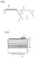
- FIG. 1is a schematic diagram to describe the formation of a (1-101) facet of a nitride semiconductor film.
- FIG. 2is a sectional view of a light emitting device according to an embodiment of the present invention.
- FIG. 3shows the relationship of the substrate nitride semiconductor film employed in the present invention.
- FIGS. 4-7Dare diagrams to describe a fabrication method of a compound semiconductor of the present invention.
- FIGS. 8A-8Dare diagrams to describe the crystal orientation relationship in an Si substrate according to a fifth embodiment.
- FIG. 9is a sectional view showing a semiconductor light emitting device of a sixth embodiment.
- FIG. 10is a sectional view of a semiconductor light emitting device of a seventh embodiment.
- FIG. 1is a schematic diagram to describe formation of a (1-101) facet 70 of a nitride semiconductor film of the present embodiment.
- FIG. 2is a schematic cross sectional view of a structure of the present nitride semiconductor light emitting device.
- a mask 52 of SiO 2is applied partially on a (001) Si off-oriented substrate 1 having a main plane inclined 7.3° to the [0-1-1] direction.
- the portion not masked with SiO 2 52is etched to form a trench having a (111) facet 61 in a relationship of 62 degrees from off oriented substrate (main plane) 60 .
- n-AlGaInN layer 10Upon facet 61 are sequentially stacked in a planarized manner an n-AlGaInN layer 10 , a first clad layer 2 formed of n-GaInN, a light emitting layer 3 formed of In x Ga 1 ⁇ x N, a carrier block layer 4 formed of p-AlGaInN, and a second clad layer 5 formed of p-GaInN. Furthermore, an electrode 15 is formed at the back side of silicon substrate 1 . A transparent electrode 16 is formed at a top plane of second clad layer 5 . A bonding electrode 17 is provided on a portion of transparent electrode 16 . In FIG. 2, the structure of SiO 2 mask 52 , the trench and the like are not depicted.
- the light emitting layer of In x Ga 1 ⁇ x Ncan emit light from ultraviolet to red in the wavelength by altering the composition x of In x Ga 1 ⁇ x N.
- the resistance of second clad layer 5 of the p conductivity type doped with magnesiumis high. Therefore, there is a possibility that the current density will not be uniform throughout light emitting layer 3 even if current, i.e., holes, are introduced to one end of second clad layer 5 from just bonding electrode 17 .
- a thin film transparent electrode 16is provided between electrode 17 and second clad layer 5 , substantially all over second clad layer 5 .
- Metalis to be employed for electrode 15 connected on the n conductivity type silicon substrate. It is desirable that this metal includes any of Al, Ti, Zr, Hf, V, and Nb. A metal of not more than 20 nm in thickness is to be employed for transparent electrode 16 connected to second clad layer 5 of the p conductivity type formed of GaN. It is desirable that this metal includes any of Ta, Co, Rh, Ni, Pd, Pt, Cu, Ag, Au.
- a method of the fabricating a light emitting device of the present embodimentwill be described with reference to FIG. 1 .
- a silicon oxide film or silicon nitride film 52On a rinsed silicon substrate is deposited a silicon oxide film or silicon nitride film 52 to a thickness of 100 nm by sputtering or CVD. Then, photolithography is applied to partially remove the silicon oxide film or silicon nitride film in stripes. The wafer is subjected to acid etching or the like by a buffered hydrofluoric acid to form a trench having an Si (111) facet 61 . The trench is provided in stripes extending in the Si [01-1] direction. As shown in FIG. 1, (111) facet 61 has a relationship of 62 degrees from main plane 60 of silicon substrate 1 due to the aforementioned plane orientation.
- This planecan be easily formed by appropriately adjusting the temperature of the acid etchant and the etching rate well known in the field of art. This plane can also be formed easily by using an alkaline etchant such as KOH.
- an alkaline etchantsuch as KOH.
- the remaining area not related to crystal growthis preferably masked with a material such as silicon nitride or silicon oxide that suppresses growth of the nitride semiconductor thereon.
- a nitride semiconductor filmis grown under the growth conditions set forth below on the substrate by MOCVD (metal organic chemical vapor deposition).
- MOCVDmetal organic chemical vapor deposition
- crystal growthproceeds with the axis perpendicular to facet plane 61 having a relationship of 62 degrees from the silicon substrate as the c axis of the nitride semiconductor film, as shown in FIG. 3.
- a nitride semiconductor filmis formed with the (1-101) facet as a plane 70 .
- the silicon substrate employed herehas a main plane 60 that is inclined 7.3° in the [0-1-1) direction from the (001) plane, i.e. rotated 7.3° about the [01-1] axis from the (001) plane, whereby plane 70 will have a plane orientation substantially identical to that of main plane 60 of the silicon substrate.
- An extremely planar GaN plane that substantially has a (1-101) planeis obtained even in the case of a plane inclined in the range of within 3 degrees from this plane in an arbitrary direction.
- a structurecan be provided wherein a nitride semiconductor film is grown only on the trench as shown in FIG. 1 to continuously form a light emitting device on (1-101) facet 70 of the nitride semiconductor film.
- a semiconductor light emitting devicecan be provided on the continuous film.
- an elementis formed on a continuous film obtained in this manner.
- a silicon substrate 1 having a trench formed by the above-described processis introduced into a MOCVD apparatus.
- a hydrogen (H 2 ) atmospherecleaning is effected at the high temperature of approximately 1100° C.
- TMATrimethyl gallium
- TMITrimethyl gallium
- SiH 4silane
- the trench portionis filled and adjacent first clad layers 2 of Ga 0.92 In 0.08 N are combined to form first clad layer 2 of Ga 0.92 In 0.08 N having a flat (1-101) plane 70 on the Si substrate.
- the growth temperature for first clad layer 2can be increased to result in a GaN film.
- growth at low temperatureis allowed without having to raise the growth temperature to a high temperature. By carrying out the growth at low temperature, there are fewer generations of cracks.
- TMATrimethyl indium
- TMITrimethyl indium
- TMGTrimethyl indium
- a well layer of In 0.18 Ga 0.82 Nis grown to the thickness of 3 nm.
- the temperatureis raised again up to 850° C., and TMG is introduced at 14 ⁇ mol/min. to grow a barrier layer of GaN.
- MQWmultiple quantum well
- TMG, TMA, TMI, and biscyclo pentadienyl magnesium (Cp 2 Mg) which is a p type doping source gasare introduced at 11 ⁇ mol/min., 1.1 ⁇ mol/min., 40 ⁇ mol/min. and 10 ⁇ mol/min., respectively, at a temperature identical to that of the last barrier layer to grow a p type carrier block layer 4 of Al 0.20 Ga 0.75 In 0.05 N to a thickness of 50 nm.
- p type carrier block layer 4of Al 0.20 Ga 0.75 In 0.05 N to a thickness of 50 nm.
- supply of TMAis stopped, and p type second clad layer 5 of Ga 0.9 In 0.1 N is grown to a thickness of 80 nm at the same growth temperature.
- the characteristics of the produced semiconductor devicewere measured.
- the active layer thereofexhibited extremely high planarity and variation in the layer thickness was small.
- a semiconductor light emitting device having a narrow half band width of 15 nm in the emission spectrumis obtained.
- the intensity of the emitted lightwas at least 10 times that of an element formed on a conventional Si (111) substrate.
- a light emitting device structureis formed directly on a silicon substrate inclined 7.3 degrees from the (001) plane.
- this off-oriented silicon substrateas an underlayer substrate to produce a GaN substrate and then removing the silicon, a planer GaN substrate can be obtained, which can be used for the production of a semiconductor device.
- GaNis grown with an AlN intermediate layer on the Si off-oriented substrate by MOCVD.
- This intermediate layermay be substituted with an intermediate layer of AlInN, AlGaN to obtain a similar result.
- This substrateis introduced into a HVPE (hydride VPE) apparatus.
- the temperature of the substrateis raised up to approximately 1050° C. while introducing N 2 carrier gas and NH 3 respectively at 5 l/min.
- GaClis introduced 100 cc/min. on the substrate to initiate growth of a GaN thick film.
- GaClis produced by conducting HCl gas to the Ga metal maintained at approximately 850° C.
- impuritiescan be doped arbitrarily during the growing step.
- monosilane (SiH 4 )is supplied 200 mol/min. (Si impurity concentration approximately 3.8 ⁇ 10 18 cm ⁇ 3 ) at the same time the growing step is initiated to form an Si doped GaN film.
- the above-described growing stepis carried out 8 hours to produce GaN having a total film thickness of approximately 350 ⁇ m on the Si substrate.
- the Si substrateis removed by grinding or etching to obtain an extremely planar GaN substrate having a (1-101) plane.
- a GaN substrate having a (1-101) plane at the surfacecan be obtained.
- This GaN substrateis rinsed and introduced in to a MOCVD equipment.
- the substrate temperatureis raised up to 760° C., and trimethyl indium (TMI) which is the indium source and TMG are introduced at 6.5 ⁇ mol/min. and 2.8 ⁇ mol/min. respectively, to form a well layer of In 0.18 Ga 0.72 N to a thickness of 3 nm on the GaN substrate.
- TMItrimethyl indium
- TMGis introduced 14 ⁇ mol/min. to grow a barrier layer of GaN.
- the growth of the well layer and barrier layeris repeated to form a light emitting layer 3 of a multiple quantum well (MQW) including 4 pairs.
- MQWmultiple quantum well
- TMG, TMA, TMI, and biscyclo pentadienyl magnesium (Cp 2 Mg) which is a p type doping source gasare introduced at 11 ⁇ mol/min., 1.1 ⁇ mol/min., 40 ⁇ mol/min. and 10 ⁇ mol/min. respectively, at a temperature identical to that of the last barrier layer to grow p type carrier block layer 4 of Al 0.20 Ga 0.75 In 0.05 N to a thickness of 50 nm.
- the supply of TMAis stopped, and p type second clad layer 50 of Ga 0.9 In 0.1 N is grown to a thickness of 80 nm at the same growth temperature.
- an extremely planer GaN substrateis produced having a (1-101) plane 70 .
- a semiconductor deviceusing this planar GaN substrate, a semiconductor light emitting device having a narrow half band width of 15 nm in the emission spectrum is obtained.
- the intensity of the emitted light of the obtained light emitting deviceis more than three times that of the device of the first embodiment.
- a light emitting device structurewas produced by vapor deposition employing organic metal on a silicon substrate inclined 7.3 degrees from the (001) plane.
- a light emitting devicecan be produced by a growth step using molecular beam epitaxy (MBE).
- MBEmolecular beam epitaxy
- the MOCVD growing step of the first embodimentis altered to the MBE growing step set forth below.
- the metals of Ga, Al, and Inare employed as the sources of Ga, Al, and In.
- a rinsed silicon substrate 1is introduced into a MBE equipment. Cleaning is effected at the high temperature of approximately 1100° C. in high vacuum.
- first clad layer 2 of silicon doped Ga 0.92 In 0.08 Nto a thickness of approximately 300 nm.
- metals Ga, Al and In, and MGwhich is the p type doping source gas are introduced at a temperature identical to that of the last barrier layer to grow a p type Al 0.20 Ga 0.75 In 0.05 N carrier block layer 4 to a thickness of 50 nm.
- MGwhich is the p type doping source gas
- transparent electrode 16is formed at the upper plane of the p type second clad layer of Ga 0.9 In 0.1 N.
- bonding electrode 17is formed at a portion of transparent electrode 16 .
- Electrode 15is formed at the bottom plane of the Si substrate.
- a trench slope inclined approximately 62 degrees from the silicon main planewas obtained taking advantage of the feature that the Si (111) plane is readily formed by etching (wet etching) using an etchant.
- the obtained slopeis the so-called crystal facet, stable in working accuracy as well as superior in planarity. It is favorable as an underlayer on which a nitride semiconductor is grown.
- the application range of the present inventionis not limited thereto.
- the inventorscarried out various experiments so as to form an inclined trench that is 62 degrees from the main plane, instead of using a silicon substrate inclined 7.3 degrees from the (001) plane as the main plane, by applying a mask 52 partially to another plane similar to the silicon plane in the first embodiment, and altering the etching temperature and rate.
- crystal growthcan be carried out so that the GaN (1-101) plane is substantially parallel to the substrate main plane.
- a continuous crystal film with a planar GaN (1-101) plane at the surfacecan be obtained.
- GaNis a crystal of potent orientation.
- the c axisis oriented perpendicular to the main plane. Therefore, the obtained crystal had the C plane as the main plane. It was conventionally difficult to obtain a crystal having a plane differing from the C plane.
- a crystal having a GaN (1-101) plane as the main planecan be easily obtained.
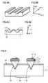
- a 100 nm-thick mask 52 of a silicon oxide film or silicon nitride film for facet formationis formed in the pattern of stripes extending in the Si [01-1] direction by means of film deposition such as sputtering and also photolithography on a silicon substrate inclined 7.3° in the [0-1-1] direction from the (001) plane.
- a trench having a (111) facet 61 as a slopeis formed by etching using a diluted KOH solution.
- the configuration of the trenchis V-shaped or a modification of the V-shape with a flat bottom region.
- One of the slopes of the trenchbecomes a (1-1-1) facet.
- the silicon substrateis an off-oriented substrate, the configuration of the V-shape is not symmetrical.
- the (111) planeis a plane inclined approximately 62° with respect to the substrate main plane whereas the (1-1-1) slope is a plane inclined approximately 47° with respect to the substrate main plane.
- the substrateis placed in the sputtering apparatus in an inclined state to grow a film with no film grown on (111) facet 61 .
- Mask 52 of a silicon oxide film or silicon nitride filmis applied so as to also cover the (1-1-1) facet, as shown in FIG. 6 .
- This structureis employed as the substrate for producing a nitride semiconductor film.
- FIGS. 8A-8Dshow the orientation relationship of the Si substrate, the facet, and the like.
- a growing step by MOCVDis applied on the processed Si substrate.
- An AlInN intermediate layeris grown on the Si off oriented substrate, followed by the growth of GaN.
- a continuous GaN substratecan be produced.
- Crystal growthstarts from the (111) facet (FIG. 8 A).
- the growing nitride semiconductorhas the ⁇ 0001> orientation located perpendicular to the slope.
- a GaN (1-101) planeappears substantially parallel to the substrate main plane. Therefore during the growth process, the crystal takes the shape of a triangular prism extending in the direction of the stripes (FIG. 7 B). The diameter of the triangular prism becomes larger as the growth proceeds.
- each separated crystal of the triangular prismcombine to result in a GaN crystal film having a planar GaN (1-101) plane at the surface (FIG. 7 D).
- the (111) facetis employed as a slope inclined 62° from the main plane using the above-described (001) plane off-oriented silicon substrate.
- an Si facet of (211)can be produced instead of (111).
- trenches in stripes extending in the [01-1] directionare produced to form a slope having a (211) facet inclined 62° from the main plane. This can be employed to obtain a GaN crystal film that has a similar flat surface.
- the nitride semiconductor crystalis grown with the perpendicular axis to the (211) facet as the c axis.
- an Si off-oriented substratethat is angled 62° from the (211) plane, a similar planar GaN substrate is obtained.
- the usage of an Si substratefacilitates crystal growth in the c axis orientation of the nitride semiconductor film with respect to the substrate.
- the usage of a substrate that is angled 62° of the facetallows the usage of a crystal film having the (1-101) facet of a planar nitride semiconductor.
- the light emitting layerhas the (1-101) plane as the main plane. This differs from the conventional case where the device formed using a sapphire substrate, a SiC substrate or a Si (111) substrate has (0001) as the main plane.
- a thin film with the (0001) of the nitride semiconductor which is a wurtzite structure as the main planeis equivalent in the band structure in the direction parallel to the main plane.
- a thin film that has the (1-101) plane as the main plane such as in the present inventionis not equivalent in the band structure even in the direction parallel to the main plane. Therefore, a light emitting device to which the present invention is applied has the degeneracy of the energy band resolved in the direction parallel to the light emitting layer (active layer). Therefore, high light emitting efficiency can be realized. Also, a significantly low threshold value can be realized in the application to a semiconductor laser device.
- a continuous nitride semiconductor filmwas formed through the growing process up to the step shown in FIG. 7D, and a semiconductor light emitting device was produced thereon.
- the crystal growth of each nitride semiconductor layeris ended at the process of FIG. 7B from the step of FIG. 7A, i.e., at the state where each crystal of the triangular prism shape do not combine with each other.
- a semiconductor light emitting deviceis formed separately at each crystal of the triangular prism to allow each light emitting device to emit radiation.
- the devicehas a multilayered structure of an n-AlGaInN intermediate layer 10 , an n-GaN underlying layer 11 , a first clad layer 2 of n-GaInN, a light emitting layer 3 of In x Ga 1 ⁇ x N, a carrier block layer 4 of p-AlGaInN, and a second clad layer 5 of p-GaInN sequentially stacked on facet 61 formed on the Si substrate.
- Electrode 15is provided at the bottom plane of the silicon substrate.
- a transparent electrode 16is provided at a top surface of second clad layer 5 .
- a bonding electrode 17is provided on a portion of transparent electrode 16 .
- the previous first to fourth embodimentsare based on a structure where a nitride semiconductor is grown only at one side slope of trenches provided in strips in an Si substrate.
- the slopes of both sidesare formed to have a predetermined off angle from the main plane.
- Each semiconductor light emitting deviceis formed at the Si slope of both sides in a manner similar to that of the sixth embodiment, as shown in FIG. 10 .
- the description of the above embodimentsis based on a semiconductor light emitting device which is an LED as the semiconductor device.
- the application of the present inventionis not limited to such a device, and can be applied to a semiconductor laser device.
- the present inventioncan also be applied to a GaN type MESFET having an electrode of a source, drain and gate formed at a film produced by growing an Si doped GaN layer via a high resistance layer of an AlGaN layer using the above-described method.
- the present inventionis further applicable to a GaN type MODFET that has the GaN channel layer subjected to Si modulation doping. Since the planarity of each layer can be improved therein, the abruptness of the channel layer interface can be increased to facilitate the mobility of electrons running in the channel layer by the uneven scattering. A semiconductor device of favorable electrical characteristics in the cutoff frequency can be obtained. Furthermore, since the conductivity between the Si substrate and the nitride semiconductor layer can be ensured, the device can be formed integrally on the Si substrate to allow fabrication of an integrated
- FIG. 2is a sectional view of a nitride semiconductor light emitting device of the eighth embodiment.
- the nitride semiconductor light emitting device of the present embodimenthas a multilayered structure of an n-AlGaInN layer 10 , a first clad layer 2 of n-GaInN, a light emitting layer 3 of Ga x In 1 ⁇ x N, a carrier block layer 4 of p-AlGaInN, and a second clad layer 5 of p-GaInN sequentially stacked on a silicon(112) substrate 1 .
- An electrode 15is provided at a bottom plane (back side) of silicon (112) plane substrate 1 .
- a transparent electrode 16is provided at the top surface of second clad layer 5 .
- a bonding electrode 17is provided on a portion of transparent electrode 16 .
- the wavelength of the bandis variable to emit light from ultraviolet to red in light emitting layer 3 .
- the present embodimentemploys a light emitting layer that emits light in blue.
- the value of xis 0.82.
- the resistance of p type second clad layer 5 doped with magnesiumis high. Therefore, there is a possibility that the current density may not be uniform throughout light emitting layer 3 even if current, i.e., holes, are injected from just bonding electrode 17 to one end of second clad layer 5 .
- a thin-film transparent electrode 16is provided between bonding electrode 17 and second clad layer 5 , all over the entire area of second clad layer 5 . Accordingly, more light can be output from this portion.
- Electrode 15 formed on n type silicon (112) plane substrate 1may include any metal of Al, Ti, Zr, Hf, V, and Nb. These metals are desirable from the standpoint of reducing contact resistance and driving voltage.
- metalsuch as any of Ta, Co, Rh, Ni, Pd, Pt, Cu, Ag, and Au or ITO and the like having a thickness of not more than 20 nm is preferably employed. Accordingly, the adherence is improved to allow reduction of the contact resistance and driving voltage.
- a method of fabricating a nitride semiconductor light emitting device of the present embodimentwill be described hereinafter.
- Silicon (112) plane substrate 1is rinsed and placed in a MOCVD. Cleaning is effected in a hydrogen (H 2 ) atmosphere at the high temperature of approximately 1100° C.
- the (112) planeis employed for the main plane of silicon substrate 1 . According to the experiment carried out by the inventors, a planer nitride semiconductor layer is obtained with respect to a plane inclined within the range of approximately ⁇ 5 degrees in all directions.
- TMAtrimethyl aluminium
- TMItrimethyl indium
- SiH 4 gasis introduced at 5 l/min., 10 ⁇ mol/min., 17 ⁇ mol/min., and 0.1 ⁇ mol/min., respectively, while introducing N 2 at 10 l/min. as carrier gas to form an Al 0.85 In 0.15 N layer 10 of approximately 10 nm in thickness.
- an AlInN intermediate layeris employed.
- a similar resultcan be obtained by using an intermediate layer of AlN, AlGaN, or AlGaInN.
- TMAtrimethyl gallium
- TMItrimethyl gallium
- SiH 4 gasare introduced at 20 ⁇ mol/min., 100 ⁇ mol/min., and 0.05 ⁇ mol/min., respectively, to grow a first clad layer 2 of silicon-doped Ga 0.92 In 0.08 N to a thickness of approximately 300 nm.
- the growth temperature for first clad layer 2can be increased to result in an GaN film.
- growth at low temperatureis allowed and generation of cracks can be suppressed.
- TMATrimethyl indium
- TMITrimethyl indium
- TMGTrimethyl indium
- the temperatureis raised again up to 850° C., and TMG is introduced at 14 ⁇ mol/min. to grow a barrier layer of GaN.
- TMGis introduced at 14 ⁇ mol/min. to grow a barrier layer of GaN.
- the growth of the well layer and the barrier layeris repeated to produce a light emitting layer 3 of a multiple quantum well (MQW) of 4 pairs.
- MQWmultiple quantum well
- TMG, TMA, TMI, and biscyclo pentadienyl magnesium (Cp 2 Mg) which is a p type doping source gasare introduced at 11 ⁇ mol/min., 1.1 ⁇ mol/min., 40 ⁇ mol/min. and 10 ⁇ mol/min., respectively, to grow a p type carrier block layer 4 of Al 0.20 Ga 0.75 In 0.05 N to a thickness of 50 nm at a temperature identical to that of the last barrier layer.
- p type second clad layer 5 of Ga 0.9 In 0.1 Nis grown to a thickness of 80 nm at the same growth temperature. This completes the growth of the light emitting device structure.
- supply of TMG, TMI and Cp 2 Mgis stopped and the temperature is lowered to room temperature.
- the light emitting device structureis output from the MOCVD apparatus.
- a transparent electrode 16is formed at the top surface of second clad layer 5 , and a bonding electrode 17 is formed on a portion of transparent electrode 16 .
- Electrode 15is formed at the bottom plane of silicon (112) plane substrate 1 .
- the characteristics of the above-produced semiconductor devicewere measured.
- the usage of a silicon (112) plane substrate 1allows the formation of a planer layer by the two dimensional growth due to the presence of many macrosteps at the silicon surface. Accordingly, the abruptness at the interface within the structure is increased to reduce the leakage current that thus not contribute to light emission.
- the semiconductor devicehas a light emission of 3.0 mW with the forward current of 20 mA, exhibiting light emission higher than that of a conventional semiconductor device.
- Silicon (112) plane substrate 1can be easily cut into the two directions of the axes of ⁇ 11-2> and ⁇ 1-10>. Therefore, a square LED chip can be fabricated, suppressed in chipping at the silicon end plane.
- a plane inclined 62 degrees from the main plane of a silicon substratea plane corresponding to a silicon substrate (001) plane rotated 7.3 degrees about the [01-1] axis, or a plane inclined at the range within 3 degrees in an arbitrary direction from these planes as to a nitride semiconductor device formed on a silicon substrate in the present invention
- an extremely planar crystal film of high quality with a (1-101) epitaxial planecan be obtained.
- this epitaxial planea semiconductor device having an abrupt interface and superior photoelectric characteristics can be provided.
- the silicon substrateSince a silicon substrate having la main plane formed of a plane in the range of ⁇ 5 degrees in an arbitrary direction from the (112) plane is employed, the silicon substrate can be easily cut in the two directions of the axes of ⁇ 11-2> and ⁇ 1-10>. Generation of chipping at the edge of a semiconductor device after being diced into chips can be suppressed effectively.
- a planer nitride semiconductor layercan be formed on the main plane of the silicon substrate, a semiconductor device that has a light emitting intensity higher then that of a conventional semiconductor device can be provided.
Landscapes
- Led Devices (AREA)
Abstract
Description
Claims (10)
Applications Claiming Priority (6)
| Application Number | Priority Date | Filing Date | Title |
|---|---|---|---|
| JP2000382164AJP2002185041A (en) | 2000-12-15 | 2000-12-15 | Semiconductor element |
| JP2000-382320 | 2000-12-15 | ||
| JP2000-382164 | 2000-12-15 | ||
| JP2000382320 | 2000-12-15 | ||
| JP2001-112821 | 2001-04-11 | ||
| JP2001112821AJP4743989B2 (en) | 2000-12-15 | 2001-04-11 | Semiconductor device, method for manufacturing the same, and method for manufacturing a semiconductor substrate |
Publications (2)
| Publication Number | Publication Date |
|---|---|
| US20020074561A1 US20020074561A1 (en) | 2002-06-20 |
| US6635901B2true US6635901B2 (en) | 2003-10-21 |
Family
ID=27345456
Family Applications (1)
| Application Number | Title | Priority Date | Filing Date |
|---|---|---|---|
| US10/021,677Expired - LifetimeUS6635901B2 (en) | 2000-12-15 | 2001-12-12 | Semiconductor device including an InGaAIN layer |
Country Status (1)
| Country | Link |
|---|---|
| US (1) | US6635901B2 (en) |
Cited By (46)
| Publication number | Priority date | Publication date | Assignee | Title |
|---|---|---|---|---|
| US20030031219A1 (en)* | 2001-08-08 | 2003-02-13 | Nobuhiko Sawaki | Semiconductor laser device and fabrication method thereof |
| US20030178702A1 (en)* | 2002-03-19 | 2003-09-25 | Nobuhiko Sawaki | Light emitting semiconductor device and method of fabricating the same |
| US20030198837A1 (en)* | 2002-04-15 | 2003-10-23 | Craven Michael D. | Non-polar a-plane gallium nitride thin films grown by metalorganic chemical vapor deposition |
| WO2004061969A1 (en)* | 2002-12-16 | 2004-07-22 | The Regents Of The University Of California | Growth of planar, non-polar a-plane gallium nitride by hydride vapor phase epitaxy |
| US20050045894A1 (en)* | 2000-12-15 | 2005-03-03 | Hiroyuki Okuyama | Semiconductor light emitting device and fabrication method thereof |
| US20050214992A1 (en)* | 2002-12-16 | 2005-09-29 | The Regents Of The University Of California | Fabrication of nonpolar indium gallium nitride thin films, heterostructures and devices by metalorganic chemical vapor deposition |
| US20050245095A1 (en)* | 2002-04-15 | 2005-11-03 | The Regents Of The University Of California | Growth of planar reduced dislocation density m-plane gallium nitride by hydride vapor phase epitaxy |
| US20050247952A1 (en)* | 2004-05-07 | 2005-11-10 | Pao-I Huang | Semiconductor light emitting device and method of making the same |
| US20060008941A1 (en)* | 2002-12-16 | 2006-01-12 | Basf Aktiengesellschaft | Growth of planar, non-polar a-plane gallium nitride by hydride vapor phase epitaxy |
| US20060270076A1 (en)* | 2005-05-31 | 2006-11-30 | The Regents Of The University Of California | Defect reduction of non-polar and semi-polar III-nitrides with sidewall lateral epitaxial overgrowth (SLEO) |
| US20070111488A1 (en)* | 2004-05-10 | 2007-05-17 | The Regents Of The University Of California | Fabrication of nonpolar indium gallium nitride thin films, heterostructures and devices by metalorganic chemical vapor deposition |
| US20070125996A1 (en)* | 2001-01-18 | 2007-06-07 | Sony Corporation | Crystal firm, crystal substrate, and semiconductor device |
| US20070184637A1 (en)* | 2004-06-03 | 2007-08-09 | The Regents Of The University Of California | Growth of planar reduced dislocation density m-plane gallium nitride by hydride vapor phase epitaxy |
| US20080113496A1 (en)* | 2006-11-15 | 2008-05-15 | The Regents Of The University Of California | METHOD FOR HETEROEPITAXIAL GROWTH OF HIGH-QUALITY N-FACE GaN, InN, AND AlN AND THEIR ALLOYS BY METAL ORGANIC CHEMICAL VAPOR DEPOSITION |
| US20080135853A1 (en)* | 2002-04-15 | 2008-06-12 | The Regents Of The University Of California | Dislocation reduction in non-polar iii-nitride thin films |
| US20080163814A1 (en)* | 2006-12-12 | 2008-07-10 | The Regents Of The University Of California | CRYSTAL GROWTH OF M-PLANE AND SEMIPOLAR PLANES OF (Al, In, Ga, B)N ON VARIOUS SUBSTRATES |
| US20080278646A1 (en)* | 2007-05-08 | 2008-11-13 | Chunghwa Picture Tubes, Ltd. | Pixel and driving method thereof for optically compensated bend mode liquid crystal display |
| CN100463240C (en)* | 2005-04-15 | 2009-02-18 | 晶能光电(江西)有限公司 | Method for preparing indium gallium aluminum nitrogen thin film and light-emitting device on silicon substrate |
| US20090159870A1 (en)* | 2007-12-20 | 2009-06-25 | Hung-Cheng Lin | Light emitting diode element and method for fabricating the same |
| US20090246944A1 (en)* | 2006-11-15 | 2009-10-01 | The Regents Of The University Of California | METHOD FOR HETEROEPITAXIAL GROWTH OF HIGH-QUALITY N-FACE GaN, InN, AND AlN AND THEIR ALLOYS BY METAL ORGANIC CHEMICAL VAPOR DEPOSITION |
| US20090298212A1 (en)* | 2007-06-12 | 2009-12-03 | Pan Shaoher X | Silicon Based Solid State Lighting |
| US20100032700A1 (en)* | 2008-08-11 | 2010-02-11 | Chen-Hua Yu | Light-Emitting Diodes on Concave Texture Substrate |
| US20100038655A1 (en)* | 2008-08-18 | 2010-02-18 | Ding-Yuan Chen | Reflective Layer for Light-Emitting Diodes |
| US20100127236A1 (en)* | 2008-11-21 | 2010-05-27 | Palo Alto Research Center Incorporated | Laser Diode With High Indium Active Layer And Lattice Matched Cladding Layer |
| US20100203662A1 (en)* | 2007-06-12 | 2010-08-12 | Siphoton, Inc | Light emitting device |
| US20100308300A1 (en)* | 2009-06-08 | 2010-12-09 | Siphoton, Inc. | Integrated circuit light emission device, module and fabrication process |
| US20110045658A1 (en)* | 2009-08-21 | 2011-02-24 | Hsueh-Hsing Liu | Method for fabricating a semi-polar nitride semiconductor |
| US20110108800A1 (en)* | 2008-06-24 | 2011-05-12 | Pan Shaoher X | Silicon based solid state lighting |
| US20110175055A1 (en)* | 2010-01-21 | 2011-07-21 | Pan Shaoher X | Solid state lighting device on a conductive substrate |
| US20110177636A1 (en)* | 2010-01-21 | 2011-07-21 | Pan Shaoher X | Manufacturing process for solid state lighting device on a conductive substrate |
| US20110210343A1 (en)* | 2010-03-01 | 2011-09-01 | Lextar Electronics Corporation | Semiconductor wafer |
| US20110306179A1 (en)* | 2010-06-11 | 2011-12-15 | Taiwan Semiconductor Manufacturing Company, Ltd. | MOCVD for Growing III-V Compound Semiconductors on Silicon Substrates |
| US20110304021A1 (en)* | 2010-06-11 | 2011-12-15 | Taiwan Semiconductor Manufacturing Company, Ltd. | Epitaxial Growth of III-V Compound Semiconductors on Silicon Surfaces |
| US20120094467A1 (en)* | 2010-10-19 | 2012-04-19 | Taiwan Semiconductor Manufacturing Company, Ltd. | Semiconductor device and manufacturing method with improved epitaxial quality of iii-v compound on silicon surfaces |
| US8217418B1 (en) | 2011-02-14 | 2012-07-10 | Siphoton Inc. | Semi-polar semiconductor light emission devices |
| US8372671B2 (en) | 2010-06-21 | 2013-02-12 | Micron Technology, Inc. | Solid state devices with semi-polar facets and associated methods of manufacturing |
| US20130069107A1 (en)* | 2010-05-20 | 2013-03-21 | Panasonic Corporation | Nitride semiconductor light emitting device and method of manufacturing the same |
| US8624292B2 (en) | 2011-02-14 | 2014-01-07 | Siphoton Inc. | Non-polar semiconductor light emission devices |
| US8722441B2 (en) | 2010-01-21 | 2014-05-13 | Siphoton Inc. | Manufacturing process for solid state lighting device on a conductive substrate |
| US20150069322A1 (en)* | 2013-04-12 | 2015-03-12 | Justin PAYNE | Semipolar emitter |
| CN104538282A (en)* | 2014-12-17 | 2015-04-22 | 江苏能华微电子科技发展有限公司 | Growing method of vertical structure power device epitaxial layer and power device |
| US20160343905A1 (en)* | 2001-07-24 | 2016-11-24 | Nichia Corporation | Semiconductor light emitting device |
| US10290497B2 (en)* | 2014-06-09 | 2019-05-14 | Seren Photonics Limited | Fabrication of semi-polar crystal structures |
| US20190229293A1 (en)* | 2014-10-09 | 2019-07-25 | Sony Corporation | Display unit, method of manufacturing display unit, and electronic apparatus |
| US20190334069A1 (en)* | 2012-11-02 | 2019-10-31 | Epistar Corporation | Light emitting device |
| US11342179B2 (en) | 2019-05-21 | 2022-05-24 | National Chiao Tung University | Semiconductor structure having a Si substrate heterointegrated with GaN and method for fabricating the same |
Families Citing this family (17)
| Publication number | Priority date | Publication date | Assignee | Title |
|---|---|---|---|---|
| TW517403B (en)* | 2002-01-10 | 2003-01-11 | Epitech Technology Corp | Nitride light emitting diode and manufacturing method for the same |
| JP3843245B2 (en)* | 2002-06-26 | 2006-11-08 | 宣彦 澤木 | Semiconductor light emitting element and semiconductor light emitting device |
| US7002182B2 (en)* | 2002-09-06 | 2006-02-21 | Sony Corporation | Semiconductor light emitting device integral type semiconductor light emitting unit image display unit and illuminating unit |
| JP2006179511A (en)* | 2004-12-20 | 2006-07-06 | Sumitomo Electric Ind Ltd | Light emitting device |
| TWI453813B (en)* | 2005-03-10 | 2014-09-21 | Univ California | Technology for growing flat semipolar gallium nitride |
| TWI455181B (en)* | 2005-06-01 | 2014-10-01 | Univ California | Growth and manufacturing techniques for semi-polar (Ga, Al, In, B) N films, heterostructures and devices |
| US8013320B2 (en)* | 2006-03-03 | 2011-09-06 | Panasonic Corporation | Nitride semiconductor device and method for fabricating the same |
| TWI482204B (en) | 2007-11-27 | 2015-04-21 | Sophia School Corp | Method for producing group III nitride structure and group III nitride structure |
| JP2010263189A (en)* | 2009-04-07 | 2010-11-18 | Sharp Corp | Nitride semiconductor light emitting diode |
| JP5446622B2 (en)* | 2009-06-29 | 2014-03-19 | 住友電気工業株式会社 | Group III nitride crystal and method for producing the same |
| US8350273B2 (en)* | 2009-08-31 | 2013-01-08 | Infineon Technologies Ag | Semiconductor structure and a method of forming the same |
| KR101315473B1 (en)* | 2009-12-07 | 2013-10-04 | 성균관대학교산학협력단 | transferred thin film transistor and method for manufacturing at the same |
| JP2013542599A (en)* | 2010-09-30 | 2013-11-21 | フリースケール セミコンダクター インコーポレイテッド | Method for processing a semiconductor wafer, semiconductor wafer and semiconductor device |
| US20130087763A1 (en)* | 2011-10-06 | 2013-04-11 | Electronics And Telecommunications Research Institute | Light emitting diode and method of manufacturing the same |
| KR102061696B1 (en)* | 2013-11-05 | 2020-01-03 | 삼성전자주식회사 | Semipolar nitride semiconductor structure and method of fabricating the same |
| CN103730479A (en)* | 2013-11-29 | 2014-04-16 | 南京大学扬州光电研究院 | GaN-based LED integrated chip with multiple light-emitting sub areas |
| US10818778B2 (en) | 2017-11-27 | 2020-10-27 | Taiwan Semiconductor Manufacturing Co., Ltd. | Heterogeneous semiconductor device substrates with high quality epitaxy |
Citations (6)
| Publication number | Priority date | Publication date | Assignee | Title |
|---|---|---|---|---|
| JPH05343741A (en) | 1991-12-18 | 1993-12-24 | Hiroshi Amano | Gallium nitride-based semiconductor device and manufacturing method thereof |
| JPH0864901A (en) | 1994-08-24 | 1996-03-08 | Hitachi Ltd | Structure of semiconductor laser diode |
| JPH10312971A (en) | 1997-03-13 | 1998-11-24 | Nec Corp | III-V compound semiconductor film and its growth method, GaN-based semiconductor film and its formation method, GaN-based semiconductor laminated structure and its formation method, GaN-based semiconductor element and its production method |
| US5945352A (en)* | 1997-12-19 | 1999-08-31 | Advanced Micro Devices | Method for fabrication of shallow isolation trenches with sloped wall profiles |
| US6304587B1 (en)* | 1999-06-14 | 2001-10-16 | Corning Incorporated | Buried ridge semiconductor laser with aluminum-free confinement layer |
| US6391784B1 (en)* | 1999-07-21 | 2002-05-21 | Advanced Micro Devices, Inc. | Spacer-assisted ultranarrow shallow trench isolation formation |
- 2001
- 2001-12-12USUS10/021,677patent/US6635901B2/ennot_activeExpired - Lifetime
Patent Citations (6)
| Publication number | Priority date | Publication date | Assignee | Title |
|---|---|---|---|---|
| JPH05343741A (en) | 1991-12-18 | 1993-12-24 | Hiroshi Amano | Gallium nitride-based semiconductor device and manufacturing method thereof |
| JPH0864901A (en) | 1994-08-24 | 1996-03-08 | Hitachi Ltd | Structure of semiconductor laser diode |
| JPH10312971A (en) | 1997-03-13 | 1998-11-24 | Nec Corp | III-V compound semiconductor film and its growth method, GaN-based semiconductor film and its formation method, GaN-based semiconductor laminated structure and its formation method, GaN-based semiconductor element and its production method |
| US5945352A (en)* | 1997-12-19 | 1999-08-31 | Advanced Micro Devices | Method for fabrication of shallow isolation trenches with sloped wall profiles |
| US6304587B1 (en)* | 1999-06-14 | 2001-10-16 | Corning Incorporated | Buried ridge semiconductor laser with aluminum-free confinement layer |
| US6391784B1 (en)* | 1999-07-21 | 2002-05-21 | Advanced Micro Devices, Inc. | Spacer-assisted ultranarrow shallow trench isolation formation |
Cited By (118)
| Publication number | Priority date | Publication date | Assignee | Title |
|---|---|---|---|---|
| US20050045894A1 (en)* | 2000-12-15 | 2005-03-03 | Hiroyuki Okuyama | Semiconductor light emitting device and fabrication method thereof |
| US7030421B2 (en)* | 2000-12-15 | 2006-04-18 | Sony Corporation | Semiconductor light emitting device and fabrication method thereof |
| US20070125996A1 (en)* | 2001-01-18 | 2007-06-07 | Sony Corporation | Crystal firm, crystal substrate, and semiconductor device |
| US7727331B2 (en)* | 2001-01-18 | 2010-06-01 | Sony Corporation | Crystal firm, crystal substrate, and semiconductor device |
| US20160343905A1 (en)* | 2001-07-24 | 2016-11-24 | Nichia Corporation | Semiconductor light emitting device |
| US9865773B2 (en)* | 2001-07-24 | 2018-01-09 | Nichia Corporation | Semiconductor light emitting device |
| US10593833B2 (en) | 2001-07-24 | 2020-03-17 | Nichia Corporation | Semiconductor light emitting device |
| US10396242B2 (en) | 2001-07-24 | 2019-08-27 | Nichia Corporation | Semiconductor light emitting device |
| US6888867B2 (en)* | 2001-08-08 | 2005-05-03 | Nobuhiko Sawaki | Semiconductor laser device and fabrication method thereof |
| US20030031219A1 (en)* | 2001-08-08 | 2003-02-13 | Nobuhiko Sawaki | Semiconductor laser device and fabrication method thereof |
| US20030178702A1 (en)* | 2002-03-19 | 2003-09-25 | Nobuhiko Sawaki | Light emitting semiconductor device and method of fabricating the same |
| US6844572B2 (en)* | 2002-03-19 | 2005-01-18 | Sharp Kabushiki Kaisha | Light emitting semiconductor device and method of fabricating the same |
| US20110229639A1 (en)* | 2002-04-15 | 2011-09-22 | The Regents Of The University Of California | Non-polar gallium nitride thin films grown by metalorganic chemical vapor deposition |
| US20110204329A1 (en)* | 2002-04-15 | 2011-08-25 | The Regents Of The University Of California | NON-POLAR (Al,B,In,Ga)N QUANTUM WELL AND HETEROSTRUCTURE MATERIALS AND DEVICES |
| US7091514B2 (en) | 2002-04-15 | 2006-08-15 | The Regents Of The University Of California | Non-polar (Al,B,In,Ga)N quantum well and heterostructure materials and devices |
| US9039834B2 (en) | 2002-04-15 | 2015-05-26 | The Regents Of The University Of California | Non-polar gallium nitride thin films grown by metalorganic chemical vapor deposition |
| US7982208B2 (en) | 2002-04-15 | 2011-07-19 | The Regents Of The University Of California | Non-polar (Al,B,In,Ga)N quantum well and heterostructure materials and devices |
| US20060278865A1 (en)* | 2002-04-15 | 2006-12-14 | Craven Michael D | Non-polar (Al,B,In,Ga)N quantum well and heterostructure materials and devices |
| US20080135853A1 (en)* | 2002-04-15 | 2008-06-12 | The Regents Of The University Of California | Dislocation reduction in non-polar iii-nitride thin films |
| US7208393B2 (en) | 2002-04-15 | 2007-04-24 | The Regents Of The University Of California | Growth of planar reduced dislocation density m-plane gallium nitride by hydride vapor phase epitaxy |
| US8188458B2 (en) | 2002-04-15 | 2012-05-29 | The Regents Of The University Of California | Non-polar (Al,B,In,Ga)N quantum well and heterostructure materials and devices |
| US20030198837A1 (en)* | 2002-04-15 | 2003-10-23 | Craven Michael D. | Non-polar a-plane gallium nitride thin films grown by metalorganic chemical vapor deposition |
| US20050245095A1 (en)* | 2002-04-15 | 2005-11-03 | The Regents Of The University Of California | Growth of planar reduced dislocation density m-plane gallium nitride by hydride vapor phase epitaxy |
| US8809867B2 (en) | 2002-04-15 | 2014-08-19 | The Regents Of The University Of California | Dislocation reduction in non-polar III-nitride thin films |
| US6900070B2 (en) | 2002-04-15 | 2005-05-31 | The Regents Of The University Of California | Dislocation reduction in non-polar gallium nitride thin films |
| US7186302B2 (en) | 2002-12-16 | 2007-03-06 | The Regents Of The University Of California | Fabrication of nonpolar indium gallium nitride thin films, heterostructures and devices by metalorganic chemical vapor deposition |
| US20060008941A1 (en)* | 2002-12-16 | 2006-01-12 | Basf Aktiengesellschaft | Growth of planar, non-polar a-plane gallium nitride by hydride vapor phase epitaxy |
| US7847293B2 (en) | 2002-12-16 | 2010-12-07 | The Regents Of The University Of California | Growth of reduced dislocation density non-polar gallium nitride |
| US8450192B2 (en) | 2002-12-16 | 2013-05-28 | The Regents Of The University Of California | Growth of planar, non-polar, group-III nitride films |
| US7220658B2 (en) | 2002-12-16 | 2007-05-22 | The Regents Of The University Of California | Growth of reduced dislocation density non-polar gallium nitride by hydride vapor phase epitaxy |
| US7427555B2 (en) | 2002-12-16 | 2008-09-23 | The Regents Of The University Of California | Growth of planar, non-polar gallium nitride by hydride vapor phase epitaxy |
| WO2004061969A1 (en)* | 2002-12-16 | 2004-07-22 | The Regents Of The University Of California | Growth of planar, non-polar a-plane gallium nitride by hydride vapor phase epitaxy |
| US20090001519A1 (en)* | 2002-12-16 | 2009-01-01 | The Regents Of The University Of California | Growth of planar, non-polar, group-iii nitride films |
| US20070126023A1 (en)* | 2002-12-16 | 2007-06-07 | The Regents Of The University Of California | Growth of reduced dislocation density non-polar gallium nitride |
| US20060128124A1 (en)* | 2002-12-16 | 2006-06-15 | Haskell Benjamin A | Growth of reduced dislocation density non-polar gallium nitride by hydride vapor phase epitaxy |
| US20050214992A1 (en)* | 2002-12-16 | 2005-09-29 | The Regents Of The University Of California | Fabrication of nonpolar indium gallium nitride thin films, heterostructures and devices by metalorganic chemical vapor deposition |
| US7141830B2 (en)* | 2004-05-07 | 2006-11-28 | Mediatek, Incorporated | Semiconductor light emitting device and method of making the same |
| US20050247952A1 (en)* | 2004-05-07 | 2005-11-10 | Pao-I Huang | Semiconductor light emitting device and method of making the same |
| US20070111488A1 (en)* | 2004-05-10 | 2007-05-17 | The Regents Of The University Of California | Fabrication of nonpolar indium gallium nitride thin films, heterostructures and devices by metalorganic chemical vapor deposition |
| US7504274B2 (en) | 2004-05-10 | 2009-03-17 | The Regents Of The University Of California | Fabrication of nonpolar indium gallium nitride thin films, heterostructures and devices by metalorganic chemical vapor deposition |
| US8882935B2 (en) | 2004-05-10 | 2014-11-11 | The Regents Of The University Of California | Fabrication of nonpolar indium gallium nitride thin films, heterostructures, and devices by metalorganic chemical vapor deposition |
| US8502246B2 (en) | 2004-05-10 | 2013-08-06 | The Regents Of The University Of California | Fabrication of nonpolar indium gallium nitride thin films, heterostructures and devices by metalorganic chemical vapor deposition |
| US20070184637A1 (en)* | 2004-06-03 | 2007-08-09 | The Regents Of The University Of California | Growth of planar reduced dislocation density m-plane gallium nitride by hydride vapor phase epitaxy |
| US20110193094A1 (en)* | 2004-06-03 | 2011-08-11 | The Regents Of The University Of California | Growth of planar reduced dislocation density m-plane gallium nitride by hydride vapor phase epitaxy |
| US7956360B2 (en) | 2004-06-03 | 2011-06-07 | The Regents Of The University Of California | Growth of planar reduced dislocation density M-plane gallium nitride by hydride vapor phase epitaxy |
| CN100463240C (en)* | 2005-04-15 | 2009-02-18 | 晶能光电(江西)有限公司 | Method for preparing indium gallium aluminum nitrogen thin film and light-emitting device on silicon substrate |
| US20080185690A1 (en)* | 2005-05-31 | 2008-08-07 | The Regents Of The University Of California | Defect reduction of non-polar and semi-polar iii-nitrides with sidewall lateral epitaxial overgrowth (sleo) |
| US7361576B2 (en) | 2005-05-31 | 2008-04-22 | The Regents Of The University Of California | Defect reduction of non-polar and semi-polar III-Nitrides with sidewall lateral epitaxial overgrowth (SLEO) |
| US20060270076A1 (en)* | 2005-05-31 | 2006-11-30 | The Regents Of The University Of California | Defect reduction of non-polar and semi-polar III-nitrides with sidewall lateral epitaxial overgrowth (SLEO) |
| US7955983B2 (en) | 2005-05-31 | 2011-06-07 | The Regents Of The University Of California | Defect reduction of non-polar and semi-polar III-nitrides with sidewall lateral epitaxial overgrowth (SLEO) |
| US7566580B2 (en) | 2006-11-15 | 2009-07-28 | The Regents Of The University Of California | Method for heteroepitaxial growth of high-quality N-face GaN, InN, and AIN and their alloys by metal organic chemical vapor deposition |
| US20090246944A1 (en)* | 2006-11-15 | 2009-10-01 | The Regents Of The University Of California | METHOD FOR HETEROEPITAXIAL GROWTH OF HIGH-QUALITY N-FACE GaN, InN, AND AlN AND THEIR ALLOYS BY METAL ORGANIC CHEMICAL VAPOR DEPOSITION |
| US8455885B2 (en) | 2006-11-15 | 2013-06-04 | The Regents Of The University Of California | Method for heteroepitaxial growth of high-quality N-face gallium nitride, indium nitride, and aluminum nitride and their alloys by metal organic chemical vapor deposition |
| US8193020B2 (en) | 2006-11-15 | 2012-06-05 | The Regents Of The University Of California | Method for heteroepitaxial growth of high-quality N-face GaN, InN, and AlN and their alloys by metal organic chemical vapor deposition |
| US20080113496A1 (en)* | 2006-11-15 | 2008-05-15 | The Regents Of The University Of California | METHOD FOR HETEROEPITAXIAL GROWTH OF HIGH-QUALITY N-FACE GaN, InN, AND AlN AND THEIR ALLOYS BY METAL ORGANIC CHEMICAL VAPOR DEPOSITION |
| US20080163814A1 (en)* | 2006-12-12 | 2008-07-10 | The Regents Of The University Of California | CRYSTAL GROWTH OF M-PLANE AND SEMIPOLAR PLANES OF (Al, In, Ga, B)N ON VARIOUS SUBSTRATES |
| US20080278646A1 (en)* | 2007-05-08 | 2008-11-13 | Chunghwa Picture Tubes, Ltd. | Pixel and driving method thereof for optically compensated bend mode liquid crystal display |
| US20100203662A1 (en)* | 2007-06-12 | 2010-08-12 | Siphoton, Inc | Light emitting device |
| US20090298212A1 (en)* | 2007-06-12 | 2009-12-03 | Pan Shaoher X | Silicon Based Solid State Lighting |
| US8313963B2 (en) | 2007-06-12 | 2012-11-20 | Siphoton Inc. | Light emitting device |
| US8268648B2 (en) | 2007-06-12 | 2012-09-18 | Siphoton Inc. | Silicon based solid state lighting |
| US8304794B2 (en) | 2007-06-12 | 2012-11-06 | Siphoton Inc. | Light emitting device |
| US8101447B2 (en)* | 2007-12-20 | 2012-01-24 | Tekcore Co., Ltd. | Light emitting diode element and method for fabricating the same |
| US20090159870A1 (en)* | 2007-12-20 | 2009-06-25 | Hung-Cheng Lin | Light emitting diode element and method for fabricating the same |
| US20110108800A1 (en)* | 2008-06-24 | 2011-05-12 | Pan Shaoher X | Silicon based solid state lighting |
| US20100032700A1 (en)* | 2008-08-11 | 2010-02-11 | Chen-Hua Yu | Light-Emitting Diodes on Concave Texture Substrate |
| US8134163B2 (en)* | 2008-08-11 | 2012-03-13 | Taiwan Semiconductor Manfacturing Co., Ltd. | Light-emitting diodes on concave texture substrate |
| US8629465B2 (en) | 2008-08-11 | 2014-01-14 | Taiwan Semiconductor Manufacturing Company, Ltd. | Light-emitting diodes on concave texture substrate |
| US9373755B2 (en) | 2008-08-11 | 2016-06-21 | Epistar Corporation | Light-emitting diodes on concave texture substrate |
| US20140235001A1 (en)* | 2008-08-18 | 2014-08-21 | Tsmc Solid State Lighting Ltd. | Reflective Layer for Light-Emitting Diodes |
| US8716723B2 (en)* | 2008-08-18 | 2014-05-06 | Tsmc Solid State Lighting Ltd. | Reflective layer between light-emitting diodes |
| US20160064632A1 (en)* | 2008-08-18 | 2016-03-03 | Epistar Corporation | Light-emitting device |
| US20100038655A1 (en)* | 2008-08-18 | 2010-02-18 | Ding-Yuan Chen | Reflective Layer for Light-Emitting Diodes |
| US9214613B2 (en)* | 2008-08-18 | 2015-12-15 | Tsmc Solid State Lighting Ltd. | Method of forming light-generating device including reflective layer |
| US10411177B2 (en)* | 2008-08-18 | 2019-09-10 | Epistar Corporation | Light emitting device |
| US10062821B2 (en) | 2008-08-18 | 2018-08-28 | Epistar Corporation | Light-emitting device |
| US10038129B2 (en)* | 2008-08-18 | 2018-07-31 | Epistar Corporation | Light emitting device |
| US9698325B2 (en)* | 2008-08-18 | 2017-07-04 | Epistar Corporation | Light-emitting device including reflective layer |
| US9893257B2 (en) | 2008-08-18 | 2018-02-13 | Epistar Corporation | Electrode structure of light emitting device |
| US9530948B2 (en)* | 2008-08-18 | 2016-12-27 | Epistar Corporation | Light emitting device having multi-layered electrode structure |
| US20100127236A1 (en)* | 2008-11-21 | 2010-05-27 | Palo Alto Research Center Incorporated | Laser Diode With High Indium Active Layer And Lattice Matched Cladding Layer |
| US8000366B2 (en)* | 2008-11-21 | 2011-08-16 | Palo Alto Research Center Incorporated | Laser diode with high indium active layer and lattice matched cladding layer |
| US20100308300A1 (en)* | 2009-06-08 | 2010-12-09 | Siphoton, Inc. | Integrated circuit light emission device, module and fabrication process |
| US20110045658A1 (en)* | 2009-08-21 | 2011-02-24 | Hsueh-Hsing Liu | Method for fabricating a semi-polar nitride semiconductor |
| US20110177636A1 (en)* | 2010-01-21 | 2011-07-21 | Pan Shaoher X | Manufacturing process for solid state lighting device on a conductive substrate |
| US8722441B2 (en) | 2010-01-21 | 2014-05-13 | Siphoton Inc. | Manufacturing process for solid state lighting device on a conductive substrate |
| US8674383B2 (en) | 2010-01-21 | 2014-03-18 | Siphoton Inc. | Solid state lighting device on a conductive substrate |
| US20110175055A1 (en)* | 2010-01-21 | 2011-07-21 | Pan Shaoher X | Solid state lighting device on a conductive substrate |
| US8283676B2 (en) | 2010-01-21 | 2012-10-09 | Siphoton Inc. | Manufacturing process for solid state lighting device on a conductive substrate |
| US20110210343A1 (en)* | 2010-03-01 | 2011-09-01 | Lextar Electronics Corporation | Semiconductor wafer |
| US9006778B2 (en)* | 2010-05-20 | 2015-04-14 | Panasonic Intellectual Property Mangement Co., Ltd. | Nitride semiconductor light emitting device and method of manufacturing the same |
| US20130069107A1 (en)* | 2010-05-20 | 2013-03-21 | Panasonic Corporation | Nitride semiconductor light emitting device and method of manufacturing the same |
| US8609517B2 (en)* | 2010-06-11 | 2013-12-17 | Taiwan Semiconductor Manufacturing Company, Ltd. | MOCVD for growing III-V compound semiconductors on silicon substrates |
| US8242540B2 (en)* | 2010-06-11 | 2012-08-14 | Taiwan Semiconductor Manufacturing Company, Ltd. | Epitaxial growth of III-V compound semiconductors on silicon surfaces |
| US20110304021A1 (en)* | 2010-06-11 | 2011-12-15 | Taiwan Semiconductor Manufacturing Company, Ltd. | Epitaxial Growth of III-V Compound Semiconductors on Silicon Surfaces |
| US20110306179A1 (en)* | 2010-06-11 | 2011-12-15 | Taiwan Semiconductor Manufacturing Company, Ltd. | MOCVD for Growing III-V Compound Semiconductors on Silicon Substrates |
| US8698173B2 (en) | 2010-06-21 | 2014-04-15 | Micron Technology, Inc. | Solid state lighting devices with semi-polar facets and associated methods of manufacturing |
| US8372671B2 (en) | 2010-06-21 | 2013-02-12 | Micron Technology, Inc. | Solid state devices with semi-polar facets and associated methods of manufacturing |
| US20120094467A1 (en)* | 2010-10-19 | 2012-04-19 | Taiwan Semiconductor Manufacturing Company, Ltd. | Semiconductor device and manufacturing method with improved epitaxial quality of iii-v compound on silicon surfaces |
| US8183134B2 (en)* | 2010-10-19 | 2012-05-22 | Taiwan Semiconductor Manufacturing Company, Ltd. | Semiconductor device and manufacturing method with improved epitaxial quality of III-V compound on silicon surfaces |
| US8426890B2 (en) | 2010-10-19 | 2013-04-23 | Taiwan Semiconductor Manufacturing Company, Ltd. | Semiconductor device and manufacturing method with improved epitaxial quality of III-V compound on silicon surfaces |
| US8624292B2 (en) | 2011-02-14 | 2014-01-07 | Siphoton Inc. | Non-polar semiconductor light emission devices |
| US8217418B1 (en) | 2011-02-14 | 2012-07-10 | Siphoton Inc. | Semi-polar semiconductor light emission devices |
| US10847682B2 (en)* | 2012-11-02 | 2020-11-24 | Epistar Corporation | Electrode structure of light emitting device |
| US11677046B2 (en)* | 2012-11-02 | 2023-06-13 | Epistar Corporation | Electrode structure of light emitting device |
| US20220376143A1 (en)* | 2012-11-02 | 2022-11-24 | Epistar Corporation | Electrode structure of light emitting device |
| US20190334069A1 (en)* | 2012-11-02 | 2019-10-31 | Epistar Corporation | Light emitting device |
| US11437547B2 (en)* | 2012-11-02 | 2022-09-06 | Epistar Corporation | Electrode structure of light emitting device |
| US20150069322A1 (en)* | 2013-04-12 | 2015-03-12 | Justin PAYNE | Semipolar emitter |
| US10290497B2 (en)* | 2014-06-09 | 2019-05-14 | Seren Photonics Limited | Fabrication of semi-polar crystal structures |
| US10826023B2 (en) | 2014-10-09 | 2020-11-03 | Sony Corporation | Display unit with disconnected organic layer at projected portion |
| US10497903B2 (en)* | 2014-10-09 | 2019-12-03 | Sony Corporation | Display unit, method of manufacturing display unit, and electronic apparatus for enhancement of luminance |
| US20190229293A1 (en)* | 2014-10-09 | 2019-07-25 | Sony Corporation | Display unit, method of manufacturing display unit, and electronic apparatus |
| US11563198B2 (en) | 2014-10-09 | 2023-01-24 | Sony Corporation | Display unit with organic layer disposed on metal layer and insulation layer |
| US11871611B2 (en) | 2014-10-09 | 2024-01-09 | Sony Corporation | Display unit with reflector layer and electronic apparatus |
| US12268049B2 (en) | 2014-10-09 | 2025-04-01 | Sony Corporation | Display unit with organic layer |
| CN104538282A (en)* | 2014-12-17 | 2015-04-22 | 江苏能华微电子科技发展有限公司 | Growing method of vertical structure power device epitaxial layer and power device |
| US11342179B2 (en) | 2019-05-21 | 2022-05-24 | National Chiao Tung University | Semiconductor structure having a Si substrate heterointegrated with GaN and method for fabricating the same |
Also Published As
| Publication number | Publication date |
|---|---|
| US20020074561A1 (en) | 2002-06-20 |
Similar Documents
| Publication | Publication Date | Title |
|---|---|---|
| US6635901B2 (en) | Semiconductor device including an InGaAIN layer | |
| US6841410B2 (en) | Method for forming group-III nitride semiconductor layer and group-III nitride semiconductor device | |
| US8492186B2 (en) | Method for producing group III nitride semiconductor layer, group III nitride semiconductor light-emitting device, and lamp | |
| US6844572B2 (en) | Light emitting semiconductor device and method of fabricating the same | |
| US6020602A (en) | GaN based optoelectronic device and method for manufacturing the same | |
| US6617182B2 (en) | Semiconductor device and semiconductor substrate, and method for fabricating the same | |
| US6380051B1 (en) | Layered structure including a nitride compound semiconductor film and method for making the same | |
| US6441403B1 (en) | Semiconductor device with roughened surface increasing external quantum efficiency | |
| US6455877B1 (en) | III-N compound semiconductor device | |
| US7943494B2 (en) | Method for blocking dislocation propagation of semiconductor | |
| US20140127848A1 (en) | Nitride semiconductor light-emittting device and process for producing the same | |
| US20050145865A1 (en) | Semiconductor light emitting element and method for manufacturing same, integrated semiconductor light-emitting device and method for manufacturing same, image display and method for manufacturing same, and illuminating device and method for manufacturing same | |
| JP3712770B2 (en) | Method for manufacturing group 3 nitride semiconductor and semiconductor device | |
| JPWO2009154215A1 (en) | Group III nitride semiconductor light emitting device, method for manufacturing the same, and lamp | |
| US6888867B2 (en) | Semiconductor laser device and fabrication method thereof | |
| JP2003152220A (en) | Semiconductor light emitting device manufacturing method and semiconductor light emitting device | |
| JP2001135892A (en) | Nitride semiconductor light emitting device | |
| JP3733008B2 (en) | III-N compound semiconductor device | |
| JP2010538491A (en) | Semiconductor light emitting device and manufacturing method thereof | |
| JP3545197B2 (en) | Semiconductor device and method of manufacturing the same | |
| WO2009142265A1 (en) | Iii nitride semiconductor light emitting element and method for manufacturing the same, and lamp | |
| JP4424840B2 (en) | III-N compound semiconductor device | |
| JP4058595B2 (en) | Semiconductor light emitting device and manufacturing method thereof | |
| JP4743989B2 (en) | Semiconductor device, method for manufacturing the same, and method for manufacturing a semiconductor substrate | |
| JP3718329B2 (en) | GaN compound semiconductor light emitting device |
Legal Events
| Date | Code | Title | Description |
|---|---|---|---|
| AS | Assignment | Owner name:SAWAKI, NOBUHIKO, JAPAN Free format text:ASSIGNMENT OF ASSIGNORS INTEREST;ASSIGNORS:SAWAKI, NOBUHIKO;HONDA, YOSHIO;KOIDE, NORIKATSU;AND OTHERS;REEL/FRAME:012389/0043 Effective date:20011130 Owner name:SHARP KABUSHIKI KAISHA, JAPAN Free format text:ASSIGNMENT OF ASSIGNORS INTEREST;ASSIGNORS:SAWAKI, NOBUHIKO;HONDA, YOSHIO;KOIDE, NORIKATSU;AND OTHERS;REEL/FRAME:012389/0043 Effective date:20011130 | |
| AS | Assignment | Owner name:SAWAKI, NOBUHIKO, JAPAN Free format text:CORRECTIVE ASSIGNEMNT TO CORRECT THE FIRST ASSIGNEE'S ADDRESS PREVIOUSLY RECORDED ON REEL 012389, FRAME 0043. ASSIGNOR HEREBY CONFIRMS THE ASSIGNMENT OF THE ENTIRE INTEREST.;ASSIGNORS:SAWAKI, NOBUHIKO;HONDA, YOSHIO;KOIDE, NORIKATSU;AND OTHERS;REEL/FRAME:014422/0575;SIGNING DATES FROM 20011103 TO 20011130 Owner name:SHARP KABUSHIKI KAISHA, JAPAN Free format text:CORRECTIVE ASSIGNEMNT TO CORRECT THE FIRST ASSIGNEE'S ADDRESS PREVIOUSLY RECORDED ON REEL 012389, FRAME 0043. ASSIGNOR HEREBY CONFIRMS THE ASSIGNMENT OF THE ENTIRE INTEREST.;ASSIGNORS:SAWAKI, NOBUHIKO;HONDA, YOSHIO;KOIDE, NORIKATSU;AND OTHERS;REEL/FRAME:014422/0575;SIGNING DATES FROM 20011103 TO 20011130 | |
| STCF | Information on status: patent grant | Free format text:PATENTED CASE | |
| CC | Certificate of correction | ||
| FEPP | Fee payment procedure | Free format text:PAYOR NUMBER ASSIGNED (ORIGINAL EVENT CODE: ASPN); ENTITY STATUS OF PATENT OWNER: LARGE ENTITY | |
| FPAY | Fee payment | Year of fee payment:4 | |
| FPAY | Fee payment | Year of fee payment:8 | |
| FPAY | Fee payment | Year of fee payment:12 |