US6632324B2 - System for the plasma treatment of large area substrates - Google Patents
System for the plasma treatment of large area substratesDownload PDFInfo
- Publication number
- US6632324B2 US6632324B2US08/878,005US87800597AUS6632324B2US 6632324 B2US6632324 B2US 6632324B2US 87800597 AUS87800597 AUS 87800597AUS 6632324 B2US6632324 B2US 6632324B2
- Authority
- US
- United States
- Prior art keywords
- chamber
- plasma
- dielectric window
- substrate
- antenna
- Prior art date
- Legal status (The legal status is an assumption and is not a legal conclusion. Google has not performed a legal analysis and makes no representation as to the accuracy of the status listed.)
- Expired - Fee Related
Links
Images


Classifications
- H—ELECTRICITY
- H01—ELECTRIC ELEMENTS
- H01J—ELECTRIC DISCHARGE TUBES OR DISCHARGE LAMPS
- H01J37/00—Discharge tubes with provision for introducing objects or material to be exposed to the discharge, e.g. for the purpose of examination or processing thereof
- H01J37/02—Details
- H01J37/20—Means for supporting or positioning the object or the material; Means for adjusting diaphragms or lenses associated with the support
- H—ELECTRICITY
- H01—ELECTRIC ELEMENTS
- H01J—ELECTRIC DISCHARGE TUBES OR DISCHARGE LAMPS
- H01J37/00—Discharge tubes with provision for introducing objects or material to be exposed to the discharge, e.g. for the purpose of examination or processing thereof
- H01J37/32—Gas-filled discharge tubes
- H01J37/32009—Arrangements for generation of plasma specially adapted for examination or treatment of objects, e.g. plasma sources
- H01J37/32082—Radio frequency generated discharge
- H—ELECTRICITY
- H01—ELECTRIC ELEMENTS
- H01J—ELECTRIC DISCHARGE TUBES OR DISCHARGE LAMPS
- H01J37/00—Discharge tubes with provision for introducing objects or material to be exposed to the discharge, e.g. for the purpose of examination or processing thereof
- H01J37/32—Gas-filled discharge tubes
- H01J37/32917—Plasma diagnostics
- H01J37/32935—Monitoring and controlling tubes by information coming from the object and/or discharge
Definitions
- Plasma treatment of large area substratessuch as glass or semiconductor substrates used in the fabrication of flat panel displays or 300 mm silicon wafers respectively pose a series of problems that do not occur in the processing of small area substrates.
- One problemis simply the generation of plasmas of sufficient area to treat the large area substrate.
- a second problemis the maintenance of the uniformity of the plasma density and chemistry over such a large area.
- ICP and TCPinductively or transformer coupled plasma sources
- Electron Cyclotron Resonance (ECR) and Helicon type sourcesare limited by the difficulty in scaling the resonant magnetic field to large areas when a single antenna or waveguide is used. Furthermore, most ECR sources utilize microwave power which is more expensive and difficult to tune electrically.
- ECRElectron Cyclotron Resonance
- hot cathode plasma sourcesresults in the contamination of the plasma environment due to the evaporation of cathode material, while cold cathode sources result in contamination due to exposure of the cold cathode to the plasma generated.
- the present inventionavoids these problems encountered by previous large area plasma processing systems.
- the present inventionrelates to an easily scalable and maintainable system for producing a uniform plasma of any size.
- a plurality of rf plasma sourcesare removably attached to the dielectric windows such as glass or quartz of a vacuum processing chamber, while in another embodiment each of the plurality of sources includes its own window and is attached to the chamber.
- Plasma measuring probes within the chamberprovide information on the plasma uniformity and this information is used to control the rf energy applied to each of the rf plasma sources so as to maintain the desired uniformity.
- the plasma measuring probesare Langmuir probes.
- the probesare Faraday cups.
- the probesare optical probes.
- a plasma sourcein another embodiment, includes a quartz window with an integral tube for gas introduction.
- Several of such plasma sources using different gasesmay be combined in a linear array for the sequential treatment of substrates in an inline processing system.
- multiple antennae rf sourcesare used to provide a uniform plasma during the pulsing phase and steady state in order to provide a uniform ion implantation dose to a large area substrate.
- the plasma sourceis stationary and the wafers are transported through the plasma or the wafers are stationary and the plasma is transported past the wafers.
- FIG. 1is a block diagram of an embodiment of the plasma treating system of the invention
- FIG. 2is a top view of a configuration of sources to provide a large area plasma coverage using small area plasma sources
- FIG. 3is a plan view of an embodiment of a wafer holder with built-in faraday cups
- FIG. 3 ais a plan view of an embodiment of a Si test wafer with imbedded faraday cups
- FIG. 4is a perspective view of an embodiment of the invention configured as a volume source
- FIG. 5is a perspective view of an embodiment of plasma source of the invention with integral gas feed
- FIG. 6is a cross-sectional view of an embodiment of a continuous plasma treatment device using a plurality of plasma sources shown in FIG. 5;
- FIG. 7is a schematic diagram of a system utilizing two plasma sources
- FIG. 8depicts an embodiment of an arrangement of surface magnets for ECR plasma generation in a two source system
- FIG. 8 adepicts another embodiment of an arrangement of surface magnets for ECR plasma generation
- FIG. 9is a diagram of a Separation by Plasma Ion Implantation Technology (SPIT) treatment device
- FIG. 10is a graph of the ion current (implantation dose) provided by the device of FIG. 9;
- FIG. 11is a diagram of an In-line a plasma processing system
- FIG. 12is a graph of the ion current (implantation dose) provided by the system of FIG. 11;
- FIG. 13is a diagram of another embodiment of a plasma treatment device
- FIG. 14is a graph of the ion current (implantation dose) provided by the device of FIG. 13;
- FIG. 15is a diagram of the high voltage connections to the wafer and robot arm of the device of FIG. 11;
- FIG. 16is a diagram of the high voltage connections to the wafer and robot arm of the device of FIG. 13 .
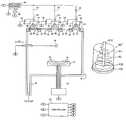
- an embodiment of the system of the invention 10includes a vacuum chamber 14 having a vacuum port 18 connected to a vacuum pump (not shown).
- the system 10includes a series of dielectric windows 26 vacuum sealed by O-rings 30 and attached by removable clamps 34 to the upper surface 22 of the vacuum chamber 14 .
- Removably attached to some of these dielectric windows 26are rf plasma sources 40 , in one embodiment having a helical or pancake antennae 46 located within an outer shield/ground 44 .
- Other embodiments of the antennae using capacitive or inductive couplingmay be used. Cooling of each antenna is accomplished by passing a cooling fluid through the antenna. Cooling is typically required only at higher power.
- the windows 26 without attached rf plasma sources 40are usable as viewing ports into the chamber 14 .
- the removability of each plasma source 40permits the associated dielectric window 26 to be cleaned or the plasma source 40 replaced without the vacuum within the system 10 being removed.
- glass windowsare used in this embodiment, other dielectric material such as quartz or polyethylene may be used for the window material.
- Each antenna 46is connected to a rf generator 66 through a matching network 50 , through a coupling capacitor 54 .
- Each antenna 46also includes a tuning capacitor 58 connected in parallel with its respective antenna 46 .
- Each of the tuning capacitors 58is controlled by a signal D, D′, D′′ from a controller 62 .
- the output power from each rf antenna 46can be adjusted to maintain the uniformity of the plasma generated.
- Other tuning meanssuch as zero reflective power tuning may be also be used to adjust the power to the antennae.
- the rf generator 66is controlled by a signal E from the controller 62 .
- the controller 62controls the power to the antennae 46 by a signal F to the matching network 50 .
- the controller 62adjusts the tuning capacitors 58 and the rf generator 66 in response to a signal A from a sensor 70 (such as a Real Power Monitor by Comdel, Inc., Beverly, Mass.) monitoring the power delivered to the antennae 46 , a signal B from a fast scanning Langmuir probe 74 directly measuring the plasma density and a signal C from a plurality of Faraday cups 78 attached to a substrate wafer holder 82 .
- the Langmuir probe 74is scanned by moving the probe (double arrow I) into and out of the plasma. With these sensors, the settings for the rf generator 66 and the tuning capacitors 58 may be determined by the controller prior to the actual use of the system 10 to plasma treat a substrate.
- the probesare removed and the wafer to be treated is introduced.
- the probesare left in place during processing to permit real time control of the system.
- caremust be taken to not contaminate the plasma with particles evaporating from the probe and to not shadow the substrate being processed.
- the characteristics of the systemare determined at manufacture and the system does not include plasma probes.
- the configuration of plasma sources 40may be such that a plurality of physically smaller plasma sources 40 produce a uniform plasma over an area greater than that of sum of the areas of the individual sources.
- four four-inch diameter plasma sources 40 spaced at the corners of a square at six inch centersproduce a plasma substantially equivalent to that generated by a single twelve inch diameter source. Therefore, by providing a vacuum chamber 14 with a plurality of windows 26 , the various configurations of plasma sources 40 may be formed to produce a uniform plasma of the shape and uniformity desired. Antennae such as those depicted do not result in rf interference between sources when properly shielded as shown.
- Multiple rf plasma sourcescan excite electron cyclotron resonance in the presence of a multi-dipole surface magnetic field.
- a surface magnetic fieldwould, for example, be approximately 1 KG at the pole face and would drop to a few Gauss at about 10 cm. from the pole face.
- the fundamental electron cyclotron resonance frequencyis 13.56 MHz (that is, the frequency supplied by the rf generator) the magnetic field required (as applied by the magnets) is 4.8 G, for resonance coupling to take place.
- the faraday cups 78 used to measure the uniformity of the field and the plasma doseare positioned near one edge in the surface of the wafer holder 82 (FIG. 3 ).
- the flat edge 86 of wafer 90is positioned on the wafer holder 82 such that faraday cups 78 of the wafer holder 82 are exposed to the plasma. In this way the plasma dose experienced by the wafer 90 can be directly measured.
- a special wafer 90 ′is fabricated with a plurality of faraday cups 78 embedded in the wafer 90 ′. This special wafer 90 ′ is used to set the rf generator 66 and the tuning capacitors 58 to achieve the desired plasma density and uniformity. Once the operating parameters have been determined, the special wafer 90 ′ is removed and the wafers 90 to be processed placed on the wafer holder 82 .
- the system 10has been described in terms of a planar array of plasma sources 40 located on the upper surface of the vacuum chamber 14 , the plasma sources 40 may be distributed over other surfaces of the vacuum chamber 14 ′ to generate a uniform volume of plasma. Such a system is particularly effective in batch processing.
- a quartz window 100is not attached to the vacuum chamber 14 , but instead encloses one end of the shield 44 of the plasma source 40 ′.
- a tube 104 attached to an opening 108 in the quartz window 100provides a gas feed to form a plasma of a specific gas.
- the plasma source 40 ′is not attached to a window 26 in the wall of the vacuum chamber 14 , but is instead attached to the vacuum chamber 14 itself.
- Such plasma sources 40 ′can produce plasmas from specific gasses as are required by many processes. Several such plasma sources 40 ′ can be aligned to sequentially treat a wafer 90 with different plasmas as in the embodiment of the inline system shown in FIG. 6 .
- wafers 90are moved by a conveyor 112 through sequential zones, in this embodiment zones I and II, of a continuous processing line 114 . Each zone is separated from the adjacent zones by a baffle 116 .
- the gas in zone Iis SiH 4 used in Si-CVD processing, while the gas in zone II is PH 3 used in doping.
- a cluster tool having load-locks to isolate each processing chamber from the other chambers, and equipped with a robotincludes the rf plasma sources 40 of the invention for plasma CVD and plasma etching.
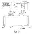
- FIG. 7depicts an embodiment of the system of the invention using two plasma sources.
- each sourceis an inductive pancake antenna 3-4 inches in diameter.
- Each antenna 46is constructed of a 1 ⁇ 4 inch copper tube and contains 5-6 turns.
- Each antenna 46is connected to a matching network 50 through a respective 160 pf capacitor.
- the matching network 50includes a 0.03 ⁇ H inductor 125 and two variable capacitors 130 , 135 .
- One variable capacitor 130is adjustable over the range of 10-250 pf and the second capacitor 135 is adjustable over the range of 5-120 pf.
- the matching network 50is tuned by adjusting the variable capacitor 130 , 135 .
- the matching network 50is in turn connected to an rf source 66 operating at 13.56 mHz.
- a series of magnets 140 , 145are positioned around the circumference of the chamber in alternating polarity every 7 cm to form a magnetic bucket.
- the power to the antenna 46is 25 W per antenna or about 50 W total.
- the power in the chamberreduced to 0.1 m Torr, the power is increased to 200 W per antenna or 400 W total.
- the resulting plasma at 50 W total powerhas a substantially uniform density of 10 11 /cm 3 .
- the uniformity and the densitymay be further improved using four of such sources.
- one embodiment of the arrangement of magnets for ECR generationutilizes a plurality of magnets 150 adjacent the antenna 46 .
- the plurality of the magnets 150is reversed between the antennae.
- FIG. 8 adepicts another embodiment in which each source has its own set of magnets. Other magnet configurations are possible.
- an embodiment of a large area substrateconsists of a high voltage wafer holder 210 on which many wafers 201 can be placed. If the holder 210 is biased at a large negative voltage (DC) and transported along the linear length of the plasma source 220 , a desired ion implantation dose will be reached. This is a simple way to achieve the separation of thin-film silicon layer by ion implantation as used in the Silicon-On-Insulator (SOI) technology. Alternatively, the plasma source 220 could be pulsed and the wafer holder 210 remains stationary to achieve the same effects.
- DCnegative voltage
- SOISilicon-On-Insulator
- the multiple antennae plasma source 200is especially useful for processing of silicon wafers 201 when large ion implantation dosages are desired.
- the throughput of such a systemis extremely large in comparison with any other system including conventional high current beam-line implantation.
- the dosage requiredis 10 16 to 10 17 ions-cm 2 .
- Another techniqueis the Separation by Ion IMplantation of Oxygen (SIMOX) having oxygen implantation dosage of 10 18 ions-cm ⁇ 2 .
- SIMOXSeparation by Ion IMplantation of Oxygen
- Being the best conventional high current ion implantation available in the marketwill require long implantation time, up to several hours.
- Using the large area plasma source 220 and the described process and apparatusallows the implantation time to approach seconds for batch processing of a large number of wafers 201 .
- the first methodincludes pulsing the large area plasma source 220 with a negative high voltage dc bias from the HVDC supply 230 , which is connected to the wafers 201 .
- a negative high voltage dc biasfrom the HVDC supply 230 , which is connected to the wafers 201 .
- all of the ionsare accelerated to the wafer by the electric field at the wafer surface.
- all of the accelerated ionshave the same energy because of the large dc electric field at the wafer surface in comparison to either the plasma potential or the kinetic energy of the ions as the plasma expands.
- the implant dosewill be controlled by the exposure time of the wafer to the plasma, the plasma is turned off when the desired dosage is reached.
- the large plasma sourceallows essentially infinite number of wafer exposure (implantation) at a short time, limited by the available high voltage power rating of the wafer bias. The throughput of such a system is potentially 100 to 1,000 times that of conventional technology.
- FIG. 10shows the dosage relation to the exposure time.
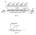
- the second method and apparatusis known as In-line processing, shown in FIG. 11 .
- FIG. 12shows the ion dose relation with the distance or time relationship for this embodiment. Again, the uniformity can be adjusted by controlling the tuning and power level of each rf coil. The throughput of such a system is also extremely high.
- FIG. 14depicts the ion dose and temperature profile of an individual wafer.
- the large area plasma sourceallows a simple connection procedure of the negative high-voltage bias to the wafer and the wafer transport robot system as shown in FIGS. 15 and 16.
- the robot transport system with high voltage connection 270will connect to the wafer holder 275 moving through the plasma for the desired exposure as shown in FIG. 13 and repeat the procedure and send the wafer back for a second batch of exposure.
- Multiple antennae rf sourcesare used to provide a uniform plasma during the pulsing phase and the steady state as to give uniform ion implantation dose to a large area substrate which is biased at a negative voltage.
- other types of excitationdepend on the particular ionization mechanism (i.e. in the case of electron cyclotron resonant ECR source, a resonance ionization process), the location of plasma initiation is often localized. As such, the uniformity of such sources during the turn-on phase is poor. It also takes a long time for such plasma sources to reach steady-state with the desired uniformity (preferably less than 5%) for normal plasma processes.
- the multiple antennae sourcehas multiple ionization locations and are individually tuned by the electronic and tuning circuits.
Landscapes
- Chemical & Material Sciences (AREA)
- Analytical Chemistry (AREA)
- Physics & Mathematics (AREA)
- Engineering & Computer Science (AREA)
- Plasma & Fusion (AREA)
- Plasma Technology (AREA)
- Drying Of Semiconductors (AREA)
- Chemical Vapour Deposition (AREA)
- Crystals, And After-Treatments Of Crystals (AREA)
Abstract
Description
This application is a continuation-in-part application of U.S. Application Ser. No. 08/503,973, filed Jul. 19, 1995, now U.S. Pat. No. 5,653,811.
Not Applicable
Plasma treatment of large area substrates such as glass or semiconductor substrates used in the fabrication of flat panel displays or 300 mm silicon wafers respectively pose a series of problems that do not occur in the processing of small area substrates. One problem is simply the generation of plasmas of sufficient area to treat the large area substrate. A second problem is the maintenance of the uniformity of the plasma density and chemistry over such a large area.
The use of inductively or transformer coupled plasma sources (ICP and TCP, respectively) are affected both by the difficulty of maintaining plasma uniformity using inductive coil antenna designs and the cost of fabricating and maintaining such systems which require large and thick quartz windows for coupling the antenna radiation into the processing chamber. The use of such thick quartz windows results in an increase in rf power (and reduction in efficiency) due to heat dissipation within the window.
The use of Electron Cyclotron Resonance (ECR) and Helicon type sources are limited by the difficulty in scaling the resonant magnetic field to large areas when a single antenna or waveguide is used. Furthermore, most ECR sources utilize microwave power which is more expensive and difficult to tune electrically. The use of hot cathode plasma sources results in the contamination of the plasma environment due to the evaporation of cathode material, while cold cathode sources result in contamination due to exposure of the cold cathode to the plasma generated.
The present invention avoids these problems encountered by previous large area plasma processing systems.
The present invention relates to an easily scalable and maintainable system for producing a uniform plasma of any size. In one embodiment a plurality of rf plasma sources are removably attached to the dielectric windows such as glass or quartz of a vacuum processing chamber, while in another embodiment each of the plurality of sources includes its own window and is attached to the chamber. Plasma measuring probes within the chamber provide information on the plasma uniformity and this information is used to control the rf energy applied to each of the rf plasma sources so as to maintain the desired uniformity. In one embodiment, the plasma measuring probes are Langmuir probes. In another embodiment, the probes are Faraday cups. In yet another embodiment, the probes are optical probes.
In another embodiment, a plasma source includes a quartz window with an integral tube for gas introduction. Several of such plasma sources using different gases may be combined in a linear array for the sequential treatment of substrates in an inline processing system.
In a further embodiment multiple antennae rf sources are used to provide a uniform plasma during the pulsing phase and steady state in order to provide a uniform ion implantation dose to a large area substrate. The plasma source is stationary and the wafers are transported through the plasma or the wafers are stationary and the plasma is transported past the wafers.
This invention is pointed out with particularity in the appended claims. The above and further advantages of this invention may be better understood by referring to the following description taken in conjunction with the accompanying drawing, in which:
FIG. 1 is a block diagram of an embodiment of the plasma treating system of the invention;
FIG. 2 is a top view of a configuration of sources to provide a large area plasma coverage using small area plasma sources;
FIG. 3 is a plan view of an embodiment of a wafer holder with built-in faraday cups;
FIG. 3ais a plan view of an embodiment of a Si test wafer with imbedded faraday cups;
FIG. 4 is a perspective view of an embodiment of the invention configured as a volume source;
FIG. 5 is a perspective view of an embodiment of plasma source of the invention with integral gas feed;
FIG. 6 is a cross-sectional view of an embodiment of a continuous plasma treatment device using a plurality of plasma sources shown in FIG. 5;
FIG. 7 is a schematic diagram of a system utilizing two plasma sources;
FIG. 8 depicts an embodiment of an arrangement of surface magnets for ECR plasma generation in a two source system;
FIG. 8adepicts another embodiment of an arrangement of surface magnets for ECR plasma generation;
FIG. 9 is a diagram of a Separation by Plasma Ion Implantation Technology (SPIT) treatment device;
FIG. 10 is a graph of the ion current (implantation dose) provided by the device of FIG. 9;
FIG. 11 is a diagram of an In-line a plasma processing system;
FIG. 12 is a graph of the ion current (implantation dose) provided by the system of FIG. 11;
FIG. 13 is a diagram of another embodiment of a plasma treatment device;
FIG. 14 is a graph of the ion current (implantation dose) provided by the device of FIG. 13;
FIG. 15 is a diagram of the high voltage connections to the wafer and robot arm of the device of FIG. 11; and
FIG. 16 is a diagram of the high voltage connections to the wafer and robot arm of the device of FIG.13.
In brief overview and referring to FIG. 1, an embodiment of the system of theinvention 10 includes avacuum chamber 14 having avacuum port 18 connected to a vacuum pump (not shown). In the embodiment shown, thesystem 10 includes a series ofdielectric windows 26 vacuum sealed by O-rings 30 and attached byremovable clamps 34 to theupper surface 22 of thevacuum chamber 14. Removably attached to some of thesedielectric windows 26 arerf plasma sources 40, in one embodiment having a helical orpancake antennae 46 located within an outer shield/ground 44. Other embodiments of the antennae using capacitive or inductive coupling may be used. Cooling of each antenna is accomplished by passing a cooling fluid through the antenna. Cooling is typically required only at higher power. Thewindows 26 without attachedrf plasma sources 40 are usable as viewing ports into thechamber 14. The removability of eachplasma source 40 permits the associateddielectric window 26 to be cleaned or theplasma source 40 replaced without the vacuum within thesystem 10 being removed. Although glass windows are used in this embodiment, other dielectric material such as quartz or polyethylene may be used for the window material.
Eachantenna 46 is connected to arf generator 66 through amatching network 50, through acoupling capacitor 54. Eachantenna 46 also includes atuning capacitor 58 connected in parallel with itsrespective antenna 46. Each of thetuning capacitors 58 is controlled by a signal D, D′, D″ from acontroller 62. By individually adjusting thetuning capacitors 58 the output power from eachrf antenna 46 can be adjusted to maintain the uniformity of the plasma generated. Other tuning means such as zero reflective power tuning may be also be used to adjust the power to the antennae. In one embodiment, therf generator 66 is controlled by a signal E from thecontroller 62. In one embodiment, thecontroller 62 controls the power to theantennae 46 by a signal F to thematching network 50.
Thecontroller 62 adjusts thetuning capacitors 58 and therf generator 66 in response to a signal A from a sensor70 (such as a Real Power Monitor by Comdel, Inc., Beverly, Mass.) monitoring the power delivered to theantennae 46, a signal B from a fastscanning Langmuir probe 74 directly measuring the plasma density and a signal C from a plurality of Faraday cups78 attached to asubstrate wafer holder 82. TheLangmuir probe 74 is scanned by moving the probe (double arrow I) into and out of the plasma. With these sensors, the settings for therf generator 66 and thetuning capacitors 58 may be determined by the controller prior to the actual use of thesystem 10 to plasma treat a substrate. Once the settings are determined, the probes are removed and the wafer to be treated is introduced. In another embodiment of the system, the probes are left in place during processing to permit real time control of the system. In such an embodiment using a Langmuir probe, care must be taken to not contaminate the plasma with particles evaporating from the probe and to not shadow the substrate being processed. In yet another embodiment of the system, the characteristics of the system are determined at manufacture and the system does not include plasma probes.
Referring to FIG. 2, the configuration ofplasma sources 40 may be such that a plurality of physicallysmaller plasma sources 40 produce a uniform plasma over an area greater than that of sum of the areas of the individual sources. In the embodiment of the configuration shown, four four-inchdiameter plasma sources 40 spaced at the corners of a square at six inch centers produce a plasma substantially equivalent to that generated by a single twelve inch diameter source. Therefore, by providing avacuum chamber 14 with a plurality ofwindows 26, the various configurations ofplasma sources 40 may be formed to produce a uniform plasma of the shape and uniformity desired. Antennae such as those depicted do not result in rf interference between sources when properly shielded as shown.
Multiple rf plasma sources can excite electron cyclotron resonance in the presence of a multi-dipole surface magnetic field. Such a surface magnetic field would, for example, be approximately 1 KG at the pole face and would drop to a few Gauss at about 10 cm. from the pole face. In such a system, electron cyclotron resonance may be established, with the electron cyclotron resonance frequency (in Hz) being given by the expression ν=2.8×10⁶(B) where B is the magnetic field strength in Gauss. Thus, if the fundamental electron cyclotron resonance frequency is 13.56 MHz (that is, the frequency supplied by the rf generator) the magnetic field required (as applied by the magnets) is 4.8 G, for resonance coupling to take place. Higher harmonics of the fundamental resonance frequency may be achieved by increasing the magnetic field proportionately. Thus for a second harmonic to be coupled, the magnetic field would have to be increased to 9.6 G. Such ECR coupling is most effective at lower pressures (P<1 mTorr). The use of the small rf plasma sources permit such magnets to be positioned so as to make electron cyclotron resonance possible.
The faraday cups78 used to measure the uniformity of the field and the plasma dose, in one embodiment, are positioned near one edge in the surface of the wafer holder82 (FIG.3). Theflat edge 86 ofwafer 90 is positioned on thewafer holder 82 such that faraday cups78 of thewafer holder 82 are exposed to the plasma. In this way the plasma dose experienced by thewafer 90 can be directly measured. Alternatively, aspecial wafer 90′, as shown in FIG. 3a, is fabricated with a plurality of faraday cups78 embedded in thewafer 90′. Thisspecial wafer 90′ is used to set therf generator 66 and thetuning capacitors 58 to achieve the desired plasma density and uniformity. Once the operating parameters have been determined, thespecial wafer 90′ is removed and thewafers 90 to be processed placed on thewafer holder 82.
Referring to FIG. 4, although thesystem 10 has been described in terms of a planar array ofplasma sources 40 located on the upper surface of thevacuum chamber 14, theplasma sources 40 may be distributed over other surfaces of thevacuum chamber 14′ to generate a uniform volume of plasma. Such a system is particularly effective in batch processing.
Referring to FIG. 5, in another embodiment, aquartz window 100 is not attached to thevacuum chamber 14, but instead encloses one end of theshield 44 of theplasma source 40′. In this embodiment, atube 104 attached to anopening 108 in thequartz window 100 provides a gas feed to form a plasma of a specific gas. In this case, theplasma source 40′ is not attached to awindow 26 in the wall of thevacuum chamber 14, but is instead attached to thevacuum chamber 14 itself.Such plasma sources 40′ can produce plasmas from specific gasses as are required by many processes. Severalsuch plasma sources 40′ can be aligned to sequentially treat awafer 90 with different plasmas as in the embodiment of the inline system shown in FIG.6. In this embodiment,wafers 90 are moved by aconveyor 112 through sequential zones, in this embodiment zones I and II, of acontinuous processing line 114. Each zone is separated from the adjacent zones by abaffle 116. In one embodiment, the gas in zone I is SiH4used in Si-CVD processing, while the gas in zone II is PH3used in doping. In another embodiment, a cluster tool having load-locks to isolate each processing chamber from the other chambers, and equipped with a robot includes therf plasma sources 40 of the invention for plasma CVD and plasma etching.
FIG. 7 depicts an embodiment of the system of the invention using two plasma sources. In this embodiment each source is an inductive pancake antenna 3-4 inches in diameter. Eachantenna 46 is constructed of a ¼ inch copper tube and contains 5-6 turns. Eachantenna 46 is connected to amatching network 50 through a respective 160 pf capacitor. Thematching network 50 includes a 0.03μH inductor 125 and two variable capacitors130,135. One variable capacitor130 is adjustable over the range of 10-250 pf and the second capacitor135 is adjustable over the range of 5-120 pf. Thematching network 50 is tuned by adjusting the variable capacitor130,135. Thematching network 50 is in turn connected to anrf source 66 operating at 13.56 mHz. A series ofmagnets
With the chamber operating at 1 m Torr pressure, the power to theantenna 46 is 25 W per antenna or about 50 W total. With the pressure in the chamber reduced to 0.1 m Torr, the power is increased to 200 W per antenna or 400 W total. The resulting plasma at 50 W total power has a substantially uniform density of 1011/cm3. The uniformity and the density may be further improved using four of such sources.
Referring to FIG. 8, one embodiment of the arrangement of magnets for ECR generation utilizes a plurality ofmagnets 150 adjacent theantenna 46. In this embodiment, the plurality of themagnets 150 is reversed between the antennae. FIG. 8adepicts another embodiment in which each source has its own set of magnets. Other magnet configurations are possible.
Referring to FIG. 9, an embodiment of a large area substrate consists of a highvoltage wafer holder 210 on whichmany wafers 201 can be placed. If theholder 210 is biased at a large negative voltage (DC) and transported along the linear length of theplasma source 220, a desired ion implantation dose will be reached. This is a simple way to achieve the separation of thin-film silicon layer by ion implantation as used in the Silicon-On-Insulator (SOI) technology. Alternatively, theplasma source 220 could be pulsed and thewafer holder 210 remains stationary to achieve the same effects.
The multipleantennae plasma source 200 is especially useful for processing ofsilicon wafers 201 when large ion implantation dosages are desired. The throughput of such a system is extremely large in comparison with any other system including conventional high current beam-line implantation. For example, a particular thin-film transfer technique using hydrogen ion implantation into Si-wafer to separate the top silicon layer with the bulk wafer via hydrogen ion embitterment. The dosage required is 1016to 1017ions-cm2. Another technique is the Separation by Ion IMplantation of Oxygen (SIMOX) having oxygen implantation dosage of 1018ions-cm−2. Being the best conventional high current ion implantation available in the market will require long implantation time, up to several hours. Using the largearea plasma source 220 and the described process and apparatus allows the implantation time to approach seconds for batch processing of a large number ofwafers 201.
Two methods can be used for the batch processing of wafers. The first method includes pulsing the largearea plasma source 220 with a negative high voltage dc bias from theHVDC supply 230, which is connected to thewafers 201. When the plasma forms and expands to the wafers, all of the ions are accelerated to the wafer by the electric field at the wafer surface. As a result, all of the accelerated ions have the same energy because of the large dc electric field at the wafer surface in comparison to either the plasma potential or the kinetic energy of the ions as the plasma expands. As the implant dose will be controlled by the exposure time of the wafer to the plasma, the plasma is turned off when the desired dosage is reached. The large plasma source allows essentially infinite number of wafer exposure (implantation) at a short time, limited by the available high voltage power rating of the wafer bias. The throughput of such a system is potentially 100 to 1,000 times that of conventional technology.
The uniformity of the implant can be controlled precisely as the individual rf coils can be tuned separately for the optimum plasma uniformity. FIG. 10 shows the dosage relation to the exposure time.
The second method and apparatus is known as In-line processing, shown in FIG.11. The largearea plasma source 260 is operated steady-state and thewafers 201 are moving from one end to the other end as the exposure time t=S/V where S is the length of the plasma (linear length of the plasma source) and V is the speed of the wafer transport. FIG. 12 shows the ion dose relation with the distance or time relationship for this embodiment. Again, the uniformity can be adjusted by controlling the tuning and power level of each rf coil. The throughput of such a system is also extremely high.
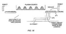
In such a system, with the adjusting of the plasma density and the ion dosage per sec (dose rate), it's possible to control the wafer temperature precisely (with and without external wafer cooling means). A simplified version of the in-line system, shown in FIG. 13, can also be used which results in simple equipment design and which will not need wafer cooling for most SPIT applications. FIG. 14 depicts the ion dose and temperature profile of an individual wafer. In such a system, the large area plasma source allows a simple connection procedure of the negative high-voltage bias to the wafer and the wafer transport robot system as shown in FIGS. 15 and 16.
After the wafers are loaded in the loading port (FIG.13), the robot transport system withhigh voltage connection 270 will connect to thewafer holder 275 moving through the plasma for the desired exposure as shown in FIG.13 and repeat the procedure and send the wafer back for a second batch of exposure.
Multiple antennae rf sources are used to provide a uniform plasma during the pulsing phase and the steady state as to give uniform ion implantation dose to a large area substrate which is biased at a negative voltage. When the plasma is pulsed on, other types of excitation depend on the particular ionization mechanism (i.e. in the case of electron cyclotron resonant ECR source, a resonance ionization process), the location of plasma initiation is often localized. As such, the uniformity of such sources during the turn-on phase is poor. It also takes a long time for such plasma sources to reach steady-state with the desired uniformity (preferably less than 5%) for normal plasma processes. The multiple antennae source has multiple ionization locations and are individually tuned by the electronic and tuning circuits. As such, a uniform plasma is provided from the pulsing phase all the way to steady state by control of the individual antenna. This is done precisely with the feedback scheme disclosed in co-pending U.S. patent application Ser. No. 08/503,973, the disclosure of which is incorporated herein by reference.
Having shown the preferred embodiment, those skilled in the art will realize many variations are possible which will still be within the scope and spirit of the claimed invention. Therefore, it is the intention to limit the invention only as indicated by the scope of the claims.
Claims (28)
1. A system for processing a substrate, said system comprising:
a vacuum chamber in which a plasma is generated;
a first dielectric window on a surface of said chamber, said dielectric window having a first side and a second side facing outside and inside of said chamber, respectively;
an rf generator;
a sensor to monitor a process condition as said substrate is being processed in said chamber and transmit a signal in response to said monitored process condition;
a controller to receive said signal from said sensor and adjust at least one process parameter; and
a removable plasma source located external to said vacuum chamber, said plasma source electrically coupled to said rf generator and operative to generate a plasma, said plasma source including an antenna provided over said first side of said first dielectric window, said antenna having a plurality of spiral portions extending in a substantially orthogonal direction from said dielectric window.
2. The system ofclaim 1 wherein said plasma source is a pulsed plasma source.
3. The system ofclaim 1 wherein said plasma source is a steady-state plasma source.
4. The system ofclaim 1 wherein said system has a plurality of dielectric windows and a plurality of plasma sources.
5. The system ofclaim 4 , wherein each of said plurality of plasma sources is configured to be tuned, so that each plasma source may be tuned in order to provide a plasma of the shape and uniformity desired for a particular process.
6. The system ofclaim 1 wherein said plasma source comprises a shield having an opening that faces said first side of said dielectric window, said shield cooperating with said first side of said dielectric window to enclose said antenna.
7. The system ofclaim 1 , wherein said first dielectric window is constructed of quartz.
8. The system ofclaim 1 , wherein said first dielectric window is constructed of glass.
9. The system ofclaim 1 , further comprising:
a voltage substrate holder configured to receive a plurality of substrates and provide bias to said plurality of substrates to facilitate implantation of ions into said plurality of substrates.
10. The system ofclaim 9 , further comprising:
a conveyor to transport said plurality of substrates from a first point to a second point within said chamber;
a loading dock to receive said plurality of substrates and transport said plurality of substrates into said chamber; and
an unload dock to receive said plurality of substrates from said chamber after said plurality of substrates has been processed in said chamber,
wherein said chamber includes a plurality of process zones.
11. The system ofclaim 1 , further comprising:
conveyor to transport said substrate from a first point to a second point within said chamber;
a loading dock to receive said substrate and transport said substrate into said chamber; and
an unload dock to receive said substrate from said chamber after said substrate has been processed in said chamber,
wherein said chamber includes a plurality of process zones and
each of said process zone performs a different process on said substrate.
12. The system ofclaim 11 , wherein a first zone of said plurality of zones performs a chemical vapor deposition said substrate.
13. The system ofclaim 12 wherein a second zone of said plurality of zones an ion implantation on said substrate.
14. The system ofclaim 11 , further comprising a baffle to separate said ones.
15. The system ofclaim 1 , further comprising a bias power supply operative to bias said substrate.
16. The system ofclaim 1 , further comprising:
a second dielectric window provided over a substrate receiver configured to receive a substrate, said second dielectric window being configured to be a viewing port to view said substrate provided within said chamber on said substrate receiver, said second dielectric window being free of a plasma source.
17. The system ofclaim 1 , wherein said plasma source located external to said chamber is configured to be replaced without disturbing the vacuum within said chamber.
18. The system ofclaim 1 , wherein said plurality of spiral portions of said antenna includes a first spiral portion that is proximate to said first dielectric window and a second spiral portion that is remote from said first dielectric window, said first spiral portion having a greater diameter than said second spiral portion.
19. The system ofclaim 18 , further comprising: a gas feed tube extending through said antenna in said substantially orthogonal direction from said first dielectric window, so that said first spiral portion wraps around a first extending portion of said feed tube and said second spiral portion wraps around a second extending portion of said feed tube that is different from said first extending portion.
20. The system ofclaim 19 , wherein said antenna has 5 or 6 turns to define 5 or 6 portions.
21. The system ofclaim 1 , wherein said antenna is a copper tube having diameter of ¼ inch.
22. The system ofclaim 1 , further comprising:
a plurality of plasma sources provided on a side wall of said chamber; and
a plurality of plasma sources provided on an upper surface of said chamber.
23. The system ofclaim 1 , further comprising:
a plurality of plasma sources provided on an upper surface of said chamber;
a high voltage substrate receiver configured to receive a plurality of substrates and provide bias to said plurality of substrates to facilitate implantation of ions into said plurality of substrates.
24. The system ofclaim 23 , wherein each of said plurality of plasma sources are configured to be tuned in cooperation with each other to provide a plasma having a uniform shape within said chamber to process said plurality of substrate.
25. The system ofclaim 1 , wherein said first dielectric window is configured to be viewing port into said chamber if said plasma source is removed from said first window.
26. A system for processing a substrate, comprising:
a vacuum chamber in which a plasma is generated;
a first dielectric window on a surface of said chamber, said first dielectric window having a first side and a second side facing outside and inside of said chamber, respectively;
a second dielectric window configured as a viewing port;
an rf generator;
a control system to monitor and adjust a process condition within said chamber; and
a plasma source located external to said vacuum chamber, said plasma source electrically coupled to said rf generator and operative to generate a plasma, said plasma source including a vertically-extending, removable antenna provided over said first side of said first dielectric window and a shield having an opening that faces said first side of said first dielectric window, said shield cooperating with said first side of said first dielectric window to enclose said antenna, said vertically extending antenna having first, second, and third spiral portions; and
a gas feed tube extending through said antenna and having a first extending portion proximate to said first dielectric window and a second extending portion remote from said first dielectric window,
wherein said first spiral portion wraps around said first extending portion of said feed tube and said second spiral portion wraps around said second extending portion, and
wherein said antenna and shield are removably attached to said dielectric window.
27. The system ofclaim 26 , wherein said antenna and shield configured to be removed to clean the dielectric window without disturbing a vacuum environment of the chamber.
28. The system ofclaim 26 , wherein said antenna is configured to be replaced with another antenna without disturbing a vacuum environment of the chamber.
Priority Applications (2)
| Application Number | Priority Date | Filing Date | Title |
|---|---|---|---|
| US08/878,005US6632324B2 (en) | 1995-07-19 | 1997-06-18 | System for the plasma treatment of large area substrates |
| US09/065,953US6338313B1 (en) | 1995-07-19 | 1998-04-24 | System for the plasma treatment of large area substrates |
Applications Claiming Priority (2)
| Application Number | Priority Date | Filing Date | Title |
|---|---|---|---|
| US08/503,973US5653811A (en) | 1995-07-19 | 1995-07-19 | System for the plasma treatment of large area substrates |
| US08/878,005US6632324B2 (en) | 1995-07-19 | 1997-06-18 | System for the plasma treatment of large area substrates |
Related Parent Applications (1)
| Application Number | Title | Priority Date | Filing Date |
|---|---|---|---|
| US08/503,973Continuation-In-PartUS5653811A (en) | 1995-07-19 | 1995-07-19 | System for the plasma treatment of large area substrates |
Related Child Applications (1)
| Application Number | Title | Priority Date | Filing Date |
|---|---|---|---|
| US09/065,953ContinuationUS6338313B1 (en) | 1995-07-19 | 1998-04-24 | System for the plasma treatment of large area substrates |
Publications (2)
| Publication Number | Publication Date |
|---|---|
| US20020029850A1 US20020029850A1 (en) | 2002-03-14 |
| US6632324B2true US6632324B2 (en) | 2003-10-14 |
Family
ID=24004315
Family Applications (3)
| Application Number | Title | Priority Date | Filing Date |
|---|---|---|---|
| US08/503,973Expired - LifetimeUS5653811A (en) | 1995-07-19 | 1995-07-19 | System for the plasma treatment of large area substrates |
| US08/878,005Expired - Fee RelatedUS6632324B2 (en) | 1995-07-19 | 1997-06-18 | System for the plasma treatment of large area substrates |
| US09/065,953Expired - LifetimeUS6338313B1 (en) | 1995-07-19 | 1998-04-24 | System for the plasma treatment of large area substrates |
Family Applications Before (1)
| Application Number | Title | Priority Date | Filing Date |
|---|---|---|---|
| US08/503,973Expired - LifetimeUS5653811A (en) | 1995-07-19 | 1995-07-19 | System for the plasma treatment of large area substrates |
Family Applications After (1)
| Application Number | Title | Priority Date | Filing Date |
|---|---|---|---|
| US09/065,953Expired - LifetimeUS6338313B1 (en) | 1995-07-19 | 1998-04-24 | System for the plasma treatment of large area substrates |
Country Status (9)
| Country | Link |
|---|---|
| US (3) | US5653811A (en) |
| EP (1) | EP0842307B1 (en) |
| JP (1) | JP4128217B2 (en) |
| KR (1) | KR19990029069A (en) |
| CN (1) | CN1192788A (en) |
| AU (1) | AU718941B2 (en) |
| CA (1) | CA2227233C (en) |
| DE (1) | DE69625068D1 (en) |
| WO (1) | WO1997004478A2 (en) |
Cited By (53)
| Publication number | Priority date | Publication date | Assignee | Title |
|---|---|---|---|---|
| US20040166612A1 (en)* | 2002-06-05 | 2004-08-26 | Applied Materials, Inc. | Fabrication of silicon-on-insulator structure using plasma immersion ion implantation |
| US20050208316A1 (en)* | 2004-03-19 | 2005-09-22 | Younger Mfg. Co. Dba Younger Optics | Polyvinyl alcohol-based film exhibiting improved adhesion and method for making it |
| US20050220245A1 (en)* | 2001-02-01 | 2005-10-06 | The Regents Of The University Of California | Formation of a field reversed configuration for magnetic and electrostatic confinement of plasma |
| US20050258767A1 (en)* | 2001-03-19 | 2005-11-24 | The Regents Of The University Of California | Controlled fusion in a field reversed configuration and direct energy conversion |
| US20060144520A1 (en)* | 2002-09-19 | 2006-07-06 | Tokyo Electron Limited | Viewing window cleaning apparatus |
| US20060198485A1 (en)* | 2005-03-07 | 2006-09-07 | Michl Binderbauer | Plasma electric generation and propulsion system |
| US20060264004A1 (en)* | 2005-05-23 | 2006-11-23 | Ziptronix, Inc. | Method of detachable direct bonding at low temperatures |
| US20060267503A1 (en)* | 2005-03-07 | 2006-11-30 | Vitaly Bystriskii | Inductive plasma source for plasma electric generation system |
| US20060267504A1 (en)* | 2005-03-07 | 2006-11-30 | Vandrie Alan | Vacuum chamber for plasma electric generation system |
| US7183177B2 (en) | 2000-08-11 | 2007-02-27 | Applied Materials, Inc. | Silicon-on-insulator wafer transfer method using surface activation plasma immersion ion implantation for wafer-to-wafer adhesion enhancement |
| US20070127542A1 (en)* | 2005-12-07 | 2007-06-07 | Ajax Tocco Magnethermic Corporation | Induction coil having internal and external faradic rings |
| US7294563B2 (en) | 2000-08-10 | 2007-11-13 | Applied Materials, Inc. | Semiconductor on insulator vertical transistor fabrication and doping process |
| US7305935B1 (en) | 2004-08-25 | 2007-12-11 | The United States Of America As Represented By The Administration Of Nasa | Slotted antenna waveguide plasma source |
| US20080044257A1 (en)* | 2006-08-15 | 2008-02-21 | Varian Semiconductor Equipment Associates, Inc. | Techniques for temperature-controlled ion implantation |
| US20080050292A1 (en)* | 2006-08-28 | 2008-02-28 | Valery Godyak | Plasma reactor with inductie excitation of plasma and efficient removal of heat from the excitation coil |
| US20080050537A1 (en)* | 2006-08-22 | 2008-02-28 | Valery Godyak | Inductive plasma source with high coupling efficiency |
| US7400096B1 (en) | 2004-07-19 | 2008-07-15 | The United States Of America As Represented By The Administrator Of The National Aeronautics And Space Administration | Large area plasma source |
| US20090081811A1 (en)* | 2007-06-29 | 2009-03-26 | Neil Benjamin | Distributed power arrangements for localizing power delivery |
| US20090078677A1 (en)* | 2007-06-29 | 2009-03-26 | Neil Benjamin | Integrated steerability array arrangement for minimizing non-uniformity |
| US7927975B2 (en) | 2009-02-04 | 2011-04-19 | Micron Technology, Inc. | Semiconductor material manufacture |
| WO2011059749A3 (en)* | 2009-10-28 | 2011-09-09 | Applied Materials, Inc. | Vertically integrated processing chamber |
| US20110241547A1 (en)* | 2008-12-09 | 2011-10-06 | Gang Wei | Plasma processing apparatus |
| US20110259523A1 (en)* | 2008-12-09 | 2011-10-27 | Tokyo Electron Limited | Plasma processing apparatus |
| US20130093321A1 (en)* | 2010-03-31 | 2013-04-18 | Tokyo Electron Limited | Dielectric window for plasma processing apparatus, plasma processing apparatus and method for mounting dielectric window for plasma processing apparatus |
| US20130108491A1 (en)* | 2009-06-25 | 2013-05-02 | Omax Corporation | Reciprocating pump and method for making a system with enhanced dynamic seal reliability |
| WO2014028290A1 (en)* | 2012-08-13 | 2014-02-20 | Varian Semiconductor Equipment Associates, Inc. | Inductively coupled plasma ion source with multiple antennas for wide ion beam |
| US8697552B2 (en) | 2009-06-23 | 2014-04-15 | Intevac, Inc. | Method for ion implant using grid assembly |
| US8697553B2 (en) | 2008-06-11 | 2014-04-15 | Intevac, Inc | Solar cell fabrication with faceting and ion implantation |
| US20150108894A1 (en)* | 2013-10-17 | 2015-04-23 | Varian Semiconductor Equipment Associates, Inc. | Wide metal-free plasma flood gun |
| US9123512B2 (en) | 2005-03-07 | 2015-09-01 | The Regents Of The Unviersity Of California | RF current drive for plasma electric generation system |
| US9318332B2 (en) | 2012-12-19 | 2016-04-19 | Intevac, Inc. | Grid for plasma ion implant |
| US9324598B2 (en) | 2011-11-08 | 2016-04-26 | Intevac, Inc. | Substrate processing system and method |
| US9336997B2 (en) | 2014-03-17 | 2016-05-10 | Applied Materials, Inc. | RF multi-feed structure to improve plasma uniformity |
| US9355819B2 (en) | 2013-08-16 | 2016-05-31 | Applied Materials, Inc. | Elongated capacitively coupled plasma source for high temperature low pressure environments |
| US20160163511A1 (en)* | 2014-12-08 | 2016-06-09 | Applied Materials, Inc. | Tunable magnetic field to improve uniformity |
| US20170323766A1 (en)* | 2016-05-03 | 2017-11-09 | Vni Solution Co., Ltd. | Rf antenna structure for inductively coupled plasma processing apparatus |
| US9997261B2 (en) | 2011-11-14 | 2018-06-12 | The Regents Of The University Of California | Systems and methods for forming and maintaining a high performance FRC |
| US10049774B2 (en) | 2013-09-24 | 2018-08-14 | Tae Technologies, Inc. | Systems and methods for forming and maintaining a high performance FRC |
| US10217532B2 (en) | 2014-10-13 | 2019-02-26 | Tae Technologies, Inc. | Systems and methods for merging and compressing compact tori |
| US10332727B2 (en)* | 2009-12-03 | 2019-06-25 | Lam Research Corporation | Methods for processing substrates using small plasma chambers |
| US10418170B2 (en) | 2015-05-12 | 2019-09-17 | Tae Technologies, Inc. | Systems and methods for reducing undesired eddy currents |
| US10440806B2 (en) | 2014-10-30 | 2019-10-08 | Tae Technologies, Inc. | Systems and methods for forming and maintaining a high performance FRC |
| US10808688B1 (en) | 2017-07-03 | 2020-10-20 | Omax Corporation | High pressure pumps having a check valve keeper and associated systems and methods |
| US20200343087A1 (en)* | 2018-09-28 | 2020-10-29 | Taiwan Semiconductor Manufacturing Co., Ltd. | Pre-Clean for Contacts |
| US11037765B2 (en)* | 2018-07-03 | 2021-06-15 | Tokyo Electron Limited | Resonant structure for electron cyclotron resonant (ECR) plasma ionization |
| US11195627B2 (en) | 2016-10-28 | 2021-12-07 | Tae Technologies, Inc. | Systems and methods for improved sustainment of a high performance FRC plasma at elevated energies utilizing neutral beam injectors with tunable beam energies |
| US11211172B2 (en) | 2016-11-04 | 2021-12-28 | Tae Technologies, Inc. | Systems and methods for improved sustainment of a high performance FRC with multi-scaled capture type vacuum pumping |
| US11217351B2 (en) | 2015-11-13 | 2022-01-04 | Tae Technologies, Inc. | Systems and methods for FRC plasma position stability |
| US11335467B2 (en) | 2016-11-15 | 2022-05-17 | Tae Technologies, Inc. | Systems and methods for improved sustainment of a high performance FRC and high harmonic fast wave electron heating in a high performance FRC |
| US11776793B2 (en) | 2020-11-13 | 2023-10-03 | Applied Materials, Inc. | Plasma source with ceramic electrode plate |
| US11904494B2 (en) | 2020-03-30 | 2024-02-20 | Hypertherm, Inc. | Cylinder for a liquid jet pump with multi-functional interfacing longitudinal ends |
| US12394604B2 (en) | 2020-09-11 | 2025-08-19 | Applied Materials, Inc. | Plasma source with floating electrodes |
| US12432840B2 (en) | 2020-01-13 | 2025-09-30 | Tae Technologies, Inc. | System and methods for forming and maintaining high energy and temperature FRC plasma via spheromak merging and neutral beam injection |
Families Citing this family (152)
| Publication number | Priority date | Publication date | Assignee | Title |
|---|---|---|---|---|
| US6074512A (en)* | 1991-06-27 | 2000-06-13 | Applied Materials, Inc. | Inductively coupled RF plasma reactor having an overhead solenoidal antenna and modular confinement magnet liners |
| US5653811A (en)* | 1995-07-19 | 1997-08-05 | Chan; Chung | System for the plasma treatment of large area substrates |
| US5907221A (en)* | 1995-08-16 | 1999-05-25 | Applied Materials, Inc. | Inductively coupled plasma reactor with an inductive coil antenna having independent loops |
| JP4654176B2 (en)* | 1996-02-22 | 2011-03-16 | 住友精密工業株式会社 | Inductively coupled plasma reactor |
| US6116185A (en)* | 1996-05-01 | 2000-09-12 | Rietzel; James G. | Gas injector for plasma enhanced chemical vapor deposition |
| JP3437376B2 (en)* | 1996-05-21 | 2003-08-18 | キヤノン株式会社 | Plasma processing apparatus and processing method |
| US5846883A (en)* | 1996-07-10 | 1998-12-08 | Cvc, Inc. | Method for multi-zone high-density inductively-coupled plasma generation |
| US6140773A (en)* | 1996-09-10 | 2000-10-31 | The Regents Of The University Of California | Automated control of linear constricted plasma source array |
| KR100505176B1 (en) | 1996-09-27 | 2005-10-10 | 서페이스 테크놀로지 시스템스 피엘씨 | Plasma Processing Equipment |
| GB9620151D0 (en) | 1996-09-27 | 1996-11-13 | Surface Tech Sys Ltd | Plasma processing apparatus |
| US6534922B2 (en) | 1996-09-27 | 2003-03-18 | Surface Technology Systems, Plc | Plasma processing apparatus |
| US6035868A (en)* | 1997-03-31 | 2000-03-14 | Lam Research Corporation | Method and apparatus for control of deposit build-up on an inner surface of a plasma processing chamber |
| US6033974A (en) | 1997-05-12 | 2000-03-07 | Silicon Genesis Corporation | Method for controlled cleaving process |
| US20070122997A1 (en) | 1998-02-19 | 2007-05-31 | Silicon Genesis Corporation | Controlled process and resulting device |
| US6291313B1 (en) | 1997-05-12 | 2001-09-18 | Silicon Genesis Corporation | Method and device for controlled cleaving process |
| US6245161B1 (en)* | 1997-05-12 | 2001-06-12 | Silicon Genesis Corporation | Economical silicon-on-silicon hybrid wafer assembly |
| US6027988A (en)* | 1997-05-28 | 2000-02-22 | The Regents Of The University Of California | Method of separating films from bulk substrates by plasma immersion ion implantation |
| GB9711273D0 (en) | 1997-06-03 | 1997-07-30 | Trikon Equip Ltd | Electrostatic chucks |
| US6158384A (en)* | 1997-06-05 | 2000-12-12 | Applied Materials, Inc. | Plasma reactor with multiple small internal inductive antennas |
| US6178920B1 (en) | 1997-06-05 | 2001-01-30 | Applied Materials, Inc. | Plasma reactor with internal inductive antenna capable of generating helicon wave |
| US5989349A (en)* | 1997-06-24 | 1999-11-23 | Applied Materials, Inc. | Diagnostic pedestal assembly for a semiconductor wafer processing system |
| US6548382B1 (en) | 1997-07-18 | 2003-04-15 | Silicon Genesis Corporation | Gettering technique for wafers made using a controlled cleaving process |
| US6136165A (en)* | 1997-11-26 | 2000-10-24 | Cvc Products, Inc. | Apparatus for inductively-coupled-plasma-enhanced ionized physical-vapor deposition |
| US6217724B1 (en)* | 1998-02-11 | 2001-04-17 | Silicon General Corporation | Coated platen design for plasma immersion ion implantation |
| US6186091B1 (en)* | 1998-02-11 | 2001-02-13 | Silicon Genesis Corporation | Shielded platen design for plasma immersion ion implantation |
| US6269765B1 (en)* | 1998-02-11 | 2001-08-07 | Silicon Genesis Corporation | Collection devices for plasma immersion ion implantation |
| US6120660A (en)* | 1998-02-11 | 2000-09-19 | Silicon Genesis Corporation | Removable liner design for plasma immersion ion implantation |
| US6228176B1 (en)* | 1998-02-11 | 2001-05-08 | Silicon Genesis Corporation | Contoured platen design for plasma immerson ion implantation |
| US6274459B1 (en) | 1998-02-17 | 2001-08-14 | Silicon Genesis Corporation | Method for non mass selected ion implant profile control |
| US6034781A (en)* | 1998-05-26 | 2000-03-07 | Wisconsin Alumni Research Foundation | Electro-optical plasma probe |
| US6291326B1 (en) | 1998-06-23 | 2001-09-18 | Silicon Genesis Corporation | Pre-semiconductor process implant and post-process film separation |
| US6300643B1 (en) | 1998-08-03 | 2001-10-09 | Varian Semiconductor Equipment Associates, Inc. | Dose monitor for plasma doping system |
| US6020592A (en) | 1998-08-03 | 2000-02-01 | Varian Semiconductor Equipment Associates, Inc. | Dose monitor for plasma doping system |
| US6050218A (en)* | 1998-09-28 | 2000-04-18 | Eaton Corporation | Dosimetry cup charge collection in plasma immersion ion implantation |
| JP2002531914A (en)* | 1998-12-01 | 2002-09-24 | シリコン ジェネシス コーポレイション | Enhanced plasma mode, method and system for plasma immersion ion implantation |
| US6300227B1 (en) | 1998-12-01 | 2001-10-09 | Silicon Genesis Corporation | Enhanced plasma mode and system for plasma immersion ion implantation |
| EP1147242A4 (en) | 1998-12-30 | 2007-05-02 | Tokyo Electron Ltd | Large area plasma source |
| KR100745495B1 (en)* | 1999-03-10 | 2007-08-03 | 동경 엘렉트론 주식회사 | Semiconductor manufacturing method and semiconductor manufacturing apparatus |
| US6458723B1 (en) | 1999-06-24 | 2002-10-01 | Silicon Genesis Corporation | High temperature implant apparatus |
| US6199506B1 (en)* | 1999-06-30 | 2001-03-13 | Novellus Systems, Inc. | Radio frequency supply circuit for in situ cleaning of plasma-enhanced chemical vapor deposition chamber using NF3 or NF3/He mixture |
| WO2001011659A1 (en)* | 1999-08-06 | 2001-02-15 | Axcelis Technologies, Inc. | System and method for providing implant dose uniformity across the surface of a substrate |
| US6500732B1 (en) | 1999-08-10 | 2002-12-31 | Silicon Genesis Corporation | Cleaving process to fabricate multilayered substrates using low implantation doses |
| US6221740B1 (en) | 1999-08-10 | 2001-04-24 | Silicon Genesis Corporation | Substrate cleaving tool and method |
| AU6905000A (en) | 1999-08-10 | 2001-03-05 | Silicon Genesis Corporation | A cleaving process to fabricate multilayered substrates using low implantation doses |
| US6263941B1 (en) | 1999-08-10 | 2001-07-24 | Silicon Genesis Corporation | Nozzle for cleaving substrates |
| US6706541B1 (en) | 1999-10-20 | 2004-03-16 | Advanced Micro Devices, Inc. | Method and apparatus for controlling wafer uniformity using spatially resolved sensors |
| JP3645768B2 (en)* | 1999-12-07 | 2005-05-11 | シャープ株式会社 | Plasma process equipment |
| KR100323613B1 (en)* | 2000-03-29 | 2002-02-19 | 박세근 | Apparatus for generating a large area plasma source |
| US6653852B1 (en)* | 2000-03-31 | 2003-11-25 | Lam Research Corporation | Wafer integrated plasma probe assembly array |
| US6685798B1 (en)* | 2000-07-06 | 2004-02-03 | Applied Materials, Inc | Plasma reactor having a symmetrical parallel conductor coil antenna |
| US6578514B2 (en)* | 2000-07-13 | 2003-06-17 | Duratek Inc. | Modular device of tubular plasma source |
| US7166524B2 (en)* | 2000-08-11 | 2007-01-23 | Applied Materials, Inc. | Method for ion implanting insulator material to reduce dielectric constant |
| US6939434B2 (en) | 2000-08-11 | 2005-09-06 | Applied Materials, Inc. | Externally excited torroidal plasma source with magnetic control of ion distribution |
| US7223676B2 (en) | 2002-06-05 | 2007-05-29 | Applied Materials, Inc. | Very low temperature CVD process with independently variable conformality, stress and composition of the CVD layer |
| US7320734B2 (en)* | 2000-08-11 | 2008-01-22 | Applied Materials, Inc. | Plasma immersion ion implantation system including a plasma source having low dissociation and low minimum plasma voltage |
| US7094670B2 (en) | 2000-08-11 | 2006-08-22 | Applied Materials, Inc. | Plasma immersion ion implantation process |
| US7465478B2 (en) | 2000-08-11 | 2008-12-16 | Applied Materials, Inc. | Plasma immersion ion implantation process |
| US7288491B2 (en) | 2000-08-11 | 2007-10-30 | Applied Materials, Inc. | Plasma immersion ion implantation process |
| US7430984B2 (en)* | 2000-08-11 | 2008-10-07 | Applied Materials, Inc. | Method to drive spatially separate resonant structure with spatially distinct plasma secondaries using a single generator and switching elements |
| US7479456B2 (en) | 2004-08-26 | 2009-01-20 | Applied Materials, Inc. | Gasless high voltage high contact force wafer contact-cooling electrostatic chuck |
| US7137354B2 (en)* | 2000-08-11 | 2006-11-21 | Applied Materials, Inc. | Plasma immersion ion implantation apparatus including a plasma source having low dissociation and low minimum plasma voltage |
| US7037813B2 (en)* | 2000-08-11 | 2006-05-02 | Applied Materials, Inc. | Plasma immersion ion implantation process using a capacitively coupled plasma source having low dissociation and low minimum plasma voltage |
| US7303982B2 (en)* | 2000-08-11 | 2007-12-04 | Applied Materials, Inc. | Plasma immersion ion implantation process using an inductively coupled plasma source having low dissociation and low minimum plasma voltage |
| US7309997B1 (en)* | 2000-09-15 | 2007-12-18 | Varian Semiconductor Equipment Associates, Inc. | Monitor system and method for semiconductor processes |
| JP2002100623A (en)* | 2000-09-20 | 2002-04-05 | Fuji Daiichi Seisakusho:Kk | Thin film semiconductor manufacturing apparatus |
| US6416822B1 (en) | 2000-12-06 | 2002-07-09 | Angstrom Systems, Inc. | Continuous method for depositing a film by modulated ion-induced atomic layer deposition (MII-ALD) |
| US6878402B2 (en)* | 2000-12-06 | 2005-04-12 | Novellus Systems, Inc. | Method and apparatus for improved temperature control in atomic layer deposition |
| US6428859B1 (en) | 2000-12-06 | 2002-08-06 | Angstron Systems, Inc. | Sequential method for depositing a film by modulated ion-induced atomic layer deposition (MII-ALD) |
| WO2002070142A1 (en)* | 2000-12-06 | 2002-09-12 | Angstron Systems, Inc. | Method and apparatus for improved temperature control in atomic layer deposition |
| TW519716B (en)* | 2000-12-19 | 2003-02-01 | Tokyo Electron Ltd | Wafer bias drive for a plasma source |
| US6631693B2 (en)* | 2001-01-30 | 2003-10-14 | Novellus Systems, Inc. | Absorptive filter for semiconductor processing systems |
| US7348042B2 (en) | 2001-03-19 | 2008-03-25 | Novellus Systems, Inc. | Continuous method for depositing a film by modulated ion-induced atomic layer deposition (MII-ALD) |
| PT1253216E (en)* | 2001-04-27 | 2004-04-30 | Europ Economic Community | METHOD AND APPARATUS FOR PLASMA SEQUENTIAL TREATMENT |
| US6673636B2 (en) | 2001-05-18 | 2004-01-06 | Applied Materails Inc. | Method of real-time plasma charging voltage measurement on powered electrode with electrostatic chuck in plasma process chambers |
| US7282721B2 (en)* | 2001-08-30 | 2007-10-16 | Varian Semiconductor Equipment Associates, Inc. | Method and apparatus for tuning ion implanters |
| US6493078B1 (en)* | 2001-09-19 | 2002-12-10 | International Business Machines Corporation | Method and apparatus to improve coating quality |
| US6590344B2 (en)* | 2001-11-20 | 2003-07-08 | Taiwan Semiconductor Manufacturing Co., Ltd. | Selectively controllable gas feed zones for a plasma reactor |
| GB0208261D0 (en)* | 2002-04-10 | 2002-05-22 | Dow Corning | An atmospheric pressure plasma assembly |
| JP2004043910A (en)* | 2002-07-12 | 2004-02-12 | Canon Inc | Method and apparatus for forming deposited film |
| US20040016402A1 (en)* | 2002-07-26 | 2004-01-29 | Walther Steven R. | Methods and apparatus for monitoring plasma parameters in plasma doping systems |
| US8187377B2 (en) | 2002-10-04 | 2012-05-29 | Silicon Genesis Corporation | Non-contact etch annealing of strained layers |
| US6969953B2 (en)* | 2003-06-30 | 2005-11-29 | General Electric Company | System and method for inductive coupling of an expanding thermal plasma |
| US7042311B1 (en) | 2003-10-10 | 2006-05-09 | Novellus Systems, Inc. | RF delivery configuration in a plasma processing system |
| US7273533B2 (en)* | 2003-11-19 | 2007-09-25 | Tokyo Electron Limited | Plasma processing system with locally-efficient inductive plasma coupling |
| US7464662B2 (en)* | 2004-01-28 | 2008-12-16 | Tokyo Electron Limited | Compact, distributed inductive element for large scale inductively-coupled plasma sources |
| US20050188922A1 (en)* | 2004-02-26 | 2005-09-01 | Tokyo Electron Limited. | Plasma processing unit |
| US7695590B2 (en) | 2004-03-26 | 2010-04-13 | Applied Materials, Inc. | Chemical vapor deposition plasma reactor having plural ion shower grids |
| US7291360B2 (en) | 2004-03-26 | 2007-11-06 | Applied Materials, Inc. | Chemical vapor deposition plasma process using plural ion shower grids |
| US7244474B2 (en) | 2004-03-26 | 2007-07-17 | Applied Materials, Inc. | Chemical vapor deposition plasma process using an ion shower grid |
| US20050211547A1 (en)* | 2004-03-26 | 2005-09-29 | Applied Materials, Inc. | Reactive sputter deposition plasma reactor and process using plural ion shower grids |
| US7878145B2 (en)* | 2004-06-02 | 2011-02-01 | Varian Semiconductor Equipment Associates, Inc. | Monitoring plasma ion implantation systems for fault detection and process control |
| EP1605493A1 (en)* | 2004-06-07 | 2005-12-14 | HELYSSEN S.à.r.l. | Plasma processing control |
| US7767561B2 (en) | 2004-07-20 | 2010-08-03 | Applied Materials, Inc. | Plasma immersion ion implantation reactor having an ion shower grid |
| US8058156B2 (en) | 2004-07-20 | 2011-11-15 | Applied Materials, Inc. | Plasma immersion ion implantation reactor having multiple ion shower grids |
| US7666464B2 (en) | 2004-10-23 | 2010-02-23 | Applied Materials, Inc. | RF measurement feedback control and diagnostics for a plasma immersion ion implantation reactor |
| US7109499B2 (en)* | 2004-11-05 | 2006-09-19 | Varian Semiconductor Equipment Associates, Inc. | Apparatus and methods for two-dimensional ion beam profiling |
| ATE543925T1 (en)* | 2004-11-24 | 2012-02-15 | Oerlikon Solar Ag | VACUUM TREATMENT CHAMBER FOR VERY LARGE SUBSTRATES |
| KR100670509B1 (en)* | 2005-02-01 | 2007-01-16 | 삼성에스디아이 주식회사 | Plasma Display Panel Manufacturing Equipment |
| JP4621914B2 (en)* | 2005-04-19 | 2011-02-02 | 国立大学法人 長崎大学 | Method and apparatus for coating inner wall of extra-fine tube |
| US7428915B2 (en)* | 2005-04-26 | 2008-09-30 | Applied Materials, Inc. | O-ringless tandem throttle valve for a plasma reactor chamber |
| US7109098B1 (en) | 2005-05-17 | 2006-09-19 | Applied Materials, Inc. | Semiconductor junction formation process including low temperature plasma deposition of an optical absorption layer and high speed optical annealing |
| US7422775B2 (en)* | 2005-05-17 | 2008-09-09 | Applied Materials, Inc. | Process for low temperature plasma deposition of an optical absorption layer and high speed optical annealing |
| US7312162B2 (en)* | 2005-05-17 | 2007-12-25 | Applied Materials, Inc. | Low temperature plasma deposition process for carbon layer deposition |
| US20060260545A1 (en)* | 2005-05-17 | 2006-11-23 | Kartik Ramaswamy | Low temperature absorption layer deposition and high speed optical annealing system |
| EP1886339A4 (en)* | 2005-06-03 | 2008-08-27 | Csg Solar Ag | METHOD AND DEVICE FOR HYDROGENATING THIN FILM SILICON ON GLASS |
| US8179050B2 (en) | 2005-06-23 | 2012-05-15 | The Regents Of The University Of California | Helicon plasma source with permanent magnets |
| JP2009507363A (en)* | 2005-07-27 | 2009-02-19 | シリコン・ジェネシス・コーポレーション | Method and structure for forming multiple tile portions on a plate using a controlled cleavage process |
| US7429532B2 (en)* | 2005-08-08 | 2008-09-30 | Applied Materials, Inc. | Semiconductor substrate process using an optically writable carbon-containing mask |
| US7312148B2 (en)* | 2005-08-08 | 2007-12-25 | Applied Materials, Inc. | Copper barrier reflow process employing high speed optical annealing |
| US7335611B2 (en)* | 2005-08-08 | 2008-02-26 | Applied Materials, Inc. | Copper conductor annealing process employing high speed optical annealing with a low temperature-deposited optical absorber layer |
| US7323401B2 (en)* | 2005-08-08 | 2008-01-29 | Applied Materials, Inc. | Semiconductor substrate process using a low temperature deposited carbon-containing hard mask |
| US8153513B2 (en)* | 2006-07-25 | 2012-04-10 | Silicon Genesis Corporation | Method and system for continuous large-area scanning implantation process |
| US7811900B2 (en) | 2006-09-08 | 2010-10-12 | Silicon Genesis Corporation | Method and structure for fabricating solar cells using a thick layer transfer process |
| US8293619B2 (en) | 2008-08-28 | 2012-10-23 | Silicon Genesis Corporation | Layer transfer of films utilizing controlled propagation |
| US8993410B2 (en) | 2006-09-08 | 2015-03-31 | Silicon Genesis Corporation | Substrate cleaving under controlled stress conditions |
| US9362439B2 (en) | 2008-05-07 | 2016-06-07 | Silicon Genesis Corporation | Layer transfer of films utilizing controlled shear region |
| WO2008089168A2 (en)* | 2007-01-19 | 2008-07-24 | Applied Materials, Inc. | Plasma immersion chamber |
| JP5111913B2 (en)* | 2007-03-23 | 2013-01-09 | 株式会社東芝 | Opto-electric hybrid integrated circuit |
| FR2917753B1 (en)* | 2007-06-20 | 2011-05-06 | Quertech Ingenierie | MULTI-SOURCE DEVICE FOR THE TREATMENT OF PIECES BY ION IMPLANTATION AND METHOD IMPLEMENTING IT |
| US20090001599A1 (en)* | 2007-06-28 | 2009-01-01 | Spansion Llc | Die attachment, die stacking, and wire embedding using film |
| DE102008027363B4 (en)* | 2008-06-09 | 2018-04-26 | Meyer Burger (Germany) Ag | Apparatus for treating large volume substrates in plasma and method of use |
| US8330126B2 (en) | 2008-08-25 | 2012-12-11 | Silicon Genesis Corporation | Race track configuration and method for wafering silicon solar substrates |
| JP4621287B2 (en)* | 2009-03-11 | 2011-01-26 | 株式会社イー・エム・ディー | Plasma processing equipment |
| JP2012521642A (en)* | 2009-03-20 | 2012-09-13 | インテバック・インコーポレイテッド | Solar cell and manufacturing method thereof |
| US8329557B2 (en) | 2009-05-13 | 2012-12-11 | Silicon Genesis Corporation | Techniques for forming thin films by implantation with reduced channeling |
| KR101081743B1 (en)* | 2009-08-17 | 2011-11-09 | 주성엔지니어링(주) | Appratus for treating substrate |
| US8124939B2 (en)* | 2009-09-24 | 2012-02-28 | Asml Netherlands B.V. | Radiation detector |
| TW201130401A (en)* | 2009-11-23 | 2011-09-01 | Jusung Eng Co Ltd | Apparatus for processing substrate |
| KR101587053B1 (en)* | 2009-11-23 | 2016-01-21 | 주성엔지니어링(주) | Appratus for treating substrate |
| KR101589109B1 (en)* | 2009-11-23 | 2016-01-28 | 주성엔지니어링(주) | Substrate processing apparatus |
| SG183267A1 (en)* | 2010-02-09 | 2012-09-27 | Intevac Inc | An adjustable shadow mask assembly for use in solar cell fabrications |
| JP5377749B2 (en)* | 2010-02-25 | 2013-12-25 | シャープ株式会社 | Plasma generator |
| US20110278260A1 (en)* | 2010-05-14 | 2011-11-17 | Applied Materials, Inc. | Inductive plasma source with metallic shower head using b-field concentrator |
| KR101241049B1 (en) | 2011-08-01 | 2013-03-15 | 주식회사 플라즈마트 | Plasma generation apparatus and plasma generation method |
| KR101246191B1 (en)* | 2011-10-13 | 2013-03-21 | 주식회사 윈텔 | Plasma generation apparatus and substrate processing apparatus |
| CA2891239A1 (en)* | 2012-11-15 | 2014-05-22 | James Andrew Leskosek | Plasma gate |
| US9783884B2 (en)* | 2013-03-14 | 2017-10-10 | Varian Semiconductor Equipment Associates, Inc. | Method for implementing low dose implant in a plasma system |
| JP6101535B2 (en)* | 2013-03-27 | 2017-03-22 | 株式会社Screenホールディングス | Plasma processing equipment |
| US20150042017A1 (en)* | 2013-08-06 | 2015-02-12 | Applied Materials, Inc. | Three-dimensional (3d) processing and printing with plasma sources |
| JP2015074792A (en)* | 2013-10-07 | 2015-04-20 | 株式会社Screenホールディングス | Plasma cvd device |
| US9433071B2 (en)* | 2014-06-13 | 2016-08-30 | Plasma Innovations, LLC | Dielectric barrier discharge plasma generator |
| KR101682881B1 (en)* | 2014-12-05 | 2016-12-06 | 인베니아 주식회사 | An plasma generating module and plasma processing apparatus comprising the same |
| US10553411B2 (en)* | 2015-09-10 | 2020-02-04 | Taiwan Semiconductor Manufacturing Co., Ltd. | Ion collector for use in plasma systems |
| US9721759B1 (en)* | 2016-04-04 | 2017-08-01 | Aixtron Se | System and method for distributing RF power to a plasma source |
| CN106756888B (en) | 2016-11-30 | 2018-07-13 | 江苏菲沃泰纳米科技有限公司 | A kind of nano-coating equipment rotation frame equipments for goods |
| CN106622824B (en)* | 2016-11-30 | 2018-10-12 | 江苏菲沃泰纳米科技有限公司 | A kind of plasma polymerized coating device |
| US11339477B2 (en)* | 2016-11-30 | 2022-05-24 | Jiangsu Favored Nanotechnology Co., LTD | Plasma polymerization coating apparatus and process |
| US20180174801A1 (en)* | 2016-12-21 | 2018-06-21 | Ulvac Technologies, Inc. | Apparatuses and methods for surface treatment |
| KR102009348B1 (en)* | 2017-09-20 | 2019-08-09 | 주식회사 유진테크 | Batch type plasma substrate processing apparatus |
| DE102018113444B3 (en) | 2018-06-06 | 2019-10-10 | Meyer Burger (Germany) Gmbh | Linear microwave plasma source with separate plasma spaces |
| CN114453345B (en)* | 2021-12-30 | 2023-04-11 | 广东鼎泰高科技术股份有限公司 | Plasma cleaning system |
| JP2024160480A (en)* | 2023-05-01 | 2024-11-14 | 日新電機株式会社 | Plasma Processing Equipment |
Citations (116)
| Publication number | Priority date | Publication date | Assignee | Title |
|---|---|---|---|---|
| US3855110A (en) | 1973-11-15 | 1974-12-17 | United Aircraft Corp | Cylindrical rf sputtering apparatus |
| US3926147A (en) | 1974-11-15 | 1975-12-16 | Mc Donnell Douglas Corp | Glow discharge-tumbling vapor deposition apparatus |
| US4006340A (en) | 1973-09-28 | 1977-02-01 | Compagnie Industrielle Des Telecommunications Cit-Alcatel | Device for the rapid depositing of oxides in thin layers which adhere well to plastic supports |
| US4042128A (en) | 1975-11-26 | 1977-08-16 | Airco, Inc. | Substrate transfer apparatus for a vacuum coating system |
| US4304983A (en) | 1980-06-26 | 1981-12-08 | Rca Corporation | Plasma etching device and process |
| US4322661A (en) | 1979-12-26 | 1982-03-30 | Huges Aircraft Company | Cross-field plasma mode electric conduction control device |
| US4345968A (en)* | 1981-08-27 | 1982-08-24 | Ncr Corporation | End point detection using gas flow |
| US4371412A (en)* | 1976-01-16 | 1983-02-01 | Zaidan Hojin Handotai Kenkyu Shinkokai | Dry etching apparatus |
| US4461783A (en) | 1979-08-16 | 1984-07-24 | Shunpei Yamazaki | Non-single-crystalline semiconductor layer on a substrate and method of making same |
| US4500563A (en)* | 1982-12-15 | 1985-02-19 | Pacific Western Systems, Inc. | Independently variably controlled pulsed R.F. plasma chemical vapor processing |
| US4543465A (en) | 1982-08-30 | 1985-09-24 | Hitachi, Ltd. | Microwave plasma source having improved switching operation from plasma ignition phase to normal ion extraction phase |
| US4566403A (en) | 1985-01-30 | 1986-01-28 | Sovonics Solar Systems | Apparatus for microwave glow discharge deposition |
| US4632719A (en) | 1985-09-18 | 1986-12-30 | Varian Associates, Inc. | Semiconductor etching apparatus with magnetic array and vertical shield |
| US4745337A (en) | 1985-06-07 | 1988-05-17 | Centre National D'etudes Des Telecommunications | Method and device for exciting a plasma using microwaves at the electronic cyclotronic resonance |
| US4756882A (en) | 1985-06-21 | 1988-07-12 | Surgikos Inc. | Hydrogen peroxide plasma sterilization system |
| US4764394A (en) | 1987-01-20 | 1988-08-16 | Wisconsin Alumni Research Foundation | Method and apparatus for plasma source ion implantation |
| US4803332A (en) | 1986-06-10 | 1989-02-07 | Kuraray Co., Ltd. | Apparatus for plasma treatment of a sheet-like structure |
| US4810935A (en) | 1985-05-03 | 1989-03-07 | The Australian National University | Method and apparatus for producing large volume magnetoplasmas |
| US4811684A (en) | 1984-11-26 | 1989-03-14 | Semiconductor Energy Laboratory Co., Ltd. | Photo CVD apparatus, with deposition prevention in light source chamber |
| US4826646A (en) | 1985-10-29 | 1989-05-02 | Energy/Matter Conversion Corporation, Inc. | Method and apparatus for controlling charged particles |
| US4847792A (en) | 1987-05-04 | 1989-07-11 | Texas Instruments Incorporated | Process and apparatus for detecting aberrations in production process operations |
| US4846928A (en)* | 1987-08-04 | 1989-07-11 | Texas Instruments, Incorporated | Process and apparatus for detecting aberrations in production process operations |
| US4853250A (en) | 1988-05-11 | 1989-08-01 | Universite De Sherbrooke | Process of depositing particulate material on a substrate |
| US4887005A (en) | 1987-09-15 | 1989-12-12 | Rough J Kirkwood H | Multiple electrode plasma reactor power distribution system |
| US4891118A (en) | 1987-11-25 | 1990-01-02 | Fuji Electric Co., Ltd. | Plasma processing apparatus |
| US4948458A (en) | 1989-08-14 | 1990-08-14 | Lam Research Corporation | Method and apparatus for producing magnetically-coupled planar plasma |
| US4950956A (en)* | 1986-10-08 | 1990-08-21 | Anelva Corporation | Plasma processing apparatus |
| US4951601A (en) | 1986-12-19 | 1990-08-28 | Applied Materials, Inc. | Multi-chamber integrated process system |
| US4952273A (en) | 1988-09-21 | 1990-08-28 | Microscience, Inc. | Plasma generation in electron cyclotron resonance |
| US4960073A (en) | 1988-09-19 | 1990-10-02 | Anelva Corporation | Microwave plasma treatment apparatus |
| US4990229A (en) | 1989-06-13 | 1991-02-05 | Plasma & Materials Technologies, Inc. | High density plasma deposition and etching apparatus |
| US4996077A (en) | 1988-10-07 | 1991-02-26 | Texas Instruments Incorporated | Distributed ECR remote plasma processing and apparatus |
| US5015353A (en) | 1987-09-30 | 1991-05-14 | The United States Of America As Represented By The Secretary Of The Navy | Method for producing substoichiometric silicon nitride of preselected proportions |
| US5032205A (en) | 1989-05-05 | 1991-07-16 | Wisconsin Alumni Research Foundation | Plasma etching apparatus with surface magnetic fields |
| US5061838A (en) | 1989-06-23 | 1991-10-29 | Massachusetts Institute Of Technology | Toroidal electron cyclotron resonance reactor |
| US5122251A (en) | 1989-06-13 | 1992-06-16 | Plasma & Materials Technologies, Inc. | High density plasma deposition and etching apparatus |
| US5133826A (en) | 1989-03-09 | 1992-07-28 | Applied Microwave Plasma Concepts, Inc. | Electron cyclotron resonance plasma source |
| US5178739A (en) | 1990-10-31 | 1993-01-12 | International Business Machines Corporation | Apparatus for depositing material into high aspect ratio holes |
| US5183775A (en) | 1990-01-23 | 1993-02-02 | Applied Materials, Inc. | Method for forming capacitor in trench of semiconductor wafer by implantation of trench surfaces with oxygen |
| US5198725A (en) | 1991-07-12 | 1993-03-30 | Lam Research Corporation | Method of producing flat ecr layer in microwave plasma device and apparatus therefor |
| US5202095A (en) | 1988-12-27 | 1993-04-13 | Matsushita Electric Industrial Co., Ltd. | Microwave plasma processor |
| US5203960A (en) | 1989-03-09 | 1993-04-20 | Applied Microwave Plasma Concepts, Inc. | Method of operation of electron cyclotron resonance plasma source |
| US5223108A (en) | 1991-12-30 | 1993-06-29 | Materials Research Corporation | Extended lifetime collimator |
| US5234529A (en) | 1991-10-10 | 1993-08-10 | Johnson Wayne L | Plasma generating apparatus employing capacitive shielding and process for using such apparatus |
| US5250328A (en) | 1991-04-30 | 1993-10-05 | Schott Glaswerke | Process and apparatus for plasma CVD coating or plasma treating substrates |
| US5252178A (en) | 1992-06-24 | 1993-10-12 | Texas Instruments Incorporated | Multi-zone plasma processing method and apparatus |
| US5273610A (en) | 1992-06-23 | 1993-12-28 | Association Institutions For Material Sciences, Inc. | Apparatus and method for determining power in plasma processing |
| US5277751A (en) | 1992-06-18 | 1994-01-11 | Ogle John S | Method and apparatus for producing low pressure planar plasma using a coil with its axis parallel to the surface of a coupling window |
| US5280154A (en) | 1992-01-30 | 1994-01-18 | International Business Machines Corporation | Radio frequency induction plasma processing system utilizing a uniform field coil |
| US5286296A (en) | 1991-01-10 | 1994-02-15 | Sony Corporation | Multi-chamber wafer process equipment having plural, physically communicating transfer means |
| US5289010A (en) | 1992-12-08 | 1994-02-22 | Wisconsin Alumni Research Foundation | Ion purification for plasma ion implantation |
| US5296272A (en) | 1990-10-10 | 1994-03-22 | Hughes Aircraft Company | Method of implanting ions from a plasma into an object |
| GB2231197B (en) | 1989-03-06 | 1994-03-30 | Nordiko Ltd | Electrode assembly and apparatus |
| US5304282A (en) | 1991-04-17 | 1994-04-19 | Flamm Daniel L | Processes depending on plasma discharges sustained in a helical resonator |
| US5304279A (en) | 1990-08-10 | 1994-04-19 | International Business Machines Corporation | Radio frequency induction/multipole plasma processing tool |
| US5308414A (en)* | 1992-12-23 | 1994-05-03 | International Business Machines Corporation | Method and apparatus for optical emission end point detection in plasma etching processes |
| US5342472A (en) | 1991-08-12 | 1994-08-30 | Tokyo Electron Limited | Plasma processing apparatus |
| US5346578A (en) | 1992-11-04 | 1994-09-13 | Novellus Systems, Inc. | Induction plasma source |
| US5354381A (en) | 1993-05-07 | 1994-10-11 | Varian Associates, Inc. | Plasma immersion ion implantation (PI3) apparatus |
| US5362353A (en) | 1993-02-26 | 1994-11-08 | Lsi Logic Corporation | Faraday cage for barrel-style plasma etchers |
| US5368710A (en) | 1992-05-14 | 1994-11-29 | Lam Research Corporation | Method of treating an article with a plasma apparatus in which a uniform electric field is induced by a dielectric window |
| US5370765A (en) | 1989-03-09 | 1994-12-06 | Applied Microwave Plasma Concepts, Inc. | Electron cyclotron resonance plasma source and method of operation |
| US5374456A (en) | 1992-12-23 | 1994-12-20 | Hughes Aircraft Company | Surface potential control in plasma processing of materials |
| US5401350A (en) | 1993-03-08 | 1995-03-28 | Lsi Logic Corporation | Coil configurations for improved uniformity in inductively coupled plasma systems |
| US5404079A (en) | 1992-08-13 | 1995-04-04 | Matsushita Electric Industrial Co., Ltd. | Plasma generating apparatus |
| US5411592A (en) | 1994-06-06 | 1995-05-02 | Ovonic Battery Company, Inc. | Apparatus for deposition of thin-film, solid state batteries |
| US5411591A (en) | 1992-11-13 | 1995-05-02 | Energy Conversion Devices, Inc. | Apparatus for the simultaneous microwave deposition of thin films in multiple discrete zones |
| US5413955A (en) | 1993-12-21 | 1995-05-09 | Delco Electronics Corporation | Method of bonding silicon wafers at temperatures below 500 degrees centigrade for sensor applications |
| US5421891A (en) | 1989-06-13 | 1995-06-06 | Plasma & Materials Technologies, Inc. | High density plasma deposition and etching apparatus |
| US5431799A (en) | 1993-10-29 | 1995-07-11 | Applied Materials, Inc. | Collimation hardware with RF bias rings to enhance sputter and/or substrate cavity ion generation efficiency |
| US5436175A (en) | 1993-10-04 | 1995-07-25 | Sharp Microelectronics Technology, Inc. | Shallow SIMOX processing method using molecular ion implantation |
| US5435880A (en) | 1992-10-14 | 1995-07-25 | Tokyo Ohka Kogyo Co., Ltd. | Plasma processing apparatus |
| DE4403125A1 (en) | 1994-02-02 | 1995-08-03 | Fraunhofer Ges Forschung | Plasma generating device |
| EP0379828B1 (en) | 1989-01-25 | 1995-09-27 | International Business Machines Corporation | Radio frequency induction/multipole plasma processing tool |
| US5464476A (en)* | 1993-10-19 | 1995-11-07 | Central Research Laboratories Limited | Plasma processing device comprising plural RF inductive coils |
| EP0459177B1 (en) | 1990-06-01 | 1995-12-20 | International Business Machines Corporation | Solid state microwave generating array material, each element of which is phase controllable, and plasma processing systems |
| US5487785A (en) | 1993-03-26 | 1996-01-30 | Tokyo Electron Kabushiki Kaisha | Plasma treatment apparatus |
| US5490910A (en) | 1992-03-09 | 1996-02-13 | Tulip Memory Systems, Inc. | Circularly symmetric sputtering apparatus with hollow-cathode plasma devices |
| US5498290A (en) | 1993-08-27 | 1996-03-12 | Hughes Aircraft Company | Confinement of secondary electrons in plasma ion processing |
| US5504328A (en) | 1994-12-09 | 1996-04-02 | Sematech, Inc. | Endpoint detection utilizing ultraviolet mass spectrometry |
| US5531834A (en) | 1993-07-13 | 1996-07-02 | Tokyo Electron Kabushiki Kaisha | Plasma film forming method and apparatus and plasma processing apparatus |
| US5554223A (en) | 1993-03-06 | 1996-09-10 | Tokyo Electron Limited | Plasma processing apparatus with a rotating electromagnetic field |
| US5571366A (en) | 1993-10-20 | 1996-11-05 | Tokyo Electron Limited | Plasma processing apparatus |
| US5587038A (en) | 1994-06-16 | 1996-12-24 | Princeton University | Apparatus and process for producing high density axially extending plasmas |
| US5593741A (en) | 1992-11-30 | 1997-01-14 | Nec Corporation | Method and apparatus for forming silicon oxide film by chemical vapor deposition |
| US5614055A (en) | 1993-08-27 | 1997-03-25 | Applied Materials, Inc. | High density plasma CVD and etching reactor |
| US5641969A (en) | 1996-03-28 | 1997-06-24 | Applied Materials, Inc. | Ion implantation apparatus |
| US5648701A (en) | 1992-09-01 | 1997-07-15 | The University Of North Carolina At Chapel Hill | Electrode designs for high pressure magnetically assisted inductively coupled plasmas |
| US5651868A (en) | 1994-10-26 | 1997-07-29 | International Business Machines Corporation | Method and apparatus for coating thin film data storage disks |
| US5653811A (en) | 1995-07-19 | 1997-08-05 | Chan; Chung | System for the plasma treatment of large area substrates |
| US5654043A (en) | 1996-10-10 | 1997-08-05 | Eaton Corporation | Pulsed plate plasma implantation system and method |
| US5658418A (en)* | 1995-03-31 | 1997-08-19 | International Business Machines Corporation | Apparatus for monitoring the dry etching of a dielectric film to a given thickness in an integrated circuit |
| US5661043A (en) | 1994-07-25 | 1997-08-26 | Rissman; Paul | Forming a buried insulator layer using plasma source ion implantation |
| US5662819A (en) | 1994-02-10 | 1997-09-02 | Sony Corporation | Plasma processing method with controlled ion/radical ratio |
| US5674321A (en) | 1995-04-28 | 1997-10-07 | Applied Materials, Inc. | Method and apparatus for producing plasma uniformity in a magnetic field-enhanced plasma reactor |
| US5681393A (en) | 1995-01-24 | 1997-10-28 | Anelva Corporation | Plasma processing apparatus |
| US5683548A (en) | 1996-02-22 | 1997-11-04 | Motorola, Inc. | Inductively coupled plasma reactor and process |
| US5686796A (en) | 1995-12-20 | 1997-11-11 | International Business Machines Corporation | Ion implantation helicon plasma source with magnetic dipoles |
| US5702562A (en)* | 1995-04-27 | 1997-12-30 | Nec Corporation | Dry etching apparatus and method |
| US5707486A (en) | 1990-07-31 | 1998-01-13 | Applied Materials, Inc. | Plasma reactor using UHF/VHF and RF triode source, and process |
| US5710057A (en) | 1996-07-12 | 1998-01-20 | Kenney; Donald M. | SOI fabrication method |
| US5711812A (en) | 1995-06-06 | 1998-01-27 | Varian Associates, Inc. | Apparatus for obtaining dose uniformity in plasma doping (PLAD) ion implantation processes |
| US5753320A (en)* | 1985-09-26 | 1998-05-19 | Canon Kabushiki Kaisha | Process for forming deposited film |
| US5772832A (en) | 1991-06-27 | 1998-06-30 | Applied Materials, Inc | Process for etching oxides in an electromagnetically coupled planar plasma apparatus |
| US5795429A (en)* | 1993-01-12 | 1998-08-18 | Tokyo Electron Limited | Plasma processing apparatus |
| EP0860854A1 (en) | 1997-01-09 | 1998-08-26 | Eaton Corporation | Plasma immersion ion implantation method and apparatus with pulsed anode |
| US5804027A (en) | 1996-02-09 | 1998-09-08 | Nihon Shinku Gijutsu Kabushiki Kaisha | Apparatus for generating and utilizing magnetically neutral line discharge type plasma |
| US5824602A (en) | 1996-10-21 | 1998-10-20 | The United States Of America As Represented By The United States Department Of Energy | Helicon wave excitation to produce energetic electrons for manufacturing semiconductors |
| US5919382A (en)* | 1994-10-31 | 1999-07-06 | Applied Materials, Inc. | Automatic frequency tuning of an RF power source of an inductively coupled plasma reactor |
| US5976259A (en) | 1985-02-14 | 1999-11-02 | Semiconductor Energy Laboratory Co., Ltd. | Semiconductor device, manufacturing method, and system |
| US5985102A (en) | 1996-01-29 | 1999-11-16 | Micron Technology, Inc. | Kit for electrically isolating collimator of PVD chamber, chamber so modified, and method of using |
| US5985032A (en)* | 1995-05-17 | 1999-11-16 | Matsushita Electric Industrial Co., Ltd. | Semiconductor manufacturing apparatus |
| US6051073A (en) | 1998-02-11 | 2000-04-18 | Silicon Genesis Corporation | Perforated shield for plasma immersion ion implantation |
| US6068784A (en)* | 1989-10-03 | 2000-05-30 | Applied Materials, Inc. | Process used in an RF coupled plasma reactor |
| US6136140A (en) | 1993-01-12 | 2000-10-24 | Tokyo Electron Limited | Plasma processing apparatus |
| US6204607B1 (en) | 1998-05-28 | 2001-03-20 | Applied Komatsu Technology, Inc. | Plasma source with multiple magnetic flux sources each having a ferromagnetic core |
Family Cites Families (3)
| Publication number | Priority date | Publication date | Assignee | Title |
|---|---|---|---|---|
| JPS59193904A (en)* | 1983-04-18 | 1984-11-02 | Matsushita Electric Ind Co Ltd | Polymer thin film forming equipment |
| JPH04362091A (en)* | 1991-06-05 | 1992-12-15 | Mitsubishi Heavy Ind Ltd | Plasma chemical vapor deposition apparatus |
| WO1993018201A1 (en) | 1992-03-02 | 1993-09-16 | Varian Associates, Inc. | Plasma implantation process and equipment |
- 1995
- 1995-07-19USUS08/503,973patent/US5653811A/ennot_activeExpired - Lifetime
- 1996
- 1996-07-02EPEP96922642Apatent/EP0842307B1/ennot_activeExpired - Lifetime
- 1996-07-02CACA002227233Apatent/CA2227233C/ennot_activeExpired - Fee Related
- 1996-07-02WOPCT/US1996/011213patent/WO1997004478A2/ennot_activeApplication Discontinuation
- 1996-07-02DEDE69625068Tpatent/DE69625068D1/ennot_activeExpired - Lifetime
- 1996-07-02CNCN96196235Apatent/CN1192788A/enactivePending
- 1996-07-02JPJP50669797Apatent/JP4128217B2/ennot_activeExpired - Lifetime
- 1996-07-02KRKR1019980700373Apatent/KR19990029069A/ennot_activeCeased
- 1996-07-02AUAU63449/96Apatent/AU718941B2/ennot_activeCeased
- 1997
- 1997-06-18USUS08/878,005patent/US6632324B2/ennot_activeExpired - Fee Related
- 1998
- 1998-04-24USUS09/065,953patent/US6338313B1/ennot_activeExpired - Lifetime
Patent Citations (118)
| Publication number | Priority date | Publication date | Assignee | Title |
|---|---|---|---|---|
| US4006340A (en) | 1973-09-28 | 1977-02-01 | Compagnie Industrielle Des Telecommunications Cit-Alcatel | Device for the rapid depositing of oxides in thin layers which adhere well to plastic supports |
| US3855110A (en) | 1973-11-15 | 1974-12-17 | United Aircraft Corp | Cylindrical rf sputtering apparatus |
| US3926147A (en) | 1974-11-15 | 1975-12-16 | Mc Donnell Douglas Corp | Glow discharge-tumbling vapor deposition apparatus |
| US4042128A (en) | 1975-11-26 | 1977-08-16 | Airco, Inc. | Substrate transfer apparatus for a vacuum coating system |
| US4371412A (en)* | 1976-01-16 | 1983-02-01 | Zaidan Hojin Handotai Kenkyu Shinkokai | Dry etching apparatus |
| US4615298A (en) | 1979-08-16 | 1986-10-07 | Shunpei Yamazaki | Method of making non-crystalline semiconductor layer |
| US4461783A (en) | 1979-08-16 | 1984-07-24 | Shunpei Yamazaki | Non-single-crystalline semiconductor layer on a substrate and method of making same |
| US4322661A (en) | 1979-12-26 | 1982-03-30 | Huges Aircraft Company | Cross-field plasma mode electric conduction control device |
| US4304983A (en) | 1980-06-26 | 1981-12-08 | Rca Corporation | Plasma etching device and process |
| US4345968A (en)* | 1981-08-27 | 1982-08-24 | Ncr Corporation | End point detection using gas flow |
| US4543465A (en) | 1982-08-30 | 1985-09-24 | Hitachi, Ltd. | Microwave plasma source having improved switching operation from plasma ignition phase to normal ion extraction phase |
| US4500563A (en)* | 1982-12-15 | 1985-02-19 | Pacific Western Systems, Inc. | Independently variably controlled pulsed R.F. plasma chemical vapor processing |
| US4811684A (en) | 1984-11-26 | 1989-03-14 | Semiconductor Energy Laboratory Co., Ltd. | Photo CVD apparatus, with deposition prevention in light source chamber |
| US4566403A (en) | 1985-01-30 | 1986-01-28 | Sovonics Solar Systems | Apparatus for microwave glow discharge deposition |
| US5976259A (en) | 1985-02-14 | 1999-11-02 | Semiconductor Energy Laboratory Co., Ltd. | Semiconductor device, manufacturing method, and system |
| US4810935A (en) | 1985-05-03 | 1989-03-07 | The Australian National University | Method and apparatus for producing large volume magnetoplasmas |
| US4745337A (en) | 1985-06-07 | 1988-05-17 | Centre National D'etudes Des Telecommunications | Method and device for exciting a plasma using microwaves at the electronic cyclotronic resonance |
| US4756882A (en) | 1985-06-21 | 1988-07-12 | Surgikos Inc. | Hydrogen peroxide plasma sterilization system |
| US4632719A (en) | 1985-09-18 | 1986-12-30 | Varian Associates, Inc. | Semiconductor etching apparatus with magnetic array and vertical shield |
| US5753320A (en)* | 1985-09-26 | 1998-05-19 | Canon Kabushiki Kaisha | Process for forming deposited film |
| US4826646A (en) | 1985-10-29 | 1989-05-02 | Energy/Matter Conversion Corporation, Inc. | Method and apparatus for controlling charged particles |
| US4803332A (en) | 1986-06-10 | 1989-02-07 | Kuraray Co., Ltd. | Apparatus for plasma treatment of a sheet-like structure |
| US4950956A (en)* | 1986-10-08 | 1990-08-21 | Anelva Corporation | Plasma processing apparatus |
| US4951601A (en) | 1986-12-19 | 1990-08-28 | Applied Materials, Inc. | Multi-chamber integrated process system |
| US4764394A (en) | 1987-01-20 | 1988-08-16 | Wisconsin Alumni Research Foundation | Method and apparatus for plasma source ion implantation |
| US4847792A (en) | 1987-05-04 | 1989-07-11 | Texas Instruments Incorporated | Process and apparatus for detecting aberrations in production process operations |
| US4846928A (en)* | 1987-08-04 | 1989-07-11 | Texas Instruments, Incorporated | Process and apparatus for detecting aberrations in production process operations |
| US4887005A (en) | 1987-09-15 | 1989-12-12 | Rough J Kirkwood H | Multiple electrode plasma reactor power distribution system |
| US5015353A (en) | 1987-09-30 | 1991-05-14 | The United States Of America As Represented By The Secretary Of The Navy | Method for producing substoichiometric silicon nitride of preselected proportions |
| US4891118A (en) | 1987-11-25 | 1990-01-02 | Fuji Electric Co., Ltd. | Plasma processing apparatus |
| US4853250A (en) | 1988-05-11 | 1989-08-01 | Universite De Sherbrooke | Process of depositing particulate material on a substrate |
| US4960073A (en) | 1988-09-19 | 1990-10-02 | Anelva Corporation | Microwave plasma treatment apparatus |
| US4952273A (en) | 1988-09-21 | 1990-08-28 | Microscience, Inc. | Plasma generation in electron cyclotron resonance |
| US4996077A (en) | 1988-10-07 | 1991-02-26 | Texas Instruments Incorporated | Distributed ECR remote plasma processing and apparatus |
| US5202095A (en) | 1988-12-27 | 1993-04-13 | Matsushita Electric Industrial Co., Ltd. | Microwave plasma processor |
| EP0379828B1 (en) | 1989-01-25 | 1995-09-27 | International Business Machines Corporation | Radio frequency induction/multipole plasma processing tool |
| GB2231197B (en) | 1989-03-06 | 1994-03-30 | Nordiko Ltd | Electrode assembly and apparatus |
| US5370765A (en) | 1989-03-09 | 1994-12-06 | Applied Microwave Plasma Concepts, Inc. | Electron cyclotron resonance plasma source and method of operation |
| US5133826A (en) | 1989-03-09 | 1992-07-28 | Applied Microwave Plasma Concepts, Inc. | Electron cyclotron resonance plasma source |
| US5203960A (en) | 1989-03-09 | 1993-04-20 | Applied Microwave Plasma Concepts, Inc. | Method of operation of electron cyclotron resonance plasma source |
| US5032205A (en) | 1989-05-05 | 1991-07-16 | Wisconsin Alumni Research Foundation | Plasma etching apparatus with surface magnetic fields |
| US4990229A (en) | 1989-06-13 | 1991-02-05 | Plasma & Materials Technologies, Inc. | High density plasma deposition and etching apparatus |
| US5421891A (en) | 1989-06-13 | 1995-06-06 | Plasma & Materials Technologies, Inc. | High density plasma deposition and etching apparatus |
| US5122251A (en) | 1989-06-13 | 1992-06-16 | Plasma & Materials Technologies, Inc. | High density plasma deposition and etching apparatus |
| US5061838A (en) | 1989-06-23 | 1991-10-29 | Massachusetts Institute Of Technology | Toroidal electron cyclotron resonance reactor |
| US4948458A (en) | 1989-08-14 | 1990-08-14 | Lam Research Corporation | Method and apparatus for producing magnetically-coupled planar plasma |
| US6068784A (en)* | 1989-10-03 | 2000-05-30 | Applied Materials, Inc. | Process used in an RF coupled plasma reactor |
| US5183775A (en) | 1990-01-23 | 1993-02-02 | Applied Materials, Inc. | Method for forming capacitor in trench of semiconductor wafer by implantation of trench surfaces with oxygen |
| EP0459177B1 (en) | 1990-06-01 | 1995-12-20 | International Business Machines Corporation | Solid state microwave generating array material, each element of which is phase controllable, and plasma processing systems |
| US5707486A (en) | 1990-07-31 | 1998-01-13 | Applied Materials, Inc. | Plasma reactor using UHF/VHF and RF triode source, and process |
| US5304279A (en) | 1990-08-10 | 1994-04-19 | International Business Machines Corporation | Radio frequency induction/multipole plasma processing tool |
| US5296272A (en) | 1990-10-10 | 1994-03-22 | Hughes Aircraft Company | Method of implanting ions from a plasma into an object |
| US5178739A (en) | 1990-10-31 | 1993-01-12 | International Business Machines Corporation | Apparatus for depositing material into high aspect ratio holes |
| US5286296A (en) | 1991-01-10 | 1994-02-15 | Sony Corporation | Multi-chamber wafer process equipment having plural, physically communicating transfer means |
| US5304282A (en) | 1991-04-17 | 1994-04-19 | Flamm Daniel L | Processes depending on plasma discharges sustained in a helical resonator |
| US5250328A (en) | 1991-04-30 | 1993-10-05 | Schott Glaswerke | Process and apparatus for plasma CVD coating or plasma treating substrates |
| US5772832A (en) | 1991-06-27 | 1998-06-30 | Applied Materials, Inc | Process for etching oxides in an electromagnetically coupled planar plasma apparatus |
| US5198725A (en) | 1991-07-12 | 1993-03-30 | Lam Research Corporation | Method of producing flat ecr layer in microwave plasma device and apparatus therefor |
| US5342472A (en) | 1991-08-12 | 1994-08-30 | Tokyo Electron Limited | Plasma processing apparatus |
| US5234529A (en) | 1991-10-10 | 1993-08-10 | Johnson Wayne L | Plasma generating apparatus employing capacitive shielding and process for using such apparatus |
| US5223108A (en) | 1991-12-30 | 1993-06-29 | Materials Research Corporation | Extended lifetime collimator |
| US5280154A (en) | 1992-01-30 | 1994-01-18 | International Business Machines Corporation | Radio frequency induction plasma processing system utilizing a uniform field coil |
| US5490910A (en) | 1992-03-09 | 1996-02-13 | Tulip Memory Systems, Inc. | Circularly symmetric sputtering apparatus with hollow-cathode plasma devices |
| US5368710A (en) | 1992-05-14 | 1994-11-29 | Lam Research Corporation | Method of treating an article with a plasma apparatus in which a uniform electric field is induced by a dielectric window |
| US5277751A (en) | 1992-06-18 | 1994-01-11 | Ogle John S | Method and apparatus for producing low pressure planar plasma using a coil with its axis parallel to the surface of a coupling window |
| US5273610A (en) | 1992-06-23 | 1993-12-28 | Association Institutions For Material Sciences, Inc. | Apparatus and method for determining power in plasma processing |
| US5252178A (en) | 1992-06-24 | 1993-10-12 | Texas Instruments Incorporated | Multi-zone plasma processing method and apparatus |
| US5404079A (en) | 1992-08-13 | 1995-04-04 | Matsushita Electric Industrial Co., Ltd. | Plasma generating apparatus |
| US5648701A (en) | 1992-09-01 | 1997-07-15 | The University Of North Carolina At Chapel Hill | Electrode designs for high pressure magnetically assisted inductively coupled plasmas |
| US5435880A (en) | 1992-10-14 | 1995-07-25 | Tokyo Ohka Kogyo Co., Ltd. | Plasma processing apparatus |
| US5346578A (en) | 1992-11-04 | 1994-09-13 | Novellus Systems, Inc. | Induction plasma source |
| US5405480A (en) | 1992-11-04 | 1995-04-11 | Novellus Systems, Inc. | Induction plasma source |
| US5411591A (en) | 1992-11-13 | 1995-05-02 | Energy Conversion Devices, Inc. | Apparatus for the simultaneous microwave deposition of thin films in multiple discrete zones |
| US5593741A (en) | 1992-11-30 | 1997-01-14 | Nec Corporation | Method and apparatus for forming silicon oxide film by chemical vapor deposition |
| US5289010A (en) | 1992-12-08 | 1994-02-22 | Wisconsin Alumni Research Foundation | Ion purification for plasma ion implantation |
| US5308414A (en)* | 1992-12-23 | 1994-05-03 | International Business Machines Corporation | Method and apparatus for optical emission end point detection in plasma etching processes |
| US5374456A (en) | 1992-12-23 | 1994-12-20 | Hughes Aircraft Company | Surface potential control in plasma processing of materials |
| US6136140A (en) | 1993-01-12 | 2000-10-24 | Tokyo Electron Limited | Plasma processing apparatus |
| US5795429A (en)* | 1993-01-12 | 1998-08-18 | Tokyo Electron Limited | Plasma processing apparatus |
| US5362353A (en) | 1993-02-26 | 1994-11-08 | Lsi Logic Corporation | Faraday cage for barrel-style plasma etchers |
| US5554223A (en) | 1993-03-06 | 1996-09-10 | Tokyo Electron Limited | Plasma processing apparatus with a rotating electromagnetic field |
| US5401350A (en) | 1993-03-08 | 1995-03-28 | Lsi Logic Corporation | Coil configurations for improved uniformity in inductively coupled plasma systems |
| US5487785A (en) | 1993-03-26 | 1996-01-30 | Tokyo Electron Kabushiki Kaisha | Plasma treatment apparatus |
| US5354381A (en) | 1993-05-07 | 1994-10-11 | Varian Associates, Inc. | Plasma immersion ion implantation (PI3) apparatus |
| US5531834A (en) | 1993-07-13 | 1996-07-02 | Tokyo Electron Kabushiki Kaisha | Plasma film forming method and apparatus and plasma processing apparatus |
| US5614055A (en) | 1993-08-27 | 1997-03-25 | Applied Materials, Inc. | High density plasma CVD and etching reactor |
| US5498290A (en) | 1993-08-27 | 1996-03-12 | Hughes Aircraft Company | Confinement of secondary electrons in plasma ion processing |
| US5436175A (en) | 1993-10-04 | 1995-07-25 | Sharp Microelectronics Technology, Inc. | Shallow SIMOX processing method using molecular ion implantation |
| US5464476A (en)* | 1993-10-19 | 1995-11-07 | Central Research Laboratories Limited | Plasma processing device comprising plural RF inductive coils |
| US5571366A (en) | 1993-10-20 | 1996-11-05 | Tokyo Electron Limited | Plasma processing apparatus |
| US5431799A (en) | 1993-10-29 | 1995-07-11 | Applied Materials, Inc. | Collimation hardware with RF bias rings to enhance sputter and/or substrate cavity ion generation efficiency |
| US5413955A (en) | 1993-12-21 | 1995-05-09 | Delco Electronics Corporation | Method of bonding silicon wafers at temperatures below 500 degrees centigrade for sensor applications |
| DE4403125A1 (en) | 1994-02-02 | 1995-08-03 | Fraunhofer Ges Forschung | Plasma generating device |
| US5662819A (en) | 1994-02-10 | 1997-09-02 | Sony Corporation | Plasma processing method with controlled ion/radical ratio |
| US5411592A (en) | 1994-06-06 | 1995-05-02 | Ovonic Battery Company, Inc. | Apparatus for deposition of thin-film, solid state batteries |
| US5587038A (en) | 1994-06-16 | 1996-12-24 | Princeton University | Apparatus and process for producing high density axially extending plasmas |
| US5661043A (en) | 1994-07-25 | 1997-08-26 | Rissman; Paul | Forming a buried insulator layer using plasma source ion implantation |
| US5651868A (en) | 1994-10-26 | 1997-07-29 | International Business Machines Corporation | Method and apparatus for coating thin film data storage disks |
| US5919382A (en)* | 1994-10-31 | 1999-07-06 | Applied Materials, Inc. | Automatic frequency tuning of an RF power source of an inductively coupled plasma reactor |
| US5504328A (en) | 1994-12-09 | 1996-04-02 | Sematech, Inc. | Endpoint detection utilizing ultraviolet mass spectrometry |
| US5681393A (en) | 1995-01-24 | 1997-10-28 | Anelva Corporation | Plasma processing apparatus |
| US5658418A (en)* | 1995-03-31 | 1997-08-19 | International Business Machines Corporation | Apparatus for monitoring the dry etching of a dielectric film to a given thickness in an integrated circuit |
| US5702562A (en)* | 1995-04-27 | 1997-12-30 | Nec Corporation | Dry etching apparatus and method |
| US5674321A (en) | 1995-04-28 | 1997-10-07 | Applied Materials, Inc. | Method and apparatus for producing plasma uniformity in a magnetic field-enhanced plasma reactor |
| US5985032A (en)* | 1995-05-17 | 1999-11-16 | Matsushita Electric Industrial Co., Ltd. | Semiconductor manufacturing apparatus |
| US5711812A (en) | 1995-06-06 | 1998-01-27 | Varian Associates, Inc. | Apparatus for obtaining dose uniformity in plasma doping (PLAD) ion implantation processes |
| US5653811A (en) | 1995-07-19 | 1997-08-05 | Chan; Chung | System for the plasma treatment of large area substrates |
| US5686796A (en) | 1995-12-20 | 1997-11-11 | International Business Machines Corporation | Ion implantation helicon plasma source with magnetic dipoles |
| US5985102A (en) | 1996-01-29 | 1999-11-16 | Micron Technology, Inc. | Kit for electrically isolating collimator of PVD chamber, chamber so modified, and method of using |
| US5804027A (en) | 1996-02-09 | 1998-09-08 | Nihon Shinku Gijutsu Kabushiki Kaisha | Apparatus for generating and utilizing magnetically neutral line discharge type plasma |
| US5683548A (en) | 1996-02-22 | 1997-11-04 | Motorola, Inc. | Inductively coupled plasma reactor and process |
| US5641969A (en) | 1996-03-28 | 1997-06-24 | Applied Materials, Inc. | Ion implantation apparatus |
| US5710057A (en) | 1996-07-12 | 1998-01-20 | Kenney; Donald M. | SOI fabrication method |
| US5654043A (en) | 1996-10-10 | 1997-08-05 | Eaton Corporation | Pulsed plate plasma implantation system and method |
| US5824602A (en) | 1996-10-21 | 1998-10-20 | The United States Of America As Represented By The United States Department Of Energy | Helicon wave excitation to produce energetic electrons for manufacturing semiconductors |
| EP0860854A1 (en) | 1997-01-09 | 1998-08-26 | Eaton Corporation | Plasma immersion ion implantation method and apparatus with pulsed anode |
| US6051073A (en) | 1998-02-11 | 2000-04-18 | Silicon Genesis Corporation | Perforated shield for plasma immersion ion implantation |
| US6204607B1 (en) | 1998-05-28 | 2001-03-20 | Applied Komatsu Technology, Inc. | Plasma source with multiple magnetic flux sources each having a ferromagnetic core |
Non-Patent Citations (28)
| Title |
|---|
| "Method of Producing Silicon-on-Insulator Substrates", Cheung / Hu, University of Calif. Berkeley—Office of Technology Licensing / Invention and Technology Disclosure, pp. 1-4, Jun. 17, 1994. |
| "Method of Producing Silicon-on-Insulator Substrates", Cheung / Hu, <HIL><PDAT>University of Calif. Berkeley-Office of Technology Licensing / Invention and Technology Disclosure</ITALIC><PDAT>, pp. 1-4, Jun. 17, 1994. </STEXT> |
| Berry et al., "Permanent magnet electron cyclotron reasonance plasma source with remote window," <HIL><PDAT>J. Vac. Sci. Technol.</ITALIC><PDAT>, A 13(2):343-348 (1995). </STEXT> |
| Berry et al., "Permanent magnet electron cyclotron reasonance plasma source with remote window," J. Vac. Sci. Technol., A 13(2):343-348 (1995). |
| C. Hu, M. Lieberman, <HIL><PDAT>Proposal to: The Air Force Office of Scientific Research</ITALIC><PDAT>, Jun. 6, 1993-Jun. 5, 1996, Joint Services Electronics Program, Bolling Air Force Base, Washington, D.C., Proposal No. UCB/ERL-93/19, "<HIL><PDAT>Renewal of the Joint Services Electronics Program's Support of the Basic Research Program of the Electronics Research Laboratory</ITALIC><PDAT>," Submitted by: The Regents of the Univ. of Calif./Electronics Research Laboratory/College of Engineering, pp. 1-7. </STEXT> |
| C. Hu, M. Lieberman, Proposal to: The Air Force Office of Scientific Research, Jun. 6, 1993-Jun. 5, 1996, Joint Services Electronics Program, Bolling Air Force Base, Washington, D.C., Proposal No. UCB/ERL-93/19, "Renewal of the Joint Services Electronics Program's Support of the Basic Research Program of the Electronics Research Laboratory," Submitted by: The Regents of the Univ. of Calif./Electronics Research Laboratory/College of Engineering, pp. 1-7. |
| Chen, F.F., "Experiments on Helicon Plasma Sources," <HIL><PDAT>J. Vac. Sci. Technol.</ITALIC><PDAT>, 10(4):1389-1401 (1991). </STEXT> |
| Chen, F.F., "Experiments on Helicon Plasma Sources," J. Vac. Sci. Technol., 10(4):1389-1401 (1991). |
| Dolan et al, "Plasma Potential in electrostatically Plugged Cusps and Mirrors," <HIL><PDAT>Phys. of Fluids</ITALIC><PDAT>, 18(10):1383-1386 (1975). </STEXT> |
| Dolan et al, "Plasma Potential in electrostatically Plugged Cusps and Mirrors," Phys. of Fluids, 18(10):1383-1386 (1975). |
| Feurprier et al., "Influence of the gas mixture on the reactive ion etching of InP in CH.sub.4-H.sub.2 plasmas," <HIL><PDAT>J. Vac. Sci. Technol.</ITALIC><PDAT>, B 15(5):1733-1740 (1997). </STEXT> |
| Feurprier et al., "Influence of the gas mixture on the reactive ion etching of InP in CH.sub.4—H.sub.2 plasmas," J. Vac. Sci. Technol., B 15(5):1733-1740 (1997). |
| Hwang et al., "effects of variously configured magnets on the characteristics of inductively coupled plasmas," <HIL><PDAT>J. Vac. Sci. Technol.</ITALIC><PDAT>, A 17(4):1211-1216 (1999). </STEXT> |
| Hwang et al., "effects of variously configured magnets on the characteristics of inductively coupled plasmas," J. Vac. Sci. Technol., A 17(4):1211-1216 (1999). |
| Kadlec et al., "Optimized magnetic field shape for low pressure magnetron sputtering," <HIL><PDAT>J. Vac. Sci. Technol.</ITALIC><PDAT>, A 13(2):389-393 (1995). </STEXT> |
| Kadlec et al., "Optimized magnetic field shape for low pressure magnetron sputtering," J. Vac. Sci. Technol., A 13(2):389-393 (1995). |
| Lai et al., "Magnetically confined inductively coupled plasma etching reactor," <HIL><PDAT>J. Vac. Sci. Technol.</ITALIC><PDAT>, A 13(4):2086-2092 (1995). </STEXT> |
| Lai et al., "Magnetically confined inductively coupled plasma etching reactor," J. Vac. Sci. Technol., A 13(4):2086-2092 (1995). |
| Larson et al., "Plasma Production, Losses, and Electron Temperature Measurements in the Kemp 11 B Electromagnetic Trap," <HIL><PDAT>IEEE Transactions in Plasma Science</ITALIC><PDAT>, PS-8(4):484-494 (1980). </STEXT> |
| Larson et al., "Plasma Production, Losses, and Electron Temperature Measurements in the Kemp 11 B Electromagnetic Trap," IEEE Transactions in Plasma Science, PS-8(4):484-494 (1980). |
| Lho et al., "Azmuthally Symetric Pseudosurface and Helicon Wave Propagation in an Inductively Coupled Plasma at Low Magnetic Field," <HIL><PDAT>Physics of Plasmas</ITALIC><PDAT>, 5(9):3135-3142 (1998). </STEXT> |
| Lho et al., "Azmuthally Symetric Pseudosurface and Helicon Wave Propagation in an Inductively Coupled Plasma at Low Magnetic Field," Physics of Plasmas, 5(9):3135-3142 (1998). |
| Pieter Burggraaf, Sr. Ed., "<HIL><PDAT>Advanced Plasma Sources: What's Working?," Semiconductor International</ITALIC><PDAT>, pp. 56-58, 60, May 1994. </STEXT> |
| Pieter Burggraaf, Sr. Ed., "Advanced Plasma Sources: What's Working?," Semiconductor International, pp. 56-58, 60, May 1994. |
| Samukawa, S., "Effect of a multiple-cusp magnetic field on electron confinement in a pulse-time-modulated plasma," <HIL><PDAT>Appl. Phys. Lett.</ITALIC><PDAT>, 69(22):3330-3332 (1996).</STEXT> |
| Samukawa, S., "Effect of a multiple-cusp magnetic field on electron confinement in a pulse-time-modulated plasma," Appl. Phys. Lett., 69(22):3330-3332 (1996). |
| Zhang et al., "<HIL><PDAT>Low-Energy Separation By Implantation of Oxygen Structures Via Plasma Source Ion Implantation," Appl. Phys. Lett. </ITALIC><PDAT>vol. 65 No. 8, pp. 962-964, Aug. 22, 1994. </STEXT> |
| Zhang et al., "Low-Energy Separation By Implantation of Oxygen Structures Via Plasma Source Ion Implantation," Appl. Phys. Lett. vol. 65 No. 8, pp. 962-964, Aug. 22, 1994. |
Cited By (137)
| Publication number | Priority date | Publication date | Assignee | Title |
|---|---|---|---|---|
| US7294563B2 (en) | 2000-08-10 | 2007-11-13 | Applied Materials, Inc. | Semiconductor on insulator vertical transistor fabrication and doping process |
| US7642180B2 (en) | 2000-08-11 | 2010-01-05 | Applied Materials, Inc. | Semiconductor on insulator vertical transistor fabrication and doping process |
| US20080044960A1 (en)* | 2000-08-11 | 2008-02-21 | Applied Materials, Inc. | Semiconductor on insulator vertical transistor fabrication and doping process |
| US7183177B2 (en) | 2000-08-11 | 2007-02-27 | Applied Materials, Inc. | Silicon-on-insulator wafer transfer method using surface activation plasma immersion ion implantation for wafer-to-wafer adhesion enhancement |
| US20100181915A1 (en)* | 2001-02-01 | 2010-07-22 | The Regents Of The University Of California | apparatus for magnetic and electrostatic confinement of plasma |
| US8461762B2 (en) | 2001-02-01 | 2013-06-11 | The Regents Of The University Of California | Apparatus for magnetic and electrostatic confinement of plasma |
| US20060076897A1 (en)* | 2001-02-01 | 2006-04-13 | The Regents Of The University Of California | Magnetic and electrostatic confinement of plasma with tuning of electrostatic field |
| US9386676B2 (en) | 2001-02-01 | 2016-07-05 | The Regents Of The University Of California | Apparatus for magnetic and electrostatic confinement of plasma |
| US20060186838A1 (en)* | 2001-02-01 | 2006-08-24 | The Regents Of The University Of California | Apparatus for magnetic and electrostatic confinement of plasma |
| US20060199459A1 (en)* | 2001-02-01 | 2006-09-07 | The Regents Of The University Of California | Formation of a field reversed configuration for magnetic and electrostatic confinement of plasma |
| US9672943B2 (en) | 2001-02-01 | 2017-06-06 | The Regents Of The University Of California | Apparatus for magnetic and electrostatic confinement of plasma |
| US7119491B2 (en) | 2001-02-01 | 2006-10-10 | The Regents Of The University Of California | Magnetic and electrostatic confinement of plasma with tuning of electrostatic field |
| US7126284B2 (en)* | 2001-02-01 | 2006-10-24 | The Regents Of The University Of California | Formation of a field reversed configuration for magnetic and electrostatic confinement of plasma |
| US10217531B2 (en) | 2001-02-01 | 2019-02-26 | The Regents Of The University Of California | Formation of a field reversed configuration for magnetic and electrostatic confinement of plasma |
| US20080063133A1 (en)* | 2001-02-01 | 2008-03-13 | The Regents Of The University Of California | Formation of a field reversed configuration for magnetic and electrostatic confinement of plasma |
| US20060267505A1 (en)* | 2001-02-01 | 2006-11-30 | The Regents Of The University Of California | Magnetic and electrostatic confinement of plasma with tuning of electrostatic field |
| US20100046687A1 (en)* | 2001-02-01 | 2010-02-25 | The Regents Of The University Of California | Formation of a field reversed configuration for magnetic and electrostatic confinement of plasma |
| US20060039519A1 (en)* | 2001-02-01 | 2006-02-23 | The Regents Of The University Of California | Formation of a field reversed configuration for magnetic and electrostatic confinement of plasma |
| US7180242B2 (en) | 2001-02-01 | 2007-02-20 | The Regents Of The University Of California | Formation of a field reversed configuration for magnetic and electrostatic confinement of plasma |
| US20050220245A1 (en)* | 2001-02-01 | 2005-10-06 | The Regents Of The University Of California | Formation of a field reversed configuration for magnetic and electrostatic confinement of plasma |
| US7613271B2 (en) | 2001-02-01 | 2009-11-03 | The Regents Of The University Of California | Formation of a field reversed configuration for magnetic and electrostatic confinement of plasma |
| US20090220039A1 (en)* | 2001-02-01 | 2009-09-03 | The Regents Of The University Of California | Formation of a field reversed configuration for magnetic and electrostatic confinement of plasma |
| US7569995B2 (en) | 2001-02-01 | 2009-08-04 | The Regents Of The University Of California | Apparatus for magnetic and electrostatic confinement of plasma |
| US9370086B2 (en) | 2001-02-01 | 2016-06-14 | The Regents Of The University Of California | Formation of a field reversed configuration for magnetic and electrostatic confinement of plasma |
| US20090168945A1 (en)* | 2001-02-01 | 2009-07-02 | The Regents Of The University Of California | Apparatus for magnetic and electrostatic confinement of plasma |
| US9265137B2 (en) | 2001-02-01 | 2016-02-16 | The Regents Of The University Of California | Formation of a field reversed configuration for magnetic and electrostatic confinement of plasma |
| US10361005B2 (en) | 2001-02-01 | 2019-07-23 | The Regents Of The University Of California | Apparatus for magnetic and electrostatic confinement of plasma |
| US7477718B2 (en) | 2001-02-01 | 2009-01-13 | The Regents Of The University Of California | Formation of a field reversed configuration for magnetic and electrostatic confinement of plasma |
| US7439678B2 (en) | 2001-02-01 | 2008-10-21 | The Regents Of The University Of California | Magnetic and electrostatic confinement of plasma with tuning of electrostatic field |
| US7719199B2 (en) | 2001-03-19 | 2010-05-18 | The Regents Of The University Of California | Controlled fusion in a field reversed configuration and direct energy conversion |
| US7391160B2 (en) | 2001-03-19 | 2008-06-24 | Regents Of The University Of California | Controlled fusion in a field reversed configuration and direct energy conversion |
| US20070096659A1 (en)* | 2001-03-19 | 2007-05-03 | The Regents Of The University Of California | Controlled fusion in a field reversed configuration and direct energy conversion |
| US20080169764A1 (en)* | 2001-03-19 | 2008-07-17 | The Regents Of The University Of California | Controlled fusion in a field reversed configuration and direct energy conversion |
| US7459654B2 (en) | 2001-03-19 | 2008-12-02 | The Regents Of The University Of California | Controlled fusion in a field reversed configuration and direct energy conversion |
| US7232985B2 (en) | 2001-03-19 | 2007-06-19 | Regents Of The University Of California | Controlled fusion in a field reversed configuration and direct energy conversion |
| US20050258767A1 (en)* | 2001-03-19 | 2005-11-24 | The Regents Of The University Of California | Controlled fusion in a field reversed configuration and direct energy conversion |
| US20080069287A1 (en)* | 2001-03-19 | 2008-03-20 | The Regents Of The University Of California | Controlled fusion in a field reversed configuration and direct energy conversion |
| US20100002823A1 (en)* | 2001-03-19 | 2010-01-07 | Monkhorst Hendrik J | Controlled fusion in a field reversed configuration and direct energy conversion |
| US20040166612A1 (en)* | 2002-06-05 | 2004-08-26 | Applied Materials, Inc. | Fabrication of silicon-on-insulator structure using plasma immersion ion implantation |
| US6893907B2 (en)* | 2002-06-05 | 2005-05-17 | Applied Materials, Inc. | Fabrication of silicon-on-insulator structure using plasma immersion ion implantation |
| US20060144520A1 (en)* | 2002-09-19 | 2006-07-06 | Tokyo Electron Limited | Viewing window cleaning apparatus |
| US20050208316A1 (en)* | 2004-03-19 | 2005-09-22 | Younger Mfg. Co. Dba Younger Optics | Polyvinyl alcohol-based film exhibiting improved adhesion and method for making it |
| US7138187B2 (en) | 2004-03-19 | 2006-11-21 | Younger Mfg. Co. | Polyvinyl alcohol-based film exhibiting improved adhesion |
| US7400096B1 (en) | 2004-07-19 | 2008-07-15 | The United States Of America As Represented By The Administrator Of The National Aeronautics And Space Administration | Large area plasma source |
| US7305935B1 (en) | 2004-08-25 | 2007-12-11 | The United States Of America As Represented By The Administration Of Nasa | Slotted antenna waveguide plasma source |
| US10403405B2 (en) | 2005-03-07 | 2019-09-03 | The Regents Of The University Of California | Inductive plasma source and plasma containment |
| US20060198485A1 (en)* | 2005-03-07 | 2006-09-07 | Michl Binderbauer | Plasma electric generation and propulsion system |
| US20060267503A1 (en)* | 2005-03-07 | 2006-11-30 | Vitaly Bystriskii | Inductive plasma source for plasma electric generation system |
| US9123512B2 (en) | 2005-03-07 | 2015-09-01 | The Regents Of The Unviersity Of California | RF current drive for plasma electric generation system |
| US10395778B2 (en) | 2005-03-07 | 2019-08-27 | The Regents Of The University Of California | RF current drive for plasma electric generation system |
| US20060267504A1 (en)* | 2005-03-07 | 2006-11-30 | Vandrie Alan | Vacuum chamber for plasma electric generation system |
| US9564248B2 (en) | 2005-03-07 | 2017-02-07 | The Regents Of The University Of California | Inductive plasma source and plasma containment |
| US9607719B2 (en) | 2005-03-07 | 2017-03-28 | The Regents Of The University Of California | Vacuum chamber for plasma electric generation system |
| US8031824B2 (en) | 2005-03-07 | 2011-10-04 | Regents Of The University Of California | Inductive plasma source for plasma electric generation system |
| US20060264004A1 (en)* | 2005-05-23 | 2006-11-23 | Ziptronix, Inc. | Method of detachable direct bonding at low temperatures |
| US7462552B2 (en) | 2005-05-23 | 2008-12-09 | Ziptronix, Inc. | Method of detachable direct bonding at low temperatures |
| US20070127542A1 (en)* | 2005-12-07 | 2007-06-07 | Ajax Tocco Magnethermic Corporation | Induction coil having internal and external faradic rings |
| US7466740B2 (en)* | 2005-12-07 | 2008-12-16 | Ajax Tocco Magnethermic Corporation | Induction coil having internal and external faradic rings |
| US20080044257A1 (en)* | 2006-08-15 | 2008-02-21 | Varian Semiconductor Equipment Associates, Inc. | Techniques for temperature-controlled ion implantation |
| US8450193B2 (en) | 2006-08-15 | 2013-05-28 | Varian Semiconductor Equipment Associates, Inc. | Techniques for temperature-controlled ion implantation |
| US10037867B2 (en) | 2006-08-22 | 2018-07-31 | Mattson Technology, Inc. | Inductive plasma source with high coupling efficiency |
| US20100136262A1 (en)* | 2006-08-22 | 2010-06-03 | Valery Godyak | Inductive plasma source with high coupling efficiency |
| US8444870B2 (en) | 2006-08-22 | 2013-05-21 | Mattson Technology, Inc. | Inductive plasma source with high coupling efficiency |
| US20080050537A1 (en)* | 2006-08-22 | 2008-02-28 | Valery Godyak | Inductive plasma source with high coupling efficiency |
| US8920600B2 (en) | 2006-08-22 | 2014-12-30 | Mattson Technology, Inc. | Inductive plasma source with high coupling efficiency |
| US10090134B2 (en) | 2006-08-28 | 2018-10-02 | Mattson Technology, Inc. | Plasma reactor with inductive excitation of plasma and efficient removal of heat from the excitation coil |
| US20080050292A1 (en)* | 2006-08-28 | 2008-02-28 | Valery Godyak | Plasma reactor with inductie excitation of plasma and efficient removal of heat from the excitation coil |
| US8992725B2 (en) | 2006-08-28 | 2015-03-31 | Mattson Technology, Inc. | Plasma reactor with inductie excitation of plasma and efficient removal of heat from the excitation coil |
| US20090078677A1 (en)* | 2007-06-29 | 2009-03-26 | Neil Benjamin | Integrated steerability array arrangement for minimizing non-uniformity |
| US9105449B2 (en) | 2007-06-29 | 2015-08-11 | Lam Research Corporation | Distributed power arrangements for localizing power delivery |
| US20130334171A1 (en)* | 2007-06-29 | 2013-12-19 | Neil Benjamin | Integrated steerability array arrangement for minimizing non-uniformity and methods thereof |
| US20090081811A1 (en)* | 2007-06-29 | 2009-03-26 | Neil Benjamin | Distributed power arrangements for localizing power delivery |
| US8528498B2 (en)* | 2007-06-29 | 2013-09-10 | Lam Research Corporation | Integrated steerability array arrangement for minimizing non-uniformity |
| US8991331B2 (en)* | 2007-06-29 | 2015-03-31 | Lam Research Corporation | Integrated steerability array arrangement for minimizing non-uniformity and methods thereof |
| US8697553B2 (en) | 2008-06-11 | 2014-04-15 | Intevac, Inc | Solar cell fabrication with faceting and ion implantation |
| US8871619B2 (en) | 2008-06-11 | 2014-10-28 | Intevac, Inc. | Application specific implant system and method for use in solar cell fabrications |
| US20110241547A1 (en)* | 2008-12-09 | 2011-10-06 | Gang Wei | Plasma processing apparatus |
| US20110259523A1 (en)* | 2008-12-09 | 2011-10-27 | Tokyo Electron Limited | Plasma processing apparatus |
| US8547021B2 (en)* | 2008-12-09 | 2013-10-01 | Beijing NMC Co. Ltd. | Plasma processing apparatus |
| US7927975B2 (en) | 2009-02-04 | 2011-04-19 | Micron Technology, Inc. | Semiconductor material manufacture |
| US8389385B2 (en) | 2009-02-04 | 2013-03-05 | Micron Technology, Inc. | Semiconductor material manufacture |
| US8749053B2 (en) | 2009-06-23 | 2014-06-10 | Intevac, Inc. | Plasma grid implant system for use in solar cell fabrications |
| US9303314B2 (en) | 2009-06-23 | 2016-04-05 | Intevac, Inc. | Ion implant system having grid assembly |
| US8997688B2 (en) | 2009-06-23 | 2015-04-07 | Intevac, Inc. | Ion implant system having grid assembly |
| US8697552B2 (en) | 2009-06-23 | 2014-04-15 | Intevac, Inc. | Method for ion implant using grid assembly |
| US9741894B2 (en) | 2009-06-23 | 2017-08-22 | Intevac, Inc. | Ion implant system having grid assembly |
| US20130108491A1 (en)* | 2009-06-25 | 2013-05-02 | Omax Corporation | Reciprocating pump and method for making a system with enhanced dynamic seal reliability |
| US9273682B2 (en)* | 2009-06-25 | 2016-03-01 | Omax Corporation | Method for making a pump system with enhanced dynamic seal reliability |
| WO2011059749A3 (en)* | 2009-10-28 | 2011-09-09 | Applied Materials, Inc. | Vertically integrated processing chamber |
| US10332727B2 (en)* | 2009-12-03 | 2019-06-25 | Lam Research Corporation | Methods for processing substrates using small plasma chambers |
| US20130093321A1 (en)* | 2010-03-31 | 2013-04-18 | Tokyo Electron Limited | Dielectric window for plasma processing apparatus, plasma processing apparatus and method for mounting dielectric window for plasma processing apparatus |
| US8988012B2 (en)* | 2010-03-31 | 2015-03-24 | Tokyo Electron Limited | Dielectric window for plasma processing apparatus, plasma processing apparatus and method for mounting dielectric window for plasma processing apparatus |
| US9875922B2 (en) | 2011-11-08 | 2018-01-23 | Intevac, Inc. | Substrate processing system and method |
| US9324598B2 (en) | 2011-11-08 | 2016-04-26 | Intevac, Inc. | Substrate processing system and method |
| US9997261B2 (en) | 2011-11-14 | 2018-06-12 | The Regents Of The University Of California | Systems and methods for forming and maintaining a high performance FRC |
| US10446275B2 (en) | 2011-11-14 | 2019-10-15 | The Regents Of The University Of California | Systems and methods for forming and maintaining a high performance FRC |
| WO2014028290A1 (en)* | 2012-08-13 | 2014-02-20 | Varian Semiconductor Equipment Associates, Inc. | Inductively coupled plasma ion source with multiple antennas for wide ion beam |
| US8809803B2 (en) | 2012-08-13 | 2014-08-19 | Varian Semiconductor Equipment Associates, Inc. | Inductively coupled plasma ion source with multiple antennas for wide ion beam |
| US9583661B2 (en) | 2012-12-19 | 2017-02-28 | Intevac, Inc. | Grid for plasma ion implant |
| US9318332B2 (en) | 2012-12-19 | 2016-04-19 | Intevac, Inc. | Grid for plasma ion implant |
| US9355819B2 (en) | 2013-08-16 | 2016-05-31 | Applied Materials, Inc. | Elongated capacitively coupled plasma source for high temperature low pressure environments |
| US9721757B2 (en) | 2013-08-16 | 2017-08-01 | Applied Materials, Inc. | Elongated capacitively coupled plasma source for high temperature low pressure environments |
| US11373763B2 (en) | 2013-09-24 | 2022-06-28 | Tae Technologies, Inc. | Systems and methods for forming and maintaining a high performance FRC |
| US10049774B2 (en) | 2013-09-24 | 2018-08-14 | Tae Technologies, Inc. | Systems and methods for forming and maintaining a high performance FRC |
| US10790064B2 (en) | 2013-09-24 | 2020-09-29 | Tae Technologies, Inc. | Systems and methods for forming and maintaining a high performance FRC |
| US10438702B2 (en) | 2013-09-24 | 2019-10-08 | Tae Technologies, Inc. | Systems and methods for forming and maintaining a high performance FRC |
| US9299536B2 (en)* | 2013-10-17 | 2016-03-29 | Varian Semiconductor Equipment Associates, Inc. | Wide metal-free plasma flood gun |
| US20150108894A1 (en)* | 2013-10-17 | 2015-04-23 | Varian Semiconductor Equipment Associates, Inc. | Wide metal-free plasma flood gun |
| US9336997B2 (en) | 2014-03-17 | 2016-05-10 | Applied Materials, Inc. | RF multi-feed structure to improve plasma uniformity |
| US9711330B2 (en) | 2014-03-17 | 2017-07-18 | Applied Materials, Inc. | RF multi-feed structure to improve plasma uniformity |
| US10665351B2 (en) | 2014-10-13 | 2020-05-26 | Tae Technologies, Inc. | Systems and methods for merging and compressing compact tori |
| US11200990B2 (en) | 2014-10-13 | 2021-12-14 | Tae Technologies, Inc. | Systems and methods for merging and compressing compact tori |
| US10217532B2 (en) | 2014-10-13 | 2019-02-26 | Tae Technologies, Inc. | Systems and methods for merging and compressing compact tori |
| US11901087B2 (en) | 2014-10-13 | 2024-02-13 | Tae Technologies, Inc. | Systems and methods for merging and compressing compact tori |
| US10743398B2 (en) | 2014-10-30 | 2020-08-11 | Tae Technologies, Inc. | Systems and methods for forming and maintaining a high performance FRC |
| US10440806B2 (en) | 2014-10-30 | 2019-10-08 | Tae Technologies, Inc. | Systems and methods for forming and maintaining a high performance FRC |
| US11337294B2 (en) | 2014-10-30 | 2022-05-17 | Tae Technologies, Inc. | Systems and methods for forming and maintaining a high performance FRC |
| US20160163511A1 (en)* | 2014-12-08 | 2016-06-09 | Applied Materials, Inc. | Tunable magnetic field to improve uniformity |
| US9646843B2 (en)* | 2014-12-08 | 2017-05-09 | Applied Materials, Inc. | Tunable magnetic field to improve uniformity |
| US10910149B2 (en) | 2015-05-12 | 2021-02-02 | Tae Technologies, Inc. | Systems and methods for reducing undesired eddy currents |
| US10418170B2 (en) | 2015-05-12 | 2019-09-17 | Tae Technologies, Inc. | Systems and methods for reducing undesired eddy currents |
| US11217351B2 (en) | 2015-11-13 | 2022-01-04 | Tae Technologies, Inc. | Systems and methods for FRC plasma position stability |
| US11615896B2 (en) | 2015-11-13 | 2023-03-28 | Tae Technologies, Inc. | Systems and methods for radial and axial stability control of an FRC plasma |
| US20170323766A1 (en)* | 2016-05-03 | 2017-11-09 | Vni Solution Co., Ltd. | Rf antenna structure for inductively coupled plasma processing apparatus |
| US11195627B2 (en) | 2016-10-28 | 2021-12-07 | Tae Technologies, Inc. | Systems and methods for improved sustainment of a high performance FRC plasma at elevated energies utilizing neutral beam injectors with tunable beam energies |
| US11211172B2 (en) | 2016-11-04 | 2021-12-28 | Tae Technologies, Inc. | Systems and methods for improved sustainment of a high performance FRC with multi-scaled capture type vacuum pumping |
| US11894150B2 (en) | 2016-11-04 | 2024-02-06 | Tae Technologies, Inc. | Systems and methods for improved sustainment of a high performance FRC with multi-scaled capture type vacuum pumping |
| US11482343B2 (en) | 2016-11-04 | 2022-10-25 | Tae Technologies, Inc. | Systems and methods for improved sustainment of a high performance FRC with multi-scaled capture type vacuum pumping |
| US11335467B2 (en) | 2016-11-15 | 2022-05-17 | Tae Technologies, Inc. | Systems and methods for improved sustainment of a high performance FRC and high harmonic fast wave electron heating in a high performance FRC |
| US11929182B2 (en) | 2016-11-15 | 2024-03-12 | Tae Technologies, Inc. | Systems and methods for improved sustainment of a high performance FRC and high harmonic fast wave electron heating in a high performance FRC |
| US10808688B1 (en) | 2017-07-03 | 2020-10-20 | Omax Corporation | High pressure pumps having a check valve keeper and associated systems and methods |
| US11037765B2 (en)* | 2018-07-03 | 2021-06-15 | Tokyo Electron Limited | Resonant structure for electron cyclotron resonant (ECR) plasma ionization |
| US20200343087A1 (en)* | 2018-09-28 | 2020-10-29 | Taiwan Semiconductor Manufacturing Co., Ltd. | Pre-Clean for Contacts |
| US12432840B2 (en) | 2020-01-13 | 2025-09-30 | Tae Technologies, Inc. | System and methods for forming and maintaining high energy and temperature FRC plasma via spheromak merging and neutral beam injection |
| US11904494B2 (en) | 2020-03-30 | 2024-02-20 | Hypertherm, Inc. | Cylinder for a liquid jet pump with multi-functional interfacing longitudinal ends |
| US12394604B2 (en) | 2020-09-11 | 2025-08-19 | Applied Materials, Inc. | Plasma source with floating electrodes |
| US11776793B2 (en) | 2020-11-13 | 2023-10-03 | Applied Materials, Inc. | Plasma source with ceramic electrode plate |
Also Published As
| Publication number | Publication date |
|---|---|
| DE69625068D1 (en) | 2003-01-09 |
| EP0842307A2 (en) | 1998-05-20 |
| CA2227233C (en) | 2001-10-30 |
| US5653811A (en) | 1997-08-05 |
| WO1997004478A2 (en) | 1997-02-06 |
| US20020029850A1 (en) | 2002-03-14 |
| JPH11510302A (en) | 1999-09-07 |
| EP0842307B1 (en) | 2002-11-27 |
| US6338313B1 (en) | 2002-01-15 |
| CN1192788A (en) | 1998-09-09 |
| AU6344996A (en) | 1997-02-18 |
| CA2227233A1 (en) | 1997-02-06 |
| AU718941B2 (en) | 2000-05-04 |
| KR19990029069A (en) | 1999-04-15 |
| WO1997004478A3 (en) | 1997-03-20 |
| JP4128217B2 (en) | 2008-07-30 |
| EP0842307A4 (en) | 1999-12-01 |
Similar Documents
| Publication | Publication Date | Title |
|---|---|---|
| US6632324B2 (en) | System for the plasma treatment of large area substrates | |
| US6300227B1 (en) | Enhanced plasma mode and system for plasma immersion ion implantation | |
| US6213050B1 (en) | Enhanced plasma mode and computer system for plasma immersion ion implantation | |
| US6120660A (en) | Removable liner design for plasma immersion ion implantation | |
| US6186091B1 (en) | Shielded platen design for plasma immersion ion implantation | |
| US6051073A (en) | Perforated shield for plasma immersion ion implantation | |
| US5685942A (en) | Plasma processing apparatus and method | |
| TWI768395B (en) | Plasma processing apparatus and plasma processing method | |
| US6217724B1 (en) | Coated platen design for plasma immersion ion implantation | |
| US6451161B1 (en) | Method and apparatus for generating high-density uniform plasma | |
| US6269765B1 (en) | Collection devices for plasma immersion ion implantation | |
| US20010017109A1 (en) | Enhanced plasma mode and system for plasma immersion ion implantation | |
| JP3150058B2 (en) | Plasma processing apparatus and plasma processing method | |
| US20010002584A1 (en) | Enhanced plasma mode and system for plasma immersion ion implantation | |
| US20020121345A1 (en) | Multi-chamber system for semiconductor process | |
| US6228176B1 (en) | Contoured platen design for plasma immerson ion implantation | |
| JP3181473B2 (en) | Plasma processing equipment | |
| JPH06267903A (en) | Plasma device | |
| CN100546005C (en) | Plasma generating device, plasma control method, and substrate manufacturing method | |
| KR100798352B1 (en) | Plasma Reactor Having Multiple Arrayed Discharge Chambers and Plasma Treatment System Using The Same | |
| WO2000032839A1 (en) | Enhanced plasma mode, method, and system for plasma immersion ion implantation | |
| JP3372244B2 (en) | Plasma processing equipment | |
| KR20090116170A (en) | Inductively coupled plasma reactor | |
| AU742803B2 (en) | A plasma source | |
| KR20090069799A (en) | Multiple Inductively Coupled Dual Plasma Reactors with Multiple Laser Scanning Lines |
Legal Events
| Date | Code | Title | Description |
|---|---|---|---|
| AS | Assignment | Owner name:SILICON GENESIS CORPORATION, CALIFORNIA Free format text:ASSIGNMENT OF ASSIGNORS INTEREST;ASSIGNOR:CHAN, CHUNG;REEL/FRAME:009692/0880 Effective date:19981225 | |
| FEPP | Fee payment procedure | Free format text:PAT HOLDER NO LONGER CLAIMS SMALL ENTITY STATUS, ENTITY STATUS SET TO UNDISCOUNTED (ORIGINAL EVENT CODE: STOL); ENTITY STATUS OF PATENT OWNER: LARGE ENTITY | |
| REFU | Refund | Free format text:REFUND - SURCHARGE, PETITION TO ACCEPT PYMT AFTER EXP, UNINTENTIONAL (ORIGINAL EVENT CODE: R2551); ENTITY STATUS OF PATENT OWNER: LARGE ENTITY | |
| FPAY | Fee payment | Year of fee payment:4 | |
| SULP | Surcharge for late payment | ||
| FPAY | Fee payment | Year of fee payment:8 | |
| REMI | Maintenance fee reminder mailed | ||
| LAPS | Lapse for failure to pay maintenance fees | ||
| STCH | Information on status: patent discontinuation | Free format text:PATENT EXPIRED DUE TO NONPAYMENT OF MAINTENANCE FEES UNDER 37 CFR 1.362 | |
| FP | Lapsed due to failure to pay maintenance fee | Effective date:20151014 |