US6631502B2 - Method of analyzing integrated circuit power distribution in chips containing voltage islands - Google Patents
Method of analyzing integrated circuit power distribution in chips containing voltage islandsDownload PDFInfo
- Publication number
- US6631502B2 US6631502B2US09/683,545US68354502AUS6631502B2US 6631502 B2US6631502 B2US 6631502B2US 68354502 AUS68354502 AUS 68354502AUS 6631502 B2US6631502 B2US 6631502B2
- Authority
- US
- United States
- Prior art keywords
- voltage
- power distribution
- chip
- translation interface
- distribution network
- Prior art date
- Legal status (The legal status is an assumption and is not a legal conclusion. Google has not performed a legal analysis and makes no representation as to the accuracy of the status listed.)
- Expired - Lifetime
Links
Images


Classifications
- G—PHYSICS
- G06—COMPUTING OR CALCULATING; COUNTING
- G06F—ELECTRIC DIGITAL DATA PROCESSING
- G06F30/00—Computer-aided design [CAD]
- G06F30/30—Circuit design
- G06F30/36—Circuit design at the analogue level
- G06F30/367—Design verification, e.g. using simulation, simulation program with integrated circuit emphasis [SPICE], direct methods or relaxation methods
Definitions
- the present inventionrelates to the field of integrated circuits; more specifically, it relates to the design and verification of power distribution networks in integrated circuit chips containing voltage islands.
- Integrated circuit (IC) chip design and manufacturing techniqueshave progressed to the point where advanced levels of system-on-chip (SOC) integration complexity create serious problems related to the distribution of power to the integrated circuit. Such problems are associated with battery life, and the thermal and electrical integrity and robustness of on-chip interconnect.
- SOCsystem-on-chip
- a broad set of techniques for reducing the power required by IC chipsincludes partitioning the individual circuits into functional blocks that may be selectively powered up or down or even powered at voltage levels that are different from chip-level voltages. Circuits that may be periodically powered down, or run at different voltage levels, or at voltage levels derived from separate sources, are isolated from the primary power distribution network of the IC chip by placing them in “voltage islands.” The power distribution network of each voltage island derives power from the primary, chip-level power distribution network using voltage translation interface (VTI) circuits.
- VTIvoltage translation interface
- VDDx switchesi.e., headers
- GNDx switchesi.e., footers
- level shiftersvoltage regulators
- DC-to-DC convertersDC-to-DC converters
- direct electrical connectionsi.e., wires
- An IC power distribution networkmay comprise one or more of chip-level networks, each powered by arbitrary voltage level pairs, for example, VDD 1 and GND 1 , VDD 2 and GND 2 , etc. Moreover, a single supply voltage level may be shared among a multiplicity of chip-level networks, for example, VDD 1 and GND, VDD 2 and GND, etc.
- Power distribution analysis for detecting power “hot spots” and other potential reliability problems in IC chip designis critical to the success of any integrated design and manufacturing operation.
- each network noderepresents the intersection of power grid wires on adjacent metallization levels, the location of a power source (e.g., C 4 or wirebond pad), or the location of an active device or circuit.
- a power sourcee.g., C 4 or wirebond pad
- an active device or circuite.g., C 4 or wirebond pad
- VTI circuitsin general, disrupt the electrical continuity of the power distribution system and its modeled RLC network equivalent.
- the VTI circuitsare generally characterized by nonlinear current-voltage relationships and thus difficult, or impossible, to efficiently model for linear circuit simulation.
- a first aspect of the present inventionis a method of analyzing the power distribution in a chip containing one or more voltage islands, each voltage island having a power distribution network connected to a chip-level power distribution network by one or more voltage translation interface circuits comprising: analyzing the voltage-island power distribution networks independently of the chip-level power distribution network to obtain voltage translation interface circuit currents; using the voltage translation interface circuit currents as input to a model of the chip-level power distribution network to obtain voltage translation interface circuit input voltages; and calculating voltage translation interface circuit output voltages based on the voltage translation interface circuit input voltages, the voltage translation interface circuit currents, and current-voltage characteristics of the voltage translation interface circuits.
- a second aspect of the present inventionis method of analyzing power distribution in a chip containing one or more voltage islands, each voltage island having a power distribution network is connected to a chip-level power distribution network by one or more voltage translation interface circuits comprising: (a) creating a chip-level power distribution network model connected to chip-level placed circuits modeled as current sources; (b) independently creating a voltage-island power distribution network model connected between voltage translation interface circuit outputs and voltage-island placed circuits modeled as current sources; (c) obtaining voltage translation interface circuit currents by: (i) in a first iteration, using the ideal value of an external voltage source voltage as the values of the voltage translation interface circuit output voltages; (ii) in subsequent iterations using the most recently computed values for the voltage translation interface circuit output voltages; and (iii) simulating the voltage-island power distribution network model with its corresponding voltage-island placed circuits modeled as current sources and the most recently obtained values for its voltage translation interface circuit output voltages applied as voltage sources; (
- a third aspect of the present inventionis a program storage device readable by machine, tangibly embodying a program of instructions executable by the machine to perform method steps for analyzing power distribution in a chip containing one or more voltage islands, each voltage island having a power distribution network is connected to a chip-level power distribution network by one or more voltage translation interface circuits, the method steps comprising: (a) creating a chip-level power distribution network model connected to chip-level placed circuits modeled as current sources; (b) independently creating a voltage-island power distribution network model connected between voltage translation interface circuit outputs and voltage-island placed circuits modeled as current sources; (c) obtaining voltage translation interface circuit currents by: (i) in a first iteration, using the ideal value of an external voltage source voltage as the values of the voltage translation interface circuit output voltages; (ii) in subsequent iterations using the most recently computed values for the voltage translation interface circuit output voltages; and (iii) simulating the voltage-island power distribution network model with its corresponding voltage-
- a fourth aspect of the present inventionis a computer system comprising a processor, an address/data bus coupled to the processor, and a computer-readable memory unit coupled to communicate with the processor, the memory unit containing instructions that when executed implement a method for analyzing power distribution in a chip containing one or more voltage islands, each voltage island having a power distribution network connected to a chip-level power distribution network by one or more voltage translation interface circuits, the method comprising the computer implemented steps of: (a) creating a chip-level power distribution network model connected to chip-level placed circuits modeled as current sources; (b) independently creating a voltage-island power distribution network model connected between voltage translation interface circuit outputs and voltage-island placed circuits modeled as current sources; (c) obtaining voltage translation interface circuit currents by: (i) in a first iteration, using the ideal value of an external voltage source voltage as the values of the voltage translation interface circuit output voltages; (ii) in subsequent iterations using the most recently computed values for the voltage translation interface circuit output voltages; and (i
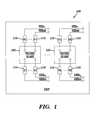
- FIG. 1is a diagram illustrating an integrated circuit chip containing voltage islands, according to the present invention
- FIG. 2is a schematic diagram of the VDD portion of a power distribution network of integrated circuit chip 100 of FIG. 1, according to the present invention
- FIG. 3is a schematic diagram of the GNDx portion of the power distribution network of integrated circuit chip 100 of FIG. 1, according to the present invention
- FIG. 4is a schematic diagram illustrating a portion of the VDDx power distribution network, 115 of FIG. 2, modeled as a resistive network, according to the present invention
- FIG. 5Ais a representative voltage-island portion of the power distribution network, 115 of FIG. 2, according to the present invention.
- FIG. 5Bis a representative model for calculating VTI current requirements, according to the present invention.
- FIG. 6Ais the chip-level portion of power distribution network, 120 of FIG. 2, chip-level placed circuits 125 , and VTI circuits 110 , according to the present invention
- FIG. 6Bis a representative model for calculating port voltages of chip-level placed circuits 125 and input voltages of VTI circuits 110 from chip-level power distribution network 120 of FIG. 6A;
- FIG. 7illustrates the calculation of VTI output voltages, according to the present invention.
- FIG. 8illustrates the current-voltage (I-V) characteristic of a typical VTI circuit
- FIGS. 9A and 9Bare flowcharts illustrating the method of analyzing integrated circuit power distribution networks in chips containing voltage islands and VTI circuits, according to the present invention.
- FIG. 10is a schematic block diagram of a general-purpose computer for practicing the present invention.
- FIG. 1is a diagram illustrating an integrated circuit chip containing voltage islands according to the present invention.
- integrated circuit chip 100includes one or more voltage island(s) 105 .
- Each voltage island 105is connected to the chip-level power distribution through one or more voltage translation interface (VTI) circuits 110 .
- VTIvoltage translation interface
- VDDxis defined as any externally-supplied chip-level power supply voltage whose relative level is more positive than its corresponding GNDx chip-level supply.
- GNDxis defined any externally-applied, chip-level power supply voltage whose relative level is more negative than its corresponding VDDx chip-level supply.
- VTI circuit 110 port voltagesare denoted VDDx 1 -VDDx m and GNDx 1 -GNDx k , where m is the number of voltage-island VDDx ports and k is the number of voltage-island GNDx ports.
- voltage islands 105 illustrated in FIG. 1are denoted identically for VDD and GND, different voltage islands may have different quantities of both VDDx and GNDx ports.
- VDDxmay represent one of several external, chip-level VDD supplies
- each VDDx and each GNDx supplycan support multiple voltage islands 105 and any VDDx/GNDx combination can be arbitrarily assigned to any voltage island.
- FIG. 2is a schematic diagram of the VDDx portion of a power distribution network of integrated circuit chip, 100 of FIG. 1, according to the present invention.
- the GNDx portion of the networkis modeled as a single, ideal voltage source.
- a power distribution network 115includes a chip-level power distribution network 120 , connected at a first subset of network ports 127 to chip-level VDDx and GNDx placed circuits 125 .
- Chip-level placed circuits 125represent switching activity that is external to any voltage island, and excites the chip-level power distribution directly.
- Chip-level power distribution network 120is also connected, at a second subset network ports 122 , through VTI circuits 110 , to one or more voltage-island power distribution networks 130 .
- Power distribution networks 130are connected at voltage-island circuit ports 132 to voltage-island placed circuits 135 . Note that any voltage-island power distribution network 130 and its constituent voltage-island placed circuits 135 are internal to its associated voltage island 105 .
- chip-level VDDx power distribution network 120is modeled as a passive, linear RLC network.
- the present inventionalso models the voltage-island power distribution networks 130 as linear circuits.
- VTI circuits 110may represent circuits or devices with nonlinear current-voltage (I-V) characteristics.
- FIG. 3is a schematic diagram of the GNDx portion of the power distribution network of integrated circuit chip 100 of FIG. 1, according to the present invention.
- the VDDx portion of the networkis modeled as a single, ideal voltage source.
- Ground distribution network 115 Aincludes a chip-level ground distribution network 140 , connected at a first subset of network ports 142 to chip-level VDDx and GNDx placed circuits 125 .
- Chip-level ground distribution network 140is also connected, at a second subset of network ports 143 , through GNDx VTI circuits 110 A, to one or more voltage-island ground distribution networks 130 A.
- Voltage-island ground distribution networks 130 Aare connected at voltage island circuit ports 144 to voltage-island placed circuits 135 .
- the chip-level ground distribution network 140 and the voltage-island ground distribution networks 130 Aare modeled as passive, linear RLC networks.
- the GNDx VTI circuits 110 Amay represent circuits or devices with linear current-voltage (I-V) characteristics.
- FIG. 4is a schematic diagram illustrating a portion of the power distribution network 115 of FIG. 2 modeled as a resistive network, according to the present invention. Also shown is one (of possibly several) VDDx VTI circuits, and current sources which represent the switching activity of both chip-level and voltage-island placed circuits.
- power distribution network model 115 Bincludes a chip-level power distribution network 120 B, and a voltage-island power distribution network 130 B.
- the wires in the chip-level power distribution network 120 Bare modeled as resistors 145 connected between network nodes 150 .
- Wires in voltage-island power distribution network 130 Bare modeled as resistors 155 connected between network nodes 160 .
- chip-level power distribution network 120 B and voltage-island power distribution network 130 Bmay be modeled with reactive circuit elements, for example, using RC or RLC systems to represent the associated interconnect wires.
- each resistor 145 and 155is replaced with an RLC network 162 including, in this example, a resistor and linear inductor in series, and two linear capacitors which couple each network node 150 and 160 to the GNDx supply. It should be understood that the method does not constrain any passive, linear power distribution modeling to the circuit configuration or topology discussed here, and that any appropriate modifications which might be made to the network representation do not constitute a departure from the scope of the invention.
- VDDx power(i.e., current) is delivered to the voltage-island power distribution network model 130 B via VDDx VTI circuits 110 connected between nodes 150 and 160 .
- VDDx VTI circuits 110For clarity, only one VTI circuit 110 is shown to be connected between one pair of network nodes 150 and 160 , however, more than one network node 150 , VTI circuit 110 , and network node 160 combination may exist in practice.
- FIG. 4illustrates a network model capable of representing the electrical behavior of the VDDx power distribution network shown in FIG. 2 . While not shown here, the invention employs suitable and analogous network representations for each GNDx “ground” distribution system, using elements of FIG. 3 and appropriate circuit models for the chip-level and voltage-island placed circuits, 125 and 135 , respectively, chip-level ground distribution network 140 , voltage-island ground distribution network 130 A, and GNDx VTI circuits 110 A.
- the method for simulating the electrical behavior of full-chip power distributionsis an iterative method. Each voltage-island power distribution is first analyzed independently on an island-by-island basis. Subsequently, the voltage-island results are combined with the chip-level power distribution analysis. Taking care to correctly “update” the network input stimuli with the most recently computed values, and then repeating the analysis procedures, the process is iterated until converging branch current and node voltage values are obtained for the entire power distribution network 115 .
- the method for simulating the electrical behavior of full-chip power distributionsis illustrated in FIG. 9 and described below.
- FIG. 5Ais a representative voltage-island portion of the power distribution network, 115 of FIG. 2, according to the present invention.
- voltage-island power distribution network 130delivers power from VTI circuits 110 to voltage-island placed circuits 135 .
- FIG. 5Bis a representative model for calculating VTI current requirements, according to the present invention.
- voltage-island power distribution network 130 Bis connected between the outputs of VTI circuits 110 of FIG. 5 A and voltage-island current sources 135 A, which represent voltage-island placed circuits 135 of FIG. 5 A.
- the linear voltage-island power distribution network 130 BUsing (a) the linear voltage-island power distribution network 130 B, (b) the voltage values, VVTI OUT1 through VVTI OUTm , which represent the voltages at the output terminals of the VTI circuits 110 of FIG.
- VTI circuit output currentsIVTI 1 through IVTI m
- VDDx IDEALis the voltage level of the externally-applied VDDx power supply. This analysis procedure for computing the VTI circuit output currents is repeated for each voltage island.
- FIG. 6Ais the chip-level portion of power distribution network, 120 of FIG. 2, chip-level placed circuits 125 , and VTI circuits 110 , according to the present invention.
- chip-level power distribution network 120is connected to VTI circuits 110 and chip-level placed circuits 125 in order to supply VDDx power to the VTI circuits and the chip-level placed circuits.
- FIG. 6Bis a representative model for calculating port voltages of chip-level placed circuits 125 and input voltages of VTI circuits 110 from chip-level power distribution network 120 of FIG. 6 A.
- VTI circuits 110 of FIG. 6Aare represented by VTI current sources 110 A and chip-level placed circuits 125 are represented by chip-level current sources 125 A.
- the VTI circuit currents, IVTI 1 through IVTI mcalculated in the manner described above in reference to FIG.
- each voltage island 105 A illustrated in FIG. 6Bis denoted as having an identical number of VTI circuits 110 A, different voltage islands 105 A may have different quantities of VTI circuits 110 A.
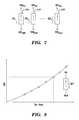
- FIG. 7illustrates the calculation of VTI output voltages, according to the present invention.
- VTI circuit current requirementsIVTI 1 through IVTI m , calculated as described above, and in reference to FIG. 5 B and (c) the modeled current-voltage (I-V) characteristic for each VTI circuit
- values for the VTI circuit output voltages, VVTI OUT1 through VVTI OUTmcan be obtained using expression evaluation, table lookup or other techniques. The exact method for “inferring” each output voltage from the corresponding current and input voltage values depends only on the manner in which the I-V characteristic is modeled and represented for use by this method.
- FIG. 8illustrates the current-voltage (I-V) characteristic of a typical VTI circuit.
- V IN -V OUTis plotted versus IVTI for a typical VTI circuit 110 .
- Vin and IVTIare known, Vout can be inferred by direct evaluation of the I-V characteristic.
- the methodis valid for both linear and nonlinear circuits. Direct evaluation of the I-V characteristic is repeated for all VTI circuits, and for each voltage island.
- FIGS. 9A and 9Bare flowcharts illustrating the method of analyzing integrated circuit power distribution networks in chips containing voltage islands and VTI circuits, according to the present invention.
- step 165chip-level power distribution network(s) 120 and chip-level ground distribution network(s) 140 are modeled as passive linear circuits.
- step 170the voltage-island power distribution network(s) 130 and the voltage-island ground distribution network(s) 130 A are modeled as passive linear circuits.
- step 175the current requirements of the chip-level placed circuits 125 and voltage-island placed circuits 135 are modeled as current sources.
- step 180a voltage of VDDx IDEAL is applied to the output ports of all VDDx VTI circuits 110 and a voltage of GNDx IDEAL is applied to the output ports of all GNDx VTI circuits 110 A.
- Thisestablishes the preliminary VTI circuit port voltages for each voltage-island power distribution network 130 (see FIG. 2) and voltage-island ground distribution network 130 A (see FIG. 3) and provides the voltage source input stimuli for initial voltage-island simulations.
- step 185the linear circuit model representing each voltage-island power distribution network 130 and voltage-island ground distribution network 130 A is simulated using the preset value (for the first iteration) or most recently computed values (for subsequent iterations) of the VTI circuit output voltages, as well as the current sources representing the corresponding voltage-island placed circuits 135 .
- step 190complete sets of network node voltages and branch currents for each voltage-island power distribution network 130 and voltage-island ground distribution network 130 A are obtained from the simulator. The method now proceeds to step 195 of FIG. 9 B.
- step 195for each voltage island 105 , the current associated with each VTI circuit 110 is obtained from the vector of measured branch current values obtained in step 190 .
- step 200the linear circuit model representing chip-level power distribution network 120 is excited using the present values of VTI circuit currents and the current sources representing the chip-level placed circuits.
- step 205complete sets of network node voltages and branch currents for the chip-level power distribution network(s) 120 and chip-level ground distribution network(s) and 140 are obtained from the simulator.
- step 210the port node voltage values corresponding to the VTI circuit inputs are extracted from the simulation results obtained in step 200 .
- step 215the VTI circuit currents obtained in step 195 , the VTI circuit input voltages obtained in step 210 , and the VTI circuit current-voltage (I-V) characteristics are used to determine the output voltage value for each VTI circuit.
- step 220the most recently determined values for the placed-circuit port voltages and all VTI circuit input and output voltages are compared to their corresponding values obtained in the previous iteration (this step is necessarily omitted in the initial iteration, where step 185 is exercised immediately after step 215 ). If the calculated node voltages deviate significantly (i.e., by more than a predetermined limit) from their previously-derived values, the analysis method is repeated, beginning at step 185 of FIG. 9A, otherwise, the loop is terminated and the network node voltages and branch currents obtained in steps 190 and 200 represent a complete solution to the VDDx/GNDx power distribution, including the networks which comprise voltage islands 105 .
- the solution time of the present inventionis dominated by simulation steps 185 and 200 of FIGS. 9A and 9B, but only for the first iteration. Since the present invention models the passive circuit elements of the VDDx and GNDx networks identically from step to step and, since only the current and voltage source values are modified, once-exercised factorization techniques can be exploited to permit extremely efficient linear system solution times for subsequent iterations.
- FIG. 10is a schematic block diagram of a general-purpose computer for practicing the present invention.
- computer system 225has at least one microprocessor or central processing unit (CPU) 230 .
- CPUcentral processing unit
- CPU 230is interconnected via a system bus 235 to a random access memory (RAM) 240 , a read-only memory (ROM) 245 , an input/output (I/O) adapter 250 for a connecting a removable data and/or program storage device 255 and a mass data and/or program storage device 260 , a user interface adapter 265 for connecting a keyboard 270 and a mouse 275 , a port adapter 280 for connecting a data port 285 and a display adapter 290 for connecting a display device 295 .
- RAMrandom access memory
- ROMread-only memory
- I/Oinput/output
- ROM 245contains the basic operating system for computer system 225 .
- the operating systemmay alternatively reside in RAM 240 or elsewhere as is known in the art.
- removable data and/or program storage device 255include magnetic media such as floppy drives and tape drives and optical media such as CD ROM drives.
- mass data and/or program storage device 250include hard disk drives and non-volatile memory such as flash memory.
- other user input devicessuch as trackballs, writing tablets, pressure pads, microphones, light pens and position-sensing screen displays may be connected to user interface 265 .
- display devicesinclude cathode-ray tubes (CRT) and liquid crystal displays (LCD).
- a computer program with an appropriate application interfacemay be created by one of skill in the art and stored on the system or a data and/or program storage device to simplify the practicing of this invention.
- information for or the computer program created to run the present inventionis loaded on the appropriate removable data and/or program storage device 255 , fed through data port 285 or typed in using keyboard 270 .
Landscapes
- Engineering & Computer Science (AREA)
- Computer Hardware Design (AREA)
- Physics & Mathematics (AREA)
- Theoretical Computer Science (AREA)
- Microelectronics & Electronic Packaging (AREA)
- Evolutionary Computation (AREA)
- Geometry (AREA)
- General Engineering & Computer Science (AREA)
- General Physics & Mathematics (AREA)
- Semiconductor Integrated Circuits (AREA)
Abstract
Description
Claims (16)
Priority Applications (1)
| Application Number | Priority Date | Filing Date | Title |
|---|---|---|---|
| US09/683,545US6631502B2 (en) | 2002-01-16 | 2002-01-16 | Method of analyzing integrated circuit power distribution in chips containing voltage islands |
Applications Claiming Priority (1)
| Application Number | Priority Date | Filing Date | Title |
|---|---|---|---|
| US09/683,545US6631502B2 (en) | 2002-01-16 | 2002-01-16 | Method of analyzing integrated circuit power distribution in chips containing voltage islands |
Publications (2)
| Publication Number | Publication Date |
|---|---|
| US20030135830A1 US20030135830A1 (en) | 2003-07-17 |
| US6631502B2true US6631502B2 (en) | 2003-10-07 |
Family
ID=24744483
Family Applications (1)
| Application Number | Title | Priority Date | Filing Date |
|---|---|---|---|
| US09/683,545Expired - LifetimeUS6631502B2 (en) | 2002-01-16 | 2002-01-16 | Method of analyzing integrated circuit power distribution in chips containing voltage islands |
Country Status (1)
| Country | Link |
|---|---|
| US (1) | US6631502B2 (en) |
Cited By (39)
| Publication number | Priority date | Publication date | Assignee | Title |
|---|---|---|---|---|
| US20030169059A1 (en)* | 2002-03-08 | 2003-09-11 | Bodenstab Paul Robert | Method and program product for evaluating a circuit |
| US20030206051A1 (en)* | 2002-05-01 | 2003-11-06 | International Business Machines Corporation | Global voltage buffer for voltage islands |
| US20030212973A1 (en)* | 2002-05-13 | 2003-11-13 | Shen Lin | Methods for full-chip vectorless dynamic IR analysis in IC designs |
| US20040268278A1 (en)* | 2003-05-07 | 2004-12-30 | Hoberman Barry Alan | Managing power on integrated circuits using power islands |
| US20050010887A1 (en)* | 2003-07-08 | 2005-01-13 | International Business Machines Corporation | Nested voltage island architecture |
| US20050203722A1 (en)* | 2004-03-13 | 2005-09-15 | Jong-Eun Koo | Power distribution network simulation method using variable reduction method |
| US20050278676A1 (en)* | 2004-05-25 | 2005-12-15 | Dhanwada Nagashyamala R | Method of physical planning voltage islands for ASICs and system-on-chip designs |
| US20060090147A1 (en)* | 2004-10-19 | 2006-04-27 | Sharp Kabushiki Kaisha | Inspection method and inspection apparatus for semiconductor integrated circuit |
| US20060259840A1 (en)* | 2005-05-12 | 2006-11-16 | International Business Machines Corporation | Self-test circuitry to determine minimum operating voltage |
| US20060265681A1 (en)* | 2005-05-19 | 2006-11-23 | International Business Machines Corporation | An automated and electrically robust method for placing power gating switches in voltage islands |
| US20070176639A1 (en)* | 2004-02-19 | 2007-08-02 | Mosaid Delaware, Inc. | Low leakage and data retention circuitry |
| US7277841B1 (en)* | 2002-02-11 | 2007-10-02 | Sun Microsystems, Inc. | Method for adaptive sub-gridding for power/ground plane simulations |
| US20070230082A1 (en)* | 2006-03-30 | 2007-10-04 | Peter Poechmueller | Integrated circuit having a plurality of externally fed power supply systems |
| US20070247236A1 (en)* | 2006-04-06 | 2007-10-25 | Mosaid Technologies Corporation | Phase-locked loop filter capacitance with a drag current |
| US20080007323A1 (en)* | 2004-07-09 | 2008-01-10 | Mosaid Technologies Corporation | Systems and methods forminimizing static leakage of an integrated circuit |
| US20080024197A1 (en)* | 2006-03-31 | 2008-01-31 | Kerry Bernstein | Method and architecture for power management of an electronic device |
| US20080030254A1 (en)* | 2006-08-02 | 2008-02-07 | Igor Arsovski | Design structure to eliminate step response power supply perturbation |
| US20080030223A1 (en)* | 2006-08-02 | 2008-02-07 | Igor Arsovski | Device and method to eliminate step response power supply perturbation |
| US7345944B1 (en) | 2006-01-11 | 2008-03-18 | Xilinx, Inc. | Programmable detection of power failure in an integrated circuit |
| US20080098340A1 (en)* | 2004-12-06 | 2008-04-24 | Entasys Design, Inc. | Method for Designing Block Placement and Power Distribution of Semiconductor Integrated Circuit |
| US20080211570A1 (en)* | 2006-12-31 | 2008-09-04 | Sandisk Corporation | Systems, Methods, and Integrated Circuits with Inrush-Limited Power Islands |
| US20080281574A1 (en)* | 2007-05-07 | 2008-11-13 | Ryan Bazinet | System and method for glitch analysis in circuits |
| US20080297961A1 (en)* | 2006-12-31 | 2008-12-04 | Sandisk Corporation | Systems, Circuits, Chips and Methods with Protection at Power Island Boundaries |
| US7498835B1 (en) | 2005-11-04 | 2009-03-03 | Xilinx, Inc. | Implementation of low power standby modes for integrated circuits |
| US7498836B1 (en) | 2003-09-19 | 2009-03-03 | Xilinx, Inc. | Programmable low power modes for embedded memory blocks |
| US7498839B1 (en) | 2004-10-22 | 2009-03-03 | Xilinx, Inc. | Low power zones for programmable logic devices |
| US7504854B1 (en) | 2003-09-19 | 2009-03-17 | Xilinx, Inc. | Regulating unused/inactive resources in programmable logic devices for static power reduction |
| US7549139B1 (en) | 2003-09-19 | 2009-06-16 | Xilinx, Inc. | Tuning programmable logic devices for low-power design implementation |
| US7562332B1 (en) | 2003-09-19 | 2009-07-14 | Xilinx, Inc. | Disabling unused/inactive resources in programmable logic devices for static power reduction |
| US7581124B1 (en) | 2003-09-19 | 2009-08-25 | Xilinx, Inc. | Method and mechanism for controlling power consumption of an integrated circuit |
| US7770142B1 (en)* | 2006-10-30 | 2010-08-03 | Cadence Design Systems, Inc. | Modeling power management for an integrated circuit |
| US20110082682A1 (en)* | 2009-10-03 | 2011-04-07 | Raytheon Company | Systems power distribution tool |
| US8176212B1 (en)* | 2009-08-18 | 2012-05-08 | Quickflex, Inc. | Method and system for hierarchical and joinable behavior containers for reconfigurable computing |
| US20120198408A1 (en)* | 2011-01-31 | 2012-08-02 | Amit Chopra | System and method for automatic extraction of power intent from custom analog/custom digital/mixed signal schematic designs |
| CN103077278A (en)* | 2013-01-06 | 2013-05-01 | 宁波大学 | Distribution method for power supply pins of voltage island in system on chip (SOC) |
| US8823405B1 (en) | 2010-09-10 | 2014-09-02 | Xilinx, Inc. | Integrated circuit with power gating |
| US20150070048A1 (en)* | 2013-09-06 | 2015-03-12 | International Business Machines Corporation | Verifying partial good voltage island structures |
| US9419624B2 (en) | 2014-11-12 | 2016-08-16 | Xilinx, Inc. | Power management system for integrated circuits |
| US20190148284A1 (en)* | 2017-11-16 | 2019-05-16 | International Business Machines Corporation | Managed integrated circuit power supply distribution |
Families Citing this family (7)
| Publication number | Priority date | Publication date | Assignee | Title |
|---|---|---|---|---|
| US7275164B2 (en)* | 2005-01-31 | 2007-09-25 | International Business Machines Corporation | System and method for fencing any one of the plurality of voltage islands using a lookup table including AC and DC components for each functional block of the voltage islands |
| US7574683B2 (en)* | 2005-08-05 | 2009-08-11 | John Wilson | Automating power domains in electronic design automation |
| US7830039B2 (en)* | 2007-12-28 | 2010-11-09 | Sandisk Corporation | Systems and circuits with multirange and localized detection of valid power |
| US8516423B2 (en)* | 2009-09-29 | 2013-08-20 | Nanotropic S.A. | System and method for determining simulated response extrema for integrated circuit power supply networks |
| KR101861743B1 (en)* | 2011-09-19 | 2018-05-30 | 삼성전자주식회사 | System-on chip for selectively performing heterogeneous power control and homegeneous power control, and method thereof |
| KR102276908B1 (en)* | 2014-12-05 | 2021-07-13 | 삼성전자주식회사 | A computing device executable for a program performing a method for analysing power noise in a semiconductor device, a method including the same for designing a semiconductor device, and a program strorage medium storing the program |
| US9824174B2 (en)* | 2015-09-11 | 2017-11-21 | Qualcomm Incorporated | Power-density-based clock cell spacing |
Citations (6)
| Publication number | Priority date | Publication date | Assignee | Title |
|---|---|---|---|---|
| US4451743A (en)* | 1980-12-29 | 1984-05-29 | Citizen Watch Company Limited | DC-to-DC Voltage converter |
| US5672997A (en)* | 1994-09-21 | 1997-09-30 | Intel Corporation | Method and apparatus for reducing the nominal operating voltage supplied to an integrated circuit |
| US6181027B1 (en)* | 1999-02-26 | 2001-01-30 | International Business Machine Corp. | DC power distribution |
| US20020038732A1 (en)* | 2000-10-04 | 2002-04-04 | Toyota Jidosha Kabushiki Kaisha | DC power supply using fuel cell |
| US20020149263A1 (en)* | 2001-04-11 | 2002-10-17 | International Business Machines Corporation | Voltage island fencing |
| US6493859B1 (en)* | 2001-10-01 | 2002-12-10 | International Business Machines Corporation | Method of wiring power service terminals to a power network in a semiconductor integrated circuit |
- 2002
- 2002-01-16USUS09/683,545patent/US6631502B2/ennot_activeExpired - Lifetime
Patent Citations (6)
| Publication number | Priority date | Publication date | Assignee | Title |
|---|---|---|---|---|
| US4451743A (en)* | 1980-12-29 | 1984-05-29 | Citizen Watch Company Limited | DC-to-DC Voltage converter |
| US5672997A (en)* | 1994-09-21 | 1997-09-30 | Intel Corporation | Method and apparatus for reducing the nominal operating voltage supplied to an integrated circuit |
| US6181027B1 (en)* | 1999-02-26 | 2001-01-30 | International Business Machine Corp. | DC power distribution |
| US20020038732A1 (en)* | 2000-10-04 | 2002-04-04 | Toyota Jidosha Kabushiki Kaisha | DC power supply using fuel cell |
| US20020149263A1 (en)* | 2001-04-11 | 2002-10-17 | International Business Machines Corporation | Voltage island fencing |
| US6493859B1 (en)* | 2001-10-01 | 2002-12-10 | International Business Machines Corporation | Method of wiring power service terminals to a power network in a semiconductor integrated circuit |
Non-Patent Citations (1)
| Title |
|---|
| MAXIM, New Release Data Book (1995), vol. IV, Maxim Integrated Products, Inc. pp 4-47 to 4-56.* |
Cited By (88)
| Publication number | Priority date | Publication date | Assignee | Title |
|---|---|---|---|---|
| US7277841B1 (en)* | 2002-02-11 | 2007-10-02 | Sun Microsystems, Inc. | Method for adaptive sub-gridding for power/ground plane simulations |
| US6856148B2 (en)* | 2002-03-08 | 2005-02-15 | Hewlett-Packard Development Company, L.P. | Method and program product for evaluating a circuit |
| US20030169059A1 (en)* | 2002-03-08 | 2003-09-11 | Bodenstab Paul Robert | Method and program product for evaluating a circuit |
| US20030206051A1 (en)* | 2002-05-01 | 2003-11-06 | International Business Machines Corporation | Global voltage buffer for voltage islands |
| US6731154B2 (en)* | 2002-05-01 | 2004-05-04 | International Business Machines Corporation | Global voltage buffer for voltage islands |
| US20030212973A1 (en)* | 2002-05-13 | 2003-11-13 | Shen Lin | Methods for full-chip vectorless dynamic IR analysis in IC designs |
| US7996811B2 (en) | 2003-05-07 | 2011-08-09 | Mosaid Technologies Incorporated | Power managers for an integrated circuit |
| US7415680B2 (en)* | 2003-05-07 | 2008-08-19 | Mosaid Technologies Corporation | Power managers for an integrated circuit |
| EP1623349B1 (en) | 2003-05-07 | 2018-01-24 | Conversant Intellectual Property Management Inc. | Managing power on integrated circuits using power islands |
| US8782590B2 (en) | 2003-05-07 | 2014-07-15 | Conversant Intellectual Property Management Inc. | Power managers for an integrated circuit |
| US8762923B2 (en) | 2003-05-07 | 2014-06-24 | Conversant Intellectual Property Management Inc. | Power managers for an integrated circuit |
| US7051306B2 (en)* | 2003-05-07 | 2006-05-23 | Mosaid Technologies Corporation | Managing power on integrated circuits using power islands |
| US20060123365A1 (en)* | 2003-05-07 | 2006-06-08 | Hoberman Barry A | Power managers for an integrated circuit |
| US20080276105A1 (en)* | 2003-05-07 | 2008-11-06 | Mosaid Technologies Corporation | Power managers for an integrated circuit |
| US20090152948A1 (en)* | 2003-05-07 | 2009-06-18 | Mosaid Technologies Corporation | Power managers for an integrated circuit |
| WO2004102623A3 (en)* | 2003-05-07 | 2005-07-14 | Virtual Silicon Technology Inc | Managing power on integrated circuits using power islands |
| KR101053010B1 (en)* | 2003-05-07 | 2011-07-29 | 모사이드 테크놀로지스, 인코포레이티드 | Managing power on integrated circuits using power islands |
| US7945885B2 (en) | 2003-05-07 | 2011-05-17 | Mosaid Technologies Incorporated | Power managers for an integrated circuit |
| US20040268278A1 (en)* | 2003-05-07 | 2004-12-30 | Hoberman Barry Alan | Managing power on integrated circuits using power islands |
| KR100992177B1 (en) | 2003-05-07 | 2010-11-04 | 모사이드 테크놀로지스 코포레이션 | Managing power on integrated circuits using power islands |
| KR100915258B1 (en)* | 2003-05-07 | 2009-09-03 | 모사이드 테크놀로지스 코포레이션 | Managing power on integrated circuits using power islands |
| US20050010887A1 (en)* | 2003-07-08 | 2005-01-13 | International Business Machines Corporation | Nested voltage island architecture |
| US7131074B2 (en)* | 2003-07-08 | 2006-10-31 | International Business Machines Corporation | Nested voltage island architecture |
| US8099691B1 (en) | 2003-09-19 | 2012-01-17 | Xilinx, Inc. | Disabling unused/inactive resources in an integrated circuit for static power reduction |
| US7581124B1 (en) | 2003-09-19 | 2009-08-25 | Xilinx, Inc. | Method and mechanism for controlling power consumption of an integrated circuit |
| US7498836B1 (en) | 2003-09-19 | 2009-03-03 | Xilinx, Inc. | Programmable low power modes for embedded memory blocks |
| US7549139B1 (en) | 2003-09-19 | 2009-06-16 | Xilinx, Inc. | Tuning programmable logic devices for low-power design implementation |
| US7562332B1 (en) | 2003-09-19 | 2009-07-14 | Xilinx, Inc. | Disabling unused/inactive resources in programmable logic devices for static power reduction |
| US7504854B1 (en) | 2003-09-19 | 2009-03-17 | Xilinx, Inc. | Regulating unused/inactive resources in programmable logic devices for static power reduction |
| US7940081B2 (en) | 2004-02-19 | 2011-05-10 | Mosaid Technologies Incorporated | Low leakage and data retention circuitry |
| US20100060319A1 (en)* | 2004-02-19 | 2010-03-11 | Mosaid Technologies Corporation | Low leakage and data retention circuitry |
| US7592837B2 (en) | 2004-02-19 | 2009-09-22 | Mosaid Technologies Corporation | Low leakage and data retention circuitry |
| US7348804B2 (en) | 2004-02-19 | 2008-03-25 | Mosaid Delaware, Inc. | Low leakage and data retention circuitry |
| US8854077B2 (en) | 2004-02-19 | 2014-10-07 | Conversant Intellectual Property Management Inc. | Low leakage and data retention circuitry |
| US20090027080A1 (en)* | 2004-02-19 | 2009-01-29 | Mosaid Technologies, Inc. | Low leakage and data retention circuitry |
| US8253438B2 (en) | 2004-02-19 | 2012-08-28 | Mosaid Technologies Incorporated | Low leakage and data retention circuitry |
| US20070176639A1 (en)* | 2004-02-19 | 2007-08-02 | Mosaid Delaware, Inc. | Low leakage and data retention circuitry |
| US20050203722A1 (en)* | 2004-03-13 | 2005-09-15 | Jong-Eun Koo | Power distribution network simulation method using variable reduction method |
| US7509596B2 (en) | 2004-03-13 | 2009-03-24 | Samsung Electronics Co, Ltd. | Power distribution network simulation method using variable reduction method |
| US20050278676A1 (en)* | 2004-05-25 | 2005-12-15 | Dhanwada Nagashyamala R | Method of physical planning voltage islands for ASICs and system-on-chip designs |
| US7296251B2 (en)* | 2004-05-25 | 2007-11-13 | International Business Machines Corporation | Method of physical planning voltage islands for ASICs and system-on-chip designs |
| US20080007323A1 (en)* | 2004-07-09 | 2008-01-10 | Mosaid Technologies Corporation | Systems and methods forminimizing static leakage of an integrated circuit |
| US7642836B2 (en) | 2004-07-09 | 2010-01-05 | Mosaid Technologies Incorporated | Systems and methods for minimizing static leakage of an integrated circuit |
| US20080088358A1 (en)* | 2004-07-09 | 2008-04-17 | Mosaid Technologies Corporation | Systems and methods for minimizing static leakage of an integrated circuit |
| US20100066439A1 (en)* | 2004-07-09 | 2010-03-18 | Mosaid Technologies Incorporated | Systems and methods for minimizing static leakage of an integrated circuit |
| US7382178B2 (en) | 2004-07-09 | 2008-06-03 | Mosaid Technologies Corporation | Systems and methods for minimizing static leakage of an integrated circuit |
| USRE49854E1 (en) | 2004-07-09 | 2024-02-27 | Mosaid Technologies Incorporated | Systems and methods for minimizing static leakage of an integrated circuit |
| US7982532B2 (en) | 2004-07-09 | 2011-07-19 | Mosaid Technologies Incorporated | Systems and methods for minimizing static leakage of an integrated circuit |
| US7404158B2 (en)* | 2004-10-19 | 2008-07-22 | Sharp Kabushiki Kaisha | Inspection method and inspection apparatus for semiconductor integrated circuit |
| US20060090147A1 (en)* | 2004-10-19 | 2006-04-27 | Sharp Kabushiki Kaisha | Inspection method and inspection apparatus for semiconductor integrated circuit |
| US7498839B1 (en) | 2004-10-22 | 2009-03-03 | Xilinx, Inc. | Low power zones for programmable logic devices |
| US20080098340A1 (en)* | 2004-12-06 | 2008-04-24 | Entasys Design, Inc. | Method for Designing Block Placement and Power Distribution of Semiconductor Integrated Circuit |
| US20060259840A1 (en)* | 2005-05-12 | 2006-11-16 | International Business Machines Corporation | Self-test circuitry to determine minimum operating voltage |
| US7266797B2 (en) | 2005-05-19 | 2007-09-04 | International Business Machines Corporation | Automated and electrically robust method for placing power gating switches in voltage islands |
| US20060265681A1 (en)* | 2005-05-19 | 2006-11-23 | International Business Machines Corporation | An automated and electrically robust method for placing power gating switches in voltage islands |
| US7498835B1 (en) | 2005-11-04 | 2009-03-03 | Xilinx, Inc. | Implementation of low power standby modes for integrated circuits |
| US7345944B1 (en) | 2006-01-11 | 2008-03-18 | Xilinx, Inc. | Programmable detection of power failure in an integrated circuit |
| US20070230082A1 (en)* | 2006-03-30 | 2007-10-04 | Peter Poechmueller | Integrated circuit having a plurality of externally fed power supply systems |
| US20080024197A1 (en)* | 2006-03-31 | 2008-01-31 | Kerry Bernstein | Method and architecture for power management of an electronic device |
| US7831935B2 (en)* | 2006-03-31 | 2010-11-09 | International Business Machines Corporation | Method and architecture for power management of an electronic device |
| US20070247236A1 (en)* | 2006-04-06 | 2007-10-25 | Mosaid Technologies Corporation | Phase-locked loop filter capacitance with a drag current |
| US7567133B2 (en) | 2006-04-06 | 2009-07-28 | Mosaid Technologies Corporation | Phase-locked loop filter capacitance with a drag current |
| US20080030254A1 (en)* | 2006-08-02 | 2008-02-07 | Igor Arsovski | Design structure to eliminate step response power supply perturbation |
| US7705626B2 (en)* | 2006-08-02 | 2010-04-27 | International Business Machines Corporation | Design structure to eliminate step response power supply perturbation |
| US20080030223A1 (en)* | 2006-08-02 | 2008-02-07 | Igor Arsovski | Device and method to eliminate step response power supply perturbation |
| US7511528B2 (en)* | 2006-08-02 | 2009-03-31 | International Business Machines Corporation | Device and method to eliminate step response power supply perturbation |
| US7770142B1 (en)* | 2006-10-30 | 2010-08-03 | Cadence Design Systems, Inc. | Modeling power management for an integrated circuit |
| US7948264B2 (en)* | 2006-12-31 | 2011-05-24 | Sandisk Corporation | Systems, methods, and integrated circuits with inrush-limited power islands |
| US20080211570A1 (en)* | 2006-12-31 | 2008-09-04 | Sandisk Corporation | Systems, Methods, and Integrated Circuits with Inrush-Limited Power Islands |
| US8072719B2 (en) | 2006-12-31 | 2011-12-06 | Sandisk Technologies Inc. | Systems, circuits, chips and methods with protection at power island boundaries |
| US20080297961A1 (en)* | 2006-12-31 | 2008-12-04 | Sandisk Corporation | Systems, Circuits, Chips and Methods with Protection at Power Island Boundaries |
| US20080281574A1 (en)* | 2007-05-07 | 2008-11-13 | Ryan Bazinet | System and method for glitch analysis in circuits |
| US7809542B2 (en) | 2007-05-07 | 2010-10-05 | International Business Machines Corporation | System and method for glitch analysis in circuits |
| US8176212B1 (en)* | 2009-08-18 | 2012-05-08 | Quickflex, Inc. | Method and system for hierarchical and joinable behavior containers for reconfigurable computing |
| US20110082682A1 (en)* | 2009-10-03 | 2011-04-07 | Raytheon Company | Systems power distribution tool |
| US8195437B2 (en) | 2009-10-03 | 2012-06-05 | Raytheon Company | Systems power distribution tool |
| US8823405B1 (en) | 2010-09-10 | 2014-09-02 | Xilinx, Inc. | Integrated circuit with power gating |
| US8407635B2 (en)* | 2011-01-31 | 2013-03-26 | Cadence Design Systems, Inc. | System and method for automatic extraction of power intent from custom analog/custom digital/mixed signal schematic designs |
| US20120198408A1 (en)* | 2011-01-31 | 2012-08-02 | Amit Chopra | System and method for automatic extraction of power intent from custom analog/custom digital/mixed signal schematic designs |
| CN103077278B (en)* | 2013-01-06 | 2015-11-18 | 宁波大学 | A kind of voltage island energization pins distribution method of SOC (system on a chip) |
| CN103077278A (en)* | 2013-01-06 | 2013-05-01 | 宁波大学 | Distribution method for power supply pins of voltage island in system on chip (SOC) |
| US9172373B2 (en)* | 2013-09-06 | 2015-10-27 | Globalfoundries U.S. 2 Llc | Verifying partial good voltage island structures |
| US20150070048A1 (en)* | 2013-09-06 | 2015-03-12 | International Business Machines Corporation | Verifying partial good voltage island structures |
| US9419624B2 (en) | 2014-11-12 | 2016-08-16 | Xilinx, Inc. | Power management system for integrated circuits |
| US20190148284A1 (en)* | 2017-11-16 | 2019-05-16 | International Business Machines Corporation | Managed integrated circuit power supply distribution |
| US20190348361A1 (en)* | 2017-11-16 | 2019-11-14 | International Business Machines Corporation | Managed integrated circuit power supply distribution |
| US10580730B2 (en)* | 2017-11-16 | 2020-03-03 | International Business Machines Corporation | Managed integrated circuit power supply distribution |
| US11018084B2 (en)* | 2017-11-16 | 2021-05-25 | International Business Machines Corporation | Managed integrated circuit power supply distribution |
Also Published As
| Publication number | Publication date |
|---|---|
| US20030135830A1 (en) | 2003-07-17 |
Similar Documents
| Publication | Publication Date | Title |
|---|---|---|
| US6631502B2 (en) | Method of analyzing integrated circuit power distribution in chips containing voltage islands | |
| US11574105B1 (en) | Using a barycenter compact model for a circuit network | |
| US8381151B1 (en) | Method and system for power distribution analysis | |
| US7627844B2 (en) | Methods and apparatuses for transient analyses of circuits | |
| JP6893232B2 (en) | Computer-implemented method and recording medium for translation of electronic design verification commands | |
| US11657201B2 (en) | Computer implemented system and method of identification of useful untested states of an electronic design | |
| US7933747B2 (en) | Method and system for simulating dynamic behavior of a transistor | |
| US11681854B2 (en) | Generation of layout including power delivery network | |
| US20060048081A1 (en) | System and method for modeling an integrated circuit system | |
| US8595677B1 (en) | Method and system for performing voltage-based fast electrical analysis and simulation of an electronic design | |
| US20210357539A1 (en) | Computer implemented system and method of translation of verification commands of an electronic design | |
| US7987439B2 (en) | Method and apparatus for analyzing circuit model by reduction and computer program product for analyzing the circuit model | |
| US9471733B1 (en) | Solving a circuit network in multicore or distributed computing environment | |
| US7373289B2 (en) | Electrical isomorphism | |
| JPH06317631A (en) | Method for developing test plan for analog integrated circuit | |
| Novichkova et al. | Approach to Integration of a Synthesis Tool and PDK for Commercial EDA | |
| JP4233513B2 (en) | Analysis device, analysis program, and computer-readable recording medium recording analysis program | |
| JP2005071370A (en) | System and method for determining activity factor for circuit design | |
| JPH07287051A (en) | Input data generator for logic simulator | |
| JP3851771B2 (en) | Voltage drop analysis system | |
| US11100268B1 (en) | Fast and accurate simulation for power delivery networks with integrated voltage regulators | |
| JP2940467B2 (en) | Output load capacity calculation method | |
| Conti et al. | An integrated CAD methodology for yield enhancement of VLSI CMOS circuits including statistical device variations | |
| Denk et al. | Circuit simulation for nanoelectronics | |
| JPH04241068A (en) | Circuit simulation system |
Legal Events
| Date | Code | Title | Description |
|---|---|---|---|
| AS | Assignment | Owner name:INTERNATIONAL BUSINESS MACHINES CORPORATION, NEW Y Free format text:ASSIGNMENT OF ASSIGNORS INTEREST;ASSIGNORS:BUFFET, PATRICK H.;KOZHAYA, JOSEPH N.;MONTANE, PAUL D.;AND OTHERS;REEL/FRAME:012311/0117;SIGNING DATES FROM 20011212 TO 20011221 | |
| STCF | Information on status: patent grant | Free format text:PATENTED CASE | |
| FEPP | Fee payment procedure | Free format text:PAYOR NUMBER ASSIGNED (ORIGINAL EVENT CODE: ASPN); ENTITY STATUS OF PATENT OWNER: LARGE ENTITY | |
| FPAY | Fee payment | Year of fee payment:4 | |
| REMI | Maintenance fee reminder mailed | ||
| FPAY | Fee payment | Year of fee payment:8 | |
| SULP | Surcharge for late payment | Year of fee payment:7 | |
| AS | Assignment | Owner name:GOOGLE INC., CALIFORNIA Free format text:ASSIGNMENT OF ASSIGNORS INTEREST;ASSIGNOR:INTERNATIONAL BUSINESS MACHINES CORPORATION;REEL/FRAME:026664/0866 Effective date:20110503 | |
| FPAY | Fee payment | Year of fee payment:12 | |
| AS | Assignment | Owner name:GOOGLE LLC, CALIFORNIA Free format text:CHANGE OF NAME;ASSIGNOR:GOOGLE INC.;REEL/FRAME:044127/0735 Effective date:20170929 |