US6630916B1 - Method and a circuit for gradationally driving a flat display device - Google Patents
Method and a circuit for gradationally driving a flat display deviceDownload PDFInfo
- Publication number
- US6630916B1 US6630916B1US09/451,351US45135199AUS6630916B1US 6630916 B1US6630916 B1US 6630916B1US 45135199 AUS45135199 AUS 45135199AUS 6630916 B1US6630916 B1US 6630916B1
- Authority
- US
- United States
- Prior art keywords
- period
- cells
- subframe
- subframes
- display panel
- Prior art date
- Legal status (The legal status is an assumption and is not a legal conclusion. Google has not performed a legal analysis and makes no representation as to the accuracy of the status listed.)
- Expired - Fee Related
Links
Images


Classifications
- G—PHYSICS
- G09—EDUCATION; CRYPTOGRAPHY; DISPLAY; ADVERTISING; SEALS
- G09G—ARRANGEMENTS OR CIRCUITS FOR CONTROL OF INDICATING DEVICES USING STATIC MEANS TO PRESENT VARIABLE INFORMATION
- G09G3/00—Control arrangements or circuits, of interest only in connection with visual indicators other than cathode-ray tubes
- G09G3/20—Control arrangements or circuits, of interest only in connection with visual indicators other than cathode-ray tubes for presentation of an assembly of a number of characters, e.g. a page, by composing the assembly by combination of individual elements arranged in a matrix no fixed position being assigned to or needed to be assigned to the individual characters or partial characters
- G09G3/22—Control arrangements or circuits, of interest only in connection with visual indicators other than cathode-ray tubes for presentation of an assembly of a number of characters, e.g. a page, by composing the assembly by combination of individual elements arranged in a matrix no fixed position being assigned to or needed to be assigned to the individual characters or partial characters using controlled light sources
- G09G3/28—Control arrangements or circuits, of interest only in connection with visual indicators other than cathode-ray tubes for presentation of an assembly of a number of characters, e.g. a page, by composing the assembly by combination of individual elements arranged in a matrix no fixed position being assigned to or needed to be assigned to the individual characters or partial characters using controlled light sources using luminous gas-discharge panels, e.g. plasma panels
- G09G3/288—Control arrangements or circuits, of interest only in connection with visual indicators other than cathode-ray tubes for presentation of an assembly of a number of characters, e.g. a page, by composing the assembly by combination of individual elements arranged in a matrix no fixed position being assigned to or needed to be assigned to the individual characters or partial characters using controlled light sources using luminous gas-discharge panels, e.g. plasma panels using AC panels
- G09G3/291—Control arrangements or circuits, of interest only in connection with visual indicators other than cathode-ray tubes for presentation of an assembly of a number of characters, e.g. a page, by composing the assembly by combination of individual elements arranged in a matrix no fixed position being assigned to or needed to be assigned to the individual characters or partial characters using controlled light sources using luminous gas-discharge panels, e.g. plasma panels using AC panels controlling the gas discharge to control a cell condition, e.g. by means of specific pulse shapes
- G09G3/294—Control arrangements or circuits, of interest only in connection with visual indicators other than cathode-ray tubes for presentation of an assembly of a number of characters, e.g. a page, by composing the assembly by combination of individual elements arranged in a matrix no fixed position being assigned to or needed to be assigned to the individual characters or partial characters using controlled light sources using luminous gas-discharge panels, e.g. plasma panels using AC panels controlling the gas discharge to control a cell condition, e.g. by means of specific pulse shapes for lighting or sustain discharge
- G—PHYSICS
- G09—EDUCATION; CRYPTOGRAPHY; DISPLAY; ADVERTISING; SEALS
- G09G—ARRANGEMENTS OR CIRCUITS FOR CONTROL OF INDICATING DEVICES USING STATIC MEANS TO PRESENT VARIABLE INFORMATION
- G09G3/00—Control arrangements or circuits, of interest only in connection with visual indicators other than cathode-ray tubes
- G09G3/20—Control arrangements or circuits, of interest only in connection with visual indicators other than cathode-ray tubes for presentation of an assembly of a number of characters, e.g. a page, by composing the assembly by combination of individual elements arranged in a matrix no fixed position being assigned to or needed to be assigned to the individual characters or partial characters
- G09G3/2003—Display of colours
- G—PHYSICS
- G09—EDUCATION; CRYPTOGRAPHY; DISPLAY; ADVERTISING; SEALS
- G09G—ARRANGEMENTS OR CIRCUITS FOR CONTROL OF INDICATING DEVICES USING STATIC MEANS TO PRESENT VARIABLE INFORMATION
- G09G3/00—Control arrangements or circuits, of interest only in connection with visual indicators other than cathode-ray tubes
- G09G3/20—Control arrangements or circuits, of interest only in connection with visual indicators other than cathode-ray tubes for presentation of an assembly of a number of characters, e.g. a page, by composing the assembly by combination of individual elements arranged in a matrix no fixed position being assigned to or needed to be assigned to the individual characters or partial characters
- G09G3/2007—Display of intermediate tones
- G09G3/2018—Display of intermediate tones by time modulation using two or more time intervals
- G09G3/2022—Display of intermediate tones by time modulation using two or more time intervals using sub-frames
- G09G3/2025—Display of intermediate tones by time modulation using two or more time intervals using sub-frames the sub-frames having all the same time duration
- G—PHYSICS
- G09—EDUCATION; CRYPTOGRAPHY; DISPLAY; ADVERTISING; SEALS
- G09G—ARRANGEMENTS OR CIRCUITS FOR CONTROL OF INDICATING DEVICES USING STATIC MEANS TO PRESENT VARIABLE INFORMATION
- G09G3/00—Control arrangements or circuits, of interest only in connection with visual indicators other than cathode-ray tubes
- G09G3/20—Control arrangements or circuits, of interest only in connection with visual indicators other than cathode-ray tubes for presentation of an assembly of a number of characters, e.g. a page, by composing the assembly by combination of individual elements arranged in a matrix no fixed position being assigned to or needed to be assigned to the individual characters or partial characters
- G09G3/22—Control arrangements or circuits, of interest only in connection with visual indicators other than cathode-ray tubes for presentation of an assembly of a number of characters, e.g. a page, by composing the assembly by combination of individual elements arranged in a matrix no fixed position being assigned to or needed to be assigned to the individual characters or partial characters using controlled light sources
- G09G3/28—Control arrangements or circuits, of interest only in connection with visual indicators other than cathode-ray tubes for presentation of an assembly of a number of characters, e.g. a page, by composing the assembly by combination of individual elements arranged in a matrix no fixed position being assigned to or needed to be assigned to the individual characters or partial characters using controlled light sources using luminous gas-discharge panels, e.g. plasma panels
- G09G3/288—Control arrangements or circuits, of interest only in connection with visual indicators other than cathode-ray tubes for presentation of an assembly of a number of characters, e.g. a page, by composing the assembly by combination of individual elements arranged in a matrix no fixed position being assigned to or needed to be assigned to the individual characters or partial characters using controlled light sources using luminous gas-discharge panels, e.g. plasma panels using AC panels
- G09G3/291—Control arrangements or circuits, of interest only in connection with visual indicators other than cathode-ray tubes for presentation of an assembly of a number of characters, e.g. a page, by composing the assembly by combination of individual elements arranged in a matrix no fixed position being assigned to or needed to be assigned to the individual characters or partial characters using controlled light sources using luminous gas-discharge panels, e.g. plasma panels using AC panels controlling the gas discharge to control a cell condition, e.g. by means of specific pulse shapes
- G09G3/292—Control arrangements or circuits, of interest only in connection with visual indicators other than cathode-ray tubes for presentation of an assembly of a number of characters, e.g. a page, by composing the assembly by combination of individual elements arranged in a matrix no fixed position being assigned to or needed to be assigned to the individual characters or partial characters using controlled light sources using luminous gas-discharge panels, e.g. plasma panels using AC panels controlling the gas discharge to control a cell condition, e.g. by means of specific pulse shapes for reset discharge, priming discharge or erase discharge occurring in a phase other than addressing
- G09G3/2927—Details of initialising
- G—PHYSICS
- G09—EDUCATION; CRYPTOGRAPHY; DISPLAY; ADVERTISING; SEALS
- G09G—ARRANGEMENTS OR CIRCUITS FOR CONTROL OF INDICATING DEVICES USING STATIC MEANS TO PRESENT VARIABLE INFORMATION
- G09G3/00—Control arrangements or circuits, of interest only in connection with visual indicators other than cathode-ray tubes
- G09G3/20—Control arrangements or circuits, of interest only in connection with visual indicators other than cathode-ray tubes for presentation of an assembly of a number of characters, e.g. a page, by composing the assembly by combination of individual elements arranged in a matrix no fixed position being assigned to or needed to be assigned to the individual characters or partial characters
- G09G3/22—Control arrangements or circuits, of interest only in connection with visual indicators other than cathode-ray tubes for presentation of an assembly of a number of characters, e.g. a page, by composing the assembly by combination of individual elements arranged in a matrix no fixed position being assigned to or needed to be assigned to the individual characters or partial characters using controlled light sources
- G09G3/28—Control arrangements or circuits, of interest only in connection with visual indicators other than cathode-ray tubes for presentation of an assembly of a number of characters, e.g. a page, by composing the assembly by combination of individual elements arranged in a matrix no fixed position being assigned to or needed to be assigned to the individual characters or partial characters using controlled light sources using luminous gas-discharge panels, e.g. plasma panels
- G09G3/288—Control arrangements or circuits, of interest only in connection with visual indicators other than cathode-ray tubes for presentation of an assembly of a number of characters, e.g. a page, by composing the assembly by combination of individual elements arranged in a matrix no fixed position being assigned to or needed to be assigned to the individual characters or partial characters using controlled light sources using luminous gas-discharge panels, e.g. plasma panels using AC panels
- G09G3/291—Control arrangements or circuits, of interest only in connection with visual indicators other than cathode-ray tubes for presentation of an assembly of a number of characters, e.g. a page, by composing the assembly by combination of individual elements arranged in a matrix no fixed position being assigned to or needed to be assigned to the individual characters or partial characters using controlled light sources using luminous gas-discharge panels, e.g. plasma panels using AC panels controlling the gas discharge to control a cell condition, e.g. by means of specific pulse shapes
- G09G3/293—Control arrangements or circuits, of interest only in connection with visual indicators other than cathode-ray tubes for presentation of an assembly of a number of characters, e.g. a page, by composing the assembly by combination of individual elements arranged in a matrix no fixed position being assigned to or needed to be assigned to the individual characters or partial characters using controlled light sources using luminous gas-discharge panels, e.g. plasma panels using AC panels controlling the gas discharge to control a cell condition, e.g. by means of specific pulse shapes for address discharge
- G09G3/2935—Addressed by erasing selected cells that are in an ON state
- G—PHYSICS
- G09—EDUCATION; CRYPTOGRAPHY; DISPLAY; ADVERTISING; SEALS
- G09G—ARRANGEMENTS OR CIRCUITS FOR CONTROL OF INDICATING DEVICES USING STATIC MEANS TO PRESENT VARIABLE INFORMATION
- G09G3/00—Control arrangements or circuits, of interest only in connection with visual indicators other than cathode-ray tubes
- G09G3/20—Control arrangements or circuits, of interest only in connection with visual indicators other than cathode-ray tubes for presentation of an assembly of a number of characters, e.g. a page, by composing the assembly by combination of individual elements arranged in a matrix no fixed position being assigned to or needed to be assigned to the individual characters or partial characters
- G09G3/22—Control arrangements or circuits, of interest only in connection with visual indicators other than cathode-ray tubes for presentation of an assembly of a number of characters, e.g. a page, by composing the assembly by combination of individual elements arranged in a matrix no fixed position being assigned to or needed to be assigned to the individual characters or partial characters using controlled light sources
- G09G3/28—Control arrangements or circuits, of interest only in connection with visual indicators other than cathode-ray tubes for presentation of an assembly of a number of characters, e.g. a page, by composing the assembly by combination of individual elements arranged in a matrix no fixed position being assigned to or needed to be assigned to the individual characters or partial characters using controlled light sources using luminous gas-discharge panels, e.g. plasma panels
- G09G3/288—Control arrangements or circuits, of interest only in connection with visual indicators other than cathode-ray tubes for presentation of an assembly of a number of characters, e.g. a page, by composing the assembly by combination of individual elements arranged in a matrix no fixed position being assigned to or needed to be assigned to the individual characters or partial characters using controlled light sources using luminous gas-discharge panels, e.g. plasma panels using AC panels
- G09G3/291—Control arrangements or circuits, of interest only in connection with visual indicators other than cathode-ray tubes for presentation of an assembly of a number of characters, e.g. a page, by composing the assembly by combination of individual elements arranged in a matrix no fixed position being assigned to or needed to be assigned to the individual characters or partial characters using controlled light sources using luminous gas-discharge panels, e.g. plasma panels using AC panels controlling the gas discharge to control a cell condition, e.g. by means of specific pulse shapes
- G09G3/294—Control arrangements or circuits, of interest only in connection with visual indicators other than cathode-ray tubes for presentation of an assembly of a number of characters, e.g. a page, by composing the assembly by combination of individual elements arranged in a matrix no fixed position being assigned to or needed to be assigned to the individual characters or partial characters using controlled light sources using luminous gas-discharge panels, e.g. plasma panels using AC panels controlling the gas discharge to control a cell condition, e.g. by means of specific pulse shapes for lighting or sustain discharge
- G09G3/2946—Control arrangements or circuits, of interest only in connection with visual indicators other than cathode-ray tubes for presentation of an assembly of a number of characters, e.g. a page, by composing the assembly by combination of individual elements arranged in a matrix no fixed position being assigned to or needed to be assigned to the individual characters or partial characters using controlled light sources using luminous gas-discharge panels, e.g. plasma panels using AC panels controlling the gas discharge to control a cell condition, e.g. by means of specific pulse shapes for lighting or sustain discharge by introducing variations of the frequency of sustain pulses within a frame or non-proportional variations of the number of sustain pulses in each subfield
- G—PHYSICS
- G09—EDUCATION; CRYPTOGRAPHY; DISPLAY; ADVERTISING; SEALS
- G09G—ARRANGEMENTS OR CIRCUITS FOR CONTROL OF INDICATING DEVICES USING STATIC MEANS TO PRESENT VARIABLE INFORMATION
- G09G3/00—Control arrangements or circuits, of interest only in connection with visual indicators other than cathode-ray tubes
- G09G3/20—Control arrangements or circuits, of interest only in connection with visual indicators other than cathode-ray tubes for presentation of an assembly of a number of characters, e.g. a page, by composing the assembly by combination of individual elements arranged in a matrix no fixed position being assigned to or needed to be assigned to the individual characters or partial characters
- G09G3/22—Control arrangements or circuits, of interest only in connection with visual indicators other than cathode-ray tubes for presentation of an assembly of a number of characters, e.g. a page, by composing the assembly by combination of individual elements arranged in a matrix no fixed position being assigned to or needed to be assigned to the individual characters or partial characters using controlled light sources
- G09G3/28—Control arrangements or circuits, of interest only in connection with visual indicators other than cathode-ray tubes for presentation of an assembly of a number of characters, e.g. a page, by composing the assembly by combination of individual elements arranged in a matrix no fixed position being assigned to or needed to be assigned to the individual characters or partial characters using controlled light sources using luminous gas-discharge panels, e.g. plasma panels
- G09G3/288—Control arrangements or circuits, of interest only in connection with visual indicators other than cathode-ray tubes for presentation of an assembly of a number of characters, e.g. a page, by composing the assembly by combination of individual elements arranged in a matrix no fixed position being assigned to or needed to be assigned to the individual characters or partial characters using controlled light sources using luminous gas-discharge panels, e.g. plasma panels using AC panels
- G09G3/297—Control arrangements or circuits, of interest only in connection with visual indicators other than cathode-ray tubes for presentation of an assembly of a number of characters, e.g. a page, by composing the assembly by combination of individual elements arranged in a matrix no fixed position being assigned to or needed to be assigned to the individual characters or partial characters using controlled light sources using luminous gas-discharge panels, e.g. plasma panels using AC panels using opposed discharge type panels
- G—PHYSICS
- G09—EDUCATION; CRYPTOGRAPHY; DISPLAY; ADVERTISING; SEALS
- G09G—ARRANGEMENTS OR CIRCUITS FOR CONTROL OF INDICATING DEVICES USING STATIC MEANS TO PRESENT VARIABLE INFORMATION
- G09G3/00—Control arrangements or circuits, of interest only in connection with visual indicators other than cathode-ray tubes
- G09G3/20—Control arrangements or circuits, of interest only in connection with visual indicators other than cathode-ray tubes for presentation of an assembly of a number of characters, e.g. a page, by composing the assembly by combination of individual elements arranged in a matrix no fixed position being assigned to or needed to be assigned to the individual characters or partial characters
- G09G3/22—Control arrangements or circuits, of interest only in connection with visual indicators other than cathode-ray tubes for presentation of an assembly of a number of characters, e.g. a page, by composing the assembly by combination of individual elements arranged in a matrix no fixed position being assigned to or needed to be assigned to the individual characters or partial characters using controlled light sources
- G09G3/28—Control arrangements or circuits, of interest only in connection with visual indicators other than cathode-ray tubes for presentation of an assembly of a number of characters, e.g. a page, by composing the assembly by combination of individual elements arranged in a matrix no fixed position being assigned to or needed to be assigned to the individual characters or partial characters using controlled light sources using luminous gas-discharge panels, e.g. plasma panels
- G09G3/288—Control arrangements or circuits, of interest only in connection with visual indicators other than cathode-ray tubes for presentation of an assembly of a number of characters, e.g. a page, by composing the assembly by combination of individual elements arranged in a matrix no fixed position being assigned to or needed to be assigned to the individual characters or partial characters using controlled light sources using luminous gas-discharge panels, e.g. plasma panels using AC panels
- G09G3/298—Control arrangements or circuits, of interest only in connection with visual indicators other than cathode-ray tubes for presentation of an assembly of a number of characters, e.g. a page, by composing the assembly by combination of individual elements arranged in a matrix no fixed position being assigned to or needed to be assigned to the individual characters or partial characters using controlled light sources using luminous gas-discharge panels, e.g. plasma panels using AC panels using surface discharge panels
- H—ELECTRICITY
- H01—ELECTRIC ELEMENTS
- H01J—ELECTRIC DISCHARGE TUBES OR DISCHARGE LAMPS
- H01J11/00—Gas-filled discharge tubes with alternating current induction of the discharge, e.g. alternating current plasma display panels [AC-PDP]; Gas-filled discharge tubes without any main electrode inside the vessel; Gas-filled discharge tubes with at least one main electrode outside the vessel
- H01J11/10—AC-PDPs with at least one main electrode being out of contact with the plasma
- H01J11/12—AC-PDPs with at least one main electrode being out of contact with the plasma with main electrodes provided on both sides of the discharge space
- H—ELECTRICITY
- H01—ELECTRIC ELEMENTS
- H01J—ELECTRIC DISCHARGE TUBES OR DISCHARGE LAMPS
- H01J11/00—Gas-filled discharge tubes with alternating current induction of the discharge, e.g. alternating current plasma display panels [AC-PDP]; Gas-filled discharge tubes without any main electrode inside the vessel; Gas-filled discharge tubes with at least one main electrode outside the vessel
- H01J11/20—Constructional details
- H01J11/34—Vessels, containers or parts thereof, e.g. substrates
- H01J11/36—Spacers, barriers, ribs, partitions or the like
- H—ELECTRICITY
- H01—ELECTRIC ELEMENTS
- H01J—ELECTRIC DISCHARGE TUBES OR DISCHARGE LAMPS
- H01J11/00—Gas-filled discharge tubes with alternating current induction of the discharge, e.g. alternating current plasma display panels [AC-PDP]; Gas-filled discharge tubes without any main electrode inside the vessel; Gas-filled discharge tubes with at least one main electrode outside the vessel
- H01J11/20—Constructional details
- H01J11/34—Vessels, containers or parts thereof, e.g. substrates
- H01J11/42—Fluorescent layers
- G—PHYSICS
- G09—EDUCATION; CRYPTOGRAPHY; DISPLAY; ADVERTISING; SEALS
- G09G—ARRANGEMENTS OR CIRCUITS FOR CONTROL OF INDICATING DEVICES USING STATIC MEANS TO PRESENT VARIABLE INFORMATION
- G09G2310/00—Command of the display device
- G09G2310/02—Addressing, scanning or driving the display screen or processing steps related thereto
- G09G2310/0202—Addressing of scan or signal lines
- G09G2310/0216—Interleaved control phases for different scan lines in the same sub-field, e.g. initialization, addressing and sustaining in plasma displays that are not simultaneous for all scan lines
Definitions
- This inventionrelates to a method and apparatus for driving a flat display panel having a memory function, such as an AC-type PDP (plasma display panel), etc., to allow gradation, i.e. a gray scale, of its visual brightness for each cell.
- a memory functionsuch as an AC-type PDP (plasma display panel), etc.
- each subframe SFn on each scanned lineemployed in an opposed-discharge type PDP panel, is shown in FIG. 2, where are drawn voltage waveforms applied across the cells on horizontal lines Y 1 , Y 2 . . . Y n , respectively.
- Each subframeis provided with a write period CYw (or address period) during which a write pulse Pw, an erase pulse Pf and sustain pulses Ps are sequentially applied to the cells on each Y-electrode, and a sustain period CYm during which only sustain pulses are applied.
- the write pulsegenerates a wall charge in the cells on each line; and the era se pulse Pf erases the wall charge.
- a cancel pulse Pcis selectively applied to the cell's X-electrode X 1 concurrently to the erase pulse application so as to cancel the erase pulse Pf.
- the wall charge(see FIG. 10) remains only in the cell applied with the cancel pulse Pc, that is, where the cell is written.
- Sustain pulses Psare concurrently applied to all the cells; however, only the cells having the wall charge are lit.
- Gradation of visual brightnessi.e. a gray scale
- a gray scaleis proportional to the number of sustain pulses that light the cells during a frame. Therefore, different time lengths of sustain periods CYm are allocated to the subframes in a single frame, so that the gradation is determined by an accumulation of sustain pulses in the selectively operated subframes each having different number of sustain pulses.
- the driving pulsesmust be of a very high frequency.
- the driving pulsesmust be as high as 360 kHz as derived from:
- the higher frequency drive circuitconsumes the higher power, and allows less margin in its operational voltage due to the storage time of the wall charge, particularly in an AC type PDP. Moreover, the high frequency operation, such as 360 kHz, may cause a durability problem of the cell. Therefore, the operation frequency cannot be easily increased, resulting in a difficulty in achieving the gradation.
- a write period CYw of a linemust be executed concurrently to a sustain period CYm of another line. This fact causes another problem in that the brightness control, for example, the gradation control to meet gamma characteristics of human eye, cannot be desirably achieved.
- a period of a frame for displaying a single pictureis divided into a plurality of sequential subframes.
- Each of the subframescomprises: an addressing period during which cells to be lit later in a display period are selected from all the cells by being written by having a wall charge therein; and the display period subsequent to the address period for lighting the selected cells by applying sustain pulses to all the cells.
- a number of the sustain pulses included in: each display periodis predetermined differently for each subframe according to a weight given to each subframe. Gradation of visual brightness of each cell is determined by the accumulated number of the sustain pulses included in the subframes which are selectively operated during a single frame according to the brightness level specified in a picture data to be displayed.
- FIG. 1schematically illustrates a prior art structure of a frame to drive each line of a matrix display panel
- FIG. 2schematically illustrates waveforms in the prior art frames
- FIG. 3illustrates a structure of a frame of the present invention
- FIG. 4illustrates waveforms of cell voltages applied across a cell on each line in a subframe
- FIG. 5illustrate voltage waveforms applied to Y-electrodes and X-electrodes, of a first preferred embodiment of the present invention
- FIG. 6schematically illustrates the structure of a flat display panel of an opposed-discharge type employed in the first preferred embodiment
- FIG. 7illustrates voltage waveforms applied to Y-electrodes and X-electrodes, of a second preferred embodiment
- FIG. 8schematically illustrates the structure of a flat display panel of a surface discharge type employed in the second preferred embodiment
- FIG. 9schematically illustrates a block diagram of a driving circuit configuration according to the present invention.
- FIG. 10shows a wall charge
- FIG. 11shows a space charge
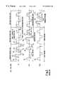
- FIG. 3schematically illustrates a frame structure of a first preferred embodiment of a drive waveform for driving a panel in accordance with the present invention.
- a frame FM to drive a single picture on a flat display panelsuch as a PDP or an electroluminescent panel, is formed of a plurality of, for example, eight subframes SF 1 to SF 8 .
- Each subframeis formed of an address period CYa and one of display periods CYi 1 . . . CYi 8 subsequent to each address period CYa 1 . . . CYa 8 .
- the cells to be litare addressed by being written selectively from all the remaining cells of the panel.
- the display periods CYi 1 to CYi 8have respective, different time lengths, essentially having a ratio 1:2:4:8:16:32:64:128, so that respective, different numbers of sustain pulses of a common frequency are included, approximately in proportion to this ratio, in the display periods of the respective subframes.
- Visual brightnessi.e., the gradation of the brightness of a lit cell is determined by the number of the sustain pulses accumulated for the single (i.e., individual) frame period.
- the gradation of 256 grades, defined by 8 bitscan be determined for each cell by selectively operating one or a plurality of the eight subframes.
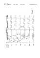
- FIG. 4shows voltage waveforms applied across the cells of an opposed-discharge type PDP of the invention, as hereinabove described, where a discharge takes place between matrix electrodes coated with insulating layers formed respectively on two glass panels facing each other.
- a layout of the matrix electrodesis schematically shown in FIG. 6; for the present explanation of the invention, the X-electrodes X f , X f ⁇ 1 , X f ⁇ 2 . . . are data electrodes and the Y-electrodes Y j , Y j+1 , Y j+2 . . . are scan electrodes.
- Cells Care formed at crossing points, or intersections, of the X-electrodes and the Y-electrodes.
- FIG. 5Voltage waveforms respectively applied to each of the X-electrodes and the Y-electrodes and producing the cell voltages of FIG. 4 are shown in FIG. 5.
- a sustain pulse Ps 1is applied to all the Y-electrodes in the same polarity as the subsequent write pulse; in other words, each sequence of sustain pulses ends at a sustain pulse having the polarity of the write pulse.
- Su'stain pulsesare typically 95 volt high and 5 ⁇ s long.
- a write pulse Pwis applied to all the cells by applying a pulse Pw concurrently to all the Y-electrodes while the X-electrodes are kept at 0 volt; the write pulse Pw is typically 150 volt high and 5 ⁇ s long, adequate for both igniting a discharge as well as forming a wall charge (see FIG. 10 ), as a memory medium, in all the cells.
- a second sustain pulse Ps 2having a polarity opposite to that of the write pulse Pw is applied to all the cells by applying the sustain pulse voltage Psx to all the X-electrodes while the Y electrodes are kept at 0 volt, in order to invert the wall charge by which the subsequent erase pulse Pf can be effective.
- an erase pulse Pfof typically 95 volt and 0.7 to 1 ⁇ s duration, is applied sequentially to each of the Y-electrodes; in other words, the Y-electrodes are scanned individually and in succession.
- a cancel pulse Pchaving substantially the same level and the same width as the erase pulse Pf is selectively applied to an X-electrode connected to a cell to be lit, in order to cancel the function of the erase pulse Pf.
- the pulse widthis not sufficiently long so as to accumulate an adequate wall charge to provide the memory function. That is, the wall charge is erased so that the cell, so addressed, is not lit later. Thereby the writing operation, which has addressed the cells to be lit by cancelling the function of the erase pulse, is completed throughout the panel.
- the address periodis approximately 621 ⁇ s long for a 400-line picture.
- a sustain pulse Ps 1is not applied, in other words, if the display period ends at the sustain pulse having the polarity opposite to the write pulse, the change in the cell voltage upon the following application of the write pulse is equal to the sum of the voltage levels of the sustain pulse and the write pulse. This large change in the cell voltage may cause a deterioration of the insulation layers of the cell.
- the sustain pulse Ps 1is preferably introduced into the address period, but is not absolutely necessary. In each address cycle, all the cells are lit three (3) times, namely, by the sustain pulse Psy, the write pulse Pw and the erase pulse Pf; however, these three (3) lightings are negligible compared with the far larger number of cell lightings produced in the display cycles.
- a first display period CYi 1is approximately 46 ⁇ s long.
- the sustain pulsesare typically 5 ⁇ s wide and typically have a 2 ⁇ s interval therebetween; therefore, three pairs of the sustain pulses of frequency 71.4 kHz are included in the first display period CYi 1 .
- the sustain pulsesare applied to all the cells by applying the sustain pulse voltage Psy, in a current phase, to all the Y-electrodes and, in the next phase, by applying the sustain pulse voltage Psx to all the X-electrodes.
- the cells which were addressed, i.e., having the wall charge, in the first address period CYa 1are lit by the sustain pulses in the subsequent display period CYi 1 of subframe SF 1 .
- the first subframe SF 1is now completed.
- the cells to be lit during the second display period CYi 2are addressed in the same way as in the first address period.
- the second display period CYi 2subsequent to the second address period CYa 2 , is approximately 91 ⁇ s long, so as to contain 6 pairs of sustain pulses.
- the frequencymay be varied for each subframe, such as 0.75, 1.5, 3, 6, 12, 24, 48 and 96 kHz, where the numbers of the sustain pulse pairs are 1, 2, 4, 8, 17, n35, 70 and 140, respectively.
- sustain pulsesmay be of a constant frequency, such as 96 kHz, where unnecessary pulses are killed (i.e., deleted, or blanked) so as to leave a necessary, i.e., appropriate, number of sustain pulses in each display period.
- a second preferred embodiment of the present invention, applied to a surface discharge type PDP,is hereinafter described.
- the surface discharge type PDPmay be of the widely known type disclosed in Japanese Unexamined Patent Publication Tokukai Sho 57-78751 and 61-39341, or schematically illustrated in FIG. 8.
- a plurality of X-electrodes Xparallel to and positioned close to respective ones of a plurality of Y-electrodes Y j , Y j ⁇ 1 , Y j ⁇ 2 . . . , and plural address electrodes An, An+1, An+2, . . . orthogonal to the X and Y electrodes, are arranged on a surface of a panel.
- Electrodes crossing each otherare insulated with an insulating layer.
- An address cell Cais formed at each of the crossed points of the Y-electrodes Y j , Y j+1 , Y j+2 and the address electrodes An, An+1, An+2, . . . .
- Display cells Cdare formed between the adjacent, associated Y-electrode and X-electrode, close to the corresponding address cells Ca, respectively.
- Voltage waveforms applied to the X-electrodes X, the Y-electrodes Y j , Y j+1 , Y j+2 , . . . and the address electrode Anare shown in FIG. 7 .
- An address period CYais performed concurrently with respect to all the Y-electrodes.
- a write pulse Pwtypically 5 ⁇ s long and 90 volt high
- a first sustain pulse Psy 1that is opposite in polarity to the write pulse Pw and typically 5 ⁇ s long and 150 volt high
- a second sustain pulse Psxtypically 5 ⁇ s long and 150 volt high and of an opposite polarity to the write pulse Pw, is applied to all the X-electrodes, so that a wall charge is generated in each display cell Cd and in a part of the associated address cell Ca.
- an erase pulse Pftypically 150 volt high and 3 ⁇ long
- an address pulse Patypically 90 volt high and 3 ⁇ long
- the wall chargeis maintained.
- sustain pulsestypically 150 volt high and 5 ⁇ s long, are applied to all the cells by applying sustain pulses Psy to all the Y-electrodes and sustain pulses Psx alternately to all the X-electrodes.
- the cells having been addressed to have the wall chargeare lit by the sustain pulses.
- the same operationsare repeated as those of the first subframe, except that the respective time lengths of the display periods are different in each subframe, as the same way as that of the first preferred embodiment.
- the time length allocated to each subframeis identical to that of the first preferred embodiment. Accordingly, the same advantageous effects can be accomplished in the second embodiment, as well.
- time length allocationis done in such a manner that the first subframe has the shortest display period and the last subframe has the longest display period, it is apparent that the order of the time length allocation is arbitrarily chosen.
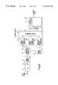
- FIG. 9shows a block diagram of a driving circuit of the present invention for providing gradation of the visual brightness of a flat matrix panel.
- An analog input signal S 1of picture data to be displayed, is converted by an A/D converter 11 to a digital signal D 2 .
- a frame memory 12stores the digital signal D 2 of a single frame FM output from A/D converter 11 .
- a subframe generator 13divides a single frame of picture data D 2 stored in the frame memory 12 into plural subframes SF 1 , SF 2 . . . according to the required gradation level, so as to output respective subframe data D 3 .
- a scanning circuit 14scans a Y-electrode driver 31 and an X-electrode driver 32 of the display panel 4 .
- the scanning circuit 14comprises a cancel pulse generator 21 to generate the cancel pulses Pc of the first preferred embodiment as well as the address pulses Pa of the second preferred embodiment; a write pulse generator 22 to generate the write pulses Pw; a sustain pulse generator 23 to generate the sustain pulses Ps; and a composer (i.e., combiner) circuit 24 to compose, or combine, these signals.
- a timing controller 15outputs several kinds of timing signals for timing functions, such as process timing of subframe generator 13 , output timing of the cancel pulse generator, and termination of timing of the display period, in each subframe.
- subframe generator (processor) 13sequentially outputs n kinds of binary data D 3 , i.e., pixel position data identifying the position of each pixel to be selected, or turned ON, in each subframe, of a picture to be exclusively formed of the respective gradation bits for each pixel, in the order from the least significant bit to the most significant bit and thus from the brightness data of the lowest level up to the brightness data of the highest level bit.
- the cancel pulse generator 21outputs cancel pulses Pc, at the moment when a line is selected, to X-electrodes connected to the cells to be addressed, and thus to be lighted, on this selected Y-electrode.
- Timing controller 15outputs a timing control signal so that the time length of each display period of subframes becomes a predetermined length in accordance with picture data D 3 for the pixel position data output from subframe processor (generator) 13 .
- Composer (combiner) circuit 24outputs the scan voltages shown in FIG. 5 by combining the respective pulse signals output from the pulse generators 21 , 22 and 23 so that the address period CYa and the display hit) period CYi can be executed in each subframe SF.
- the erase/cancel pulsesmay be as short, or brief, as 1 ⁇ s and may require only 600 ⁇ s for addressing the cells to be lit on the 400 lines after the concurrent application of the write pulse to all the cells.
- the amount of time required for the addressing operationis drastically decreased, compared with the FIG. 1 prior art method wherein the duration of the write pulses Pw, i.e., as long as 5 ⁇ s, occupy about 2.2 ms for individually addressing the 400 lines.
- the time for the display periodsmay be as large as 11.7 ms, which is enough to provide a 256-grade gradation.
- the driving frequencycan be lowered in accomplishing the same gradation level. The lower driving frequency lowers the power consumption in the driving circuit, as well as allows a longer pulse width, which provides more margin in the operation reliability.
- the method of the present inventionsolves the prior art problem in that the driving circuit configuration is complicated, because the write period CYw of a line must be executed concurrently to the sustain period CYm of the other lines; accordingly, the pulses must be of very high frequency.
- the number of sustain pulses in each subframecan be easily chosen because the display period CY 1 is completely independent of the address period CYa, since the cycle of the sustain pulses does not need to synchronize with the cycle of the address cycle.
- the gradationcan be easily controlled, the ratio of the respective time duration of the display periods in the subframes can be arbitrarily and easily chosen so that the gradation can meet the gamma characteristics of human eyes and, accordingly, the present invention is advantageous in affording freedom in designing the circuit, the production cost and the product reliability, as well.
- the addressing operationis carried out by canceling the once-written cells, it is apparent that the addressing method may be of other conventional methods wherein the writing operation is carried out only on the cells to be lit, without “writing-all” and “erasing-some-of-them.” Even in this case, the same advantageous effect can be achieved as in the above preferred embodiments.
- an AC-type PDPis referred to in which the memory medium is formed of a wall charge
- the present inventionmay be embodied in other flat panels where the memory medium is formed of a space charge (see FIG. 11 ), such as a DC-type PDP, an EL (electroluminescent) display device, or a liquid crystal device.
Landscapes
- Engineering & Computer Science (AREA)
- Physics & Mathematics (AREA)
- Plasma & Fusion (AREA)
- Computer Hardware Design (AREA)
- General Physics & Mathematics (AREA)
- Theoretical Computer Science (AREA)
- Power Engineering (AREA)
- Control Of Indicators Other Than Cathode Ray Tubes (AREA)
- Control Of Gas Discharge Display Tubes (AREA)
Abstract
Description
| display period time length: | number of sustain pulse pairs: |
| 1st SF | approx. | 45 | μs | approx. | 3 |
| 2nd SF | 91 | 6 | |||
| 3rd SF | 182 | 13 | |||
| 4th SF | 365 | 26 | |||
| 5th SF | 730 | 52 | |||
| 6th SF | 1,461 | 104 | |||
| 7th SF | 2,924 | 209 | |||
| 8th SF | 5,845 | 418 | |||
| total | 831 | ||||
Claims (12)
Priority Applications (1)
| Application Number | Priority Date | Filing Date | Title |
|---|---|---|---|
| US09/451,351US6630916B1 (en) | 1990-11-28 | 1999-12-03 | Method and a circuit for gradationally driving a flat display device |
Applications Claiming Priority (22)
| Application Number | Priority Date | Filing Date | Title |
|---|---|---|---|
| JP33158990AJP3259253B2 (en) | 1990-11-28 | 1990-11-28 | Gray scale driving method and gray scale driving apparatus for flat display device |
| JP2-331589 | 1990-11-28 | ||
| US79925591A | 1991-11-27 | 1991-11-27 | |
| JP4012976AJP2731480B2 (en) | 1992-01-28 | 1992-01-28 | Surface discharge type plasma display panel |
| JP4-012976 | 1992-01-28 | ||
| JP4-96203 | 1992-04-16 | ||
| JP9620392AJP3054489B2 (en) | 1992-04-16 | 1992-04-16 | Method for manufacturing plasma display panel |
| JP4106955AJP3007751B2 (en) | 1992-04-24 | 1992-04-24 | Method for manufacturing plasma display panel |
| JP4-106953 | 1992-04-24 | ||
| JP4-106955 | 1992-04-24 | ||
| JP10695392AJP3270511B2 (en) | 1992-04-24 | 1992-04-24 | Surface discharge type plasma display panel |
| JP11092192AJP3272396B2 (en) | 1992-04-30 | 1992-04-30 | Plasma display device |
| JP4-110921 | 1992-04-30 | ||
| US1016993A | 1993-01-28 | 1993-01-28 | |
| US18195994A | 1994-01-18 | 1994-01-18 | |
| US08/405,920US5541618A (en) | 1990-11-28 | 1995-03-16 | Method and a circuit for gradationally driving a flat display device |
| US08/458,288US5674553A (en) | 1992-01-28 | 1995-06-02 | Full color surface discharge type plasma display device |
| US08/469,815US5661500A (en) | 1992-01-28 | 1995-06-06 | Full color surface discharge type plasma display device |
| US08/674,161US5724054A (en) | 1990-11-28 | 1996-07-01 | Method and a circuit for gradationally driving a flat display device |
| US08/800,759US6195070B1 (en) | 1992-01-28 | 1997-02-13 | Full color surface discharge type plasma display device |
| US08/888,442US6097357A (en) | 1990-11-28 | 1997-07-03 | Full color surface discharge type plasma display device |
| US09/451,351US6630916B1 (en) | 1990-11-28 | 1999-12-03 | Method and a circuit for gradationally driving a flat display device |
Related Parent Applications (2)
| Application Number | Title | Priority Date | Filing Date |
|---|---|---|---|
| US08/674,161Continuation-In-PartUS5724054A (en) | 1990-11-28 | 1996-07-01 | Method and a circuit for gradationally driving a flat display device |
| US08/888,442ContinuationUS6097357A (en) | 1990-11-28 | 1997-07-03 | Full color surface discharge type plasma display device |
Related Child Applications (1)
| Application Number | Title | Priority Date | Filing Date |
|---|---|---|---|
| US08/458,288DivisionUS5674553A (en) | 1990-11-28 | 1995-06-02 | Full color surface discharge type plasma display device |
Publications (1)
| Publication Number | Publication Date |
|---|---|
| US6630916B1true US6630916B1 (en) | 2003-10-07 |
Family
ID=27584129
Family Applications (2)
| Application Number | Title | Priority Date | Filing Date |
|---|---|---|---|
| US08/888,442Expired - Fee RelatedUS6097357A (en) | 1990-11-28 | 1997-07-03 | Full color surface discharge type plasma display device |
| US09/451,351Expired - Fee RelatedUS6630916B1 (en) | 1990-11-28 | 1999-12-03 | Method and a circuit for gradationally driving a flat display device |
Family Applications Before (1)
| Application Number | Title | Priority Date | Filing Date |
|---|---|---|---|
| US08/888,442Expired - Fee RelatedUS6097357A (en) | 1990-11-28 | 1997-07-03 | Full color surface discharge type plasma display device |
Country Status (1)
| Country | Link |
|---|---|
| US (2) | US6097357A (en) |
Cited By (297)
| Publication number | Priority date | Publication date | Assignee | Title |
|---|---|---|---|---|
| US20020018029A1 (en)* | 2000-08-08 | 2002-02-14 | Jun Koyama | Electro-optical device and driving method of the same |
| US20020024485A1 (en)* | 2000-08-08 | 2002-02-28 | Jun Koyama | Liquid crystal display device and driving method thereof |
| US20020024054A1 (en)* | 2000-08-18 | 2002-02-28 | Jun Koyama | Electronic device and method of driving the same |
| US20020041266A1 (en)* | 2000-10-05 | 2002-04-11 | Jun Koyama | Liquid crystal display device |
| US20020105270A1 (en)* | 2001-01-16 | 2002-08-08 | Yoshitaka Terao | Plasma display and manufacturing method thereof |
| US20020172613A1 (en)* | 2000-06-30 | 2002-11-21 | Kunio Fukuda | Fe-cr-al based alloy foil and method for producing the same |
| US20030218432A1 (en)* | 2002-05-24 | 2003-11-27 | Yoo-Jin Song | Automatic power control (APC) method and device of plasma display panel (PDP) and PDP device having the APC device |
| US20030234755A1 (en)* | 2002-06-06 | 2003-12-25 | Jun Koyama | Light-emitting device and method of driving the same |
| US20040008162A1 (en)* | 2002-07-12 | 2004-01-15 | Jin-Sung Kim | Method of driving 3-electrode plasma display apparatus to minimize addressing power |
| US20040061669A1 (en)* | 2002-07-23 | 2004-04-01 | Kang Kyoung-Ho | Plasma display panel and method for driving the same |
| US20040075625A1 (en)* | 2002-07-08 | 2004-04-22 | Joon-Koo Kim | Apparatus and method for driving plasma display panel to enhance display of gray scale and color |
| US20040090170A1 (en)* | 2002-11-06 | 2004-05-13 | Jun-Kyu Cha | Filter for plasma display panel and method of manufacturing the same |
| US20040091672A1 (en)* | 2002-11-05 | 2004-05-13 | Jung-Keun Ahn | Plasma display panel |
| US20040100425A1 (en)* | 2002-11-26 | 2004-05-27 | Kang Kyoung-Ho | Method and apparatus for driving panel by performing mixed address period and sustain period |
| US20040113553A1 (en)* | 2002-12-17 | 2004-06-17 | Cha-Keun Yoon | Plasma display panel |
| US20040130265A1 (en)* | 2002-08-02 | 2004-07-08 | Yoshitaka Terao | Plasma display panel and manufacturing method thereof |
| US20040150340A1 (en)* | 2002-12-31 | 2004-08-05 | Seung-Hyun Son | Plasma display panel including sustain electrodes having double gap and method of manufacturing the panel |
| US20040150588A1 (en)* | 2003-01-15 | 2004-08-05 | Samsung Sdi Co., Ltd. | Plasma display panel and gray display method thereof |
| US20040164677A1 (en)* | 2003-02-21 | 2004-08-26 | Tae-Ho Lee | Plasma display panel and method of manufacture thereof |
| US20040212554A1 (en)* | 2003-04-28 | 2004-10-28 | Ki-Jung Kim | Plasma display device that efficiently and effectively draws heat out from a functioning plasma display panel |
| US20040217922A1 (en)* | 2003-04-29 | 2004-11-04 | Takahisa Mizuta | Plasma display panel and driving method thereof |
| US20040222955A1 (en)* | 2001-02-09 | 2004-11-11 | Semiconductor Energy Laboratory Co., Ltd. A Japan Corporation | Liquid crystal display device and method of driving the same |
| US20040232843A1 (en)* | 2003-05-21 | 2004-11-25 | Kim Gi-Young | Plasma display panel and method of forming address electrodes thereof |
| US20040257307A1 (en)* | 2003-06-23 | 2004-12-23 | Sung-Won Bae | Plasma display device |
| US20050007314A1 (en)* | 2001-01-18 | 2005-01-13 | Lg Electronics Inc. | Method and apparatus for expressing gray level with decimal value in plasma display panel |
| US20050017962A1 (en)* | 2003-07-22 | 2005-01-27 | Pioneer Corporation | Driving apparatus of display panel |
| US20050017638A1 (en)* | 2003-07-22 | 2005-01-27 | Woo-Tae Kim | Plasma display device |
| US20050023977A1 (en)* | 2003-07-29 | 2005-02-03 | Jeong-Chull Ahn | Plasma display panel |
| US20050035931A1 (en)* | 2003-08-12 | 2005-02-17 | Hun-Suk Yoo | Plasma display panel driving method and plasma display device |
| US20050035713A1 (en)* | 2003-08-13 | 2005-02-17 | Sung-Hune Yoo | Plasma display panel |
| US20050040767A1 (en)* | 2003-08-18 | 2005-02-24 | Sung-Hune Yoo | Plasma display panel using color filters to improve contrast |
| US20050046618A1 (en)* | 2003-09-01 | 2005-03-03 | Sok-San Kim | Plasma display module with improved heat dissipation characteristics |
| US20050046353A1 (en)* | 2003-09-02 | 2005-03-03 | Jae-Ik Kwon | Address electrode design in a plasma display panel |
| US20050052138A1 (en)* | 2003-09-08 | 2005-03-10 | Tae-Joung Kweon | Plasma display panel and method of manufacturing the same resulting in improved contrast and improved chromaticity |
| US20050052137A1 (en)* | 2003-09-04 | 2005-03-10 | Jae-Ik Kwon | Plasma display panel |
| US20050052359A1 (en)* | 2003-09-04 | 2005-03-10 | Jae-Ik Kwon | Plasma display panel |
| US20050052358A1 (en)* | 2003-09-09 | 2005-03-10 | In-Soo Cho | Heat dissipating sheet and plasma display device including the same |
| US20050057444A1 (en)* | 2003-09-01 | 2005-03-17 | Ji-Sung Ko | Plasma display panel |
| US20050062418A1 (en)* | 2003-09-04 | 2005-03-24 | Kang Tae-Kyoung | Plasma display panel |
| US20050067957A1 (en)* | 2002-09-27 | 2005-03-31 | Moon Cheol-Hee | Plasma display panel |
| US20050068265A1 (en)* | 2003-09-26 | 2005-03-31 | Mi-Young Joo | Method and apparatus to automatically control power of address data for plasma display panel, and plasma display panel including the apparatus |
| US20050073477A1 (en)* | 2003-10-01 | 2005-04-07 | Sung-Hune Yoo | Plasma display panel (PDP) |
| US20050073484A1 (en)* | 2003-10-01 | 2005-04-07 | Kim Se-Woong | Driving apparatus of plasma display panel and method for displaying pictures on plasma display panel |
| US20050078063A1 (en)* | 2003-10-09 | 2005-04-14 | Yong-Seok Chi | Plasma display panel and driving method thereof |
| US20050077823A1 (en)* | 2003-10-09 | 2005-04-14 | Song Young-Hwa | Plasma display panel |
| US20050077835A1 (en)* | 2003-10-08 | 2005-04-14 | Ki-Jung Kim | Thermal conductive medium for display device, method of fabricating the same, and plasma display panel assembly using the same |
| US20050077836A1 (en)* | 2003-10-14 | 2005-04-14 | Kwang-Ho Jin | Discharge display apparatus minimizing addressing power and method of driving the same |
| US20050082979A1 (en)* | 2003-10-16 | 2005-04-21 | Eun-Young Jung | Plasma display panel |
| US20050083258A1 (en)* | 2003-10-21 | 2005-04-21 | Im-Su Choi | Method of expressing gray level of high load image and plasma display panel driving apparatus using the method |
| US20050083265A1 (en)* | 2003-10-16 | 2005-04-21 | Mi-Young Joo | Plasma display panel device, white linearity control device and control method thereof |
| US20050083254A1 (en)* | 2003-10-21 | 2005-04-21 | Jang Tae-Woong | Plasma display panel |
| US20050088097A1 (en)* | 2003-10-24 | 2005-04-28 | Sung-Won Bae | Plasma display device |
| US20050088092A1 (en)* | 2003-10-17 | 2005-04-28 | Myoung-Kon Kim | Plasma display apparatus |
| US20050088096A1 (en)* | 2003-10-28 | 2005-04-28 | Sung-Hune Yoo | Plasma display panel (PDP) with multiple dielectric layers |
| US20050088071A1 (en)* | 2003-10-23 | 2005-04-28 | Joong-Ha Ahn | Plasma display apparatus having heat dissipating structure for driver integrated circuit |
| US20050093448A1 (en)* | 2003-10-31 | 2005-05-05 | Moon Cheol-Hee | Plasma display panel provided with an improved electrode |
| US20050093446A1 (en)* | 2003-10-09 | 2005-05-05 | Chong-Gi Hong | Plasma display panel and method of manufacturing back panel thereof |
| US20050093447A1 (en)* | 2003-10-31 | 2005-05-05 | Byung-Soo Jeon | Plasma display panel |
| US20050093451A1 (en)* | 2003-10-30 | 2005-05-05 | Tae-Joung Kweon | Method of forming a dielectric film and plasma display panel using the dielectric film |
| US20050093444A1 (en)* | 2003-10-29 | 2005-05-05 | Seok-Gyun Woo | Plasma display panel |
| US20050099106A1 (en)* | 2003-11-08 | 2005-05-12 | Ki-Jung Kim | Plasma display apparatus |
| US20050099126A1 (en)* | 2003-11-11 | 2005-05-12 | Young-Mo Kim | Plasma display panel with discharge cells having curved concave-shaped walls |
| US20050104520A1 (en)* | 2003-11-17 | 2005-05-19 | Chong-Gi Hong | Plasma display panel and method of manufacturing the plasma display panel |
| US20050104518A1 (en)* | 2003-10-21 | 2005-05-19 | Chong-Gi Hong | Plasma display panel having high brightness and high contrast |
| US20050104519A1 (en)* | 2003-11-13 | 2005-05-19 | Byung-Soo Jeon | Plasma display panel |
| US20050111175A1 (en)* | 2003-10-16 | 2005-05-26 | Dae-Gyu Kim | Plasma display module |
| US20050110407A1 (en)* | 2003-11-26 | 2005-05-26 | Chun-Soo Kim | Plasma display device |
| US20050110408A1 (en)* | 2003-11-26 | 2005-05-26 | Jang Sang-Hun | Plasma display panel |
| US20050110709A1 (en)* | 2003-11-24 | 2005-05-26 | Lee Joo-Yul | Driving a plasma display panel (PDP) |
| US20050110707A1 (en)* | 2003-11-22 | 2005-05-26 | Im-Su Choi | Method and apparatus for driving discharge display panel to improve linearity of gray-scale |
| US20050116642A1 (en)* | 2003-11-29 | 2005-06-02 | Moon Cheol-Hee | Plasma display panel and method of manufacturing the same |
| US20050116640A1 (en)* | 2003-10-16 | 2005-06-02 | Sung-Hune Yoo | Plasma display panel |
| US20050117304A1 (en)* | 2003-11-28 | 2005-06-02 | Ki-Jung Kim | Device having improved heat dissipation |
| US20050116646A1 (en)* | 2003-11-29 | 2005-06-02 | Hun-Suk Yoo | Plasma display panel |
| US20050116643A1 (en)* | 2003-11-27 | 2005-06-02 | Yi-Hyun Chang | Plasma display panel (PDP) |
| US20050116648A1 (en)* | 2003-11-29 | 2005-06-02 | Byung-Kwan Song | Plasma display panel and method for manufacturing the same |
| US20050116641A1 (en)* | 2003-11-29 | 2005-06-02 | Seung-Uk Kwon | Green phosphor for plasma display panel (PDP) |
| US20050140581A1 (en)* | 2003-11-29 | 2005-06-30 | Kyoung-Doo Kang | Method of driving plasma display panel (PDP) |
| US20050140579A1 (en)* | 2003-09-08 | 2005-06-30 | Sung-Hune Yoo | Structure for a plasma display panel that reduces capacitance between electrodes |
| US20050140580A1 (en)* | 2003-11-24 | 2005-06-30 | Joon-Suk Baik | Method of driving plasma display panel |
| US20050148151A1 (en)* | 2003-11-29 | 2005-07-07 | Jong-Sang Lee | Plasma display panel and manufacturing method thereof |
| US20050156525A1 (en)* | 2004-01-17 | 2005-07-21 | Kyu-Nam Joo | Filter assembly, method of manufacturing the same, and plasma display panel using the same |
| US20050162062A1 (en)* | 2004-01-26 | 2005-07-28 | Sung-Yong Lee | Green phosphor for plasma display panel and plasma display panel comprising the same |
| US20050168405A1 (en)* | 2004-01-29 | 2005-08-04 | Jun-Young Lee | Method of driving plasma display panel and plasma display device |
| US20050174301A1 (en)* | 2004-02-10 | 2005-08-11 | Sok-San Kim | Plasma display module |
| US20050179384A1 (en)* | 2004-02-18 | 2005-08-18 | Jae-Ik Kwon | Plasma display panel (PDP) |
| US20050184663A1 (en)* | 2004-02-25 | 2005-08-25 | Moon Cheol-Hee | Plasma display apparatus |
| US20050184664A1 (en)* | 2004-02-21 | 2005-08-25 | Kang Tae-Kyoung | Plasma display device |
| US20050190201A1 (en)* | 2002-07-23 | 2005-09-01 | Baer David A. | System and method for providing graphics using graphical engine |
| US20050190120A1 (en)* | 2004-02-26 | 2005-09-01 | Hun-Suk Yoo | Display panel driving method |
| US20050194900A1 (en)* | 2004-03-04 | 2005-09-08 | Hyouk Kim | Plasma display apparatus |
| US20050212425A1 (en)* | 2004-03-26 | 2005-09-29 | Hun-Suk Yoo | Plasma display panel |
| US20050212423A1 (en)* | 2004-03-24 | 2005-09-29 | Jae-Ik Kwon | Plasma display panel |
| US20050213010A1 (en)* | 2004-03-26 | 2005-09-29 | Jae-Ik Kwon | Plasma display panel |
| US20050212424A1 (en)* | 2004-03-25 | 2005-09-29 | Jae-Ik Kwon | Plasma display panel having electromagnetic wave shielding layer |
| US20050225242A1 (en)* | 2004-04-13 | 2005-10-13 | Seok-Gyun Woo | Plasma display panel (PDP) |
| US20050225244A1 (en)* | 2004-04-09 | 2005-10-13 | Jeong-Chul Ahn | Plasma display panel |
| US20050225504A1 (en)* | 2004-04-12 | 2005-10-13 | Sang-Chul Kim | Plasma display panel (PDP) and method of driving PDP |
| US20050225241A1 (en)* | 2004-04-09 | 2005-10-13 | Seok-Gyun Woo | Plasma display panel |
| US20050225245A1 (en)* | 2004-04-09 | 2005-10-13 | Seung-Beom Seo | Plasma display panel |
| US20050231113A1 (en)* | 2004-04-19 | 2005-10-20 | Kyoung-Doo Kang | Plasma display panel |
| US20050231116A1 (en)* | 2004-04-20 | 2005-10-20 | Hun-Suk Yoo | High efficiency plasma display panel (PDP) |
| US20050231111A1 (en)* | 2004-04-20 | 2005-10-20 | Seok-Gyun Woo | Plasma display panel |
| US20050231115A1 (en)* | 2004-04-16 | 2005-10-20 | Jae-Ik Kwon | Plasma display panel |
| US20050231109A1 (en)* | 2004-04-20 | 2005-10-20 | Hun-Suk Yoo | Plasma display panel (PDP) having electromagnetic wave shielding electrodes |
| US20050231112A1 (en)* | 2004-04-19 | 2005-10-20 | Seok-Gyun Woo | Plasma display panel and method of manufacturing the same |
| US20050231110A1 (en)* | 2004-04-19 | 2005-10-20 | Seok-Gyun Woo | Plasma Display Panel (PDP) |
| US20050236986A1 (en)* | 2004-04-27 | 2005-10-27 | Jae-Ik Kwon | Plasma display panel (PDP) |
| US20050236990A1 (en)* | 2004-04-27 | 2005-10-27 | Woo-Tae Kim | Plasma display panel |
| US20050236988A1 (en)* | 2004-04-12 | 2005-10-27 | Jae-Ik Kwon | Plasma display panel |
| US20050242722A1 (en)* | 2004-05-01 | 2005-11-03 | Hun-Suk Yoo | Plasma display panel |
| US20050242724A1 (en)* | 2004-04-28 | 2005-11-03 | Woo-Tae Kim | Plasma display panel |
| US20050243106A1 (en)* | 2004-04-29 | 2005-11-03 | Sung-Won Bae | Plasma display apparatus |
| US20050242729A1 (en)* | 2004-04-28 | 2005-11-03 | Tae-Joung Kweon | Plasma display panel |
| US20050242683A1 (en)* | 2004-04-30 | 2005-11-03 | Johnson Electric S.A. | Brush assembly |
| US20050242723A1 (en)* | 2004-05-01 | 2005-11-03 | Hun-Suk Yoo | Plasma display panel |
| US20050243026A1 (en)* | 2004-04-29 | 2005-11-03 | Tae-Seong Kim | Plasma display panel driving method and plasma display |
| US20050248273A1 (en)* | 2004-05-07 | 2005-11-10 | Tae-Joung Kweon | Plasma display panel |
| US20050258747A1 (en)* | 2004-05-21 | 2005-11-24 | Su-Bin Song | Plasma display panel (PDP) |
| US20050259048A1 (en)* | 2004-05-24 | 2005-11-24 | Min Hur | Plasma display panel and a drive method therefor |
| US20050258748A1 (en)* | 2004-05-18 | 2005-11-24 | Kyoung-Doo Kang | Plasma display panel (PDP) |
| US20050259045A1 (en)* | 2004-05-21 | 2005-11-24 | Seung-Beom Seo | Plasma display panel (PDP) |
| US20050258751A1 (en)* | 2004-05-24 | 2005-11-24 | Kang Tae-Kyoung | Plasma display panel |
| US20050264203A1 (en)* | 2004-05-31 | 2005-12-01 | Min Hur | Plasma display panel |
| US20050264486A1 (en)* | 2004-05-25 | 2005-12-01 | Seung-Hun Chae | Plasma display panel and driving method thereof |
| US20050264201A1 (en)* | 2004-05-31 | 2005-12-01 | Kyoung-Doo Kang | Plasma display panel |
| US20050264204A1 (en)* | 2004-05-28 | 2005-12-01 | Tae-Ho Lee | Plasma Display Panel (PDP) |
| US20050264233A1 (en)* | 2004-05-25 | 2005-12-01 | Kyu-Hang Lee | Plasma display panel (PDP) |
| US20050264478A1 (en)* | 2004-05-25 | 2005-12-01 | Jae-Ik Kwon | Plasma Display Panel (PDP) |
| US20050264476A1 (en)* | 2004-05-25 | 2005-12-01 | Duck-Hyun Kim | Plasma display device and driving method of plasma display panel |
| US20050271979A1 (en)* | 2004-06-07 | 2005-12-08 | Beom-Wook Lee | Photosensitive paste composition, PDP electrode prepared therefrom, and PDP comprising the PDP electrode |
| US20050280368A1 (en)* | 2004-06-18 | 2005-12-22 | Jung-Keun Ahn | Plasma display panel (PDP) |
| US20050285529A1 (en)* | 2004-06-23 | 2005-12-29 | Eui-Jeong Hwang | Plasma display panel |
| US20060001378A1 (en)* | 2004-06-30 | 2006-01-05 | Jeong-Doo Yi | Plasma display panel (PDP) |
| US20060001377A1 (en)* | 2004-06-30 | 2006-01-05 | Min Hur | Plasma display panel |
| US20060001375A1 (en)* | 2004-06-30 | 2006-01-05 | Min Hur | Plasma display panel (PDP) |
| US20060006802A1 (en)* | 2004-07-07 | 2006-01-12 | Kang Tae-Kyoung | Plasma display panel |
| US20060028404A1 (en)* | 2004-08-05 | 2006-02-09 | Kang Tae-Kyoung | Method and apparatus of driving plasma display panel |
| US20060028887A1 (en)* | 2004-08-03 | 2006-02-09 | Myoung-Kwan Kim | Plasma display panel (PDP) and driving method thereof |
| US20060033448A1 (en)* | 2004-06-30 | 2006-02-16 | Min Hur | Plasma display panel (PDP) |
| US20060033437A1 (en)* | 2004-08-13 | 2006-02-16 | Ki-Jong Eom | Plasma display panel |
| US20060038749A1 (en)* | 2004-08-18 | 2006-02-23 | Jun-Young Lee | Plasma display device and driving method thereof |
| US20060043894A1 (en)* | 2004-08-30 | 2006-03-02 | Yong-Jun Kim | Plasma display panel |
| US20060044231A1 (en)* | 2004-08-27 | 2006-03-02 | Tohoku Pioneer Corporation | Drive device and drive method of self light emitting display panel and electronic equipment equipped with the drive device |
| US20060076890A1 (en)* | 2004-10-12 | 2006-04-13 | Chong-Gi Hong | Plasma display panel (PDP) |
| US20060077619A1 (en)* | 2004-10-11 | 2006-04-13 | Ki-Jung Kim | Plasma display device |
| US20060076889A1 (en)* | 2004-10-13 | 2006-04-13 | Seung-Beom Seo | Plasma display panel (PDP) |
| US20060082274A1 (en)* | 2004-10-19 | 2006-04-20 | Jung-Suk Song | Panel assembly, plasma display panel assembly employing the same, and method of manufacturing plasma display panel assembly |
| US20060082306A1 (en)* | 2004-10-19 | 2006-04-20 | Jung-Suk Song | Plasma display panel (PDP) and its method of manufacture |
| US20060087235A1 (en)* | 2004-10-25 | 2006-04-27 | Kyoung-Doo Kang | Plasma display panel |
| US20060087238A1 (en)* | 2004-10-25 | 2006-04-27 | Jae-Ik Kwon | Plasma display panel |
| US20060091804A1 (en)* | 2004-11-04 | 2006-05-04 | Rho Chang-Seok | Plasma display panel (PDP) |
| US20060091803A1 (en)* | 2004-11-04 | 2006-05-04 | Seung-Uk Kwon | Plasma display panel (PDP) |
| US20060094323A1 (en)* | 2004-11-04 | 2006-05-04 | Chong-Gi Hong | Apparatus to form dielectric layer and method of manufacturing plasma display panel (PDP) with the apparatus |
| US20060091808A1 (en)* | 2004-10-28 | 2006-05-04 | Jang Sang-Hun | Plasma display panel |
| US20060091805A1 (en)* | 2004-10-28 | 2006-05-04 | Min Hur | Plasma display panel |
| US20060091802A1 (en)* | 2004-11-04 | 2006-05-04 | Chong-Gi Hong | Plasma display panel |
| US20060097638A1 (en)* | 2004-11-08 | 2006-05-11 | Seung-Hyun Son | Plasma display panel |
| US20060108926A1 (en)* | 2004-11-19 | 2006-05-25 | Min Hur | Plasma display panel |
| US20060115767A1 (en)* | 2004-11-30 | 2006-06-01 | Hyea-Weon Shin | Photo-sensitive composition, photo-sensitive paste composition for barrier ribs comprising the same, and method for preparing barrier ribs for plasma display panel |
| US20060113910A1 (en)* | 2004-11-29 | 2006-06-01 | Kyoung-Doo Kang | Plasma display panel |
| US20060113911A1 (en)* | 2004-11-29 | 2006-06-01 | Chong-Gi Hong | Plasma display panel |
| US20060119280A1 (en)* | 2004-12-08 | 2006-06-08 | Kim Se-Jong | Plasma display panel |
| US20060119241A1 (en)* | 2004-12-07 | 2006-06-08 | Jenn-Wei Mii | Automatic gas supplementing device for a discharge luminous tube |
| US20060119266A1 (en)* | 2004-12-04 | 2006-06-08 | Kyoung-Doo Kang | Plasma display panel (PDP) |
| US20060125395A1 (en)* | 2004-12-09 | 2006-06-15 | Kyoung-Doo Kang | Plasma display panel |
| US20060126314A1 (en)* | 2004-12-15 | 2006-06-15 | Kwang-Jin Jeong | Plasma display apparatus |
| US20060125399A1 (en)* | 2004-12-10 | 2006-06-15 | Jung-Hyuck Choi | Plasma display panel and method of manufacturing the same |
| US20060132946A1 (en)* | 2004-12-17 | 2006-06-22 | Sok-San Kim | Plasma display panel (PDP) assembly |
| US20060148294A1 (en)* | 2004-12-30 | 2006-07-06 | Sung-Won Bae | Plasma display panel (PDP) |
| US20060145609A1 (en)* | 2004-10-12 | 2006-07-06 | Chong-Gi Hong | Plasma display panel (PDP) |
| US20060145612A1 (en)* | 2005-01-05 | 2006-07-06 | Jae-Ik Kwon | Plasma display panel (PDP) |
| US20060146044A1 (en)* | 2004-12-30 | 2006-07-06 | Hidekazu Hatanaka | Flat discharge lamp and plasma display panel (PDP) |
| US20060154801A1 (en)* | 2005-01-11 | 2006-07-13 | Min-Suk Lee | Protecting layer, composite for forming the same, method of forming the protecting layer, plasma display panel comprising the protecting layer |
| US20060164011A1 (en)* | 2005-01-05 | 2006-07-27 | Beom-Wook Lee | Photosensitive paste composition, PDP electrode manufactured using the composition, and PDP including the PDP electrode |
| US20060166113A1 (en)* | 2005-01-05 | 2006-07-27 | Beom-Wook Lee | Photosensitive paste composition and plasma display panel manufactured using the same |
| US20060164012A1 (en)* | 2005-01-26 | 2006-07-27 | Tae-Joung Kweon | Plasma display panel (PDP) and flat panel display including the PDP |
| US20060170355A1 (en)* | 2005-02-03 | 2006-08-03 | Tae-Joung Kweon | Plasma display panel (PDP) |
| US20060170630A1 (en)* | 2005-02-01 | 2006-08-03 | Min Hur | Plasma display panel (PDP) and method of driving PDP |
| US20060170352A1 (en)* | 2005-02-01 | 2006-08-03 | Eun-Young Jung | Plasma display panel |
| US20060170350A1 (en)* | 2005-01-28 | 2006-08-03 | Ki-Jung Kim | Plasma display panel(PDP) |
| US20060175974A1 (en)* | 2005-02-04 | 2006-08-10 | Min Hur | Plasma display panel (PDP) |
| US20060192732A1 (en)* | 2002-05-27 | 2006-08-31 | Hitachi, Ltd. | Plasma display panel and imaging device using the same |
| US20060197450A1 (en)* | 2005-03-03 | 2006-09-07 | Jae-Ik Kwon | Dielectric layer structure and plasma display panel having the same |
| US20060202621A1 (en)* | 2005-03-09 | 2006-09-14 | Hun-Suk Yoo | Plasma display panel (PDP) |
| US20060208636A1 (en)* | 2005-03-17 | 2006-09-21 | Tae-Joung Kweon | Plasma display panel |
| US20060208638A1 (en)* | 2005-03-16 | 2006-09-21 | Hun-Suk Yoo | Plasma display panel |
| US20060208965A1 (en)* | 2005-03-15 | 2006-09-21 | Byoung-Min Chun | Plasma display panel (PDP) |
| US20060214598A1 (en)* | 2005-03-25 | 2006-09-28 | Kyoung-Doo Kang | Plasma display panel |
| US7122961B1 (en) | 2002-05-21 | 2006-10-17 | Imaging Systems Technology | Positive column tubular PDP |
| US20060238124A1 (en)* | 2005-04-22 | 2006-10-26 | Sung-Hune Yoo | Dielectric layer, plasma display panel comprising dielectric layer, and method of fabricating dielectric layer |
| US20060238125A1 (en)* | 2005-04-18 | 2006-10-26 | Min Hur | Plasma display panel |
| US20060238123A1 (en)* | 2005-04-26 | 2006-10-26 | Kyoung-Doo Kang | Plasma display panel |
| US20060255729A1 (en)* | 2005-05-16 | 2006-11-16 | Jae-Ik Kwon | Plasma display panel |
| US20060262241A1 (en)* | 2005-05-14 | 2006-11-23 | Kwang-Jin Jeong | Plasma display device |
| US20060267866A1 (en)* | 2005-05-13 | 2006-11-30 | Jai-Ik Kwon | Plasma display panel (PDP) |
| US20060275965A1 (en)* | 2005-05-24 | 2006-12-07 | Kwang-Jin Jeong | Plasma display device with improved heat dissipation efficiency |
| US20060279508A1 (en)* | 2005-06-14 | 2006-12-14 | Kyoung-Doo Kang | Apparatus to drive plasma display panel (PDP) |
| US20060279208A1 (en)* | 2005-06-13 | 2006-12-14 | Hwang Eui J | Plasma display panel |
| US20060291162A1 (en)* | 2005-06-28 | 2006-12-28 | Kim Yeung-Ki | Plasma display apparatus having improved structure and heat dissipation |
| US7157854B1 (en) | 2002-05-21 | 2007-01-02 | Imaging Systems Technology | Tubular PDP |
| US7161300B2 (en) | 2003-11-24 | 2007-01-09 | Samsung Sdi Co., Ltd. | Plasma display panel with two opposing fluorescent layers in VUV & UV discharge space |
| US20070008246A1 (en)* | 2005-07-08 | 2007-01-11 | Joon-Yeon Kim | Plasma display and a method of driving the plasma display |
| US20070007887A1 (en)* | 2005-07-07 | 2007-01-11 | Soh Hyun | Plasma display panel (PDP) |
| US20070024196A1 (en)* | 2005-08-01 | 2007-02-01 | Bong-Kyoung Park | Plasma display panel |
| US20070024202A1 (en)* | 2005-07-27 | 2007-02-01 | Il-Woon Lee | Power supply and plasma display including the power supply |
| US20070029942A1 (en)* | 2005-08-02 | 2007-02-08 | Seong-Joon Jeong | Plasma display and plasma display driver and method of driving plasma display |
| US20070035475A1 (en)* | 2005-08-10 | 2007-02-15 | Dong-Young Lee | Method of driving plasma display panel and plasma display apparatus driven using the method |
| US20070035247A1 (en)* | 2005-08-12 | 2007-02-15 | Seok-Gyun Woo | Plasma display panel (PDP) |
| US20070035244A1 (en)* | 2005-08-09 | 2007-02-15 | Dong-Young Lee | Plasma display panel (PDP) |
| US7180496B2 (en)* | 2000-08-18 | 2007-02-20 | Semiconductor Energy Laboratory Co., Ltd. | Liquid crystal display device and method of driving the same |
| US20070040507A1 (en)* | 2005-08-19 | 2007-02-22 | Kyoung-Doo Kang | Plasma display panel (PDP) |
| US20070040486A1 (en)* | 2005-08-17 | 2007-02-22 | Kim Yeung-Ki | Plasma display apparatus |
| US20070046202A1 (en)* | 2005-08-29 | 2007-03-01 | Kyoung-Doo Kang | Plasma display panel (PDP) |
| US20070046573A1 (en)* | 2005-08-27 | 2007-03-01 | Jong-Wook Kim | Driving method of plasma display panel (PDP) |
| US20070046208A1 (en)* | 2005-08-30 | 2007-03-01 | Kyoung-Doo Kang | Plasma display panel |
| US20070046207A1 (en)* | 2005-08-31 | 2007-03-01 | Hyun Kim | Plasma display panel |
| US20070046572A1 (en)* | 2005-08-26 | 2007-03-01 | Kyoung-Doo Kang | Plasma display panel (PDP) |
| US20070052359A1 (en)* | 2005-09-07 | 2007-03-08 | Sanghoon Yim | Micro discharge (MD) plasma display panel (PDP) |
| US20070063653A1 (en)* | 2005-09-07 | 2007-03-22 | Sang-Hoon Yim | Micro discharge (MD) plasma display panel (PDP) |
| US20070080633A1 (en)* | 2005-10-11 | 2007-04-12 | Kim Jeong-Nam | Plasma display panel |
| US20070082575A1 (en)* | 2005-10-07 | 2007-04-12 | Hyea-Weon Shin | Method for preparing plasma display panel |
| US20070085479A1 (en)* | 2005-10-13 | 2007-04-19 | Hwang Yong-Shik | Plasma display panel (PDP) and its method of manufacture |
| US20070087172A1 (en)* | 2005-07-06 | 2007-04-19 | Northwestern University | Phase separation in patterned structures |
| US20070092987A1 (en)* | 2005-09-30 | 2007-04-26 | Chul-Hong Kim | Conductive electrode powder, a method for preparing the same, a method for preparing an electrode of a plasma display panel by using the same, and a plasma display panel comprising the same |
| US20070103058A1 (en)* | 2005-11-09 | 2007-05-10 | Young-Gil Yoo | Plasma display panel |
| US20070108902A1 (en)* | 2005-09-07 | 2007-05-17 | Sang-Hoon Yim | Plasma display panel |
| US20070108904A1 (en)* | 2005-11-15 | 2007-05-17 | Sanghoon Yim | Plasma display panel (PDP) having increased degree of pixel integration |
| US20070114929A1 (en)* | 2005-11-22 | 2007-05-24 | Seung-Hyun Son | Plasma display panel (PDP) |
| US20070114934A1 (en)* | 2005-11-22 | 2007-05-24 | Sanghoon Lim | Plasma display panel (PDP) suitable for monochromatic display |
| US7224339B2 (en) | 2000-08-18 | 2007-05-29 | Semiconductor Energy Laboratory Co., Ltd. | Liquid crystal display device, method of driving the same, and method of driving a portable information device having the liquid crystal display device |
| US20070132383A1 (en)* | 2005-12-08 | 2007-06-14 | Kim Jeong-Nam | Plasma display panel |
| US20070152589A1 (en)* | 2005-12-31 | 2007-07-05 | Hyun Kim | Plasma display panel |
| US20070152580A1 (en)* | 2005-12-31 | 2007-07-05 | Hyun Kim | Plasma display panel (PDP) |
| US20070152586A1 (en)* | 2005-12-31 | 2007-07-05 | Dong-Gun Moon | Plasma display panel |
| US20070152585A1 (en)* | 2005-12-30 | 2007-07-05 | Hyo-Suk Lee | Plasma display panel |
| US7250927B2 (en) | 2000-08-23 | 2007-07-31 | Semiconductor Energy Laboratory Co., Ltd. | Portable information apparatus and method of driving the same |
| US20070200501A1 (en)* | 2006-02-27 | 2007-08-30 | Kunio Takayama | Plasma display panel (PDP) |
| US20070200861A1 (en)* | 2001-11-30 | 2007-08-30 | Semiconductor Energy Laboratory Co., Ltd. | Display Device and Display System Using the Same |
| US20070210991A1 (en)* | 2006-03-07 | 2007-09-13 | Lee Joo-Yul | Apparatus for driving plasma display panel |
| US20070216307A1 (en)* | 2006-03-06 | 2007-09-20 | Jae-Ik Kwon | Plasma display panel |
| US20070228967A1 (en)* | 2006-03-29 | 2007-10-04 | Sang-Hyun Kim | Plasma display panel (PDP) |
| US20070228978A1 (en)* | 2006-03-29 | 2007-10-04 | Kyu-Hang Lee | Plasma display panel (PDP) |
| US20070228953A1 (en)* | 2006-03-28 | 2007-10-04 | Soh Hyun | Plasma display panel |
| US20070228493A1 (en)* | 2006-03-30 | 2007-10-04 | Kim Se-Jong | Plasma display panel |
| US20070228970A1 (en)* | 2006-03-29 | 2007-10-04 | Young-Kwan Kim | Red phosphor for plasma display panel and plasma display panel including phosphor layer formed of the red phosphor |
| US20070228963A1 (en)* | 2006-03-29 | 2007-10-04 | Seong-Hun Choo | Plasma display panel |
| US20070228962A1 (en)* | 2006-04-03 | 2007-10-04 | Seok-Gyun Woo | Panel for plasma display, method of manufacturing the same, plasma display panel including the panel, and method of manufacturing the plasma display panel |
| US20070228973A1 (en)* | 2006-03-28 | 2007-10-04 | Soh Hyun | Plasma display panel (PDP) |
| US20070257616A1 (en)* | 2006-05-08 | 2007-11-08 | Ho-Seok Lee | Plasma display panel |
| US20080024064A1 (en)* | 2006-07-31 | 2008-01-31 | Tae-Woo Kim | Plasma display panel (PDP) |
| US20080042566A1 (en)* | 2006-03-29 | 2008-02-21 | Jung-Suk Song | Plasma display panel |
| US20080054789A1 (en)* | 2006-08-29 | 2008-03-06 | Yoshitaka Terao | Plasma display panel (PDP) |
| US20080061697A1 (en)* | 2006-09-11 | 2008-03-13 | Yoshitaka Terao | Plasma display panel |
| US20080079347A1 (en)* | 2006-09-28 | 2008-04-03 | Kang Tae-Kyoung | Plasma display panel and method of manufacturing the same |
| US20080088533A1 (en)* | 2006-10-13 | 2008-04-17 | Hui-Yun Hwang | Plasma display panel (PDP) |
| US20080088237A1 (en)* | 2006-09-28 | 2008-04-17 | Seung-Uk Kwon | Phosphor composition for plasma display panel and plasma display panel |
| US20080088540A1 (en)* | 2006-10-11 | 2008-04-17 | Joong-Ho Moon | Plasma display panel |
| US20080088532A1 (en)* | 2006-10-16 | 2008-04-17 | Kim Ki-Dong | Plasma display panel |
| US20080090482A1 (en)* | 2006-10-12 | 2008-04-17 | Kang Tae-Kyoung | Method of manufacturing plasma display panel |
| US20080116805A1 (en)* | 2006-11-21 | 2008-05-22 | Jung-Suk Song | Plasma display panel (PDP) |
| US20080117124A1 (en)* | 2006-11-17 | 2008-05-22 | Chong-Gi Hong | Plasma display panel (PDP) |
| US20080122746A1 (en)* | 2006-11-24 | 2008-05-29 | Seungmin Kim | Plasma display panel and driving method thereof |
| US20080122359A1 (en)* | 2006-11-27 | 2008-05-29 | Jung-Suk Song | Plasma display panel |
| US20080136327A1 (en)* | 2006-12-06 | 2008-06-12 | Lim Sung-Hyun | Plasma display panel |
| US20080169762A1 (en)* | 2007-01-17 | 2008-07-17 | Jung-Suk Song | Plasma display panel |
| US20080174243A1 (en)* | 2007-01-22 | 2008-07-24 | Ji-Suk Kim | Plasma display panel |
| US20080174242A1 (en)* | 2007-01-24 | 2008-07-24 | Soh Hyun | Plasma display panel |
| US20080174245A1 (en)* | 2007-01-24 | 2008-07-24 | Soh Hyun | Plasma Display Panel (PDP) |
| US20080203913A1 (en)* | 2007-02-23 | 2008-08-28 | Jung-Suk Song | Plasma Display Panel (PDP) |
| US20080224612A1 (en)* | 2007-03-16 | 2008-09-18 | Jung-Suk Song | Plasma display panel (PDP) and its method of manufacture |
| US20080246399A1 (en)* | 2007-04-06 | 2008-10-09 | Chul-Hong Kim | Multi-layer electrode, method of forming the same and plasma display panel comprising the same |
| US20080252564A1 (en)* | 2007-04-12 | 2008-10-16 | In-Ju Choi | Plasma display panel and method of driving the same |
| US20080291134A1 (en)* | 2007-05-23 | 2008-11-27 | Kim Tae-Hyun | Plasma display |
| US20080303439A1 (en)* | 2007-06-11 | 2008-12-11 | Chul-Hong Kim | Coating composition for interconnection part of electrode and plasma display panel including the same |
| US20080303438A1 (en)* | 2007-06-07 | 2008-12-11 | Soh Hyun | Plasma display panel |
| US20090021169A1 (en)* | 2007-07-18 | 2009-01-22 | Tae-Joung Kweon | Barrier ribs to reduce reflection of external light and plasma display panel (PDP) including such barrier ribs |
| US20090033224A1 (en)* | 2007-08-03 | 2009-02-05 | Joe-Oong Hahn | Plasma display panel and method of manufacturing the same |
| US7492578B2 (en) | 2005-06-04 | 2009-02-17 | Samsung Sdi Co., Ltd. | Plasma display panel |
| US20090058297A1 (en)* | 2007-09-03 | 2009-03-05 | Samsung Sdi Co., Ltd. | Protecting layer comprising magnesium oxide layer and electron emission promoting material, method for preparing the same and plasma display panel comprising the same |
| US20090108730A1 (en)* | 2007-10-30 | 2009-04-30 | Sang-Hoon Yim | Plasma Display Panel |
| US20090179568A1 (en)* | 2008-01-16 | 2009-07-16 | Tae-Joung Kweon | Plasma display panel |
| US20090184641A1 (en)* | 2008-01-23 | 2009-07-23 | Sung-Hune Yoo | Plasma display panel |
| US7569991B2 (en) | 2005-01-31 | 2009-08-04 | Samsung Sdi Co., Ltd. | Plasma display panel and manufacturing method of the same |
| US7576716B2 (en) | 2003-11-22 | 2009-08-18 | Samsung Sdi Co., Ltd. | Driving a display panel |
| US7583025B2 (en) | 2004-05-27 | 2009-09-01 | Samsung Sdi Co., Ltd. | Plasma display module and method of manufacturing the same |
| US20090224671A1 (en)* | 2008-03-07 | 2009-09-10 | Shinichiro Nagano | Plasma display panel |
| US7589697B1 (en) | 1999-04-26 | 2009-09-15 | Imaging Systems Technology | Addressing of AC plasma display |
| US7595774B1 (en) | 1999-04-26 | 2009-09-29 | Imaging Systems Technology | Simultaneous address and sustain of plasma-shell display |
| US7602385B2 (en) | 2001-11-29 | 2009-10-13 | Semiconductor Energy Laboratory Co., Ltd. | Display device and display system using the same |
| US7619591B1 (en) | 1999-04-26 | 2009-11-17 | Imaging Systems Technology | Addressing and sustaining of plasma display with plasma-shells |
| US20100148660A1 (en)* | 2008-12-12 | 2010-06-17 | Samsung Sdi Co., Ltd. | Plasma display panel |
| US7808515B2 (en) | 2005-06-11 | 2010-10-05 | Samsung Sdi Co., Ltd. | Method of driving plasma display panel (PDP) and PDP driven using the method |
| US7906908B2 (en) | 2006-11-09 | 2011-03-15 | Samsung Sdi Co., Ltd. | Plasma Display Panel (PDP) |
| US8988333B2 (en) | 2010-09-27 | 2015-03-24 | JVC Kenwood Corporation | Liquid crystal display apparatus, and driving device and driving method of liquid crystal display element |
| US9165530B2 (en) | 2010-11-08 | 2015-10-20 | JVC Kenwood Corporation | Three-dimensional image display apparatus |
| US9220132B2 (en) | 2013-06-22 | 2015-12-22 | Robert G. Marcotte | Breakover conduction illumination devices and operating method |
Families Citing this family (26)
| Publication number | Priority date | Publication date | Assignee | Title |
|---|---|---|---|---|
| US6097357A (en)* | 1990-11-28 | 2000-08-01 | Fujitsu Limited | Full color surface discharge type plasma display device |
| US6787995B1 (en) | 1992-01-28 | 2004-09-07 | Fujitsu Limited | Full color surface discharge type plasma display device |
| JPH1165486A (en)* | 1997-08-18 | 1999-03-05 | Nec Corp | Piasma display panel and its manufacture |
| JP3045229B2 (en)* | 1997-10-14 | 2000-05-29 | 日本電気株式会社 | Plasma display panel |
| JP3077660B2 (en)* | 1998-02-25 | 2000-08-14 | 日本電気株式会社 | Driving method of plasma display panel |
| JP3120839B2 (en)* | 1998-04-22 | 2000-12-25 | 日本電気株式会社 | Plasma display, driving method thereof and manufacturing method thereof |
| JP3585369B2 (en)* | 1998-04-22 | 2004-11-04 | パイオニア株式会社 | Driving method of plasma display panel |
| KR100269432B1 (en)* | 1998-06-30 | 2000-10-16 | 전주범 | A three electrodes face discharge plasma display panel |
| JP2000047634A (en)* | 1998-07-29 | 2000-02-18 | Pioneer Electron Corp | Driving method of plasma display device |
| US6809707B1 (en)* | 1998-08-12 | 2004-10-26 | Koninklijke Philips Electronics N.V. | Displaying interlaced video on a matrix display |
| US6465956B1 (en)* | 1998-12-28 | 2002-10-15 | Pioneer Corporation | Plasma display panel |
| US6507327B1 (en)* | 1999-01-22 | 2003-01-14 | Sarnoff Corporation | Continuous illumination plasma display panel |
| JP3865029B2 (en)* | 1999-05-11 | 2007-01-10 | 株式会社日立プラズマパテントライセンシング | Plasma display panel |
| JP3477151B2 (en)* | 1999-06-18 | 2003-12-10 | エルジー電子株式会社 | High frequency driving plasma display panel, method of manufacturing the same, and driving device for driving the same |
| US6559816B1 (en)* | 1999-07-07 | 2003-05-06 | Lg Electronics Inc. | Method and apparatus for erasing line in plasma display panel |
| JP4527862B2 (en)* | 2000-09-04 | 2010-08-18 | 日立プラズマディスプレイ株式会社 | Plasma display panel |
| JP2004509363A (en)* | 2000-09-18 | 2004-03-25 | コーニンクレッカ フィリップス エレクトロニクス エヌ ヴィ | Display panel having sustain electrodes |
| JP2003131615A (en)* | 2001-10-30 | 2003-05-09 | Sharp Corp | Plasma display device and driving method thereof |
| KR100472505B1 (en)* | 2001-11-14 | 2005-03-10 | 삼성에스디아이 주식회사 | Method and apparatus for driving plasma display panel which is operated with middle discharge mode in reset period |
| KR100489445B1 (en)* | 2001-11-29 | 2005-05-17 | 엘지전자 주식회사 | A Driving Method Of Plasma Display Panel |
| KR100447120B1 (en)* | 2001-12-28 | 2004-09-04 | 엘지전자 주식회사 | Method and apparatus for driving plasma display panel |
| TW569270B (en)* | 2002-08-09 | 2004-01-01 | Au Optronics Corp | Plasma display panel using different electrode pair areas to control color temperature |
| RU2251161C2 (en)* | 2003-05-26 | 2005-04-27 | Открытое акционерное общество "Научно-исследовательский институт газоразрядных приборов "Плазма" (ОАО "Плазма") | Method for controlling alternating current gas panel display |
| KR20060058361A (en)* | 2004-11-25 | 2006-05-30 | 삼성에스디아이 주식회사 | Plasma display panel |
| KR100578936B1 (en)* | 2004-11-30 | 2006-05-11 | 삼성에스디아이 주식회사 | Plasma Display Panel and Driving Method thereof |
| US11076833B2 (en)* | 2018-07-24 | 2021-08-03 | Samsung Medison Co., Ltd. | Ultrasound imaging apparatus and method for displaying ultrasound image |
Citations (47)
| Publication number | Priority date | Publication date | Assignee | Title |
|---|---|---|---|---|
| JPS49115242A (en) | 1973-02-28 | 1974-11-02 | ||
| US3886403A (en) | 1971-12-30 | 1975-05-27 | Fujitsu Ltd | Brightness modulation system for a plasma display device |
| US3906290A (en) | 1973-01-16 | 1975-09-16 | Mitsubishi Electric Corp | Display apparatus |
| JPS50135979A (en) | 1974-04-16 | 1975-10-28 | ||
| JPS5132051A (en) | 1974-09-13 | 1976-03-18 | Inoue Japax Res | |
| US3972040A (en) | 1973-08-15 | 1976-07-27 | The Secretary Of State For Defence In Her Britannic Majesty's Government Of The United Kingdom Of Great Britain And Northern Ireland | Display systems |
| JPS555663A (en) | 1978-06-30 | 1980-01-16 | Tokico Ltd | Cloth feeder |
| US4249105A (en) | 1977-10-03 | 1981-02-03 | Nippon Hoso Kyokai | Gas-discharge display panel |
| JPS5694395A (en) | 1979-12-27 | 1981-07-30 | Matsushita Electronics Corp | Drive method for gassdischarge displayyunit |
| JPS5778751A (en) | 1980-10-31 | 1982-05-17 | Fujitsu Ltd | Gas discharge panel |
| US4368465A (en) | 1980-08-14 | 1983-01-11 | Fujitsu Limited | Method of actuating a plasma display panel |
| US4499460A (en) | 1982-06-09 | 1985-02-12 | International Business Machines Corporation | ROS Control of gas panel |
| US4516053A (en) | 1981-01-13 | 1985-05-07 | Sony Corporation | Flat panel display apparatus |
| EP0157248A2 (en) | 1984-03-19 | 1985-10-09 | Fujitsu Limited | Method for driving a gas discharge panel |
| JPS6139341A (en) | 1984-07-27 | 1986-02-25 | Fujitsu Ltd | Display panel of gas discharge and method of driving same |
| US4575716A (en) | 1983-08-22 | 1986-03-11 | Burroughs Corp. | Method and system for operating a display panel having memory with cell re-ignition means |
| US4622549A (en) | 1983-06-29 | 1986-11-11 | International Business Machines Corporation | Repetition rate compensation and mixing in a plasma panel |
| US4638218A (en) | 1983-08-24 | 1987-01-20 | Fujitsu Limited | Gas discharge panel and method for driving the same |
| JPS6251133A (en) | 1985-08-29 | 1987-03-05 | Canon Inc | discharge type light emitting device |
| JPS62180932A (en) | 1986-02-03 | 1987-08-08 | Fujitsu Ltd | Manufacturing method of plasma display panel |
| US4716341A (en) | 1985-01-07 | 1987-12-29 | Nec Corporation | Display device |
| JPS6360495A (en) | 1986-08-30 | 1988-03-16 | キヤノン株式会社 | Pattern generation method |
| JPS63151997A (en) | 1986-12-16 | 1988-06-24 | 富士通株式会社 | Driving of surface discharge type gas discharge panel |
| US4814758A (en) | 1986-12-30 | 1989-03-21 | Goldstar Co., Ltd. | Color plasma display panel making use of a multiple substrate |
| US4833463A (en) | 1986-09-26 | 1989-05-23 | American Telephone And Telegraph Company, At&T Bell Laboratories | Gas plasma display |
| JPH01304638A (en) | 1988-06-01 | 1989-12-08 | Dainippon Printing Co Ltd | Plasma display |
| JPH01311540A (en) | 1988-03-25 | 1989-12-15 | Thomson Csf | Plasma display panel having three electrodes for one picture element |
| EP0366117A2 (en) | 1988-10-26 | 1990-05-02 | Canon Kabushiki Kaisha | Liquid crystal apparatus |
| JPH02148645A (en) | 1988-11-30 | 1990-06-07 | Fujitsu Ltd | gas discharge panel |
| JPH02219092A (en) | 1989-02-20 | 1990-08-31 | Fujitsu General Ltd | Method of driving alternating current type plasma display panel |
| JPH02226699A (en) | 1989-02-27 | 1990-09-10 | Mitsubishi Electric Corp | Deflecting electromagnet for charged particle accelerator |
| JPH02291597A (en) | 1989-05-02 | 1990-12-03 | Fujitsu Ltd | Driving system for gas discharge panel |
| JPH0377238A (en) | 1989-08-18 | 1991-04-02 | Fujitsu Ltd | Plasma display panel and its manufacture |
| JPH0378937A (en) | 1989-08-22 | 1991-04-04 | Nec Corp | Plasma display and its driving method |
| JPH03101031A (en) | 1989-09-13 | 1991-04-25 | Fujitsu Ltd | How to manufacture gas discharge panels |
| US5030888A (en) | 1988-08-26 | 1991-07-09 | Thomson-Csf | Very fast method of control by semi-selective and selective addressing of a coplanar sustaining AC type of plasma panel |
| EP0436416A1 (en) | 1989-12-05 | 1991-07-10 | Thomson Tubes Electroniques | Polychromatic display panel |
| FR2662534A1 (en) | 1990-05-25 | 1991-11-29 | Samsung Electronic Devices | Plasma display panel and its method of fabrication |
| JPH03269933A (en) | 1990-03-16 | 1991-12-02 | Fujitsu Ltd | gas discharge panel |
| US5086297A (en) | 1988-06-14 | 1992-02-04 | Dai Nippon Insatsu Kabushiki Kaisha | Plasma display panel and method of forming fluorescent screen thereof |
| US5182489A (en) | 1989-12-18 | 1993-01-26 | Nec Corporation | Plasma display having increased brightness |
| US5541618A (en)* | 1990-11-28 | 1996-07-30 | Fujitsu Limited | Method and a circuit for gradationally driving a flat display device |
| US5661500A (en) | 1992-01-28 | 1997-08-26 | Fujitsu Limited | Full color surface discharge type plasma display device |
| US5828356A (en) | 1992-08-21 | 1998-10-27 | Photonics Systems Corporation | Plasma display gray scale drive system and method |
| US6097357A (en)* | 1990-11-28 | 2000-08-01 | Fujitsu Limited | Full color surface discharge type plasma display device |
| JP3101031B2 (en) | 1991-11-29 | 2000-10-23 | 株式会社神戸製鋼所 | Telescopic chamber for electronic storage ring |
| JP3269933B2 (en) | 1995-03-20 | 2002-04-02 | 富士通株式会社 | Carrier regeneration circuit |
Family Cites Families (1)
| Publication number | Priority date | Publication date | Assignee | Title |
|---|---|---|---|---|
| JP2694611B2 (en)* | 1988-06-14 | 1997-12-24 | 大日本印刷株式会社 | Phosphor screen formation method |
- 1997
- 1997-07-03USUS08/888,442patent/US6097357A/ennot_activeExpired - Fee Related
- 1999
- 1999-12-03USUS09/451,351patent/US6630916B1/ennot_activeExpired - Fee Related
Patent Citations (51)
| Publication number | Priority date | Publication date | Assignee | Title |
|---|---|---|---|---|
| US3886403A (en) | 1971-12-30 | 1975-05-27 | Fujitsu Ltd | Brightness modulation system for a plasma display device |
| US3906290A (en) | 1973-01-16 | 1975-09-16 | Mitsubishi Electric Corp | Display apparatus |
| JPS49115242A (en) | 1973-02-28 | 1974-11-02 | ||
| US3972040A (en) | 1973-08-15 | 1976-07-27 | The Secretary Of State For Defence In Her Britannic Majesty's Government Of The United Kingdom Of Great Britain And Northern Ireland | Display systems |
| US4005402A (en) | 1974-04-16 | 1977-01-25 | Sony Corporation | Flat panel display apparatus |
| JPS50135979A (en) | 1974-04-16 | 1975-10-28 | ||
| JPS5132051A (en) | 1974-09-13 | 1976-03-18 | Inoue Japax Res | |
| US4249105A (en) | 1977-10-03 | 1981-02-03 | Nippon Hoso Kyokai | Gas-discharge display panel |
| JPS555663A (en) | 1978-06-30 | 1980-01-16 | Tokico Ltd | Cloth feeder |
| JPS5694395A (en) | 1979-12-27 | 1981-07-30 | Matsushita Electronics Corp | Drive method for gassdischarge displayyunit |
| US4368465A (en) | 1980-08-14 | 1983-01-11 | Fujitsu Limited | Method of actuating a plasma display panel |
| JPS5778751A (en) | 1980-10-31 | 1982-05-17 | Fujitsu Ltd | Gas discharge panel |
| US4516053A (en) | 1981-01-13 | 1985-05-07 | Sony Corporation | Flat panel display apparatus |
| US4499460A (en) | 1982-06-09 | 1985-02-12 | International Business Machines Corporation | ROS Control of gas panel |
| US4622549A (en) | 1983-06-29 | 1986-11-11 | International Business Machines Corporation | Repetition rate compensation and mixing in a plasma panel |
| US4575716A (en) | 1983-08-22 | 1986-03-11 | Burroughs Corp. | Method and system for operating a display panel having memory with cell re-ignition means |
| US4638218A (en) | 1983-08-24 | 1987-01-20 | Fujitsu Limited | Gas discharge panel and method for driving the same |
| EP0157248A2 (en) | 1984-03-19 | 1985-10-09 | Fujitsu Limited | Method for driving a gas discharge panel |
| US4737687A (en) | 1984-03-19 | 1988-04-12 | Fujitsu Limited | Method for driving a gas discharge panel |
| JPS6139341A (en) | 1984-07-27 | 1986-02-25 | Fujitsu Ltd | Display panel of gas discharge and method of driving same |
| US4716341A (en) | 1985-01-07 | 1987-12-29 | Nec Corporation | Display device |
| JPS6251133A (en) | 1985-08-29 | 1987-03-05 | Canon Inc | discharge type light emitting device |
| JPS62180932A (en) | 1986-02-03 | 1987-08-08 | Fujitsu Ltd | Manufacturing method of plasma display panel |
| JPS6360495A (en) | 1986-08-30 | 1988-03-16 | キヤノン株式会社 | Pattern generation method |
| US4833463A (en) | 1986-09-26 | 1989-05-23 | American Telephone And Telegraph Company, At&T Bell Laboratories | Gas plasma display |
| JPS63151997A (en) | 1986-12-16 | 1988-06-24 | 富士通株式会社 | Driving of surface discharge type gas discharge panel |
| US4814758A (en) | 1986-12-30 | 1989-03-21 | Goldstar Co., Ltd. | Color plasma display panel making use of a multiple substrate |
| JPH01311540A (en) | 1988-03-25 | 1989-12-15 | Thomson Csf | Plasma display panel having three electrodes for one picture element |
| JPH01304638A (en) | 1988-06-01 | 1989-12-08 | Dainippon Printing Co Ltd | Plasma display |
| US5086297A (en) | 1988-06-14 | 1992-02-04 | Dai Nippon Insatsu Kabushiki Kaisha | Plasma display panel and method of forming fluorescent screen thereof |
| US5030888A (en) | 1988-08-26 | 1991-07-09 | Thomson-Csf | Very fast method of control by semi-selective and selective addressing of a coplanar sustaining AC type of plasma panel |
| EP0366117A2 (en) | 1988-10-26 | 1990-05-02 | Canon Kabushiki Kaisha | Liquid crystal apparatus |
| JPH02148645A (en) | 1988-11-30 | 1990-06-07 | Fujitsu Ltd | gas discharge panel |
| JPH02219092A (en) | 1989-02-20 | 1990-08-31 | Fujitsu General Ltd | Method of driving alternating current type plasma display panel |
| JPH02226699A (en) | 1989-02-27 | 1990-09-10 | Mitsubishi Electric Corp | Deflecting electromagnet for charged particle accelerator |
| JPH02291597A (en) | 1989-05-02 | 1990-12-03 | Fujitsu Ltd | Driving system for gas discharge panel |
| JPH0377238A (en) | 1989-08-18 | 1991-04-02 | Fujitsu Ltd | Plasma display panel and its manufacture |
| JPH0378937A (en) | 1989-08-22 | 1991-04-04 | Nec Corp | Plasma display and its driving method |
| JPH03101031A (en) | 1989-09-13 | 1991-04-25 | Fujitsu Ltd | How to manufacture gas discharge panels |
| EP0436416A1 (en) | 1989-12-05 | 1991-07-10 | Thomson Tubes Electroniques | Polychromatic display panel |
| US5182489A (en) | 1989-12-18 | 1993-01-26 | Nec Corporation | Plasma display having increased brightness |
| JPH03269933A (en) | 1990-03-16 | 1991-12-02 | Fujitsu Ltd | gas discharge panel |
| FR2662534A1 (en) | 1990-05-25 | 1991-11-29 | Samsung Electronic Devices | Plasma display panel and its method of fabrication |
| US5541618A (en)* | 1990-11-28 | 1996-07-30 | Fujitsu Limited | Method and a circuit for gradationally driving a flat display device |
| US5724054A (en) | 1990-11-28 | 1998-03-03 | Fujitsu Limited | Method and a circuit for gradationally driving a flat display device |
| US6097357A (en)* | 1990-11-28 | 2000-08-01 | Fujitsu Limited | Full color surface discharge type plasma display device |
| JP3101031B2 (en) | 1991-11-29 | 2000-10-23 | 株式会社神戸製鋼所 | Telescopic chamber for electronic storage ring |
| US5661500A (en) | 1992-01-28 | 1997-08-26 | Fujitsu Limited | Full color surface discharge type plasma display device |
| US5674553A (en) | 1992-01-28 | 1997-10-07 | Fujitsu Limited | Full color surface discharge type plasma display device |
| US5828356A (en) | 1992-08-21 | 1998-10-27 | Photonics Systems Corporation | Plasma display gray scale drive system and method |
| JP3269933B2 (en) | 1995-03-20 | 2002-04-02 | 富士通株式会社 | Carrier regeneration circuit |
Non-Patent Citations (9)
| Title |
|---|
| Gay et al., "Color Plasma Display Panels with Simplified Structure and Drive," SID 88 Digest, SID International Symposium-Digest of Technical Papers, May 24-26, 1988, Anaheim, CA, pp. 157-159. |
| Holz, G.E., "Pulsed Gas Discharged Display with Memory," Burroughs Corporation, ECD, Plainfield, N.J. (2 pages). |
| Kubo, Akira et al., "Full Color Surface-Discharge ac Plasma Display Panels", ITEJ. Technical Report vol. 12, No. 49, pp. 49-54, EP '88-57.10 '88-93 (Nov. 1988). |
| Makino et al., "Improvement of Video Image Quality in AC-Plasma Display Panels by Suppressing the Unfavorable Coloration Effect with Sufficient Gray Shades Capability," ASIA Display '95, Proceedings of the Fifteenth International Display Research Conference, Oct. 16-18, 1995, Hamamatsu, Japan, Article S19-3, pp. 381-384. |
| Osamu, T., "Innovation and Commercial Viability of Large Area Plasma Display through Fujitsu's Continued R&D Activities," IDW '96, Proceedings of the Third International Display Workshops, vol. 2, Nov. 27-29, 1996, Kobe, Japan, pp. 7-10. |
| Ruckmongathan, T.N., "A Generalized Addressing Technique for RMS Responding Matrix LCDS," 1988 International Display Research Conference, pp. 80-85. |
| Shinoda et al., "Low-Voltage Operated AC Plasma-Display Panels," IEEE Transactions On Electron Devices, vol. ED-26, No. 8, Aug. 1979, pp. 1163-1167. |
| Uchiike et al., "An 86-Ipi High-Resolution Full-Color Surface-Discharge ac Plasma Display Panels," Proceedings of the SID, vol. 31, No. 4, 1990, New York, NY, pp. 361-365. |
| Yoshikawa et al., "A Full Color AC Plasma Display with 256 Gray Scale," Japan Display '92, Article S16-2, pp. 605-608. |
Cited By (513)
| Publication number | Priority date | Publication date | Assignee | Title |
|---|---|---|---|---|
| US7619591B1 (en) | 1999-04-26 | 2009-11-17 | Imaging Systems Technology | Addressing and sustaining of plasma display with plasma-shells |
| US7595774B1 (en) | 1999-04-26 | 2009-09-29 | Imaging Systems Technology | Simultaneous address and sustain of plasma-shell display |
| US7589697B1 (en) | 1999-04-26 | 2009-09-15 | Imaging Systems Technology | Addressing of AC plasma display |
| US20020172613A1 (en)* | 2000-06-30 | 2002-11-21 | Kunio Fukuda | Fe-cr-al based alloy foil and method for producing the same |
| US20060066765A1 (en)* | 2000-08-08 | 2006-03-30 | Semiconductor Energy Laboratory Co., Ltd., A Japan Corporation | Liquid crystal display device and driving method thereof |
| US7417613B2 (en) | 2000-08-08 | 2008-08-26 | Semiconductor Energy Laboratory Co., Ltd. | Liquid crystal display device and driving method thereof |
| US9552775B2 (en) | 2000-08-08 | 2017-01-24 | Semiconductor Energy Laboratory Co., Ltd. | Electro-optical device and driving method of the same |
| US20070139309A1 (en)* | 2000-08-08 | 2007-06-21 | Semiconductor Energy Laboratory Co., Ltd. | Electro-Optical Device and Driving Method of the Same |
| US7151511B2 (en) | 2000-08-08 | 2006-12-19 | Semiconductor Energy Laboratory Co., Ltd. | Electro-optical device and driving method of the same |
| US6992652B2 (en) | 2000-08-08 | 2006-01-31 | Semiconductor Energy Laboratory Co., Ltd. | Liquid crystal display device and driving method thereof |
| US20020024485A1 (en)* | 2000-08-08 | 2002-02-28 | Jun Koyama | Liquid crystal display device and driving method thereof |
| US20020018029A1 (en)* | 2000-08-08 | 2002-02-14 | Jun Koyama | Electro-optical device and driving method of the same |
| US7724217B2 (en) | 2000-08-08 | 2010-05-25 | Semiconductor Energy Laboratory Co., Ltd. | Electro-optical device and driving method of the same |
| US20100201660A1 (en)* | 2000-08-08 | 2010-08-12 | Semiconductor Energy Laboratory Co., Ltd. | Electro-optical device and driving method of the same |
| US20110018848A1 (en)* | 2000-08-18 | 2011-01-27 | Semiconductor Energy Laboratory Co., Ltd. | Liquid Crystal Display Device and Method of Driving the Same |
| US20070132691A1 (en)* | 2000-08-18 | 2007-06-14 | Semiconductor Energy Laboratory Co., Ltd. | Liquid crystal display device and method of driving the same |
| US7180496B2 (en)* | 2000-08-18 | 2007-02-20 | Semiconductor Energy Laboratory Co., Ltd. | Liquid crystal display device and method of driving the same |
| US7812806B2 (en) | 2000-08-18 | 2010-10-12 | Semiconductor Energy Laboratory Co., Ltd. | Liquid crystal display device and method of driving the same |
| US8890788B2 (en) | 2000-08-18 | 2014-11-18 | Semiconductor Energy Laboratory Co., Ltd. | Liquid crystal display device and method of driving the same |
| US20020024054A1 (en)* | 2000-08-18 | 2002-02-28 | Jun Koyama | Electronic device and method of driving the same |
| US8482504B2 (en) | 2000-08-18 | 2013-07-09 | Semiconductor Energy Laboratory Co., Ltd. | Liquid crystal display device and method of driving the same |
| US8760376B2 (en) | 2000-08-18 | 2014-06-24 | Semiconductor Energy Laboratory Co., Ltd. | Liquid crystal display device, method of driving the same, and method of driving a portable information device having the liquid crystal display device |
| US7224339B2 (en) | 2000-08-18 | 2007-05-29 | Semiconductor Energy Laboratory Co., Ltd. | Liquid crystal display device, method of driving the same, and method of driving a portable information device having the liquid crystal display device |
| US7486262B2 (en) | 2000-08-18 | 2009-02-03 | Semiconductor Energy Laboratory Co., Ltd. | Electronic device and method of driving the same |
| US6987496B2 (en) | 2000-08-18 | 2006-01-17 | Semiconductor Energy Laboratory Co., Ltd. | Electronic device and method of driving the same |
| US20060098003A1 (en)* | 2000-08-18 | 2006-05-11 | Semiconductor Energy Laboratory Co., Ltd. | Electronic device and method of driving the same |
| US7250927B2 (en) | 2000-08-23 | 2007-07-31 | Semiconductor Energy Laboratory Co., Ltd. | Portable information apparatus and method of driving the same |
| US7518592B2 (en) | 2000-10-05 | 2009-04-14 | Semiconductor Energy Laboratory Co., Ltd. | Liquid crystal display device |
| US7184014B2 (en) | 2000-10-05 | 2007-02-27 | Semiconductor Energy Laboratory Co., Ltd. | Liquid crystal display device |
| US20020041266A1 (en)* | 2000-10-05 | 2002-04-11 | Jun Koyama | Liquid crystal display device |
| US20050236993A1 (en)* | 2001-01-16 | 2005-10-27 | Yoshitaka Terao | Plasma display panel having specific rib configuration |
| US7432654B2 (en) | 2001-01-16 | 2008-10-07 | Samsung Sdi Co., Ltd. | Plasma display panel having specific rib configuration |
| US6930451B2 (en) | 2001-01-16 | 2005-08-16 | Samsung Sdi Co., Ltd. | Plasma display and manufacturing method thereof |
| US20020105270A1 (en)* | 2001-01-16 | 2002-08-08 | Yoshitaka Terao | Plasma display and manufacturing method thereof |
| US20060050022A1 (en)* | 2001-01-18 | 2006-03-09 | Lg Electronics Inc. | Method and apparatus for expressing gray levels in a plasma display panel |
| US7911417B2 (en) | 2001-01-18 | 2011-03-22 | Lg Electronics Inc. | Method and apparatus for expressing gray levels in a plasma display panel |
| US20050007314A1 (en)* | 2001-01-18 | 2005-01-13 | Lg Electronics Inc. | Method and apparatus for expressing gray level with decimal value in plasma display panel |
| US20040222955A1 (en)* | 2001-02-09 | 2004-11-11 | Semiconductor Energy Laboratory Co., Ltd. A Japan Corporation | Liquid crystal display device and method of driving the same |
| US7227542B2 (en) | 2001-02-09 | 2007-06-05 | Semiconductor Energy Laboratory Co., Ltd. | Liquid crystal display device and method of driving the same |
| US7602385B2 (en) | 2001-11-29 | 2009-10-13 | Semiconductor Energy Laboratory Co., Ltd. | Display device and display system using the same |
| US20070200861A1 (en)* | 2001-11-30 | 2007-08-30 | Semiconductor Energy Laboratory Co., Ltd. | Display Device and Display System Using the Same |
| US7791610B2 (en) | 2001-11-30 | 2010-09-07 | Semiconductor Energy Laboratory Co., Ltd. | Display device and display system using the same |
| US7157854B1 (en) | 2002-05-21 | 2007-01-02 | Imaging Systems Technology | Tubular PDP |
| US7176628B1 (en) | 2002-05-21 | 2007-02-13 | Imaging Systems Technology | Positive column tubular PDP |
| US7122961B1 (en) | 2002-05-21 | 2006-10-17 | Imaging Systems Technology | Positive column tubular PDP |
| US20030218432A1 (en)* | 2002-05-24 | 2003-11-27 | Yoo-Jin Song | Automatic power control (APC) method and device of plasma display panel (PDP) and PDP device having the APC device |
| US6794824B2 (en) | 2002-05-24 | 2004-09-21 | Samsung Sdi Co., Ltd. | Automatic power control (APC) method and device of plasma display panel (PDP) and PDP device having the APC device |
| US20060192732A1 (en)* | 2002-05-27 | 2006-08-31 | Hitachi, Ltd. | Plasma display panel and imaging device using the same |
| US20080218439A1 (en)* | 2002-05-27 | 2008-09-11 | Hitachi, Ltd. | Plasma display panel and imaging device using the same |
| US7450090B2 (en) | 2002-05-27 | 2008-11-11 | Hitachi, Ltd. | Plasma display panel and imaging device using the same |
| US20030234755A1 (en)* | 2002-06-06 | 2003-12-25 | Jun Koyama | Light-emitting device and method of driving the same |
| US7025252B2 (en) | 2002-07-08 | 2006-04-11 | Samsung Sdi Co., Ltd. | Apparatus and method for driving plasma display panel to enhance display of gray scale and color |
| US20060092103A1 (en)* | 2002-07-08 | 2006-05-04 | Joon-Koo Kim | Apparatus and method for driving plasma display panel to enhance display of gray scale and color |
| US20040075625A1 (en)* | 2002-07-08 | 2004-04-22 | Joon-Koo Kim | Apparatus and method for driving plasma display panel to enhance display of gray scale and color |
| US7598933B2 (en) | 2002-07-08 | 2009-10-06 | Samsung Sdi Co., Ltd. | Apparatus and method for driving plasma display panel to enhance display of gray scale and color |
| US7136033B2 (en) | 2002-07-12 | 2006-11-14 | Samsung Sdi Co., Ltd. | Method of driving 3-electrode plasma display apparatus to minimize addressing power |
| US20040008162A1 (en)* | 2002-07-12 | 2004-01-15 | Jin-Sung Kim | Method of driving 3-electrode plasma display apparatus to minimize addressing power |
| US20050218818A1 (en)* | 2002-07-23 | 2005-10-06 | Kang Kyoung-Ho | Plasma display panel and method for driving the same |
| US6909244B2 (en) | 2002-07-23 | 2005-06-21 | Samsung Sdi Co., Ltd. | Plasma display panel and method for driving the same |
| US20040061669A1 (en)* | 2002-07-23 | 2004-04-01 | Kang Kyoung-Ho | Plasma display panel and method for driving the same |
| US7486259B2 (en) | 2002-07-23 | 2009-02-03 | Samsung Sdi Co., Ltd. | Plasma display panel and method for driving the same |
| US20050190201A1 (en)* | 2002-07-23 | 2005-09-01 | Baer David A. | System and method for providing graphics using graphical engine |
| US7348726B2 (en) | 2002-08-02 | 2008-03-25 | Samsung Sdi Co., Ltd. | Plasma display panel and manufacturing method thereof where address electrodes are formed by depositing a liquid in concave grooves arranged in a substrate |
| US20040130265A1 (en)* | 2002-08-02 | 2004-07-08 | Yoshitaka Terao | Plasma display panel and manufacturing method thereof |
| US7242143B2 (en) | 2002-09-27 | 2007-07-10 | Samsung Sdi Co., Ltd. | Plasma display panel |
| US20050067957A1 (en)* | 2002-09-27 | 2005-03-31 | Moon Cheol-Hee | Plasma display panel |
| US7291377B2 (en) | 2002-11-05 | 2007-11-06 | Samsung Sdi Co., Ltd. | Plasma display panel |
| US20040091672A1 (en)* | 2002-11-05 | 2004-05-13 | Jung-Keun Ahn | Plasma display panel |
| US20040090170A1 (en)* | 2002-11-06 | 2004-05-13 | Jun-Kyu Cha | Filter for plasma display panel and method of manufacturing the same |
| US7286103B2 (en) | 2002-11-26 | 2007-10-23 | Samsung Sdi Co., Ltd. | Method and apparatus for driving panel by performing mixed address period and sustain period |
| US20050068269A2 (en)* | 2002-11-26 | 2005-03-31 | Samsung Sdi Co, Ltd | Method and apparatus for driving panel by performing mixed address method |
| US20040100425A1 (en)* | 2002-11-26 | 2004-05-27 | Kang Kyoung-Ho | Method and apparatus for driving panel by performing mixed address period and sustain period |
| US7385571B2 (en) | 2002-11-26 | 2008-06-10 | Samsung Sdi Co., Ltd. | Method and apparatus for driving panel by performing mixed address period and sustain period |
| US7385570B2 (en) | 2002-11-26 | 2008-06-10 | Samsung Sdi Co., Ltd. | Method and apparatus for driving panel by performing mixed address period and sustain period |
| US7187125B2 (en) | 2002-12-17 | 2007-03-06 | Samsung Sdi Co., Ltd. | Plasma display panel |
| US20040113553A1 (en)* | 2002-12-17 | 2004-06-17 | Cha-Keun Yoon | Plasma display panel |
| US7154221B2 (en) | 2002-12-31 | 2006-12-26 | Samsung Sdi Co., Ltd. | Plasma display panel including sustain electrodes having double gap and method of manufacturing the panel |
| US20040150340A1 (en)* | 2002-12-31 | 2004-08-05 | Seung-Hyun Son | Plasma display panel including sustain electrodes having double gap and method of manufacturing the panel |
| US20040150588A1 (en)* | 2003-01-15 | 2004-08-05 | Samsung Sdi Co., Ltd. | Plasma display panel and gray display method thereof |
| US20040164677A1 (en)* | 2003-02-21 | 2004-08-26 | Tae-Ho Lee | Plasma display panel and method of manufacture thereof |
| US7075235B2 (en) | 2003-02-21 | 2006-07-11 | Samsung Sdi Co., Ltd. | Plasma display panel with open and closed discharge cells |
| US7161296B2 (en) | 2003-04-28 | 2007-01-09 | Samsung Sdi Co., Ltd. | Plasma display device that efficiently and effectively draws heat out from a functioning plasma display panel |
| US20040212554A1 (en)* | 2003-04-28 | 2004-10-28 | Ki-Jung Kim | Plasma display device that efficiently and effectively draws heat out from a functioning plasma display panel |
| US20040217922A1 (en)* | 2003-04-29 | 2004-11-04 | Takahisa Mizuta | Plasma display panel and driving method thereof |
| US7417602B2 (en)* | 2003-04-29 | 2008-08-26 | Samsung Sdi Co., Ltd. | Plasma display panel and driving method thereof |
| US20040232843A1 (en)* | 2003-05-21 | 2004-11-25 | Kim Gi-Young | Plasma display panel and method of forming address electrodes thereof |
| US7116047B2 (en) | 2003-05-21 | 2006-10-03 | Samsung Electronics Co., Ltd. | Plasma display panel (PDP) having address electrodes with different thicknesses |
| US20040257307A1 (en)* | 2003-06-23 | 2004-12-23 | Sung-Won Bae | Plasma display device |
| US20070109753A1 (en)* | 2003-06-23 | 2007-05-17 | Sung-Won Bae | Plasma display device |
| US7176605B2 (en) | 2003-06-23 | 2007-02-13 | Samsung Sdi Co., Ltd. | Plasma display device having anisotropic thermal conduction medium |
| US7362042B2 (en) | 2003-06-23 | 2008-04-22 | Samsung Sdi Co., Ltd. | Plasma display device having a thermal conduction medium |
| US7369104B2 (en)* | 2003-07-22 | 2008-05-06 | Pioneer Corporation | Driving apparatus of display panel |
| US20050017962A1 (en)* | 2003-07-22 | 2005-01-27 | Pioneer Corporation | Driving apparatus of display panel |
| US20050017638A1 (en)* | 2003-07-22 | 2005-01-27 | Woo-Tae Kim | Plasma display device |
| US7084568B2 (en) | 2003-07-22 | 2006-08-01 | Samsung Sdi Co., Ltd. | Plasma display device |
| US20050023977A1 (en)* | 2003-07-29 | 2005-02-03 | Jeong-Chull Ahn | Plasma display panel |
| US7288890B2 (en) | 2003-07-29 | 2007-10-30 | Samsung Sdi Co., Ltd. | Plasma display panel including ungrounded floating electrode in barrier walls |
| US20050035931A1 (en)* | 2003-08-12 | 2005-02-17 | Hun-Suk Yoo | Plasma display panel driving method and plasma display device |
| US20050035713A1 (en)* | 2003-08-13 | 2005-02-17 | Sung-Hune Yoo | Plasma display panel |
| US7235927B2 (en) | 2003-08-13 | 2007-06-26 | Samsung Sdi Co., Ltd. | Plasma display panel having light absorbing layer to improve contrast |
| US20050040767A1 (en)* | 2003-08-18 | 2005-02-24 | Sung-Hune Yoo | Plasma display panel using color filters to improve contrast |
| US7109658B2 (en) | 2003-08-18 | 2006-09-19 | Samsung Sdi Co., Ltd. | Plasma display panel using color filters to improve contrast |
| US20060175971A1 (en)* | 2003-08-18 | 2006-08-10 | Sung-Hune Yoo | Plasma display panel using color filters to improve contrast |
| US7432655B2 (en) | 2003-08-18 | 2008-10-07 | Samsung Sdi Co., Ltd. | Plasma display panel using color filters to improve contrast |
| US20080007488A1 (en)* | 2003-09-01 | 2008-01-10 | Ji-Sung Ko | Plasma display panel |
| US7277067B2 (en) | 2003-09-01 | 2007-10-02 | Samsung Sdi Co., Ltd. | Plasma display panel |
| US20050057444A1 (en)* | 2003-09-01 | 2005-03-17 | Ji-Sung Ko | Plasma display panel |
| US20050046618A1 (en)* | 2003-09-01 | 2005-03-03 | Sok-San Kim | Plasma display module with improved heat dissipation characteristics |
| US7375466B2 (en) | 2003-09-02 | 2008-05-20 | Samsung Sdi Co., Ltd. | Address electrode design in a plasma display panel |
| US20050046353A1 (en)* | 2003-09-02 | 2005-03-03 | Jae-Ik Kwon | Address electrode design in a plasma display panel |
| US7397187B2 (en) | 2003-09-04 | 2008-07-08 | Samsung Sdi Co., Ltd. | Plasma display panel with electrode configuration |
| US20050052359A1 (en)* | 2003-09-04 | 2005-03-10 | Jae-Ik Kwon | Plasma display panel |
| US7358667B2 (en) | 2003-09-04 | 2008-04-15 | Samsung Sdi Co., Ltd. | Plasma display panel |
| US20050062418A1 (en)* | 2003-09-04 | 2005-03-24 | Kang Tae-Kyoung | Plasma display panel |
| US20050052137A1 (en)* | 2003-09-04 | 2005-03-10 | Jae-Ik Kwon | Plasma display panel |
| US7609231B2 (en) | 2003-09-04 | 2009-10-27 | Samsung Sdi Co., Ltd. | Plasma display panel |
| US7161299B2 (en) | 2003-09-08 | 2007-01-09 | Samsung Sdi Co., Ltd. | Structure for a plasma display panel that reduces capacitance between electrodes |
| US7362051B2 (en) | 2003-09-08 | 2008-04-22 | Samsung Sdi Co., Ltd. | Plasma display panel and method of manufacturing the same resulting in improved contrast and improved chromaticity |
| US20050140579A1 (en)* | 2003-09-08 | 2005-06-30 | Sung-Hune Yoo | Structure for a plasma display panel that reduces capacitance between electrodes |
| US20050052138A1 (en)* | 2003-09-08 | 2005-03-10 | Tae-Joung Kweon | Plasma display panel and method of manufacturing the same resulting in improved contrast and improved chromaticity |
| US20050052358A1 (en)* | 2003-09-09 | 2005-03-10 | In-Soo Cho | Heat dissipating sheet and plasma display device including the same |
| US7292440B2 (en) | 2003-09-09 | 2007-11-06 | Samsung Sdi Co., Ltd. | Heat dissipating sheet and plasma display device including the same |
| US7423613B2 (en) | 2003-09-26 | 2008-09-09 | Samsung Sdi Co., Ltd. | Method and apparatus to automatically control power of address data for plasma display panel, and plasma display panel including the apparatus |
| US20050068265A1 (en)* | 2003-09-26 | 2005-03-31 | Mi-Young Joo | Method and apparatus to automatically control power of address data for plasma display panel, and plasma display panel including the apparatus |
| US7385352B2 (en) | 2003-10-01 | 2008-06-10 | Samsung Sdi Co., Ltd. | Plasma display panel having initial discharge inducing string |
| US7365711B2 (en) | 2003-10-01 | 2008-04-29 | Samsung Sdi Co., Ltd. | Driving apparatus of plasma display panel and method for displaying pictures on plasma display panel |
| US20050073477A1 (en)* | 2003-10-01 | 2005-04-07 | Sung-Hune Yoo | Plasma display panel (PDP) |
| US20050073484A1 (en)* | 2003-10-01 | 2005-04-07 | Kim Se-Woong | Driving apparatus of plasma display panel and method for displaying pictures on plasma display panel |
| US20050077835A1 (en)* | 2003-10-08 | 2005-04-14 | Ki-Jung Kim | Thermal conductive medium for display device, method of fabricating the same, and plasma display panel assembly using the same |
| US7394198B2 (en) | 2003-10-09 | 2008-07-01 | Samsung Sdi Co., Ltd. | Plasma display panel provided with electrodes having thickness variation from a display area to a non-display area |
| US20050093446A1 (en)* | 2003-10-09 | 2005-05-05 | Chong-Gi Hong | Plasma display panel and method of manufacturing back panel thereof |
| US7456572B2 (en) | 2003-10-09 | 2008-11-25 | Samsung Sdi Co., Ltd. | Plasma display panel and method of manufacturing back panel thereof |
| US20050078063A1 (en)* | 2003-10-09 | 2005-04-14 | Yong-Seok Chi | Plasma display panel and driving method thereof |
| US20050077823A1 (en)* | 2003-10-09 | 2005-04-14 | Song Young-Hwa | Plasma display panel |
| US7436374B2 (en) | 2003-10-09 | 2008-10-14 | Samsung Sdi Co., Ltd. | Plasma display panel and driving method thereof |
| US20050077836A1 (en)* | 2003-10-14 | 2005-04-14 | Kwang-Ho Jin | Discharge display apparatus minimizing addressing power and method of driving the same |
| US7088053B2 (en) | 2003-10-14 | 2006-08-08 | Samsung Sdi Co., Ltd. | Discharge display apparatus minimizing addressing power and method of driving the same |
| US20050083265A1 (en)* | 2003-10-16 | 2005-04-21 | Mi-Young Joo | Plasma display panel device, white linearity control device and control method thereof |
| US7061179B2 (en) | 2003-10-16 | 2006-06-13 | Samsung Sdi, Co., Ltd. | Plasma display panel having discharge cells shaped to increase main discharge region |
| US20050082979A1 (en)* | 2003-10-16 | 2005-04-21 | Eun-Young Jung | Plasma display panel |
| US20050111175A1 (en)* | 2003-10-16 | 2005-05-26 | Dae-Gyu Kim | Plasma display module |
| US7649507B2 (en) | 2003-10-16 | 2010-01-19 | Samsung Sdi Co., Ltd. | Plasma display panel device, white linearity control device and control method thereof |
| US7535173B2 (en) | 2003-10-16 | 2009-05-19 | Samsung Sdi Co., Ltd. | Plasma display module |
| US20050116640A1 (en)* | 2003-10-16 | 2005-06-02 | Sung-Hune Yoo | Plasma display panel |
| US20050088092A1 (en)* | 2003-10-17 | 2005-04-28 | Myoung-Kon Kim | Plasma display apparatus |
| US20050083254A1 (en)* | 2003-10-21 | 2005-04-21 | Jang Tae-Woong | Plasma display panel |
| US20050083258A1 (en)* | 2003-10-21 | 2005-04-21 | Im-Su Choi | Method of expressing gray level of high load image and plasma display panel driving apparatus using the method |
| US7355570B2 (en) | 2003-10-21 | 2008-04-08 | Samsung Sdi Co., Ltd. | Method of expressing gray level of high load image and plasma display panel driving apparatus using the method |
| US20050104518A1 (en)* | 2003-10-21 | 2005-05-19 | Chong-Gi Hong | Plasma display panel having high brightness and high contrast |
| US7323819B2 (en) | 2003-10-21 | 2008-01-29 | Samsung Sdi Co., Ltd. | Plasma display panel having high brightness and high contrast using light absorption reflection film |
| US7176629B2 (en) | 2003-10-21 | 2007-02-13 | Samsung Sdi Co., Ltd. | Plasma display panel having thicker and wider integrated electrode |
| US20050088071A1 (en)* | 2003-10-23 | 2005-04-28 | Joong-Ha Ahn | Plasma display apparatus having heat dissipating structure for driver integrated circuit |
| US7394185B2 (en) | 2003-10-23 | 2008-07-01 | Samsung Sdi Co., Ltd. | Plasma display apparatus having heat dissipating structure for driver integrated circuit |
| US7391157B2 (en) | 2003-10-24 | 2008-06-24 | Samsung Sdi Co., Ltd. | Plasma display device |
| US20050088097A1 (en)* | 2003-10-24 | 2005-04-28 | Sung-Won Bae | Plasma display device |
| US20050088096A1 (en)* | 2003-10-28 | 2005-04-28 | Sung-Hune Yoo | Plasma display panel (PDP) with multiple dielectric layers |
| US20050093444A1 (en)* | 2003-10-29 | 2005-05-05 | Seok-Gyun Woo | Plasma display panel |
| US20090098279A1 (en)* | 2003-10-30 | 2009-04-16 | Tae-Joung Kweon | Method of forming a dielectric film and plasma display panel using the dielectric film |
| US7482753B2 (en) | 2003-10-30 | 2009-01-27 | Samsung Sdi Co., Ltd. | Plasma display panel with angled dielectric film |
| US8043653B2 (en) | 2003-10-30 | 2011-10-25 | Samsung Sdi Co., Ltd. | Method of forming a dielectric film and plasma display panel using the dielectric film |
| US20050093451A1 (en)* | 2003-10-30 | 2005-05-05 | Tae-Joung Kweon | Method of forming a dielectric film and plasma display panel using the dielectric film |
| US20050093448A1 (en)* | 2003-10-31 | 2005-05-05 | Moon Cheol-Hee | Plasma display panel provided with an improved electrode |
| US7154223B2 (en) | 2003-10-31 | 2006-12-26 | Samsung Sdi Co., Ltd. | Plasma display panel with height variations of intersecting first and second barrier ribs |
| US20050093447A1 (en)* | 2003-10-31 | 2005-05-05 | Byung-Soo Jeon | Plasma display panel |
| US7579777B2 (en) | 2003-10-31 | 2009-08-25 | Samsung Sdi Co., Ltd. | Plasma display panel provided with an improved electrode |
| US7423377B2 (en) | 2003-11-08 | 2008-09-09 | Samsung Sdi Co., Ltd. | Plasma display apparatus having a protection plate |
| US20050099106A1 (en)* | 2003-11-08 | 2005-05-12 | Ki-Jung Kim | Plasma display apparatus |
| US20050099126A1 (en)* | 2003-11-11 | 2005-05-12 | Young-Mo Kim | Plasma display panel with discharge cells having curved concave-shaped walls |
| US7265492B2 (en) | 2003-11-11 | 2007-09-04 | Samsung Sdi Co., Ltd. | Plasma display panel with discharge cells having curved concave-shaped walls |
| US8471469B2 (en) | 2003-11-13 | 2013-06-25 | Samsung Sdi Co., Ltd. | Plasma display panel (PDP) |
| US7285914B2 (en) | 2003-11-13 | 2007-10-23 | Samsung Sdi Co., Ltd. | Plasma display panel (PDP) having phosphor layers in non-display areas |
| US20050104519A1 (en)* | 2003-11-13 | 2005-05-19 | Byung-Soo Jeon | Plasma display panel |
| US7459852B2 (en) | 2003-11-17 | 2008-12-02 | Samsung Sdi Co., Ltd. | Plasma display panel having different structures on display and non-display areas |
| US20050104520A1 (en)* | 2003-11-17 | 2005-05-19 | Chong-Gi Hong | Plasma display panel and method of manufacturing the plasma display panel |
| US20050110707A1 (en)* | 2003-11-22 | 2005-05-26 | Im-Su Choi | Method and apparatus for driving discharge display panel to improve linearity of gray-scale |
| US7576716B2 (en) | 2003-11-22 | 2009-08-18 | Samsung Sdi Co., Ltd. | Driving a display panel |
| US20050140580A1 (en)* | 2003-11-24 | 2005-06-30 | Joon-Suk Baik | Method of driving plasma display panel |
| US7161300B2 (en) | 2003-11-24 | 2007-01-09 | Samsung Sdi Co., Ltd. | Plasma display panel with two opposing fluorescent layers in VUV & UV discharge space |
| US7420528B2 (en) | 2003-11-24 | 2008-09-02 | Samsung Sdi Co., Ltd. | Driving a plasma display panel (PDP) |
| US20050110709A1 (en)* | 2003-11-24 | 2005-05-26 | Lee Joo-Yul | Driving a plasma display panel (PDP) |
| US7486258B2 (en) | 2003-11-24 | 2009-02-03 | Samsung Sdi Co., Ltd. | Method of driving plasma display panel |
| US20050110407A1 (en)* | 2003-11-26 | 2005-05-26 | Chun-Soo Kim | Plasma display device |
| US20050110408A1 (en)* | 2003-11-26 | 2005-05-26 | Jang Sang-Hun | Plasma display panel |
| US7372203B2 (en) | 2003-11-26 | 2008-05-13 | Samsung Sdi Co., Ltd. | Plasma display panel having enhanced luminous efficiency |
| US7365490B2 (en) | 2003-11-26 | 2008-04-29 | Samsung Sdi Co., Ltd. | Plasma display device |
| US20080054811A1 (en)* | 2003-11-27 | 2008-03-06 | Yi-Hyun Chang | Plasma display panel (PDP) |
| US7304432B2 (en) | 2003-11-27 | 2007-12-04 | Samsung Sdi Co., Ltd. | Plasma display panel with phosphor layer arranged in non-display area |
| US20050116643A1 (en)* | 2003-11-27 | 2005-06-02 | Yi-Hyun Chang | Plasma display panel (PDP) |
| US7800305B2 (en) | 2003-11-27 | 2010-09-21 | Samsung Sdi Co., Ltd. | Plasma display panel with dielectric layer extending in non-display area |
| US7218521B2 (en) | 2003-11-28 | 2007-05-15 | Samsung Sdi Co., Ltd. | Device having improved heat dissipation |
| US20050117304A1 (en)* | 2003-11-28 | 2005-06-02 | Ki-Jung Kim | Device having improved heat dissipation |
| US7358668B2 (en) | 2003-11-29 | 2008-04-15 | Samsung Sdi Co., Ltd. | Green phosphor for plasma display panel (PDP) |
| US20050116646A1 (en)* | 2003-11-29 | 2005-06-02 | Hun-Suk Yoo | Plasma display panel |
| US20050116642A1 (en)* | 2003-11-29 | 2005-06-02 | Moon Cheol-Hee | Plasma display panel and method of manufacturing the same |
| US7220653B2 (en) | 2003-11-29 | 2007-05-22 | Samsung Sdi Co., Ltd. | Plasma display panel and manufacturing method thereof |
| US20050116648A1 (en)* | 2003-11-29 | 2005-06-02 | Byung-Kwan Song | Plasma display panel and method for manufacturing the same |
| US7518310B2 (en) | 2003-11-29 | 2009-04-14 | Samsung Sdi Co., Ltd. | Plasma display panel |
| US20050116641A1 (en)* | 2003-11-29 | 2005-06-02 | Seung-Uk Kwon | Green phosphor for plasma display panel (PDP) |
| US20050140581A1 (en)* | 2003-11-29 | 2005-06-30 | Kyoung-Doo Kang | Method of driving plasma display panel (PDP) |
| US7479050B2 (en) | 2003-11-29 | 2009-01-20 | Samsung Sdi Co., Ltd. | Plasma display panel and method for manufacturing the same |
| US20050148151A1 (en)* | 2003-11-29 | 2005-07-07 | Jong-Sang Lee | Plasma display panel and manufacturing method thereof |
| US20060186778A1 (en)* | 2003-11-29 | 2006-08-24 | Hun-Suk Yoo | Plasma display panel |
| US7466077B2 (en) | 2004-01-17 | 2008-12-16 | Samsung Corning Co., Ltd. | Filter assembly, method of manufacturing the same, and plasma display panel using the same |
| US20050156525A1 (en)* | 2004-01-17 | 2005-07-21 | Kyu-Nam Joo | Filter assembly, method of manufacturing the same, and plasma display panel using the same |
| US20050162062A1 (en)* | 2004-01-26 | 2005-07-28 | Sung-Yong Lee | Green phosphor for plasma display panel and plasma display panel comprising the same |
| US7202595B2 (en) | 2004-01-26 | 2007-04-10 | Samsung Sdi Co., Ltd. | Green phosphor for plasma display panel and plasma display panel comprising the same |
| US20050168405A1 (en)* | 2004-01-29 | 2005-08-04 | Jun-Young Lee | Method of driving plasma display panel and plasma display device |
| US20050174301A1 (en)* | 2004-02-10 | 2005-08-11 | Sok-San Kim | Plasma display module |
| US20050179384A1 (en)* | 2004-02-18 | 2005-08-18 | Jae-Ik Kwon | Plasma display panel (PDP) |
| US7541740B2 (en) | 2004-02-21 | 2009-06-02 | Samsung Sdi Co., Ltd. | Plasma display device |
| US20050184664A1 (en)* | 2004-02-21 | 2005-08-25 | Kang Tae-Kyoung | Plasma display device |
| US20050184663A1 (en)* | 2004-02-25 | 2005-08-25 | Moon Cheol-Hee | Plasma display apparatus |
| US7235923B2 (en) | 2004-02-25 | 2007-06-26 | Samsung Sdi Co., Ltd. | Plasma display apparatus |
| US7382337B2 (en) | 2004-02-26 | 2008-06-03 | Samsung Sdi Co., Ltd. | Display panel driving method |
| US20050190120A1 (en)* | 2004-02-26 | 2005-09-01 | Hun-Suk Yoo | Display panel driving method |
| US20050194900A1 (en)* | 2004-03-04 | 2005-09-08 | Hyouk Kim | Plasma display apparatus |
| US7508673B2 (en) | 2004-03-04 | 2009-03-24 | Samsung Sdi Co., Ltd. | Heat dissipating apparatus for plasma display device |
| US7279837B2 (en) | 2004-03-24 | 2007-10-09 | Samsung Sdi Co., Ltd. | Plasma display panel comprising discharge electrodes disposed within opaque upper barrier ribs |
| US20050212423A1 (en)* | 2004-03-24 | 2005-09-29 | Jae-Ik Kwon | Plasma display panel |
| US20060226780A1 (en)* | 2004-03-24 | 2006-10-12 | Jae-Ik Kwon | Plasma display panel |
| US20060158116A1 (en)* | 2004-03-25 | 2006-07-20 | Jae-Ik Kwon | Plasma display panel having electromagnetic wave shielding layer |
| US20050212424A1 (en)* | 2004-03-25 | 2005-09-29 | Jae-Ik Kwon | Plasma display panel having electromagnetic wave shielding layer |
| US20080157674A1 (en)* | 2004-03-25 | 2008-07-03 | Jae-Ik Kwon | Plasma display panel having electomagnetic wave shielding layer |
| US7358669B2 (en) | 2004-03-25 | 2008-04-15 | Samsung Sdi Co., Ltd. | Plasma display panel having electromagnetic wave shielding layer |
| US20050212425A1 (en)* | 2004-03-26 | 2005-09-29 | Hun-Suk Yoo | Plasma display panel |
| US20050213010A1 (en)* | 2004-03-26 | 2005-09-29 | Jae-Ik Kwon | Plasma display panel |
| US7227307B2 (en) | 2004-03-26 | 2007-06-05 | Samsung Sdi Co., Ltd. | Plasma display panel |
| US7446476B2 (en) | 2004-03-26 | 2008-11-04 | Samsung Sdi Co., Ltd. | Plasma display panel |
| US7439674B2 (en) | 2004-04-09 | 2008-10-21 | Samsung Sdi Co., Ltd. | Plasma display panel provided with discharge electrodes arranged within upper and lower barrier ribs assemblies |
| US20050225241A1 (en)* | 2004-04-09 | 2005-10-13 | Seok-Gyun Woo | Plasma display panel |
| US20050225245A1 (en)* | 2004-04-09 | 2005-10-13 | Seung-Beom Seo | Plasma display panel |
| US20050225244A1 (en)* | 2004-04-09 | 2005-10-13 | Jeong-Chul Ahn | Plasma display panel |
| US7471044B2 (en) | 2004-04-09 | 2008-12-30 | Samsung Sdi Co., Ltd. | Plasma display panel having an address electrode including loop shape portions |
| US20050236988A1 (en)* | 2004-04-12 | 2005-10-27 | Jae-Ik Kwon | Plasma display panel |
| US20050225504A1 (en)* | 2004-04-12 | 2005-10-13 | Sang-Chul Kim | Plasma display panel (PDP) and method of driving PDP |
| US7508139B2 (en) | 2004-04-12 | 2009-03-24 | Samsung Sdi Co., Ltd. | Plasma display panel having a resistive element |
| US7256545B2 (en) | 2004-04-13 | 2007-08-14 | Samsung Sdi Co., Ltd. | Plasma display panel (PDP) |
| US20050225242A1 (en)* | 2004-04-13 | 2005-10-13 | Seok-Gyun Woo | Plasma display panel (PDP) |
| US20050231115A1 (en)* | 2004-04-16 | 2005-10-20 | Jae-Ik Kwon | Plasma display panel |
| US7602123B2 (en) | 2004-04-16 | 2009-10-13 | Samsung Sdi Co., Ltd. | Plasma display panel |
| US7508135B2 (en) | 2004-04-19 | 2009-03-24 | Samsung Sdi Co., Ltd. | Plasma display panel |
| US7605539B2 (en) | 2004-04-19 | 2009-10-20 | Samsung Sdi Co., Ltd. | Plasma display panel with reduced electrode defect rate |
| US20050231112A1 (en)* | 2004-04-19 | 2005-10-20 | Seok-Gyun Woo | Plasma display panel and method of manufacturing the same |
| US20050231113A1 (en)* | 2004-04-19 | 2005-10-20 | Kyoung-Doo Kang | Plasma display panel |
| US20050231110A1 (en)* | 2004-04-19 | 2005-10-20 | Seok-Gyun Woo | Plasma Display Panel (PDP) |
| US20050231111A1 (en)* | 2004-04-20 | 2005-10-20 | Seok-Gyun Woo | Plasma display panel |
| US20050231116A1 (en)* | 2004-04-20 | 2005-10-20 | Hun-Suk Yoo | High efficiency plasma display panel (PDP) |
| US7312576B2 (en) | 2004-04-20 | 2007-12-25 | Samsung Sdi Co., Ltd. | High efficiency plasma display panel (PDP) provided with electrodes within laminated dielectric barrier ribs |
| US7154224B2 (en) | 2004-04-20 | 2006-12-26 | Samsung Sdi Co., Ltd. | Plasma display panel |
| US20050231109A1 (en)* | 2004-04-20 | 2005-10-20 | Hun-Suk Yoo | Plasma display panel (PDP) having electromagnetic wave shielding electrodes |
| US7088044B2 (en) | 2004-04-20 | 2006-08-08 | Samsung Sdi Co., Ltd. | Plasma display panel (PDP) having electromagnetic wave shielding electrodes |
| US7492100B2 (en) | 2004-04-27 | 2009-02-17 | Samsung Sdi Co., Ltd. | Plasma display panel having optimally positioned discharge electrodes |
| US20050236990A1 (en)* | 2004-04-27 | 2005-10-27 | Woo-Tae Kim | Plasma display panel |
| US7067978B2 (en) | 2004-04-27 | 2006-06-27 | Samsung Sdi Co., Ltd. | Plasma display panel (PDP) having upper and lower barrier ribs whose widths have a predetermined relationship |
| US20050236986A1 (en)* | 2004-04-27 | 2005-10-27 | Jae-Ik Kwon | Plasma display panel (PDP) |
| US20050242729A1 (en)* | 2004-04-28 | 2005-11-03 | Tae-Joung Kweon | Plasma display panel |
| US7535177B2 (en) | 2004-04-28 | 2009-05-19 | Samsung Sdi Co., Ltd. | Plasma display panel having electrodes arranged within barrier ribs |
| US20050242724A1 (en)* | 2004-04-28 | 2005-11-03 | Woo-Tae Kim | Plasma display panel |
| US7492332B2 (en) | 2004-04-29 | 2009-02-17 | Samsung Sdi Co., Ltd. | Plasma display panel driving method and plasma display |
| US7457120B2 (en) | 2004-04-29 | 2008-11-25 | Samsung Sdi Co., Ltd. | Plasma display apparatus |
| US20050243026A1 (en)* | 2004-04-29 | 2005-11-03 | Tae-Seong Kim | Plasma display panel driving method and plasma display |
| US20050243106A1 (en)* | 2004-04-29 | 2005-11-03 | Sung-Won Bae | Plasma display apparatus |
| US20050242683A1 (en)* | 2004-04-30 | 2005-11-03 | Johnson Electric S.A. | Brush assembly |
| US20070063651A1 (en)* | 2004-05-01 | 2007-03-22 | Hun-Suk Yoo | Plasma display panel |
| US7327084B2 (en) | 2004-05-01 | 2008-02-05 | Samsung Sdi Co., Ltd. | Plasma display panel |
| US7196470B2 (en) | 2004-05-01 | 2007-03-27 | Samsung Sdi Co., Ltd. | Plasma display panel having sustain electrode arrangement |
| US20050242722A1 (en)* | 2004-05-01 | 2005-11-03 | Hun-Suk Yoo | Plasma display panel |
| US20050242723A1 (en)* | 2004-05-01 | 2005-11-03 | Hun-Suk Yoo | Plasma display panel |
| US20050248273A1 (en)* | 2004-05-07 | 2005-11-10 | Tae-Joung Kweon | Plasma display panel |
| US7015643B2 (en) | 2004-05-07 | 2006-03-21 | Samsung Sdi Co., Ltd | Plasma display panel |
| US20060132040A1 (en)* | 2004-05-07 | 2006-06-22 | Tae-Joung Kweon | Plasma display panel |
| US7221097B2 (en) | 2004-05-07 | 2007-05-22 | Samsung Sdi Co., Ltd. | Plasma display panel with controlled discharge driving voltage |
| US7486022B2 (en) | 2004-05-18 | 2009-02-03 | Samsung Sdi Co., Ltd. | Plasma display panel (PDP) |
| US20050258748A1 (en)* | 2004-05-18 | 2005-11-24 | Kyoung-Doo Kang | Plasma display panel (PDP) |
| US7504775B2 (en) | 2004-05-21 | 2009-03-17 | Samsung Sdi Co., Ltd. | Plasma display panel (PDP) |
| US20060284797A1 (en)* | 2004-05-21 | 2006-12-21 | Seung-Beom Seo | Plasma display panel (PDP) |
| US20050258747A1 (en)* | 2004-05-21 | 2005-11-24 | Su-Bin Song | Plasma display panel (PDP) |
| US20050259045A1 (en)* | 2004-05-21 | 2005-11-24 | Seung-Beom Seo | Plasma display panel (PDP) |
| US20050258751A1 (en)* | 2004-05-24 | 2005-11-24 | Kang Tae-Kyoung | Plasma display panel |
| US20050259048A1 (en)* | 2004-05-24 | 2005-11-24 | Min Hur | Plasma display panel and a drive method therefor |
| US7545346B2 (en) | 2004-05-24 | 2009-06-09 | Samsung Sdi Co., Ltd. | Plasma display panel and a drive method therefor |
| US7501757B2 (en) | 2004-05-24 | 2009-03-10 | Samsung Sdi Co., Ltd. | Plasma display panel |
| US20050264233A1 (en)* | 2004-05-25 | 2005-12-01 | Kyu-Hang Lee | Plasma display panel (PDP) |
| US20050264486A1 (en)* | 2004-05-25 | 2005-12-01 | Seung-Hun Chae | Plasma display panel and driving method thereof |
| US20050264476A1 (en)* | 2004-05-25 | 2005-12-01 | Duck-Hyun Kim | Plasma display device and driving method of plasma display panel |
| US20050264478A1 (en)* | 2004-05-25 | 2005-12-01 | Jae-Ik Kwon | Plasma Display Panel (PDP) |
| US7583025B2 (en) | 2004-05-27 | 2009-09-01 | Samsung Sdi Co., Ltd. | Plasma display module and method of manufacturing the same |
| US20050264204A1 (en)* | 2004-05-28 | 2005-12-01 | Tae-Ho Lee | Plasma Display Panel (PDP) |
| US20050264203A1 (en)* | 2004-05-31 | 2005-12-01 | Min Hur | Plasma display panel |
| US7602125B2 (en) | 2004-05-31 | 2009-10-13 | Samsung Sdi Co., Ltd. | Plasma display panel provided with dielectric layer having a variation in thickness in relation to surfaces of a display electrode |
| US20050264201A1 (en)* | 2004-05-31 | 2005-12-01 | Kyoung-Doo Kang | Plasma display panel |
| US7358670B2 (en) | 2004-05-31 | 2008-04-15 | Samsung Sdi Co., Ltd. | Plasma display panel design with minimal light obstructing elements |
| US20050271979A1 (en)* | 2004-06-07 | 2005-12-08 | Beom-Wook Lee | Photosensitive paste composition, PDP electrode prepared therefrom, and PDP comprising the PDP electrode |
| US20050280368A1 (en)* | 2004-06-18 | 2005-12-22 | Jung-Keun Ahn | Plasma display panel (PDP) |
| US20050285529A1 (en)* | 2004-06-23 | 2005-12-29 | Eui-Jeong Hwang | Plasma display panel |
| US7235926B2 (en) | 2004-06-23 | 2007-06-26 | Samsung Sdi Co., Ltd. | Plasma display panel |
| US7315123B2 (en) | 2004-06-30 | 2008-01-01 | Samsung Sdi Co., Ltd. | Plasma display panel (PDP) |
| US20060001378A1 (en)* | 2004-06-30 | 2006-01-05 | Jeong-Doo Yi | Plasma display panel (PDP) |
| US7449836B2 (en) | 2004-06-30 | 2008-11-11 | Samsung Sdi Co., Ltd. | Plasma display panel (pdp) having first, second, third and address electrodes |
| US20060001377A1 (en)* | 2004-06-30 | 2006-01-05 | Min Hur | Plasma display panel |
| US7649318B2 (en) | 2004-06-30 | 2010-01-19 | Samsung Sdi Co., Ltd. | Design for a plasma display panel that provides improved luminance-efficiency and allows for a lower voltage to initiate discharge |
| US20060001375A1 (en)* | 2004-06-30 | 2006-01-05 | Min Hur | Plasma display panel (PDP) |
| US20060033448A1 (en)* | 2004-06-30 | 2006-02-16 | Min Hur | Plasma display panel (PDP) |
| US7420328B2 (en) | 2004-07-07 | 2008-09-02 | Samsung Sdi Co., Ltd. | Plasma display panel design that compensates for differing surface potential of colored fluorescent material |
| US20060006802A1 (en)* | 2004-07-07 | 2006-01-12 | Kang Tae-Kyoung | Plasma display panel |
| US20060028887A1 (en)* | 2004-08-03 | 2006-02-09 | Myoung-Kwan Kim | Plasma display panel (PDP) and driving method thereof |
| US7602354B2 (en) | 2004-08-03 | 2009-10-13 | Samsung Sdi Co., Ltd. | Plasma display panel (PDP) and driving method thereof |
| US20060028404A1 (en)* | 2004-08-05 | 2006-02-09 | Kang Tae-Kyoung | Method and apparatus of driving plasma display panel |
| US7580008B2 (en) | 2004-08-05 | 2009-08-25 | Samsung Sdi Co., Ltd. | Method and apparatus of driving plasma display panel |
| US20060033437A1 (en)* | 2004-08-13 | 2006-02-16 | Ki-Jong Eom | Plasma display panel |
| US7482754B2 (en) | 2004-08-13 | 2009-01-27 | Samsung Sdi Co., Ltd. | Plasma display panel |
| US7492333B2 (en) | 2004-08-18 | 2009-02-17 | Samsung Sdi Co., Ltd. | Plasma display device and driving method thereof |
| US20060038749A1 (en)* | 2004-08-18 | 2006-02-23 | Jun-Young Lee | Plasma display device and driving method thereof |
| US20060044231A1 (en)* | 2004-08-27 | 2006-03-02 | Tohoku Pioneer Corporation | Drive device and drive method of self light emitting display panel and electronic equipment equipped with the drive device |
| US20060043894A1 (en)* | 2004-08-30 | 2006-03-02 | Yong-Jun Kim | Plasma display panel |
| US7466078B2 (en) | 2004-08-30 | 2008-12-16 | Samsung Sdi Co., Ltd. | Plasma display panel |
| US20080232052A1 (en)* | 2004-10-11 | 2008-09-25 | Ki-Jung Kim | Plasma display device |
| US20060077619A1 (en)* | 2004-10-11 | 2006-04-13 | Ki-Jung Kim | Plasma display device |
| US7391616B2 (en) | 2004-10-11 | 2008-06-24 | Samsung Sdi Co., Ltd. | Plasma display device |
| US7456574B2 (en) | 2004-10-12 | 2008-11-25 | Samsung Sdi Co., Ltd. | Plasma display panel having discharge electrodes extending outward from display region |
| US20060076890A1 (en)* | 2004-10-12 | 2006-04-13 | Chong-Gi Hong | Plasma display panel (PDP) |
| US7750568B2 (en) | 2004-10-12 | 2010-07-06 | Samsung Sdi Co., Ltd. | Plasma display panel (PDP) having a reflection preventive layer |
| US20060145609A1 (en)* | 2004-10-12 | 2006-07-06 | Chong-Gi Hong | Plasma display panel (PDP) |
| US20060076889A1 (en)* | 2004-10-13 | 2006-04-13 | Seung-Beom Seo | Plasma display panel (PDP) |
| US20060082274A1 (en)* | 2004-10-19 | 2006-04-20 | Jung-Suk Song | Panel assembly, plasma display panel assembly employing the same, and method of manufacturing plasma display panel assembly |
| US20060082306A1 (en)* | 2004-10-19 | 2006-04-20 | Jung-Suk Song | Plasma display panel (PDP) and its method of manufacture |
| US20060087238A1 (en)* | 2004-10-25 | 2006-04-27 | Jae-Ik Kwon | Plasma display panel |
| US7414365B2 (en) | 2004-10-25 | 2008-08-19 | Samsung Sdi Co., Ltd. | Plasma display panel |
| US20060087235A1 (en)* | 2004-10-25 | 2006-04-27 | Kyoung-Doo Kang | Plasma display panel |
| US7595589B2 (en) | 2004-10-28 | 2009-09-29 | Samsung Sdi Co., Ltd. | Plasma display panel |
| US7230380B2 (en) | 2004-10-28 | 2007-06-12 | Samsung Sdi Co., Ltd. | Plasma display panel |
| US20060091808A1 (en)* | 2004-10-28 | 2006-05-04 | Jang Sang-Hun | Plasma display panel |
| US20060091805A1 (en)* | 2004-10-28 | 2006-05-04 | Min Hur | Plasma display panel |
| US7397188B2 (en) | 2004-11-04 | 2008-07-08 | Samsung Sdi Co., Ltd. | Plasma display panel |
| US7345424B2 (en) | 2004-11-04 | 2008-03-18 | Samsung Sdi Co., Ltd. | Plasma display panel (PDP) |
| US20060094323A1 (en)* | 2004-11-04 | 2006-05-04 | Chong-Gi Hong | Apparatus to form dielectric layer and method of manufacturing plasma display panel (PDP) with the apparatus |
| US20060091802A1 (en)* | 2004-11-04 | 2006-05-04 | Chong-Gi Hong | Plasma display panel |
| US20060091803A1 (en)* | 2004-11-04 | 2006-05-04 | Seung-Uk Kwon | Plasma display panel (PDP) |
| US20060091804A1 (en)* | 2004-11-04 | 2006-05-04 | Rho Chang-Seok | Plasma display panel (PDP) |
| US7332863B2 (en) | 2004-11-04 | 2008-02-19 | Samsung Sdi Co., Ltd. | Plasma display panel (PDP) |
| US20080129199A1 (en)* | 2004-11-04 | 2008-06-05 | Rho Chang-Seok | Plasma display panel (PDP) |
| US20060202597A1 (en)* | 2004-11-04 | 2006-09-14 | Seung-Uk Kwon | Plasma display panel (PDP) |
| US7772775B2 (en) | 2004-11-04 | 2010-08-10 | Samsung Sdi Co., Ltd. | Plasma display panel (PDP) |
| US20060097638A1 (en)* | 2004-11-08 | 2006-05-11 | Seung-Hyun Son | Plasma display panel |
| US20060108926A1 (en)* | 2004-11-19 | 2006-05-25 | Min Hur | Plasma display panel |
| US7375467B2 (en)* | 2004-11-19 | 2008-05-20 | Samsung Sdi Co., Ltd. | Plasma display panel having stepped electrode structure |
| US20060113911A1 (en)* | 2004-11-29 | 2006-06-01 | Chong-Gi Hong | Plasma display panel |
| US20060113910A1 (en)* | 2004-11-29 | 2006-06-01 | Kyoung-Doo Kang | Plasma display panel |
| US7157855B2 (en) | 2004-11-29 | 2007-01-02 | Samsung Sdi Co., Ltd. | Plasma display panel |
| US7365491B2 (en) | 2004-11-29 | 2008-04-29 | Samsung Sdi Co., Ltd. | Plasma display panel having discharge electrodes buried in barrier ribs |
| US8098012B2 (en) | 2004-11-30 | 2012-01-17 | Samsung Sdi Co., Ltd. | Photo-sensitive composition, photo-sensitive paste composition for barrier ribs comprising the same, and method for preparing barrier ribs for plasma display panel |
| US20060115767A1 (en)* | 2004-11-30 | 2006-06-01 | Hyea-Weon Shin | Photo-sensitive composition, photo-sensitive paste composition for barrier ribs comprising the same, and method for preparing barrier ribs for plasma display panel |
| US7588877B2 (en) | 2004-11-30 | 2009-09-15 | Samsung Sdi Co., Ltd. | Photo-sensitive composition, photo-sensitive paste composition for barrier ribs comprising the same, and method for preparing barrier ribs for plasma display panel |
| US20090317604A1 (en)* | 2004-11-30 | 2009-12-24 | Samsung Sdi Co., Ltd. | Photo-sensitive composition, photo-sensitive paste composition for barrier ribs comprising the same, and method for preparing barrier ribs for plasma display panel |
| US20060119266A1 (en)* | 2004-12-04 | 2006-06-08 | Kyoung-Doo Kang | Plasma display panel (PDP) |
| US7420329B2 (en) | 2004-12-04 | 2008-09-02 | Samsung Sdi Co., Ltd. | Plasma display panel (PDP) |
| US20060119241A1 (en)* | 2004-12-07 | 2006-06-08 | Jenn-Wei Mii | Automatic gas supplementing device for a discharge luminous tube |
| US20060119280A1 (en)* | 2004-12-08 | 2006-06-08 | Kim Se-Jong | Plasma display panel |
| US7205720B2 (en) | 2004-12-08 | 2007-04-17 | Samsung Sdi Co., Ltd. | Plasma display panel |
| US20060125395A1 (en)* | 2004-12-09 | 2006-06-15 | Kyoung-Doo Kang | Plasma display panel |
| US20060125399A1 (en)* | 2004-12-10 | 2006-06-15 | Jung-Hyuck Choi | Plasma display panel and method of manufacturing the same |
| US7498745B2 (en) | 2004-12-10 | 2009-03-03 | Samsung Sdi Co., Ltd. | Plasma display panel provided with alignment marks having similar pattern than electrodes and method of manufacturing the same |
| US20060126314A1 (en)* | 2004-12-15 | 2006-06-15 | Kwang-Jin Jeong | Plasma display apparatus |
| US7269026B2 (en) | 2004-12-15 | 2007-09-11 | Samsung Sdi Co., Ltd. | Plasma display apparatus |
| US20060132946A1 (en)* | 2004-12-17 | 2006-06-22 | Sok-San Kim | Plasma display panel (PDP) assembly |
| US7292446B2 (en) | 2004-12-30 | 2007-11-06 | Samsung Sdi Co., Ltd. | Plasma display panel (PDP) |
| US20060146044A1 (en)* | 2004-12-30 | 2006-07-06 | Hidekazu Hatanaka | Flat discharge lamp and plasma display panel (PDP) |
| US20060148294A1 (en)* | 2004-12-30 | 2006-07-06 | Sung-Won Bae | Plasma display panel (PDP) |
| US20060145612A1 (en)* | 2005-01-05 | 2006-07-06 | Jae-Ik Kwon | Plasma display panel (PDP) |
| US7479737B2 (en) | 2005-01-05 | 2009-01-20 | Csamsung Sdi Co., Ltd. | Plasma display panel incorporating non-discharge areas between discharge cells |
| US20060164011A1 (en)* | 2005-01-05 | 2006-07-27 | Beom-Wook Lee | Photosensitive paste composition, PDP electrode manufactured using the composition, and PDP including the PDP electrode |
| US8057979B2 (en) | 2005-01-05 | 2011-11-15 | Samsung Sdi Co., Ltd. | Photosensitive paste composition and plasma display panel manufactured using the same |
| US20060166113A1 (en)* | 2005-01-05 | 2006-07-27 | Beom-Wook Lee | Photosensitive paste composition and plasma display panel manufactured using the same |
| US20060154801A1 (en)* | 2005-01-11 | 2006-07-13 | Min-Suk Lee | Protecting layer, composite for forming the same, method of forming the protecting layer, plasma display panel comprising the protecting layer |
| US20080317944A1 (en)* | 2005-01-11 | 2008-12-25 | Min-Suk Lee | Protecting layer, composite for forming the same, method of forming the protecting layer, plasma display panel comprising the protecting layer |
| US20060164012A1 (en)* | 2005-01-26 | 2006-07-27 | Tae-Joung Kweon | Plasma display panel (PDP) and flat panel display including the PDP |
| US20060170350A1 (en)* | 2005-01-28 | 2006-08-03 | Ki-Jung Kim | Plasma display panel(PDP) |
| US7569991B2 (en) | 2005-01-31 | 2009-08-04 | Samsung Sdi Co., Ltd. | Plasma display panel and manufacturing method of the same |
| US20060170630A1 (en)* | 2005-02-01 | 2006-08-03 | Min Hur | Plasma display panel (PDP) and method of driving PDP |
| US20060170352A1 (en)* | 2005-02-01 | 2006-08-03 | Eun-Young Jung | Plasma display panel |
| US20060170355A1 (en)* | 2005-02-03 | 2006-08-03 | Tae-Joung Kweon | Plasma display panel (PDP) |
| US7498746B2 (en) | 2005-02-03 | 2009-03-03 | Samsung Sdi Co., Ltd. | Plasma display panel (PDP) |
| US7602124B2 (en) | 2005-02-04 | 2009-10-13 | Samsung Sdi Co., Ltd. | Plasma display panel (PDP) having improved electrodes structure |
| US20060175974A1 (en)* | 2005-02-04 | 2006-08-10 | Min Hur | Plasma display panel (PDP) |
| US20060197450A1 (en)* | 2005-03-03 | 2006-09-07 | Jae-Ik Kwon | Dielectric layer structure and plasma display panel having the same |
| US20060202621A1 (en)* | 2005-03-09 | 2006-09-14 | Hun-Suk Yoo | Plasma display panel (PDP) |
| US20060208965A1 (en)* | 2005-03-15 | 2006-09-21 | Byoung-Min Chun | Plasma display panel (PDP) |
| US20060208638A1 (en)* | 2005-03-16 | 2006-09-21 | Hun-Suk Yoo | Plasma display panel |
| US7453211B2 (en) | 2005-03-16 | 2008-11-18 | Samsung Sdi Co., Ltd. | Plasma display panel having dielectric layers and igniting electrodes |
| US20060208636A1 (en)* | 2005-03-17 | 2006-09-21 | Tae-Joung Kweon | Plasma display panel |
| US20060214598A1 (en)* | 2005-03-25 | 2006-09-28 | Kyoung-Doo Kang | Plasma display panel |
| US7345425B2 (en) | 2005-03-25 | 2008-03-18 | Samsung Sdi Co., Ltd. | Plasma display panel |
| US20060238125A1 (en)* | 2005-04-18 | 2006-10-26 | Min Hur | Plasma display panel |
| US20060238124A1 (en)* | 2005-04-22 | 2006-10-26 | Sung-Hune Yoo | Dielectric layer, plasma display panel comprising dielectric layer, and method of fabricating dielectric layer |
| US20080042575A1 (en)* | 2005-04-22 | 2008-02-21 | Sung-Hune Yoo | Dielectric layer, plasma display panel comprising dielectric layer, and method of fabricating dielectric layer |
| US7656090B2 (en) | 2005-04-26 | 2010-02-02 | Samsung Sdi Co., Ltd. | Plasma display panel design resulting in improved luminous efficiency and reduced reactive power |
| US20060238123A1 (en)* | 2005-04-26 | 2006-10-26 | Kyoung-Doo Kang | Plasma display panel |
| US20060267866A1 (en)* | 2005-05-13 | 2006-11-30 | Jai-Ik Kwon | Plasma display panel (PDP) |
| US7623095B2 (en) | 2005-05-13 | 2009-11-24 | Samsung Sdi Co., Ltd. | Plasma display panel (PDP) |
| US20060262241A1 (en)* | 2005-05-14 | 2006-11-23 | Kwang-Jin Jeong | Plasma display device |
| US20060255729A1 (en)* | 2005-05-16 | 2006-11-16 | Jae-Ik Kwon | Plasma display panel |
| US7528546B2 (en) | 2005-05-16 | 2009-05-05 | Samsung Sdi Co., Ltd. | Plasma display panel having improved luminous efficiency and increased discharge uniformity |
| US20060275965A1 (en)* | 2005-05-24 | 2006-12-07 | Kwang-Jin Jeong | Plasma display device with improved heat dissipation efficiency |
| US7492578B2 (en) | 2005-06-04 | 2009-02-17 | Samsung Sdi Co., Ltd. | Plasma display panel |
| US7808515B2 (en) | 2005-06-11 | 2010-10-05 | Samsung Sdi Co., Ltd. | Method of driving plasma display panel (PDP) and PDP driven using the method |
| US20060279208A1 (en)* | 2005-06-13 | 2006-12-14 | Hwang Eui J | Plasma display panel |
| US7812536B2 (en) | 2005-06-13 | 2010-10-12 | Samsung Sdi Co., Ltd. | Sealed opposed discharge plasma display panel |
| US20060279508A1 (en)* | 2005-06-14 | 2006-12-14 | Kyoung-Doo Kang | Apparatus to drive plasma display panel (PDP) |
| US7679931B2 (en) | 2005-06-28 | 2010-03-16 | Samsung Sdi Co., Ltd. | Plasma display apparatus having improved structure and heat dissipation |
| US20060291162A1 (en)* | 2005-06-28 | 2006-12-28 | Kim Yeung-Ki | Plasma display apparatus having improved structure and heat dissipation |
| US20070087172A1 (en)* | 2005-07-06 | 2007-04-19 | Northwestern University | Phase separation in patterned structures |
| US20070007887A1 (en)* | 2005-07-07 | 2007-01-11 | Soh Hyun | Plasma display panel (PDP) |
| US20070008246A1 (en)* | 2005-07-08 | 2007-01-11 | Joon-Yeon Kim | Plasma display and a method of driving the plasma display |
| US20070024202A1 (en)* | 2005-07-27 | 2007-02-01 | Il-Woon Lee | Power supply and plasma display including the power supply |
| US20070024196A1 (en)* | 2005-08-01 | 2007-02-01 | Bong-Kyoung Park | Plasma display panel |
| US7538492B2 (en) | 2005-08-01 | 2009-05-26 | Samsung Sdi Co., Ltd. | Plasma display panel |
| US20070029942A1 (en)* | 2005-08-02 | 2007-02-08 | Seong-Joon Jeong | Plasma display and plasma display driver and method of driving plasma display |
| US7733304B2 (en) | 2005-08-02 | 2010-06-08 | Samsung Sdi Co., Ltd. | Plasma display and plasma display driver and method of driving plasma display |
| US20070035244A1 (en)* | 2005-08-09 | 2007-02-15 | Dong-Young Lee | Plasma display panel (PDP) |
| US20070035475A1 (en)* | 2005-08-10 | 2007-02-15 | Dong-Young Lee | Method of driving plasma display panel and plasma display apparatus driven using the method |
| US20070035247A1 (en)* | 2005-08-12 | 2007-02-15 | Seok-Gyun Woo | Plasma display panel (PDP) |
| US7714509B2 (en) | 2005-08-12 | 2010-05-11 | Samsung Sdi Co., Ltd. | Plasma display panel having auxiliary terminals |
| US20070040486A1 (en)* | 2005-08-17 | 2007-02-22 | Kim Yeung-Ki | Plasma display apparatus |
| US20070040507A1 (en)* | 2005-08-19 | 2007-02-22 | Kyoung-Doo Kang | Plasma display panel (PDP) |
| US20070046572A1 (en)* | 2005-08-26 | 2007-03-01 | Kyoung-Doo Kang | Plasma display panel (PDP) |
| US20070046573A1 (en)* | 2005-08-27 | 2007-03-01 | Jong-Wook Kim | Driving method of plasma display panel (PDP) |
| US7564187B2 (en) | 2005-08-29 | 2009-07-21 | Samsung Sdi Co., Ltd. | Plasma display panel (PDP) |
| US20070046202A1 (en)* | 2005-08-29 | 2007-03-01 | Kyoung-Doo Kang | Plasma display panel (PDP) |
| US20070046208A1 (en)* | 2005-08-30 | 2007-03-01 | Kyoung-Doo Kang | Plasma display panel |
| US7557506B2 (en) | 2005-08-31 | 2009-07-07 | Samsung Sdi Co., Ltd. | Plasma display panel |
| US20070046207A1 (en)* | 2005-08-31 | 2007-03-01 | Hyun Kim | Plasma display panel |
| US20070063653A1 (en)* | 2005-09-07 | 2007-03-22 | Sang-Hoon Yim | Micro discharge (MD) plasma display panel (PDP) |
| US7755290B2 (en) | 2005-09-07 | 2010-07-13 | Samsung Sdi Co., Ltd. | Micro discharge (MD) plasma display panel including electrode layer directly laminated between upper and lower subtrates |
| US7656092B2 (en) | 2005-09-07 | 2010-02-02 | Samsung Sdi Co., Ltd. | Micro discharge (MD) plasma display panel (PDP) having perforated holes on both dielectric and electrode layers |
| US20070052359A1 (en)* | 2005-09-07 | 2007-03-08 | Sanghoon Yim | Micro discharge (MD) plasma display panel (PDP) |
| US20070108902A1 (en)* | 2005-09-07 | 2007-05-17 | Sang-Hoon Yim | Plasma display panel |
| US20070092987A1 (en)* | 2005-09-30 | 2007-04-26 | Chul-Hong Kim | Conductive electrode powder, a method for preparing the same, a method for preparing an electrode of a plasma display panel by using the same, and a plasma display panel comprising the same |
| US20070082575A1 (en)* | 2005-10-07 | 2007-04-12 | Hyea-Weon Shin | Method for preparing plasma display panel |
| US7677942B2 (en) | 2005-10-07 | 2010-03-16 | Samsung Sdi Co., Ltd. | Method of making a plasma display panel and green sheet for forming dielectric layers of the plasma display panel |
| US20070080633A1 (en)* | 2005-10-11 | 2007-04-12 | Kim Jeong-Nam | Plasma display panel |
| US20070085479A1 (en)* | 2005-10-13 | 2007-04-19 | Hwang Yong-Shik | Plasma display panel (PDP) and its method of manufacture |
| US20090184623A1 (en)* | 2005-11-09 | 2009-07-23 | Young-Gil Yoo | Plasma display panel |
| US20070103058A1 (en)* | 2005-11-09 | 2007-05-10 | Young-Gil Yoo | Plasma display panel |
| US7518232B2 (en) | 2005-11-09 | 2009-04-14 | Samsung Sdi Co., Ltd. | Plasma display panel |
| US20070108904A1 (en)* | 2005-11-15 | 2007-05-17 | Sanghoon Yim | Plasma display panel (PDP) having increased degree of pixel integration |
| US20070114934A1 (en)* | 2005-11-22 | 2007-05-24 | Sanghoon Lim | Plasma display panel (PDP) suitable for monochromatic display |
| US20070114929A1 (en)* | 2005-11-22 | 2007-05-24 | Seung-Hyun Son | Plasma display panel (PDP) |
| US20070132383A1 (en)* | 2005-12-08 | 2007-06-14 | Kim Jeong-Nam | Plasma display panel |
| US20070152585A1 (en)* | 2005-12-30 | 2007-07-05 | Hyo-Suk Lee | Plasma display panel |
| US20070152586A1 (en)* | 2005-12-31 | 2007-07-05 | Dong-Gun Moon | Plasma display panel |
| US7777419B2 (en) | 2005-12-31 | 2010-08-17 | Samsung Sdi Co., Ltd. | Plasma display panel |
| US20070152580A1 (en)* | 2005-12-31 | 2007-07-05 | Hyun Kim | Plasma display panel (PDP) |
| US20070152589A1 (en)* | 2005-12-31 | 2007-07-05 | Hyun Kim | Plasma display panel |
| US20070200501A1 (en)* | 2006-02-27 | 2007-08-30 | Kunio Takayama | Plasma display panel (PDP) |
| US20070216307A1 (en)* | 2006-03-06 | 2007-09-20 | Jae-Ik Kwon | Plasma display panel |
| US20070210991A1 (en)* | 2006-03-07 | 2007-09-13 | Lee Joo-Yul | Apparatus for driving plasma display panel |
| US20070228953A1 (en)* | 2006-03-28 | 2007-10-04 | Soh Hyun | Plasma display panel |
| US7781968B2 (en) | 2006-03-28 | 2010-08-24 | Samsung Sdi Co., Ltd. | Plasma display panel |
| US20070228973A1 (en)* | 2006-03-28 | 2007-10-04 | Soh Hyun | Plasma display panel (PDP) |
| US7759870B2 (en) | 2006-03-29 | 2010-07-20 | Samsung Sdi Co., Ltd. | Plasma display panel (PDP) |
| US20080042566A1 (en)* | 2006-03-29 | 2008-02-21 | Jung-Suk Song | Plasma display panel |
| US20070228970A1 (en)* | 2006-03-29 | 2007-10-04 | Young-Kwan Kim | Red phosphor for plasma display panel and plasma display panel including phosphor layer formed of the red phosphor |
| US20070228963A1 (en)* | 2006-03-29 | 2007-10-04 | Seong-Hun Choo | Plasma display panel |
| US7436108B2 (en) | 2006-03-29 | 2008-10-14 | Samsung Sdi Co., Ltd. | Red phosphor for plasma display panel and plasma display panel including phosphor layer formed of the red phosphor |
| US20070228978A1 (en)* | 2006-03-29 | 2007-10-04 | Kyu-Hang Lee | Plasma display panel (PDP) |
| US20070228967A1 (en)* | 2006-03-29 | 2007-10-04 | Sang-Hyun Kim | Plasma display panel (PDP) |
| US7679288B2 (en) | 2006-03-29 | 2010-03-16 | Samsung Sdi Co., Ltd. | Plasma display panel |
| US20070228493A1 (en)* | 2006-03-30 | 2007-10-04 | Kim Se-Jong | Plasma display panel |
| US20070228962A1 (en)* | 2006-04-03 | 2007-10-04 | Seok-Gyun Woo | Panel for plasma display, method of manufacturing the same, plasma display panel including the panel, and method of manufacturing the plasma display panel |
| US20070257616A1 (en)* | 2006-05-08 | 2007-11-08 | Ho-Seok Lee | Plasma display panel |
| US20080024064A1 (en)* | 2006-07-31 | 2008-01-31 | Tae-Woo Kim | Plasma display panel (PDP) |
| US20080054789A1 (en)* | 2006-08-29 | 2008-03-06 | Yoshitaka Terao | Plasma display panel (PDP) |
| US20080061697A1 (en)* | 2006-09-11 | 2008-03-13 | Yoshitaka Terao | Plasma display panel |
| US20080079347A1 (en)* | 2006-09-28 | 2008-04-03 | Kang Tae-Kyoung | Plasma display panel and method of manufacturing the same |
| US20080088237A1 (en)* | 2006-09-28 | 2008-04-17 | Seung-Uk Kwon | Phosphor composition for plasma display panel and plasma display panel |
| US20080088540A1 (en)* | 2006-10-11 | 2008-04-17 | Joong-Ho Moon | Plasma display panel |
| US20080090482A1 (en)* | 2006-10-12 | 2008-04-17 | Kang Tae-Kyoung | Method of manufacturing plasma display panel |
| US20080088533A1 (en)* | 2006-10-13 | 2008-04-17 | Hui-Yun Hwang | Plasma display panel (PDP) |
| US7759865B2 (en) | 2006-10-13 | 2010-07-20 | Samsung Sdi Co., Ltd. | Plasma display panel including a chassis base with a reinforcing member |
| US20080088532A1 (en)* | 2006-10-16 | 2008-04-17 | Kim Ki-Dong | Plasma display panel |
| US7906908B2 (en) | 2006-11-09 | 2011-03-15 | Samsung Sdi Co., Ltd. | Plasma Display Panel (PDP) |
| US20080117124A1 (en)* | 2006-11-17 | 2008-05-22 | Chong-Gi Hong | Plasma display panel (PDP) |
| US20080116805A1 (en)* | 2006-11-21 | 2008-05-22 | Jung-Suk Song | Plasma display panel (PDP) |
| US20080122746A1 (en)* | 2006-11-24 | 2008-05-29 | Seungmin Kim | Plasma display panel and driving method thereof |
| US20080122359A1 (en)* | 2006-11-27 | 2008-05-29 | Jung-Suk Song | Plasma display panel |
| US20080136327A1 (en)* | 2006-12-06 | 2008-06-12 | Lim Sung-Hyun | Plasma display panel |
| US20080169762A1 (en)* | 2007-01-17 | 2008-07-17 | Jung-Suk Song | Plasma display panel |
| US7750566B2 (en) | 2007-01-22 | 2010-07-06 | Samsung Sdi Co., Ltd. | Plasma display panel having reflective layer |
| US20080174243A1 (en)* | 2007-01-22 | 2008-07-24 | Ji-Suk Kim | Plasma display panel |
| US20080174245A1 (en)* | 2007-01-24 | 2008-07-24 | Soh Hyun | Plasma Display Panel (PDP) |
| US7906907B2 (en) | 2007-01-24 | 2011-03-15 | Samsung Sdi Co., Ltd. | Plasma display panel (PDP) |
| US20080174242A1 (en)* | 2007-01-24 | 2008-07-24 | Soh Hyun | Plasma display panel |
| US20080203913A1 (en)* | 2007-02-23 | 2008-08-28 | Jung-Suk Song | Plasma Display Panel (PDP) |
| US20080224612A1 (en)* | 2007-03-16 | 2008-09-18 | Jung-Suk Song | Plasma display panel (PDP) and its method of manufacture |
| US20080246399A1 (en)* | 2007-04-06 | 2008-10-09 | Chul-Hong Kim | Multi-layer electrode, method of forming the same and plasma display panel comprising the same |
| US20080252564A1 (en)* | 2007-04-12 | 2008-10-16 | In-Ju Choi | Plasma display panel and method of driving the same |
| US20080291134A1 (en)* | 2007-05-23 | 2008-11-27 | Kim Tae-Hyun | Plasma display |
| US20080303438A1 (en)* | 2007-06-07 | 2008-12-11 | Soh Hyun | Plasma display panel |
| US20080303439A1 (en)* | 2007-06-11 | 2008-12-11 | Chul-Hong Kim | Coating composition for interconnection part of electrode and plasma display panel including the same |
| US20090021169A1 (en)* | 2007-07-18 | 2009-01-22 | Tae-Joung Kweon | Barrier ribs to reduce reflection of external light and plasma display panel (PDP) including such barrier ribs |
| US20090033224A1 (en)* | 2007-08-03 | 2009-02-05 | Joe-Oong Hahn | Plasma display panel and method of manufacturing the same |
| US20090058297A1 (en)* | 2007-09-03 | 2009-03-05 | Samsung Sdi Co., Ltd. | Protecting layer comprising magnesium oxide layer and electron emission promoting material, method for preparing the same and plasma display panel comprising the same |
| US20090108730A1 (en)* | 2007-10-30 | 2009-04-30 | Sang-Hoon Yim | Plasma Display Panel |
| US7876046B2 (en) | 2008-01-16 | 2011-01-25 | Samsung Sdi Co., Ltd. | Plasma display panel |
| US20090179568A1 (en)* | 2008-01-16 | 2009-07-16 | Tae-Joung Kweon | Plasma display panel |
| US20090184641A1 (en)* | 2008-01-23 | 2009-07-23 | Sung-Hune Yoo | Plasma display panel |
| US20090224671A1 (en)* | 2008-03-07 | 2009-09-10 | Shinichiro Nagano | Plasma display panel |
| US7808179B2 (en) | 2008-03-07 | 2010-10-05 | Samsung Sdi Co., Ltd. | Plasma display panel |
| US8102120B2 (en) | 2008-12-12 | 2012-01-24 | Samsung Sdi Co., Ltd. | Plasma display panel |
| US20100148660A1 (en)* | 2008-12-12 | 2010-06-17 | Samsung Sdi Co., Ltd. | Plasma display panel |
| US8988333B2 (en) | 2010-09-27 | 2015-03-24 | JVC Kenwood Corporation | Liquid crystal display apparatus, and driving device and driving method of liquid crystal display element |
| US9165530B2 (en) | 2010-11-08 | 2015-10-20 | JVC Kenwood Corporation | Three-dimensional image display apparatus |
| US9220132B2 (en) | 2013-06-22 | 2015-12-22 | Robert G. Marcotte | Breakover conduction illumination devices and operating method |
Also Published As
| Publication number | Publication date |
|---|---|
| US6097357A (en) | 2000-08-01 |
Similar Documents
| Publication | Publication Date | Title |
|---|---|---|
| US6630916B1 (en) | Method and a circuit for gradationally driving a flat display device | |
| US5541618A (en) | Method and a circuit for gradationally driving a flat display device | |
| KR100803255B1 (en) | Driving method of gas discharge panel | |
| US7375702B2 (en) | Method for driving plasma display panel | |
| US6144348A (en) | Plasma display panel having dedicated priming electrodes outside display area and driving method for same panel | |
| US6448960B1 (en) | Driving method of plasma display panel | |
| EP0655722A1 (en) | Plasma display panel with reduced power consumption | |
| KR100225902B1 (en) | Method of adjusting gradation of display system by irregular addressing | |
| JPH1124628A (en) | Gradation display method for plasma display panel | |
| JP4126577B2 (en) | Display device and driving method of display device | |
| JPH05313598A (en) | AC drive type plasma display panel drive method | |
| KR20040007114A (en) | Method and apparatus for driving plasma display panel | |
| JP2002297090A (en) | Method and device for driving ac type pdp | |
| EP1691341A2 (en) | Method for driving a display panel | |
| US6870521B2 (en) | Method and device for driving plasma display panel | |
| US6600463B2 (en) | Method of driving a plasma display panel | |
| JP2003255887A (en) | Plasma display device | |
| EP0923066B1 (en) | Driving a plasma display panel | |
| JP2000338931A (en) | Driving method of display panel |
Legal Events
| Date | Code | Title | Description |
|---|---|---|---|
| FEPP | Fee payment procedure | Free format text:PAYER NUMBER DE-ASSIGNED (ORIGINAL EVENT CODE: RMPN); ENTITY STATUS OF PATENT OWNER: LARGE ENTITY Free format text:PAYOR NUMBER ASSIGNED (ORIGINAL EVENT CODE: ASPN); ENTITY STATUS OF PATENT OWNER: LARGE ENTITY | |
| CC | Certificate of correction | ||
| AS | Assignment | Owner name:HITACHI, LTD., JAPAN Free format text:ASSIGNMENT OF ASSIGNORS INTEREST;ASSIGNOR:FUJITSU LIMITED;REEL/FRAME:017105/0910 Effective date:20051018 | |
| FPAY | Fee payment | Year of fee payment:4 | |
| AS | Assignment | Owner name:HITACHI PLASMA PATENT LICENSING CO., LTD.,JAPAN Free format text:TRUST AGREEMENT REGARDING PATENT RIGHTS, ETC. DATED JULY 27, 2005 AND MEMORANDUM OF UNDERSTANDING REGARDING TRUST DATED MARCH 28, 2007;ASSIGNOR:HITACHI LTD.;REEL/FRAME:019147/0847 Effective date:20050727 Owner name:HITACHI PLASMA PATENT LICENSING CO., LTD., JAPAN Free format text:TRUST AGREEMENT REGARDING PATENT RIGHTS, ETC. DATED JULY 27, 2005 AND MEMORANDUM OF UNDERSTANDING REGARDING TRUST DATED MARCH 28, 2007;ASSIGNOR:HITACHI LTD.;REEL/FRAME:019147/0847 Effective date:20050727 | |
| AS | Assignment | Owner name:HITACHI PLASMA PATENT LICENSING CO., LTD., JAPAN Free format text:ASSIGNMENT OF ASSIGNORS INTEREST;ASSIGNOR:HITACHI LTD.;REEL/FRAME:021785/0512 Effective date:20060901 | |
| FPAY | Fee payment | Year of fee payment:8 | |
| REMI | Maintenance fee reminder mailed | ||
| LAPS | Lapse for failure to pay maintenance fees | ||
| STCH | Information on status: patent discontinuation | Free format text:PATENT EXPIRED DUE TO NONPAYMENT OF MAINTENANCE FEES UNDER 37 CFR 1.362 | |
| FP | Lapsed due to failure to pay maintenance fee | Effective date:20151007 |