US6630772B1 - Device comprising carbon nanotube field emitter structure and process for forming device - Google Patents
Device comprising carbon nanotube field emitter structure and process for forming deviceDownload PDFInfo
- Publication number
- US6630772B1 US6630772B1US09/296,572US29657299AUS6630772B1US 6630772 B1US6630772 B1US 6630772B1US 29657299 AUS29657299 AUS 29657299AUS 6630772 B1US6630772 B1US 6630772B1
- Authority
- US
- United States
- Prior art keywords
- substrate
- nanotubes
- carbon
- carbon nanotubes
- nanotube film
- Prior art date
- Legal status (The legal status is an assumption and is not a legal conclusion. Google has not performed a legal analysis and makes no representation as to the accuracy of the status listed.)
- Expired - Lifetime
Links
Images


Classifications
- H—ELECTRICITY
- H01—ELECTRIC ELEMENTS
- H01J—ELECTRIC DISCHARGE TUBES OR DISCHARGE LAMPS
- H01J1/00—Details of electrodes, of magnetic control means, of screens, or of the mounting or spacing thereof, common to two or more basic types of discharge tubes or lamps
- H01J1/02—Main electrodes
- H01J1/30—Cold cathodes, e.g. field-emissive cathode
- H01J1/304—Field-emissive cathodes
- B—PERFORMING OPERATIONS; TRANSPORTING
- B82—NANOTECHNOLOGY
- B82B—NANOSTRUCTURES FORMED BY MANIPULATION OF INDIVIDUAL ATOMS, MOLECULES, OR LIMITED COLLECTIONS OF ATOMS OR MOLECULES AS DISCRETE UNITS; MANUFACTURE OR TREATMENT THEREOF
- B82B3/00—Manufacture or treatment of nanostructures by manipulation of individual atoms or molecules, or limited collections of atoms or molecules as discrete units
- C—CHEMISTRY; METALLURGY
- C01—INORGANIC CHEMISTRY
- C01B—NON-METALLIC ELEMENTS; COMPOUNDS THEREOF; METALLOIDS OR COMPOUNDS THEREOF NOT COVERED BY SUBCLASS C01C
- C01B32/00—Carbon; Compounds thereof
- C01B32/05—Preparation or purification of carbon not covered by groups C01B32/15, C01B32/20, C01B32/25, C01B32/30
- H—ELECTRICITY
- H01—ELECTRIC ELEMENTS
- H01J—ELECTRIC DISCHARGE TUBES OR DISCHARGE LAMPS
- H01J9/00—Apparatus or processes specially adapted for the manufacture, installation, removal, maintenance of electric discharge tubes, discharge lamps, or parts thereof; Recovery of material from discharge tubes or lamps
- H01J9/02—Manufacture of electrodes or electrode systems
- H01J9/022—Manufacture of electrodes or electrode systems of cold cathodes
- H01J9/025—Manufacture of electrodes or electrode systems of cold cathodes of field emission cathodes
- B—PERFORMING OPERATIONS; TRANSPORTING
- B82—NANOTECHNOLOGY
- B82Y—SPECIFIC USES OR APPLICATIONS OF NANOSTRUCTURES; MEASUREMENT OR ANALYSIS OF NANOSTRUCTURES; MANUFACTURE OR TREATMENT OF NANOSTRUCTURES
- B82Y10/00—Nanotechnology for information processing, storage or transmission, e.g. quantum computing or single electron logic
- H—ELECTRICITY
- H01—ELECTRIC ELEMENTS
- H01J—ELECTRIC DISCHARGE TUBES OR DISCHARGE LAMPS
- H01J2201/00—Electrodes common to discharge tubes
- H01J2201/30—Cold cathodes
- H01J2201/304—Field emission cathodes
- H01J2201/30446—Field emission cathodes characterised by the emitter material
- H01J2201/30453—Carbon types
- H01J2201/30469—Carbon nanotubes (CNTs)
- Y—GENERAL TAGGING OF NEW TECHNOLOGICAL DEVELOPMENTS; GENERAL TAGGING OF CROSS-SECTIONAL TECHNOLOGIES SPANNING OVER SEVERAL SECTIONS OF THE IPC; TECHNICAL SUBJECTS COVERED BY FORMER USPC CROSS-REFERENCE ART COLLECTIONS [XRACs] AND DIGESTS
- Y10—TECHNICAL SUBJECTS COVERED BY FORMER USPC
- Y10S—TECHNICAL SUBJECTS COVERED BY FORMER USPC CROSS-REFERENCE ART COLLECTIONS [XRACs] AND DIGESTS
- Y10S977/00—Nanotechnology
- Y10S977/84—Manufacture, treatment, or detection of nanostructure
- Y10S977/842—Manufacture, treatment, or detection of nanostructure for carbon nanotubes or fullerenes
Definitions
- a desirable source of electrons in such devicesis field emission of the electrons into vacuum from suitable cathode materials.
- a typical field emission devicecomprises a cathode including a plurality of field emitter tips and an anode spaced from the cathode. A voltage applied between the anode and cathode induces the emission of electrons towards the anode.
- a conventional field emission flat panel displaycomprises a flat vacuum cell, the vacuum cell having a matrix array of microscopic field emitters formed on a cathode and a phosphor coated anode on a transparent front plate. Between cathode and anode is a conductive element called a grid or gate. The cathodes and gates are typically intersecting strips (usually perpendicular strips) whose intersections define pixels for the display. A given pixel is activated by applying voltage between the cathode conductor strip and the gate conductor. A more positive voltage is applied to the anode in order to impart a relatively high energy (e.g., 400 to 5000 eV) to the emitted electrons. See, for example, U.S. Pat. Nos. 4,940,916; 5,129,850; 5,138,237 and 5,283,500, the disclosures of which are hereby incorporated by reference.
- a relatively high energye.g. 400 to 5000 eV
- microwave vacuum tube devicessuch as power amplifiers, which are important components of modern microwave systems, including telecommunications, radar, electronic warfare, and navigation systems. See, e.g., A. W. Scott, Understanding Microwaves , John Wiley & Sons, 1993, Ch. 12.
- Semiconductor microwave amplifiersare also available, but microwave tube amplifiers are capable of providing microwave energy several orders of magnitude higher than such semiconductor amplifiers.
- the higher poweris due to the fact that electrons are able to travel much faster in a vacuum than in a semiconductor material. The higher speed permits use of larger structures without unacceptable increase in transit time, and the larger structures provide greater power.
- the emission currentis advantageously voltage controllable, with driver voltages in a range obtainable from commercially available integrated circuits.
- a cathode that emits at fields of 25 V/ ⁇ m or lessis generally desirable for typical CMOS driver circuitry.
- the emitting current densityis desirably in the range of 1-10 mA/cm 2 for flat panel display applications and >100 mA/cm 2 for microwave power amplifier applications.
- the emission characteristicsare desirably reproducible from one source to another and desirably stable over a very long period of time (e.g., tens of thousands of hours).
- the emission fluctuations (noise)are desirably small enough to avoid limiting device performance.
- the cathodeis desirably resistant to unwanted occurrences in the vacuum environment, such as ion bombardment, chemical reaction with residual gases, temperature extremes, and arcing.
- the cathode manufacturingis desirably inexpensive, e.g. having no highly critical processes and being adaptable to a wide variety of applications.
- cathode materials for field emission devicesare typically made of metal (such as Mo) or semiconductor material (such as Si) with sharp, nanometer-sized tips. While useful emission characteristics have been demonstrated for these materials, the control voltage required for emission is relatively high (around 100 V) because of their high work functions. The high voltage operation increases the damaging instabilities caused by ion bombardment and surface diffusion on the emitter tips and necessitates high power densities to be supplied from an external source to produce the required emission current density. In addition, the fabrication of uniform sharp tips is often difficult, tedious and expensive, especially over a large area. The vulnerability of these materials in a real device operating environment to phenomena such as ion bombardment, reaction with chemically active species, and temperature extremes is also a concern.
- the conventional source of electronsis a thermionic emission cathode, typically formed from Ir-Re-Os alloys or oxides such as BaO/CaO/SrO or BaO/CaO/Al 2 O 3 , which are coated or impregnated with metals, e.g., tungsten.
- These cathodesare heated to above 1000° C. to produce sufficient thermionic electron emissions (on the order of amperes per square centimeter).
- the need to heat these thermionic cathodeshas the potential to create problems. Heating tends to reduce cathode life, e.g., by evaporating barium from the cathode surface.
- traveling wave tubesfor example, have lifetimes of less than a year. Heating also introduces warm-up delays, e.g., up to about 4 minutes before emission occurs, and such delays are commercially undesirable. Also, the high temperature operation requires bulky, ancillary equipment, e.g., cooling systems.
- Diamond emitters and related emission devicesare disclosed, for example, in U.S. Pat. Nos. 5,129,850, 5,138,237, 5,616,368, 5,623,180, 5,637,950 and 5,648,699 and in Okano et al., Appl. Phys. Lett ., Vol. 64, 1994, 2742; Kumar et al., Solid State Technol ., Vol. 38, 1995, 71; and Geis et al., J. Vac. Sci. Technol ., Vol. B14, 1996, 2060. While diamond offers advantages as field emitters due to its negative or low electron affinity on its hydrogen-terminated surfaces, further improvements are desired.
- carbon nanotubesAnother, recently discovered carbon material is carbon nanotubes. See, e.g., S. Iijima, “Helical microtubules of graphitic carbon,” Nature Vol. 354, 56 (1991); T. Ebbesen and P. Ajayan, “Large scale synthesis of carbon nanotubes,” Nature, Vol. 358, 220 (1992); S. Iijima, “Carbon nanotubes,” MRS Bulletin, 43 (November 1994); B. Yakobson and R. Smalley, “Fullerene Nanotubes: C 1,000,000 and Beyond,” American Scientists, Vol. 85, 324 (1997), the disclosures of which are hereby incorporated by reference.
- Nanotubestake essentially two forms, single-walled (having tubular diameters of about 0.5 to about 10 nm), and multi-walled (having tubular diameters of about 10 to about 100 nm).
- the use of such nanotubes as electron field emittersis disclosed, for example, in German Patent No. 4,405,768; Rinzler et al., Science, Vol. 269, 1550 (1995); De Heer et al., Science, Vol. 270, 1179 (1995); De Heer et al., Science, Vol. 268, 845 (1995); Saito et al., Jpn. J. Appl. Phys ., Vol. 37, L346 (1998); Wang et al., Appl. Phys.
- Carbon nanotubesfeature high aspect ratio (>1,000) and small tip radii of curvature ( ⁇ 10 nm). These geometric characteristics, coupled with the relatively high mechanical strength and chemical stability of the tubules, indicate the potential usefulness of carbon nanotubes as electron field emitters.
- vacuum microelectronic devicesbased on improved electron field emitting material are desired.
- devices containing carbon nanotube emittersare desired, where the nanotubes are capable of being incorporated into such devices more easily than in current techniques.
- adherent carbon nanotube films(containing single-walled and/or multi-walled nanotubes) are disposed on relatively flat conductive substrates.
- adherent filmindicates a continuous film having a thickness of 0.1 to 100 ⁇ m and having an adhesion strength of at least 1.0 kpsi, as measured by a conventional stud pull test using 0.141 inch diameter studs.
- Nanotube filmrefers to a film containing at least 50 volume percent nanotubes.
- single-walled carbon nanotubesare deposited on substrates that contain a material reactive with carbon, such as carbon dissolving elements (e.g., Ni, Fe, Co) or carbide forming elements (e.g., Si, Mo, Ti, Ta, Cr).
- carbon dissolving elementse.g., Ni, Fe, Co
- carbide forming elementse.g., Si, Mo, Ti, Ta, Cr.
- a-Camorphous carbon
- nanotubesare mixed with solvent to form a slurry and then deposit the slurry, e.g., by spin-on, spray, or printing techniques, onto a substrate having a surface layer containing carbon-dissolving or carbide forming materials. It is also possible to use a substrate having a low melting point material, i.e., less than 700° C., such as aluminum. Subsequent heating induces either reaction of nanotubes with the carbon-dissolving or carbide forming materials or melting of the surface layer, such that the nanotubes are anchored to the substrate.
- a substrate having a low melting point materiali.e., less than 700° C.
- an adherent nanotube filmby techniques such as mixing pre-formed nanotubes with solvent and binder, and optionally solder, and depositing the mixture onto a substrate. Subsequent heating will activate the binder and/or melt the solder to anchor the nanotubes to the substrate.
- the nanotubesit is possible to simultaneously align the nanotubes in substantially the same direction by depositing them in a magnetic or electric field, such that the anisotropic nanotubes align their long axes with the field lines during deposition. It is believed that alignment of the nanotubes provides improved emission properties due to more efficient and effective field concentration at the aligned tubule ends. Alignment of pre-formed nanotubes is also capable of being achieved by mixing nanotubes with a conductive polymer to form a composite material, and then straining the composite with a uniaxial load. (A conductive polymer exhibits an electrical resistivity less than 1 ohm-cm.) It is then possible to adhere the composite to a substrate.
- the inventionthereby provides a device containing an improved carbon nanotube film emitter structure, due to the nanotube film's strong adherence to a substrate and optional alignment in a substantially uniform manner.
- Such nanotube emittersshow desirable emission properties, e.g., low threshold voltage (about 3-4 V/ ⁇ m or less at a current density of 10 mA/cm 2 ), high current densities (greater than 0.2 A/cm 2 ) and excellent reproducibility and durability.
- the emission characteristicsappear to remain essentially the same even after the emitting surface is exposed to air for several months.
- FIG. 1is a schematic diagram of a laser ablation apparatus useful for forming nanotubes.
- FIG. 2is a schematic diagram of a chemical vapor deposition apparatus useful for forming nanotubes.
- FIG. 3is a schematic diagram of a field emission display device.
- FIGS. 4A and 4Bare schematic diagrams of a traveling wave tube microwave emitter device.
- FIG. 5is a TEM micrograph showing the aligned carbon nanotubes created by mechanically stretching a nanotube-polymer composite according to Example 1.
- FIGS. 6A and 6Billustrate emission properties of an adherent nanotube film according to the invention.
- FIG. 7illustrates emission properties of an adherent nanotube film according to the invention.
- FIGS. 8A and 8Bare x-ray diffraction patterns of, respectively, unstretched and stretched nanotube-polymer composite films.
- the inventionprovides devices containing adherent carbon nanotube films (containing single-walled and/or multi-walled nanotubes). Such films are particularly useful in field emitter structures.
- a field emitter structureis formed as follows.
- a substrate having a relatively flat surfaceis provided.
- the substrateis typically a metal, a semiconductor or a conductive oxide (conductive indicating a resistivity less than 10 3 ohm-cm). It is also possible for the substrate to be insulating if a conductive layer is applied to the surface.
- the carbon nanotubesare fabricated as an adherent film structure on a substrate surface.
- carbon nanotubesare typically able to be prepared as either powders or porous mats. Neither powders nor porous mats lend themselves to convenient preparation of a robust, adherent cathode structure in a device.
- the difficulty in fabricating adherent films of carbon nanotubesgenerally is due to the fact that the carbon atoms in nanotubes are arranged in a perfect fullerene structure, which have no dangling bonds or defect sites where chemical bonding to a substrate surface occurs.
- nanotubestend to exhibit poor adhesion to a variety of substrates.
- deposited nanotubestend to delaminate, without any outside force, after deposition, and are also easily blown or scraped off a substrate surface during manipulation of the substrate.
- An adherent, carbon nanotube filmis formed either during formation of the nanotubes (referred to herein as in situ) or by treatment of pre-formed nanotubes (referred to herein as ex situ).
- in situformation of the nanotubes
- ex situpre-formed nanotubes
- the nanotubesare capable of being produced primarily as multi-walled tubes, single-walled tubes, or bundles of single-walled tubes.
- the tubesare capable of adopting various shapes, such as straight, curved, chiral, achiral, and helix.
- the nanotubesare formed along with some amorphous carbon and catalyst particles intermixed therein, e.g., about 20 to 40 vol.
- %although it is possible to remove the amorphous carbon and catalyst particles by etching in an oxygen plasma, which is selective to the amorphous carbon over the nanotubes, by heating at temperatures greater than 600° C. in air or under partial oxygen pressure (see T. W. Ebbesen, Annual Rev. Mater. Sci ., Vol. 24, 235-264 (1994)), by etching in acid, or by filtration (see K. B. Shelimov et al., Chem Phys. Lett ., Vol. 282, 429 (1998)).
- FIG. 1schematically shows an apparatus useful for depositing adherent thin film nanotubes by a laser ablation technique.
- the apparatusis used as follows (variations of this laser ablation embodiment are possible).
- a target 10is formed by mixing graphite powder with metal catalysts and graphite cement, as known in the art.
- the resulting mixtureis pressed to a pellet by conventional methods and cured, e.g., by heating under pressure at 100 to 150° C. for several hours and then at 800° C. for 10 hours in flowing Argon.
- the resulting target 10is placed in the center of a quartz tube 11 (e.g., having an outer diameter of 1.5 inches) that is located within a furnace 12 , the tube being flushed by a constant flow of argon (e.g., at about 80 torr).
- the argon flow rateis typically controlled by a flow meter 13 , and generally falls within the range of 10 to 50 SCCM.
- the furnaceis gradually heated to a temperature of about 1150° C.
- a Nd:YAG pulsed laser 14 having an energy density of 30 to 70 mJ/mm 2is typically used to ablate the target 10 .
- the laser beamis generally focused to about 1 to about 5 mm in diameter by us of a focusing lens 15 , and is scanned across the target 10 surface by horizontal 16 and vertical 17 optical scanners. It is possible to place a camera 18 , e.g., a CCD camera, in front of the quartz tube 11 to monitor the ablation process.
- a substrate 20formed from a material as discussed herein, is located in the quartz tube 11 , downstream of the target 10 . When the target 10 is ablated by the laser 14 , a film of carbon nanotubes is deposited onto the substrate 20 .
- a second target 21formed primarily from graphite, which will yield the amorphous carbon.
- the extent of ablation of the first target 10 vs. the second target 21will control the ratio of nanotubes and amorphous carbon deposited onto the substrate.
- FIG. 2shows an apparatus useful for forming nanotube films by chemical vapor deposition.
- the apparatuscontains a heater 31 located inside a vacuum chamber 30 .
- a reactive carbon-containing gas 32such as CH 4 , C 2 H 2 , CO, or CO 2 , is directed into the chamber 30 along with an inert or carrier gas 33 , such as argon, hydrogen, or nitrogen. Flow rates are controlled by mass flow meters 34 , 35 .
- the chamber 30 pressureis controlled by a pressure valve 36 installed in the pumping path.
- a substrate 37is placed on top of the heater 31 and is heated to a temperature typically ranging from 400 to 1200° C. Carbon concentration in the gas phase is typically 5 to 30 at. %, and the chamber pressure is typically 10 to 200 torr.
- the substrateis pre-coated with catalytic metals such as nickel, cobalt, ferrite, or alloys thereof.
- Catalystsare also able to be provided through the gas phase by use of ferrocene or ferric acid (see R. Sen et al., Chem. Phys. Lett ., Vol. 267, 276 (1997), and L. C. Qin, Appl. Phys. Lett ., Vol. 72, No. 26, 3437 (1998)).
- it is possible to adjust the growth conditions to attain such amorphous carbone.g., by lowering substrate temperatures to under 600° C. and/or raising carbon concentrations in the gas phase above 50 at. %.
- the substrate material selectedis generally reactive with carbon.
- Carbon-reactive materialsinclude carbon-dissolving elements and carbide-forming elements.
- Carbon-dissolving materialsare known in the art, as reflected for example in T. B. Massalski, Binary Alloy Phase Diagrams , Vol. I, ASM International, and include elements such as Ni, Fe, Co, and Mn.
- Carbide-forming materialsare similarly known, as reflected in T. B. Massalski, supra, and include elements such as Si, Mo, Ti, Ta, W, Nb, Zr, V, Cr, and Hf. If a substrate is not carbon-reactive, it is possible to deposit a layer of a carbon-reactive material onto the substrate.
- an initial layer of a-Cis deposited on the substrate.
- a typical nanotube fabrication processproduces at least 20 vol.% a-C, which intermixes with the nanotubes. It is possible to adjust the parameters of the process, such as by lowering the growth temperature, reducing the concentration of catalytic metals, adding an additional graphite target (in a laser ablation method), or increasing the carbon concentration in the gas phase (for chemical vapor deposition), to produce a greater concentration of a-C. To form the adherent layer, the process is adjusted to initially produce, for example, greater than 50 vol. % a-C.
- a-Cdoes not exhibit the perfect atomic structure of nanotubes, a-C more easily adheres to a variety of substrates, e.g., through dissolution or carbide formation in the above-mentioned substrates when deposited at relatively high temperatures above about 500° C.
- a thin a-C layere.g., less than 100 ⁇
- the resulting filmcontains a-C and nanotubes, with the interfacial and intermixed a-C anchoring the nanotubes.
- the combined a-C/nanotube filmgenerally has an overall thickness of about 0.1 to about 100 ⁇ m.
- nanotubesare able to be deposited directly onto a substrate (mixed with amorphous carbon) as an adherent film.
- adherentindicates that the nanotube film exhibits an adhesion strength of at least 1.0 kpsi, advantageously at least 1.5 kpsi, as measured by a stud pull test using 0.141 diameter studs.
- a carbon-reactive gaseous speciesinto a nanotube-forming vapor deposition process to achieve better adhesion.
- a carbon-reactive gaseous speciesfor example, in a formation process using an acetylene gas (for thermal pyrolytic deposition of nanotubes) and a non-carbon reactive substrate, e.g., oxides, it is possible to add a small amount of silane into the reaction chamber during the initial stages of the reaction.
- the generated carbonreacts with the gaseous Si species to form silicon carbide on the substrate.
- the carbidetypically adheres well to most oxide substrate materials and the generated a-C and nanotubes more easily adhere to the forming silicon carbide.
- Adherent nanotube thin filmsare also capable of being fabricated ex situ from pre-formed nanotubes.
- the nanotubesare formed by any known method such as discussed above.
- the nanotube-containing productis advantageously purified before the mixing to remove co-deposited a-C.
- Such purificationis typically performed by heating in air above 600° C., by using oxygen plasma to etch the a-C components of the nanotube film, by acid etching, or by filtering the deposit.
- nanotube powderin one ex situ embodiment, it is possible to mix nanotube powder with a solvent, such as methanol, in an ultrasonic bath.
- a solventsuch as methanol
- the suspension or slurryis then disposed onto a substrate by techniques such as spinning or spraying.
- the substrateis typically pre-coated with carbon-reactive or carbide-forming elements, such as those discussed herein.
- carbon-reactive or carbide-forming elementssuch as those discussed herein.
- nanotube powderswith solvents and binders to form a solution or slurry.
- the mixturealso contains conductive particles such as elemental metals or alloys (e.g. solder) to further promote adhesion.
- the mixtureis then screen printed or dispersed, e.g., by spray or spin-on methods or electrophoresis, onto a substrate to form a desired emitter structure. Annealing in either air, vacuum or inert atmosphere, e.g., at temperature of about 150 to about 250° C., is then typically performed to drive out the solvent and activate the binder, resulting in an adherent nanotube structure on a substrate.
- solder particlesparticularly solders having low melting temperatures of less than 200° C., e.g., Sn, In, Sn-In, Sn-Bi or Pb-Sn
- the annealing temperatureis typically sufficient to melt the solder, which enhances the adhesion of the nanotubes.
- nanotube powderwith conductive polymers (such as silver-based polymers), and apply the mixture to a substrate by conventional methods such as screen printing, spray or spin-on methods, or electrophoresis, or by more simple mechanical methods, such as pressing, to form an adherent nanotube-containing film.
- conductive polymerssuch as silver-based polymers
- the nanotubesare arranged in the film such that their long axes are aligned in substantially the same direction, perpendicular to the surface of the substrate, to enhance the emission properties.
- Conventional nanotube preparationprovides nanotubes with random orientation—twisting and intersecting with each other.
- the degree of alignmenti.e., the volume percentage of nanotubes in the film that are substantially aligned with each other
- in situ alignment techniqueuseful with the in situ method of forming an adherent nanotube film, magnetic and/or electric fields are applied during deposition of nanotubes directly onto the substrate. Because of the anisotropic nature of nanotubes, the tubules interact with the magnetic or electric field and align their long axes along the field lines in order to reduce the overall energy of the system.
- the field linesare generally applied perpendicular to the substrate surface to provide a desired alignment. It is expected that the degree of alignment will increase with field strength.
- An electric field of 10 3 to 10 6 V/cm and a magnetic field greater than 50 Oeare expected to be suitable.
- Ex situ alignment of pre-formed nanotubesgenerally involves the preparation of a nanotube-polymer composite (e.g., using conductive polymers as discussed above) by casting, molding or other techniques. It is then possible to align the nanotubes that are located within the polymer matrix. One way to do so is to subject the composites to uniaxial load above the softening temperature of the matrix, which aligns the nanotubes in the direction of the load. (Softening temperature indicates the temperature at which the onset of extensive molecular motion occurs, i.e., below which the polymer is glassy, and above which the polymer is rubbery.
- the softening temperatureis the glass transition temperature.
- the loadis released, below the softening temperature, to maintain the structure of the nanotubes.
- the degree of alignmentis capable of being adjusted. It is also possible to induce alignment of nanotubes in such a composite material by shear, e.g., using a roll-casting method, in which case the composite mixture is processed between two eccentric co-rotating cylinders. In such a case the nanotubes are aligned with their long axes in the direction of the shear.
- Example 5is a transmission electron microscope (TEM) micrograph according to Example 2, showing a nanotube/polymer composite after mechanical alignment, i.e., application of a uniaxial load to the composite sheet, in which the majority of the nanotubes are aligned parallel to the stress direction.
- TEMtransmission electron microscope
- an electrodeis formed adjacent to the film to excite emission.
- this electrodeis a high density aperture gate structure such as described in U.S. Pat. No. 5,698,934. It is possible to achieve such a high density gate aperture structure by utilizing micron or submicron sized particle masks.
- mask particlesmetal, ceramic or plastic particles typically having maximum dimensions less than 5 ⁇ m
- a dielectric layersuch as SiO 2 is deposited over the mask particles as by evaporation or sputtering, followed by deposition of a gate metal film. Because of the shadow effect, the emitter areas underneath each mask particle have no dielectric or metal film. The mask particles are then easily brushed or blown away, leaving a gate electrode having a high density of apertures.
- emitter material(the cold cathode) in each pixel of the display desirably consists of multiple emitters for the purpose, among others, of averaging out the emission characteristics and ensuring uniformity in display quality.
- the emitterprovides many emitting points, typically more than 10 5 emitting tips per pixel of 100 ⁇ 100 ⁇ m 2 , assuming 50% nanotube density with a tubule diameter of 100 nm.
- the emitter density in the inventionis at least 10/ ⁇ m 2 , more advantageously at least 100/ ⁇ m 2 .
- FIG. 3is a schematic cross section of a flat panel display using thin film nanotube field emitters.
- the displaycomprises a cathode 41 including a plurality of nanotube emitters 47 and an anode 45 disposed in spaced relation from the emitters within a vacuum seal.
- the anode conductor 49 formed on a transparent insulating substrate 46is provided with a phosphor layer 44 and mounted on support pillars (not shown).
- a perforated conductive gate layer 43is spaced from the cathode 41 by a thin insulating layer 42 .
- the space between the anode and the emitteris sealed and evacuated, and voltage is applied by power supply 48 .
- the field-emitted electrons from nanotube emitters 47are accelerated by the gate electrode 43 from multiple emitters 47 in each pixel and move toward the anode conductive layer 49 (typically a transparent conductor such as indium-tin-oxide) coated on the anode substrate 46 .
- a phosphor layer 44is disposed between the electron emitters and the anode. As the accelerated electrons hit the phosphor layer 44 , a display image is generated.
- the nanotube emitter structuresare also useful in microwave vacuum devices such as a traveling wave tube (TWT).
- TWTtraveling wave tube
- FIGS. 4A and 4Bschematically illustrate a TWT 50 .
- the TWTcontains an evacuated tube 52 , an electron source (here an electron gun 54 ), an input window 56 for introducing a microwave input signal, an interaction structure 58 where the electrons interact with the input signal, and a microwave output window 60 where microwave power derived from the electrons is taken out of the tube.
- the TWTincludes a focusing magnet (not shown) to focus the beam of electrons through the interaction structure 58 , a collector 62 to collect the electron beam after the output microwave power has been generated, and an internal attenuator (not shown) to absorb microwave power reflected back into the tube from mismatches in the output.
- the interaction region 58is typically a conductive helix for broadband applications and a coupled-cavity region for high power applications.
- the electron gun 54generates, accelerates, and focuses an electron beam to follow a desired trajectory.
- Electron gunsrange in configuration from, for example, a planar cathode faced by a planar anode to more elaborate designs such as Pierce guns, conical diode electrodes, concentric cylinders, and spherical cap cathodes. (See, e.g., A. Gilmour, Jr., Microwave Tubes , supra.)
- an electron beam 64is accelerated from a cathode 66 by high voltages applied to grids 68 and an anode 70 , and focused by control electrodes 72 .
- the beam 64is directed into the interaction structure 58 where the beam 64 interacts with the microwave input signal to be amplified as the electrons and the signal travel together through the interaction structure 58 .
- the electronsadvantageously travel at the same velocity as the microwave signal on the interaction structure 58 .
- the modulated electron beamgenerates an amplified form of the input signal at the output 60 .
- the low field nanotube emitters of the inventionare also useful as cold cathodes in other field emission devices, including x-y matrix addressable electron sources, electron sources for electron beam lithography, and similar applications apparent to one skilled in the art.
- Single-walled carbon nanotubeswere synthesized using a laser ablation system such as shown in FIG. 1.
- a target of graphite mixed with nickel/cobalt catalyst materialwas placed inside a furnace and heated to 1150° C. under constant Ar flow.
- Materials producedwere in the form of a mat on a cold surface.
- Transmission electron microscope, scanning electron microscope, and Raman spectroscopyindicated that the raw material contained about 70 vol. % single walled nanotubes having an average diameter of 1.4 to 1.5 nm, with the remaining 30 vol. % made up of amorphous carbon and intermixed catalyst particles.
- the raw materialwas purified by ultrasonically dispersing the nanotubes in a solvent and performing multiple filtering.
- Three silicon waferswere pre-coated with a thin layer of iron, chromium, and aluminum, respectively, by sputtering or thermal evaporation.
- the metallic layerswere about 10 to 100 nm thick. (Iron is a carbon-dissolving element, chromium a carbide-forming element, and aluminum a low melting point metal.)
- a air-spraying techniquewas used to dispose the nanotubes onto the coated substrates. Specifically, a conventional atomizer spray nozzle was attached to a high pressure gas line carrying argon at about 20 psi, and a sprayer inlet was placed into a beaker filled with nanotubes dispersed in methanol. A fine mist of solvent and nanotubes was produced. The substrates were heated to about 200° C. and located about 12 inches from the spray nozzle. This arrangement appeared to allow the solvent to evaporate fully before the nanotubes contacted the substrate surface. Smooth, as-sprayed films were produced.
- the coated substrateswere placed under vacuum at 10 ⁇ 6 torr and heated at 800° C. for three hours. This annealing process is believed to promote chemical reactions between the nanotubes and iron, or the nanotubes and chromium, or, in the case of aluminum, to allow molten aluminum to coat portions of the nanotubes such that the nanotubes are anchored upon cooling. After annealing, the films exhibited high adhesion strength in the range of 1.2 to 1.7 kpsi as measured by the stud pull test discussed herein. SEM examination further revealed that application and removal of conventional Scotch® brand-type tape did not pull the nanotubes off the substrate. And ultrasonication in methanol similarly did not remove the nanotubes from the substrate.
- Electron emission measurementswere performed on these adherent nanotube films in a vacuum chamber at 10 ⁇ 8 torr and room temperature.
- the experimental set-upis as described in W. Zhu et al., “Electron field emission from chemical vapor deposited diamond,” J. Vac. Sci. Technol ., Vol. B14, 2011 (1996). Briefly, a voltage up to 2 kV was applied to a spherical tungsten probe (0.5 mm in diameter) which collects the current emitted from the grounded nanotube samples. A precision step motor was used to vary the distance between the probe and the sample surface with a step size of 3.3 ⁇ m. The current voltage (I-V) characteristics were collected as a function of anode-cathode distance, from about 6 ⁇ m to about 320 ⁇ m.
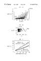
- FIG. 6Ashows the electron emission current vs. applied voltage for anode-cathode distances from 6.6 ⁇ m to 320.1 ⁇ m, for the iron-coated sample. It is clear that smooth and consistent I-V curves are measured in a history-independent, reproducible manner.
- FIG. 6Bshows the same data as FIG. 6A, but is plotted as log(I/V 2 ) vs. 1/V, which shows the characteristic Fowler-Nordheim linearity.
- FIG. 7shows that for the iron-coated sample, the turn-on field (i.e., the field that generates an emission current of 1 nA) is only 1.7 V/ ⁇ m, and the threshold field (i.e., the field that generates an emission current density of 10 mA/cm 2 ) is 2.8 V/ ⁇ m.
- the turn-on fieldi.e., the field that generates an emission current of 1 nA
- the threshold fieldi.e., the field that generates an emission current density of 10 mA/cm 2
- X-ray diffraction patternswere obtained for both stretched and nonstretched samples, using a 1.5 kW Cu source, HOPG (002) monochromator, and a two dimensional imaging plate detector (MAC Science DIP2000 with 2500 ⁇ 2500 pixels and 80 ⁇ m pixel resolution) in the transmission mode. Structures of multi-walled nanotubes have been previously studied. (See, e.g., O. Zhou et al., Science, Vol. 263, 1744 (1994). The diffraction pattern is dominated by a strong Bragg peak centered around 3.4 ⁇ , which corresponds to the inter-shell spacing within the same nanotube (referred to as the (002) peak).
- the x-ray diffraction pattern of a stretched (330%) film having about 50 wt. % nanotubesis shown in FIG. 8 B.
- the datawas taken with K i perpendicular to the film surface and stretching direction.
- the change in diffraction pattern from FIG. 8Ashows that the nanotubes in the stretched film are aligned with their longitudinal axes parallel to the stretching direction.
- the fraction of nanotubes aligned, and the degree of alignmentare capable of being determined.
- 58% of the nanotubeswere substantially aligned along the stress direction, with a cone of 20° mosaic angle.
- the dispersion and alignment of the nanotubeswere examined by transmission electron microscopy (TEM).
- TEMtransmission electron microscopy
- the composite sampleswere cut into approximately 90 nm thick membranes using microtomy with a diamond blade.
- the nanotubes and impurity nanoparticleswere dispersed in the matrix without significant aggregation, and were substantially wetted by the polymer, as reflected in FIG. 5, which shows a film sample that was sliced parallel to the stretching direction (indicated by the arrows).
Landscapes
- Engineering & Computer Science (AREA)
- Chemical & Material Sciences (AREA)
- Manufacturing & Machinery (AREA)
- Nanotechnology (AREA)
- Crystallography & Structural Chemistry (AREA)
- Organic Chemistry (AREA)
- Inorganic Chemistry (AREA)
- Cold Cathode And The Manufacture (AREA)
- Carbon And Carbon Compounds (AREA)
- Micromachines (AREA)
- Application Of Or Painting With Fluid Materials (AREA)
- Electrodes For Cathode-Ray Tubes (AREA)
- Cathode-Ray Tubes And Fluorescent Screens For Display (AREA)
- Electrodes Of Semiconductors (AREA)
- Microwave Amplifiers (AREA)
Abstract
Description
Claims (17)
Priority Applications (7)
| Application Number | Priority Date | Filing Date | Title |
|---|---|---|---|
| US09/296,572US6630772B1 (en) | 1998-09-21 | 1999-04-22 | Device comprising carbon nanotube field emitter structure and process for forming device |
| EP99307243AEP0989579B1 (en) | 1998-09-21 | 1999-09-14 | Device comprising a carbon nanotube field emitter structure and process for forming device |
| DE69939965TDE69939965D1 (en) | 1998-09-21 | 1999-09-14 | Arrangement with a carbon nanotube field emission structure and manufacturing method |
| JP26610399AJP2000141056A (en) | 1998-09-21 | 1999-09-20 | Device having adhesive carbon nano-tube film |
| KR1019990040668AKR100768675B1 (en) | 1998-09-21 | 1999-09-21 | Device comprising a carbon nanotube field emitter structure and method of forming the device |
| JP2004302950AJP4021889B2 (en) | 1998-09-21 | 2004-10-18 | Carbon nanotube film device manufacturing method |
| JP2007162461AJP2007287699A (en) | 1998-09-21 | 2007-06-20 | Method for manufacturing carbon nanotube film device |
Applications Claiming Priority (2)
| Application Number | Priority Date | Filing Date | Title |
|---|---|---|---|
| US10120398P | 1998-09-21 | 1998-09-21 | |
| US09/296,572US6630772B1 (en) | 1998-09-21 | 1999-04-22 | Device comprising carbon nanotube field emitter structure and process for forming device |
Publications (1)
| Publication Number | Publication Date |
|---|---|
| US6630772B1true US6630772B1 (en) | 2003-10-07 |
Family
ID=26798011
Family Applications (1)
| Application Number | Title | Priority Date | Filing Date |
|---|---|---|---|
| US09/296,572Expired - LifetimeUS6630772B1 (en) | 1998-09-21 | 1999-04-22 | Device comprising carbon nanotube field emitter structure and process for forming device |
Country Status (5)
| Country | Link |
|---|---|
| US (1) | US6630772B1 (en) |
| EP (1) | EP0989579B1 (en) |
| JP (3) | JP2000141056A (en) |
| KR (1) | KR100768675B1 (en) |
| DE (1) | DE69939965D1 (en) |
Cited By (220)
| Publication number | Priority date | Publication date | Assignee | Title |
|---|---|---|---|---|
| US20020035170A1 (en)* | 1999-02-12 | 2002-03-21 | Paul Glatkowski | Electromagnetic shielding composite comprising nanotubes |
| US20020048632A1 (en)* | 2000-08-24 | 2002-04-25 | Smalley Richard E. | Polymer-wrapped single wall carbon nanotubes |
| US20020074932A1 (en)* | 2000-06-21 | 2002-06-20 | Bouchard Robert Joseph | Process for improving the emission of electron field emitters |
| US20020119724A1 (en)* | 1999-10-15 | 2002-08-29 | Electrovac, Fabrikation Electrotechnischer Spezialartikel Gesellschaft Mbh | Method for producing a field emission display |
| US20020179434A1 (en)* | 1998-08-14 | 2002-12-05 | The Board Of Trustees Of The Leland Stanford Junior University | Carbon nanotube devices |
| US20020197752A1 (en)* | 1999-05-24 | 2002-12-26 | Choi Won-Bong | Carbon nanotube field emission array and method for fabricating the same |
| US20030044519A1 (en)* | 2001-06-14 | 2003-03-06 | Hyperion Catalysis International, Inc. | Field emission devices using ion bombarded carbon nanotubes |
| US20030041438A1 (en)* | 2001-08-28 | 2003-03-06 | Motorola, Inc. | Vacuum microelectronic device |
| US20030048055A1 (en)* | 2001-09-10 | 2003-03-13 | Junri Ishikura | Manufacture method for electron-emitting device, electron source, light-emitting apparatus, and image forming apparatus |
| US20030092207A1 (en)* | 2001-10-19 | 2003-05-15 | Zvi Yaniv | Activation effect on carbon nanotubes |
| US20030111333A1 (en)* | 2001-12-17 | 2003-06-19 | Intel Corporation | Method and apparatus for producing aligned carbon nanotube thermal interface structure |
| US20030132393A1 (en)* | 2000-02-16 | 2003-07-17 | Steven Dimitrijevic | Diamond/carbon nanotube structures for efficient electron field emission |
| US20030148577A1 (en)* | 2002-02-06 | 2003-08-07 | Merkulov Vladimir I. | Controlled alignment of catalytically grown nanostructures in a large-scale synthesis process |
| US20030197458A1 (en)* | 2002-04-19 | 2003-10-23 | Mitsubishi Pencil Co., Ltd. | Electrode for electron gun and electron gun using same |
| US20040013597A1 (en)* | 2002-04-12 | 2004-01-22 | Si Diamond Technology, Inc. | Metallization of carbon nanotubes for field emission applications |
| US20040032194A1 (en)* | 2002-08-09 | 2004-02-19 | Matsushita Electric Industrial Co., Ltd. | Field-emission electron source element and image display apparatus |
| US20040038614A1 (en)* | 2002-08-24 | 2004-02-26 | Yu-Yang Chang | Method of growing isomeric carbon emitters onto triode structure of field emission display |
| US20040051432A1 (en)* | 2002-09-16 | 2004-03-18 | Jiang Kaili | Light filament formed from carbon nanotubes and method for making same |
| WO2003099709A3 (en)* | 2002-05-21 | 2004-03-18 | Eikos Inc | Method for patterning carbon nanotube coating and carbon nanotube wiring |
| US20040055892A1 (en)* | 2001-11-30 | 2004-03-25 | University Of North Carolina At Chapel Hill | Deposition method for nanostructure materials |
| US20040099208A1 (en)* | 2002-11-22 | 2004-05-27 | Kang Sung Gu | Method for forming carbon nanotubes |
| US20040108298A1 (en)* | 2002-07-03 | 2004-06-10 | Applied Nanotechnologies, Inc. | Fabrication and activation processes for nanostructure composite field emission cathodes |
| US20040114721A1 (en)* | 2000-10-06 | 2004-06-17 | Applied Nanotechnologies, Inc. | Devices and methods for producing multiple x-ray beams from multiple locations |
| US6780664B1 (en)* | 2002-12-20 | 2004-08-24 | Advanced Micro Devices, Inc. | Nanotube tip for atomic force microscope |
| US20040173378A1 (en)* | 2002-12-09 | 2004-09-09 | University Of North Carolina At Chapel Hill | Methods for assembly and sorting of nanostructure-containing materials and related articles |
| US20040192151A1 (en)* | 2003-03-25 | 2004-09-30 | Canon Kabushiki Kaisha | Methods for severally manufacturing carbon fibers, electron-emitting device, electron source, image display apparatus, light bulb, and secondary battery |
| US20040223381A1 (en)* | 2000-12-08 | 2004-11-11 | Nano-Proprietary, Inc. | Low work function material |
| US20040228961A1 (en)* | 2002-12-04 | 2004-11-18 | United States Of America As Represented By The Admin. Of The Nat'l Aeronautics & Space Admin. | Controlled deposition and alignment of carbon nanotubes |
| US20040240616A1 (en)* | 2003-05-30 | 2004-12-02 | Applied Nanotechnologies, Inc. | Devices and methods for producing multiple X-ray beams from multiple locations |
| US20040241896A1 (en)* | 2003-03-21 | 2004-12-02 | The University Of North Carolina At Chapel Hill | Methods and apparatus for patterned deposition of nanostructure-containing materials by self-assembly and related articles |
| US20040250753A1 (en)* | 2002-11-22 | 2004-12-16 | Kang Sung Gu | Method for forming carbon nanotubes with post-treatment step |
| US20040256975A1 (en)* | 2003-06-19 | 2004-12-23 | Applied Nanotechnologies, Inc. | Electrode and associated devices and methods |
| US20040261987A1 (en)* | 2003-06-30 | 2004-12-30 | Yuegang Zhang | Thermal interface apparatus, systems, and methods |
| US20050009350A1 (en)* | 2003-07-08 | 2005-01-13 | Mirko Vogt | Carbon hard mask with bonding layer for bonding to metal |
| US20050058590A1 (en)* | 2003-09-08 | 2005-03-17 | Nantero, Inc. | Spin-coatable liquid for formation of high purity nanotube films |
| US20050065741A1 (en)* | 2003-05-14 | 2005-03-24 | Nantero, Inc. | Sensor platform using a non-horizontally oriented nanotube element |
| US20050089638A1 (en)* | 2003-09-16 | 2005-04-28 | Koila, Inc. | Nano-material thermal and electrical contact system |
| US20050101112A1 (en)* | 2001-07-25 | 2005-05-12 | Nantero, Inc. | Methods of nanotubes films and articles |
| US20050099111A1 (en)* | 2002-09-17 | 2005-05-12 | Masaaki Hirakawa | Method for the preparation of graphite nanofibers and emitter and display elements comprising the nanofibers |
| US20050133372A1 (en)* | 2001-11-30 | 2005-06-23 | The University Of North Carolina | Method and apparatus for attaching nanostructure-containing material onto a sharp tip of an object and related articles |
| US20050132949A1 (en)* | 2002-11-22 | 2005-06-23 | Kang Sung G. | Forming carbon nanotubes by iterating nanotube growth and post-treatment steps |
| US20050139991A1 (en)* | 2003-12-30 | 2005-06-30 | Intel Corporation | Thermal intermediate apparatus, systems, and methods |
| US20050139642A1 (en)* | 2003-12-30 | 2005-06-30 | Intel Corporation | Nanotube modified solder thermal intermediate structure, systems, and methods |
| US20050164583A1 (en)* | 1999-11-26 | 2005-07-28 | Geohegan David B. | Condensed phase conversion and growth of nanorods and other materials instead of from vapor |
| US20050170169A1 (en)* | 2003-10-09 | 2005-08-04 | Fuji Xerox Co., Ltd. | Composite and method of manufacturing the same |
| US20050169830A1 (en)* | 1999-10-27 | 2005-08-04 | William Marsh Rice University | Macroscopic ordered assembly of carbon nanotubes |
| US20050202578A1 (en)* | 2001-10-19 | 2005-09-15 | Nano-Proprietary, Inc. | Ink jet application for carbon nanotubes |
| US20050224764A1 (en)* | 2002-06-14 | 2005-10-13 | Hyperion Catalysis International, Inc. | Electroconductive carbon fibril-based inks snd coatings |
| US20050226361A1 (en)* | 2000-10-06 | 2005-10-13 | The University Of North Carolina At Chapel Hill | Computed tomography scanning system and method using a field emission x-ray source |
| US20050241765A1 (en)* | 2004-04-30 | 2005-11-03 | Rajinder Dhindsa | Apparatus including showerhead electrode and heater for plasma processing |
| US20050241766A1 (en)* | 2004-04-30 | 2005-11-03 | Rajinder Dhindsa | Apparatus including gas distribution member supplying process gas and radio frequency (RF) power for plasma processing |
| US20050269553A1 (en)* | 2003-09-08 | 2005-12-08 | Nantero, Inc. | Spin-coatable liquid for use in electronic fabrication processes |
| US6979947B2 (en)* | 2002-07-09 | 2005-12-27 | Si Diamond Technology, Inc. | Nanotriode utilizing carbon nanotubes and fibers |
| US20060008047A1 (en)* | 2000-10-06 | 2006-01-12 | The University Of North Carolina At Chapel Hill | Computed tomography system for imaging of human and small animal |
| US6987071B1 (en)* | 2003-11-21 | 2006-01-17 | Nanosolar, Inc. | Solvent vapor infiltration of organic materials into nanostructures |
| US20060018432A1 (en)* | 2000-10-06 | 2006-01-26 | The University Of North Carolina At Chapel Hill | Large-area individually addressable multi-beam x-ray system and method of forming same |
| US20060038167A1 (en)* | 2004-08-20 | 2006-02-23 | International Business Machines Corporation | Integrated carbon nanotube sensors |
| US20060046602A1 (en)* | 2004-08-30 | 2006-03-02 | Samsung Electro-Mechanics Co., Ltd. | Method of manufacturing field emitter electrode using self-assembling carbon nanotubes and field emitter electrode manufactured thereby |
| US20060049743A1 (en)* | 2004-08-23 | 2006-03-09 | Makoto Okai | Flat panel display |
| US20060057927A1 (en)* | 2004-09-14 | 2006-03-16 | Samsung Electro-Mechanics Co., Ltd. | Fabrication method of field emitter electrode |
| US20060066202A1 (en)* | 2004-05-27 | 2006-03-30 | Manohara Harish M | Carbon nanotube high-current-density field emitters |
| US7026432B2 (en) | 2003-08-12 | 2006-04-11 | General Electric Company | Electrically conductive compositions and method of manufacture thereof |
| US20060135030A1 (en)* | 2004-12-22 | 2006-06-22 | Si Diamond Technology,Inc. | Metallization of carbon nanotubes for field emission applications |
| US20060151777A1 (en)* | 2005-01-12 | 2006-07-13 | Naberhuis Steven L | Multi-layer thin film in a ballistic electron emitter |
| US20060192494A1 (en)* | 2005-02-25 | 2006-08-31 | Mastroianni Sal T | In-situ sealed carbon nanotube vacuum device |
| US20060193093A1 (en)* | 2004-11-02 | 2006-08-31 | Nantero, Inc. | Nanotube ESD protective devices and corresponding nonvolatile and volatile nanotube switches |
| US20060199002A1 (en)* | 2005-03-02 | 2006-09-07 | Cabot Microelectronics Corporation | Method of preparing a conductive film |
| US20060196537A1 (en)* | 2005-03-02 | 2006-09-07 | Wisconsin Alumni Research Foundation | Carbon nanotube schottky barrier photovoltaic cell |
| US20060258122A1 (en)* | 2005-05-12 | 2006-11-16 | Whitefield Bruce J | Nanotube fuse structure |
| US20060261719A1 (en)* | 2003-08-29 | 2006-11-23 | Neil Fox | Field emitter device |
| US20060260785A1 (en)* | 2005-05-13 | 2006-11-23 | Delta Electronics, Inc. | Heat sink |
| US20060274889A1 (en)* | 2000-10-06 | 2006-12-07 | University Of North Carolina At Chapel Hill | Method and apparatus for controlling electron beam current |
| US20060281256A1 (en)* | 2005-06-08 | 2006-12-14 | Carter Richard J | Self-aligned cell integration scheme |
| US20060284538A1 (en)* | 2005-06-17 | 2006-12-21 | Avetik Harutyunyan | Carbon single-walled nanotubes as electrodes for electrochromic glasses |
| US20070004191A1 (en)* | 2005-06-30 | 2007-01-04 | Lsi Logic Corporation | Novel techniques for precision pattern transfer of carbon nanotubes from photo mask to wafers |
| KR100665881B1 (en) | 2005-12-30 | 2007-01-09 | 한국전기연구원 | Cathode module for electron beam generation of carbon nanotube based X-ray tube |
| US20070014148A1 (en)* | 2004-05-10 | 2007-01-18 | The University Of North Carolina At Chapel Hill | Methods and systems for attaching a magnetic nanowire to an object and apparatuses formed therefrom |
| US20070036709A1 (en)* | 2005-07-28 | 2007-02-15 | Lashmore David S | Systems and methods for formation and harvesting of nanofibrous materials |
| US20070053489A1 (en)* | 2005-04-25 | 2007-03-08 | The University Of North Carolina At Chapel Hill | X-ray imaging systems and methods using temporal digital signal processing for reducing noise and for obtaining multiple images simultaneously |
| US20070063630A1 (en)* | 2005-09-22 | 2007-03-22 | Tsinghua University | Field emission cathode and planar light source using the same |
| US20070081681A1 (en)* | 2005-10-03 | 2007-04-12 | Xun Yu | Thin film transparent acoustic transducer |
| US7220971B1 (en) | 2004-12-29 | 2007-05-22 | The University Of North Carolina At Chapel Hill | Multi-pixel electron microbeam irradiator systems and methods for selectively irradiating predetermined locations |
| US7241496B2 (en) | 2002-05-02 | 2007-07-10 | Zyvex Performance Materials, LLC. | Polymer and method for using the polymer for noncovalently functionalizing nanotubes |
| US20070161261A1 (en)* | 2006-01-11 | 2007-07-12 | Industrial Technology Research Institute | Methods for fabricating carbon nano-tube powders and field emission display devices |
| US20070158768A1 (en)* | 2006-01-06 | 2007-07-12 | Honeywell International, Inc. | Electrical contacts formed of carbon nanotubes |
| US7244407B2 (en) | 2002-05-02 | 2007-07-17 | Zyvex Performance Materials, Llc | Polymer and method for using the polymer for solubilizing nanotubes |
| US7259510B1 (en)* | 2000-08-30 | 2007-08-21 | Agere Systems Inc. | On-chip vacuum tube device and process for making device |
| US20070206726A1 (en)* | 2005-11-17 | 2007-09-06 | Xintek, Inc. | Systems and methods for x-ray imaging and scanning of objects |
| US7274078B2 (en) | 2001-07-25 | 2007-09-25 | Nantero, Inc. | Devices having vertically-disposed nanofabric articles and methods of making the same |
| US20070243717A1 (en)* | 2004-11-29 | 2007-10-18 | Francisco Santiago | Carbon nanotube apparatus and method of carbon nanotube modification |
| US7296576B2 (en) | 2004-08-18 | 2007-11-20 | Zyvex Performance Materials, Llc | Polymers for enhanced solubility of nanomaterials, compositions and methods therefor |
| US20070275627A1 (en)* | 2006-05-26 | 2007-11-29 | Korea Advanced Institute Of Science And Technology | Method for fabricating field emitter electrode using array of carbon nanotubes |
| US7304357B2 (en) | 2001-07-25 | 2007-12-04 | Nantero, Inc. | Devices having horizontally-disposed nanofabric articles and methods of making the same |
| US20070278925A1 (en)* | 2004-09-10 | 2007-12-06 | Nano-Proprietary, Inc. | Enhanced electron field emission from carbon nanotubes without activation |
| US7309727B2 (en) | 2003-09-29 | 2007-12-18 | General Electric Company | Conductive thermoplastic compositions, methods of manufacture and articles derived from such compositions |
| US20080003801A1 (en)* | 2003-02-03 | 2008-01-03 | Dubin Valery M | Packaging of integrated circuits with carbon nano-tube arrays to enhance heat dissipation through a thermal interface |
| US7335395B2 (en)* | 2002-04-23 | 2008-02-26 | Nantero, Inc. | Methods of using pre-formed nanotubes to make carbon nanotube films, layers, fabrics, ribbons, elements and articles |
| US7342818B2 (en) | 2001-07-25 | 2008-03-11 | Nantero, Inc. | Hybrid circuit having nanotube electromechanical memory |
| US7344691B2 (en) | 2001-05-17 | 2008-03-18 | Zyvek Performance Materials, Llc | System and method for manipulating nanotubes |
| US20080079027A1 (en)* | 2004-06-09 | 2008-04-03 | Nantero, Inc. | Field effect devices having a gate controlled via a nanotube switching element |
| US7354988B2 (en) | 2003-08-12 | 2008-04-08 | General Electric Company | Electrically conductive compositions and method of manufacture thereof |
| US20080142850A1 (en)* | 2005-05-09 | 2008-06-19 | Nantero, Inc. | Memory elements and cross point switches and arrays of same using nonvolatile nanotube blocks |
| US20080157257A1 (en)* | 2005-05-09 | 2008-07-03 | Nantero, Inc. | Nonvolatile nanotube diodes and nonvolatile nanotube blocks and systems using same and methods of making same |
| US20080157127A1 (en)* | 2005-05-09 | 2008-07-03 | Nantero, Inc. | Nonvolatile nanotube diodes and nonvolatile nanotube blocks and systems using same and methods of making same |
| WO2008094888A1 (en)* | 2007-01-30 | 2008-08-07 | Steffen Mckernan | Fabrication process for nanotube-cmos integration |
| US20080199626A1 (en)* | 2002-03-25 | 2008-08-21 | University Of North Carolina At Chapel Hill | Method for assembling nano objects |
| DE102007039904A1 (en)* | 2007-08-23 | 2008-08-28 | Siemens Ag | Heat-conductive material layer manufacturing method, involves inserting fibers in field area and transporting towards carrier layer, where fibers have large heat-conductivity toward fiber longitudinal direction than other direction |
| US20080203886A1 (en)* | 2001-06-14 | 2008-08-28 | Hyperion Catalysis International, Inc. | Field emission devices using modified carbon nanotubes |
| US20080212361A1 (en)* | 2005-05-09 | 2008-09-04 | Nantero, Inc. | Nonvolatile nanotube diodes and nonvolatile nanotube blocks and systems using same and methods of making same |
| US20080227360A1 (en)* | 2006-11-24 | 2008-09-18 | Tsinghua University | Method for fabricating electron emitter |
| US20080231413A1 (en)* | 2004-09-21 | 2008-09-25 | Nantero, Inc. | Resistive elements using carbon nanotubes |
| US20080238882A1 (en)* | 2007-02-21 | 2008-10-02 | Ramesh Sivarajan | Symmetric touch screen system with carbon nanotube-based transparent conductive electrode pairs |
| USD578536S1 (en)* | 2007-08-27 | 2008-10-14 | Podium Photonics (Guangzhou) Ltd. | Chip |
| US20080280038A1 (en)* | 2003-01-13 | 2008-11-13 | Nantero, Inc. | Methods of using thin metal layers to make carbon nanotube films, layers, fabrics, ribbons, elements and articles |
| US20080292979A1 (en)* | 2007-05-22 | 2008-11-27 | Zhe Ding | Transparent conductive materials and coatings, methods of production and uses thereof |
| US7462656B2 (en) | 2005-02-15 | 2008-12-09 | Sabic Innovative Plastics Ip B.V. | Electrically conductive compositions and method of manufacture thereof |
| US20080302385A1 (en)* | 2004-04-15 | 2008-12-11 | Kenji Nakamura | Cosmetic tool having antibacterial property and method for producing the same |
| US7479516B2 (en) | 2003-05-22 | 2009-01-20 | Zyvex Performance Materials, Llc | Nanocomposites and methods thereto |
| US20090022977A1 (en)* | 2007-07-20 | 2009-01-22 | Usa As Represented By The Administrator Of The National Aeronautics And Space Administration | Combination structural support and thermal protection system |
| US20090022264A1 (en)* | 2007-07-19 | 2009-01-22 | Zhou Otto Z | Stationary x-ray digital breast tomosynthesis systems and related methods |
| US20090035707A1 (en)* | 2007-08-01 | 2009-02-05 | Yubing Wang | Rheology-controlled conductive materials, methods of production and uses thereof |
| US20090051032A1 (en)* | 2003-09-08 | 2009-02-26 | Segal Brent M | Patterned nanoscopic articles and methods of making the same |
| WO2008157509A3 (en)* | 2007-06-14 | 2009-02-26 | Univ Florida | Room temperature carbon nanotubes integrated on cmos |
| US20090061550A1 (en)* | 2005-07-20 | 2009-03-05 | Samsung Electro-Mechanics Co., Ltd. | Led package and fabricating method thereof |
| US20090056589A1 (en)* | 2007-08-29 | 2009-03-05 | Honeywell International, Inc. | Transparent conductors having stretched transparent conductive coatings and methods for fabricating the same |
| CN100468601C (en)* | 2004-05-25 | 2009-03-11 | 东元奈米应材股份有限公司 | Electron emission source for field emission display and method of fabricating the same |
| US20090078914A1 (en)* | 2007-09-20 | 2009-03-26 | Xintek, Inc. | Methods and devices for electrophoretic deposition of a uniform carbon nanotube composite film |
| US20090087622A1 (en)* | 2005-12-01 | 2009-04-02 | Ahmed Busnaina | Directed Assembly of Carbon Nanotubes and Nanoparticles Using Nanotemplates With Nanotrenches |
| US20090099016A1 (en)* | 2005-12-19 | 2009-04-16 | Advanced Technology Materials, Inc. | Production of carbon nanotubes |
| US20090115305A1 (en)* | 2007-05-22 | 2009-05-07 | Nantero, Inc. | Triodes using nanofabric articles and methods of making the same |
| US20090140167A1 (en)* | 2005-09-06 | 2009-06-04 | Natero, Inc. | Nanotube fabric-based sensor systems and methods of making same |
| US7556746B2 (en) | 2004-06-03 | 2009-07-07 | Nantero, Inc. | Method of making an applicator liquid for electronics fabrication process |
| US20090173964A1 (en)* | 2001-07-25 | 2009-07-09 | Nantero, Inc. | Method of forming a carbon nanotube-based contact to semiconductor |
| US7560136B2 (en) | 2003-01-13 | 2009-07-14 | Nantero, Inc. | Methods of using thin metal layers to make carbon nanotube films, layers, fabrics, ribbons, elements and articles |
| US20090184389A1 (en)* | 2005-05-09 | 2009-07-23 | Bertin Claude L | Nonvolatile Nanotube Diodes and Nonvolatile Nanotube Blocks and Systems Using Same and Methods of Making Same |
| US7566478B2 (en) | 2001-07-25 | 2009-07-28 | Nantero, Inc. | Methods of making carbon nanotube films, layers, fabrics, ribbons, elements and articles |
| US20090189124A1 (en)* | 2008-01-28 | 2009-07-30 | Honeywell International, Inc. | Transparent conductors and methods for fabricating transparent conductors |
| US20090188697A1 (en)* | 2008-01-28 | 2009-07-30 | Honeywell International, Inc. | Transparent conductors and methods for fabricating transparent conductors |
| US20090194839A1 (en)* | 2005-11-15 | 2009-08-06 | Bertin Claude L | Nonvolatile nanotube diodes and nonvolatile nanotube blocks and systems using same and methods of making same |
| US20090195138A1 (en)* | 2008-02-01 | 2009-08-06 | Tsinghua University | Electron emission device and display device using the same |
| US20090224680A1 (en)* | 2008-03-04 | 2009-09-10 | Pan David H | Field emission light emitting device |
| US20090237886A1 (en)* | 2008-03-18 | 2009-09-24 | Fujitsu Limited | Sheet structure and method of manufacturing sheet structure |
| US20090256463A1 (en)* | 2008-04-09 | 2009-10-15 | Tsinghua University | Electron emission device and display device using the same |
| US20090256462A1 (en)* | 2008-04-09 | 2009-10-15 | Tsinghua University | Electron emission device and display device using the same |
| US20090302738A1 (en)* | 2008-06-06 | 2009-12-10 | Xerox Corporation | Field emission light emitting device |
| US20100001267A1 (en)* | 2008-06-20 | 2010-01-07 | Nantero, Inc. | Nram arrays with nanotube blocks, nanotube traces, and nanotube planes and methods of making same |
| US20100012927A1 (en)* | 2001-07-25 | 2010-01-21 | Nantero, Inc. | Devices having vertically-disposed nanofabric articles and methods of making the same |
| US7658869B2 (en) | 2004-06-03 | 2010-02-09 | Nantero, Inc. | Applicator liquid containing ethyl lactate for preparation of nanotube films |
| US20100038595A1 (en)* | 2005-02-04 | 2010-02-18 | Imholt Timothy J | System and methods of dispersion of nanostructures in composite materials |
| US7666382B2 (en) | 2004-12-16 | 2010-02-23 | Nantero, Inc. | Aqueous carbon nanotube applicator liquids and methods for producing applicator liquids thereof |
| US7727578B2 (en) | 2007-12-27 | 2010-06-01 | Honeywell International Inc. | Transparent conductors and methods for fabricating transparent conductors |
| US20100147657A1 (en)* | 2004-11-02 | 2010-06-17 | Nantero, Inc. | Nanotube esd protective devices and corresponding nonvolatile and volatile nanotube switches |
| US7745810B2 (en) | 2001-07-25 | 2010-06-29 | Nantero, Inc. | Nanotube films and articles |
| US7744793B2 (en) | 2005-09-06 | 2010-06-29 | Lemaire Alexander B | Apparatus and method for growing fullerene nanotube forests, and forming nanotube films, threads and composite structures therefrom |
| US20100164355A1 (en)* | 2008-12-26 | 2010-07-01 | Samsung Electronics Co., Ltd. | Field emission device and method of manufacturing the same |
| US7781862B2 (en) | 2005-05-09 | 2010-08-24 | Nantero, Inc. | Two-terminal nanotube devices and systems and methods of making same |
| US20100267205A1 (en)* | 2005-09-06 | 2010-10-21 | Lockheed Martin Corporation | Carbon nanotubes for the selective transfer of heat from electronics |
| CN1962427B (en)* | 2005-11-09 | 2010-11-10 | 鸿富锦精密工业(深圳)有限公司 | Production method of nano-carbon tube |
| US7858185B2 (en) | 2003-09-08 | 2010-12-28 | Nantero, Inc. | High purity nanotube fabrics and films |
| US20100327247A1 (en)* | 2005-09-06 | 2010-12-30 | Nantero, Inc. | Method and system of using nanotube fabrics as joule heating elements for memories and other applications |
| US20110027497A1 (en)* | 2009-07-31 | 2011-02-03 | Nantero, Inc. | Anisotropic nanotube fabric layers and films and methods of forming same |
| US20110034008A1 (en)* | 2009-08-07 | 2011-02-10 | Nantero, Inc. | Method for forming a textured surface on a semiconductor substrate using a nanofabric layer |
| US7915637B2 (en) | 2008-11-19 | 2011-03-29 | Nantero, Inc. | Switching materials comprising mixed nanoscopic particles and carbon nanotubes and method of making and using the same |
| US20110117582A1 (en)* | 2005-12-01 | 2011-05-19 | Northeastern University | Multi-biomarker biosensor |
| US20110156009A1 (en)* | 2009-12-31 | 2011-06-30 | Manning H Montgomery | Compact electrical switching devices with nanotube elements, and methods of making same |
| US20110163290A1 (en)* | 2009-10-23 | 2011-07-07 | Nantero, Inc. | Methods for passivating a carbonic nanolayer |
| US20110203632A1 (en)* | 2010-02-22 | 2011-08-25 | Rahul Sen | Photovoltaic devices using semiconducting nanotube layers |
| US20110220172A1 (en)* | 2007-11-06 | 2011-09-15 | Pacific Integrated Energy, Inc. | Photo induced enhanced field electron emission collector |
| US20110318485A1 (en)* | 2010-06-29 | 2011-12-29 | Hon Hai Precision Industry Co., Ltd. | Method for making composite carbon nanotube structure |
| US8110883B2 (en) | 2007-03-12 | 2012-02-07 | Nantero Inc. | Electromagnetic and thermal sensors using carbon nanotubes and methods of making same |
| US8155262B2 (en) | 2005-04-25 | 2012-04-10 | The University Of North Carolina At Chapel Hill | Methods, systems, and computer program products for multiplexing computed tomography |
| US8189893B2 (en) | 2006-05-19 | 2012-05-29 | The University Of North Carolina At Chapel Hill | Methods, systems, and computer program products for binary multiplexing x-ray radiography |
| US8217490B2 (en) | 2005-05-09 | 2012-07-10 | Nantero Inc. | Nonvolatile nanotube diodes and nonvolatile nanotube blocks and systems using same and methods of making same |
| CN1705059B (en)* | 2004-05-26 | 2012-08-29 | 清华大学 | Carbon nano tube field emission device and preparation method thereof |
| US8273486B2 (en) | 2009-01-30 | 2012-09-25 | Honeywell International, Inc. | Protecting a PEM fuel cell catalyst against carbon monoxide poisoning |
| US20120273124A1 (en)* | 2007-12-14 | 2012-11-01 | Hon Hai Precision Industry Co., Ltd. | Method for making touch panel |
| US20120279052A1 (en)* | 2007-12-14 | 2012-11-08 | Hon Hai Precision Industry Co., Ltd. | Method for making touch panel |
| US8351239B2 (en) | 2009-10-23 | 2013-01-08 | Nantero Inc. | Dynamic sense current supply circuit and associated method for reading and characterizing a resistive memory array |
| US8358739B2 (en) | 2010-09-03 | 2013-01-22 | The University Of North Carolina At Chapel Hill | Systems and methods for temporal multiplexing X-ray imaging |
| US8471238B2 (en) | 2004-09-16 | 2013-06-25 | Nantero Inc. | Light emitters using nanotubes and methods of making same |
| US8513768B2 (en) | 2005-05-09 | 2013-08-20 | Nantero Inc. | Nonvolatile nanotube diodes and nonvolatile nanotube blocks and systems using same and methods of making same |
| US8574673B2 (en) | 2009-07-31 | 2013-11-05 | Nantero Inc. | Anisotropic nanotube fabric layers and films and methods of forming same |
| US8580586B2 (en) | 2005-05-09 | 2013-11-12 | Nantero Inc. | Memory arrays using nanotube articles with reprogrammable resistance |
| US8600003B2 (en) | 2009-01-16 | 2013-12-03 | The University Of North Carolina At Chapel Hill | Compact microbeam radiation therapy systems and methods for cancer treatment and research |
| US8636972B1 (en) | 2007-07-31 | 2014-01-28 | Raytheon Company | Making a nanomaterial composite |
| US8895950B2 (en) | 2009-10-23 | 2014-11-25 | Nantero Inc. | Methods for passivating a carbonic nanolayer |
| US20140361225A1 (en)* | 2012-03-08 | 2014-12-11 | Tsinghua University | Method for making carbon nanotube slurry |
| US8937575B2 (en) | 2009-07-31 | 2015-01-20 | Nantero Inc. | Microstrip antenna elements and arrays comprising a shaped nanotube fabric layer and integrated two terminal nanotube select devices |
| US8941094B2 (en) | 2010-09-02 | 2015-01-27 | Nantero Inc. | Methods for adjusting the conductivity range of a nanotube fabric layer |
| US9053890B2 (en) | 2013-08-02 | 2015-06-09 | University Health Network | Nanostructure field emission cathode structure and method for making |
| US9136794B2 (en) | 2011-06-22 | 2015-09-15 | Research Triangle Institute, International | Bipolar microelectronic device |
| US9156698B2 (en) | 2012-02-29 | 2015-10-13 | Yazaki Corporation | Method of purifying carbon nanotubes and applications thereof |
| US9198232B2 (en) | 2008-05-07 | 2015-11-24 | Nanocomp Technologies, Inc. | Nanostructure-based heating devices and methods of use |
| US9214332B2 (en) | 2014-03-20 | 2015-12-15 | International Business Machines Corporation | Composite dielectric materials with improved mechanical and electrical properties |
| US9299430B1 (en) | 2015-01-22 | 2016-03-29 | Nantero Inc. | Methods for reading and programming 1-R resistive change element arrays |
| US9348078B2 (en) | 2010-06-08 | 2016-05-24 | Pacific Integrated Energy, Inc. | Optical antennas with enhanced fields and electron emission |
| US9422651B2 (en) | 2003-01-13 | 2016-08-23 | Nantero Inc. | Methods for arranging nanoscopic elements within networks, fabrics, and films |
| US9574290B2 (en) | 2003-01-13 | 2017-02-21 | Nantero Inc. | Methods for arranging nanotube elements within nanotube fabrics and films |
| US9617151B2 (en) | 2010-02-12 | 2017-04-11 | Nantero Inc. | Methods for controlling density, porosity, and/or gap size within nanotube fabric layers and films |
| US9650732B2 (en) | 2013-05-01 | 2017-05-16 | Nantero Inc. | Low defect nanotube application solutions and fabrics and methods for making same |
| US9718691B2 (en) | 2013-06-17 | 2017-08-01 | Nanocomp Technologies, Inc. | Exfoliating-dispersing agents for nanotubes, bundles and fibers |
| US9782136B2 (en) | 2014-06-17 | 2017-10-10 | The University Of North Carolina At Chapel Hill | Intraoral tomosynthesis systems, methods, and computer readable media for dental imaging |
| US9911743B2 (en) | 2005-05-09 | 2018-03-06 | Nantero, Inc. | Nonvolatile nanotube diodes and nonvolatile nanotube blocks and systems using same and methods of making same |
| US9934848B2 (en) | 2016-06-07 | 2018-04-03 | Nantero, Inc. | Methods for determining the resistive states of resistive change elements |
| US9941001B2 (en) | 2016-06-07 | 2018-04-10 | Nantero, Inc. | Circuits for determining the resistive states of resistive change elements |
| US10355206B2 (en) | 2017-02-06 | 2019-07-16 | Nantero, Inc. | Sealed resistive change elements |
| WO2019190635A1 (en)* | 2018-03-30 | 2019-10-03 | Intel Corporation | Steerable antenna array |
| WO2019191801A1 (en) | 2018-04-06 | 2019-10-10 | Micro-X Limited | Large scale stable field emitter for high current applications |
| US10581082B2 (en) | 2016-11-15 | 2020-03-03 | Nanocomp Technologies, Inc. | Systems and methods for making structures defined by CNT pulp networks |
| US10614966B2 (en) | 2014-08-11 | 2020-04-07 | Arizona Board Of Regents On Behalf Of The University Of Arizona | Aligned graphene-carbon nanotube porous carbon composite |
| US10654718B2 (en) | 2013-09-20 | 2020-05-19 | Nantero, Inc. | Scalable nanotube fabrics and methods for making same |
| US10661304B2 (en) | 2010-03-30 | 2020-05-26 | Nantero, Inc. | Microfluidic control surfaces using ordered nanotube fabrics |
| US10811211B1 (en)* | 2019-07-16 | 2020-10-20 | Tsinghua University | Carbon nanotube field emitter and preparation method thereof |
| US10835199B2 (en) | 2016-02-01 | 2020-11-17 | The University Of North Carolina At Chapel Hill | Optical geometry calibration devices, systems, and related methods for three dimensional x-ray imaging |
| US10980494B2 (en) | 2014-10-20 | 2021-04-20 | The University Of North Carolina At Chapel Hill | Systems and related methods for stationary digital chest tomosynthesis (s-DCT) imaging |
| US11434581B2 (en) | 2015-02-03 | 2022-09-06 | Nanocomp Technologies, Inc. | Carbon nanotube structures and methods for production thereof |
| US11570878B2 (en) | 2017-05-25 | 2023-01-31 | Micro-X Limited | Device for producing radio frequency modulated X-ray radiation |
| US11576249B2 (en) | 2018-05-25 | 2023-02-07 | Micro-X Limited | Device for applying beamforming signal processing to RF modulated X-rays |
| US11778717B2 (en) | 2020-06-30 | 2023-10-03 | VEC Imaging GmbH & Co. KG | X-ray source with multiple grids |
| US12230468B2 (en) | 2022-06-30 | 2025-02-18 | Varex Imaging Corporation | X-ray system with field emitters and arc protection |
Families Citing this family (88)
| Publication number | Priority date | Publication date | Assignee | Title |
|---|---|---|---|---|
| GB2346731B (en)* | 1999-02-12 | 2001-05-09 | Toshiba Kk | Electron emission film and filed emission cold cathode device |
| US20020017854A1 (en)* | 1999-03-08 | 2002-02-14 | Paul Von Allmen | Electron emissive surface and method of use |
| EP1054036A1 (en)* | 1999-05-18 | 2000-11-22 | Fina Research S.A. | Reinforced polymers |
| EP1061554A1 (en) | 1999-06-15 | 2000-12-20 | Iljin Nanotech Co., Ltd. | White light source using carbon nanotubes and fabrication method thereof |
| JP2001052652A (en)* | 1999-06-18 | 2001-02-23 | Cheol Jin Lee | White light source and its manufacture |
| TW430857B (en)* | 1999-08-10 | 2001-04-21 | Delta Optoelectronics Inc | Luminescent device |
| KR100314094B1 (en) | 1999-08-12 | 2001-11-15 | 김순택 | Method for fabricating a carbon nanotube field emitter using electrophoresis process |
| KR100371161B1 (en)* | 1999-12-18 | 2003-02-07 | 엘지전자 주식회사 | Fabricating method of field emission device |
| KR100366705B1 (en)* | 2000-05-26 | 2003-01-09 | 삼성에스디아이 주식회사 | Method for fabricating a carbon nanotube-based emitter using an electrochemical polymerization |
| JP2005097003A (en)* | 2000-05-31 | 2005-04-14 | Nec Corp | Method for fixing carbon nanotube |
| US6413487B1 (en)* | 2000-06-02 | 2002-07-02 | The Board Of Regents Of The University Of Oklahoma | Method and apparatus for producing carbon nanotubes |
| KR100506078B1 (en)* | 2000-08-03 | 2005-08-04 | 삼성에스디아이 주식회사 | Metal-insulator-carbon type field emission device using carbon nanotubes and dielectric materials |
| US6297592B1 (en)* | 2000-08-04 | 2001-10-02 | Lucent Technologies Inc. | Microwave vacuum tube device employing grid-modulated cold cathode source having nanotube emitters |
| KR100474172B1 (en)* | 2000-10-31 | 2005-03-07 | 주식회사 새 한 | Backlight for liquid crystal display |
| KR20020049630A (en)* | 2000-12-19 | 2002-06-26 | 임지순 | field emitter |
| EP1365991B1 (en)* | 2001-02-26 | 2004-09-08 | Nanolight International Ltd. | Method for forming a coating film, consisting of carbon nanotubes, on the surface of a substrate |
| JP3981568B2 (en)* | 2001-03-21 | 2007-09-26 | 守信 遠藤 | Carbon fiber for field electron emitter and method for producing field electron emitter |
| US7341498B2 (en) | 2001-06-14 | 2008-03-11 | Hyperion Catalysis International, Inc. | Method of irradiating field emission cathode having nanotubes |
| JP4830217B2 (en) | 2001-06-18 | 2011-12-07 | 日本電気株式会社 | Field emission cold cathode and manufacturing method thereof |
| KR100436087B1 (en)* | 2001-06-21 | 2004-06-12 | 한상효 | A photocathode using carbon nanotubes, and a X-ray image detector using that, and a X-ray image device using that |
| US7288238B2 (en) | 2001-07-06 | 2007-10-30 | William Marsh Rice University | Single-wall carbon nanotube alewives, process for making, and compositions thereof |
| US7125502B2 (en) | 2001-07-06 | 2006-10-24 | William Marsh Rice University | Fibers of aligned single-wall carbon nanotubes and process for making the same |
| US6643165B2 (en) | 2001-07-25 | 2003-11-04 | Nantero, Inc. | Electromechanical memory having cell selection circuitry constructed with nanotube technology |
| US6911682B2 (en) | 2001-12-28 | 2005-06-28 | Nantero, Inc. | Electromechanical three-trace junction devices |
| KR100422217B1 (en)* | 2001-08-02 | 2004-03-12 | 일진나노텍 주식회사 | Method of manufacturing carbon nanotubes-thin film |
| JP2003081618A (en)* | 2001-09-07 | 2003-03-19 | Noritake Itron Corp | Method for forming carbon nanotube film |
| JP4306990B2 (en)* | 2001-10-18 | 2009-08-05 | 独立行政法人産業技術総合研究所 | Nonlinear optical element |
| US7854861B2 (en) | 2001-10-19 | 2010-12-21 | Applied Nanotech Holdings, Inc. | Well formation |
| US7842522B2 (en) | 2001-10-19 | 2010-11-30 | Applied Nanotech Holdings, Inc. | Well formation |
| US6784028B2 (en) | 2001-12-28 | 2004-08-31 | Nantero, Inc. | Methods of making electromechanical three-trace junction devices |
| US7176505B2 (en) | 2001-12-28 | 2007-02-13 | Nantero, Inc. | Electromechanical three-trace junction devices |
| US7285198B2 (en)* | 2004-02-23 | 2007-10-23 | Mysticmd, Inc. | Strip electrode with conductive nano tube printing |
| JP3432818B1 (en)* | 2002-03-07 | 2003-08-04 | 科学技術振興事業団 | Nanohorn carrier and method for producing the same |
| US8156057B2 (en) | 2003-03-27 | 2012-04-10 | Knowm Tech, Llc | Adaptive neural network utilizing nanotechnology-based components |
| US9269043B2 (en) | 2002-03-12 | 2016-02-23 | Knowm Tech, Llc | Memristive neural processor utilizing anti-hebbian and hebbian technology |
| CN1164486C (en)* | 2002-04-12 | 2004-09-01 | 上海交通大学 | Method for Manipulating Selective Orientation of Carbon Nanotubes on Substrate Surface |
| CN1732549B (en)* | 2002-04-12 | 2010-11-10 | 毫微-专卖股份有限公司 | Cathode assembly for field emission device, method of manufacturing the same, and device including the same |
| US7752151B2 (en) | 2002-06-05 | 2010-07-06 | Knowmtech, Llc | Multilayer training in a physical neural network formed utilizing nanotechnology |
| US7827131B2 (en) | 2002-08-22 | 2010-11-02 | Knowm Tech, Llc | High density synapse chip using nanoparticles |
| JP3797299B2 (en)* | 2002-08-30 | 2006-07-12 | 石川島播磨重工業株式会社 | High voltage cathode and bonding method thereof |
| JP4547852B2 (en)* | 2002-09-04 | 2010-09-22 | 富士ゼロックス株式会社 | Manufacturing method of electrical parts |
| JP4774665B2 (en)* | 2003-02-05 | 2011-09-14 | ソニー株式会社 | Manufacturing method of semiconductor device |
| JP4291322B2 (en)* | 2003-03-07 | 2009-07-08 | 株式会社イデアルスター | Device, manufacturing method thereof, device group, electron emission source, and display device |
| JP2007531201A (en)* | 2003-07-09 | 2007-11-01 | ハイピリオン カタリシス インターナショナル インコーポレイテッド | Field emission devices made of laser and / or plasma treated carbon nanotube mats, films or inks |
| RU2250526C1 (en)* | 2003-07-21 | 2005-04-20 | ФГУП Научно-исследовательский институт физических проблем им. Ф.В. Лукина | Emitter for integrated device |
| US7452735B2 (en) | 2003-09-12 | 2008-11-18 | Applied Nanotech Holdings, Inc. | Carbon nanotube deposition with a stencil |
| WO2005042799A1 (en)* | 2003-10-23 | 2005-05-12 | Medtronic, Inc. | Methods of producing carbon layers on titanium metal |
| CN100466145C (en)* | 2003-12-19 | 2009-03-04 | 东元奈米应材股份有限公司 | Spraying liquid and spraying method for carbon nanotubes |
| KR20050079339A (en)* | 2004-02-05 | 2005-08-10 | 삼성에스디아이 주식회사 | Manufacturing method of field emitter |
| JP4799832B2 (en)* | 2004-06-10 | 2011-10-26 | 株式会社ピュアロンジャパン | slurry |
| KR20060024564A (en)* | 2004-09-14 | 2006-03-17 | 삼성에스디아이 주식회사 | Alignment method of carbon nanotubes and manufacturing method of field emission device using same |
| JP2008520540A (en)* | 2004-11-17 | 2008-06-19 | ハイピリオン カタリシス インターナショナル インコーポレイテッド | Preparation of catalyst support and supported catalyst from single-walled carbon nanotubes |
| JP4561348B2 (en)* | 2004-12-17 | 2010-10-13 | 富士通株式会社 | Magnetic recording medium, magnetic recording apparatus, and method of manufacturing magnetic recording medium |
| US7502769B2 (en) | 2005-01-31 | 2009-03-10 | Knowmtech, Llc | Fractal memory and computational methods and systems based on nanotechnology |
| US7771784B2 (en)* | 2005-03-10 | 2010-08-10 | Materials And Electrochemical Research (Mer) Corporation | Thin film production method and apparatus |
| JP2007011997A (en)* | 2005-07-04 | 2007-01-18 | Fujitsu Component Ltd | Touch panel |
| JP5001544B2 (en)* | 2005-10-13 | 2012-08-15 | 国立大学法人京都大学 | Method and apparatus for producing annular assembly of carbon nanotubes |
| JP4490901B2 (en)* | 2005-10-21 | 2010-06-30 | 日信工業株式会社 | Method for producing electron-emitting thin film, electrode substrate and electron-emitting device |
| JP2009515812A (en)* | 2005-11-16 | 2009-04-16 | ハイピリオン カタリシス インターナショナル インコーポレイテッド | Mixed structure of single- and multi-walled carbon nanotubes |
| JP4456576B2 (en)* | 2006-03-31 | 2010-04-28 | 日信工業株式会社 | Electron emission material and method for manufacturing the same, substrate on which electron emission material is formed, and electron emission device |
| JP4394659B2 (en)* | 2006-03-31 | 2010-01-06 | 日信工業株式会社 | Electron emission material and method for manufacturing the same, substrate on which electron emission material is formed, and electron emission device |
| JP2008027854A (en)* | 2006-07-25 | 2008-02-07 | Nissin Kogyo Co Ltd | Electron emission material and method for manufacturing the same, substrate on which electron emission material is formed, and electron emission device |
| KR20080013366A (en)* | 2006-08-08 | 2008-02-13 | 한국과학기술원 | Method for manufacturing field emission emitter electrodes by aligning nanowires |
| JP2008053172A (en)* | 2006-08-28 | 2008-03-06 | Toppan Printing Co Ltd | Surface light emitting device |
| US7930257B2 (en) | 2007-01-05 | 2011-04-19 | Knowm Tech, Llc | Hierarchical temporal memory utilizing nanotechnology |
| JP5069486B2 (en)* | 2007-03-14 | 2012-11-07 | 昭和電工株式会社 | Thin film type electron emission material, method for manufacturing the same, field emission type device, and field emission type display |
| WO2009016546A2 (en)* | 2007-07-30 | 2009-02-05 | Philips Intellectual Property & Standards Gmbh | Nanostructures and method for making them |
| US20090246507A1 (en)* | 2008-01-15 | 2009-10-01 | Georgia Tech Research Corporation | Systems and methods for fabrication and transfer of carbon nanotubes |
| CN101515091B (en)* | 2008-02-22 | 2012-07-18 | 清华大学 | Method for manufacturing liquid crystal display screen |
| JP5768786B2 (en)* | 2008-03-18 | 2015-08-26 | 富士通株式会社 | Sheet-like structure and electronic device |
| TWI386971B (en)* | 2008-06-20 | 2013-02-21 | Hon Hai Prec Ind Co Ltd | Field emitter and method for making the same |
| DE102008053027A1 (en)* | 2008-10-24 | 2010-04-29 | Kme Germany Ag & Co. Kg | Method for producing a coating comprising carbon nanotubes, fullerenes and / or graphene |
| JP2011126718A (en)* | 2009-12-15 | 2011-06-30 | Hitachi Zosen Corp | Method and apparatus for producing carbon nanotube |
| EP2556515A4 (en)* | 2010-04-06 | 2015-03-25 | Univ Rice William M | PRODUCTION OF HIGHLY CONDUCTIVE COMPOSITES OF CARBON-POLYMER NANOTUBES |
| KR101027397B1 (en)* | 2010-08-27 | 2011-04-11 | 손호섭 | Manufacturing Method of Tungsten CFE for Micro Electron Column for Inspection of Electrical and Electronic Devices |
| JP5669042B2 (en)* | 2011-02-10 | 2015-02-12 | 勝義 近藤 | Sliding member and manufacturing method thereof |
| JP2011157270A (en)* | 2011-04-25 | 2011-08-18 | Nec Corp | Cnt film, method for producing the same, field emission type cold cathode using cnt film, and image display |
| JP2013014449A (en) | 2011-07-01 | 2013-01-24 | Nitto Denko Corp | Aggregation of fibrous columnar structure |
| US20140339168A1 (en)* | 2011-09-12 | 2014-11-20 | National University Of Singapore | Ceramic membrane containing carbon nanotubes |
| CN103367074B (en)* | 2012-03-29 | 2015-08-26 | 清华大学 | The preparation method of field emission body of Nano carbon tube |
| CN102933015B (en)* | 2012-11-16 | 2017-02-08 | 上海交通大学 | Polarization-enhanced discharge electrode formed by one-dimensional nanostructures |
| WO2015044025A1 (en) | 2013-09-30 | 2015-04-02 | Empa Eidgenössische Materialprüfungs- Und Forschungsanstalt | Brazing joining method of cnt assemblies on substrates using an at least ternary brazing alloy; corresponding brazing material and device comprising such assembly |
| CN104157533B (en)* | 2014-09-01 | 2016-08-24 | 安徽华东光电技术研究所 | Glass tube vacuum packaging method for traveling wave tube cathode |
| CN104465271B (en)* | 2014-11-25 | 2017-03-15 | 安徽华东光电技术研究所 | Glass tube for vacuum packaging and processing method thereof |
| CN104641940B (en)* | 2015-03-10 | 2017-06-06 | 四川天科生态农业有限公司 | White fungus industrial and annual new method for cultivating |
| GB2537196B (en)* | 2015-10-02 | 2017-05-10 | Mario Michan Juan | Apparatus and method for electron irradiation scrubbing |
| CN111128637B (en)* | 2018-11-01 | 2021-02-26 | 清华大学 | Method for making field emitters |
| JP7285212B2 (en)* | 2019-12-27 | 2023-06-01 | 日立造船株式会社 | Method for producing carbon nanotube molded body |
Citations (26)
| Publication number | Priority date | Publication date | Assignee | Title |
|---|---|---|---|---|
| US4940916A (en) | 1987-11-06 | 1990-07-10 | Commissariat A L'energie Atomique | Electron source with micropoint emissive cathodes and display means by cathodoluminescence excited by field emission using said source |
| US5129850A (en) | 1991-08-20 | 1992-07-14 | Motorola, Inc. | Method of making a molded field emission electron emitter employing a diamond coating |
| US5138237A (en) | 1991-08-20 | 1992-08-11 | Motorola, Inc. | Field emission electron device employing a modulatable diamond semiconductor emitter |
| US5271890A (en) | 1991-11-01 | 1993-12-21 | Agency Of Industrial Science & Technology, Ministry Of International Trade & Industry | Method for producing carbon allotrope |
| US5283500A (en) | 1992-05-28 | 1994-02-01 | At&T Bell Laboratories | Flat panel field emission display apparatus |
| DE4405768A1 (en) | 1994-02-23 | 1995-08-24 | Till Keesmann | Field emission cathode device and method for its manufacture |
| US5560898A (en)* | 1993-08-04 | 1996-10-01 | Director-General Of Agency Of Industrial Science And Technology | Process of isolating carbon nanotubes from a mixture containing carbon nanotubes and graphite particles |
| WO1997018577A1 (en)* | 1995-11-15 | 1997-05-22 | E.I. Du Pont De Nemours And Company | Process for making a field emitter cathode using a particulate field emitter material |
| US5637950A (en)* | 1994-10-31 | 1997-06-10 | Lucent Technologies Inc. | Field emission devices employing enhanced diamond field emitters |
| US5641466A (en)* | 1993-06-03 | 1997-06-24 | Nec Corporation | Method of purifying carbon nanotubes |
| US5681196A (en) | 1994-08-31 | 1997-10-28 | Lucent Technologies Inc. | Spaced-gate emission device and method for making same |
| US5686182A (en) | 1995-09-28 | 1997-11-11 | Xerox Corporation | Conductive carrier compositions and processes for making and using |
| WO1997045854A1 (en) | 1996-05-31 | 1997-12-04 | Minnesota Mining And Manufacturing Company | Field emission device having nanostructured emitters |
| US5698175A (en)* | 1994-07-05 | 1997-12-16 | Nec Corporation | Process for purifying, uncapping and chemically modifying carbon nanotubes |
| US5697827A (en) | 1996-01-11 | 1997-12-16 | Rabinowitz; Mario | Emissive flat panel display with improved regenerative cathode |
| US5698934A (en) | 1994-08-31 | 1997-12-16 | Lucent Technologies Inc. | Field emission device with randomly distributed gate apertures |
| US5709577A (en)* | 1994-12-22 | 1998-01-20 | Lucent Technologies Inc. | Method of making field emission devices employing ultra-fine diamond particle emitters |
| WO1998011588A1 (en) | 1996-09-13 | 1998-03-19 | The Regents Of The University Of California | Field emission electron source that comprises the combination of a binder material and bcn-based nanotubes |
| EP0838831A2 (en) | 1996-09-30 | 1998-04-29 | Motorola Inc. | Electron emissive film and method |
| US5872422A (en) | 1995-12-20 | 1999-02-16 | Advanced Technology Materials, Inc. | Carbon fiber-based field emission devices |
| US5908585A (en)* | 1995-10-23 | 1999-06-01 | Mitsubishi Materials Corporation | Electrically conductive transparent film and coating composition for forming such film |
| EP0947466A1 (en)* | 1997-03-21 | 1999-10-06 | Japan Fine Ceramics Center | Process for producing carbon nanotubes, process for producing carbon nanotube film, and structure provided with carbon nanotube film |
| US6019656A (en)* | 1997-11-29 | 2000-02-01 | Electronics And Telecommunications Research Institute | Method of fabricating a field emission device by using carbon nano-tubes |
| US6239547B1 (en)* | 1997-09-30 | 2001-05-29 | Ise Electronics Corporation | Electron-emitting source and method of manufacturing the same |
| US6250984B1 (en)* | 1999-01-25 | 2001-06-26 | Agere Systems Guardian Corp. | Article comprising enhanced nanotube emitter structure and process for fabricating article |
| US6277318B1 (en)* | 1999-08-18 | 2001-08-21 | Agere Systems Guardian Corp. | Method for fabrication of patterned carbon nanotube films |
Family Cites Families (1)
| Publication number | Priority date | Publication date | Assignee | Title |
|---|---|---|---|---|
| JPH09267193A (en)* | 1996-03-29 | 1997-10-14 | Kobe Steel Ltd | Stainless steel flux cored wire |
- 1999
- 1999-04-22USUS09/296,572patent/US6630772B1/ennot_activeExpired - Lifetime
- 1999-09-14DEDE69939965Tpatent/DE69939965D1/ennot_activeExpired - Lifetime
- 1999-09-14EPEP99307243Apatent/EP0989579B1/ennot_activeExpired - Lifetime
- 1999-09-20JPJP26610399Apatent/JP2000141056A/enactivePending
- 1999-09-21KRKR1019990040668Apatent/KR100768675B1/ennot_activeExpired - Fee Related
- 2004
- 2004-10-18JPJP2004302950Apatent/JP4021889B2/ennot_activeExpired - Fee Related
- 2007
- 2007-06-20JPJP2007162461Apatent/JP2007287699A/enactivePending
Patent Citations (31)
| Publication number | Priority date | Publication date | Assignee | Title |
|---|---|---|---|---|
| US4940916B1 (en) | 1987-11-06 | 1996-11-26 | Commissariat Energie Atomique | Electron source with micropoint emissive cathodes and display means by cathodoluminescence excited by field emission using said source |
| US4940916A (en) | 1987-11-06 | 1990-07-10 | Commissariat A L'energie Atomique | Electron source with micropoint emissive cathodes and display means by cathodoluminescence excited by field emission using said source |
| US5129850A (en) | 1991-08-20 | 1992-07-14 | Motorola, Inc. | Method of making a molded field emission electron emitter employing a diamond coating |
| US5138237A (en) | 1991-08-20 | 1992-08-11 | Motorola, Inc. | Field emission electron device employing a modulatable diamond semiconductor emitter |
| US5271890A (en) | 1991-11-01 | 1993-12-21 | Agency Of Industrial Science & Technology, Ministry Of International Trade & Industry | Method for producing carbon allotrope |
| US5283500A (en) | 1992-05-28 | 1994-02-01 | At&T Bell Laboratories | Flat panel field emission display apparatus |
| US5641466A (en)* | 1993-06-03 | 1997-06-24 | Nec Corporation | Method of purifying carbon nanotubes |
| US5560898A (en)* | 1993-08-04 | 1996-10-01 | Director-General Of Agency Of Industrial Science And Technology | Process of isolating carbon nanotubes from a mixture containing carbon nanotubes and graphite particles |
| DE4405768A1 (en) | 1994-02-23 | 1995-08-24 | Till Keesmann | Field emission cathode device and method for its manufacture |
| US5773921A (en) | 1994-02-23 | 1998-06-30 | Keesmann; Till | Field emission cathode having an electrically conducting material shaped of a narrow rod or knife edge |
| US5698175A (en)* | 1994-07-05 | 1997-12-16 | Nec Corporation | Process for purifying, uncapping and chemically modifying carbon nanotubes |
| US5698934A (en) | 1994-08-31 | 1997-12-16 | Lucent Technologies Inc. | Field emission device with randomly distributed gate apertures |
| US5681196A (en) | 1994-08-31 | 1997-10-28 | Lucent Technologies Inc. | Spaced-gate emission device and method for making same |
| US5637950A (en)* | 1994-10-31 | 1997-06-10 | Lucent Technologies Inc. | Field emission devices employing enhanced diamond field emitters |
| US5977697A (en)* | 1994-12-22 | 1999-11-02 | Lucent Technologies Inc. | Field emission devices employing diamond particle emitters |
| US5709577A (en)* | 1994-12-22 | 1998-01-20 | Lucent Technologies Inc. | Method of making field emission devices employing ultra-fine diamond particle emitters |
| US5686182A (en) | 1995-09-28 | 1997-11-11 | Xerox Corporation | Conductive carrier compositions and processes for making and using |
| US5908585A (en)* | 1995-10-23 | 1999-06-01 | Mitsubishi Materials Corporation | Electrically conductive transparent film and coating composition for forming such film |
| WO1997018577A1 (en)* | 1995-11-15 | 1997-05-22 | E.I. Du Pont De Nemours And Company | Process for making a field emitter cathode using a particulate field emitter material |
| US5948465A (en)* | 1995-11-15 | 1999-09-07 | E. I. Du Pont De Nemours And Company | Process for making a field emitter cathode using a particulate field emitter material |
| US5872422A (en) | 1995-12-20 | 1999-02-16 | Advanced Technology Materials, Inc. | Carbon fiber-based field emission devices |
| US5697827A (en) | 1996-01-11 | 1997-12-16 | Rabinowitz; Mario | Emissive flat panel display with improved regenerative cathode |
| WO1997045854A1 (en) | 1996-05-31 | 1997-12-04 | Minnesota Mining And Manufacturing Company | Field emission device having nanostructured emitters |
| WO1998011588A1 (en) | 1996-09-13 | 1998-03-19 | The Regents Of The University Of California | Field emission electron source that comprises the combination of a binder material and bcn-based nanotubes |
| US6057637A (en)* | 1996-09-13 | 2000-05-02 | The Regents Of The University Of California | Field emission electron source |
| EP0838831A2 (en) | 1996-09-30 | 1998-04-29 | Motorola Inc. | Electron emissive film and method |
| EP0947466A1 (en)* | 1997-03-21 | 1999-10-06 | Japan Fine Ceramics Center | Process for producing carbon nanotubes, process for producing carbon nanotube film, and structure provided with carbon nanotube film |
| US6239547B1 (en)* | 1997-09-30 | 2001-05-29 | Ise Electronics Corporation | Electron-emitting source and method of manufacturing the same |
| US6019656A (en)* | 1997-11-29 | 2000-02-01 | Electronics And Telecommunications Research Institute | Method of fabricating a field emission device by using carbon nano-tubes |
| US6250984B1 (en)* | 1999-01-25 | 2001-06-26 | Agere Systems Guardian Corp. | Article comprising enhanced nanotube emitter structure and process for fabricating article |
| US6277318B1 (en)* | 1999-08-18 | 2001-08-21 | Agere Systems Guardian Corp. | Method for fabrication of patterned carbon nanotube films |
Non-Patent Citations (28)
| Title |
|---|
| Advances in Electronics and Electron Physics, edited by Peter W. Hawkes, vol. 83, p. 75 (1992). |
| Ajayan, P.M. et al., "Opening carbon nanotubes with oxygen and implications for filling", Nature, vol. 362, pp. 522-525 (1993). |
| Bonard, J.-M. et al., "Field emission from single-wall carbon nanotube films", Appl. Phys. Lett., vol. 73, No. 7, pp. 918-920 (1998). |
| Bonard, J-M. et al., "Field-Emission-Induced Luminescence from Carbon Nanotubes", Physical Review Lett., vol. 81, No. 7, pp. 1441-1444 (1998). |
| Collins, P.G. et al., "A simple and robust electron beam source from carbon nanotubes", Appl. Phys, Lett. No. 69 (13) pp. 1969-1971 (1996). |
| Collins, P.G. et al., "Unique characteristics of cold cathode carbon-nanotube-matrix field emitters" Physical Review B, vol. 55, No. 15, p. 9391 (1997). |
| Costellano, J.A. Handbook of Display Technology, Academic Press, 254 (1992). |
| Dahn, J.R. et al., "Mechanisms for Lithium Insertion in Carbonaceous Materials", Science, vol. 270, pp. 590-593 (1995). |
| De Heer, W.A. et al., "Aligned Carbon Nanotube Films: Production and Optical and Electronic Properties", Science, vol. 268, pp. 845-847 (1995). |
| DeHeer et al., "A Carbon Nanotube Field-Emission Electron Source", Science, vol. 270, 1179 (1995). |
| Dillon, A.C. et al., "Storage of hydrogen in single-walled carbon nanotubes", Nature, vol. 386, pp. 377-379 (1997). |
| Li, W.Z. et al., "Large-Scale Synthesis of Aligned Carbon Nanotubes", Science, vol. 274, pp. 1701-1703 (1996). |
| M. Yudasaka et al., Specific Conditions for Ni Catalyzed Carbon Nanotube Growth By Chemical Vapor Deposition, Applied Physics Letters, vol. 67, No. 17, Oct. 1995, pp. 2477-2479. |
| Q. Wang et al., A Nanotube-Based Field-Emission Flat Panel Display, Applied Physics Letters, vol. 72, No. 22, Jun. 1998, pp. 2912-2913. |
| Ren, Z.F. et al. "Synthesis of Large Arrays of Well-Aligned Carbon Nanotubes on Glass," Science, vol. 282, pp. 1105-1107 (1998). |
| Rinzler, et al., "Unraveling Nanotubes: Field Emission from an Atomic Wire", Science, vol. 269, 1550 (1995). |
| Saito, et al., "Cathode Ray Tube Lighting Elements with Carbon Nanotube Field emitters", Jpn. J. Appl. Phys., vol. 37, L346 (1998). |
| Saito, Y. et al. "Field Emission Patterns from Single-Walled Carbon Nanotubes", Jpn. J. Appl. Phys. vol. 36 (1997). |
| Sato, K. et al., "A Mechanism of Lithium Storage in Disordered Carbons", Science, vol. 264, pp. 556-558 (1994). |
| Scott, A.W., Understanding Microwaves, Ch. 12, John Wiley & Sons (1993). |
| Semiconductor International, p. 44 (1998). |
| Semiconductor International, p. 46 (1991). |
| Spindt, C.A. et al., IEEE Transactions on Electron Devices, vol. 38, 2355 (1991). |
| U. Hubler et al., Scanning Probe Microscopy of Carbon Nanotubes, Carbon vol. 36, No. 5-6, 1998, pp. 697-700. |
| U.S. patent application Ser. No. 09/236933, filed on Jan. 25, 1999. |
| U.S. patent application Ser. No. 09/236966, filed on Jan. 25, 1999. |
| Wang, Q. H. et al., "Field emission from nanotube bundle emitters at low fields", Appl. Phys, Lett. 70 (24), pp. 3308-3310 (1997). (6/97). |
| Yakobson, B.I. et al., "Fullerene Nanotubes: C1,000,000 and Beyond" American Scientist, vol. 85 p. 324 (1997). |
Cited By (442)
| Publication number | Priority date | Publication date | Assignee | Title |
|---|---|---|---|---|
| US7416699B2 (en)* | 1998-08-14 | 2008-08-26 | The Board Of Trustees Of The Leland Stanford Junior University | Carbon nanotube devices |
| US20020179434A1 (en)* | 1998-08-14 | 2002-12-05 | The Board Of Trustees Of The Leland Stanford Junior University | Carbon nanotube devices |
| US20020035170A1 (en)* | 1999-02-12 | 2002-03-21 | Paul Glatkowski | Electromagnetic shielding composite comprising nanotubes |
| US20020197752A1 (en)* | 1999-05-24 | 2002-12-26 | Choi Won-Bong | Carbon nanotube field emission array and method for fabricating the same |
| US20020119724A1 (en)* | 1999-10-15 | 2002-08-29 | Electrovac, Fabrikation Electrotechnischer Spezialartikel Gesellschaft Mbh | Method for producing a field emission display |
| US6722936B2 (en)* | 1999-10-15 | 2004-04-20 | Electrovac, Fabrikation Elektrotechnischer Spezialartikel Gesellschaft M.B.H. | Method for producing a field emission display |
| US20050169830A1 (en)* | 1999-10-27 | 2005-08-04 | William Marsh Rice University | Macroscopic ordered assembly of carbon nanotubes |
| US20080210370A1 (en)* | 1999-10-27 | 2008-09-04 | Smalley Richard E | Macroscopic ordered assembly of carbon nanotubes |
| US20050164583A1 (en)* | 1999-11-26 | 2005-07-28 | Geohegan David B. | Condensed phase conversion and growth of nanorods and other materials instead of from vapor |
| US7815973B2 (en)* | 1999-11-26 | 2010-10-19 | Ut-Battelle, Llc | Condensed phase conversion and growth of nanorods and other materials instead of from vapor |
| US20030132393A1 (en)* | 2000-02-16 | 2003-07-17 | Steven Dimitrijevic | Diamond/carbon nanotube structures for efficient electron field emission |
| US20090104834A1 (en)* | 2000-06-21 | 2009-04-23 | Robert Joseph Bouchard | Process for improving the emission of electron field emitters |
| US8529798B2 (en) | 2000-06-21 | 2013-09-10 | E I Du Pont De Nemours And Company | Process for improving the emission of electron field emitters |
| US7449081B2 (en) | 2000-06-21 | 2008-11-11 | E. I. Du Pont De Nemours And Company | Process for improving the emission of electron field emitters |
| US7449082B2 (en) | 2000-06-21 | 2008-11-11 | E.I. Du Pont De Nemours And Company | Process for improving the emissions of electron field emitters |
| US20020074932A1 (en)* | 2000-06-21 | 2002-06-20 | Bouchard Robert Joseph | Process for improving the emission of electron field emitters |
| US8070906B2 (en) | 2000-06-21 | 2011-12-06 | E. I. Du Pont De Nemours And Company | Process for improving the emission of electron field emitters |
| US20020068170A1 (en)* | 2000-08-24 | 2002-06-06 | Smalley Richard E. | Polymer-wrapped single wall carbon nanotubes |
| US20020048632A1 (en)* | 2000-08-24 | 2002-04-25 | Smalley Richard E. | Polymer-wrapped single wall carbon nanotubes |
| US7008563B2 (en)* | 2000-08-24 | 2006-03-07 | William Marsh Rice University | Polymer-wrapped single wall carbon nanotubes |
| US20020046872A1 (en)* | 2000-08-24 | 2002-04-25 | Smalley Richard E. | Polymer-wrapped single wall carbon nanotubes |
| US20040186220A1 (en)* | 2000-08-24 | 2004-09-23 | William Marsh Rice University | Polymer-wrapped single wall carbon nanotubes |
| US7264876B2 (en) | 2000-08-24 | 2007-09-04 | William Marsh Rice University | Polymer-wrapped single wall carbon nanotubes |
| US20100143718A1 (en)* | 2000-08-24 | 2010-06-10 | William Marsh Rice University, A Texas Corporation | Polymer-wrapped single-wall carbon nanotubes |
| US7670203B2 (en)* | 2000-08-30 | 2010-03-02 | Agere Systems Inc. | Process for making an on-chip vacuum tube device |
| US20070293115A1 (en)* | 2000-08-30 | 2007-12-20 | Agere Systems Inc. | Process for making an on-chip vacuum tube device |
| US7259510B1 (en)* | 2000-08-30 | 2007-08-21 | Agere Systems Inc. | On-chip vacuum tube device and process for making device |
| US20050226361A1 (en)* | 2000-10-06 | 2005-10-13 | The University Of North Carolina At Chapel Hill | Computed tomography scanning system and method using a field emission x-ray source |
| US7359484B2 (en) | 2000-10-06 | 2008-04-15 | Xintek, Inc | Devices and methods for producing multiple x-ray beams from multiple locations |
| US7227924B2 (en) | 2000-10-06 | 2007-06-05 | The University Of North Carolina At Chapel Hill | Computed tomography scanning system and method using a field emission x-ray source |
| US20050281379A1 (en)* | 2000-10-06 | 2005-12-22 | Xintek, Inc. | Devices and methods for producing multiple x-ray beams from multiple locations |
| US20040114721A1 (en)* | 2000-10-06 | 2004-06-17 | Applied Nanotechnologies, Inc. | Devices and methods for producing multiple x-ray beams from multiple locations |
| US20060018432A1 (en)* | 2000-10-06 | 2006-01-26 | The University Of North Carolina At Chapel Hill | Large-area individually addressable multi-beam x-ray system and method of forming same |
| US20060008047A1 (en)* | 2000-10-06 | 2006-01-12 | The University Of North Carolina At Chapel Hill | Computed tomography system for imaging of human and small animal |
| US6980627B2 (en) | 2000-10-06 | 2005-12-27 | Xintek, Inc. | Devices and methods for producing multiple x-ray beams from multiple locations |
| US20060274889A1 (en)* | 2000-10-06 | 2006-12-07 | University Of North Carolina At Chapel Hill | Method and apparatus for controlling electron beam current |
| US7082182B2 (en) | 2000-10-06 | 2006-07-25 | The University Of North Carolina At Chapel Hill | Computed tomography system for imaging of human and small animal |
| US20080206448A1 (en)* | 2000-12-08 | 2008-08-28 | Nano-Proprietary, Inc. | Low Work Function Material |
| US20040223381A1 (en)* | 2000-12-08 | 2004-11-11 | Nano-Proprietary, Inc. | Low work function material |
| US7344691B2 (en) | 2001-05-17 | 2008-03-18 | Zyvek Performance Materials, Llc | System and method for manipulating nanotubes |
| US20030044519A1 (en)* | 2001-06-14 | 2003-03-06 | Hyperion Catalysis International, Inc. | Field emission devices using ion bombarded carbon nanotubes |
| US20080036358A1 (en)* | 2001-06-14 | 2008-02-14 | Hyperion Catalysis International, Inc. | Field Emission Devices Using Ion Bombarded Carbon Nanotubes |
| US6911767B2 (en)* | 2001-06-14 | 2005-06-28 | Hyperion Catalysis International, Inc. | Field emission devices using ion bombarded carbon nanotubes |
| US20080203886A1 (en)* | 2001-06-14 | 2008-08-28 | Hyperion Catalysis International, Inc. | Field emission devices using modified carbon nanotubes |
| US7619291B2 (en) | 2001-07-25 | 2009-11-17 | Nantero, Inc. | Devices having horizontally-disposed nanofabric articles and methods of making the same |
| US7745810B2 (en) | 2001-07-25 | 2010-06-29 | Nantero, Inc. | Nanotube films and articles |
| US7274078B2 (en) | 2001-07-25 | 2007-09-25 | Nantero, Inc. | Devices having vertically-disposed nanofabric articles and methods of making the same |
| US20090045473A1 (en)* | 2001-07-25 | 2009-02-19 | Nantero, Inc. | Devices having horizontally-disposed nanofabric articles and methods of making the same |
| US20050101112A1 (en)* | 2001-07-25 | 2005-05-12 | Nantero, Inc. | Methods of nanotubes films and articles |
| US8400053B2 (en) | 2001-07-25 | 2013-03-19 | Nantero Inc. | Carbon nanotube films, layers, fabrics, ribbons, elements and articles |
| US20100012927A1 (en)* | 2001-07-25 | 2010-01-21 | Nantero, Inc. | Devices having vertically-disposed nanofabric articles and methods of making the same |
| US10096363B2 (en) | 2001-07-25 | 2018-10-09 | Nantero, Inc. | Methods of forming nanotube films and articles |
| US8058089B2 (en) | 2001-07-25 | 2011-11-15 | Nantero Inc. | Electromechanical memory array using nanotube ribbons and method for making same |
| US7335528B2 (en) | 2001-07-25 | 2008-02-26 | Nantero, Inc. | Methods of nanotube films and articles |
| US7566478B2 (en) | 2001-07-25 | 2009-07-28 | Nantero, Inc. | Methods of making carbon nanotube films, layers, fabrics, ribbons, elements and articles |
| US7563711B1 (en) | 2001-07-25 | 2009-07-21 | Nantero, Inc. | Method of forming a carbon nanotube-based contact to semiconductor |
| US7304357B2 (en) | 2001-07-25 | 2007-12-04 | Nantero, Inc. | Devices having horizontally-disposed nanofabric articles and methods of making the same |
| US7342818B2 (en) | 2001-07-25 | 2008-03-11 | Nantero, Inc. | Hybrid circuit having nanotube electromechanical memory |
| US7719067B2 (en) | 2001-07-25 | 2010-05-18 | Nantero, Inc. | Devices having vertically-disposed nanofabric articles and methods of making the same |
| US20090173964A1 (en)* | 2001-07-25 | 2009-07-09 | Nantero, Inc. | Method of forming a carbon nanotube-based contact to semiconductor |
| US7264990B2 (en) | 2001-07-25 | 2007-09-04 | Nantero, Inc. | Methods of nanotubes films and articles |
| US6920680B2 (en)* | 2001-08-28 | 2005-07-26 | Motorola, Inc. | Method of making vacuum microelectronic device |
| US20030041438A1 (en)* | 2001-08-28 | 2003-03-06 | Motorola, Inc. | Vacuum microelectronic device |
| US6948995B2 (en) | 2001-09-10 | 2005-09-27 | Canon Kabushiki Kaisha | Manufacture method for electron-emitting device, electron source, light-emitting apparatus, and image forming apparatus |
| US20030048055A1 (en)* | 2001-09-10 | 2003-03-13 | Junri Ishikura | Manufacture method for electron-emitting device, electron source, light-emitting apparatus, and image forming apparatus |
| US20050202578A1 (en)* | 2001-10-19 | 2005-09-15 | Nano-Proprietary, Inc. | Ink jet application for carbon nanotubes |
| US7195938B2 (en)* | 2001-10-19 | 2007-03-27 | Nano-Proprietary, Inc. | Activation effect on carbon nanotubes |
| US20030092207A1 (en)* | 2001-10-19 | 2003-05-15 | Zvi Yaniv | Activation effect on carbon nanotubes |
| US20070267955A1 (en)* | 2001-10-19 | 2007-11-22 | Nano-Proprietary, Inc. | Activation Effect on Carbon Nanotubes |
| US7791258B2 (en) | 2001-10-19 | 2010-09-07 | Applied Nanotech Holdings, Inc. | Activation effect on carbon nanotubes |
| US8062697B2 (en) | 2001-10-19 | 2011-11-22 | Applied Nanotech Holdings, Inc. | Ink jet application for carbon nanotubes |
| US20040055892A1 (en)* | 2001-11-30 | 2004-03-25 | University Of North Carolina At Chapel Hill | Deposition method for nanostructure materials |
| US8002958B2 (en) | 2001-11-30 | 2011-08-23 | University Of North Carolina At Chapel Hill | Deposition method for nanostructure materials |
| US20050133372A1 (en)* | 2001-11-30 | 2005-06-23 | The University Of North Carolina | Method and apparatus for attaching nanostructure-containing material onto a sharp tip of an object and related articles |
| US7887689B2 (en) | 2001-11-30 | 2011-02-15 | The University Of North Carolina At Chapel Hill | Method and apparatus for attaching nanostructure-containing material onto a sharp tip of an object and related articles |
| US20080006534A1 (en)* | 2001-11-30 | 2008-01-10 | The University Of North Carolina At Chapel Hill | Deposition method for nanostructure materials |
| US7455757B2 (en) | 2001-11-30 | 2008-11-25 | The University Of North Carolina At Chapel Hill | Deposition method for nanostructure materials |
| US20080099339A1 (en)* | 2001-11-30 | 2008-05-01 | Zhou Otto Z | Deposition method for nanostructure materials |
| US20060054490A1 (en)* | 2001-12-17 | 2006-03-16 | Intel Corporation | Method and apparatus for producing aligned carbon nanotube thermal interface structure |
| US6921462B2 (en)* | 2001-12-17 | 2005-07-26 | Intel Corporation | Method and apparatus for producing aligned carbon nanotube thermal interface structure |
| US20030111333A1 (en)* | 2001-12-17 | 2003-06-19 | Intel Corporation | Method and apparatus for producing aligned carbon nanotube thermal interface structure |
| US7704462B2 (en) | 2001-12-17 | 2010-04-27 | Intel Corporation | Method and apparatus for producing aligned carbon nanotube thermal interface structure |
| US7408186B2 (en) | 2002-02-06 | 2008-08-05 | Ut-Battelle Llc | Controlled alignment catalytically grown nanostructures |
| US20050170553A1 (en)* | 2002-02-06 | 2005-08-04 | Merkulov Vladimir I. | Apparatus for controlled alignment of catalytically grown nanostructures |
| US7245068B2 (en) | 2002-02-06 | 2007-07-17 | Ut-Battelle, Llc | Apparatus for controlled alignment of catalytically grown nanostructures |
| US7947976B2 (en)* | 2002-02-06 | 2011-05-24 | Ut-Battelle, Llc | Controlled alignment of catalytically grown nanostructures in a large-scale synthesis process |
| US20090081415A1 (en)* | 2002-02-06 | 2009-03-26 | Merkulov Vladimir I | Controlled alignment of catalytically grown nanostructures in a large-scale synthesis process |
| US6958572B2 (en)* | 2002-02-06 | 2005-10-25 | Ut-Battelle Llc | Controlled non-normal alignment of catalytically grown nanostructures in a large-scale synthesis process |
| US20030148577A1 (en)* | 2002-02-06 | 2003-08-07 | Merkulov Vladimir I. | Controlled alignment of catalytically grown nanostructures in a large-scale synthesis process |
| US20050167651A1 (en)* | 2002-02-06 | 2005-08-04 | Merkulov Vladimir I. | Controlled alignment catalytically grown nanostructures |
| US20080199626A1 (en)* | 2002-03-25 | 2008-08-21 | University Of North Carolina At Chapel Hill | Method for assembling nano objects |
| US6975063B2 (en)* | 2002-04-12 | 2005-12-13 | Si Diamond Technology, Inc. | Metallization of carbon nanotubes for field emission applications |
| US20040013597A1 (en)* | 2002-04-12 | 2004-01-22 | Si Diamond Technology, Inc. | Metallization of carbon nanotubes for field emission applications |
| US7294955B2 (en) | 2002-04-19 | 2007-11-13 | Mitsubishi Pencil Co., Ltd. | Electrode for electron gun and electron gun using same |
| US20050206294A1 (en)* | 2002-04-19 | 2005-09-22 | Mitsubishi Pencil Co., Ltd. | Electrode for electron gun and electron gun using same |
| US20030197458A1 (en)* | 2002-04-19 | 2003-10-23 | Mitsubishi Pencil Co., Ltd. | Electrode for electron gun and electron gun using same |
| US6902457B2 (en)* | 2002-04-19 | 2005-06-07 | Mitsubishi Pencil Co., Ltd. | Electrode for electron gun and electron gun using same |
| US7335395B2 (en)* | 2002-04-23 | 2008-02-26 | Nantero, Inc. | Methods of using pre-formed nanotubes to make carbon nanotube films, layers, fabrics, ribbons, elements and articles |
| US7544415B2 (en) | 2002-05-02 | 2009-06-09 | Zyvex Performance Materials, Inc. | Polymer and method for using the polymer for solubilizing nanotubes |
| US7244407B2 (en) | 2002-05-02 | 2007-07-17 | Zyvex Performance Materials, Llc | Polymer and method for using the polymer for solubilizing nanotubes |
| US7547472B2 (en) | 2002-05-02 | 2009-06-16 | Zyvex Performance Materials, Inc. | Polymer and method for using the polymer for noncovalently functionalizing nanotubes |
| US7241496B2 (en) | 2002-05-02 | 2007-07-10 | Zyvex Performance Materials, LLC. | Polymer and method for using the polymer for noncovalently functionalizing nanotubes |
| US20060111008A1 (en)* | 2002-05-21 | 2006-05-25 | Arthur David J | Method for patterning carbon nanotube coating and carbon nanotube wiring |
| US6988925B2 (en) | 2002-05-21 | 2006-01-24 | Eikos, Inc. | Method for patterning carbon nanotube coating and carbon nanotube wiring |
| US20040099438A1 (en)* | 2002-05-21 | 2004-05-27 | Arthur David J. | Method for patterning carbon nanotube coating and carbon nanotube wiring |
| WO2003099709A3 (en)* | 2002-05-21 | 2004-03-18 | Eikos Inc | Method for patterning carbon nanotube coating and carbon nanotube wiring |
| US8545730B2 (en) | 2002-06-14 | 2013-10-01 | Hyperion Catalysis International, Inc. | Electroconductive carbon fibril-based inks and coatings |
| US7852613B2 (en)* | 2002-06-14 | 2010-12-14 | Hyperion Catalysis International, Inc. | Electroconductive carbon fibril-based inks and coatings |
| US20050224764A1 (en)* | 2002-06-14 | 2005-10-13 | Hyperion Catalysis International, Inc. | Electroconductive carbon fibril-based inks snd coatings |
| US20080111110A1 (en)* | 2002-06-14 | 2008-05-15 | Hyperion Catalysis International, Inc. | Electroconductive Carbon Fibril-based Inks and Coatings |
| US8083970B2 (en) | 2002-06-14 | 2011-12-27 | Hyperion Catalysis International, Inc. | Electroconductive carbon fibril-based inks and coatings |
| US7294248B2 (en) | 2002-07-03 | 2007-11-13 | Xintek, Inc. | Fabrication and activation processes for nanostructure composite field emission cathodes |
| US20040108298A1 (en)* | 2002-07-03 | 2004-06-10 | Applied Nanotechnologies, Inc. | Fabrication and activation processes for nanostructure composite field emission cathodes |
| US6979947B2 (en)* | 2002-07-09 | 2005-12-27 | Si Diamond Technology, Inc. | Nanotriode utilizing carbon nanotubes and fibers |
| US20040032194A1 (en)* | 2002-08-09 | 2004-02-19 | Matsushita Electric Industrial Co., Ltd. | Field-emission electron source element and image display apparatus |
| US6940218B2 (en)* | 2002-08-09 | 2005-09-06 | Matsushita Electric Industrial Co., Ltd. | Doped field-emitter |
| US6769945B2 (en)* | 2002-08-24 | 2004-08-03 | Industrial Technology Research Institute | Method of growing isomeric carbon emitters onto triode structure of field emission display |
| US20040038614A1 (en)* | 2002-08-24 | 2004-02-26 | Yu-Yang Chang | Method of growing isomeric carbon emitters onto triode structure of field emission display |
| US6957993B2 (en)* | 2002-09-16 | 2005-10-25 | Tsinghua University | Method of manufacturing a light filament from carbon nanotubes |
| US20070228920A1 (en)* | 2002-09-16 | 2007-10-04 | Hon Hai Precision Ind. Co., Ltd. | Light filament formed from carbon nanotubes |
| US7321188B2 (en) | 2002-09-16 | 2008-01-22 | Tsing Hua University | Light filament formed from carbon nanotubes |
| US20040051432A1 (en)* | 2002-09-16 | 2004-03-18 | Jiang Kaili | Light filament formed from carbon nanotubes and method for making same |
| US20050099111A1 (en)* | 2002-09-17 | 2005-05-12 | Masaaki Hirakawa | Method for the preparation of graphite nanofibers and emitter and display elements comprising the nanofibers |
| US6841002B2 (en)* | 2002-11-22 | 2005-01-11 | Cdream Display Corporation | Method for forming carbon nanotubes with post-treatment step |
| US20040099208A1 (en)* | 2002-11-22 | 2004-05-27 | Kang Sung Gu | Method for forming carbon nanotubes |
| US20050132949A1 (en)* | 2002-11-22 | 2005-06-23 | Kang Sung G. | Forming carbon nanotubes by iterating nanotube growth and post-treatment steps |
| US20040250753A1 (en)* | 2002-11-22 | 2004-12-16 | Kang Sung Gu | Method for forming carbon nanotubes with post-treatment step |
| US6841003B2 (en)* | 2002-11-22 | 2005-01-11 | Cdream Display Corporation | Method for forming carbon nanotubes with intermediate purification steps |
| US7491428B2 (en)* | 2002-12-04 | 2009-02-17 | The United States Of America As Represented By The Administrator Of The National Aeronautics And Space Administration | Controlled deposition and alignment of carbon nanotubes |
| US20090233001A1 (en)* | 2002-12-04 | 2009-09-17 | Usa As Represented By The Administrator Of The National Aeronautics And Space Administration | Controlled Deposition And Alignment Of Carbon Nanotubes |
| US8147920B2 (en) | 2002-12-04 | 2012-04-03 | The United States Of America As Represented By The Administrator Of The National Aeronautics And Space Administration | Controlled deposition and alignment of carbon nanotubes |
| US20040228961A1 (en)* | 2002-12-04 | 2004-11-18 | United States Of America As Represented By The Admin. Of The Nat'l Aeronautics & Space Admin. | Controlled deposition and alignment of carbon nanotubes |
| US20070007142A1 (en)* | 2002-12-09 | 2007-01-11 | Zhou Otto Z | Methods for assembly and sorting of nanostructure-containing materials and related articles |
| US7014743B2 (en) | 2002-12-09 | 2006-03-21 | The University Of North Carolina At Chapel Hill | Methods for assembly and sorting of nanostructure-containing materials and related articles |
| US20040173378A1 (en)* | 2002-12-09 | 2004-09-09 | University Of North Carolina At Chapel Hill | Methods for assembly and sorting of nanostructure-containing materials and related articles |
| US6780664B1 (en)* | 2002-12-20 | 2004-08-24 | Advanced Micro Devices, Inc. | Nanotube tip for atomic force microscope |
| US20080280038A1 (en)* | 2003-01-13 | 2008-11-13 | Nantero, Inc. | Methods of using thin metal layers to make carbon nanotube films, layers, fabrics, ribbons, elements and articles |
| US9574290B2 (en) | 2003-01-13 | 2017-02-21 | Nantero Inc. | Methods for arranging nanotube elements within nanotube fabrics and films |
| US10124367B2 (en) | 2003-01-13 | 2018-11-13 | Nantero, Inc. | Methods for arranging nanoscopic elements within networks, fabrics and films |
| US9422651B2 (en) | 2003-01-13 | 2016-08-23 | Nantero Inc. | Methods for arranging nanoscopic elements within networks, fabrics, and films |
| US7560136B2 (en) | 2003-01-13 | 2009-07-14 | Nantero, Inc. | Methods of using thin metal layers to make carbon nanotube films, layers, fabrics, ribbons, elements and articles |
| US20080003801A1 (en)* | 2003-02-03 | 2008-01-03 | Dubin Valery M | Packaging of integrated circuits with carbon nano-tube arrays to enhance heat dissipation through a thermal interface |
| US7847394B2 (en) | 2003-02-03 | 2010-12-07 | Intel Corporation | Packaging of integrated circuits with carbon nanotube arrays to enhance heat dissipation through a thermal interface |
| US7704791B2 (en) | 2003-02-03 | 2010-04-27 | Intel Corporation | Packaging of integrated circuits with carbon nano-tube arrays to enhance heat dissipation through a thermal interface |
| US20040241896A1 (en)* | 2003-03-21 | 2004-12-02 | The University Of North Carolina At Chapel Hill | Methods and apparatus for patterned deposition of nanostructure-containing materials by self-assembly and related articles |
| US6969690B2 (en) | 2003-03-21 | 2005-11-29 | The University Of North Carolina At Chapel Hill | Methods and apparatus for patterned deposition of nanostructure-containing materials by self-assembly and related articles |
| US20040192151A1 (en)* | 2003-03-25 | 2004-09-30 | Canon Kabushiki Kaisha | Methods for severally manufacturing carbon fibers, electron-emitting device, electron source, image display apparatus, light bulb, and secondary battery |
| US7104859B2 (en)* | 2003-03-25 | 2006-09-12 | Canon Kabushiki Kaisha | Methods for manufacturing carbon fibers, electron-emitting device, electron source, image display apparatus, light bulb, and secondary battery using a thermal CVD method |
| US7538400B2 (en) | 2003-05-14 | 2009-05-26 | Nantero, Inc. | Sensor platform using a non-horizontally oriented nanotube element |
| US8357559B2 (en) | 2003-05-14 | 2013-01-22 | Nantero Inc. | Method of making sensor platform using a non-horizontally oriented nanotube element |
| US20060125033A1 (en)* | 2003-05-14 | 2006-06-15 | Nantero, Inc. | Sensor platform using a non-horizontally oriented nanotube element |
| US7786540B2 (en) | 2003-05-14 | 2010-08-31 | Nantero, Inc. | Sensor platform using a non-horizontally oriented nanotube element |
| US20100022045A1 (en)* | 2003-05-14 | 2010-01-28 | Nantero, Inc. | Sensor platform using a non-horizontally oriented nanotube element |
| US20060237805A1 (en)* | 2003-05-14 | 2006-10-26 | Nantero, Inc. | Sensor platform using a horizontally oriented nanotube element |
| US8310015B2 (en) | 2003-05-14 | 2012-11-13 | Nantero Inc. | Sensor platform using a horizontally oriented nanotube element |
| US7385266B2 (en) | 2003-05-14 | 2008-06-10 | Nantero, Inc. | Sensor platform using a non-horizontally oriented nanotube element |
| US7780918B2 (en) | 2003-05-14 | 2010-08-24 | Nantero, Inc. | Sensor platform using a horizontally oriented nanotube element |
| US20050065741A1 (en)* | 2003-05-14 | 2005-03-24 | Nantero, Inc. | Sensor platform using a non-horizontally oriented nanotube element |
| US7479516B2 (en) | 2003-05-22 | 2009-01-20 | Zyvex Performance Materials, Llc | Nanocomposites and methods thereto |
| US20040240616A1 (en)* | 2003-05-30 | 2004-12-02 | Applied Nanotechnologies, Inc. | Devices and methods for producing multiple X-ray beams from multiple locations |
| US20040256975A1 (en)* | 2003-06-19 | 2004-12-23 | Applied Nanotechnologies, Inc. | Electrode and associated devices and methods |
| US7168484B2 (en) | 2003-06-30 | 2007-01-30 | Intel Corporation | Thermal interface apparatus, systems, and methods |
| US20040261987A1 (en)* | 2003-06-30 | 2004-12-30 | Yuegang Zhang | Thermal interface apparatus, systems, and methods |
| US20070119582A1 (en)* | 2003-06-30 | 2007-05-31 | Intel Corporation | Thermal interface apparatus, systems, and methods |
| US20050009350A1 (en)* | 2003-07-08 | 2005-01-13 | Mirko Vogt | Carbon hard mask with bonding layer for bonding to metal |
| US7354988B2 (en) | 2003-08-12 | 2008-04-08 | General Electric Company | Electrically conductive compositions and method of manufacture thereof |
| US7026432B2 (en) | 2003-08-12 | 2006-04-11 | General Electric Company | Electrically conductive compositions and method of manufacture thereof |
| US20060261719A1 (en)* | 2003-08-29 | 2006-11-23 | Neil Fox | Field emitter device |
| US20090051032A1 (en)* | 2003-09-08 | 2009-02-26 | Segal Brent M | Patterned nanoscopic articles and methods of making the same |
| US8187502B2 (en) | 2003-09-08 | 2012-05-29 | Nantero Inc. | Spin-coatable liquid for formation of high purity nanotube films |
| US7948082B2 (en) | 2003-09-08 | 2011-05-24 | Nantero, Inc. | Method of fabricating a patterned nanoscopic article |
| US7504051B2 (en) | 2003-09-08 | 2009-03-17 | Nantero, Inc. | Applicator liquid for use in electronic manufacturing processes |
| US7375369B2 (en) | 2003-09-08 | 2008-05-20 | Nantero, Inc. | Spin-coatable liquid for formation of high purity nanotube films |
| US8147722B2 (en) | 2003-09-08 | 2012-04-03 | Nantero Inc. | Spin-coatable liquid for formation of high purity nanotube films |
| US20050058590A1 (en)* | 2003-09-08 | 2005-03-17 | Nantero, Inc. | Spin-coatable liquid for formation of high purity nanotube films |
| US20050269553A1 (en)* | 2003-09-08 | 2005-12-08 | Nantero, Inc. | Spin-coatable liquid for use in electronic fabrication processes |
| US7858185B2 (en) | 2003-09-08 | 2010-12-28 | Nantero, Inc. | High purity nanotube fabrics and films |
| US20050089638A1 (en)* | 2003-09-16 | 2005-04-28 | Koila, Inc. | Nano-material thermal and electrical contact system |
| US7309727B2 (en) | 2003-09-29 | 2007-12-18 | General Electric Company | Conductive thermoplastic compositions, methods of manufacture and articles derived from such compositions |
| US20050170169A1 (en)* | 2003-10-09 | 2005-08-04 | Fuji Xerox Co., Ltd. | Composite and method of manufacturing the same |
| US7695769B2 (en)* | 2003-10-09 | 2010-04-13 | Fuji Xerox Co., Ltd. | Composite and method of manufacturing the same |
| US20100137502A1 (en)* | 2003-10-09 | 2010-06-03 | Fuji Xerox Co., Ltd. | Composite and method of manufacturing the same |
| US8052952B2 (en) | 2003-10-09 | 2011-11-08 | Fuji Xerox Co., Ltd. | Composite and method of manufacturing the same |
| US6987071B1 (en)* | 2003-11-21 | 2006-01-17 | Nanosolar, Inc. | Solvent vapor infiltration of organic materials into nanostructures |
| US8129223B2 (en) | 2003-12-30 | 2012-03-06 | Intel Corporation | Nanotube modified solder thermal intermediate structure, systems, and methods |
| US7985627B2 (en) | 2003-12-30 | 2011-07-26 | Intel Corporation | Thermal intermediate apparatus, systems, and methods |
| US20050139642A1 (en)* | 2003-12-30 | 2005-06-30 | Intel Corporation | Nanotube modified solder thermal intermediate structure, systems, and methods |
| US20110168763A1 (en)* | 2003-12-30 | 2011-07-14 | Intel Corporation | Nanotube modified solder thermal intermediate structure, systems, and methods |
| US7180174B2 (en) | 2003-12-30 | 2007-02-20 | Intel Corporation | Nanotube modified solder thermal intermediate structure, systems, and methods |
| US20090075430A1 (en)* | 2003-12-30 | 2009-03-19 | White Bryan M | Thermal intermediate apparatus, systems, and methods |
| US7456052B2 (en) | 2003-12-30 | 2008-11-25 | Intel Corporation | Thermal intermediate apparatus, systems, and methods |
| US20050139991A1 (en)* | 2003-12-30 | 2005-06-30 | Intel Corporation | Thermal intermediate apparatus, systems, and methods |
| US20080302385A1 (en)* | 2004-04-15 | 2008-12-11 | Kenji Nakamura | Cosmetic tool having antibacterial property and method for producing the same |
| US20050241766A1 (en)* | 2004-04-30 | 2005-11-03 | Rajinder Dhindsa | Apparatus including gas distribution member supplying process gas and radio frequency (RF) power for plasma processing |
| US8317968B2 (en) | 2004-04-30 | 2012-11-27 | Lam Research Corporation | Apparatus including gas distribution member supplying process gas and radio frequency (RF) power for plasma processing |
| US20100151687A1 (en)* | 2004-04-30 | 2010-06-17 | Lam Research Corporation | Apparatus including showerhead electrode and heater for plasma processing |
| US8822345B2 (en) | 2004-04-30 | 2014-09-02 | Lam Research Corporation | Apparatus including gas distribution member supplying process gas and radio frequency (RF) power for plasma processing |
| US7712434B2 (en) | 2004-04-30 | 2010-05-11 | Lam Research Corporation | Apparatus including showerhead electrode and heater for plasma processing |
| US20050241765A1 (en)* | 2004-04-30 | 2005-11-03 | Rajinder Dhindsa | Apparatus including showerhead electrode and heater for plasma processing |
| US8846539B2 (en) | 2004-04-30 | 2014-09-30 | Lam Research Corporation | Apparatus including showerhead electrode and heater for plasma processing |
| US20070014148A1 (en)* | 2004-05-10 | 2007-01-18 | The University Of North Carolina At Chapel Hill | Methods and systems for attaching a magnetic nanowire to an object and apparatuses formed therefrom |
| CN100468601C (en)* | 2004-05-25 | 2009-03-11 | 东元奈米应材股份有限公司 | Electron emission source for field emission display and method of fabricating the same |
| CN1705059B (en)* | 2004-05-26 | 2012-08-29 | 清华大学 | Carbon nano tube field emission device and preparation method thereof |
| US7834530B2 (en) | 2004-05-27 | 2010-11-16 | California Institute Of Technology | Carbon nanotube high-current-density field emitters |
| US20060066202A1 (en)* | 2004-05-27 | 2006-03-30 | Manohara Harish M | Carbon nanotube high-current-density field emitters |
| US7556746B2 (en) | 2004-06-03 | 2009-07-07 | Nantero, Inc. | Method of making an applicator liquid for electronics fabrication process |
| US7658869B2 (en) | 2004-06-03 | 2010-02-09 | Nantero, Inc. | Applicator liquid containing ethyl lactate for preparation of nanotube films |
| US20080079027A1 (en)* | 2004-06-09 | 2008-04-03 | Nantero, Inc. | Field effect devices having a gate controlled via a nanotube switching element |
| US7709880B2 (en) | 2004-06-09 | 2010-05-04 | Nantero, Inc. | Field effect devices having a gate controlled via a nanotube switching element |
| US7296576B2 (en) | 2004-08-18 | 2007-11-20 | Zyvex Performance Materials, Llc | Polymers for enhanced solubility of nanomaterials, compositions and methods therefor |
| US20070197010A1 (en)* | 2004-08-20 | 2007-08-23 | Hakey Mark C | Integrated carbon nanotube sensors |
| US7247877B2 (en) | 2004-08-20 | 2007-07-24 | International Business Machines Corporation | Integrated carbon nanotube sensors |
| US7484423B2 (en) | 2004-08-20 | 2009-02-03 | International Business Machines Corporation | Integrated carbon nanotube sensors |
| US20060038167A1 (en)* | 2004-08-20 | 2006-02-23 | International Business Machines Corporation | Integrated carbon nanotube sensors |
| US20060049743A1 (en)* | 2004-08-23 | 2006-03-09 | Makoto Okai | Flat panel display |
| US7470353B2 (en)* | 2004-08-30 | 2008-12-30 | Samsung Electro-Mechanics Co., Ltd. | Method of manufacturing field emitter electrode using self-assembling carbon nanotubes and field emitter electrode manufactured thereby |
| US20060046602A1 (en)* | 2004-08-30 | 2006-03-02 | Samsung Electro-Mechanics Co., Ltd. | Method of manufacturing field emitter electrode using self-assembling carbon nanotubes and field emitter electrode manufactured thereby |
| US20070278925A1 (en)* | 2004-09-10 | 2007-12-06 | Nano-Proprietary, Inc. | Enhanced electron field emission from carbon nanotubes without activation |
| US7736209B2 (en)* | 2004-09-10 | 2010-06-15 | Applied Nanotech Holdings, Inc. | Enhanced electron field emission from carbon nanotubes without activation |
| US20060057927A1 (en)* | 2004-09-14 | 2006-03-16 | Samsung Electro-Mechanics Co., Ltd. | Fabrication method of field emitter electrode |
| US8471238B2 (en) | 2004-09-16 | 2013-06-25 | Nantero Inc. | Light emitters using nanotubes and methods of making same |
| US7859385B2 (en) | 2004-09-21 | 2010-12-28 | Nantero, Inc. | Resistive elements using carbon nanotubes |
| US20080231413A1 (en)* | 2004-09-21 | 2008-09-25 | Nantero, Inc. | Resistive elements using carbon nanotubes |
| US20110083319A1 (en)* | 2004-11-02 | 2011-04-14 | Nantero, Inc. | Methods of making nanotube switches |
| US20100147657A1 (en)* | 2004-11-02 | 2010-06-17 | Nantero, Inc. | Nanotube esd protective devices and corresponding nonvolatile and volatile nanotube switches |
| US7567414B2 (en) | 2004-11-02 | 2009-07-28 | Nantero, Inc. | Nanotube ESD protective devices and corresponding nonvolatile and volatile nanotube switches |
| US20060193093A1 (en)* | 2004-11-02 | 2006-08-31 | Nantero, Inc. | Nanotube ESD protective devices and corresponding nonvolatile and volatile nanotube switches |
| US8631562B2 (en) | 2004-11-02 | 2014-01-21 | Nantero Inc. | Methods of making nanotube switches |
| US7745330B1 (en) | 2004-11-29 | 2010-06-29 | The United States Of America As Represented By The Secretary Of The Navy | Method of carbon nanotube modification |
| US7597867B1 (en) | 2004-11-29 | 2009-10-06 | The United States Of America As Represented By The Secretary Of The Navy | Method of carbon nanotube modification |
| US20070243717A1 (en)* | 2004-11-29 | 2007-10-18 | Francisco Santiago | Carbon nanotube apparatus and method of carbon nanotube modification |
| US7348592B2 (en) | 2004-11-29 | 2008-03-25 | The United States Of America As Represented By The Secretary Of The Navy | Carbon nanotube apparatus and method of carbon nanotube modification |
| US7678707B1 (en) | 2004-11-29 | 2010-03-16 | The United States Of America As Represented By The Secretary Of The Navy | Method of carbon nanotube modification |
| US20100051880A1 (en)* | 2004-12-16 | 2010-03-04 | Ghenciu Eliodor G | Aqueous carbon nanotube applicator liquids and methods for producing applicator liquids thereof |
| US8771628B2 (en) | 2004-12-16 | 2014-07-08 | Nantero Inc. | Aqueous carbon nanotube applicator liquids and methods for producing applicator liquids thereof |
| US7666382B2 (en) | 2004-12-16 | 2010-02-23 | Nantero, Inc. | Aqueous carbon nanotube applicator liquids and methods for producing applicator liquids thereof |
| US20060135030A1 (en)* | 2004-12-22 | 2006-06-22 | Si Diamond Technology,Inc. | Metallization of carbon nanotubes for field emission applications |
| US7220971B1 (en) | 2004-12-29 | 2007-05-22 | The University Of North Carolina At Chapel Hill | Multi-pixel electron microbeam irradiator systems and methods for selectively irradiating predetermined locations |
| US20070114434A1 (en)* | 2004-12-29 | 2007-05-24 | The University Of North Carolina At Chapel Hill | Multi-pixel electron microbeam irradiator systems and methods for selectively irradiating predetermined locations |
| US20060151777A1 (en)* | 2005-01-12 | 2006-07-13 | Naberhuis Steven L | Multi-layer thin film in a ballistic electron emitter |
| US20100038595A1 (en)* | 2005-02-04 | 2010-02-18 | Imholt Timothy J | System and methods of dispersion of nanostructures in composite materials |
| US8062554B2 (en)* | 2005-02-04 | 2011-11-22 | Raytheon Company | System and methods of dispersion of nanostructures in composite materials |
| US7462656B2 (en) | 2005-02-15 | 2008-12-09 | Sabic Innovative Plastics Ip B.V. | Electrically conductive compositions and method of manufacture thereof |
| US20060192494A1 (en)* | 2005-02-25 | 2006-08-31 | Mastroianni Sal T | In-situ sealed carbon nanotube vacuum device |
| US20060199002A1 (en)* | 2005-03-02 | 2006-09-07 | Cabot Microelectronics Corporation | Method of preparing a conductive film |
| US20060196537A1 (en)* | 2005-03-02 | 2006-09-07 | Wisconsin Alumni Research Foundation | Carbon nanotube schottky barrier photovoltaic cell |
| US7686994B2 (en)* | 2005-03-02 | 2010-03-30 | Cabot Microelectronics Corporation | Method of preparing a conductive film |
| US7645933B2 (en) | 2005-03-02 | 2010-01-12 | Wisconsin Alumni Research Foundation | Carbon nanotube Schottky barrier photovoltaic cell |
| US7245692B2 (en) | 2005-04-25 | 2007-07-17 | The University Of North Carolina At Chapel Hill | X-ray imaging systems and methods using temporal digital signal processing for reducing noise and for obtaining multiple images simultaneously |
| US8155262B2 (en) | 2005-04-25 | 2012-04-10 | The University Of North Carolina At Chapel Hill | Methods, systems, and computer program products for multiplexing computed tomography |
| US20070053489A1 (en)* | 2005-04-25 | 2007-03-08 | The University Of North Carolina At Chapel Hill | X-ray imaging systems and methods using temporal digital signal processing for reducing noise and for obtaining multiple images simultaneously |
| US8217490B2 (en) | 2005-05-09 | 2012-07-10 | Nantero Inc. | Nonvolatile nanotube diodes and nonvolatile nanotube blocks and systems using same and methods of making same |
| US20080157257A1 (en)* | 2005-05-09 | 2008-07-03 | Nantero, Inc. | Nonvolatile nanotube diodes and nonvolatile nanotube blocks and systems using same and methods of making same |
| US8809917B2 (en) | 2005-05-09 | 2014-08-19 | Nantero Inc. | Memory elements and cross point switches and arrays of same using nonvolatile nanotube blocks |
| US10339982B2 (en) | 2005-05-09 | 2019-07-02 | Nantero, Inc. | Memory elements and cross point switches and arrays of same using nonvolatile nanotube blocks |
| US8513768B2 (en) | 2005-05-09 | 2013-08-20 | Nantero Inc. | Nonvolatile nanotube diodes and nonvolatile nanotube blocks and systems using same and methods of making same |
| US20080142850A1 (en)* | 2005-05-09 | 2008-06-19 | Nantero, Inc. | Memory elements and cross point switches and arrays of same using nonvolatile nanotube blocks |
| US8580586B2 (en) | 2005-05-09 | 2013-11-12 | Nantero Inc. | Memory arrays using nanotube articles with reprogrammable resistance |
| US9911743B2 (en) | 2005-05-09 | 2018-03-06 | Nantero, Inc. | Nonvolatile nanotube diodes and nonvolatile nanotube blocks and systems using same and methods of making same |
| US20090184389A1 (en)* | 2005-05-09 | 2009-07-23 | Bertin Claude L | Nonvolatile Nanotube Diodes and Nonvolatile Nanotube Blocks and Systems Using Same and Methods of Making Same |
| US8013363B2 (en) | 2005-05-09 | 2011-09-06 | Nantero, Inc. | Nonvolatile nanotube diodes and nonvolatile nanotube blocks and systems using same and methods of making same |
| US20080212361A1 (en)* | 2005-05-09 | 2008-09-04 | Nantero, Inc. | Nonvolatile nanotube diodes and nonvolatile nanotube blocks and systems using same and methods of making same |
| US9767902B2 (en) | 2005-05-09 | 2017-09-19 | Nantero, Inc. | Non-volatile composite nanoscopic fabric NAND memory arrays and methods of making same |
| US9196615B2 (en) | 2005-05-09 | 2015-11-24 | Nantero Inc. | Nonvolatile nanotube diodes and nonvolatile nanotube blocks and systems using same and methods of making same |
| US7781862B2 (en) | 2005-05-09 | 2010-08-24 | Nantero, Inc. | Two-terminal nanotube devices and systems and methods of making same |
| US9287356B2 (en) | 2005-05-09 | 2016-03-15 | Nantero Inc. | Nonvolatile nanotube diodes and nonvolatile nanotube blocks and systems using same and methods of making same |
| US7782650B2 (en) | 2005-05-09 | 2010-08-24 | Nantero, Inc. | Nonvolatile nanotube diodes and nonvolatile nanotube blocks and systems using same and methods of making same |
| US9406349B2 (en) | 2005-05-09 | 2016-08-02 | Nantero Inc. | Memory elements and cross point switches and arrays for same using nonvolatile nanotube blocks |
| US7835170B2 (en) | 2005-05-09 | 2010-11-16 | Nantero, Inc. | Memory elements and cross point switches and arrays of same using nonvolatile nanotube blocks |
| US20100072042A1 (en)* | 2005-05-09 | 2010-03-25 | Bertin Claude L | Memory elements and cross point switches and arrays of same using nonvolatile nanotube blocks |
| US20080157127A1 (en)* | 2005-05-09 | 2008-07-03 | Nantero, Inc. | Nonvolatile nanotube diodes and nonvolatile nanotube blocks and systems using same and methods of making same |
| US20060258122A1 (en)* | 2005-05-12 | 2006-11-16 | Whitefield Bruce J | Nanotube fuse structure |
| US7598127B2 (en) | 2005-05-12 | 2009-10-06 | Nantero, Inc. | Nanotube fuse structure |
| US20060260785A1 (en)* | 2005-05-13 | 2006-11-23 | Delta Electronics, Inc. | Heat sink |
| US20060281256A1 (en)* | 2005-06-08 | 2006-12-14 | Carter Richard J | Self-aligned cell integration scheme |
| US7915122B2 (en) | 2005-06-08 | 2011-03-29 | Nantero, Inc. | Self-aligned cell integration scheme |
| US20060284538A1 (en)* | 2005-06-17 | 2006-12-21 | Avetik Harutyunyan | Carbon single-walled nanotubes as electrodes for electrochromic glasses |
| US7867616B2 (en)* | 2005-06-17 | 2011-01-11 | Honda Motor Co., Ltd. | Carbon single-walled nanotubes as electrodes for electrochromic glasses |
| US7538040B2 (en) | 2005-06-30 | 2009-05-26 | Nantero, Inc. | Techniques for precision pattern transfer of carbon nanotubes from photo mask to wafers |
| US20070004191A1 (en)* | 2005-06-30 | 2007-01-04 | Lsi Logic Corporation | Novel techniques for precision pattern transfer of carbon nanotubes from photo mask to wafers |
| US20090061550A1 (en)* | 2005-07-20 | 2009-03-05 | Samsung Electro-Mechanics Co., Ltd. | Led package and fabricating method thereof |
| US8012778B2 (en)* | 2005-07-20 | 2011-09-06 | Samsung Led Co., Ltd. | LED package and fabricating method thereof |
| US8999285B2 (en) | 2005-07-28 | 2015-04-07 | Nanocomp Technologies, Inc. | Systems and methods for formation and harvesting of nanofibrous materials |
| US10029442B2 (en) | 2005-07-28 | 2018-07-24 | Nanocomp Technologies, Inc. | Systems and methods for formation and harvesting of nanofibrous materials |
| US20090215344A1 (en)* | 2005-07-28 | 2009-08-27 | Nanocomp Technologies, Inc. | Systems And Methods For Formation And Harvesting of Nanofibrous Materials |
| US11413847B2 (en) | 2005-07-28 | 2022-08-16 | Nanocomp Technologies, Inc. | Systems and methods for formation and harvesting of nanofibrous materials |
| US20070036709A1 (en)* | 2005-07-28 | 2007-02-15 | Lashmore David S | Systems and methods for formation and harvesting of nanofibrous materials |
| US7993620B2 (en)* | 2005-07-28 | 2011-08-09 | Nanocomp Technologies, Inc. | Systems and methods for formation and harvesting of nanofibrous materials |
| US20090140167A1 (en)* | 2005-09-06 | 2009-06-04 | Natero, Inc. | Nanotube fabric-based sensor systems and methods of making same |
| US8845941B2 (en) | 2005-09-06 | 2014-09-30 | Grandnano, Llc | Apparatus for growing carbon nanotube forests, and generating nanotube structures therefrom, and method |
| US8630091B2 (en) | 2005-09-06 | 2014-01-14 | Nantero Inc. | Carbon nanotubes for the selective transfer of heat from electronics |
| US7927992B2 (en) | 2005-09-06 | 2011-04-19 | Nantero, Inc. | Carbon nanotubes for the selective transfer of heat from electronics |
| US8551376B2 (en) | 2005-09-06 | 2013-10-08 | Grandnano, Llc | Method for growing carbon nanotube forests, and generating nanotube structures therefrom, and apparatus |
| US8162643B2 (en) | 2005-09-06 | 2012-04-24 | Lemaire Alexander B | Method and apparatus for growing nanotube forests, and generating nanotube structures therefrom |
| US8525143B2 (en) | 2005-09-06 | 2013-09-03 | Nantero Inc. | Method and system of using nanotube fabrics as joule heating elements for memories and other applications |
| US20100267205A1 (en)* | 2005-09-06 | 2010-10-21 | Lockheed Martin Corporation | Carbon nanotubes for the selective transfer of heat from electronics |
| US9815697B2 (en) | 2005-09-06 | 2017-11-14 | Grandnano, Llc | Apparatus for growing carbon nanotube forests, and generating nanotube structures therefrom, and method |
| US8366999B2 (en) | 2005-09-06 | 2013-02-05 | Nantero Inc. | Nanotube fabric-based sensor systems and methods of making same |
| US20100327247A1 (en)* | 2005-09-06 | 2010-12-30 | Nantero, Inc. | Method and system of using nanotube fabrics as joule heating elements for memories and other applications |
| US7744793B2 (en) | 2005-09-06 | 2010-06-29 | Lemaire Alexander B | Apparatus and method for growing fullerene nanotube forests, and forming nanotube films, threads and composite structures therefrom |
| US20070063630A1 (en)* | 2005-09-22 | 2007-03-22 | Tsinghua University | Field emission cathode and planar light source using the same |
| US7812513B2 (en)* | 2005-09-22 | 2010-10-12 | Tsinghua University | Field emission cathode and planar light source using the same |
| US20070081681A1 (en)* | 2005-10-03 | 2007-04-12 | Xun Yu | Thin film transparent acoustic transducer |
| US7995777B2 (en) | 2005-10-03 | 2011-08-09 | Xun Yu | Thin film transparent acoustic transducer |
| CN1962427B (en)* | 2005-11-09 | 2010-11-10 | 鸿富锦精密工业(深圳)有限公司 | Production method of nano-carbon tube |
| US8183665B2 (en) | 2005-11-15 | 2012-05-22 | Nantero Inc. | Nonvolatile nanotube diodes and nonvolatile nanotube blocks and systems using same and methods of making same |
| US20090194839A1 (en)* | 2005-11-15 | 2009-08-06 | Bertin Claude L | Nonvolatile nanotube diodes and nonvolatile nanotube blocks and systems using same and methods of making same |
| US7486772B2 (en) | 2005-11-17 | 2009-02-03 | Xintek, Inc. | Systems and methods for x-ray imaging and scanning of objects |
| US20070206726A1 (en)* | 2005-11-17 | 2007-09-06 | Xintek, Inc. | Systems and methods for x-ray imaging and scanning of objects |
| US9388047B2 (en)* | 2005-12-01 | 2016-07-12 | Northeastern University | Directed assembly of carbon nanotubes and nanoparticles using nanotemplates |
| US20110117582A1 (en)* | 2005-12-01 | 2011-05-19 | Northeastern University | Multi-biomarker biosensor |
| US8668978B2 (en) | 2005-12-01 | 2014-03-11 | Northeastern University | Multi-biomarker biosensor |
| US20090087622A1 (en)* | 2005-12-01 | 2009-04-02 | Ahmed Busnaina | Directed Assembly of Carbon Nanotubes and Nanoparticles Using Nanotemplates With Nanotrenches |
| US8562937B2 (en) | 2005-12-19 | 2013-10-22 | Nantero Inc. | Production of carbon nanotubes |
| US20090099016A1 (en)* | 2005-12-19 | 2009-04-16 | Advanced Technology Materials, Inc. | Production of carbon nanotubes |
| KR100665881B1 (en) | 2005-12-30 | 2007-01-09 | 한국전기연구원 | Cathode module for electron beam generation of carbon nanotube based X-ray tube |
| US20070158768A1 (en)* | 2006-01-06 | 2007-07-12 | Honeywell International, Inc. | Electrical contacts formed of carbon nanotubes |
| US20070161261A1 (en)* | 2006-01-11 | 2007-07-12 | Industrial Technology Research Institute | Methods for fabricating carbon nano-tube powders and field emission display devices |
| US8189893B2 (en) | 2006-05-19 | 2012-05-29 | The University Of North Carolina At Chapel Hill | Methods, systems, and computer program products for binary multiplexing x-ray radiography |
| US20070275627A1 (en)* | 2006-05-26 | 2007-11-29 | Korea Advanced Institute Of Science And Technology | Method for fabricating field emitter electrode using array of carbon nanotubes |
| US20080227360A1 (en)* | 2006-11-24 | 2008-09-18 | Tsinghua University | Method for fabricating electron emitter |
| US7780496B2 (en)* | 2006-11-24 | 2010-08-24 | Tsinghua University | Method for fabricating electron emitter |
| WO2008094888A1 (en)* | 2007-01-30 | 2008-08-07 | Steffen Mckernan | Fabrication process for nanotube-cmos integration |
| US20080238882A1 (en)* | 2007-02-21 | 2008-10-02 | Ramesh Sivarajan | Symmetric touch screen system with carbon nanotube-based transparent conductive electrode pairs |
| US8110883B2 (en) | 2007-03-12 | 2012-02-07 | Nantero Inc. | Electromagnetic and thermal sensors using carbon nanotubes and methods of making same |
| US20090115305A1 (en)* | 2007-05-22 | 2009-05-07 | Nantero, Inc. | Triodes using nanofabric articles and methods of making the same |
| US8115187B2 (en) | 2007-05-22 | 2012-02-14 | Nantero, Inc. | Triodes using nanofabric articles and methods of making the same |
| US20080292979A1 (en)* | 2007-05-22 | 2008-11-27 | Zhe Ding | Transparent conductive materials and coatings, methods of production and uses thereof |
| TWI461350B (en)* | 2007-05-22 | 2014-11-21 | Nantero Inc | Triodes using nanofabric articles and methods of making the same |
| US20090114901A1 (en)* | 2007-06-14 | 2009-05-07 | Huikai Xie | Room Temperature Carbon Nanotubes Integrated on CMOS |
| US8618611B2 (en) | 2007-06-14 | 2013-12-31 | University Of Florida Research Foundation, Inc. | Room temperature carbon nanotubes integrated on CMOS |
| WO2008157509A3 (en)* | 2007-06-14 | 2009-02-26 | Univ Florida | Room temperature carbon nanotubes integrated on cmos |
| US7751528B2 (en) | 2007-07-19 | 2010-07-06 | The University Of North Carolina | Stationary x-ray digital breast tomosynthesis systems and related methods |
| US20090022264A1 (en)* | 2007-07-19 | 2009-01-22 | Zhou Otto Z | Stationary x-ray digital breast tomosynthesis systems and related methods |
| US8790773B2 (en)* | 2007-07-20 | 2014-07-29 | The United States Of America As Represented By The Administrator Of The National Aeronautics And Space Administration | Tailorable dielectric material with complex permittivity characteristics |
| US20090022977A1 (en)* | 2007-07-20 | 2009-01-22 | Usa As Represented By The Administrator Of The National Aeronautics And Space Administration | Combination structural support and thermal protection system |
| US8636972B1 (en) | 2007-07-31 | 2014-01-28 | Raytheon Company | Making a nanomaterial composite |
| US20090035707A1 (en)* | 2007-08-01 | 2009-02-05 | Yubing Wang | Rheology-controlled conductive materials, methods of production and uses thereof |
| DE102007039904A1 (en)* | 2007-08-23 | 2008-08-28 | Siemens Ag | Heat-conductive material layer manufacturing method, involves inserting fibers in field area and transporting towards carrier layer, where fibers have large heat-conductivity toward fiber longitudinal direction than other direction |
| USD578536S1 (en)* | 2007-08-27 | 2008-10-14 | Podium Photonics (Guangzhou) Ltd. | Chip |
| US20090056589A1 (en)* | 2007-08-29 | 2009-03-05 | Honeywell International, Inc. | Transparent conductors having stretched transparent conductive coatings and methods for fabricating the same |
| US7850874B2 (en) | 2007-09-20 | 2010-12-14 | Xintek, Inc. | Methods and devices for electrophoretic deposition of a uniform carbon nanotube composite film |
| US20090078914A1 (en)* | 2007-09-20 | 2009-03-26 | Xintek, Inc. | Methods and devices for electrophoretic deposition of a uniform carbon nanotube composite film |
| US8969710B2 (en) | 2007-11-06 | 2015-03-03 | Pacific Integrated Energy, Inc. | Photon induced enhanced field electron emission collector |
| US20110220172A1 (en)* | 2007-11-06 | 2011-09-15 | Pacific Integrated Energy, Inc. | Photo induced enhanced field electron emission collector |
| US8507785B2 (en) | 2007-11-06 | 2013-08-13 | Pacific Integrated Energy, Inc. | Photo induced enhanced field electron emission collector |
| US8624862B2 (en)* | 2007-12-14 | 2014-01-07 | Tsinghua University | Method for making touch panel |
| US20120279052A1 (en)* | 2007-12-14 | 2012-11-08 | Hon Hai Precision Industry Co., Ltd. | Method for making touch panel |
| US20120273124A1 (en)* | 2007-12-14 | 2012-11-01 | Hon Hai Precision Industry Co., Ltd. | Method for making touch panel |
| US8633912B2 (en)* | 2007-12-14 | 2014-01-21 | Tsinghua University | Method for making touch panel |
| US7727578B2 (en) | 2007-12-27 | 2010-06-01 | Honeywell International Inc. | Transparent conductors and methods for fabricating transparent conductors |
| US7960027B2 (en) | 2008-01-28 | 2011-06-14 | Honeywell International Inc. | Transparent conductors and methods for fabricating transparent conductors |
| US20090189124A1 (en)* | 2008-01-28 | 2009-07-30 | Honeywell International, Inc. | Transparent conductors and methods for fabricating transparent conductors |
| US20090188697A1 (en)* | 2008-01-28 | 2009-07-30 | Honeywell International, Inc. | Transparent conductors and methods for fabricating transparent conductors |
| US7642463B2 (en) | 2008-01-28 | 2010-01-05 | Honeywell International Inc. | Transparent conductors and methods for fabricating transparent conductors |
| US20090195138A1 (en)* | 2008-02-01 | 2009-08-06 | Tsinghua University | Electron emission device and display device using the same |
| US8013510B2 (en) | 2008-02-01 | 2011-09-06 | Tsinghua University | Electron emission device and display device using the same |
| US20090224680A1 (en)* | 2008-03-04 | 2009-09-10 | Pan David H | Field emission light emitting device |
| US7990068B2 (en)* | 2008-03-04 | 2011-08-02 | Xerox Corporation | Field emission light emitting device |
| US8749979B2 (en) | 2008-03-18 | 2014-06-10 | Fujitsu Limited | Sheet structure and method of manufacturing sheet structure |
| US20090237886A1 (en)* | 2008-03-18 | 2009-09-24 | Fujitsu Limited | Sheet structure and method of manufacturing sheet structure |
| US8053967B2 (en)* | 2008-04-09 | 2011-11-08 | Tsinghua University | Electron emission device and display device using the same |
| US7986083B2 (en) | 2008-04-09 | 2011-07-26 | Tsinghua University | Electron emitting device with a gate electrode having a carbon nanotube film and a carbon nanotube reinforcement structure |
| US20090256463A1 (en)* | 2008-04-09 | 2009-10-15 | Tsinghua University | Electron emission device and display device using the same |
| US20090256462A1 (en)* | 2008-04-09 | 2009-10-15 | Tsinghua University | Electron emission device and display device using the same |
| US9198232B2 (en) | 2008-05-07 | 2015-11-24 | Nanocomp Technologies, Inc. | Nanostructure-based heating devices and methods of use |
| US8007333B2 (en) | 2008-06-06 | 2011-08-30 | Xerox Corporation | Method of forming field emission light emitting device including the formation of an emitter within a nanochannel in a dielectric matrix |
| US8278815B2 (en) | 2008-06-06 | 2012-10-02 | Xerox Corporation | Field emission light emitting device including an emitter within a nanochannel in a dielectric matrix |
| US20090302738A1 (en)* | 2008-06-06 | 2009-12-10 | Xerox Corporation | Field emission light emitting device |
| US8587989B2 (en) | 2008-06-20 | 2013-11-19 | Nantero Inc. | NRAM arrays with nanotube blocks, nanotube traces, and nanotube planes and methods of making same |
| US20100001267A1 (en)* | 2008-06-20 | 2010-01-07 | Nantero, Inc. | Nram arrays with nanotube blocks, nanotube traces, and nanotube planes and methods of making same |
| US9337423B2 (en) | 2008-11-19 | 2016-05-10 | Nantero Inc. | Two-terminal switching device using a composite material of nanoscopic particles and carbon nanotubes |
| US8586424B2 (en) | 2008-11-19 | 2013-11-19 | Nantero Inc. | Switching materials comprising mixed nanoscopic particles and carbon nanotubes and method of making and using the same |
| US9755170B2 (en) | 2008-11-19 | 2017-09-05 | Nantero, Inc. | Resistive materials comprising mixed nanoscopic particles and carbon nanotubes |
| US20110183489A1 (en)* | 2008-11-19 | 2011-07-28 | Ghenciu Eliodor G | Switching materials comprising mixed nanoscopic particles and carbon nanotubes and method of making and using the same |
| US8969142B2 (en) | 2008-11-19 | 2015-03-03 | Nantero Inc. | Switching materials comprising mixed nanoscopic particles and carbon nanotubes and methods of making and using the same |
| US7915637B2 (en) | 2008-11-19 | 2011-03-29 | Nantero, Inc. | Switching materials comprising mixed nanoscopic particles and carbon nanotubes and method of making and using the same |
| US10181569B2 (en) | 2008-11-19 | 2019-01-15 | Nantero, Inc. | Two-terminal switching devices comprising coated nanotube elements |
| US20100164355A1 (en)* | 2008-12-26 | 2010-07-01 | Samsung Electronics Co., Ltd. | Field emission device and method of manufacturing the same |
| US8344606B2 (en)* | 2008-12-26 | 2013-01-01 | Samsung Electronics Co., Ltd. | Field emission device |
| US8600003B2 (en) | 2009-01-16 | 2013-12-03 | The University Of North Carolina At Chapel Hill | Compact microbeam radiation therapy systems and methods for cancer treatment and research |
| US8995608B2 (en) | 2009-01-16 | 2015-03-31 | The University Of North Carolina At Chapel Hill | Compact microbeam radiation therapy systems and methods for cancer treatment and research |
| US8273486B2 (en) | 2009-01-30 | 2012-09-25 | Honeywell International, Inc. | Protecting a PEM fuel cell catalyst against carbon monoxide poisoning |
| US8937575B2 (en) | 2009-07-31 | 2015-01-20 | Nantero Inc. | Microstrip antenna elements and arrays comprising a shaped nanotube fabric layer and integrated two terminal nanotube select devices |
| US8574673B2 (en) | 2009-07-31 | 2013-11-05 | Nantero Inc. | Anisotropic nanotube fabric layers and films and methods of forming same |
| US8128993B2 (en) | 2009-07-31 | 2012-03-06 | Nantero Inc. | Anisotropic nanotube fabric layers and films and methods of forming same |
| US20110027497A1 (en)* | 2009-07-31 | 2011-02-03 | Nantero, Inc. | Anisotropic nanotube fabric layers and films and methods of forming same |
| US20110034008A1 (en)* | 2009-08-07 | 2011-02-10 | Nantero, Inc. | Method for forming a textured surface on a semiconductor substrate using a nanofabric layer |
| US20110163290A1 (en)* | 2009-10-23 | 2011-07-07 | Nantero, Inc. | Methods for passivating a carbonic nanolayer |
| US8351239B2 (en) | 2009-10-23 | 2013-01-08 | Nantero Inc. | Dynamic sense current supply circuit and associated method for reading and characterizing a resistive memory array |
| US10084138B2 (en) | 2009-10-23 | 2018-09-25 | Nantero, Inc. | Methods for forming nanotube fabric layers with increased density |
| US9281185B2 (en) | 2009-10-23 | 2016-03-08 | Nantero Inc. | Methods for passivating a carbonic nanolayer |
| US8895950B2 (en) | 2009-10-23 | 2014-11-25 | Nantero Inc. | Methods for passivating a carbonic nanolayer |
| US9502675B2 (en) | 2009-10-23 | 2016-11-22 | Nantero Inc. | Methods for passivating a carbonic nanolayer |
| US8551806B2 (en) | 2009-10-23 | 2013-10-08 | Nantero Inc. | Methods for passivating a carbonic nanolayer |
| US8222704B2 (en) | 2009-12-31 | 2012-07-17 | Nantero, Inc. | Compact electrical switching devices with nanotube elements, and methods of making same |
| US20110156009A1 (en)* | 2009-12-31 | 2011-06-30 | Manning H Montgomery | Compact electrical switching devices with nanotube elements, and methods of making same |
| US10773960B2 (en) | 2010-02-12 | 2020-09-15 | Nantero, Inc. | Low porosity nanotube fabric articles |
| US9617151B2 (en) | 2010-02-12 | 2017-04-11 | Nantero Inc. | Methods for controlling density, porosity, and/or gap size within nanotube fabric layers and films |
| US20110203632A1 (en)* | 2010-02-22 | 2011-08-25 | Rahul Sen | Photovoltaic devices using semiconducting nanotube layers |
| US10661304B2 (en) | 2010-03-30 | 2020-05-26 | Nantero, Inc. | Microfluidic control surfaces using ordered nanotube fabrics |
| US9348078B2 (en) | 2010-06-08 | 2016-05-24 | Pacific Integrated Energy, Inc. | Optical antennas with enhanced fields and electron emission |
| US20110318485A1 (en)* | 2010-06-29 | 2011-12-29 | Hon Hai Precision Industry Co., Ltd. | Method for making composite carbon nanotube structure |
| US8980370B2 (en)* | 2010-06-29 | 2015-03-17 | Tsinghua University | Method for making composite carbon nanotube structure |
| US8941094B2 (en) | 2010-09-02 | 2015-01-27 | Nantero Inc. | Methods for adjusting the conductivity range of a nanotube fabric layer |
| US8358739B2 (en) | 2010-09-03 | 2013-01-22 | The University Of North Carolina At Chapel Hill | Systems and methods for temporal multiplexing X-ray imaging |
| US9136794B2 (en) | 2011-06-22 | 2015-09-15 | Research Triangle Institute, International | Bipolar microelectronic device |
| US9156698B2 (en) | 2012-02-29 | 2015-10-13 | Yazaki Corporation | Method of purifying carbon nanotubes and applications thereof |
| US9672991B2 (en) | 2012-02-29 | 2017-06-06 | Yazaki Corporation | Purified carbon nanotubes |
| US9799460B2 (en) | 2012-02-29 | 2017-10-24 | Yazaki Corporation | Purified carbon nanotubes and applications thereof |
| US20140361225A1 (en)* | 2012-03-08 | 2014-12-11 | Tsinghua University | Method for making carbon nanotube slurry |
| US10026584B2 (en)* | 2012-03-08 | 2018-07-17 | Tsinghua University | Method for making carbon nanotube slurry |
| US9650732B2 (en) | 2013-05-01 | 2017-05-16 | Nantero Inc. | Low defect nanotube application solutions and fabrics and methods for making same |
| US9718691B2 (en) | 2013-06-17 | 2017-08-01 | Nanocomp Technologies, Inc. | Exfoliating-dispersing agents for nanotubes, bundles and fibers |
| US9053890B2 (en) | 2013-08-02 | 2015-06-09 | University Health Network | Nanostructure field emission cathode structure and method for making |
| US10654718B2 (en) | 2013-09-20 | 2020-05-19 | Nantero, Inc. | Scalable nanotube fabrics and methods for making same |
| US9214332B2 (en) | 2014-03-20 | 2015-12-15 | International Business Machines Corporation | Composite dielectric materials with improved mechanical and electrical properties |
| US9907520B2 (en) | 2014-06-17 | 2018-03-06 | The University Of North Carolina At Chapel Hill | Digital tomosynthesis systems, methods, and computer readable media for intraoral dental tomosynthesis imaging |
| US9782136B2 (en) | 2014-06-17 | 2017-10-10 | The University Of North Carolina At Chapel Hill | Intraoral tomosynthesis systems, methods, and computer readable media for dental imaging |
| US10614966B2 (en) | 2014-08-11 | 2020-04-07 | Arizona Board Of Regents On Behalf Of The University Of Arizona | Aligned graphene-carbon nanotube porous carbon composite |
| US10980494B2 (en) | 2014-10-20 | 2021-04-20 | The University Of North Carolina At Chapel Hill | Systems and related methods for stationary digital chest tomosynthesis (s-DCT) imaging |
| US12193852B2 (en) | 2014-10-20 | 2025-01-14 | The University Of North Carolina At Chapel Hill | Systems and related methods for stationary digital chest tomosynthesis (s-DCT) imaging |
| US9299430B1 (en) | 2015-01-22 | 2016-03-29 | Nantero Inc. | Methods for reading and programming 1-R resistive change element arrays |
| US9715927B2 (en) | 2015-01-22 | 2017-07-25 | Nantero, Inc. | 1-R resistive change element arrays using resistive reference elements |
| US11434581B2 (en) | 2015-02-03 | 2022-09-06 | Nanocomp Technologies, Inc. | Carbon nanotube structures and methods for production thereof |
| US10835199B2 (en) | 2016-02-01 | 2020-11-17 | The University Of North Carolina At Chapel Hill | Optical geometry calibration devices, systems, and related methods for three dimensional x-ray imaging |
| US9934848B2 (en) | 2016-06-07 | 2018-04-03 | Nantero, Inc. | Methods for determining the resistive states of resistive change elements |
| US9941001B2 (en) | 2016-06-07 | 2018-04-10 | Nantero, Inc. | Circuits for determining the resistive states of resistive change elements |
| US10581082B2 (en) | 2016-11-15 | 2020-03-03 | Nanocomp Technologies, Inc. | Systems and methods for making structures defined by CNT pulp networks |
| US10355206B2 (en) | 2017-02-06 | 2019-07-16 | Nantero, Inc. | Sealed resistive change elements |
| US11570878B2 (en) | 2017-05-25 | 2023-01-31 | Micro-X Limited | Device for producing radio frequency modulated X-ray radiation |
| US10749255B2 (en) | 2018-03-30 | 2020-08-18 | Intel Corporation | Steerable antenna array |
| WO2019190635A1 (en)* | 2018-03-30 | 2019-10-03 | Intel Corporation | Steerable antenna array |
| WO2019191801A1 (en) | 2018-04-06 | 2019-10-10 | Micro-X Limited | Large scale stable field emitter for high current applications |
| AU2019248217B2 (en)* | 2018-04-06 | 2023-07-13 | Micro-X Limited | Large scale stable field emitter for high current applications |
| US11955306B2 (en) | 2018-04-06 | 2024-04-09 | Micro-X Limited | Large scale stable field emitter for high current applications |
| US12249477B2 (en) | 2018-04-06 | 2025-03-11 | Micro-X Limited | Large scale stable field emitter for high current applications |
| US11576249B2 (en) | 2018-05-25 | 2023-02-07 | Micro-X Limited | Device for applying beamforming signal processing to RF modulated X-rays |
| TWI735931B (en)* | 2019-07-16 | 2021-08-11 | 鴻海精密工業股份有限公司 | Carbon nanotube field emitter and making method thereof |
| US10811211B1 (en)* | 2019-07-16 | 2020-10-20 | Tsinghua University | Carbon nanotube field emitter and preparation method thereof |
| US11778717B2 (en) | 2020-06-30 | 2023-10-03 | VEC Imaging GmbH & Co. KG | X-ray source with multiple grids |
| US12230468B2 (en) | 2022-06-30 | 2025-02-18 | Varex Imaging Corporation | X-ray system with field emitters and arc protection |
Also Published As
| Publication number | Publication date |
|---|---|
| KR100768675B1 (en) | 2007-10-23 |
| DE69939965D1 (en) | 2009-01-08 |
| EP0989579A2 (en) | 2000-03-29 |
| JP2000141056A (en) | 2000-05-23 |
| JP2005097111A (en) | 2005-04-14 |
| EP0989579A3 (en) | 2001-03-07 |
| JP4021889B2 (en) | 2007-12-12 |
| KR20000023347A (en) | 2000-04-25 |
| JP2007287699A (en) | 2007-11-01 |
| EP0989579B1 (en) | 2008-11-26 |
Similar Documents
| Publication | Publication Date | Title |
|---|---|---|
| US6630772B1 (en) | Device comprising carbon nanotube field emitter structure and process for forming device | |
| US6283812B1 (en) | Process for fabricating article comprising aligned truncated carbon nanotubes | |
| KR100615103B1 (en) | Nanotubes, field emission cathodes and cathode ray tubes with nanotubes and methods for forming them | |
| US6538367B1 (en) | Field emitting device comprising field-concentrating nanoconductor assembly and method for making the same | |
| US5977697A (en) | Field emission devices employing diamond particle emitters | |
| JP3832402B2 (en) | Electron source having carbon nanotubes, electron microscope and electron beam drawing apparatus using the same | |
| US6504292B1 (en) | Field emitting device comprising metallized nanostructures and method for making the same | |
| JP3441923B2 (en) | Manufacturing method of carbon nanotube | |
| US4143292A (en) | Field emission cathode of glassy carbon and method of preparation | |
| US6710534B2 (en) | Traveling wave tube having multilayer carbon-based emitter | |
| JP2003288833A (en) | Catalyst used for forming carbon fiber, method for producing the same, electron-emitting device, electron source, and image forming apparatus | |
| JP2001167692A (en) | Article having positioned nanowires and process of manufacturing the same | |
| JPH10203810A (en) | Manufacturing method of carbon nanotube | |
| AU5771901A (en) | Microwave vacuum tube device employing grid-modulated cold cathode source having nanotube emitters | |
| US7465210B2 (en) | Method of fabricating carbide and nitride nano electron emitters | |
| US6441550B1 (en) | Carbon-based field emission electron device for high current density applications | |
| Sohn et al. | Micropatterned vertically aligned carbon-nanotube growth on a Si surface or inside trenches | |
| US8072126B2 (en) | Field electron emission source having carbon nanotubes and method for manufacturing the same | |
| CA2280234C (en) | Device comprising carbon nanotube field emitter structure and process for forming device | |
| Crossley et al. | Characterizing multi-walled carbon nanotube synthesis for field emission applications | |
| KR100668332B1 (en) | Method for manufacturing a device with carbide and nitride nanoelectronic emitters | |
| Han et al. | High field-emission current of carbon nanotubes grown on TiN-coated Ta substrate for electron emitters in a microwave power amplifier | |
| Mann et al. | Carbon nanotubes as electron sources | |
| Uh et al. | Effect of plasma pretreatment on the structure and emission characteristics of carbon nanotubes | |
| Choi et al. | Fabrication of electron field emitters using carbon nanotubes |
Legal Events
| Date | Code | Title | Description |
|---|---|---|---|
| AS | Assignment | Owner name:LUCENT TECHNOLOGIES INC., NEW JERSEY Free format text:ASSIGNMENT OF ASSIGNORS INTEREST;ASSIGNOR:ZHU, WEI;REEL/FRAME:010010/0899 Effective date:19990601 | |
| AS | Assignment | Owner name:NORTH CAROLINA, UNIVERSITY OF, NORTH CAROLINA Free format text:ASSIGNMENT OF ASSIGNORS INTEREST;ASSIGNORS:ZHOU, OTTO;BOWER, CHRISTOPHER ANDREW;REEL/FRAME:010236/0805;SIGNING DATES FROM 19990813 TO 19990817 | |
| STCF | Information on status: patent grant | Free format text:PATENTED CASE | |
| CC | Certificate of correction | ||
| FPAY | Fee payment | Year of fee payment:4 | |
| FPAY | Fee payment | Year of fee payment:8 | |
| AS | Assignment | Owner name:DEUTSCHE BANK AG NEW YORK BRANCH, AS COLLATERAL AG Free format text:PATENT SECURITY AGREEMENT;ASSIGNORS:LSI CORPORATION;AGERE SYSTEMS LLC;REEL/FRAME:032856/0031 Effective date:20140506 | |
| FPAY | Fee payment | Year of fee payment:12 | |
| AS | Assignment | Owner name:AVAGO TECHNOLOGIES GENERAL IP (SINGAPORE) PTE. LTD Free format text:ASSIGNMENT OF ASSIGNORS INTEREST;ASSIGNOR:AGERE SYSTEMS LLC;REEL/FRAME:035365/0634 Effective date:20140804 | |
| AS | Assignment | Owner name:AGERE SYSTEMS LLC, PENNSYLVANIA Free format text:TERMINATION AND RELEASE OF SECURITY INTEREST IN PATENT RIGHTS (RELEASES RF 032856-0031);ASSIGNOR:DEUTSCHE BANK AG NEW YORK BRANCH, AS COLLATERAL AGENT;REEL/FRAME:037684/0039 Effective date:20160201 Owner name:LSI CORPORATION, CALIFORNIA Free format text:TERMINATION AND RELEASE OF SECURITY INTEREST IN PATENT RIGHTS (RELEASES RF 032856-0031);ASSIGNOR:DEUTSCHE BANK AG NEW YORK BRANCH, AS COLLATERAL AGENT;REEL/FRAME:037684/0039 Effective date:20160201 |