US6628884B2 - Digital film processing system using a light transfer device - Google Patents
Digital film processing system using a light transfer deviceDownload PDFInfo
- Publication number
- US6628884B2 US6628884B2US09/730,332US73033200AUS6628884B2US 6628884 B2US6628884 B2US 6628884B2US 73033200 AUS73033200 AUS 73033200AUS 6628884 B2US6628884 B2US 6628884B2
- Authority
- US
- United States
- Prior art keywords
- light
- processing system
- waveguide device
- film processing
- light source
- Prior art date
- Legal status (The legal status is an assumption and is not a legal conclusion. Google has not performed a legal analysis and makes no representation as to the accuracy of the status listed.)
- Expired - Fee Related, expires
Links
Images


Classifications
- G—PHYSICS
- G02—OPTICS
- G02B—OPTICAL ELEMENTS, SYSTEMS OR APPARATUS
- G02B6/00—Light guides; Structural details of arrangements comprising light guides and other optical elements, e.g. couplings
- G02B6/0001—Light guides; Structural details of arrangements comprising light guides and other optical elements, e.g. couplings specially adapted for lighting devices or systems
- G02B6/0011—Light guides; Structural details of arrangements comprising light guides and other optical elements, e.g. couplings specially adapted for lighting devices or systems the light guides being planar or of plate-like form
- G02B6/0033—Means for improving the coupling-out of light from the light guide
- G02B6/0035—Means for improving the coupling-out of light from the light guide provided on the surface of the light guide or in the bulk of it
- G02B6/0045—Means for improving the coupling-out of light from the light guide provided on the surface of the light guide or in the bulk of it by shaping at least a portion of the light guide
- G02B6/0046—Tapered light guide, e.g. wedge-shaped light guide
- G—PHYSICS
- G02—OPTICS
- G02B—OPTICAL ELEMENTS, SYSTEMS OR APPARATUS
- G02B6/00—Light guides; Structural details of arrangements comprising light guides and other optical elements, e.g. couplings
- G02B6/10—Light guides; Structural details of arrangements comprising light guides and other optical elements, e.g. couplings of the optical waveguide type
- G—PHYSICS
- G02—OPTICS
- G02B—OPTICAL ELEMENTS, SYSTEMS OR APPARATUS
- G02B6/00—Light guides; Structural details of arrangements comprising light guides and other optical elements, e.g. couplings
- G02B6/24—Coupling light guides
- G02B6/42—Coupling light guides with opto-electronic elements
- G02B6/4298—Coupling light guides with opto-electronic elements coupling with non-coherent light sources and/or radiation detectors, e.g. lamps, incandescent bulbs, scintillation chambers
- H—ELECTRICITY
- H04—ELECTRIC COMMUNICATION TECHNIQUE
- H04N—PICTORIAL COMMUNICATION, e.g. TELEVISION
- H04N1/00—Scanning, transmission or reproduction of documents or the like, e.g. facsimile transmission; Details thereof
- H04N1/024—Details of scanning heads ; Means for illuminating the original
- H04N1/028—Details of scanning heads ; Means for illuminating the original for picture information pick-up
- H04N1/02815—Means for illuminating the original, not specific to a particular type of pick-up head
- H04N1/0282—Using a single or a few point light sources, e.g. a laser diode
- H04N1/0284—Using a single or a few point light sources, e.g. a laser diode in combination with a light integrating, concentrating or diffusing cavity
- G—PHYSICS
- G02—OPTICS
- G02B—OPTICAL ELEMENTS, SYSTEMS OR APPARATUS
- G02B6/00—Light guides; Structural details of arrangements comprising light guides and other optical elements, e.g. couplings
- G02B2006/0098—Light guides; Structural details of arrangements comprising light guides and other optical elements, e.g. couplings for scanning
- G—PHYSICS
- G02—OPTICS
- G02B—OPTICAL ELEMENTS, SYSTEMS OR APPARATUS
- G02B6/00—Light guides; Structural details of arrangements comprising light guides and other optical elements, e.g. couplings
- G02B6/02—Optical fibres with cladding with or without a coating
- G02B6/032—Optical fibres with cladding with or without a coating with non solid core or cladding
- H—ELECTRICITY
- H04—ELECTRIC COMMUNICATION TECHNIQUE
- H04N—PICTORIAL COMMUNICATION, e.g. TELEVISION
- H04N2201/00—Indexing scheme relating to scanning, transmission or reproduction of documents or the like, and to details thereof
- H04N2201/04—Scanning arrangements
- H04N2201/0402—Arrangements not specific to a particular one of the scanning methods covered by groups H04N1/04 - H04N1/207
- H04N2201/0404—Scanning transparent media, e.g. photographic film
- H04N2201/0408—Scanning film strips or rolls
Definitions
- the present inventionrelates generally to light transfer devices and systems, and more particularly to a device used with a light transfer system for efficiently transferring light from a light source to an image plane.
- the collection angle in condenser systemsis generally low compared to other systems.
- the condenser systemsgenerally have a plurality of optical elements, and as such, increases the complexity of mechanically mounting each component of the system, and can increase the overall cost of the system.
- the light beamcan be easily obstructed or scattered by various objects.
- a guided-wave optical devicetransmits light through dielectric conduits, which can provide long distance light transmission without the need or use of relay lenses.
- a guided-wave optical deviceis a light conduit that is configured as either a slab, strip, or cylinder of dielectric material, and generally having a rectangular vertical cross sectional shape along its respective longitudinal axis.
- These guided-wave optic devicesutilize internal reflections to integrate and transport light to an image plane. Light reflects off the interface between the dielectric material and outside material (e.g., a material with an index of refraction less than the dielectric material, such as glass with an additive, or air) interface.
- optical devices and systemshave a number of shortcomings that can greatly reduce the amount of light and/or focus of the light being transmitted from the light source to the image plane.
- light being emitted from conventional devices and systemsis not always uniform and any source imperfections are transmitted through the device and system.
- the present inventioncomprises a waveguide device for transmitting light.
- the present inventioncomprises a waveguide device having a light transmitting body.
- the bodyincludes a first surface and a second surface, and a longitudinal axis. At least one of the first and second surfaces, and preferably both surfaces, are configured to be non-parallel to the longitudinal axis. Furthermore, the first surface is configured to be non-parallel to the second surface.
- the body of the waveguide deviceis configured in a generally elliptical shape along the longitudinal axis, whereby a proximal portion of the waveguide device is generally symmetrical with a distal portion.
- the body of the waveguide devicepreferably comprises a dielectric material, such as either a plastic material (e.g., acrylic), or a glass material.
- a dielectric materialsuch as either a plastic material (e.g., acrylic), or a glass material.
- the body of the waveguide deviceis a solid piece of material.
- the bodymay include a hollow chamber therein.
- the first and/or second surfaces of the bodymay also include a reflective coating material.
- the coatingmay be bare gold, gold, aluminum, silver, mixtures thereof, or any other suitable reflective material.
- the body of the waveguide of the present inventionmay also include an end surface that is configured to be parallel to the transverse axis of the waveguide device.
- the present inventioncomprises may include an optical transfer system having a light source operable to produce electromagnetic energy, and an elliptically configured waveguide device operable to receive electromagnetic energy from the light source.
- the waveguide devicecan direct the electromagnetic energy to an image plane.
- the waveguide deviceincludes a body having a first surface and a second surface and a longitudinal axis, at least one of the first and second surfaces is configured to be non-parallel to the longitudinal axis.
- the waveguide devicemay also include an end portion provided adjacent the image plane, and/or an end that is positioned abutting the light source.
- the present inventionmay include a digital film processing system.
- the digital film processing systemhas at least one light source operable to produce light, and an elliptically configured waveguide device operable to direct light from at least one light source, such as a source of electromagnetic radiation, to a photographic media.
- the digital film processing systemalso includes at last one optical sensor operable to detect light from the photographic media and a computer processor connected to the at least one sensor and operable to produce a digital image.
- the at least one optical sensoroperates to detect reflected and/or transmissive light from the photographic media.
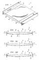
- FIG. 1is a prospective view of an optical device in accordance with the present invention
- FIG. 2is a vertical sectional view of an optical device and system in accordance with the present invention.
- FIG. 3Ais a vertical sectional view of alternative embodiment of an optical device and system in accordance with the present invention.
- FIG. 3Bis a vertical sectional view of yet alternative embodiment of an optical device and system in accordance with the present invention.
- FIG. 4is a vertical sectional view of yet another embodiment of an optical device and system in accordance with the present invention.
- FIG. 5is a vertical sectional view of still another embodiment of an optical device and system in accordance with the present invention.
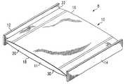
- FIG. 6is a perspective view of a digital film processing system in accordance with the present invention.
- FIGS. 1 and 2illustrate an optical transfer system 8 in accordance with one embodiment of the invention.
- the optical transfer system 8comprises a light source 12 and a waveguide device 10 .
- the light source 12 and waveguide device 10 of the optical transfer system 8can be assembled using fixtures and techniques known in the industry.
- the present inventioncan be used in a variety of suitable articles and devices desiring the collection and transfer of light, such as a digital film processing system (see FIG. 6 ), a copier, a scanner, and various medical devices.
- Light source 12 in the optical transfer system 8is generally positioned relative to the waveguide device 10 so that the transfer or transmission of light to the waveguide device 10 is optimized.
- the light source 12is positioned adjacent one end 22 of the waveguide device 10 , and preferably, in an abutting relationship with end 22 , as exemplified in FIG. 2 .
- Examples of light source 12 used with the present inventioncan include a source of electromagnetic radiation, a laser, an LED light array, fluorescent light tubes, or any other suitable light source.
- Waveguide device 10assists in the transfer or transmission of light over an extended distance and/or to hard to reach areas.
- waveguide device 10includes a generally longitudinally extending solid body 11 for transmitting light.
- the body 11has a longitudinal axis L and a transverse axis T generally along the waveguide device's centerline, which is preferably generally perpendicular to the longitudinal axis L.
- the waveguide device 10comprises a generally elliptical shaped vertical cross sectional configuration along its longitudinal axis L, as exemplified in FIGS. 2-5.
- Waveguide device 10includes a first surface 16 , and a second surface 18 , which generally define two outer boundaries of the waveguide device 10 , and/or interfaces with the surrounding material, which can be air.
- First surface 16 and/or second surface 18are preferably oriented in a non-parallel relationship to the longitudinal axis L, and ⁇ or to each other.
- the waveguide device 10can have a generally overall elliptical cross sectional shaped configuration.
- the orientation of first surface 16 and a second surface 18respectively, can be selected to enhance and/or maximize the collection angle of the waveguide device 10 , preferably so that it can approach about 180 degrees relative to the longitudinal axis L, and maintain total internal reflection.
- proximal portion 20 of the waveguide device 10is provided, generally adjacent the light source 12
- distal portion 30 of the waveguide device 10is generally provided adjacent the image plane 14 .
- Body 11 of the waveguide device 10can be made from any material that will transfer or transmit light.
- materials which are suitable for body 11can include dielectric materials, glass and plastics, such as acrylics, polystyrenes, polycarbonates, and other dielectric materials that transmit light.
- the materialmay also include additives to enhance the durability, the strength of the material, the optical quality, the heat resistance, and the flame retardants of the body 11 .
- the material of body 11will be homogeneous to assist in reducing light scattering.
- the material of body 11is non-homogeneous and includes materials of varying densities to focus the light.
- the densities of non-homogeneous material of body 11can vary in the form of a gradient that decreases in density, preferably linearly decreases, from the longitudinal axis L outwardly along the transverse axis T toward the first surface 16 and second surface 18 .
- Body 11also preferably will be resistant to scratching so that the waveguide device 10 is durable and wear resistant.
- Materials used for body 11will have a suitable index of refraction to enhance light retention in the waveguide device 10 , and to minimize the loss of light due to light refraction.
- the index of refraction of body 11is greater than or equal to about 1.4, more preferably from about 1.4 to about 1.6, and most preferably about 1.5.
- the body 11may include a coating 19 to enhance wear resistance and durability, and/or to assist in preserving total internal reflection.
- coating 19include materials and coating that are used with eyeglass lens, or contact lenses.
- image plane 14can be positioned so that light can be transmitted or transferred from waveguide device 10 to the image plane 14 , and preferably, so that the irradiation of the light on the image plane 14 is enhanced.
- the image plane 14can be positioned or provided adjacent an oppositively disposed end 34 of the waveguide device 10 .
- Image plane 14can include various media and articles, including but not limited to, photographic media, paper, film, photodiodes, any media illuminator, and other medias and articles that will display a light image.
- distal portion 30may include an end surface 32 , which is generally configured to sharped the focus of the light on the image plane 14 .
- the length between end surface 32 and image plane 14operates to vary the focus point of the light being emitted from the waveguide device 10 .
- the length between end surface 32 and image plane 14can vary depending on whether it is desirable to reduce the loss of light, or to enhance the focus of the light on the image plane 14 .
- the longer the length between end surface 32 and image plane 14the further the focus point of the light is away from the image plane 14 .
- the end surface 32may be configured in a parallel orientation relative to transverse axis T. In another embodiment, the end surface 32 may be configured in a hyperbolic or spherical surface, in an aspherical surface (e.g., see FIG. 3 B), or in another shape to assist in compensating for the air/material interface refraction. In certain applications, the waveguide device 10 may be manufactured with end surface 32 . Alternatively, an end portion 34 may be removed after manufacturing whereby the waveguide device 10 could be tailored to a particular need or situation.
- waveguide device 10includes a hollow chamber 17 between the first surface 16 and the second surface 18 that is filled with material more transmissive, more homogeneous, and/or having a lower refractive index than body 11 , such as air.
- coating 19such as a reflective coating, may be used to assist in enhancing the focus point of the light on the image plane 14 , and to minimizing or eliminate refraction of the light out of the waveguide device 10 .
- the coating 19may be applied to either the inner surface 16 A of the first surface 16 , and/or the inner surface 18 A of the second surface 18 (See e.g., FIG.
- the coating 19is clear. Selection and placement of the coating 19 operates to optimize the transfer of light depending on the wavelength of light being transmitted through the waveguide device 10 . For example, a coating 19 of a bare gold is preferred for use with near infrared light, whereas a coating 19 of silver and aluminum may be preferred for use with visible light.
- a digital film processing system 100operates by converting electromagnetic radiation from an image to an electronic (digital) representation of the image.
- the image being scannedis typically embodied in a physical form or an image plane (e.g., 14 ), such as on a photographic media or film 112 , although other media may be used.
- the electromagnetic radiation used to convert the image into a digitized representationis preferably infrared light.
- the digital film processing system 100generally includes at least one and preferably a number of optic sensors 102 .
- the optic sensors 102detect light and measure the intensity of electromagnetic energy passing through or reflected by the film 112 .
- the source of electromagnetic energyis typically a light source 12 , which illuminates the film 112 containing the scene image 104 . Radiation from the light source 12 may be diffused or directed by additional optics such as filters (not shown) and one or more lens 106 . Waveguide device 10 is positioned between the light source 12 and the film 112 to direct light to the film 112 , and in order to illuminate the images 104 and 108 more uniformly.
- Light source 12is positioned on the side of the film 112 opposite the optic sensors 102 . This placement results in sensors 102 detecting radiation emitted from light source 12 as it passes through the images 104 and 108 on the film 112 .
- Another light source 111is shown placed on the same side of the film 112 as the sensors 102 . When light source 111 is activated, sensors 102 detect radiation reflected by the images 104 and 108 .
Landscapes
- Physics & Mathematics (AREA)
- Optics & Photonics (AREA)
- General Physics & Mathematics (AREA)
- Engineering & Computer Science (AREA)
- Multimedia (AREA)
- Signal Processing (AREA)
- Optical Couplings Of Light Guides (AREA)
Abstract
Description
Claims (6)
Priority Applications (2)
| Application Number | Priority Date | Filing Date | Title |
|---|---|---|---|
| US09/730,332US6628884B2 (en) | 1999-12-30 | 2000-12-05 | Digital film processing system using a light transfer device |
| US10/660,214US6888997B2 (en) | 2000-12-05 | 2003-09-11 | Waveguide device and optical transfer system for directing light to an image plane |
Applications Claiming Priority (2)
| Application Number | Priority Date | Filing Date | Title |
|---|---|---|---|
| US17378399P | 1999-12-30 | 1999-12-30 | |
| US09/730,332US6628884B2 (en) | 1999-12-30 | 2000-12-05 | Digital film processing system using a light transfer device |
Related Child Applications (1)
| Application Number | Title | Priority Date | Filing Date |
|---|---|---|---|
| US10/660,214DivisionUS6888997B2 (en) | 2000-12-05 | 2003-09-11 | Waveguide device and optical transfer system for directing light to an image plane |
Publications (2)
| Publication Number | Publication Date |
|---|---|
| US20010031125A1 US20010031125A1 (en) | 2001-10-18 |
| US6628884B2true US6628884B2 (en) | 2003-09-30 |
Family
ID=26869528
Family Applications (1)
| Application Number | Title | Priority Date | Filing Date |
|---|---|---|---|
| US09/730,332Expired - Fee RelatedUS6628884B2 (en) | 1999-12-30 | 2000-12-05 | Digital film processing system using a light transfer device |
Country Status (1)
| Country | Link |
|---|---|
| US (1) | US6628884B2 (en) |
Cited By (1)
| Publication number | Priority date | Publication date | Assignee | Title |
|---|---|---|---|---|
| US20050023449A1 (en)* | 2003-07-31 | 2005-02-03 | Gruhlke Russell W. | Method and apparatus for improved collection efficiency of speckle based navigation sensors using lightpipes and reflectors |
Citations (34)
| Publication number | Priority date | Publication date | Assignee | Title |
|---|---|---|---|---|
| US3771077A (en)* | 1970-09-24 | 1973-11-06 | F Tischer | Waveguide and circuit using the waveguide to interconnect the parts |
| US3790905A (en)* | 1970-12-03 | 1974-02-05 | Licentia Gmbh | Waveguide for simultaneously transmitting two electromagnetic waves |
| US3833161A (en) | 1972-02-08 | 1974-09-03 | Bosch Photokino Gmbh | Apparatus for intercepting and threading the leader of convoluted motion picture film or the like |
| US4265545A (en) | 1979-07-27 | 1981-05-05 | Intec Corporation | Multiple source laser scanning inspection system |
| US4633300A (en) | 1983-10-21 | 1986-12-30 | Canon Kabushiki Kaisha | Color information detecting device |
| US4741621A (en) | 1986-08-18 | 1988-05-03 | Westinghouse Electric Corp. | Geometric surface inspection system with dual overlap light stripe generator |
| US5027146A (en) | 1989-08-31 | 1991-06-25 | Eastman Kodak Company | Processing apparatus |
| US5200817A (en) | 1991-08-29 | 1993-04-06 | Xerox Corporation | Conversion of an RGB color scanner into a colorimetric scanner |
| EP0580293A1 (en) | 1992-07-17 | 1994-01-26 | International Business Machines Corporation | Scanning film during the film process |
| EP0601364A1 (en) | 1992-11-30 | 1994-06-15 | Konica Corporation | Film image editing apparatus |
| US5334247A (en) | 1991-07-25 | 1994-08-02 | Eastman Kodak Company | Coater design for low flowrate coating applications |
| US5477345A (en) | 1993-12-15 | 1995-12-19 | Xerox Corporation | Apparatus for subsampling chrominance |
| US5587752A (en) | 1995-06-05 | 1996-12-24 | Eastman Kodak Company | Camera, system and method for producing composite photographic image |
| EP0768571A2 (en) | 1995-09-18 | 1997-04-16 | Noritsu Koki Co., Ltd. | Film connecting device |
| US5627016A (en) | 1996-02-29 | 1997-05-06 | Eastman Kodak Company | Method and apparatus for photofinishing photosensitive film |
| US5644356A (en)* | 1994-02-01 | 1997-07-01 | Rank Cintel Limited | High resolution film scanner |
| US5649260A (en) | 1995-06-26 | 1997-07-15 | Eastman Kodak Company | Automated photofinishing apparatus |
| EP0806861A1 (en) | 1996-05-10 | 1997-11-12 | Noritsu Koki Co., Ltd. | Electronic image printing apparatus attachable to a photographic processing apparatus |
| WO1998025399A1 (en) | 1996-12-05 | 1998-06-11 | Applied Science Fiction, Inc. | Method and apparatus for reducing noise in electronic film development |
| WO1998034157A2 (en) | 1997-01-30 | 1998-08-06 | Applied Science Fiction, Inc. | System and method for latent film recovery in electronic film development |
| US5835795A (en) | 1996-06-25 | 1998-11-10 | Photo Dimensions | Blended photographic composite images |
| EP0878777A2 (en) | 1997-05-09 | 1998-11-18 | Xerox Corporation | Method for enhancement of reduced color set images |
| WO1999043149A1 (en) | 1998-02-23 | 1999-08-26 | Applied Science Fiction, Inc. | Progressive area scan in electronic film development |
| US5952665A (en)* | 1997-11-28 | 1999-09-14 | Nanocrystals Technology L.P. | Composite nanophosphor screen for detecting radiation |
| US5959720A (en) | 1996-03-22 | 1999-09-28 | Eastman Kodak Company | Method for color balance determination |
| JP2000068732A (en)* | 1998-08-26 | 2000-03-03 | Hitachi Cable Ltd | Leaky waveguide |
| US6088084A (en) | 1997-10-17 | 2000-07-11 | Fuji Photo Film Co., Ltd. | Original carrier and image reader |
| US6200738B1 (en)* | 1998-10-29 | 2001-03-13 | Konica Corporation | Image forming method |
| WO2001045042A1 (en) | 1999-12-17 | 2001-06-21 | Applied Science Fiction, Inc. | Method and system for selective enhancement of image data |
| WO2001050194A1 (en) | 1999-12-30 | 2001-07-12 | Applied Science Fiction, Inc. | System and method for digital film development using visible light |
| WO2001050197A1 (en) | 1999-12-30 | 2001-07-12 | Applied Science Fiction, Inc. | System and method for digital color dye film processing |
| WO2001050192A1 (en) | 1999-12-31 | 2001-07-12 | Applied Science Fiction, Inc. | Digital film processing method |
| WO2001050193A1 (en) | 1999-12-30 | 2001-07-12 | Applied Science Fiction, Inc. | Improved system and method for digital film development using visible light |
| WO2001052556A2 (en) | 1999-12-30 | 2001-07-19 | Applied Science Fiction, Inc. | Methods and apparatus for transporting and positioning film in a digital film processing system |
- 2000
- 2000-12-05USUS09/730,332patent/US6628884B2/ennot_activeExpired - Fee Related
Patent Citations (34)
| Publication number | Priority date | Publication date | Assignee | Title |
|---|---|---|---|---|
| US3771077A (en)* | 1970-09-24 | 1973-11-06 | F Tischer | Waveguide and circuit using the waveguide to interconnect the parts |
| US3790905A (en)* | 1970-12-03 | 1974-02-05 | Licentia Gmbh | Waveguide for simultaneously transmitting two electromagnetic waves |
| US3833161A (en) | 1972-02-08 | 1974-09-03 | Bosch Photokino Gmbh | Apparatus for intercepting and threading the leader of convoluted motion picture film or the like |
| US4265545A (en) | 1979-07-27 | 1981-05-05 | Intec Corporation | Multiple source laser scanning inspection system |
| US4633300A (en) | 1983-10-21 | 1986-12-30 | Canon Kabushiki Kaisha | Color information detecting device |
| US4741621A (en) | 1986-08-18 | 1988-05-03 | Westinghouse Electric Corp. | Geometric surface inspection system with dual overlap light stripe generator |
| US5027146A (en) | 1989-08-31 | 1991-06-25 | Eastman Kodak Company | Processing apparatus |
| US5334247A (en) | 1991-07-25 | 1994-08-02 | Eastman Kodak Company | Coater design for low flowrate coating applications |
| US5200817A (en) | 1991-08-29 | 1993-04-06 | Xerox Corporation | Conversion of an RGB color scanner into a colorimetric scanner |
| EP0580293A1 (en) | 1992-07-17 | 1994-01-26 | International Business Machines Corporation | Scanning film during the film process |
| EP0601364A1 (en) | 1992-11-30 | 1994-06-15 | Konica Corporation | Film image editing apparatus |
| US5477345A (en) | 1993-12-15 | 1995-12-19 | Xerox Corporation | Apparatus for subsampling chrominance |
| US5644356A (en)* | 1994-02-01 | 1997-07-01 | Rank Cintel Limited | High resolution film scanner |
| US5587752A (en) | 1995-06-05 | 1996-12-24 | Eastman Kodak Company | Camera, system and method for producing composite photographic image |
| US5649260A (en) | 1995-06-26 | 1997-07-15 | Eastman Kodak Company | Automated photofinishing apparatus |
| EP0768571A2 (en) | 1995-09-18 | 1997-04-16 | Noritsu Koki Co., Ltd. | Film connecting device |
| US5627016A (en) | 1996-02-29 | 1997-05-06 | Eastman Kodak Company | Method and apparatus for photofinishing photosensitive film |
| US5959720A (en) | 1996-03-22 | 1999-09-28 | Eastman Kodak Company | Method for color balance determination |
| EP0806861A1 (en) | 1996-05-10 | 1997-11-12 | Noritsu Koki Co., Ltd. | Electronic image printing apparatus attachable to a photographic processing apparatus |
| US5835795A (en) | 1996-06-25 | 1998-11-10 | Photo Dimensions | Blended photographic composite images |
| WO1998025399A1 (en) | 1996-12-05 | 1998-06-11 | Applied Science Fiction, Inc. | Method and apparatus for reducing noise in electronic film development |
| WO1998034157A2 (en) | 1997-01-30 | 1998-08-06 | Applied Science Fiction, Inc. | System and method for latent film recovery in electronic film development |
| EP0878777A2 (en) | 1997-05-09 | 1998-11-18 | Xerox Corporation | Method for enhancement of reduced color set images |
| US6088084A (en) | 1997-10-17 | 2000-07-11 | Fuji Photo Film Co., Ltd. | Original carrier and image reader |
| US5952665A (en)* | 1997-11-28 | 1999-09-14 | Nanocrystals Technology L.P. | Composite nanophosphor screen for detecting radiation |
| WO1999043149A1 (en) | 1998-02-23 | 1999-08-26 | Applied Science Fiction, Inc. | Progressive area scan in electronic film development |
| JP2000068732A (en)* | 1998-08-26 | 2000-03-03 | Hitachi Cable Ltd | Leaky waveguide |
| US6200738B1 (en)* | 1998-10-29 | 2001-03-13 | Konica Corporation | Image forming method |
| WO2001045042A1 (en) | 1999-12-17 | 2001-06-21 | Applied Science Fiction, Inc. | Method and system for selective enhancement of image data |
| WO2001050194A1 (en) | 1999-12-30 | 2001-07-12 | Applied Science Fiction, Inc. | System and method for digital film development using visible light |
| WO2001050197A1 (en) | 1999-12-30 | 2001-07-12 | Applied Science Fiction, Inc. | System and method for digital color dye film processing |
| WO2001050193A1 (en) | 1999-12-30 | 2001-07-12 | Applied Science Fiction, Inc. | Improved system and method for digital film development using visible light |
| WO2001052556A2 (en) | 1999-12-30 | 2001-07-19 | Applied Science Fiction, Inc. | Methods and apparatus for transporting and positioning film in a digital film processing system |
| WO2001050192A1 (en) | 1999-12-31 | 2001-07-12 | Applied Science Fiction, Inc. | Digital film processing method |
Cited By (2)
| Publication number | Priority date | Publication date | Assignee | Title |
|---|---|---|---|---|
| US20050023449A1 (en)* | 2003-07-31 | 2005-02-03 | Gruhlke Russell W. | Method and apparatus for improved collection efficiency of speckle based navigation sensors using lightpipes and reflectors |
| US7041964B2 (en)* | 2003-07-31 | 2006-05-09 | Avago Technology, Ltd. | Method and apparatus for improved collection efficiency of speckle based navigation sensors using lightpipes and reflectors |
Also Published As
| Publication number | Publication date |
|---|---|
| US20010031125A1 (en) | 2001-10-18 |
Similar Documents
| Publication | Publication Date | Title |
|---|---|---|
| KR0155034B1 (en) | Uneven surface reader | |
| US6429927B1 (en) | Imaging device, especially for optical fingerprinting | |
| US7315632B2 (en) | Device for imaging the papillary lines of a finger | |
| US5416608A (en) | Image reading apparatus | |
| US6888997B2 (en) | Waveguide device and optical transfer system for directing light to an image plane | |
| US20230028172A1 (en) | Device for optical imaging of features of a hand | |
| JP2018200468A (en) | Optical system for light collection | |
| KR101738188B1 (en) | Relief pattern detection device | |
| JPH0560538A (en) | Optical measurement machine | |
| JP2592192B2 (en) | Irradiation device for document scanning device | |
| KR20060023571A (en) | Light guide and image reading device | |
| US5256868A (en) | Contact scanners for scanning images of an illuminated film onto a photosensor array | |
| US6628884B2 (en) | Digital film processing system using a light transfer device | |
| US4907026A (en) | Light projection system for automatic focus detection | |
| JP2005503702A (en) | Optical system, optical element, and user unit for illuminating a subject for imaging | |
| JP3110745B2 (en) | Optical document scanning device | |
| PL1683073T3 (en) | Optical imaging device suited for forming an image of fingerprints | |
| US5526458A (en) | Vision system with fiber optic plate to detilt oblique images | |
| JP2003524956A (en) | Document reading device having waveguide formed on substrate | |
| JPH09257696A (en) | Surface plasmon resonance sensor | |
| JP3662125B2 (en) | Lighting device | |
| CN107402439B (en) | Thin plate imaging device | |
| JPH10257247A (en) | Image reader and scanner | |
| JPH08211268A (en) | Optical refractive-index matching system | |
| MXPA00012484A (en) | Apparatus and method for detecting the level of a liquid |
Legal Events
| Date | Code | Title | Description |
|---|---|---|---|
| AS | Assignment | Owner name:APPLIED SCIENCE FICTION, INC., TEXAS Free format text:ASSIGNMENT OF ASSIGNORS INTEREST;ASSIGNOR:DUONG, DUNG T.;REEL/FRAME:011721/0846 Effective date:20000713 | |
| AS | Assignment | Owner name:CENTERPOINT VENTURE PARTNERS, L.P., TEXAS Free format text:SECURITY AGREEMENT;ASSIGNOR:APPLIED SCIENCE FICTION, INC.;REEL/FRAME:012997/0211 Effective date:20020723 Owner name:CENTERPOINT VENTURE PARTNERS, L.P., TEXAS Free format text:SECURITY INTEREST;ASSIGNOR:APPLIED SCIENCE FICTION, INC.;REEL/FRAME:012997/0113 Effective date:20020723 Owner name:RHO VENTURES (QP), L.P., NEW YORK Free format text:SECURITY AGREEMENT;ASSIGNOR:APPLIED SCIENCE FICTION, INC.;REEL/FRAME:012997/0211 Effective date:20020723 Owner name:RHO VENTURES (QP), L.P., NEW YORK Free format text:SECURITY INTEREST;ASSIGNOR:APPLIED SCIENCE FICTION, INC.;REEL/FRAME:012997/0113 Effective date:20020723 | |
| AS | Assignment | Owner name:CENTERPOINT VENTURE PARTNERS, L.P., TEXAS Free format text:SECURITY AGREEMENT;ASSIGNOR:APPLIED SCIENCE FICTION, INC.;REEL/FRAME:013506/0065 Effective date:20030213 Owner name:RHO VENTURES (QP), L.P., NEW YORK Free format text:SECURITY AGREEMENT;ASSIGNOR:APPLIED SCIENCE FICTION, INC.;REEL/FRAME:013506/0065 Effective date:20030213 | |
| AS | Assignment | Owner name:EASTMAN KODAK COMPANY, NEW YORK Free format text:ASSIGNMENT OF ASSIGNORS INTEREST;ASSIGNOR:APPLIED SCIENCE FICTION, INC.;REEL/FRAME:014293/0774 Effective date:20030521 | |
| FEPP | Fee payment procedure | Free format text:PAYOR NUMBER ASSIGNED (ORIGINAL EVENT CODE: ASPN); ENTITY STATUS OF PATENT OWNER: LARGE ENTITY | |
| FPAY | Fee payment | Year of fee payment:4 | |
| FPAY | Fee payment | Year of fee payment:8 | |
| AS | Assignment | Owner name:EASTMAN KODAK COMPANY, NEW YORK Free format text:RELEASE BY SECURED PARTY;ASSIGNORS:CENTERPOINT VENTURE PARTNERS, L.P.;RHO VENTURES (QP), L.P.;REEL/FRAME:027294/0740 Effective date:20030521 Owner name:APPLIED SCIENCE FICTION, INC., TEXAS Free format text:RELEASE BY SECURED PARTY;ASSIGNORS:CENTERPOINT VENTURE PARTNERS, L.P.;RHO VENTURES (QP), L.P.;REEL/FRAME:027294/0740 Effective date:20030521 | |
| AS | Assignment | Owner name:CITICORP NORTH AMERICA, INC., AS AGENT, NEW YORK Free format text:SECURITY INTEREST;ASSIGNORS:EASTMAN KODAK COMPANY;PAKON, INC.;REEL/FRAME:028201/0420 Effective date:20120215 | |
| AS | Assignment | Owner name:WILMINGTON TRUST, NATIONAL ASSOCIATION, AS AGENT, Free format text:PATENT SECURITY AGREEMENT;ASSIGNORS:EASTMAN KODAK COMPANY;PAKON, INC.;REEL/FRAME:030122/0235 Effective date:20130322 Owner name:WILMINGTON TRUST, NATIONAL ASSOCIATION, AS AGENT, MINNESOTA Free format text:PATENT SECURITY AGREEMENT;ASSIGNORS:EASTMAN KODAK COMPANY;PAKON, INC.;REEL/FRAME:030122/0235 Effective date:20130322 | |
| AS | Assignment | Owner name:BANK OF AMERICA N.A., AS AGENT, MASSACHUSETTS Free format text:INTELLECTUAL PROPERTY SECURITY AGREEMENT (ABL);ASSIGNORS:EASTMAN KODAK COMPANY;FAR EAST DEVELOPMENT LTD.;FPC INC.;AND OTHERS;REEL/FRAME:031162/0117 Effective date:20130903 Owner name:BARCLAYS BANK PLC, AS ADMINISTRATIVE AGENT, NEW YORK Free format text:INTELLECTUAL PROPERTY SECURITY AGREEMENT (SECOND LIEN);ASSIGNORS:EASTMAN KODAK COMPANY;FAR EAST DEVELOPMENT LTD.;FPC INC.;AND OTHERS;REEL/FRAME:031159/0001 Effective date:20130903 Owner name:JPMORGAN CHASE BANK, N.A., AS ADMINISTRATIVE, DELAWARE Free format text:INTELLECTUAL PROPERTY SECURITY AGREEMENT (FIRST LIEN);ASSIGNORS:EASTMAN KODAK COMPANY;FAR EAST DEVELOPMENT LTD.;FPC INC.;AND OTHERS;REEL/FRAME:031158/0001 Effective date:20130903 Owner name:BARCLAYS BANK PLC, AS ADMINISTRATIVE AGENT, NEW YO Free format text:INTELLECTUAL PROPERTY SECURITY AGREEMENT (SECOND LIEN);ASSIGNORS:EASTMAN KODAK COMPANY;FAR EAST DEVELOPMENT LTD.;FPC INC.;AND OTHERS;REEL/FRAME:031159/0001 Effective date:20130903 Owner name:PAKON, INC., NEW YORK Free format text:RELEASE OF SECURITY INTEREST IN PATENTS;ASSIGNORS:CITICORP NORTH AMERICA, INC., AS SENIOR DIP AGENT;WILMINGTON TRUST, NATIONAL ASSOCIATION, AS JUNIOR DIP AGENT;REEL/FRAME:031157/0451 Effective date:20130903 Owner name:JPMORGAN CHASE BANK, N.A., AS ADMINISTRATIVE, DELA Free format text:INTELLECTUAL PROPERTY SECURITY AGREEMENT (FIRST LIEN);ASSIGNORS:EASTMAN KODAK COMPANY;FAR EAST DEVELOPMENT LTD.;FPC INC.;AND OTHERS;REEL/FRAME:031158/0001 Effective date:20130903 Owner name:EASTMAN KODAK COMPANY, NEW YORK Free format text:RELEASE OF SECURITY INTEREST IN PATENTS;ASSIGNORS:CITICORP NORTH AMERICA, INC., AS SENIOR DIP AGENT;WILMINGTON TRUST, NATIONAL ASSOCIATION, AS JUNIOR DIP AGENT;REEL/FRAME:031157/0451 Effective date:20130903 | |
| REMI | Maintenance fee reminder mailed | ||
| LAPS | Lapse for failure to pay maintenance fees | ||
| STCH | Information on status: patent discontinuation | Free format text:PATENT EXPIRED DUE TO NONPAYMENT OF MAINTENANCE FEES UNDER 37 CFR 1.362 | |
| FP | Lapsed due to failure to pay maintenance fee | Effective date:20150930 | |
| AS | Assignment | Owner name:PAKON, INC., NEW YORK Free format text:RELEASE BY SECURED PARTY;ASSIGNOR:JP MORGAN CHASE BANK, N.A., AS ADMINISTRATIVE AGENT;REEL/FRAME:049814/0001 Effective date:20190617 Owner name:FAR EAST DEVELOPMENT LTD., NEW YORK Free format text:RELEASE BY SECURED PARTY;ASSIGNOR:JP MORGAN CHASE BANK, N.A., AS ADMINISTRATIVE AGENT;REEL/FRAME:049814/0001 Effective date:20190617 Owner name:KODAK IMAGING NETWORK, INC., NEW YORK Free format text:RELEASE BY SECURED PARTY;ASSIGNOR:JP MORGAN CHASE BANK, N.A., AS ADMINISTRATIVE AGENT;REEL/FRAME:049814/0001 Effective date:20190617 Owner name:LASER PACIFIC MEDIA CORPORATION, NEW YORK Free format text:RELEASE BY SECURED PARTY;ASSIGNOR:JP MORGAN CHASE BANK, N.A., AS ADMINISTRATIVE AGENT;REEL/FRAME:049814/0001 Effective date:20190617 Owner name:KODAK PORTUGUESA LIMITED, NEW YORK Free format text:RELEASE BY SECURED PARTY;ASSIGNOR:JP MORGAN CHASE BANK, N.A., AS ADMINISTRATIVE AGENT;REEL/FRAME:049814/0001 Effective date:20190617 Owner name:KODAK PHILIPPINES, LTD., NEW YORK Free format text:RELEASE BY SECURED PARTY;ASSIGNOR:JP MORGAN CHASE BANK, N.A., AS ADMINISTRATIVE AGENT;REEL/FRAME:049814/0001 Effective date:20190617 Owner name:KODAK (NEAR EAST), INC., NEW YORK Free format text:RELEASE BY SECURED PARTY;ASSIGNOR:JP MORGAN CHASE BANK, N.A., AS ADMINISTRATIVE AGENT;REEL/FRAME:049814/0001 Effective date:20190617 Owner name:KODAK REALTY, INC., NEW YORK Free format text:RELEASE BY SECURED PARTY;ASSIGNOR:JP MORGAN CHASE BANK, N.A., AS ADMINISTRATIVE AGENT;REEL/FRAME:049814/0001 Effective date:20190617 Owner name:NPEC, INC., NEW YORK Free format text:RELEASE BY SECURED PARTY;ASSIGNOR:JP MORGAN CHASE BANK, N.A., AS ADMINISTRATIVE AGENT;REEL/FRAME:049814/0001 Effective date:20190617 Owner name:EASTMAN KODAK COMPANY, NEW YORK Free format text:RELEASE BY SECURED PARTY;ASSIGNOR:JP MORGAN CHASE BANK, N.A., AS ADMINISTRATIVE AGENT;REEL/FRAME:049814/0001 Effective date:20190617 Owner name:KODAK AVIATION LEASING LLC, NEW YORK Free format text:RELEASE BY SECURED PARTY;ASSIGNOR:JP MORGAN CHASE BANK, N.A., AS ADMINISTRATIVE AGENT;REEL/FRAME:049814/0001 Effective date:20190617 Owner name:CREO MANUFACTURING AMERICA LLC, NEW YORK Free format text:RELEASE BY SECURED PARTY;ASSIGNOR:JP MORGAN CHASE BANK, N.A., AS ADMINISTRATIVE AGENT;REEL/FRAME:049814/0001 Effective date:20190617 Owner name:FPC, INC., NEW YORK Free format text:RELEASE BY SECURED PARTY;ASSIGNOR:JP MORGAN CHASE BANK, N.A., AS ADMINISTRATIVE AGENT;REEL/FRAME:049814/0001 Effective date:20190617 Owner name:QUALEX, INC., NEW YORK Free format text:RELEASE BY SECURED PARTY;ASSIGNOR:JP MORGAN CHASE BANK, N.A., AS ADMINISTRATIVE AGENT;REEL/FRAME:049814/0001 Effective date:20190617 Owner name:KODAK AMERICAS, LTD., NEW YORK Free format text:RELEASE BY SECURED PARTY;ASSIGNOR:JP MORGAN CHASE BANK, N.A., AS ADMINISTRATIVE AGENT;REEL/FRAME:049814/0001 Effective date:20190617 | |
| AS | Assignment | Owner name:FPC INC., NEW YORK Free format text:RELEASE BY SECURED PARTY;ASSIGNOR:BARCLAYS BANK PLC;REEL/FRAME:052773/0001 Effective date:20170202 Owner name:NPEC INC., NEW YORK Free format text:RELEASE BY SECURED PARTY;ASSIGNOR:BARCLAYS BANK PLC;REEL/FRAME:052773/0001 Effective date:20170202 Owner name:FAR EAST DEVELOPMENT LTD., NEW YORK Free format text:RELEASE BY SECURED PARTY;ASSIGNOR:BARCLAYS BANK PLC;REEL/FRAME:052773/0001 Effective date:20170202 Owner name:KODAK REALTY INC., NEW YORK Free format text:RELEASE BY SECURED PARTY;ASSIGNOR:BARCLAYS BANK PLC;REEL/FRAME:052773/0001 Effective date:20170202 Owner name:EASTMAN KODAK COMPANY, NEW YORK Free format text:RELEASE BY SECURED PARTY;ASSIGNOR:BARCLAYS BANK PLC;REEL/FRAME:052773/0001 Effective date:20170202 Owner name:KODAK AMERICAS LTD., NEW YORK Free format text:RELEASE BY SECURED PARTY;ASSIGNOR:BARCLAYS BANK PLC;REEL/FRAME:052773/0001 Effective date:20170202 Owner name:LASER PACIFIC MEDIA CORPORATION, NEW YORK Free format text:RELEASE BY SECURED PARTY;ASSIGNOR:BARCLAYS BANK PLC;REEL/FRAME:052773/0001 Effective date:20170202 Owner name:QUALEX INC., NEW YORK Free format text:RELEASE BY SECURED PARTY;ASSIGNOR:BARCLAYS BANK PLC;REEL/FRAME:052773/0001 Effective date:20170202 Owner name:KODAK (NEAR EAST) INC., NEW YORK Free format text:RELEASE BY SECURED PARTY;ASSIGNOR:BARCLAYS BANK PLC;REEL/FRAME:052773/0001 Effective date:20170202 Owner name:KODAK PHILIPPINES LTD., NEW YORK Free format text:RELEASE BY SECURED PARTY;ASSIGNOR:BARCLAYS BANK PLC;REEL/FRAME:052773/0001 Effective date:20170202 |