US6628531B2 - Multi-layer and user-configurable micro-printed circuit board - Google Patents
Multi-layer and user-configurable micro-printed circuit boardDownload PDFInfo
- Publication number
- US6628531B2 US6628531B2US09/735,030US73503000AUS6628531B2US 6628531 B2US6628531 B2US 6628531B2US 73503000 AUS73503000 AUS 73503000AUS 6628531 B2US6628531 B2US 6628531B2
- Authority
- US
- United States
- Prior art keywords
- printed circuit
- circuit boards
- circuit board
- pcb
- winding
- Prior art date
- Legal status (The legal status is an assumption and is not a legal conclusion. Google has not performed a legal analysis and makes no representation as to the accuracy of the status listed.)
- Expired - Lifetime
Links
Images


Classifications
- H—ELECTRICITY
- H05—ELECTRIC TECHNIQUES NOT OTHERWISE PROVIDED FOR
- H05K—PRINTED CIRCUITS; CASINGS OR CONSTRUCTIONAL DETAILS OF ELECTRIC APPARATUS; MANUFACTURE OF ASSEMBLAGES OF ELECTRICAL COMPONENTS
- H05K1/00—Printed circuits
- H05K1/16—Printed circuits incorporating printed electric components, e.g. printed resistor, capacitor, inductor
- H05K1/165—Printed circuits incorporating printed electric components, e.g. printed resistor, capacitor, inductor incorporating printed inductors
- H—ELECTRICITY
- H01—ELECTRIC ELEMENTS
- H01F—MAGNETS; INDUCTANCES; TRANSFORMERS; SELECTION OF MATERIALS FOR THEIR MAGNETIC PROPERTIES
- H01F17/00—Fixed inductances of the signal type
- H01F17/0006—Printed inductances
- H01F17/0013—Printed inductances with stacked layers
- H—ELECTRICITY
- H01—ELECTRIC ELEMENTS
- H01F—MAGNETS; INDUCTANCES; TRANSFORMERS; SELECTION OF MATERIALS FOR THEIR MAGNETIC PROPERTIES
- H01F27/00—Details of transformers or inductances, in general
- H01F27/28—Coils; Windings; Conductive connections
- H01F27/2804—Printed windings
- H—ELECTRICITY
- H05—ELECTRIC TECHNIQUES NOT OTHERWISE PROVIDED FOR
- H05K—PRINTED CIRCUITS; CASINGS OR CONSTRUCTIONAL DETAILS OF ELECTRIC APPARATUS; MANUFACTURE OF ASSEMBLAGES OF ELECTRICAL COMPONENTS
- H05K1/00—Printed circuits
- H05K1/02—Details
- H05K1/0286—Programmable, customizable or modifiable circuits
- H05K1/029—Programmable, customizable or modifiable circuits having a programmable lay-out, i.e. adapted for choosing between a few possibilities
- H—ELECTRICITY
- H05—ELECTRIC TECHNIQUES NOT OTHERWISE PROVIDED FOR
- H05K—PRINTED CIRCUITS; CASINGS OR CONSTRUCTIONAL DETAILS OF ELECTRIC APPARATUS; MANUFACTURE OF ASSEMBLAGES OF ELECTRICAL COMPONENTS
- H05K1/00—Printed circuits
- H05K1/02—Details
- H05K1/14—Structural association of two or more printed circuits
- H05K1/141—One or more single auxiliary printed circuits mounted on a main printed circuit, e.g. modules, adapters
- H—ELECTRICITY
- H05—ELECTRIC TECHNIQUES NOT OTHERWISE PROVIDED FOR
- H05K—PRINTED CIRCUITS; CASINGS OR CONSTRUCTIONAL DETAILS OF ELECTRIC APPARATUS; MANUFACTURE OF ASSEMBLAGES OF ELECTRICAL COMPONENTS
- H05K2201/00—Indexing scheme relating to printed circuits covered by H05K1/00
- H05K2201/08—Magnetic details
- H05K2201/083—Magnetic materials
- H05K2201/086—Magnetic materials for inductive purposes, e.g. printed inductor with ferrite core
- H—ELECTRICITY
- H05—ELECTRIC TECHNIQUES NOT OTHERWISE PROVIDED FOR
- H05K—PRINTED CIRCUITS; CASINGS OR CONSTRUCTIONAL DETAILS OF ELECTRIC APPARATUS; MANUFACTURE OF ASSEMBLAGES OF ELECTRICAL COMPONENTS
- H05K2201/00—Indexing scheme relating to printed circuits covered by H05K1/00
- H05K2201/09—Shape and layout
- H05K2201/09009—Substrate related
- H05K2201/09063—Holes or slots in insulating substrate not used for electrical connections
- H—ELECTRICITY
- H05—ELECTRIC TECHNIQUES NOT OTHERWISE PROVIDED FOR
- H05K—PRINTED CIRCUITS; CASINGS OR CONSTRUCTIONAL DETAILS OF ELECTRIC APPARATUS; MANUFACTURE OF ASSEMBLAGES OF ELECTRICAL COMPONENTS
- H05K2201/00—Indexing scheme relating to printed circuits covered by H05K1/00
- H05K2201/10—Details of components or other objects attached to or integrated in a printed circuit board
- H05K2201/10007—Types of components
- H05K2201/10196—Variable component, e.g. variable resistor
- H—ELECTRICITY
- H05—ELECTRIC TECHNIQUES NOT OTHERWISE PROVIDED FOR
- H05K—PRINTED CIRCUITS; CASINGS OR CONSTRUCTIONAL DETAILS OF ELECTRIC APPARATUS; MANUFACTURE OF ASSEMBLAGES OF ELECTRICAL COMPONENTS
- H05K2201/00—Indexing scheme relating to printed circuits covered by H05K1/00
- H05K2201/10—Details of components or other objects attached to or integrated in a printed circuit board
- H05K2201/10227—Other objects, e.g. metallic pieces
- H05K2201/10295—Metallic connector elements partly mounted in a hole of the PCB
- H05K2201/10303—Pin-in-hole mounted pins
- H—ELECTRICITY
- H05—ELECTRIC TECHNIQUES NOT OTHERWISE PROVIDED FOR
- H05K—PRINTED CIRCUITS; CASINGS OR CONSTRUCTIONAL DETAILS OF ELECTRIC APPARATUS; MANUFACTURE OF ASSEMBLAGES OF ELECTRICAL COMPONENTS
- H05K2203/00—Indexing scheme relating to apparatus or processes for manufacturing printed circuits covered by H05K3/00
- H05K2203/17—Post-manufacturing processes
- H05K2203/171—Tuning, e.g. by trimming of printed components or high frequency circuits
- H—ELECTRICITY
- H05—ELECTRIC TECHNIQUES NOT OTHERWISE PROVIDED FOR
- H05K—PRINTED CIRCUITS; CASINGS OR CONSTRUCTIONAL DETAILS OF ELECTRIC APPARATUS; MANUFACTURE OF ASSEMBLAGES OF ELECTRICAL COMPONENTS
- H05K3/00—Apparatus or processes for manufacturing printed circuits
- H05K3/22—Secondary treatment of printed circuits
- H05K3/222—Completing of printed circuits by adding non-printed jumper connections
- H—ELECTRICITY
- H05—ELECTRIC TECHNIQUES NOT OTHERWISE PROVIDED FOR
- H05K—PRINTED CIRCUITS; CASINGS OR CONSTRUCTIONAL DETAILS OF ELECTRIC APPARATUS; MANUFACTURE OF ASSEMBLAGES OF ELECTRICAL COMPONENTS
- H05K3/00—Apparatus or processes for manufacturing printed circuits
- H05K3/46—Manufacturing multilayer circuits
- H05K3/4611—Manufacturing multilayer circuits by laminating two or more circuit boards
Definitions
- the inventionrelates generally to miniature printed circuit boards (PCB) for microelectrical applications. More particularly, the invention relates to multi-layer, user configurable and stackable miniature printed circuit boards for static electromagnetic components such as transformers.
- Transformersare widely known electromagnetic components used in electrical devices and power supply units.
- static magnetic componentssuch as transformers have traditionally been constructed using windings of ordinary conducting wire having a circular cross section.
- the conventional transformercomprises an insulator gap between a primary coil and a secondary coil, and the voltage generated in the secondary coil is determined by the voltage applied to the primary coil multiplied by the winding ratio between the primary coil and the secondary coil.
- Manufacture of these traditional structuresinvolves winding the wire around a core or bobbin structure, a process that often involves considerable amounts of expensive hand labor.
- high power applicationsoften require a magnetic component having a bulky core and large wire sizes for the windings.
- the transformeris often an essential component of an electrical apparatus, it has been historically the most difficult to miniaturize.
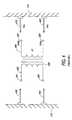
- FIG. 1Aillustrates an example of a typical planar transformer constructed from printed circuit boards. Specifically, FIG. 1A depicts a side view of such a component 100 attached to the main board 110 of an electrical device.
- the component 100includes a PCB 130 with multiple internal layers. Windings of the PCB 130 are connected to the main board by connecting pins 140 .
- FIG. 1Billustrates the manner in which the component 100 is assembled and FIG. 2 schematically depicts the individual layers of the PCB 130 .
- the basic construction of the component 100comprises a spiral conductor on each layer of the PCB 130 forming one or more inductor “turns.”
- the core 120can comprise two separate and identical E-shaped sections 122 and 124 .
- Each E-shaped section 122 , 124includes a middle leg 126 and two outer legs 128 .
- a hole 132is drilled in the center of the PCB 130 .
- the middle leg 126 of the E-shaped section 122 , 124can be supported within the hole 132 to form part of the core 120 .
- the middle leg 126has a circular cross-section and each of the outer legs 128 has a circular or rectangular cross-section.
- the remaining section of the E-shaped sections 122 , 124is formed by a ferrite bar, which is bonded to the legs 126 , 128 .
- the E-shaped sections 122 , 124are assembled so that the legs 126 , 128 of each E-shaped section are bonded together.
- Primary and secondary pins connecting the primary and secondary windings, respectively,can penetrate the PCB via terminal holes 134 drilled near the outer edges of the PCB as will be explained below.
- the width of the spiral conductordepends on the current carrying requirement. That is, the greater the current carrying requirement, the greater the width of the conductor.
- a predetermined areais reserved for the inductor and the one or more turns are printed on each layer according to well known printed circuit board technology. (See, for example, U.S. Pat. No. 5,521,573.) After each layer is so printed, the layers are bonded together into a multi-layer PCB by glass epoxy. Through-hole “vias” or blind “vias” are used to interconnect the turns of the different layers.
- a through-hole viais formed by drilling a hole through the layers at a position to intersect ends of two of the spiral conductors and then “seeding” the inner surface of the holes with a water soluble adhesive. Next, copper is electrolessly plated on the adhesive to interconnect the conductors. Next, additional copper is electrically plated over the electroless copper plate to the desired thickness. Finally, the holes are filled with solder to protect the copper plate.
- a separate viais required for each pair of spiral conductors on adjacent layers to connect all of the turns in series. Each such through-hole via is positioned not to intersect the other conductors.
- Drilling holes in selected layers before the layers are bonded togetherforms a “blind” via. Then, the layers are successively bonded together and, while exposed, the inner surface of the holes is seeded with nickel, electrolessly plated with copper and then filled with solder. The resultant vias extend between the two layers sought to be electrically connected. Thus, the hole does not pass through other layers, and no area is required on these other layers to clear the via.
- the blind via fabrication processis much more expensive than the through-hole fabrication process. As shown in FIG. 1A, primary pins 140 connecting the primary windings and secondary pins 150 connecting the secondary windings are then positioned to penetrate the multi-layer PCB 130 .
- FIG. 2illustrates a process for manufacturing a printed coil with conventional planar technology in a PCB.
- a primary winding and secondary windingcan be formed by connecting multiple coil traces from five layers 200 , 220 , 240 , 260 , and 280 .
- the primary windingfor example, can have an outside terminal 202 connected to a coil trace 204 on layer 200 .
- the inside terminal of the coil trace 204can be connected to an inside terminal of a connection trace 242 on layer 240 by an inner peripheral terminal 208 through a via.
- the outside terminal of the connection trace 242is connected by a primary terminal 210 through a via to an outside terminal 282 of a coil trace 284 on layer 280 .
- the inner terminal of the coil trace 284is connected to the inner terminal of connection trace 244 on layer 240 by a peripheral terminal 286 through a via.
- Connection trace 244is connected to outside terminal 246 , thereby forming a primary winding between outside terminals 202 and 246 from coil traces 204 and 284 on layers 200 and 280 , respectively.
- a secondary windingcan be formed by connecting a coil trace 224 on layer 220 and a coil trace 264 on layer 260 in a similar fashion.
- An outside terminal 262 of coil trace 264can be connected through a via to a corresponding outside terminal 222 of coil trace 224 by a primary terminal 266 .
- the inside terminal of coil trace 224is connected to the inside terminal of coil trace 284 through a via by peripheral terminal 226 . Because the inside terminal of each coil trace 224 and 264 is connected and the outside terminals of each coil trace 224 and 264 is connected, the coil trace 224 and the coil trace 264 are connected in parallel.
- FIG. 3illustrates a typical twelve-layer layout where each individual layer is shown separately. These layers can be connected in a fashion similar to that described above with reference to FIG. 2 to form a PCB having a primary winding and a secondary winding.
- a twelve layer PCBincludes traces of both the primary and secondary windings as similarly described with reference to FIG. 2 .
- the primary and secondary windingsare physically positioned near one another, creating significant risks of electrical flashover.
- FIG. 4schematically illustrates how a primary winding and a secondary winding from a PCB can be arranged as a transformer.
- the windings traced on the layers of a PCBcan form a primary winding with external terminals 202 and 282 and a secondary winding with external terminals 226 and 262 .
- a primary winding 420can be connected to the main board 110 by pins 430 and 440 at terminals 202 and 282 .
- a secondary winding 460can be connected to the main board 110 by pins 470 and 480 at terminals 226 and 262 .
- the primary winding 420is configured across from the secondary winding 460 with the dielectric material of the core 120 positioned therebetween and represented by lines 490 .
- the conventional twelve-layer planar componentsalso prove to be extremely costly.
- the conventional planar magnetic componentmust be customized for each circuit design depending on the parameters required (e.g., the turn ratio). If the parameters change, then a new planar magnetic component must be custom manufactured. Manufacture of the magnetic components using conventional planar technology therefore requires substantial costs associated with each new PCB configuration built for each and every circuit parameter change.
- the current planar technologyraises serious operational problems associated with high potential (HIPOT) applications as well.
- the pins in the conventional boardspenetrate the PCB layers in various locations and generally propagate through the thickness of most or all of the layers; however, only certain pins are electrically bonded to certain layers. Because of the manner in which the pins in the conventional planar components fully penetrate the boards in various locations, with only certain pins electrically bonded to certain layers, significant risks of failure due to an electrical flashover exist.
- such many layer boardsrequire significant pressure to laminate them together, thereby generally creating higher shear forces on the layers during manufacture. The resulting lateral movement of each individual layer relative to the layers above and below can cause significant defects to the operation of the component and, in particular, can infringe the minimum space needed between primary and secondary windings.
- the inventiongenerally comprises a series of discrete stackable PCBs having predetermined trace layouts, such as those used for a cylindrical transformer core. These predetermined boards can be standardized, thereby eliminating the designer layout process.
- the usermay configure the boards using variable position vias (pins) and jumpers such that the vias do not penetrate boards to which they are not electrically connected.
- One embodiment of the inventioncomprises a plurality of core members and a plurality of printed circuit boards stacked into a multi-layer configuration between the core members.
- a first printed circuit boardis configured to define a primary winding of a transformer.
- a second set of printed circuit boardsis configured to define a secondary winding of a transformer.
- a connection memberis configured to selectively connect the printed circuit boards of the secondary winding in either a parallel or a series electrical configuration depending on the needs of the user.
- Connector pinsare configured to electrically connect the plurality of printed circuit boards to the main circuit board. Each connector pin penetrates only printed circuit boards containing the primary winding or the printed circuit boards containing the secondary winding.
- the inventioncomprises a method of manufacturing an electrical device including printing at least one coil on each of a plurality of printed circuit boards, configuring electrical connections on the plurality of printed circuit boards to include the coils on the printed circuit boards so as to define a primary winding and a secondary winding.
- the printed circuit boardsare configured in a stacked arrangement, and the primary winding on the printed circuit boards and the secondary winding on the printed circuit boards are connected to a main circuit board with connector pins in such a manner that the connector pins connecting the primary winding only penetrate printed circuit boards containing the primary winding and connector pins connecting the secondary winding only penetrate printed circuit boards containing the secondary winding.
- FIG. 1Ais a side sectional view of a magnetic component employing the conventional planar technology.
- FIG. 1Bis an exploded perspective view of the magnetic component of FIG. 1 A.
- FIG. 2is an exploded perspective view of layers of a PCB used in a magnetic component.
- FIG. 3is a top view of the multiple layers of the magnetic component of FIG. 1 A.
- FIG. 4is a schematic diagram of the equivalent circuit of the magnetic component of FIG. 1 A.
- FIG. 5is an exploded perspective view of a magnetic component showing an upper core portion removed.
- FIG. 6is an exploded perspective view of a primary PCB including a primary winding and a secondary PCB including a secondary winding.
- FIG. 7is a perspective view of the primary PCB of FIG. 5 positioned between two secondary PCBs.
- FIG. 8is a schematic diagram of the equivalent circuit of the primary windings and secondary windings of the PCB of FIG. 6 .
- FIG. 9Ais a schematic diagram of the equivalent circuit of the magnetic component of FIG. 5 configured in a series connection.
- FIG. 9Bis a schematic diagram of the equivalent circuit of the magnetic component of FIG. 5 configured in a parallel connection.
- FIG. 5is an exploded perspective view of a magnetic component 500 with an upper core portion 510 separated from a lower core portion 540 .
- the magnetic component 500is configured as a transformer.
- One primary PCB 525 and two secondary PCBs 530 and 535are laid onto the lower core portion 540 .
- the three PCBs 525 , 530 , and 535each have hollow centers to accommodate a cylindrical member (not shown) of the upper core portion 510 and a cylindrical member (not shown) of the lower core portion 540 . Therefore, as the PCBs 525 , 530 , and 535 are placed on the lower core portion 540 , the cylindrical member of the lower core portion 540 fits into the hollow centers of the PCBs 525 , 530 , and 535 .
- the cylindrical member of the upper core portion 510passes through the hollow centers of the PCBs 525 , 530 , and 535 .
- the core portions 510 and 540 and the cylindrical members passing through the hollow centers of the PCBs 525 , 530 , and 535are manufactured from a ferrite material.
- the core portions 510 and 540can be manufactured from other suitable materials.
- the upper core portion 510is configured with a flat outer surface 512 .
- the surface opposite the flat outer surface 512is configured with two support members 514 on opposing ends of the upper core portion 510 thereby forming a gap 516 therebetween.
- the support members 514run the width of the upper core portion 510 and consequently, the gap 516 also runs the width of the upper core portion 510 .
- the cylindrical member (not shown) of the upper core portionis centered in the gap 516 of the surface opposite the flat outer surface 512 .
- This configurationresembles the “E-shape” of the cores used in the conventional planar technology described above and depicted in FIG. 1 B.
- Edges 518 of the upper core portion 510 and lower core portion 540are configured with a cornered indent 520 (not shown in lower core portion 540 ) to accommodate connecting pins described below.
- the lower core portion 540is configured to substantially define a mirror image of the upper core portion 510 .
- the upper core portion 510can then be secured to the lower core portion 540 by an adhesive placed on surfaces 542 of the support members of the lower core portion 540 .
- the cylindrical member (not shown) of the upper core portionis then positioned to pass through the hollow centers of the PCBs 525 , 530 , and 535 .
- the primary PCB 525 and the secondary PCB 530each are generally formed as flat boards.
- Each of the PCBs 525 and 530has a circular portion 615 which is substantially circular in shape with a hollow center 610 .
- the diameters of the hollow centers 610 of the PCBs 525 and 530are substantially equal and can accommodate the diameter of the cylindrical member of the upper core portion 510 .
- Each of the PCBs 525 and 530has a rectangular portion 620 which is substantially rectangular in shape with a leading edge 625 parallel to a tangent of the outer edge of the circular shape.
- the rectangular portion 620has a width substantially as wide as the annuli of the circular portions of the PCBs 525 and 530 .
- each PCB 525 , 530also preferably includes a plurality of holes 630 to accommodate connecting pins. Moreover, each rectangular portion 620 provides a conductive surface through which pins connecting the PCBs 525 , 530 can attach in order to connect winding traces.
- six electrical conducting pins 501 , 502 , 503 , 503 A, 504 , and 504 Acan penetrate the stacked PCB layers 525 , 530 and 535 .
- more or fewer pinscan be employed.
- the pins labeled 501 and 502penetrate the primary PCB 525 ; pins 503 , 503 A, 504 , and 504 A penetrate the secondary PCBs, 530 and 535 .
- the primary PCB 525is positioned so that the rectangular portion 620 of the primary PCB 525 is directly opposite the rectangular portion 620 of the secondary PCBs 530 and 535 .
- the pins 501 and 502only penetrate the primary PCB 525 and the pins 503 , 503 A, 504 , and 504 A only penetrate the secondary PCBs 530 and 535 . Therefore, no physical or electrical connection exists between the primary windings and the secondary windings. As a result, the significant risks of failure due to an electrical flashover can be minimized.
- the pins 501 , 502 , 503 , 503 A, 504 , and 504 Aact to connect the various outside terminals of the windings embedded in each PCB to a main circuit board 590 .
- FIG. 8A schematic circuit diagram of the configuration of the magnetic component of FIG. 5 is illustrated in FIG. 8 .
- pins 501 and 502connect the windings of the primary PCB 525 which consists of six turns in this diagram.
- Pins 503 and 503 Aconnect the windings of the secondary winding 430 , which consists of three turns in this diagram.
- pins 504 and 504 Aconnect the windings of the secondary PCB 535 , which also consists of three turns in this diagram.
- the dielectric of the core portions 510 , 540is represented by lines 820 passing in-between the turns of the primary PCB 520 and the primary PCBs 530 and 535 . A user could easily re-configure this arrangement by replacing any one of these PCBs with another PCB wired with a different number of turns, thereby easily adjusting the turn ratio.
- FIGS. 9A and 9Billustrate a series configuration and a parallel configuration of the secondary PCBs 530 and 535 .
- Each PCBcan comprise single or multiple layers such as, for example, four or six layers.
- Each PCBincludes an individual winding (either primary or secondary) with a predetermined number of turns. These windings are formed on the layers and can be formed using the conventional technology described above with reference to FIG. 2 . As a result, new designs with different turn ratios can be configured in a short time by simply replacing a particular four or six layer PCB with another PCB with different turn ratios. Alternatively, with additional traces etched on the main board 590 , the secondary windings can be connected in series or in parallel as described below to further configure the turn ratio according to user-defined needs. This flexibility in permitting user-configuration with a reduced number of layers of PCBs helps to reduce the overall cost of the component.
- pin 503can be used to connect a terminal 903 to the main board 590
- pin 503 Acan be used to connect a terminal 903 A to the main board 590
- pin 504can be used to connect a terminal 904 to the main board 590
- pin 504 Acan be used to connect a terminal 904 A to the main board 590
- the terminals 903 , 903 A, 904 , and 904 Acan be connected to the various outside terminals of the windings embedded in secondary PCBs 530 and 535 .
- Additional traces 910 , 912 , 914 and 916are etched on the main board 590 and connect pins 503 , 503 A, 504 , and 504 A to output terminals 918 and 920 as shown in FIGS. 9A and 9B.
- FIG. 9Aa series configuration is depicted whereby by a connection in the form of a jumper 920 joins the windings of secondary PCB 530 with the windings of secondary PCB 535 by connecting terminals 903 A and 904 A.
- Pins 503 and 504connect terminals 903 and 904 (of secondary PCB's 530 and 535 , respectively) to the main board 590 (pins 503 A and 504 A are not connected in this configuration).
- the jumper 820is disconnected.
- Pins 503 A and 504 Aconnect terminals 903 A and 904 A (of secondary PCB's 530 and 535 , respectively) to the main board 590 .
- the secondary windingsare electrically in parallel.
- the jumper 920can be replaced or enhanced by a hardware or software configuration on the main board.
- an electronic switchcan be configured to control the jumper 920 connection or the jumper 920 could be replaced by a hardwired jumper on the main board 110 .
- the conventional planar technologyincluded both the primary and secondary winding in a single twelve layer PCB.
- the configuration of conventional windings(e.g., whether in parallel or in series) was predetermined by the particular connections used for the traces. Consequently, in order to change the turn ratios or parameters of the conventional magnetic component, a new PCB would need to be designed and manufactured.
- the stackable and user-configurable layout of the above embodimentovercomes this longstanding problem in the industry by providing several distinct advantages. For example, as described above, the arrangement allows a user to configure the component in such a way as to alter its turn ratios and thereby avoid the high costs of re-design and re-fabrication of a brand new component.
- the offset configurationeffectively eliminates the opportunity for flashover common in the current planar technology. Additionally, this arrangement replaces the traditional twelve layer board previously described by using a combination of a three, four, and six layer boards, which are much easier and less costly to make than the twelve layer board. This arrangement can be accomplished using the standardized, conventional designs of FIG. 3 and as a result, several different configurations can be made without invoking the design layout process.
Landscapes
- Engineering & Computer Science (AREA)
- Power Engineering (AREA)
- Microelectronics & Electronic Packaging (AREA)
- Coils Or Transformers For Communication (AREA)
- Parts Printed On Printed Circuit Boards (AREA)
- Prostheses (AREA)
- Coils Of Transformers For General Uses (AREA)
- Structure Of Printed Boards (AREA)
Abstract
Description
Claims (11)
Priority Applications (8)
| Application Number | Priority Date | Filing Date | Title |
|---|---|---|---|
| US09/735,030US6628531B2 (en) | 2000-12-11 | 2000-12-11 | Multi-layer and user-configurable micro-printed circuit board |
| TW090129621ATW519857B (en) | 2000-12-11 | 2001-11-30 | Electrical device and method for manufacturing the same |
| DE60132620TDE60132620D1 (en) | 2000-12-11 | 2001-12-06 | MULTILAYER AND USER CONFIGURABLE MICROPRINTED PCB |
| AU2002234029AAU2002234029A1 (en) | 2000-12-11 | 2001-12-06 | Multi-layer and user-configurable micro-printed circuit board |
| CNB018224660ACN1331170C (en) | 2000-12-11 | 2001-12-06 | Multi-layer and user-configurable micro-printed circuit board |
| AT01985040TATE385035T1 (en) | 2000-12-11 | 2001-12-06 | MULTI-LAYER AND USER CONFIGURABLE MICROPRINTED CIRCUIT BOARD |
| EP01985040AEP1342252B1 (en) | 2000-12-11 | 2001-12-06 | Multi-layer and user-configurable micro-printed circuit board |
| PCT/US2001/048504WO2002049048A2 (en) | 2000-12-11 | 2001-12-06 | Multi-layer and user-configurable micro-printed circuit board |
Applications Claiming Priority (1)
| Application Number | Priority Date | Filing Date | Title |
|---|---|---|---|
| US09/735,030US6628531B2 (en) | 2000-12-11 | 2000-12-11 | Multi-layer and user-configurable micro-printed circuit board |
Publications (2)
| Publication Number | Publication Date |
|---|---|
| US20020070834A1 US20020070834A1 (en) | 2002-06-13 |
| US6628531B2true US6628531B2 (en) | 2003-09-30 |
Family
ID=24954061
Family Applications (1)
| Application Number | Title | Priority Date | Filing Date |
|---|---|---|---|
| US09/735,030Expired - LifetimeUS6628531B2 (en) | 2000-12-11 | 2000-12-11 | Multi-layer and user-configurable micro-printed circuit board |
Country Status (8)
| Country | Link |
|---|---|
| US (1) | US6628531B2 (en) |
| EP (1) | EP1342252B1 (en) |
| CN (1) | CN1331170C (en) |
| AT (1) | ATE385035T1 (en) |
| AU (1) | AU2002234029A1 (en) |
| DE (1) | DE60132620D1 (en) |
| TW (1) | TW519857B (en) |
| WO (1) | WO2002049048A2 (en) |
Cited By (48)
| Publication number | Priority date | Publication date | Assignee | Title |
|---|---|---|---|---|
| US20050136646A1 (en)* | 2003-12-18 | 2005-06-23 | Endicott Interconnect Technologies, Inc. | Method of providing printed circuit board with conductive holes and board resulting therefrom |
| US20050242916A1 (en)* | 2004-04-30 | 2005-11-03 | So Kelvin W C | Low noise planar transformer |
| US20060103976A1 (en)* | 2004-11-12 | 2006-05-18 | Tabtronics, Inc. | Magnetic winding and method of making same |
| US20060240364A1 (en)* | 2005-04-21 | 2006-10-26 | Endicott Interconnect Technologies, Inc. | Apparatus and method for making circuitized substrates having photo-imageable dielectric layers in a continuous manner |
| US20060240641A1 (en)* | 2005-04-21 | 2006-10-26 | Endicott Interconnect Technologies, Inc. | Apparatus and method for making circuitized substrates in a continuous manner |
| US20070015416A1 (en)* | 2005-03-23 | 2007-01-18 | Gutierrez Aurelio J | Power-enabled connector assembly and method of manufacturing |
| US20070199195A1 (en)* | 2005-04-21 | 2007-08-30 | Endicott Interconnect Technologies, Inc. | Method for making a multilayered circuitized substrate |
| US7332993B1 (en)* | 2007-04-10 | 2008-02-19 | Bose Corporation | Planar transformer having fractional windings |
| US20080061917A1 (en)* | 2006-09-12 | 2008-03-13 | Cooper Technologies Company | Low profile layered coil and cores for magnetic components |
| US20080231403A1 (en)* | 2007-03-19 | 2008-09-25 | Abc Taiwan Electronics Corp. | Independent planar transformer |
| US20100001824A1 (en)* | 2008-07-05 | 2010-01-07 | Keming Chen | Autotransformer using printed wireboard |
| US20100007457A1 (en)* | 2008-07-11 | 2010-01-14 | Yipeng Yan | Magnetic components and methods of manufacturing the same |
| US20100079233A1 (en)* | 2008-09-26 | 2010-04-01 | Lincoln Global, Inc. | Planar transformer |
| US20100079229A1 (en)* | 2008-09-26 | 2010-04-01 | Lincoln Global, Inc. | Planar transformer and method of manufacturing |
| US20100085139A1 (en)* | 2008-10-08 | 2010-04-08 | Cooper Technologies Company | High Current Amorphous Powder Core Inductor |
| US20100171579A1 (en)* | 2008-07-29 | 2010-07-08 | Cooper Technologies Company | Magnetic electrical device |
| US20100259352A1 (en)* | 2006-09-12 | 2010-10-14 | Yipeng Yan | Miniature power inductor and methods of manufacture |
| US20100289610A1 (en)* | 2009-05-12 | 2010-11-18 | Jacobson Boris S | Planar magnetic structure |
| US20110215776A1 (en)* | 2010-03-04 | 2011-09-08 | Timothy Sheen | Power supply transient response improving |
| US20110215893A1 (en)* | 2010-03-04 | 2011-09-08 | Michael Nussbaum | Planar audio amplifier output inductor with current sense |
| US20110273257A1 (en)* | 2010-01-14 | 2011-11-10 | Tdk-Lambda Corporation | Edgewise coil and inductor |
| US20120249276A1 (en)* | 2011-04-01 | 2012-10-04 | Stmicroelectronics S.R.L. | Integrated inductor device with high inductance, for example for use as an antenna in a radiofrequency identification system |
| US8384478B2 (en) | 2010-03-04 | 2013-02-26 | Bose Corporation | Versatile audio power amplifier |
| US8466764B2 (en) | 2006-09-12 | 2013-06-18 | Cooper Technologies Company | Low profile layered coil and cores for magnetic components |
| US8498124B1 (en) | 2009-12-10 | 2013-07-30 | Universal Lighting Technologies, Inc. | Magnetic circuit board stacking component |
| US20140049350A1 (en)* | 2010-11-25 | 2014-02-20 | Cyntec Co., Ltd. | Method of producing an inductor with a high inductance |
| US8659379B2 (en) | 2008-07-11 | 2014-02-25 | Cooper Technologies Company | Magnetic components and methods of manufacturing the same |
| US20140104028A1 (en)* | 2012-10-17 | 2014-04-17 | Covidien Lp | Planar transformers having reduced termination losses |
| US8798675B2 (en) | 2012-09-03 | 2014-08-05 | iBlaidZ, Inc. | System of stacked devices |
| US20140283376A1 (en)* | 2012-07-24 | 2014-09-25 | Ricardo Montemayor | Method of Creating Winding for Variable Frequency Inductive Lighting System |
| US8922278B2 (en) | 2010-03-04 | 2014-12-30 | Bose Corporation | Versatile audio power amplifier |
| US20150282370A1 (en)* | 2014-04-01 | 2015-10-01 | Delta Electronics (Shanghai) Co., Ltd. | Power module and point-of-load (pol) power module |
| USD743400S1 (en)* | 2010-06-11 | 2015-11-17 | Ricoh Company, Ltd. | Information storage device |
| US9520793B2 (en) | 2014-09-22 | 2016-12-13 | Raytheon Company | Stacked power converter assembly |
| US9536651B2 (en)* | 2014-09-11 | 2017-01-03 | Solum Co., Ltd. | Coil component and power supply apparatus including the same |
| US9558881B2 (en) | 2008-07-11 | 2017-01-31 | Cooper Technologies Company | High current power inductor |
| US9589716B2 (en) | 2006-09-12 | 2017-03-07 | Cooper Technologies Company | Laminated magnetic component and manufacture with soft magnetic powder polymer composite sheets |
| US9703321B2 (en) | 2013-07-09 | 2017-07-11 | I-Blades, Inc. | Snap on wearable module |
| US9859043B2 (en) | 2008-07-11 | 2018-01-02 | Cooper Technologies Company | Magnetic components and methods of manufacturing the same |
| US10050533B2 (en) | 2016-07-26 | 2018-08-14 | Raytheon Company | High voltage high frequency transformer |
| US10049810B2 (en) | 2015-11-09 | 2018-08-14 | Raytheon Company | High voltage high frequency transformer |
| US10050438B2 (en) | 2015-10-16 | 2018-08-14 | Raytheon Company | Stacked power converter assembly |
| US10476393B2 (en) | 2015-12-01 | 2019-11-12 | Astec International Limited | Modifiable DC-DC power converters for providing different output voltages |
| US10672553B2 (en) | 2017-05-10 | 2020-06-02 | Raytheon Company | High voltage high frequency transformer |
| US20220059273A1 (en)* | 2020-08-20 | 2022-02-24 | Tdk Corporation | Coil component and switching power supply device mounted with coil component |
| US11694832B2 (en) | 2019-02-01 | 2023-07-04 | Raytheon Company | High voltage high frequency transformer |
| US20230371177A1 (en)* | 2022-05-10 | 2023-11-16 | International Business Machines Corporation | Sidewall plating of circuit boards for layer transition connections |
| US12235297B2 (en)* | 2020-07-03 | 2025-02-25 | Huawei Digital Power Technologies Co., Ltd. | Current sampling system and method for magnetic component, magnetic component, and power converter |
Families Citing this family (17)
| Publication number | Priority date | Publication date | Assignee | Title |
|---|---|---|---|---|
| EP1624734A3 (en)* | 2001-05-02 | 2006-06-07 | Fuji Photo Film Co., Ltd. | Flash device |
| US7352270B1 (en) | 2006-10-27 | 2008-04-01 | Itt Manufacturing Enterprises, Inc. | Printed circuit board with magnetic assembly |
| US8378775B2 (en)* | 2007-04-26 | 2013-02-19 | Koninklijke Philips Electronics N.V. | Planar transformer with boards |
| EP2058827A1 (en)* | 2007-11-09 | 2009-05-13 | Vox Power Limited | A switched mode power supply transformer |
| CN101866741B (en)* | 2009-04-14 | 2012-09-12 | 李正钧 | Structure and manufacturing method of planar transformer with full metal cover |
| US8237535B2 (en)* | 2010-04-16 | 2012-08-07 | World Properties, Inc. | Integral planar transformer and busbar |
| EP2716142A1 (en)* | 2011-06-01 | 2014-04-09 | Telefonaktiebolaget LM Ericsson (PUBL) | Thermo/electrical conductor arrangement for multilayer printed circuit boards |
| ITTO20111169A1 (en)* | 2011-12-19 | 2013-06-20 | Gate Srl | INDUCTOR FOR CIRCUIT PLATES |
| AU2013203801A1 (en) | 2012-12-15 | 2014-07-03 | JENKINS III, Arthur L. DR | Multilayered Electromagnetic Assembly |
| CN104105341A (en)* | 2013-04-10 | 2014-10-15 | 张海洲 | Pcb coil and voice coil motor |
| CN103795273A (en)* | 2014-03-11 | 2014-05-14 | 湖南进芯电子科技有限公司 | Switching power supply module with PCB integrated transformer |
| CN107481837B (en)* | 2017-08-17 | 2023-04-11 | 广州金升阳科技有限公司 | Switch power supply module structure |
| JP6948757B2 (en)* | 2018-06-01 | 2021-10-13 | 株式会社タムラ製作所 | Electronic components |
| CN109065332A (en)* | 2018-07-11 | 2018-12-21 | 深圳振华富电子有限公司 | Flat-plate transformer |
| CN109065337A (en)* | 2018-07-11 | 2018-12-21 | 深圳振华富电子有限公司 | Printed circuit board flat-plate transformer |
| US20200258675A1 (en)* | 2019-02-08 | 2020-08-13 | Lear Corporation | Hybrid transformer for dc/dc converter |
| WO2023020957A1 (en)* | 2021-08-20 | 2023-02-23 | Biotronik Se & Co. Kg | Pcb transformer with integrated internal and external electrical contacting for automated manufacturing |
Citations (18)
| Publication number | Priority date | Publication date | Assignee | Title |
|---|---|---|---|---|
| US3657494A (en) | 1969-06-06 | 1972-04-18 | Communications Patents Ltd | Printed circuit switch assembly with conductors of equal length |
| US3728656A (en)* | 1972-06-26 | 1973-04-17 | Gte Sylvania Inc | Transormer and terminal assembly |
| US3765082A (en) | 1972-09-20 | 1973-10-16 | San Fernando Electric Mfg | Method of making an inductor chip |
| US4873757A (en)* | 1987-07-08 | 1989-10-17 | The Foxboro Company | Method of making a multilayer electrical coil |
| US5020377A (en) | 1990-01-23 | 1991-06-04 | Kavlico Corporation | Low pressure transducer using metal foil diaphragm |
| EP0435461A2 (en) | 1989-12-29 | 1991-07-03 | AT&T Corp. | Multiple turn low profile magnetic component using sheet windings |
| US5251108A (en) | 1991-01-30 | 1993-10-05 | Murata Manufacturing Co., Ltd. | Laminated electronic device with staggered holes in the conductors |
| EP0601791A1 (en) | 1992-12-11 | 1994-06-15 | AT&T Corp. | Surface-mount power magnetic device and method of making the same |
| US5521573A (en) | 1994-08-24 | 1996-05-28 | Yokogawa Electric Corporation | Printed coil |
| US5552756A (en) | 1993-01-13 | 1996-09-03 | Murata Manufacturing Co., Ltd. | Chip-type common mode choke coil |
| EP0741395A1 (en) | 1995-05-04 | 1996-11-06 | AT&T IPM Corp. | Post-mountable planar magnetic device and method of manufacture thereof |
| US5724016A (en) | 1995-05-04 | 1998-03-03 | Lucent Technologies Inc. | Power magnetic device employing a compression-mounted lead to a printed circuit board |
| US5777277A (en)* | 1995-09-21 | 1998-07-07 | Canon Kabushiki Kaisha | Printed circuit board |
| US5777539A (en) | 1995-09-27 | 1998-07-07 | International Business Machines Corporation | Inductor using multilayered printed circuit board for windings |
| US5781093A (en) | 1996-08-05 | 1998-07-14 | International Power Devices, Inc. | Planar transformer |
| US5880662A (en) | 1997-08-21 | 1999-03-09 | Dale Electronics, Inc. | High self resonant frequency multilayer inductor and method for making same |
| US5952909A (en)* | 1994-06-21 | 1999-09-14 | Sumitomo Special Metals Co., Ltd. | Multi-layered printed-coil substrate, printed-coil substrates and printed-coil components |
| US6023214A (en)* | 1998-03-18 | 2000-02-08 | Fdk Corporation | Sheet transformer |
- 2000
- 2000-12-11USUS09/735,030patent/US6628531B2/ennot_activeExpired - Lifetime
- 2001
- 2001-11-30TWTW090129621Apatent/TW519857B/ennot_activeIP Right Cessation
- 2001-12-06EPEP01985040Apatent/EP1342252B1/ennot_activeExpired - Lifetime
- 2001-12-06DEDE60132620Tpatent/DE60132620D1/ennot_activeExpired - Lifetime
- 2001-12-06AUAU2002234029Apatent/AU2002234029A1/ennot_activeAbandoned
- 2001-12-06WOPCT/US2001/048504patent/WO2002049048A2/enactiveIP Right Grant
- 2001-12-06ATAT01985040Tpatent/ATE385035T1/ennot_activeIP Right Cessation
- 2001-12-06CNCNB018224660Apatent/CN1331170C/ennot_activeExpired - Fee Related
Patent Citations (20)
| Publication number | Priority date | Publication date | Assignee | Title |
|---|---|---|---|---|
| US3657494A (en) | 1969-06-06 | 1972-04-18 | Communications Patents Ltd | Printed circuit switch assembly with conductors of equal length |
| US3728656A (en)* | 1972-06-26 | 1973-04-17 | Gte Sylvania Inc | Transormer and terminal assembly |
| US3765082A (en) | 1972-09-20 | 1973-10-16 | San Fernando Electric Mfg | Method of making an inductor chip |
| US4873757A (en)* | 1987-07-08 | 1989-10-17 | The Foxboro Company | Method of making a multilayer electrical coil |
| EP0435461A2 (en) | 1989-12-29 | 1991-07-03 | AT&T Corp. | Multiple turn low profile magnetic component using sheet windings |
| US5179365A (en) | 1989-12-29 | 1993-01-12 | At&T Bell Laboratories | Multiple turn low profile magnetic component using sheet windings |
| US5020377A (en) | 1990-01-23 | 1991-06-04 | Kavlico Corporation | Low pressure transducer using metal foil diaphragm |
| US5251108A (en) | 1991-01-30 | 1993-10-05 | Murata Manufacturing Co., Ltd. | Laminated electronic device with staggered holes in the conductors |
| EP0601791A1 (en) | 1992-12-11 | 1994-06-15 | AT&T Corp. | Surface-mount power magnetic device and method of making the same |
| US5552756A (en) | 1993-01-13 | 1996-09-03 | Murata Manufacturing Co., Ltd. | Chip-type common mode choke coil |
| US5952909A (en)* | 1994-06-21 | 1999-09-14 | Sumitomo Special Metals Co., Ltd. | Multi-layered printed-coil substrate, printed-coil substrates and printed-coil components |
| US5521573A (en) | 1994-08-24 | 1996-05-28 | Yokogawa Electric Corporation | Printed coil |
| EP0741395A1 (en) | 1995-05-04 | 1996-11-06 | AT&T IPM Corp. | Post-mountable planar magnetic device and method of manufacture thereof |
| US5724016A (en) | 1995-05-04 | 1998-03-03 | Lucent Technologies Inc. | Power magnetic device employing a compression-mounted lead to a printed circuit board |
| US6239683B1 (en)* | 1995-05-04 | 2001-05-29 | Tyco Electronics Logistics A.G. | Post-mountable planar magnetic device and method of manufacture thereof |
| US5777277A (en)* | 1995-09-21 | 1998-07-07 | Canon Kabushiki Kaisha | Printed circuit board |
| US5777539A (en) | 1995-09-27 | 1998-07-07 | International Business Machines Corporation | Inductor using multilayered printed circuit board for windings |
| US5781093A (en) | 1996-08-05 | 1998-07-14 | International Power Devices, Inc. | Planar transformer |
| US5880662A (en) | 1997-08-21 | 1999-03-09 | Dale Electronics, Inc. | High self resonant frequency multilayer inductor and method for making same |
| US6023214A (en)* | 1998-03-18 | 2000-02-08 | Fdk Corporation | Sheet transformer |
Cited By (108)
| Publication number | Priority date | Publication date | Assignee | Title |
|---|---|---|---|---|
| US20050136646A1 (en)* | 2003-12-18 | 2005-06-23 | Endicott Interconnect Technologies, Inc. | Method of providing printed circuit board with conductive holes and board resulting therefrom |
| US7211289B2 (en) | 2003-12-18 | 2007-05-01 | Endicott Interconnect Technologies, Inc. | Method of making multilayered printed circuit board with filled conductive holes |
| US7348677B2 (en) | 2003-12-18 | 2008-03-25 | Endicott Interconnect Technologies, Inc. | Method of providing printed circuit board with conductive holes and board resulting therefrom |
| US20060121722A1 (en)* | 2003-12-18 | 2006-06-08 | Endicott Interconnect Technologies, Inc. | Method of making printed circuit board with varying depth conductive holes adapted for receiving pinned electrical components |
| US20060183316A1 (en)* | 2003-12-18 | 2006-08-17 | Endicott Interconnect Technologies, Inc. | Method of providing printed circuit board with conductive holes and board resulting therefrom |
| US7292126B2 (en)* | 2004-04-30 | 2007-11-06 | Astec International Limited | Low noise planar transformer |
| US20050242916A1 (en)* | 2004-04-30 | 2005-11-03 | So Kelvin W C | Low noise planar transformer |
| US7888931B2 (en) | 2004-11-12 | 2011-02-15 | Raf Tabtronics, Llc | Magnetic winding and method of making same |
| US7885787B2 (en) | 2004-11-12 | 2011-02-08 | Raf Tabtronics, Llc | Magnetic winding and method of making same |
| US20060103976A1 (en)* | 2004-11-12 | 2006-05-18 | Tabtronics, Inc. | Magnetic winding and method of making same |
| US20090138221A1 (en)* | 2004-11-12 | 2009-05-28 | Raf Tabtronic Llc | Magnetic winding and method of making same |
| US20090138235A1 (en)* | 2004-11-12 | 2009-05-28 | Raf Tabtronics Llc | Magnetic winding and method of making same |
| US7506280B2 (en) | 2004-11-12 | 2009-03-17 | Tabtronics, Inc. | Magnetic winding and method of making same |
| US20070015416A1 (en)* | 2005-03-23 | 2007-01-18 | Gutierrez Aurelio J | Power-enabled connector assembly and method of manufacturing |
| US7524206B2 (en) | 2005-03-23 | 2009-04-28 | Pulse Engineering, Inc. | Power-enabled connector assembly with heat dissipation apparatus and method of manufacturing |
| US7627947B2 (en) | 2005-04-21 | 2009-12-08 | Endicott Interconnect Technologies, Inc. | Method for making a multilayered circuitized substrate |
| US20070199195A1 (en)* | 2005-04-21 | 2007-08-30 | Endicott Interconnect Technologies, Inc. | Method for making a multilayered circuitized substrate |
| US20110173809A1 (en)* | 2005-04-21 | 2011-07-21 | Lauffer John M | Method for making circuitized substrates having photo-imageable dielectric layers in a continuous manner |
| US7977034B1 (en) | 2005-04-21 | 2011-07-12 | Endicott Interconnect Technologies, Inc. | Method for making circuitized substrates having photo-imageable dielectric layers in a continuous manner |
| US7328502B2 (en) | 2005-04-21 | 2008-02-12 | Endicott Interconnect Technologies, Inc. | Apparatus for making circuitized substrates in a continuous manner |
| US20070266555A1 (en)* | 2005-04-21 | 2007-11-22 | Endicott Interconnect Technologies, Inc. | Apparatus for making circuitized substrates in a continuous manner |
| US7293355B2 (en) | 2005-04-21 | 2007-11-13 | Endicott Interconnect Technologies, Inc. | Apparatus and method for making circuitized substrates in a continuous manner |
| US20060240364A1 (en)* | 2005-04-21 | 2006-10-26 | Endicott Interconnect Technologies, Inc. | Apparatus and method for making circuitized substrates having photo-imageable dielectric layers in a continuous manner |
| US20060240641A1 (en)* | 2005-04-21 | 2006-10-26 | Endicott Interconnect Technologies, Inc. | Apparatus and method for making circuitized substrates in a continuous manner |
| US7827682B2 (en) | 2005-04-21 | 2010-11-09 | Endicott Interconnect Technologies, Inc. | Apparatus for making circuitized substrates having photo-imageable dielectric layers in a continuous manner |
| US7791445B2 (en) | 2006-09-12 | 2010-09-07 | Cooper Technologies Company | Low profile layered coil and cores for magnetic components |
| US8941457B2 (en) | 2006-09-12 | 2015-01-27 | Cooper Technologies Company | Miniature power inductor and methods of manufacture |
| US9589716B2 (en) | 2006-09-12 | 2017-03-07 | Cooper Technologies Company | Laminated magnetic component and manufacture with soft magnetic powder polymer composite sheets |
| US8466764B2 (en) | 2006-09-12 | 2013-06-18 | Cooper Technologies Company | Low profile layered coil and cores for magnetic components |
| US20100171581A1 (en)* | 2006-09-12 | 2010-07-08 | Cooper Technologies Company | Low profile layered coil and cores for magnetic components |
| US20080061917A1 (en)* | 2006-09-12 | 2008-03-13 | Cooper Technologies Company | Low profile layered coil and cores for magnetic components |
| US20100259352A1 (en)* | 2006-09-12 | 2010-10-14 | Yipeng Yan | Miniature power inductor and methods of manufacture |
| US8484829B2 (en) | 2006-09-12 | 2013-07-16 | Cooper Technologies Company | Methods for manufacturing magnetic components having low probile layered coil and cores |
| US7872560B2 (en)* | 2007-03-19 | 2011-01-18 | Abc Taiwan Electronics Corp. | Independent planar transformer |
| US20080231403A1 (en)* | 2007-03-19 | 2008-09-25 | Abc Taiwan Electronics Corp. | Independent planar transformer |
| US7332993B1 (en)* | 2007-04-10 | 2008-02-19 | Bose Corporation | Planar transformer having fractional windings |
| US7859381B2 (en) | 2008-07-05 | 2010-12-28 | Honeywell International Inc. | Autotransformer using printed wireboard |
| US20100001824A1 (en)* | 2008-07-05 | 2010-01-07 | Keming Chen | Autotransformer using printed wireboard |
| US9558881B2 (en) | 2008-07-11 | 2017-01-31 | Cooper Technologies Company | High current power inductor |
| US9859043B2 (en) | 2008-07-11 | 2018-01-02 | Cooper Technologies Company | Magnetic components and methods of manufacturing the same |
| US8279037B2 (en) | 2008-07-11 | 2012-10-02 | Cooper Technologies Company | Magnetic components and methods of manufacturing the same |
| US8659379B2 (en) | 2008-07-11 | 2014-02-25 | Cooper Technologies Company | Magnetic components and methods of manufacturing the same |
| US20100007457A1 (en)* | 2008-07-11 | 2010-01-14 | Yipeng Yan | Magnetic components and methods of manufacturing the same |
| US8910373B2 (en) | 2008-07-29 | 2014-12-16 | Cooper Technologies Company | Method of manufacturing an electromagnetic component |
| US20100171579A1 (en)* | 2008-07-29 | 2010-07-08 | Cooper Technologies Company | Magnetic electrical device |
| US8378777B2 (en) | 2008-07-29 | 2013-02-19 | Cooper Technologies Company | Magnetic electrical device |
| US20100079229A1 (en)* | 2008-09-26 | 2010-04-01 | Lincoln Global, Inc. | Planar transformer and method of manufacturing |
| US7859382B2 (en) | 2008-09-26 | 2010-12-28 | Lincoln Global, Inc. | Planar transformer |
| US8054154B2 (en)* | 2008-09-26 | 2011-11-08 | Linclon Global, Inc. | Planar transformer and method of manufacturing |
| US20100079233A1 (en)* | 2008-09-26 | 2010-04-01 | Lincoln Global, Inc. | Planar transformer |
| US20100085139A1 (en)* | 2008-10-08 | 2010-04-08 | Cooper Technologies Company | High Current Amorphous Powder Core Inductor |
| US8310332B2 (en) | 2008-10-08 | 2012-11-13 | Cooper Technologies Company | High current amorphous powder core inductor |
| US8089331B2 (en) | 2009-05-12 | 2012-01-03 | Raytheon Company | Planar magnetic structure |
| US20100289610A1 (en)* | 2009-05-12 | 2010-11-18 | Jacobson Boris S | Planar magnetic structure |
| US8498124B1 (en) | 2009-12-10 | 2013-07-30 | Universal Lighting Technologies, Inc. | Magnetic circuit board stacking component |
| US8339228B2 (en)* | 2010-01-14 | 2012-12-25 | Tdk-Lambda Corporation | Edgewise coil and inductor |
| US20110273257A1 (en)* | 2010-01-14 | 2011-11-10 | Tdk-Lambda Corporation | Edgewise coil and inductor |
| WO2011109158A1 (en)* | 2010-03-04 | 2011-09-09 | Bose Corporation | Planar audio amplifier output inductor with current sense |
| US8922278B2 (en) | 2010-03-04 | 2014-12-30 | Bose Corporation | Versatile audio power amplifier |
| US20110215893A1 (en)* | 2010-03-04 | 2011-09-08 | Michael Nussbaum | Planar audio amplifier output inductor with current sense |
| US8243960B2 (en) | 2010-03-04 | 2012-08-14 | Bose Corporation | Planar audio amplifier output inductor with current sense |
| US8350537B2 (en) | 2010-03-04 | 2013-01-08 | Bose Corporation | Power supply transient response improving |
| US8384478B2 (en) | 2010-03-04 | 2013-02-26 | Bose Corporation | Versatile audio power amplifier |
| US20110215776A1 (en)* | 2010-03-04 | 2011-09-08 | Timothy Sheen | Power supply transient response improving |
| USD757161S1 (en) | 2010-06-11 | 2016-05-24 | Ricoh Company, Ltd. | Toner container |
| US11768448B2 (en) | 2010-06-11 | 2023-09-26 | Ricoh Company, Ltd. | Information storage system including a plurality of terminals |
| US11429036B2 (en) | 2010-06-11 | 2022-08-30 | Ricoh Company, Ltd. | Information storage system including a plurality of terminals |
| US11275327B2 (en) | 2010-06-11 | 2022-03-15 | Ricoh Company, Ltd. | Information storage system including a plurality of terminals |
| USD743400S1 (en)* | 2010-06-11 | 2015-11-17 | Ricoh Company, Ltd. | Information storage device |
| US9256158B2 (en) | 2010-06-11 | 2016-02-09 | Ricoh Company, Limited | Apparatus and method for preventing an information storage device from falling from a removable device |
| US9989887B2 (en) | 2010-06-11 | 2018-06-05 | Ricoh Company, Ltd. | Apparatus and method for preventing an information storage device from falling from a removable device |
| USD758482S1 (en) | 2010-06-11 | 2016-06-07 | Ricoh Company, Ltd. | Toner bottle |
| US11188007B2 (en) | 2010-06-11 | 2021-11-30 | Ricoh Company, Ltd. | Developer container which discharges toner from a lower side and includes a box section |
| US20180253028A1 (en) | 2010-06-11 | 2018-09-06 | Yasufumi Takahashi | Apparatus and method for preventing an information storage device from falling from a removable device |
| US9599927B2 (en) | 2010-06-11 | 2017-03-21 | Ricoh Company, Ltd. | Apparatus and method for preventing an information storage device from falling from a removable device |
| US10754275B2 (en) | 2010-06-11 | 2020-08-25 | Ricoh Company, Ltd. | Apparatus and method for preventing an information storage device from falling from a removable device |
| US10725398B2 (en) | 2010-06-11 | 2020-07-28 | Ricoh Company, Ltd. | Developer container having a cap with three portions of different diameters |
| US12416878B2 (en) | 2010-06-11 | 2025-09-16 | Ricoh Company, Limited | Information storage system including a plurality of terminals |
| US9455081B2 (en)* | 2010-11-25 | 2016-09-27 | Cyntec Co., Ltd. | Method of producing an inductor with a high inductance |
| US20140049350A1 (en)* | 2010-11-25 | 2014-02-20 | Cyntec Co., Ltd. | Method of producing an inductor with a high inductance |
| US20120249276A1 (en)* | 2011-04-01 | 2012-10-04 | Stmicroelectronics S.R.L. | Integrated inductor device with high inductance, for example for use as an antenna in a radiofrequency identification system |
| US9460841B2 (en)* | 2011-04-01 | 2016-10-04 | Stmicroelectronics S.R.L. | Integrated inductor device with high inductance in a radiofrequency identification system |
| US20140283376A1 (en)* | 2012-07-24 | 2014-09-25 | Ricardo Montemayor | Method of Creating Winding for Variable Frequency Inductive Lighting System |
| US9576409B2 (en) | 2012-09-03 | 2017-02-21 | I-Blades, Inc. | Method and system for smart contact arrays |
| US9064356B2 (en) | 2012-09-03 | 2015-06-23 | iBlaidZ, Inc. | System of stacked devices |
| US8798675B2 (en) | 2012-09-03 | 2014-08-05 | iBlaidZ, Inc. | System of stacked devices |
| US9761068B2 (en) | 2012-09-03 | 2017-09-12 | I-Blades, Inc. | System of stacked devices |
| US9449746B2 (en)* | 2012-10-17 | 2016-09-20 | Covidien Lp | Methods of manufacturing planar transformers |
| US10390876B2 (en) | 2012-10-17 | 2019-08-27 | Covidien Lp | Planar transformers having reduced termination losses |
| US20140104028A1 (en)* | 2012-10-17 | 2014-04-17 | Covidien Lp | Planar transformers having reduced termination losses |
| US9703321B2 (en) | 2013-07-09 | 2017-07-11 | I-Blades, Inc. | Snap on wearable module |
| US9943000B2 (en)* | 2014-04-01 | 2018-04-10 | Delta Electronics (Shanghai) Co., Ltd | Power module and point-of-load (POL) power module |
| US20150282370A1 (en)* | 2014-04-01 | 2015-10-01 | Delta Electronics (Shanghai) Co., Ltd. | Power module and point-of-load (pol) power module |
| US9536651B2 (en)* | 2014-09-11 | 2017-01-03 | Solum Co., Ltd. | Coil component and power supply apparatus including the same |
| US9865390B2 (en) | 2014-09-11 | 2018-01-09 | Solum Co., Ltd. | Coil component and power supply apparatus including the same |
| US9520793B2 (en) | 2014-09-22 | 2016-12-13 | Raytheon Company | Stacked power converter assembly |
| US10050438B2 (en) | 2015-10-16 | 2018-08-14 | Raytheon Company | Stacked power converter assembly |
| US10049810B2 (en) | 2015-11-09 | 2018-08-14 | Raytheon Company | High voltage high frequency transformer |
| US10476393B2 (en) | 2015-12-01 | 2019-11-12 | Astec International Limited | Modifiable DC-DC power converters for providing different output voltages |
| US10050533B2 (en) | 2016-07-26 | 2018-08-14 | Raytheon Company | High voltage high frequency transformer |
| US10672553B2 (en) | 2017-05-10 | 2020-06-02 | Raytheon Company | High voltage high frequency transformer |
| US11721477B2 (en) | 2017-05-10 | 2023-08-08 | Raytheon Company | High voltage high frequency transformer |
| US11694832B2 (en) | 2019-02-01 | 2023-07-04 | Raytheon Company | High voltage high frequency transformer |
| US12235297B2 (en)* | 2020-07-03 | 2025-02-25 | Huawei Digital Power Technologies Co., Ltd. | Current sampling system and method for magnetic component, magnetic component, and power converter |
| US11776732B2 (en)* | 2020-08-20 | 2023-10-03 | Tdk Corporation | Coil component and switching power supply device mounted with coil component |
| US20220059273A1 (en)* | 2020-08-20 | 2022-02-24 | Tdk Corporation | Coil component and switching power supply device mounted with coil component |
| US20230371177A1 (en)* | 2022-05-10 | 2023-11-16 | International Business Machines Corporation | Sidewall plating of circuit boards for layer transition connections |
| US12382581B2 (en)* | 2022-05-10 | 2025-08-05 | International Business Machines Corporation | Sidewall plating of circuit boards for layer transition connections |
Also Published As
| Publication number | Publication date |
|---|---|
| TW519857B (en) | 2003-02-01 |
| ATE385035T1 (en) | 2008-02-15 |
| DE60132620D1 (en) | 2008-03-13 |
| CN1331170C (en) | 2007-08-08 |
| US20020070834A1 (en) | 2002-06-13 |
| WO2002049048A3 (en) | 2002-10-10 |
| EP1342252B1 (en) | 2008-01-23 |
| EP1342252A2 (en) | 2003-09-10 |
| AU2002234029A1 (en) | 2002-06-24 |
| WO2002049048A2 (en) | 2002-06-20 |
| CN1488152A (en) | 2004-04-07 |
Similar Documents
| Publication | Publication Date | Title |
|---|---|---|
| US6628531B2 (en) | Multi-layer and user-configurable micro-printed circuit board | |
| US6420953B1 (en) | Multi-layer, multi-functioning printed circuit board | |
| US7671716B2 (en) | Inductive module | |
| US6927661B2 (en) | Planar transformer and output inductor structure with single planar winding board and two magnetic cores | |
| US5777539A (en) | Inductor using multilayered printed circuit board for windings | |
| US6867678B2 (en) | Transformer structure | |
| US6674355B2 (en) | Slot core transformers | |
| US6952153B2 (en) | Electrical transformer | |
| US6990729B2 (en) | Method for forming an inductor | |
| JP2016515305A (en) | Apparatus and method for planar magnetic technology using laminated polymer | |
| GB2250383A (en) | Coil comprising multi layer printed circuit boards | |
| US9312059B2 (en) | Integrated connector modules for extending transformer bandwidth with mixed-mode coupling using a substrate inductive device | |
| US11335494B2 (en) | Planar transformer | |
| CN107146677A (en) | High frequency high voltage transformer | |
| US6727794B2 (en) | Apparatus for establishing inductive coupling in an electrical circuit and method of manufacture therefor | |
| WO2022070660A1 (en) | Substrate coil and transformer | |
| JPH0888122A (en) | Multilayer printed-coil board and manufacture thereof | |
| CN100511503C (en) | Electronic transformer/inductor devices and methods for making same | |
| KR101009650B1 (en) | Intensive Planar Transformer | |
| JPH08293417A (en) | Printed coil component and printed coil board | |
| CN222965896U (en) | An inductor based on a layered through-hole printed circuit board | |
| JP2810812B2 (en) | Branch circuit | |
| DE102004026052B3 (en) | Inductive coupling element has stacked structure with first, second transformer sides, 4 circuit carriers, first electrical connection between first component, first winding, second connection between second winding, second component | |
| CN108281285A (en) | High voltage-resistant passive element | |
| CN114639541A (en) | Manufacturing method of integrated transformer and common mode inductor and its network transformer |
Legal Events
| Date | Code | Title | Description |
|---|---|---|---|
| AS | Assignment | Owner name:PULSE ENGINEERING, INC., CALIFORNIA Free format text:ASSIGNMENT OF ASSIGNORS INTEREST;ASSIGNOR:DADAFSHAR, MAJID;REEL/FRAME:011381/0173 Effective date:20001207 | |
| STCF | Information on status: patent grant | Free format text:PATENTED CASE | |
| FPAY | Fee payment | Year of fee payment:4 | |
| AS | Assignment | Owner name:JPMORGAN CHASE BANK, N.A., AS ADMINISTRATIVE AGENT Free format text:SECURITY AGREEMENT;ASSIGNOR:PULSE ENGINEERING, INC.;REEL/FRAME:022343/0821 Effective date:20090304 | |
| FPAY | Fee payment | Year of fee payment:8 | |
| AS | Assignment | Owner name:JPMORGAN CHASE BANK, N.A., AS ADMINISTRATIVE AGENT Free format text:SECURITY AGREEMENT;ASSIGNOR:PULSE ELECTRONICS, INC. (F/K/A PULSE ENGINEERING, INC.);REEL/FRAME:027129/0371 Effective date:20111014 | |
| AS | Assignment | Owner name:PULSE ELECTRONICS, INC., DELAWARE Free format text:CHANGE OF NAME;ASSIGNOR:PULSE ENGINEERING, INC.;REEL/FRAME:029946/0819 Effective date:20101028 | |
| AS | Assignment | Owner name:CANTOR FITZGERALD SECURITIES, NEW YORK Free format text:NOTICE OF SUBSTITUTION OF ADMINISTRATIVE AGENT IN TRADEMARKS AND PATENTS;ASSIGNOR:JPMORGAN CHASE BANK, N.A.;REEL/FRAME:031898/0476 Effective date:20131030 | |
| FPAY | Fee payment | Year of fee payment:12 |