US6627985B2 - Reconfigurable processor module comprising hybrid stacked integrated circuit die elements - Google Patents
Reconfigurable processor module comprising hybrid stacked integrated circuit die elementsDownload PDFInfo
- Publication number
- US6627985B2 US6627985B2US10/012,057US1205701AUS6627985B2US 6627985 B2US6627985 B2US 6627985B2US 1205701 AUS1205701 AUS 1205701AUS 6627985 B2US6627985 B2US 6627985B2
- Authority
- US
- United States
- Prior art keywords
- integrated circuit
- circuit die
- array
- memory
- die element
- Prior art date
- Legal status (The legal status is an assumption and is not a legal conclusion. Google has not performed a legal analysis and makes no representation as to the accuracy of the status listed.)
- Ceased
Links
Images


Classifications
- H—ELECTRICITY
- H01—ELECTRIC ELEMENTS
- H01L—SEMICONDUCTOR DEVICES NOT COVERED BY CLASS H10
- H01L25/00—Assemblies consisting of a plurality of semiconductor or other solid state devices
- G—PHYSICS
- G06—COMPUTING OR CALCULATING; COUNTING
- G06F—ELECTRIC DIGITAL DATA PROCESSING
- G06F15/00—Digital computers in general; Data processing equipment in general
- G06F15/76—Architectures of general purpose stored program computers
- G06F15/78—Architectures of general purpose stored program computers comprising a single central processing unit
- G06F15/7867—Architectures of general purpose stored program computers comprising a single central processing unit with reconfigurable architecture
- G—PHYSICS
- G06—COMPUTING OR CALCULATING; COUNTING
- G06F—ELECTRIC DIGITAL DATA PROCESSING
- G06F15/00—Digital computers in general; Data processing equipment in general
- H—ELECTRICITY
- H01—ELECTRIC ELEMENTS
- H01L—SEMICONDUCTOR DEVICES NOT COVERED BY CLASS H10
- H01L25/00—Assemblies consisting of a plurality of semiconductor or other solid state devices
- H01L25/18—Assemblies consisting of a plurality of semiconductor or other solid state devices the devices being of the types provided for in two or more different main groups of the same subclass of H10B, H10D, H10F, H10H, H10K or H10N
- H—ELECTRICITY
- H10—SEMICONDUCTOR DEVICES; ELECTRIC SOLID-STATE DEVICES NOT OTHERWISE PROVIDED FOR
- H10B—ELECTRONIC MEMORY DEVICES
- H10B10/00—Static random access memory [SRAM] devices
- H—ELECTRICITY
- H10—SEMICONDUCTOR DEVICES; ELECTRIC SOLID-STATE DEVICES NOT OTHERWISE PROVIDED FOR
- H10B—ELECTRONIC MEMORY DEVICES
- H10B20/00—Read-only memory [ROM] devices
- H—ELECTRICITY
- H01—ELECTRIC ELEMENTS
- H01L—SEMICONDUCTOR DEVICES NOT COVERED BY CLASS H10
- H01L2924/00—Indexing scheme for arrangements or methods for connecting or disconnecting semiconductor or solid-state bodies as covered by H01L24/00
- H01L2924/0001—Technical content checked by a classifier
- H01L2924/0002—Not covered by any one of groups H01L24/00, H01L24/00 and H01L2224/00
- Y—GENERAL TAGGING OF NEW TECHNOLOGICAL DEVELOPMENTS; GENERAL TAGGING OF CROSS-SECTIONAL TECHNOLOGIES SPANNING OVER SEVERAL SECTIONS OF THE IPC; TECHNICAL SUBJECTS COVERED BY FORMER USPC CROSS-REFERENCE ART COLLECTIONS [XRACs] AND DIGESTS
- Y10—TECHNICAL SUBJECTS COVERED BY FORMER USPC
- Y10S—TECHNICAL SUBJECTS COVERED BY FORMER USPC CROSS-REFERENCE ART COLLECTIONS [XRACs] AND DIGESTS
- Y10S257/00—Active solid-state devices, e.g. transistors, solid-state diodes
- Y10S257/922—Active solid-state devices, e.g. transistors, solid-state diodes with means to prevent inspection of or tampering with an integrated circuit, e.g. "smart card", anti-tamper
Definitions
- the present inventionrelates, in general, to the field of systems and methods for reconfigurable, or adaptive, data processing. More particularly, the present invention relates to an extremely compact reconfigurable processor module comprising hybrid stacked integrated circuit (“IC”) die elements.
- ICintegrated circuit
- reconfigurable processorsIn addition to current commodity IC microprocessors, another type of processing element is commonly referred to as a reconfigurable, or adaptive, processor. These reconfigurable processors exhibit a number of advantages over commodity microprocessors in many applications. Rather than using the conventional “load/store” paradigm to execute an application using a set of limited functional resources as a microprocessor does, the reconfigurable processor actually creates the number of functional units it needs for each application in hardware. This results in greater parallelism and, thus, higher throughput for many applications. Conventionally, the ability for a reconfigurable processor to alter its hardware compliment is typically accomplished through the use of some form of field programmable gate array (“FPGA”) such as those produced by Altera Corporation, Xilinx, Inc., Lucent Technologies, Inc. and others.
- FPGAfield programmable gate array
- Context-switchingis a process wherein the operating system will temporarily terminate a job that is currently running in order to process a job of higher priority. For the GPRP this would mean it would have to again reconfigure itself thereby wasting even more time.
- FPGAs, microprocessors and cache memorymay be combined through the use of recently available wafer processing techniques to create a particularly advantageous form of hybrid, reconfigurable processor module that overcomes the limitations of present discrete, integrated circuit device implementations of GPRP systems.
- this new processor modulemay be conveniently denominated as a Stacked Die Hybrid (“SDH”) Processor.
- Tru-Si Technologies of Sunnyvale, Calif.http://www.trusi.com has developed a process wherein semiconductor wafers may be thinned to a point where metal contacts can traverse the thickness of the wafer creating small bumps on the back side much like those of a BGA package.
- cache memory and FPGA wafersall three die, or combinations of two or more of them, may be advantageously assembled into a single very compact structure thus eliminating or ameliorating each of the enumerated known difficulties encountered with existing reconfigurable technology discussed above.
- a processor module with reconfigurable capabilityconstructed by stacking and interconnecting bare die elements.
- a processor module with reconfigurable capabilitymay be constructed by stacking thinned die elements and interconnecting the same utilizing contacts that traverse the thickness of the die.
- such a processor modulemay comprise a microprocessor, memory and FPGA die stacked into a single block.
- a processor module with reconfigurable capabilitymay include, for example, a microprocessor, memory and FPGA die stacked into a single block for the purpose of accelerating the sharing of data between the microprocessor and FPGA.
- a processor module block configurationadvantageously increases final assembly yield while concomitantly reducing final assembly cost.
- an FPGA modulethat uses stacking techniques to combine it with a memory die for the purpose of accelerating FPGA reconfiguration.
- the FPGA modulemay employ stacking techniques to combine it with a memory die for the purpose of accelerating external memory references as well as to expand its on chip block memory.
- an FPGA modulethat uses stacking techniques to combine it with other die for the purpose of providing test stimulus during manufacturing as well as expanding the FPGA's capacity and performance.
- the technique of the present inventionmay also be used to advantageously provide a memory or input/out (“I/O”) module with reconfigurable capability that includes a memory or I/O controller and FPGA die stacked into a single block.
- I/Oinput/out
- FIG. 1is a simplified functional block diagram of a portion of a prior art computer system incorporating one or more multi-adaptive processing (MAPTM is a trademark of SRC Computers, Inc., Colorado Springs, Colo.) elements;
- MAPTMis a trademark of SRC Computers, Inc., Colorado Springs, Colo.
- FIG. 2is a more detailed, simplified functional block diagram of the multi-adaptive processing element illustrated in FIG. 1 illustrating the user logic block (which may comprise a field programmable gate array “FPGA”) with its associated configuration read only memory (“ROM”);
- FPGAfield programmable gate array
- ROMconfiguration read only memory
- FIG. 3is a functional block diagram of a representative configuration data bus comprising a number of static random access memory (“SRAM”) cells distributed throughout the FPGA comprising the user logic lock of FIG. 2;
- SRAMstatic random access memory
- FIG. 4is a simplified, exploded isometric view of a reconfigurable processor module in accordance with the present invention comprising a hybrid device incorporating a number of stacked integrated circuit die elements;
- FIG. 5is a corresponding functional block diagram of the configuration cells of the reconfigurable processor module of FIG. 4 wherein the FPGA may be totally reconfigured in one clock cycle by updating all of the configuration cells in parallel.
- FIG. 1a simplified functional block diagram of a portion of a prior art reconfigurable computer system 10 is shown.
- the computer system 10incorporates, in pertinent part, one or more microprocessors 12 , one or more multi-adaptive processing (MAPTM) elements 14 and an associated system memory 16 .
- a system bus 18bidirectionally couples a MAP element 14 to the microprocessor 12 by means of a bridge 22 as well as to the system memory 16 by means of a crossbar switch 24 .
- Each MAP element 14may also include one or more bidirectional connections 20 to other adjacent MAP elements 14 as shown
- the multi-adaptive processing element 14comprises, in pertinent part, a user logic block 32 , which may comprise an FPGA together with its associated configuration ROM 34 .
- a MAP control block 36 and associated direct memory access (“DMA”) engine 38 as well as an on-board memory array 40is coupled to the user logic block 32 as well as the system bus 18 .
- DMAdirect memory access
- FIG. 3a functional block diagram of a representative configuration data bus 50 is shown comprising a number of SRAM cells distributed throughout an FPGA comprising the user logic block 32 of the preceding figure.
- the configuration information that programs the functionality of the chipis held in SRAM cells distributed throughout the FPGA as shown.
- Configuration datais loaded through a configuration data port 52 in a byte serial fashion and must configure the cells sequentially progressing through the entire array of logic cells 54 and associated configuration memory 56 . It is the loading of this data through a relatively narrow, for example, 8 bit port that results in the long reconfiguration times.
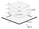
- a simplified, exploded isometric view of a reconfigurable processor module 60 in accordance with a representative embodiment of the present inventioncomprising a hybrid device incorporating a number of stacked integrated circuit die elements.
- the module 60comprises a die package 62 to which is coupled a microprocessor die 64 , memory die 66 and FPGA die 68 , all of which have a number of corresponding contact points, or holes, 70 formed throughout the area of the package 62 and various die 64 , 66 and 68 .
- a module 60 in accordance with the present inventionmay also comprise any combination of one or more of the microprocessor die 64 , memory die 66 or FPGA 68 with any other of a microprocessor die 64 , memory die 66 or FPGA die 68 .
- the contact holes 70are formed in the front side of the wafer and an insulating layer of oxide is added to separate the silicon from the metal.
- the waferis thinned to expose the through-silicon contacts.
- ADPatmospheric downstream plasma
- the oxideis etched to expose the metal. Given that this etching process etches the silicon faster, the silicon remains insulated from the contacts.
- the cache memory die 66actually serves two purposes. The first of these is its traditional role of fast access memory. However in this new assembly it is accessible by both the microprocessor 64 and the FPGA 68 with equal speed. In those applications wherein the memory 66 is tri-ported, the bandwidth for the system can be further increased. This feature clearly solves a number of the problems inherent in existing reconfigurable computing systems and the capability of utilizing the memory die 66 for other functions is potentially very important.
- FIG. 5a corresponding functional block diagram of the configuration cells 80 of the reconfigurable processor module 60 of the preceding figure is shown wherein the FPGA 70 may be totally reconfigured in one clock cycle by updating all of the configuration cells in parallel.
- a wide configuration data port 82is included to update the various logic cells 84 through an associated configuration memory 86 and buffer cell 88 .
- the buffer cells 88are preferably a portion of the memory die 66 (FIG. 4 ). In this manner, they can be loaded while the FPGA 68 comprising the logic cells 84 are in operation. This then enables the FPGA 68 to be totally reconfigured in one clock cycle with all of it configuration logic cells 84 updated in parallel.
- FIG. 4Other methods for taking advantage of the significantly increased number of connections to the cache memory die 66 (FIG. 4) may include its use to totally replace the configuration bit storage on the FPGA die 68 as well as to provide larger block random access memory (“RAM”) than can be offered within the FPGA die 68 itself.
- RAMblock random access memory
- the FPGA 68can be configured in such a way as to provide test stimulus to the microprocessor 64 , or other chips in the stack of the die package 62 during manufacture and prior to the completion of the module packaging. After test, the FPGA 68 can then be reconfigured for whatever function is desired. This then allows more thorough testing of the assembly earlier in the manufacturing process than could be otherwise achieved with traditional packaged part test systems thus reducing the costs of manufacturing.
- FPGA die 68may be included in the reconfigurable module 60 .
- inter-cell connectionscurrently limited to two dimensions of a single die, may be routed up and down the stack in three dimensions. This is not known to be possible with any other currently available stacking techniques since they all require the stacking contacts to be located on the periphery of the die. In this fashion, the number of FPGA die 68 cells that may be accessed within a specified time period is increased by up to 4 VT/3, where “V” is the propagation velocity of the wafer and “T” is the specified time of propagation.
- the disclosed technique for die interconnection used in forming the module of the present inventionis superior to other available alternatives for several reasons.
- Collocating multiple die on a planar substrateis another possible technique, but that too suffers from limited I/O connectivity and again does not allow for area connections between parts.
- Another optionwould be to fabricate a single die containing microprocessor, memory and FPGA. Such a die could use metalization layers to interconnect the three functions and achieve much of the benefits of die stacking.
Landscapes
- Engineering & Computer Science (AREA)
- Computer Hardware Design (AREA)
- Physics & Mathematics (AREA)
- General Physics & Mathematics (AREA)
- Theoretical Computer Science (AREA)
- Microelectronics & Electronic Packaging (AREA)
- General Engineering & Computer Science (AREA)
- Condensed Matter Physics & Semiconductors (AREA)
- Power Engineering (AREA)
- Design And Manufacture Of Integrated Circuits (AREA)
- Semiconductor Integrated Circuits (AREA)
- Microcomputers (AREA)
Abstract
Description
Claims (38)
Priority Applications (11)
| Application Number | Priority Date | Filing Date | Title |
|---|---|---|---|
| US10/012,057US6627985B2 (en) | 2001-12-05 | 2001-12-05 | Reconfigurable processor module comprising hybrid stacked integrated circuit die elements |
| EP02789540AEP1461715A4 (en) | 2001-12-05 | 2002-11-08 | Reconfigurable processor module comprising hybrid stacked integrated circuit die elements |
| CA002467821ACA2467821C (en) | 2001-12-05 | 2002-11-08 | Reconfigurable processor module comprising hybrid stacked integrated circuit die elements |
| PCT/US2002/035972WO2003050694A1 (en) | 2001-12-05 | 2002-11-08 | Reconfigurable processor module comprising hybrid stacked integrated circuit die elements |
| JP2003551682AJP2005512229A (en) | 2001-12-05 | 2002-11-08 | Reconfigurable processor module including hybrid stacked integrated circuit die elements |
| AU2002352582AAU2002352582A1 (en) | 2001-12-05 | 2002-11-08 | Reconfigurable processor module comprising hybrid stacked integrated circuit die elements |
| KR10-2004-7008724AKR20040072645A (en) | 2001-12-05 | 2002-11-08 | Reconfigurable processor module comprising hybrid stacked integrated circuit die elements |
| US10/452,113US6781226B2 (en) | 2001-12-05 | 2003-06-02 | Reconfigurable processor module comprising hybrid stacked integrated circuit die elements |
| US10/802,067US7126214B2 (en) | 2001-12-05 | 2004-03-16 | Reconfigurable processor module comprising hybrid stacked integrated circuit die elements |
| US11/383,149US7282951B2 (en) | 2001-12-05 | 2006-05-12 | Reconfigurable processor module comprising hybrid stacked integrated circuit die elements |
| US12/178,511USRE42035E1 (en) | 2001-12-05 | 2008-07-23 | Reconfigurable processor module comprising hybrid stacked integrated circuit die elements |
Applications Claiming Priority (1)
| Application Number | Priority Date | Filing Date | Title |
|---|---|---|---|
| US10/012,057US6627985B2 (en) | 2001-12-05 | 2001-12-05 | Reconfigurable processor module comprising hybrid stacked integrated circuit die elements |
Related Child Applications (3)
| Application Number | Title | Priority Date | Filing Date |
|---|---|---|---|
| US10/452,113ContinuationUS6781226B2 (en) | 2001-12-05 | 2003-06-02 | Reconfigurable processor module comprising hybrid stacked integrated circuit die elements |
| US10/452,113Continuation-In-PartUS6781226B2 (en) | 2001-12-05 | 2003-06-02 | Reconfigurable processor module comprising hybrid stacked integrated circuit die elements |
| US12/178,511ReissueUSRE42035E1 (en) | 2001-12-05 | 2008-07-23 | Reconfigurable processor module comprising hybrid stacked integrated circuit die elements |
Publications (2)
| Publication Number | Publication Date |
|---|---|
| US20030102495A1 US20030102495A1 (en) | 2003-06-05 |
| US6627985B2true US6627985B2 (en) | 2003-09-30 |
Family
ID=21753168
Family Applications (3)
| Application Number | Title | Priority Date | Filing Date |
|---|---|---|---|
| US10/012,057CeasedUS6627985B2 (en) | 2001-12-05 | 2001-12-05 | Reconfigurable processor module comprising hybrid stacked integrated circuit die elements |
| US10/452,113Expired - LifetimeUS6781226B2 (en) | 2001-12-05 | 2003-06-02 | Reconfigurable processor module comprising hybrid stacked integrated circuit die elements |
| US12/178,511Expired - LifetimeUSRE42035E1 (en) | 2001-12-05 | 2008-07-23 | Reconfigurable processor module comprising hybrid stacked integrated circuit die elements |
Family Applications After (2)
| Application Number | Title | Priority Date | Filing Date |
|---|---|---|---|
| US10/452,113Expired - LifetimeUS6781226B2 (en) | 2001-12-05 | 2003-06-02 | Reconfigurable processor module comprising hybrid stacked integrated circuit die elements |
| US12/178,511Expired - LifetimeUSRE42035E1 (en) | 2001-12-05 | 2008-07-23 | Reconfigurable processor module comprising hybrid stacked integrated circuit die elements |
Country Status (7)
| Country | Link |
|---|---|
| US (3) | US6627985B2 (en) |
| EP (1) | EP1461715A4 (en) |
| JP (1) | JP2005512229A (en) |
| KR (1) | KR20040072645A (en) |
| AU (1) | AU2002352582A1 (en) |
| CA (1) | CA2467821C (en) |
| WO (1) | WO2003050694A1 (en) |
Cited By (253)
| Publication number | Priority date | Publication date | Assignee | Title |
|---|---|---|---|---|
| US20040004496A1 (en)* | 2002-07-08 | 2004-01-08 | Madurawe Raminda U. | Field programmable gate array with convertibility to application specific integrated circuit |
| US20040040005A1 (en)* | 2002-01-17 | 2004-02-26 | Carison Randolph C. | Method for effectively embedding various integrated circuits within field programmable gate arrays |
| US20040073882A1 (en)* | 2002-09-04 | 2004-04-15 | Robert Osann | Emulation solution for programmable instruction DSP |
| US20040125093A1 (en)* | 2002-12-30 | 2004-07-01 | Serge Rutman | Micro-controller with integrated light modulator |
| US20040196065A1 (en)* | 2002-07-08 | 2004-10-07 | Madurawe Raminda Udaya | Programmable devices with convertibility to customizable devices |
| US20040212395A1 (en)* | 2002-07-08 | 2004-10-28 | Madurawe Raminda Udaya | Three dimensional integrated circuits |
| US20040214387A1 (en)* | 2002-07-08 | 2004-10-28 | Madurawe Raminda Udaya | Methods for fabricating three dimensional integrated circuits |
| US20040222817A1 (en)* | 2002-07-08 | 2004-11-11 | Madurawe Raminda Udaya | Alterable application specific integrated circuit (ASIC) |
| US20050067688A1 (en)* | 2003-09-26 | 2005-03-31 | Tessera, Inc. | Structure and method of making capped chips including vertical interconnects having stud bumps engaged to surfaces of said caps |
| US20050116344A1 (en)* | 2003-10-29 | 2005-06-02 | Tessera, Inc. | Microelectronic element having trace formed after bond layer |
| US20050181546A1 (en)* | 2002-07-08 | 2005-08-18 | Madurawe Raminda U. | Methods for fabricating fuse programmable three dimensional integrated circuits |
| US20050180044A1 (en)* | 2004-02-14 | 2005-08-18 | Samsung Electronics Co., Ltd. | Damping structure of a hard disk drive |
| US20050184755A1 (en)* | 2004-01-12 | 2005-08-25 | Michael Scheppler | Configurable logic component without a local configuration memory and with a parallel configuration bus |
| US20050221581A1 (en)* | 2004-03-31 | 2005-10-06 | Ramachandrarao Vijayakumar S | Wafer stacking using copper structures of substantially uniform height |
| US6991947B1 (en) | 2004-03-22 | 2006-01-31 | Tushar Gheewala | Hybrid semiconductor circuit with programmable intraconnectivity |
| US20060095716A1 (en)* | 2004-08-30 | 2006-05-04 | The Boeing Company | Super-reconfigurable fabric architecture (SURFA): a multi-FPGA parallel processing architecture for COTS hybrid computing framework |
| US20060181308A1 (en)* | 2003-12-04 | 2006-08-17 | Raminda Udaya Madurawe | Programmable structured arrays |
| US20060225020A1 (en)* | 2005-04-01 | 2006-10-05 | Anantha Chandrakasan | Methods and apparatus for 3-D FPGA design |
| US20060262587A1 (en)* | 2003-04-21 | 2006-11-23 | Elpida Memory, Inc. | Memory module and memory system |
| US20070138644A1 (en)* | 2005-12-15 | 2007-06-21 | Tessera, Inc. | Structure and method of making capped chip having discrete article assembled into vertical interconnect |
| US20070152707A1 (en)* | 2004-01-05 | 2007-07-05 | Madurawe Raminda U | Integrated circuits with RAM and ROM fabrication options |
| US20070152708A1 (en)* | 2002-07-08 | 2007-07-05 | Madurawe Raminda U | MPGA products based on a prototype FPGA |
| US7265440B2 (en) | 2003-06-16 | 2007-09-04 | Tessera Technologies Hungary Kft. | Methods and apparatus for packaging integrated circuit devices |
| US20070210826A1 (en)* | 2006-03-08 | 2007-09-13 | Madurawe Raminda U | Programmable logic devices comprising time multiplexed programmable interconnect |
| US7327159B1 (en)* | 2005-11-28 | 2008-02-05 | Lattice Semiconductor Corporation | Interface block architectures |
| US20080067594A1 (en)* | 2002-07-08 | 2008-03-20 | Madurawe Raminda U | Insulated-gate field-effect thin film transistors |
| US20080074144A1 (en)* | 2002-01-17 | 2008-03-27 | Volkan Ozguz | Field programmable gate array utilizing dedicated memory stacks in a vertical layer format |
| US20080106953A1 (en)* | 2004-05-17 | 2008-05-08 | Madurawe Raminda U | Multi-port memory devices |
| US7479398B2 (en) | 2003-07-03 | 2009-01-20 | Tessera Technologies Hungary Kft. | Methods and apparatus for packaging integrated circuit devices |
| US20090039917A1 (en)* | 2002-10-21 | 2009-02-12 | Raminda Udaya Madurawe | Programmable Interconnect Structures |
| US20090128189A1 (en)* | 2007-11-19 | 2009-05-21 | Raminda Udaya Madurawe | Three dimensional programmable devices |
| US20090129174A1 (en)* | 2007-11-19 | 2009-05-21 | Raminda Madurawe | Multi-port thin-film memory devices |
| US20090128188A1 (en)* | 2007-11-19 | 2009-05-21 | Raminda Udaya Madurawe | Pad invariant FPGA and ASIC devices |
| US20090146189A1 (en)* | 2007-11-19 | 2009-06-11 | Raminda Udaya Madurawe | Pads and pin-outs in three dimensional integrated circuits |
| US20090167350A1 (en)* | 2007-12-26 | 2009-07-02 | Raminda Madurawe | Programmable logic based latches and shift registers |
| US20090167348A1 (en)* | 2007-12-26 | 2009-07-02 | Nij Dorairaj | Programmable latch based multiplier |
| US20090167347A1 (en)* | 2007-12-26 | 2009-07-02 | Nij Dorairaj | Using programmable latch to implement logic |
| US20090167349A1 (en)* | 2007-12-26 | 2009-07-02 | Raminda Madurawe | Programmable logic based latches and shift registers |
| US7566955B2 (en) | 2001-08-28 | 2009-07-28 | Tessera, Inc. | High-frequency chip packages |
| US20090196086A1 (en)* | 2008-02-05 | 2009-08-06 | Pelley Perry H | High bandwidth cache-to-processing unit communication in a multiple processor/cache system |
| US20100123477A1 (en)* | 2008-11-20 | 2010-05-20 | Shih-Wei Sun | Programmable array module |
| US7936062B2 (en) | 2006-01-23 | 2011-05-03 | Tessera Technologies Ireland Limited | Wafer level chip packaging |
| US20110101537A1 (en)* | 2009-10-29 | 2011-05-05 | International Business Machines Corporation | Hybrid bonding interface for 3-dimensional chip integration |
| US8143095B2 (en) | 2005-03-22 | 2012-03-27 | Tessera, Inc. | Sequential fabrication of vertical conductive interconnects in capped chips |
| US8159265B1 (en) | 2010-11-16 | 2012-04-17 | Raminda Udaya Madurawe | Memory for metal configurable integrated circuits |
| US8159268B1 (en) | 2010-11-16 | 2012-04-17 | Raminda Udaya Madurawe | Interconnect structures for metal configurable integrated circuits |
| US8159266B1 (en) | 2010-11-16 | 2012-04-17 | Raminda Udaya Madurawe | Metal configurable integrated circuits |
| US20120193806A1 (en)* | 2009-04-14 | 2012-08-02 | Zvi Or-Bach | 3d semiconductor device |
| US20120299640A1 (en)* | 2009-11-12 | 2012-11-29 | International Business Machines Corporation | Integrated Circuit Die Stacks Having Initially Identical Dies Personalized With Fuses |
| EP2605105A2 (en) | 2011-12-16 | 2013-06-19 | SRC Computers, LLC | Mobile electronic devices utilizing reconfigurable processing techniques to enable higher speed applications with lowered power consumption |
| US8481425B2 (en) | 2011-05-16 | 2013-07-09 | United Microelectronics Corp. | Method for fabricating through-silicon via structure |
| US8519515B2 (en) | 2011-04-13 | 2013-08-27 | United Microlectronics Corp. | TSV structure and method for forming the same |
| US8518823B2 (en) | 2011-12-23 | 2013-08-27 | United Microelectronics Corp. | Through silicon via and method of forming the same |
| US8525296B1 (en) | 2012-06-26 | 2013-09-03 | United Microelectronics Corp. | Capacitor structure and method of forming the same |
| US8604605B2 (en) | 2007-01-05 | 2013-12-10 | Invensas Corp. | Microelectronic assembly with multi-layer support structure |
| US8609529B2 (en) | 2012-02-01 | 2013-12-17 | United Microelectronics Corp. | Fabrication method and structure of through silicon via |
| US8691688B2 (en) | 2012-06-18 | 2014-04-08 | United Microelectronics Corp. | Method of manufacturing semiconductor structure |
| US8691600B2 (en) | 2012-05-02 | 2014-04-08 | United Microelectronics Corp. | Method for testing through-silicon-via (TSV) structures |
| US8716104B1 (en) | 2012-12-20 | 2014-05-06 | United Microelectronics Corp. | Method of fabricating isolation structure |
| US8822336B2 (en) | 2011-06-16 | 2014-09-02 | United Microelectronics Corp. | Through-silicon via forming method |
| US8828745B2 (en) | 2011-07-06 | 2014-09-09 | United Microelectronics Corp. | Method for manufacturing through-silicon via |
| US8884398B2 (en) | 2013-04-01 | 2014-11-11 | United Microelectronics Corp. | Anti-fuse structure and programming method thereof |
| US8900996B2 (en) | 2012-06-21 | 2014-12-02 | United Microelectronics Corp. | Through silicon via structure and method of fabricating the same |
| US8912844B2 (en) | 2012-10-09 | 2014-12-16 | United Microelectronics Corp. | Semiconductor structure and method for reducing noise therein |
| US8916471B1 (en) | 2013-08-26 | 2014-12-23 | United Microelectronics Corp. | Method for forming semiconductor structure having through silicon via for signal and shielding structure |
| US8984463B2 (en) | 2012-11-28 | 2015-03-17 | Qualcomm Incorporated | Data transfer across power domains |
| US9024416B2 (en) | 2013-08-12 | 2015-05-05 | United Microelectronics Corp. | Semiconductor structure |
| US9035457B2 (en) | 2012-11-29 | 2015-05-19 | United Microelectronics Corp. | Substrate with integrated passive devices and method of manufacturing the same |
| US9041448B2 (en) | 2013-03-05 | 2015-05-26 | Qualcomm Incorporated | Flip-flops in a monolithic three-dimensional (3D) integrated circuit (IC) (3DIC) and related methods |
| US9048223B2 (en) | 2013-09-03 | 2015-06-02 | United Microelectronics Corp. | Package structure having silicon through vias connected to ground potential |
| US9064077B2 (en)* | 2012-11-28 | 2015-06-23 | Qualcomm Incorporated | 3D floorplanning using 2D and 3D blocks |
| US9087169B2 (en) | 2008-09-14 | 2015-07-21 | Raminda U. Madurawe | Automated metal pattern generation for integrated circuits |
| US9117804B2 (en) | 2013-09-13 | 2015-08-25 | United Microelectronics Corporation | Interposer structure and manufacturing method thereof |
| US9123730B2 (en) | 2013-07-11 | 2015-09-01 | United Microelectronics Corp. | Semiconductor device having through silicon trench shielding structure surrounding RF circuit |
| US9171608B2 (en) | 2013-03-15 | 2015-10-27 | Qualcomm Incorporated | Three-dimensional (3D) memory cell separation among 3D integrated circuit (IC) tiers, and related 3D integrated circuits (3DICS), 3DIC processor cores, and methods |
| US9177890B2 (en) | 2013-03-07 | 2015-11-03 | Qualcomm Incorporated | Monolithic three dimensional integration of semiconductor integrated circuits |
| US9275933B2 (en) | 2012-06-19 | 2016-03-01 | United Microelectronics Corp. | Semiconductor device |
| US9287173B2 (en) | 2013-05-23 | 2016-03-15 | United Microelectronics Corp. | Through silicon via and process thereof |
| US9343359B2 (en) | 2013-12-25 | 2016-05-17 | United Microelectronics Corp. | Integrated structure and method for fabricating the same |
| US9536840B2 (en) | 2013-02-12 | 2017-01-03 | Qualcomm Incorporated | Three-dimensional (3-D) integrated circuits (3DICS) with graphene shield, and related components and methods |
| US9753769B2 (en) | 2013-01-28 | 2017-09-05 | Samsung Electronics Co., Ltd. | Apparatus and method for sharing function logic between functional units, and reconfigurable processor thereof |
| US10043781B2 (en) | 2009-10-12 | 2018-08-07 | Monolithic 3D Inc. | 3D semiconductor device and structure |
| US10115663B2 (en) | 2012-12-29 | 2018-10-30 | Monolithic 3D Inc. | 3D semiconductor device and structure |
| US10127344B2 (en) | 2013-04-15 | 2018-11-13 | Monolithic 3D Inc. | Automation for monolithic 3D devices |
| US10157909B2 (en) | 2009-10-12 | 2018-12-18 | Monolithic 3D Inc. | 3D semiconductor device and structure |
| US10217667B2 (en) | 2011-06-28 | 2019-02-26 | Monolithic 3D Inc. | 3D semiconductor device, fabrication method and system |
| US10224279B2 (en) | 2013-03-15 | 2019-03-05 | Monolithic 3D Inc. | Semiconductor device and structure |
| US10290682B2 (en) | 2010-10-11 | 2019-05-14 | Monolithic 3D Inc. | 3D IC semiconductor device and structure with stacked memory |
| US10297586B2 (en) | 2015-03-09 | 2019-05-21 | Monolithic 3D Inc. | Methods for processing a 3D semiconductor device |
| US10325651B2 (en) | 2013-03-11 | 2019-06-18 | Monolithic 3D Inc. | 3D semiconductor device with stacked memory |
| US10340203B2 (en) | 2014-02-07 | 2019-07-02 | United Microelectronics Corp. | Semiconductor structure with through silicon via and method for fabricating and testing the same |
| US10354995B2 (en) | 2009-10-12 | 2019-07-16 | Monolithic 3D Inc. | Semiconductor memory device and structure |
| US10355121B2 (en) | 2013-03-11 | 2019-07-16 | Monolithic 3D Inc. | 3D semiconductor device with stacked memory |
| US10366970B2 (en) | 2009-10-12 | 2019-07-30 | Monolithic 3D Inc. | 3D semiconductor device and structure |
| US10381328B2 (en) | 2015-04-19 | 2019-08-13 | Monolithic 3D Inc. | Semiconductor device and structure |
| US10388863B2 (en) | 2009-10-12 | 2019-08-20 | Monolithic 3D Inc. | 3D memory device and structure |
| US10388568B2 (en) | 2011-06-28 | 2019-08-20 | Monolithic 3D Inc. | 3D semiconductor device and system |
| US10418369B2 (en) | 2015-10-24 | 2019-09-17 | Monolithic 3D Inc. | Multi-level semiconductor memory device and structure |
| US10497713B2 (en) | 2010-11-18 | 2019-12-03 | Monolithic 3D Inc. | 3D semiconductor memory device and structure |
| US10515981B2 (en) | 2015-09-21 | 2019-12-24 | Monolithic 3D Inc. | Multilevel semiconductor device and structure with memory |
| US10522225B1 (en) | 2015-10-02 | 2019-12-31 | Monolithic 3D Inc. | Semiconductor device with non-volatile memory |
| US10600888B2 (en) | 2012-04-09 | 2020-03-24 | Monolithic 3D Inc. | 3D semiconductor device |
| US10600657B2 (en) | 2012-12-29 | 2020-03-24 | Monolithic 3D Inc | 3D semiconductor device and structure |
| US10651054B2 (en) | 2012-12-29 | 2020-05-12 | Monolithic 3D Inc. | 3D semiconductor device and structure |
| US10679977B2 (en) | 2010-10-13 | 2020-06-09 | Monolithic 3D Inc. | 3D microdisplay device and structure |
| US10825779B2 (en) | 2015-04-19 | 2020-11-03 | Monolithic 3D Inc. | 3D semiconductor device and structure |
| US10833108B2 (en) | 2010-10-13 | 2020-11-10 | Monolithic 3D Inc. | 3D microdisplay device and structure |
| US10840239B2 (en) | 2014-08-26 | 2020-11-17 | Monolithic 3D Inc. | 3D semiconductor device and structure |
| US10847540B2 (en) | 2015-10-24 | 2020-11-24 | Monolithic 3D Inc. | 3D semiconductor memory device and structure |
| WO2020236379A1 (en) | 2019-05-21 | 2020-11-26 | Arbor Company Lllp | Systems and methods for integrating batteries with stacked integrated circuit die elements |
| US10892169B2 (en) | 2012-12-29 | 2021-01-12 | Monolithic 3D Inc. | 3D semiconductor device and structure |
| US10892016B1 (en) | 2019-04-08 | 2021-01-12 | Monolithic 3D Inc. | 3D memory semiconductor devices and structures |
| US10896931B1 (en) | 2010-10-11 | 2021-01-19 | Monolithic 3D Inc. | 3D semiconductor device and structure |
| US10903089B1 (en) | 2012-12-29 | 2021-01-26 | Monolithic 3D Inc. | 3D semiconductor device and structure |
| US10910364B2 (en) | 2009-10-12 | 2021-02-02 | Monolitaic 3D Inc. | 3D semiconductor device |
| US10943934B2 (en) | 2010-10-13 | 2021-03-09 | Monolithic 3D Inc. | Multilevel semiconductor device and structure |
| US10978501B1 (en) | 2010-10-13 | 2021-04-13 | Monolithic 3D Inc. | Multilevel semiconductor device and structure with waveguides |
| US10998374B1 (en) | 2010-10-13 | 2021-05-04 | Monolithic 3D Inc. | Multilevel semiconductor device and structure |
| US11004719B1 (en) | 2010-11-18 | 2021-05-11 | Monolithic 3D Inc. | Methods for producing a 3D semiconductor memory device and structure |
| US11004694B1 (en) | 2012-12-29 | 2021-05-11 | Monolithic 3D Inc. | 3D semiconductor device and structure |
| US11011507B1 (en) | 2015-04-19 | 2021-05-18 | Monolithic 3D Inc. | 3D semiconductor device and structure |
| US11018116B2 (en) | 2012-12-22 | 2021-05-25 | Monolithic 3D Inc. | Method to form a 3D semiconductor device and structure |
| US11018042B1 (en) | 2010-11-18 | 2021-05-25 | Monolithic 3D Inc. | 3D semiconductor memory device and structure |
| US11018191B1 (en) | 2010-10-11 | 2021-05-25 | Monolithic 3D Inc. | 3D semiconductor device and structure |
| US11018156B2 (en) | 2019-04-08 | 2021-05-25 | Monolithic 3D Inc. | 3D memory semiconductor devices and structures |
| US11018133B2 (en) | 2009-10-12 | 2021-05-25 | Monolithic 3D Inc. | 3D integrated circuit |
| US11024673B1 (en) | 2010-10-11 | 2021-06-01 | Monolithic 3D Inc. | 3D semiconductor device and structure |
| US11030371B2 (en) | 2013-04-15 | 2021-06-08 | Monolithic 3D Inc. | Automation for monolithic 3D devices |
| US11031275B2 (en) | 2010-11-18 | 2021-06-08 | Monolithic 3D Inc. | 3D semiconductor device and structure with memory |
| US11031394B1 (en) | 2014-01-28 | 2021-06-08 | Monolithic 3D Inc. | 3D semiconductor device and structure |
| US11043523B1 (en) | 2010-10-13 | 2021-06-22 | Monolithic 3D Inc. | Multilevel semiconductor device and structure with image sensors |
| US11056468B1 (en) | 2015-04-19 | 2021-07-06 | Monolithic 3D Inc. | 3D semiconductor device and structure |
| US11063071B1 (en) | 2010-10-13 | 2021-07-13 | Monolithic 3D Inc. | Multilevel semiconductor device and structure with waveguides |
| US11063024B1 (en) | 2012-12-22 | 2021-07-13 | Monlithic 3D Inc. | Method to form a 3D semiconductor device and structure |
| US11088050B2 (en) | 2012-04-09 | 2021-08-10 | Monolithic 3D Inc. | 3D semiconductor device with isolation layers |
| US11088130B2 (en) | 2014-01-28 | 2021-08-10 | Monolithic 3D Inc. | 3D semiconductor device and structure |
| US11087995B1 (en) | 2012-12-29 | 2021-08-10 | Monolithic 3D Inc. | 3D semiconductor device and structure |
| US11094576B1 (en) | 2010-11-18 | 2021-08-17 | Monolithic 3D Inc. | Methods for producing a 3D semiconductor memory device and structure |
| US11107808B1 (en) | 2014-01-28 | 2021-08-31 | Monolithic 3D Inc. | 3D semiconductor device and structure |
| US11107721B2 (en) | 2010-11-18 | 2021-08-31 | Monolithic 3D Inc. | 3D semiconductor device and structure with NAND logic |
| US11114464B2 (en) | 2015-10-24 | 2021-09-07 | Monolithic 3D Inc. | 3D semiconductor device and structure |
| US11114427B2 (en) | 2015-11-07 | 2021-09-07 | Monolithic 3D Inc. | 3D semiconductor processor and memory device and structure |
| US11121021B2 (en) | 2010-11-18 | 2021-09-14 | Monolithic 3D Inc. | 3D semiconductor device and structure |
| US11133344B2 (en) | 2010-10-13 | 2021-09-28 | Monolithic 3D Inc. | Multilevel semiconductor device and structure with image sensors |
| US11158652B1 (en) | 2019-04-08 | 2021-10-26 | Monolithic 3D Inc. | 3D memory semiconductor devices and structures |
| US11158674B2 (en) | 2010-10-11 | 2021-10-26 | Monolithic 3D Inc. | Method to produce a 3D semiconductor device and structure |
| US11163112B2 (en) | 2010-10-13 | 2021-11-02 | Monolithic 3D Inc. | Multilevel semiconductor device and structure with electromagnetic modulators |
| US11164811B2 (en) | 2012-04-09 | 2021-11-02 | Monolithic 3D Inc. | 3D semiconductor device with isolation layers and oxide-to-oxide bonding |
| US11164898B2 (en) | 2010-10-13 | 2021-11-02 | Monolithic 3D Inc. | Multilevel semiconductor device and structure |
| US11164770B1 (en) | 2010-11-18 | 2021-11-02 | Monolithic 3D Inc. | Method for producing a 3D semiconductor memory device and structure |
| US11177140B2 (en) | 2012-12-29 | 2021-11-16 | Monolithic 3D Inc. | 3D semiconductor device and structure |
| US11211279B2 (en) | 2010-11-18 | 2021-12-28 | Monolithic 3D Inc. | Method for processing a 3D integrated circuit and structure |
| US11217565B2 (en) | 2012-12-22 | 2022-01-04 | Monolithic 3D Inc. | Method to form a 3D semiconductor device and structure |
| US11227897B2 (en) | 2010-10-11 | 2022-01-18 | Monolithic 3D Inc. | Method for producing a 3D semiconductor memory device and structure |
| US11251149B2 (en) | 2016-10-10 | 2022-02-15 | Monolithic 3D Inc. | 3D memory device and structure |
| US11257867B1 (en) | 2010-10-11 | 2022-02-22 | Monolithic 3D Inc. | 3D semiconductor device and structure with oxide bonds |
| US11270055B1 (en) | 2013-04-15 | 2022-03-08 | Monolithic 3D Inc. | Automation for monolithic 3D devices |
| US11296115B1 (en) | 2015-10-24 | 2022-04-05 | Monolithic 3D Inc. | 3D semiconductor device and structure |
| US11296106B2 (en) | 2019-04-08 | 2022-04-05 | Monolithic 3D Inc. | 3D memory semiconductor devices and structures |
| US11309292B2 (en) | 2012-12-22 | 2022-04-19 | Monolithic 3D Inc. | 3D semiconductor device and structure with metal layers |
| US11315980B1 (en) | 2010-10-11 | 2022-04-26 | Monolithic 3D Inc. | 3D semiconductor device and structure with transistors |
| US11329059B1 (en) | 2016-10-10 | 2022-05-10 | Monolithic 3D Inc. | 3D memory devices and structures with thinned single crystal substrates |
| US11327227B2 (en) | 2010-10-13 | 2022-05-10 | Monolithic 3D Inc. | Multilevel semiconductor device and structure with electromagnetic modulators |
| US11341309B1 (en) | 2013-04-15 | 2022-05-24 | Monolithic 3D Inc. | Automation for monolithic 3D devices |
| US11355380B2 (en) | 2010-11-18 | 2022-06-07 | Monolithic 3D Inc. | Methods for producing 3D semiconductor memory device and structure utilizing alignment marks |
| US11355381B2 (en) | 2010-11-18 | 2022-06-07 | Monolithic 3D Inc. | 3D semiconductor memory device and structure |
| US11374118B2 (en) | 2009-10-12 | 2022-06-28 | Monolithic 3D Inc. | Method to form a 3D integrated circuit |
| US11398569B2 (en) | 2013-03-12 | 2022-07-26 | Monolithic 3D Inc. | 3D semiconductor device and structure |
| US11404466B2 (en) | 2010-10-13 | 2022-08-02 | Monolithic 3D Inc. | Multilevel semiconductor device and structure with image sensors |
| US11410912B2 (en) | 2012-04-09 | 2022-08-09 | Monolithic 3D Inc. | 3D semiconductor device with vias and isolation layers |
| US11430668B2 (en) | 2012-12-29 | 2022-08-30 | Monolithic 3D Inc. | 3D semiconductor device and structure with bonding |
| US11430667B2 (en) | 2012-12-29 | 2022-08-30 | Monolithic 3D Inc. | 3D semiconductor device and structure with bonding |
| US11437368B2 (en) | 2010-10-13 | 2022-09-06 | Monolithic 3D Inc. | Multilevel semiconductor device and structure with oxide bonding |
| US11443971B2 (en) | 2010-11-18 | 2022-09-13 | Monolithic 3D Inc. | 3D semiconductor device and structure with memory |
| US11469271B2 (en) | 2010-10-11 | 2022-10-11 | Monolithic 3D Inc. | Method to produce 3D semiconductor devices and structures with memory |
| US11476181B1 (en) | 2012-04-09 | 2022-10-18 | Monolithic 3D Inc. | 3D semiconductor device and structure with metal layers |
| US11482440B2 (en) | 2010-12-16 | 2022-10-25 | Monolithic 3D Inc. | 3D semiconductor device and structure with a built-in test circuit for repairing faulty circuits |
| US11482438B2 (en) | 2010-11-18 | 2022-10-25 | Monolithic 3D Inc. | Methods for producing a 3D semiconductor memory device and structure |
| US11482439B2 (en) | 2010-11-18 | 2022-10-25 | Monolithic 3D Inc. | Methods for producing a 3D semiconductor memory device comprising charge trap junction-less transistors |
| US11487928B2 (en) | 2013-04-15 | 2022-11-01 | Monolithic 3D Inc. | Automation for monolithic 3D devices |
| US11495484B2 (en) | 2010-11-18 | 2022-11-08 | Monolithic 3D Inc. | 3D semiconductor devices and structures with at least two single-crystal layers |
| US11508605B2 (en) | 2010-11-18 | 2022-11-22 | Monolithic 3D Inc. | 3D semiconductor memory device and structure |
| US11521888B2 (en) | 2010-11-18 | 2022-12-06 | Monolithic 3D Inc. | 3D semiconductor device and structure with high-k metal gate transistors |
| US11569117B2 (en) | 2010-11-18 | 2023-01-31 | Monolithic 3D Inc. | 3D semiconductor device and structure with single-crystal layers |
| US11574109B1 (en) | 2013-04-15 | 2023-02-07 | Monolithic 3D Inc | Automation methods for 3D integrated circuits and devices |
| US11594473B2 (en) | 2012-04-09 | 2023-02-28 | Monolithic 3D Inc. | 3D semiconductor device and structure with metal layers and a connective path |
| US11600667B1 (en) | 2010-10-11 | 2023-03-07 | Monolithic 3D Inc. | Method to produce 3D semiconductor devices and structures with memory |
| US11605663B2 (en) | 2010-10-13 | 2023-03-14 | Monolithic 3D Inc. | Multilevel semiconductor device and structure with image sensors and wafer bonding |
| US11610802B2 (en) | 2010-11-18 | 2023-03-21 | Monolithic 3D Inc. | Method for producing a 3D semiconductor device and structure with single crystal transistors and metal gate electrodes |
| US11615977B2 (en) | 2010-11-18 | 2023-03-28 | Monolithic 3D Inc. | 3D semiconductor memory device and structure |
| US11616004B1 (en) | 2012-04-09 | 2023-03-28 | Monolithic 3D Inc. | 3D semiconductor device and structure with metal layers and a connective path |
| US11694944B1 (en) | 2012-04-09 | 2023-07-04 | Monolithic 3D Inc. | 3D semiconductor device and structure with metal layers and a connective path |
| US11694922B2 (en) | 2010-10-13 | 2023-07-04 | Monolithic 3D Inc. | Multilevel semiconductor device and structure with oxide bonding |
| US11711928B2 (en) | 2016-10-10 | 2023-07-25 | Monolithic 3D Inc. | 3D memory devices and structures with control circuits |
| US11720736B2 (en) | 2013-04-15 | 2023-08-08 | Monolithic 3D Inc. | Automation methods for 3D integrated circuits and devices |
| US11735462B2 (en) | 2010-11-18 | 2023-08-22 | Monolithic 3D Inc. | 3D semiconductor device and structure with single-crystal layers |
| US11735501B1 (en) | 2012-04-09 | 2023-08-22 | Monolithic 3D Inc. | 3D semiconductor device and structure with metal layers and a connective path |
| US11763864B2 (en) | 2019-04-08 | 2023-09-19 | Monolithic 3D Inc. | 3D memory semiconductor devices and structures with bit-line pillars |
| US11784082B2 (en) | 2010-11-18 | 2023-10-10 | Monolithic 3D Inc. | 3D semiconductor device and structure with bonding |
| US11784169B2 (en) | 2012-12-22 | 2023-10-10 | Monolithic 3D Inc. | 3D semiconductor device and structure with metal layers |
| US11804396B2 (en) | 2010-11-18 | 2023-10-31 | Monolithic 3D Inc. | Methods for producing a 3D semiconductor device and structure with memory cells and multiple metal layers |
| US11812620B2 (en) | 2016-10-10 | 2023-11-07 | Monolithic 3D Inc. | 3D DRAM memory devices and structures with control circuits |
| US11855100B2 (en) | 2010-10-13 | 2023-12-26 | Monolithic 3D Inc. | Multilevel semiconductor device and structure with oxide bonding |
| US11854857B1 (en) | 2010-11-18 | 2023-12-26 | Monolithic 3D Inc. | Methods for producing a 3D semiconductor device and structure with memory cells and multiple metal layers |
| US11855114B2 (en) | 2010-10-13 | 2023-12-26 | Monolithic 3D Inc. | Multilevel semiconductor device and structure with image sensors and wafer bonding |
| US11862503B2 (en) | 2010-11-18 | 2024-01-02 | Monolithic 3D Inc. | Method for producing a 3D semiconductor device and structure with memory cells and multiple metal layers |
| US11869965B2 (en) | 2013-03-11 | 2024-01-09 | Monolithic 3D Inc. | 3D semiconductor device and structure with metal layers and memory cells |
| US11869915B2 (en) | 2010-10-13 | 2024-01-09 | Monolithic 3D Inc. | Multilevel semiconductor device and structure with image sensors and wafer bonding |
| US11869591B2 (en) | 2016-10-10 | 2024-01-09 | Monolithic 3D Inc. | 3D memory devices and structures with control circuits |
| US11881443B2 (en) | 2012-04-09 | 2024-01-23 | Monolithic 3D Inc. | 3D semiconductor device and structure with metal layers and a connective path |
| US11901210B2 (en) | 2010-11-18 | 2024-02-13 | Monolithic 3D Inc. | 3D semiconductor device and structure with memory |
| US11916045B2 (en) | 2012-12-22 | 2024-02-27 | Monolithic 3D Inc. | 3D semiconductor device and structure with metal layers |
| US11923230B1 (en) | 2010-11-18 | 2024-03-05 | Monolithic 3D Inc. | 3D semiconductor device and structure with bonding |
| US11923374B2 (en) | 2013-03-12 | 2024-03-05 | Monolithic 3D Inc. | 3D semiconductor device and structure with metal layers |
| US11929372B2 (en) | 2010-10-13 | 2024-03-12 | Monolithic 3D Inc. | Multilevel semiconductor device and structure with image sensors and wafer bonding |
| US11930648B1 (en) | 2016-10-10 | 2024-03-12 | Monolithic 3D Inc. | 3D memory devices and structures with metal layers |
| US11935949B1 (en) | 2013-03-11 | 2024-03-19 | Monolithic 3D Inc. | 3D semiconductor device and structure with metal layers and memory cells |
| US11937422B2 (en) | 2015-11-07 | 2024-03-19 | Monolithic 3D Inc. | Semiconductor memory device and structure |
| US11956952B2 (en) | 2015-08-23 | 2024-04-09 | Monolithic 3D Inc. | Semiconductor memory device and structure |
| US11961827B1 (en) | 2012-12-22 | 2024-04-16 | Monolithic 3D Inc. | 3D semiconductor device and structure with metal layers |
| US11967583B2 (en) | 2012-12-22 | 2024-04-23 | Monolithic 3D Inc. | 3D semiconductor device and structure with metal layers |
| US11978731B2 (en) | 2015-09-21 | 2024-05-07 | Monolithic 3D Inc. | Method to produce a multi-level semiconductor memory device and structure |
| US11984438B2 (en) | 2010-10-13 | 2024-05-14 | Monolithic 3D Inc. | Multilevel semiconductor device and structure with oxide bonding |
| US11984445B2 (en) | 2009-10-12 | 2024-05-14 | Monolithic 3D Inc. | 3D semiconductor devices and structures with metal layers |
| US11991884B1 (en) | 2015-10-24 | 2024-05-21 | Monolithic 3D Inc. | 3D semiconductor device and structure with logic and memory |
| US12016181B2 (en) | 2015-10-24 | 2024-06-18 | Monolithic 3D Inc. | 3D semiconductor device and structure with logic and memory |
| US12027518B1 (en) | 2009-10-12 | 2024-07-02 | Monolithic 3D Inc. | 3D semiconductor devices and structures with metal layers |
| US12033884B2 (en) | 2010-11-18 | 2024-07-09 | Monolithic 3D Inc. | Methods for producing a 3D semiconductor device and structure with memory cells and multiple metal layers |
| US12035531B2 (en) | 2015-10-24 | 2024-07-09 | Monolithic 3D Inc. | 3D semiconductor device and structure with logic and memory |
| US12051674B2 (en) | 2012-12-22 | 2024-07-30 | Monolithic 3D Inc. | 3D semiconductor device and structure with metal layers |
| US12068187B2 (en) | 2010-11-18 | 2024-08-20 | Monolithic 3D Inc. | 3D semiconductor device and structure with bonding and DRAM memory cells |
| US12080743B2 (en) | 2010-10-13 | 2024-09-03 | Monolithic 3D Inc. | Multilevel semiconductor device and structure with image sensors and wafer bonding |
| US12094892B2 (en) | 2010-10-13 | 2024-09-17 | Monolithic 3D Inc. | 3D micro display device and structure |
| US12094829B2 (en) | 2014-01-28 | 2024-09-17 | Monolithic 3D Inc. | 3D semiconductor device and structure |
| US12094965B2 (en) | 2013-03-11 | 2024-09-17 | Monolithic 3D Inc. | 3D semiconductor device and structure with metal layers and memory cells |
| US12100611B2 (en) | 2010-11-18 | 2024-09-24 | Monolithic 3D Inc. | Methods for producing a 3D semiconductor device and structure with memory cells and multiple metal layers |
| US12100646B2 (en) | 2013-03-12 | 2024-09-24 | Monolithic 3D Inc. | 3D semiconductor device and structure with metal layers |
| US12100658B2 (en) | 2015-09-21 | 2024-09-24 | Monolithic 3D Inc. | Method to produce a 3D multilayer semiconductor device and structure |
| US12120880B1 (en) | 2015-10-24 | 2024-10-15 | Monolithic 3D Inc. | 3D semiconductor device and structure with logic and memory |
| US12125737B1 (en) | 2010-11-18 | 2024-10-22 | Monolithic 3D Inc. | 3D semiconductor device and structure with metal layers and memory cells |
| US12136562B2 (en) | 2010-11-18 | 2024-11-05 | Monolithic 3D Inc. | 3D semiconductor device and structure with single-crystal layers |
| US12144190B2 (en) | 2010-11-18 | 2024-11-12 | Monolithic 3D Inc. | 3D semiconductor device and structure with bonding and memory cells preliminary class |
| US12154817B1 (en) | 2010-11-18 | 2024-11-26 | Monolithic 3D Inc. | Methods for producing a 3D semiconductor memory device and structure |
| US12178055B2 (en) | 2015-09-21 | 2024-12-24 | Monolithic 3D Inc. | 3D semiconductor memory devices and structures |
| US12219769B2 (en) | 2015-10-24 | 2025-02-04 | Monolithic 3D Inc. | 3D semiconductor device and structure with logic and memory |
| US12225704B2 (en) | 2016-10-10 | 2025-02-11 | Monolithic 3D Inc. | 3D memory devices and structures with memory arrays and metal layers |
| US12225711B2 (en) | 2011-01-14 | 2025-02-11 | Semiconductor Energy Laboratory Co., Ltd. | Semiconductor device comprising wiring layer over driver circuit |
| US12243765B2 (en) | 2010-11-18 | 2025-03-04 | Monolithic 3D Inc. | 3D semiconductor device and structure with metal layers and memory cells |
| US12249538B2 (en) | 2012-12-29 | 2025-03-11 | Monolithic 3D Inc. | 3D semiconductor device and structure including power distribution grids |
| US12250830B2 (en) | 2015-09-21 | 2025-03-11 | Monolithic 3D Inc. | 3D semiconductor memory devices and structures |
| US12272586B2 (en) | 2010-11-18 | 2025-04-08 | Monolithic 3D Inc. | 3D semiconductor memory device and structure with memory and metal layers |
| US12360310B2 (en) | 2010-10-13 | 2025-07-15 | Monolithic 3D Inc. | Multilevel semiconductor device and structure with oxide bonding |
| US12362219B2 (en) | 2010-11-18 | 2025-07-15 | Monolithic 3D Inc. | 3D semiconductor memory device and structure |
Families Citing this family (43)
| Publication number | Priority date | Publication date | Assignee | Title |
|---|---|---|---|---|
| US9092595B2 (en)* | 1997-10-08 | 2015-07-28 | Pact Xpp Technologies Ag | Multiprocessor having associated RAM units |
| US7030488B2 (en)* | 2001-10-30 | 2006-04-18 | Intel Corporation | Packaged combination memory for electronic devices |
| US7126214B2 (en)* | 2001-12-05 | 2006-10-24 | Arbor Company Llp | Reconfigurable processor module comprising hybrid stacked integrated circuit die elements |
| US6627985B2 (en)* | 2001-12-05 | 2003-09-30 | Arbor Company Llp | Reconfigurable processor module comprising hybrid stacked integrated circuit die elements |
| US6917219B2 (en)* | 2003-03-12 | 2005-07-12 | Xilinx, Inc. | Multi-chip programmable logic device having configurable logic circuitry and configuration data storage on different dice |
| JP4045506B2 (en)* | 2004-01-21 | 2008-02-13 | セイコーエプソン株式会社 | Stacked semiconductor memory device |
| AU2005244420A1 (en)* | 2004-05-13 | 2005-11-24 | Basf Aktiengesellschaft | Triazolopyrimidine derivative-based fungicide mixtures |
| US7556775B2 (en)* | 2004-05-25 | 2009-07-07 | The United States Of America As Represented By The Secretary Of The Navy | Microelectro-mechanical chemical sensor |
| US7459772B2 (en)* | 2004-09-29 | 2008-12-02 | Actel Corporation | Face-to-face bonded I/O circuit die and functional logic circuit die system |
| US7301242B2 (en)* | 2004-11-04 | 2007-11-27 | Tabula, Inc. | Programmable system in package |
| WO2006072142A1 (en)* | 2005-01-06 | 2006-07-13 | Justin Martin Spangaro | A reprogrammable integrated circuit |
| US8201124B1 (en) | 2005-03-15 | 2012-06-12 | Tabula, Inc. | System in package and method of creating system in package |
| US7382154B2 (en)* | 2005-10-03 | 2008-06-03 | Honeywell International Inc. | Reconfigurable network on a chip |
| US8093717B2 (en) | 2005-12-09 | 2012-01-10 | Intel Corporation | Microstrip spacer for stacked chip scale packages, methods of making same, methods of operating same, and systems containing same |
| US7714450B2 (en) | 2006-03-27 | 2010-05-11 | Marvell International Technology Ltd. | On-die bond wires system and method for enhancing routability of a redistribution layer |
| KR100883655B1 (en)* | 2006-12-04 | 2009-02-18 | 삼성전자주식회사 | Context exchange system and method with reconfigurable processor |
| EP2191007B1 (en) | 2007-04-20 | 2019-06-05 | Becton, Dickinson and Company | Hydrogel compositions |
| US8415783B1 (en) | 2007-10-04 | 2013-04-09 | Xilinx, Inc. | Apparatus and methodology for testing stacked die |
| US7518398B1 (en)* | 2007-10-04 | 2009-04-14 | Xilinx, Inc. | Integrated circuit with through-die via interface for die stacking |
| US7973555B1 (en) | 2008-05-28 | 2011-07-05 | Xilinx, Inc. | Configuration interface to stacked FPGA |
| US8174841B2 (en)* | 2009-04-27 | 2012-05-08 | International Business Machines Corporation | Adaptive interconnect structure |
| US8063654B2 (en)* | 2009-07-17 | 2011-11-22 | Xilinx, Inc. | Apparatus and method for testing of stacked die structure |
| US8716876B1 (en)* | 2011-11-11 | 2014-05-06 | Altera Corporation | Systems and methods for stacking a memory chip above an integrated circuit chip |
| US9348385B2 (en)* | 2012-07-09 | 2016-05-24 | L. Pierre deRochement | Hybrid computing module |
| WO2014112082A1 (en)* | 2013-01-17 | 2014-07-24 | 富士通株式会社 | Programmable logic device |
| CN103207852B (en)* | 2013-04-03 | 2016-03-02 | 北京华清瑞达科技有限公司 | Multibus embedded processing device |
| US9842784B2 (en)* | 2014-06-23 | 2017-12-12 | Zglue, Inc. | System and methods for producing modular stacked integrated circuits |
| US9954533B2 (en)* | 2014-12-16 | 2018-04-24 | Samsung Electronics Co., Ltd. | DRAM-based reconfigurable logic |
| US9886193B2 (en) | 2015-05-15 | 2018-02-06 | International Business Machines Corporation | Architecture and implementation of cortical system, and fabricating an architecture using 3D wafer scale integration |
| US10672663B2 (en) | 2016-10-07 | 2020-06-02 | Xcelsis Corporation | 3D chip sharing power circuit |
| US11176450B2 (en) | 2017-08-03 | 2021-11-16 | Xcelsis Corporation | Three dimensional circuit implementing machine trained network |
| US10580757B2 (en) | 2016-10-07 | 2020-03-03 | Xcelsis Corporation | Face-to-face mounted IC dies with orthogonal top interconnect layers |
| US10672745B2 (en)* | 2016-10-07 | 2020-06-02 | Xcelsis Corporation | 3D processor |
| KR102393946B1 (en) | 2016-10-07 | 2022-05-03 | 엑셀시스 코포레이션 | Direct-bonded native interconnect and active base die |
| US10580735B2 (en) | 2016-10-07 | 2020-03-03 | Xcelsis Corporation | Stacked IC structure with system level wiring on multiple sides of the IC die |
| US10601426B1 (en)* | 2018-09-06 | 2020-03-24 | Intel Corporation | Programmable logic device with fine-grained disaggregation |
| US10673439B1 (en) | 2019-03-27 | 2020-06-02 | Xilinx, Inc. | Adaptive integrated programmable device platform |
| US10782759B1 (en) | 2019-04-23 | 2020-09-22 | Arbor Company, Lllp | Systems and methods for integrating batteries with stacked integrated circuit die elements |
| US11580057B2 (en) | 2019-10-28 | 2023-02-14 | Xilinx, Inc. | Subsystem for configuration, security, and management of an adaptive system |
| EP4173041B1 (en)* | 2020-06-29 | 2025-04-23 | Arbor Company LLLP | Mobile iot edge device using 3d-die stacking re-configurable processor module with 5g processor-independent modem |
| US12068257B1 (en) | 2020-12-29 | 2024-08-20 | Xilinx, Inc. | Integrated circuit (IC) structure protection scheme |
| CN113722268B (en)* | 2021-09-02 | 2024-07-19 | 西安紫光国芯半导体有限公司 | Deposit and calculate integrative chip that piles up |
| US11901338B2 (en) | 2021-10-29 | 2024-02-13 | Xilinx, Inc. | Interwafer connection structure for coupling wafers in a wafer stack |
Citations (7)
| Publication number | Priority date | Publication date | Assignee | Title |
|---|---|---|---|---|
| US5585675A (en) | 1994-05-11 | 1996-12-17 | Harris Corporation | Semiconductor die packaging tub having angularly offset pad-to-pad via structure configured to allow three-dimensional stacking and electrical interconnections among multiple identical tubs |
| US5652904A (en) | 1993-08-03 | 1997-07-29 | Xilinx, Inc. | Non-reconfigurable microprocessor-emulated FPGA |
| US5838060A (en)* | 1995-12-12 | 1998-11-17 | Comer; Alan E. | Stacked assemblies of semiconductor packages containing programmable interconnect |
| US6051887A (en)* | 1998-08-28 | 2000-04-18 | Medtronic, Inc. | Semiconductor stacked device for implantable medical apparatus |
| US6092174A (en) | 1998-06-01 | 2000-07-18 | Context, Inc. | Dynamically reconfigurable distributed integrated circuit processor and method |
| US6313522B1 (en)* | 1998-08-28 | 2001-11-06 | Micron Technology, Inc. | Semiconductor structure having stacked semiconductor devices |
| US6449170B1 (en)* | 2000-08-30 | 2002-09-10 | Advanced Micro Devices, Inc. | Integrated circuit package incorporating camouflaged programmable elements |
Family Cites Families (13)
| Publication number | Priority date | Publication date | Assignee | Title |
|---|---|---|---|---|
| EP0721662A1 (en)* | 1993-09-30 | 1996-07-17 | Kopin Corporation | Three-dimensional processor using transferred thin film circuits |
| JPH08268189A (en) | 1995-03-30 | 1996-10-15 | Mitsubishi Motors Corp | Parallel vehicle detection device |
| US5953588A (en)* | 1996-12-21 | 1999-09-14 | Irvine Sensors Corporation | Stackable layers containing encapsulated IC chips |
| JPH10268189A (en) | 1997-03-28 | 1998-10-09 | Asahi Glass Co Ltd | Projection optics |
| JPH11168185A (en)* | 1997-12-03 | 1999-06-22 | Rohm Co Ltd | Laminated substrate body and semiconductor device |
| US6072233A (en)* | 1998-05-04 | 2000-06-06 | Micron Technology, Inc. | Stackable ball grid array package |
| JP3754221B2 (en) | 1999-03-05 | 2006-03-08 | ローム株式会社 | Multi-chip type semiconductor device |
| US6451626B1 (en)* | 2001-07-27 | 2002-09-17 | Charles W.C. Lin | Three-dimensional stacked semiconductor package |
| US7126214B2 (en)* | 2001-12-05 | 2006-10-24 | Arbor Company Llp | Reconfigurable processor module comprising hybrid stacked integrated circuit die elements |
| US6627985B2 (en)* | 2001-12-05 | 2003-09-30 | Arbor Company Llp | Reconfigurable processor module comprising hybrid stacked integrated circuit die elements |
| US7082591B2 (en)* | 2002-01-17 | 2006-07-25 | Irvine Sensors Corporation | Method for effectively embedding various integrated circuits within field programmable gate arrays |
| US7183643B2 (en)* | 2003-11-04 | 2007-02-27 | Tessera, Inc. | Stacked packages and systems incorporating the same |
| US6991947B1 (en)* | 2004-03-22 | 2006-01-31 | Tushar Gheewala | Hybrid semiconductor circuit with programmable intraconnectivity |
- 2001
- 2001-12-05USUS10/012,057patent/US6627985B2/ennot_activeCeased
- 2002
- 2002-11-08CACA002467821Apatent/CA2467821C/ennot_activeExpired - Fee Related
- 2002-11-08AUAU2002352582Apatent/AU2002352582A1/ennot_activeAbandoned
- 2002-11-08JPJP2003551682Apatent/JP2005512229A/enactivePending
- 2002-11-08EPEP02789540Apatent/EP1461715A4/ennot_activeWithdrawn
- 2002-11-08WOPCT/US2002/035972patent/WO2003050694A1/enactiveApplication Filing
- 2002-11-08KRKR10-2004-7008724Apatent/KR20040072645A/ennot_activeCeased
- 2003
- 2003-06-02USUS10/452,113patent/US6781226B2/ennot_activeExpired - Lifetime
- 2008
- 2008-07-23USUS12/178,511patent/USRE42035E1/ennot_activeExpired - Lifetime
Patent Citations (7)
| Publication number | Priority date | Publication date | Assignee | Title |
|---|---|---|---|---|
| US5652904A (en) | 1993-08-03 | 1997-07-29 | Xilinx, Inc. | Non-reconfigurable microprocessor-emulated FPGA |
| US5585675A (en) | 1994-05-11 | 1996-12-17 | Harris Corporation | Semiconductor die packaging tub having angularly offset pad-to-pad via structure configured to allow three-dimensional stacking and electrical interconnections among multiple identical tubs |
| US5838060A (en)* | 1995-12-12 | 1998-11-17 | Comer; Alan E. | Stacked assemblies of semiconductor packages containing programmable interconnect |
| US6092174A (en) | 1998-06-01 | 2000-07-18 | Context, Inc. | Dynamically reconfigurable distributed integrated circuit processor and method |
| US6051887A (en)* | 1998-08-28 | 2000-04-18 | Medtronic, Inc. | Semiconductor stacked device for implantable medical apparatus |
| US6313522B1 (en)* | 1998-08-28 | 2001-11-06 | Micron Technology, Inc. | Semiconductor structure having stacked semiconductor devices |
| US6449170B1 (en)* | 2000-08-30 | 2002-09-10 | Advanced Micro Devices, Inc. | Integrated circuit package incorporating camouflaged programmable elements |
Non-Patent Citations (13)
| Title |
|---|
| Configurations, SRC Expandable Node, http://www.srccomp.com/products configs.htm, SRC Computers, Inc. Aug. 22, 2001, p. 1. |
| Hintzke, Jeff, Probing Thin Wafers Requires Dedicated Measures, http://eletroglas.www.com/products/White%20Paper/Hintzke Thin Paper,html, Electroglas, Inc. Aug. 21, 2001, pp. 1-6. |
| Lammers, David, AMD, LSI Logic will put processor, flash in single package, http://www.csdmag.com/story/OEG20001023S0039, EE Times, Aug. 21, 2001, pp. 1-2. |
| Multi-Adaptive Processing (MAP(TM)), http://www.srccomp.com/products map.htm, SRC Computers, Inc. Aug. 22, 2001, pp. 1-2. |
| Multi-Adaptive Processing (MAP™), http://www.srccomp.com/products map.htm, SRC Computers, Inc. Aug. 22, 2001, pp. 1-2. |
| New Process Forms Die Interconnects by Vertical Wafer Stacking, http://www.chipscalereview.com/0001/technews8.html, ChipScale Review, Jan.-Feb. 2000, Oct. 18, 2001, pp. 1-3. |
| Savastiouk, Sergey, Moore's Law-the Z dimension, http://www.trusi.com/article7.htm, SolidState Technology, Oct. 18, 2001, pp. 1-2. |
| Savastiouk, Sergey, New Process Forms Die Interconnects by Vertical Wafer Stacking, http://www.trusi.com/article9.htm, ChipScale Review, Oct. 18, 2001, pp. 1-2. |
| Savastiouk, Sergey, Siniaguine, Oleg, Francis, David, Thinning Wafers for Flip Chip Applications, http://www.iii1.com/hdiarticle.html, International Interconnection Intelligence, Oct. 18, 2001, pp. 1-13. |
| Savastiouk, Sergey, Siniaguine, Oleg, Korczynski, Ed, Ultra-thin Bumped and Stacked WLP using Thru-Silicon Vias, http://www.ectc.net/advance program/abstracts2000/s15p1.html, Tru-Si Technologies, Inc., Oct. 18, 2001, p. 1. |
| System Architecture, http://www.srccomp.com/products.htm, SRC Computers, Inc., Aug. 22, 2001, pp. 1-2. |
| Through-Silicon Vias, http://www.trusi.com/throughsiliconvias.htm., Tru-Si Technologies, Oct. 18, 2001, p. 1. |
| Young, Jedediah J., Malshe, Ajay P., Brown, W.D., Lenihan, Timothy, Albert, Douglas, Ozguz, Volkan, Thermal Modeling and Mechanical Analysis of Very Thin Silicon Chips for Conformal Electronic Systems, University of Arkansas, Fayetteville, AR, pp. 1-8., No date. |
Cited By (369)
| Publication number | Priority date | Publication date | Assignee | Title |
|---|---|---|---|---|
| US7566955B2 (en) | 2001-08-28 | 2009-07-28 | Tessera, Inc. | High-frequency chip packages |
| US7082591B2 (en)* | 2002-01-17 | 2006-07-25 | Irvine Sensors Corporation | Method for effectively embedding various integrated circuits within field programmable gate arrays |
| US7902879B2 (en) | 2002-01-17 | 2011-03-08 | Aprolase Development Co., Llc | Field programmable gate array utilizing dedicated memory stacks in a vertical layer format |
| US20040040005A1 (en)* | 2002-01-17 | 2004-02-26 | Carison Randolph C. | Method for effectively embedding various integrated circuits within field programmable gate arrays |
| US20100148822A1 (en)* | 2002-01-17 | 2010-06-17 | Ozguz Volkan H | Field programmable gate array utilizing dedicated memory stacks in a vertical layer format |
| US7649386B2 (en) | 2002-01-17 | 2010-01-19 | Ozguz Volkan H | Field programmable gate array utilizing dedicated memory stacks in a vertical layer format |
| US20080074144A1 (en)* | 2002-01-17 | 2008-03-27 | Volkan Ozguz | Field programmable gate array utilizing dedicated memory stacks in a vertical layer format |
| US20080074146A1 (en)* | 2002-07-08 | 2008-03-27 | Madurawe Raminda U | Three dimensional integrated circuits |
| US6747478B2 (en)* | 2002-07-08 | 2004-06-08 | Viciciv | Field programmable gate array with convertibility to application specific integrated circuit |
| US20040222817A1 (en)* | 2002-07-08 | 2004-11-11 | Madurawe Raminda Udaya | Alterable application specific integrated circuit (ASIC) |
| US20050034094A1 (en)* | 2002-07-08 | 2005-02-10 | Raminda Udaya Madurawe | Three dimensional integrated circuits |
| US8429585B2 (en) | 2002-07-08 | 2013-04-23 | Raminda Udaya Madurawe | Three dimensional integrated circuits |
| US8499269B2 (en) | 2002-07-08 | 2013-07-30 | Raminda Udaya Madurawe | Timing exact design conversions from FPGA to ASIC |
| US10339245B2 (en) | 2002-07-08 | 2019-07-02 | Callahan Cellular L.L.C. | Timing exact design conversions from FPGA to ASIC |
| US20050093573A1 (en)* | 2002-07-08 | 2005-05-05 | Madurawe Raminda U. | Semiconductor devices fabricated with different processing options |
| US20050102646A1 (en)* | 2002-07-08 | 2005-05-12 | Madurawe Raminda U. | Configuration circuits for three dimensional programmable logic devices |
| US10447272B2 (en) | 2002-07-08 | 2019-10-15 | Callahan Cellular L.L.C. | Three dimensional integrated-circuits |
| US20050181546A1 (en)* | 2002-07-08 | 2005-08-18 | Madurawe Raminda U. | Methods for fabricating fuse programmable three dimensional integrated circuits |
| US7362133B2 (en) | 2002-07-08 | 2008-04-22 | Viciciv Technology, Inc. | Three dimensional integrated circuits |
| US20110102014A1 (en)* | 2002-07-08 | 2011-05-05 | Raminda Udaya Madurawe | Three dimensional integrated circuits |
| US20040004239A1 (en)* | 2002-07-08 | 2004-01-08 | Madurawe Raminda U. | Three dimensional integrated circuits |
| US8829664B2 (en)* | 2002-07-08 | 2014-09-09 | Raminda Udaya Madurawe | Three dimensional integrated circuits |
| US6992503B2 (en) | 2002-07-08 | 2006-01-31 | Viciciv Technology | Programmable devices with convertibility to customizable devices |
| US7777319B2 (en)* | 2002-07-08 | 2010-08-17 | Tier Logic, Inc. | Three dimensional integrated circuits |
| US7759705B2 (en) | 2002-07-08 | 2010-07-20 | Tier Logic, Inc. | Semiconductor devices fabricated with different processing options |
| US20090039918A1 (en)* | 2002-07-08 | 2009-02-12 | Raminda Udaya Madurawe | Three dimensional integrated circuits |
| US7064018B2 (en) | 2002-07-08 | 2006-06-20 | Viciciv Technology | Methods for fabricating three dimensional integrated circuits |
| US7064579B2 (en) | 2002-07-08 | 2006-06-20 | Viciciv Technology | Alterable application specific integrated circuit (ASIC) |
| US20060150137A1 (en)* | 2002-07-08 | 2006-07-06 | Madurawe Raminda U | Three dimensional integrated circuits |
| US20060152248A1 (en)* | 2002-07-08 | 2006-07-13 | Madurawe Raminda U | Configuration circuits for programmable logic devices |
| US20060158217A1 (en)* | 2002-07-08 | 2006-07-20 | Madurawe Raminda U | Timing exact design conversions from FPGA to ASIC |
| US20040212395A1 (en)* | 2002-07-08 | 2004-10-28 | Madurawe Raminda Udaya | Three dimensional integrated circuits |
| US20060179417A1 (en)* | 2002-07-08 | 2006-08-10 | Madurawe Raminda U | Alterable application specific integrated circuit (ASIC) |
| US9912336B2 (en) | 2002-07-08 | 2018-03-06 | Callahan Cellular L.L.C. | Three dimensional integrated circuits |
| US7112994B2 (en) | 2002-07-08 | 2006-09-26 | Viciciv Technology | Three dimensional integrated circuits |
| US20090004788A1 (en)* | 2002-07-08 | 2009-01-01 | Raminda Udaya Madurawe | Thin film transistors and fabrication methods |
| US20040214387A1 (en)* | 2002-07-08 | 2004-10-28 | Madurawe Raminda Udaya | Methods for fabricating three dimensional integrated circuits |
| US7463059B2 (en)* | 2002-07-08 | 2008-12-09 | Tier-Logic, Inc. | Alterable application specific integrated circuit (ASIC) |
| US7205589B2 (en) | 2002-07-08 | 2007-04-17 | Viciciv Technology | Semiconductor devices fabricated with different processing options |
| US20070103192A1 (en)* | 2002-07-08 | 2007-05-10 | Madurawe Raminda U | Bit stream compatible FPGA to MPGA design conversions |
| US7446563B2 (en) | 2002-07-08 | 2008-11-04 | Tier Logic | Three dimensional integrated circuits |
| US7673273B2 (en) | 2002-07-08 | 2010-03-02 | Tier Logic, Inc. | MPGA products based on a prototype FPGA |
| US7656192B2 (en)* | 2002-07-08 | 2010-02-02 | Tier Logic, Inc | Three dimensional integrated circuits |
| US20070152708A1 (en)* | 2002-07-08 | 2007-07-05 | Madurawe Raminda U | MPGA products based on a prototype FPGA |
| US20080218205A1 (en)* | 2002-07-08 | 2008-09-11 | Raminda Udaya Madurawe | Timing Exact Design Conversions from FPGA to ASIC |
| US20040004496A1 (en)* | 2002-07-08 | 2004-01-08 | Madurawe Raminda U. | Field programmable gate array with convertibility to application specific integrated circuit |
| US7268580B2 (en) | 2002-07-08 | 2007-09-11 | Viciciv Technology | Configuration circuits for three dimensional programmable logic devices |
| US20080191738A1 (en)* | 2002-07-08 | 2008-08-14 | Raminda Udaya Madurawe | Three dimensional integrated circuits |
| US20070210336A1 (en)* | 2002-07-08 | 2007-09-13 | Madurawe Raminda U | Semiconductor devices fabricated with different processing options |
| US8856699B2 (en) | 2002-07-08 | 2014-10-07 | Raminda Udaya Madurawe | Three dimensional integrated circuits |
| US20070210830A1 (en)* | 2002-07-08 | 2007-09-13 | Madurawe Raminda U | Three dimensional integrated circuits |
| US7285982B2 (en) | 2002-07-08 | 2007-10-23 | Viciciv Technology | Configuration circuits for programmable logic devices |
| US7627848B2 (en) | 2002-07-08 | 2009-12-01 | Tier Logic, Inc. | Bit stream compatible FPGA to MPGA conversions |
| US20080150579A1 (en)* | 2002-07-08 | 2008-06-26 | Raminda Udaya Madurawe | Alterable Application Specific Integrated Circuit (ASIC) |
| US7312109B2 (en) | 2002-07-08 | 2007-12-25 | Viciciv, Inc. | Methods for fabricating fuse programmable three dimensional integrated circuits |
| US9547736B2 (en) | 2002-07-08 | 2017-01-17 | Callahan Cellular L.L.C. | Timing exact design conversions from FPGA to ASIC |
| US9240790B2 (en) | 2002-07-08 | 2016-01-19 | Callahan Cellular L.L.C. | Three dimensional integrated circuits |
| US7538575B2 (en)* | 2002-07-08 | 2009-05-26 | Tier Logic, Inc. | Three dimensional integrated circuits |
| US7345505B2 (en) | 2002-07-08 | 2008-03-18 | Viciciv Technology, Inc. | Alterable application specific integrated circuit (ASIC) |
| US7356799B2 (en) | 2002-07-08 | 2008-04-08 | Viciciv Technology, Inc. | Timing exact design conversions from FPGA to ASIC |
| US20080067594A1 (en)* | 2002-07-08 | 2008-03-20 | Madurawe Raminda U | Insulated-gate field-effect thin film transistors |
| US20040196065A1 (en)* | 2002-07-08 | 2004-10-07 | Madurawe Raminda Udaya | Programmable devices with convertibility to customizable devices |
| US7062744B2 (en)* | 2002-09-04 | 2006-06-13 | Osann Jr Robert | Emulation solution for programmable instruction DSP |
| US20040073882A1 (en)* | 2002-09-04 | 2004-04-15 | Robert Osann | Emulation solution for programmable instruction DSP |
| US9679914B2 (en) | 2002-10-08 | 2017-06-13 | Callahan Cellular L.L.C. | Pads and pin-outs in three dimensional integrated circuits |
| US9070668B2 (en) | 2002-10-08 | 2015-06-30 | Yakimishu Co. Ltd. L.L.C. | Pads and pin-outs in three dimensional integrated circuits |
| US7679399B2 (en) | 2002-10-21 | 2010-03-16 | Tier Logic, Inc. | Programmable interconnect structures |
| US20090039917A1 (en)* | 2002-10-21 | 2009-02-12 | Raminda Udaya Madurawe | Programmable Interconnect Structures |
| US20040125093A1 (en)* | 2002-12-30 | 2004-07-01 | Serge Rutman | Micro-controller with integrated light modulator |
| US20090219745A1 (en)* | 2003-04-21 | 2009-09-03 | Elpida Memory, Inc. | Memory module and memory device |
| US20080111582A1 (en)* | 2003-04-21 | 2008-05-15 | Elpida Memory, Inc. | Memory module and memory device |
| US7965531B2 (en) | 2003-04-21 | 2011-06-21 | Elpida Memory, Inc. | Memory module and memory device |
| US20060262587A1 (en)* | 2003-04-21 | 2006-11-23 | Elpida Memory, Inc. | Memory module and memory system |
| US8854854B2 (en) | 2003-04-21 | 2014-10-07 | Ps4 Luxco S.A.R.L. | Memory module and memory system |
| US20110141789A1 (en)* | 2003-04-21 | 2011-06-16 | Elpida Memory, Inc. | Memory module and memory system |
| US8238134B2 (en) | 2003-04-21 | 2012-08-07 | Elpida Memory, Inc. | Memory module and memory system |
| US7548444B2 (en) | 2003-04-21 | 2009-06-16 | Epida Memory, Inc. | Memory module and memory device |
| US7327590B2 (en)* | 2003-04-21 | 2008-02-05 | Elpida Memory, Inc. | Memory module and memory system |
| USRE45928E1 (en) | 2003-04-21 | 2016-03-15 | Ps4 Luxco S.A.R.L. | Memory module and memory system |
| US7265440B2 (en) | 2003-06-16 | 2007-09-04 | Tessera Technologies Hungary Kft. | Methods and apparatus for packaging integrated circuit devices |
| US7642629B2 (en) | 2003-06-16 | 2010-01-05 | Tessera Technologies Hungary Kft. | Methods and apparatus for packaging integrated circuit devices |
| US7495341B2 (en) | 2003-07-03 | 2009-02-24 | Tessera Technologies Hungary Kft. | Methods and apparatus for packaging integrated circuit devices |
| US7479398B2 (en) | 2003-07-03 | 2009-01-20 | Tessera Technologies Hungary Kft. | Methods and apparatus for packaging integrated circuit devices |
| US7129576B2 (en) | 2003-09-26 | 2006-10-31 | Tessera, Inc. | Structure and method of making capped chips including vertical interconnects having stud bumps engaged to surfaces of said caps |
| US7298030B2 (en) | 2003-09-26 | 2007-11-20 | Tessera, Inc. | Structure and method of making sealed capped chips |
| US20050085016A1 (en)* | 2003-09-26 | 2005-04-21 | Tessera, Inc. | Structure and method of making capped chips using sacrificial layer |
| US20050067688A1 (en)* | 2003-09-26 | 2005-03-31 | Tessera, Inc. | Structure and method of making capped chips including vertical interconnects having stud bumps engaged to surfaces of said caps |
| US7224056B2 (en) | 2003-09-26 | 2007-05-29 | Tessera, Inc. | Back-face and edge interconnects for lidded package |
| US20050082653A1 (en)* | 2003-09-26 | 2005-04-21 | Tessera, Inc. | Structure and method of making sealed capped chips |
| US20050116344A1 (en)* | 2003-10-29 | 2005-06-02 | Tessera, Inc. | Microelectronic element having trace formed after bond layer |
| US20090134909A1 (en)* | 2003-12-04 | 2009-05-28 | Raminda Udaya Madurawe | Programmable structured arrays |
| US9882567B2 (en) | 2003-12-04 | 2018-01-30 | Callahan Cellular L.L.C. | Programmable structured arrays |
| US10594320B2 (en) | 2003-12-04 | 2020-03-17 | Callahan Cellular L.L.C. | Programmable structured arrays |
| US8274309B2 (en) | 2003-12-04 | 2012-09-25 | Raminda Udaya Madurawe | Programmable structured arrays |
| US9397665B2 (en) | 2003-12-04 | 2016-07-19 | Callahan Cellular L.L.C. | Programmable structured arrays |
| US8810276B2 (en) | 2003-12-04 | 2014-08-19 | Raminda U. Madurawe | Programmable structured arrays |
| US20060181308A1 (en)* | 2003-12-04 | 2006-08-17 | Raminda Udaya Madurawe | Programmable structured arrays |
| US7323905B2 (en) | 2003-12-04 | 2008-01-29 | Viciciv Technology | Programmable structured arrays |
| US20070152707A1 (en)* | 2004-01-05 | 2007-07-05 | Madurawe Raminda U | Integrated circuits with RAM and ROM fabrication options |
| US7265577B2 (en) | 2004-01-05 | 2007-09-04 | Viciciv Technology | Integrated circuits with RAM and ROM fabrication options |
| US7348795B2 (en) | 2004-01-12 | 2008-03-25 | Infineon Technologies Ag | Configurable logic component without a local configuration memory and with a parallel configuration bus |
| US20050184755A1 (en)* | 2004-01-12 | 2005-08-25 | Michael Scheppler | Configurable logic component without a local configuration memory and with a parallel configuration bus |
| DE102004001669B4 (en)* | 2004-01-12 | 2008-06-05 | Infineon Technologies Ag | Configurable logic device without local configuration memory with parallel configuration bus |
| US20050180044A1 (en)* | 2004-02-14 | 2005-08-18 | Samsung Electronics Co., Ltd. | Damping structure of a hard disk drive |
| US6991947B1 (en) | 2004-03-22 | 2006-01-31 | Tushar Gheewala | Hybrid semiconductor circuit with programmable intraconnectivity |
| US7268015B2 (en) | 2004-03-31 | 2007-09-11 | Intel Corporation | Method for wafer stacking using copper structures of substantially uniform height |
| US7038324B2 (en) | 2004-03-31 | 2006-05-02 | Intel Corporation | Wafer stacking using interconnect structures of substantially uniform height |
| US20050221581A1 (en)* | 2004-03-31 | 2005-10-06 | Ramachandrarao Vijayakumar S | Wafer stacking using copper structures of substantially uniform height |
| US20080106953A1 (en)* | 2004-05-17 | 2008-05-08 | Madurawe Raminda U | Multi-port memory devices |
| US7489164B2 (en) | 2004-05-17 | 2009-02-10 | Raminda Udaya Madurawe | Multi-port memory devices |
| US20060095716A1 (en)* | 2004-08-30 | 2006-05-04 | The Boeing Company | Super-reconfigurable fabric architecture (SURFA): a multi-FPGA parallel processing architecture for COTS hybrid computing framework |
| US7299339B2 (en) | 2004-08-30 | 2007-11-20 | The Boeing Company | Super-reconfigurable fabric architecture (SURFA): a multi-FPGA parallel processing architecture for COTS hybrid computing framework |
| US7568085B2 (en) | 2004-08-30 | 2009-07-28 | The Boeing Company | Scalable FPGA fabric architecture with protocol converting bus interface and reconfigurable communication path to SIMD processing elements |
| US8143095B2 (en) | 2005-03-22 | 2012-03-27 | Tessera, Inc. | Sequential fabrication of vertical conductive interconnects in capped chips |
| US20060225020A1 (en)* | 2005-04-01 | 2006-10-05 | Anantha Chandrakasan | Methods and apparatus for 3-D FPGA design |
| US7327159B1 (en)* | 2005-11-28 | 2008-02-05 | Lattice Semiconductor Corporation | Interface block architectures |
| US20070138644A1 (en)* | 2005-12-15 | 2007-06-21 | Tessera, Inc. | Structure and method of making capped chip having discrete article assembled into vertical interconnect |
| US7936062B2 (en) | 2006-01-23 | 2011-05-03 | Tessera Technologies Ireland Limited | Wafer level chip packaging |
| US7486111B2 (en) | 2006-03-08 | 2009-02-03 | Tier Logic, Inc. | Programmable logic devices comprising time multiplexed programmable interconnect |
| US20070210826A1 (en)* | 2006-03-08 | 2007-09-13 | Madurawe Raminda U | Programmable logic devices comprising time multiplexed programmable interconnect |
| USRE45110E1 (en) | 2006-03-20 | 2014-09-02 | Raminda Udaya Madurawe | MPGA products based on a prototype FPGA |
| US8604605B2 (en) | 2007-01-05 | 2013-12-10 | Invensas Corp. | Microelectronic assembly with multi-layer support structure |
| US9548145B2 (en) | 2007-01-05 | 2017-01-17 | Invensas Corporation | Microelectronic assembly with multi-layer support structure |
| US9978773B2 (en) | 2007-11-19 | 2018-05-22 | Callahan Cellular L.L.C. | Pads and pin-outs in three dimensional integrated circuits |
| US7812458B2 (en) | 2007-11-19 | 2010-10-12 | Tier Logic, Inc. | Pad invariant FPGA and ASIC devices |
| US20090128188A1 (en)* | 2007-11-19 | 2009-05-21 | Raminda Udaya Madurawe | Pad invariant FPGA and ASIC devices |
| US10304854B2 (en) | 2007-11-19 | 2019-05-28 | Callahan Cellular L.L.C. | Pads and pin-outs in three dimensional integrated circuits |
| US20090129174A1 (en)* | 2007-11-19 | 2009-05-21 | Raminda Madurawe | Multi-port thin-film memory devices |
| US20090128189A1 (en)* | 2007-11-19 | 2009-05-21 | Raminda Udaya Madurawe | Three dimensional programmable devices |
| US20090146189A1 (en)* | 2007-11-19 | 2009-06-11 | Raminda Udaya Madurawe | Pads and pin-outs in three dimensional integrated circuits |
| US7635988B2 (en) | 2007-11-19 | 2009-12-22 | Tier Logic, Inc. | Multi-port thin-film memory devices |
| US8643162B2 (en) | 2007-11-19 | 2014-02-04 | Raminda Udaya Madurawe | Pads and pin-outs in three dimensional integrated circuits |
| US20090167347A1 (en)* | 2007-12-26 | 2009-07-02 | Nij Dorairaj | Using programmable latch to implement logic |
| US20090167349A1 (en)* | 2007-12-26 | 2009-07-02 | Raminda Madurawe | Programmable logic based latches and shift registers |
| US7795913B2 (en) | 2007-12-26 | 2010-09-14 | Tier Logic | Programmable latch based multiplier |
| US7573294B2 (en) | 2007-12-26 | 2009-08-11 | Tier Logic, Inc. | Programmable logic based latches and shift registers |
| US7573293B2 (en) | 2007-12-26 | 2009-08-11 | Tier Logic, Inc. | Programmable logic based latches and shift registers |
| US7602213B2 (en) | 2007-12-26 | 2009-10-13 | Tier Logic, Inc. | Using programmable latch to implement logic |
| US20090167348A1 (en)* | 2007-12-26 | 2009-07-02 | Nij Dorairaj | Programmable latch based multiplier |
| US20090167350A1 (en)* | 2007-12-26 | 2009-07-02 | Raminda Madurawe | Programmable logic based latches and shift registers |
| US20090196086A1 (en)* | 2008-02-05 | 2009-08-06 | Pelley Perry H | High bandwidth cache-to-processing unit communication in a multiple processor/cache system |
| WO2009099693A1 (en)* | 2008-02-05 | 2009-08-13 | Freescale Semiconductor Inc. | High bandwidth cache-to-processing unit communication in a multiple processor/cache system |
| US7777330B2 (en) | 2008-02-05 | 2010-08-17 | Freescale Semiconductor, Inc. | High bandwidth cache-to-processing unit communication in a multiple processor/cache system |
| US9087169B2 (en) | 2008-09-14 | 2015-07-21 | Raminda U. Madurawe | Automated metal pattern generation for integrated circuits |
| US20100123477A1 (en)* | 2008-11-20 | 2010-05-20 | Shih-Wei Sun | Programmable array module |
| US9577642B2 (en)* | 2009-04-14 | 2017-02-21 | Monolithic 3D Inc. | Method to form a 3D semiconductor device |
| US20120193806A1 (en)* | 2009-04-14 | 2012-08-02 | Zvi Or-Bach | 3d semiconductor device |
| US11984445B2 (en) | 2009-10-12 | 2024-05-14 | Monolithic 3D Inc. | 3D semiconductor devices and structures with metal layers |
| US11374118B2 (en) | 2009-10-12 | 2022-06-28 | Monolithic 3D Inc. | Method to form a 3D integrated circuit |
| US11018133B2 (en) | 2009-10-12 | 2021-05-25 | Monolithic 3D Inc. | 3D integrated circuit |
| US10043781B2 (en) | 2009-10-12 | 2018-08-07 | Monolithic 3D Inc. | 3D semiconductor device and structure |
| US10354995B2 (en) | 2009-10-12 | 2019-07-16 | Monolithic 3D Inc. | Semiconductor memory device and structure |
| US10366970B2 (en) | 2009-10-12 | 2019-07-30 | Monolithic 3D Inc. | 3D semiconductor device and structure |
| US10157909B2 (en) | 2009-10-12 | 2018-12-18 | Monolithic 3D Inc. | 3D semiconductor device and structure |
| US10388863B2 (en) | 2009-10-12 | 2019-08-20 | Monolithic 3D Inc. | 3D memory device and structure |
| US10910364B2 (en) | 2009-10-12 | 2021-02-02 | Monolitaic 3D Inc. | 3D semiconductor device |
| US12027518B1 (en) | 2009-10-12 | 2024-07-02 | Monolithic 3D Inc. | 3D semiconductor devices and structures with metal layers |
| US8349729B2 (en) | 2009-10-29 | 2013-01-08 | International Business Machines Corporation | Hybrid bonding interface for 3-dimensional chip integration |
| US20110101537A1 (en)* | 2009-10-29 | 2011-05-05 | International Business Machines Corporation | Hybrid bonding interface for 3-dimensional chip integration |
| US8159060B2 (en) | 2009-10-29 | 2012-04-17 | International Business Machines Corporation | Hybrid bonding interface for 3-dimensional chip integration |
| US20120299640A1 (en)* | 2009-11-12 | 2012-11-29 | International Business Machines Corporation | Integrated Circuit Die Stacks Having Initially Identical Dies Personalized With Fuses |
| US9076770B2 (en)* | 2009-11-12 | 2015-07-07 | Lenovo Enterprise Solutions (Singapore) Pte. Ltd. | Integrated circuit die stacks having initially identical dies personalized with fuses and methods of manufacturing the same |
| US11227897B2 (en) | 2010-10-11 | 2022-01-18 | Monolithic 3D Inc. | Method for producing a 3D semiconductor memory device and structure |
| US10290682B2 (en) | 2010-10-11 | 2019-05-14 | Monolithic 3D Inc. | 3D IC semiconductor device and structure with stacked memory |
| US10896931B1 (en) | 2010-10-11 | 2021-01-19 | Monolithic 3D Inc. | 3D semiconductor device and structure |
| US11257867B1 (en) | 2010-10-11 | 2022-02-22 | Monolithic 3D Inc. | 3D semiconductor device and structure with oxide bonds |
| US11469271B2 (en) | 2010-10-11 | 2022-10-11 | Monolithic 3D Inc. | Method to produce 3D semiconductor devices and structures with memory |
| US11315980B1 (en) | 2010-10-11 | 2022-04-26 | Monolithic 3D Inc. | 3D semiconductor device and structure with transistors |
| US11024673B1 (en) | 2010-10-11 | 2021-06-01 | Monolithic 3D Inc. | 3D semiconductor device and structure |
| US11600667B1 (en) | 2010-10-11 | 2023-03-07 | Monolithic 3D Inc. | Method to produce 3D semiconductor devices and structures with memory |
| US11158674B2 (en) | 2010-10-11 | 2021-10-26 | Monolithic 3D Inc. | Method to produce a 3D semiconductor device and structure |
| US11018191B1 (en) | 2010-10-11 | 2021-05-25 | Monolithic 3D Inc. | 3D semiconductor device and structure |
| US11437368B2 (en) | 2010-10-13 | 2022-09-06 | Monolithic 3D Inc. | Multilevel semiconductor device and structure with oxide bonding |
| US11374042B1 (en) | 2010-10-13 | 2022-06-28 | Monolithic 3D Inc. | 3D micro display semiconductor device and structure |
| US11163112B2 (en) | 2010-10-13 | 2021-11-02 | Monolithic 3D Inc. | Multilevel semiconductor device and structure with electromagnetic modulators |
| US10833108B2 (en) | 2010-10-13 | 2020-11-10 | Monolithic 3D Inc. | 3D microdisplay device and structure |
| US11043523B1 (en) | 2010-10-13 | 2021-06-22 | Monolithic 3D Inc. | Multilevel semiconductor device and structure with image sensors |
| US11869915B2 (en) | 2010-10-13 | 2024-01-09 | Monolithic 3D Inc. | Multilevel semiconductor device and structure with image sensors and wafer bonding |
| US11404466B2 (en) | 2010-10-13 | 2022-08-02 | Monolithic 3D Inc. | Multilevel semiconductor device and structure with image sensors |
| US11855100B2 (en) | 2010-10-13 | 2023-12-26 | Monolithic 3D Inc. | Multilevel semiconductor device and structure with oxide bonding |
| US10998374B1 (en) | 2010-10-13 | 2021-05-04 | Monolithic 3D Inc. | Multilevel semiconductor device and structure |
| US11164898B2 (en) | 2010-10-13 | 2021-11-02 | Monolithic 3D Inc. | Multilevel semiconductor device and structure |
| US11063071B1 (en) | 2010-10-13 | 2021-07-13 | Monolithic 3D Inc. | Multilevel semiconductor device and structure with waveguides |
| US11133344B2 (en) | 2010-10-13 | 2021-09-28 | Monolithic 3D Inc. | Multilevel semiconductor device and structure with image sensors |
| US11605663B2 (en) | 2010-10-13 | 2023-03-14 | Monolithic 3D Inc. | Multilevel semiconductor device and structure with image sensors and wafer bonding |
| US11855114B2 (en) | 2010-10-13 | 2023-12-26 | Monolithic 3D Inc. | Multilevel semiconductor device and structure with image sensors and wafer bonding |
| US10679977B2 (en) | 2010-10-13 | 2020-06-09 | Monolithic 3D Inc. | 3D microdisplay device and structure |
| US11929372B2 (en) | 2010-10-13 | 2024-03-12 | Monolithic 3D Inc. | Multilevel semiconductor device and structure with image sensors and wafer bonding |
| US11984438B2 (en) | 2010-10-13 | 2024-05-14 | Monolithic 3D Inc. | Multilevel semiconductor device and structure with oxide bonding |
| US11694922B2 (en) | 2010-10-13 | 2023-07-04 | Monolithic 3D Inc. | Multilevel semiconductor device and structure with oxide bonding |
| US12360310B2 (en) | 2010-10-13 | 2025-07-15 | Monolithic 3D Inc. | Multilevel semiconductor device and structure with oxide bonding |
| US12080743B2 (en) | 2010-10-13 | 2024-09-03 | Monolithic 3D Inc. | Multilevel semiconductor device and structure with image sensors and wafer bonding |
| US12094892B2 (en) | 2010-10-13 | 2024-09-17 | Monolithic 3D Inc. | 3D micro display device and structure |
| US10943934B2 (en) | 2010-10-13 | 2021-03-09 | Monolithic 3D Inc. | Multilevel semiconductor device and structure |
| US11327227B2 (en) | 2010-10-13 | 2022-05-10 | Monolithic 3D Inc. | Multilevel semiconductor device and structure with electromagnetic modulators |
| US10978501B1 (en) | 2010-10-13 | 2021-04-13 | Monolithic 3D Inc. | Multilevel semiconductor device and structure with waveguides |
| US8159266B1 (en) | 2010-11-16 | 2012-04-17 | Raminda Udaya Madurawe | Metal configurable integrated circuits |
| US8159268B1 (en) | 2010-11-16 | 2012-04-17 | Raminda Udaya Madurawe | Interconnect structures for metal configurable integrated circuits |
| US8159265B1 (en) | 2010-11-16 | 2012-04-17 | Raminda Udaya Madurawe | Memory for metal configurable integrated circuits |
| US12125737B1 (en) | 2010-11-18 | 2024-10-22 | Monolithic 3D Inc. | 3D semiconductor device and structure with metal layers and memory cells |
| US11164770B1 (en) | 2010-11-18 | 2021-11-02 | Monolithic 3D Inc. | Method for producing a 3D semiconductor memory device and structure |
| US11569117B2 (en) | 2010-11-18 | 2023-01-31 | Monolithic 3D Inc. | 3D semiconductor device and structure with single-crystal layers |
| US11615977B2 (en) | 2010-11-18 | 2023-03-28 | Monolithic 3D Inc. | 3D semiconductor memory device and structure |
| US11107721B2 (en) | 2010-11-18 | 2021-08-31 | Monolithic 3D Inc. | 3D semiconductor device and structure with NAND logic |
| US11521888B2 (en) | 2010-11-18 | 2022-12-06 | Monolithic 3D Inc. | 3D semiconductor device and structure with high-k metal gate transistors |
| US11121021B2 (en) | 2010-11-18 | 2021-09-14 | Monolithic 3D Inc. | 3D semiconductor device and structure |
| US10497713B2 (en) | 2010-11-18 | 2019-12-03 | Monolithic 3D Inc. | 3D semiconductor memory device and structure |
| US11508605B2 (en) | 2010-11-18 | 2022-11-22 | Monolithic 3D Inc. | 3D semiconductor memory device and structure |
| US11495484B2 (en) | 2010-11-18 | 2022-11-08 | Monolithic 3D Inc. | 3D semiconductor devices and structures with at least two single-crystal layers |
| US11735462B2 (en) | 2010-11-18 | 2023-08-22 | Monolithic 3D Inc. | 3D semiconductor device and structure with single-crystal layers |
| US11482439B2 (en) | 2010-11-18 | 2022-10-25 | Monolithic 3D Inc. | Methods for producing a 3D semiconductor memory device comprising charge trap junction-less transistors |
| US11482438B2 (en) | 2010-11-18 | 2022-10-25 | Monolithic 3D Inc. | Methods for producing a 3D semiconductor memory device and structure |
| US12362219B2 (en) | 2010-11-18 | 2025-07-15 | Monolithic 3D Inc. | 3D semiconductor memory device and structure |
| US11784082B2 (en) | 2010-11-18 | 2023-10-10 | Monolithic 3D Inc. | 3D semiconductor device and structure with bonding |
| US11804396B2 (en) | 2010-11-18 | 2023-10-31 | Monolithic 3D Inc. | Methods for producing a 3D semiconductor device and structure with memory cells and multiple metal layers |
| US11443971B2 (en) | 2010-11-18 | 2022-09-13 | Monolithic 3D Inc. | 3D semiconductor device and structure with memory |
| US11854857B1 (en) | 2010-11-18 | 2023-12-26 | Monolithic 3D Inc. | Methods for producing a 3D semiconductor device and structure with memory cells and multiple metal layers |
| US11862503B2 (en) | 2010-11-18 | 2024-01-02 | Monolithic 3D Inc. | Method for producing a 3D semiconductor device and structure with memory cells and multiple metal layers |
| US11901210B2 (en) | 2010-11-18 | 2024-02-13 | Monolithic 3D Inc. | 3D semiconductor device and structure with memory |
| US11923230B1 (en) | 2010-11-18 | 2024-03-05 | Monolithic 3D Inc. | 3D semiconductor device and structure with bonding |
| US12033884B2 (en) | 2010-11-18 | 2024-07-09 | Monolithic 3D Inc. | Methods for producing a 3D semiconductor device and structure with memory cells and multiple metal layers |
| US11355381B2 (en) | 2010-11-18 | 2022-06-07 | Monolithic 3D Inc. | 3D semiconductor memory device and structure |
| US12068187B2 (en) | 2010-11-18 | 2024-08-20 | Monolithic 3D Inc. | 3D semiconductor device and structure with bonding and DRAM memory cells |
| US11355380B2 (en) | 2010-11-18 | 2022-06-07 | Monolithic 3D Inc. | Methods for producing 3D semiconductor memory device and structure utilizing alignment marks |
| US12100611B2 (en) | 2010-11-18 | 2024-09-24 | Monolithic 3D Inc. | Methods for producing a 3D semiconductor device and structure with memory cells and multiple metal layers |
| US11094576B1 (en) | 2010-11-18 | 2021-08-17 | Monolithic 3D Inc. | Methods for producing a 3D semiconductor memory device and structure |
| US12136562B2 (en) | 2010-11-18 | 2024-11-05 | Monolithic 3D Inc. | 3D semiconductor device and structure with single-crystal layers |
| US12144190B2 (en) | 2010-11-18 | 2024-11-12 | Monolithic 3D Inc. | 3D semiconductor device and structure with bonding and memory cells preliminary class |
| US12154817B1 (en) | 2010-11-18 | 2024-11-26 | Monolithic 3D Inc. | Methods for producing a 3D semiconductor memory device and structure |
| US11004719B1 (en) | 2010-11-18 | 2021-05-11 | Monolithic 3D Inc. | Methods for producing a 3D semiconductor memory device and structure |
| US11031275B2 (en) | 2010-11-18 | 2021-06-08 | Monolithic 3D Inc. | 3D semiconductor device and structure with memory |
| US12272586B2 (en) | 2010-11-18 | 2025-04-08 | Monolithic 3D Inc. | 3D semiconductor memory device and structure with memory and metal layers |
| US12243765B2 (en) | 2010-11-18 | 2025-03-04 | Monolithic 3D Inc. | 3D semiconductor device and structure with metal layers and memory cells |
| US11211279B2 (en) | 2010-11-18 | 2021-12-28 | Monolithic 3D Inc. | Method for processing a 3D integrated circuit and structure |
| US11018042B1 (en) | 2010-11-18 | 2021-05-25 | Monolithic 3D Inc. | 3D semiconductor memory device and structure |
| US11610802B2 (en) | 2010-11-18 | 2023-03-21 | Monolithic 3D Inc. | Method for producing a 3D semiconductor device and structure with single crystal transistors and metal gate electrodes |
| US11482440B2 (en) | 2010-12-16 | 2022-10-25 | Monolithic 3D Inc. | 3D semiconductor device and structure with a built-in test circuit for repairing faulty circuits |
| US12225711B2 (en) | 2011-01-14 | 2025-02-11 | Semiconductor Energy Laboratory Co., Ltd. | Semiconductor device comprising wiring layer over driver circuit |
| US8519515B2 (en) | 2011-04-13 | 2013-08-27 | United Microlectronics Corp. | TSV structure and method for forming the same |
| US8481425B2 (en) | 2011-05-16 | 2013-07-09 | United Microelectronics Corp. | Method for fabricating through-silicon via structure |
| US8822336B2 (en) | 2011-06-16 | 2014-09-02 | United Microelectronics Corp. | Through-silicon via forming method |
| US10217667B2 (en) | 2011-06-28 | 2019-02-26 | Monolithic 3D Inc. | 3D semiconductor device, fabrication method and system |
| US10388568B2 (en) | 2011-06-28 | 2019-08-20 | Monolithic 3D Inc. | 3D semiconductor device and system |
| US8828745B2 (en) | 2011-07-06 | 2014-09-09 | United Microelectronics Corp. | Method for manufacturing through-silicon via |
| EP2605105A2 (en) | 2011-12-16 | 2013-06-19 | SRC Computers, LLC | Mobile electronic devices utilizing reconfigurable processing techniques to enable higher speed applications with lowered power consumption |
| US8841755B2 (en) | 2011-12-23 | 2014-09-23 | United Microelectronics Corp. | Through silicon via and method of forming the same |
| US8518823B2 (en) | 2011-12-23 | 2013-08-27 | United Microelectronics Corp. | Through silicon via and method of forming the same |
| US8609529B2 (en) | 2012-02-01 | 2013-12-17 | United Microelectronics Corp. | Fabrication method and structure of through silicon via |
| US11694944B1 (en) | 2012-04-09 | 2023-07-04 | Monolithic 3D Inc. | 3D semiconductor device and structure with metal layers and a connective path |
| US11594473B2 (en) | 2012-04-09 | 2023-02-28 | Monolithic 3D Inc. | 3D semiconductor device and structure with metal layers and a connective path |
| US11616004B1 (en) | 2012-04-09 | 2023-03-28 | Monolithic 3D Inc. | 3D semiconductor device and structure with metal layers and a connective path |
| US11881443B2 (en) | 2012-04-09 | 2024-01-23 | Monolithic 3D Inc. | 3D semiconductor device and structure with metal layers and a connective path |
| US11164811B2 (en) | 2012-04-09 | 2021-11-02 | Monolithic 3D Inc. | 3D semiconductor device with isolation layers and oxide-to-oxide bonding |
| US11088050B2 (en) | 2012-04-09 | 2021-08-10 | Monolithic 3D Inc. | 3D semiconductor device with isolation layers |
| US10600888B2 (en) | 2012-04-09 | 2020-03-24 | Monolithic 3D Inc. | 3D semiconductor device |
| US11476181B1 (en) | 2012-04-09 | 2022-10-18 | Monolithic 3D Inc. | 3D semiconductor device and structure with metal layers |
| US11735501B1 (en) | 2012-04-09 | 2023-08-22 | Monolithic 3D Inc. | 3D semiconductor device and structure with metal layers and a connective path |
| US11410912B2 (en) | 2012-04-09 | 2022-08-09 | Monolithic 3D Inc. | 3D semiconductor device with vias and isolation layers |
| US8691600B2 (en) | 2012-05-02 | 2014-04-08 | United Microelectronics Corp. | Method for testing through-silicon-via (TSV) structures |
| US8691688B2 (en) | 2012-06-18 | 2014-04-08 | United Microelectronics Corp. | Method of manufacturing semiconductor structure |
| US9275933B2 (en) | 2012-06-19 | 2016-03-01 | United Microelectronics Corp. | Semiconductor device |
| US10199273B2 (en) | 2012-06-19 | 2019-02-05 | United Microelectronics Corp. | Method for forming semiconductor device with through silicon via |
| US8900996B2 (en) | 2012-06-21 | 2014-12-02 | United Microelectronics Corp. | Through silicon via structure and method of fabricating the same |
| US9312208B2 (en) | 2012-06-21 | 2016-04-12 | United Microelectronics Corp. | Through silicon via structure |
| US8525296B1 (en) | 2012-06-26 | 2013-09-03 | United Microelectronics Corp. | Capacitor structure and method of forming the same |
| US8912844B2 (en) | 2012-10-09 | 2014-12-16 | United Microelectronics Corp. | Semiconductor structure and method for reducing noise therein |
| US9098666B2 (en) | 2012-11-28 | 2015-08-04 | Qualcomm Incorporated | Clock distribution network for 3D integrated circuit |
| US8984463B2 (en) | 2012-11-28 | 2015-03-17 | Qualcomm Incorporated | Data transfer across power domains |
| US9064077B2 (en)* | 2012-11-28 | 2015-06-23 | Qualcomm Incorporated | 3D floorplanning using 2D and 3D blocks |
| US9035457B2 (en) | 2012-11-29 | 2015-05-19 | United Microelectronics Corp. | Substrate with integrated passive devices and method of manufacturing the same |
| US8716104B1 (en) | 2012-12-20 | 2014-05-06 | United Microelectronics Corp. | Method of fabricating isolation structure |
| US11309292B2 (en) | 2012-12-22 | 2022-04-19 | Monolithic 3D Inc. | 3D semiconductor device and structure with metal layers |
| US12051674B2 (en) | 2012-12-22 | 2024-07-30 | Monolithic 3D Inc. | 3D semiconductor device and structure with metal layers |
| US11916045B2 (en) | 2012-12-22 | 2024-02-27 | Monolithic 3D Inc. | 3D semiconductor device and structure with metal layers |
| US11217565B2 (en) | 2012-12-22 | 2022-01-04 | Monolithic 3D Inc. | Method to form a 3D semiconductor device and structure |
| US11018116B2 (en) | 2012-12-22 | 2021-05-25 | Monolithic 3D Inc. | Method to form a 3D semiconductor device and structure |
| US11063024B1 (en) | 2012-12-22 | 2021-07-13 | Monlithic 3D Inc. | Method to form a 3D semiconductor device and structure |
| US12278216B2 (en) | 2012-12-22 | 2025-04-15 | Monolithic 3D Inc. | 3D semiconductor device and structure with metal layers |
| US11784169B2 (en) | 2012-12-22 | 2023-10-10 | Monolithic 3D Inc. | 3D semiconductor device and structure with metal layers |
| US11961827B1 (en) | 2012-12-22 | 2024-04-16 | Monolithic 3D Inc. | 3D semiconductor device and structure with metal layers |
| US11967583B2 (en) | 2012-12-22 | 2024-04-23 | Monolithic 3D Inc. | 3D semiconductor device and structure with metal layers |
| US11087995B1 (en) | 2012-12-29 | 2021-08-10 | Monolithic 3D Inc. | 3D semiconductor device and structure |
| US10903089B1 (en) | 2012-12-29 | 2021-01-26 | Monolithic 3D Inc. | 3D semiconductor device and structure |
| US10892169B2 (en) | 2012-12-29 | 2021-01-12 | Monolithic 3D Inc. | 3D semiconductor device and structure |
| US11430668B2 (en) | 2012-12-29 | 2022-08-30 | Monolithic 3D Inc. | 3D semiconductor device and structure with bonding |
| US11430667B2 (en) | 2012-12-29 | 2022-08-30 | Monolithic 3D Inc. | 3D semiconductor device and structure with bonding |
| US11004694B1 (en) | 2012-12-29 | 2021-05-11 | Monolithic 3D Inc. | 3D semiconductor device and structure |
| US10115663B2 (en) | 2012-12-29 | 2018-10-30 | Monolithic 3D Inc. | 3D semiconductor device and structure |
| US12249538B2 (en) | 2012-12-29 | 2025-03-11 | Monolithic 3D Inc. | 3D semiconductor device and structure including power distribution grids |
| US11177140B2 (en) | 2012-12-29 | 2021-11-16 | Monolithic 3D Inc. | 3D semiconductor device and structure |
| US10651054B2 (en) | 2012-12-29 | 2020-05-12 | Monolithic 3D Inc. | 3D semiconductor device and structure |
| US10600657B2 (en) | 2012-12-29 | 2020-03-24 | Monolithic 3D Inc | 3D semiconductor device and structure |
| US9753769B2 (en) | 2013-01-28 | 2017-09-05 | Samsung Electronics Co., Ltd. | Apparatus and method for sharing function logic between functional units, and reconfigurable processor thereof |
| US9536840B2 (en) | 2013-02-12 | 2017-01-03 | Qualcomm Incorporated | Three-dimensional (3-D) integrated circuits (3DICS) with graphene shield, and related components and methods |
| US9041448B2 (en) | 2013-03-05 | 2015-05-26 | Qualcomm Incorporated | Flip-flops in a monolithic three-dimensional (3D) integrated circuit (IC) (3DIC) and related methods |
| US9177890B2 (en) | 2013-03-07 | 2015-11-03 | Qualcomm Incorporated | Monolithic three dimensional integration of semiconductor integrated circuits |
| US11869965B2 (en) | 2013-03-11 | 2024-01-09 | Monolithic 3D Inc. | 3D semiconductor device and structure with metal layers and memory cells |
| US11935949B1 (en) | 2013-03-11 | 2024-03-19 | Monolithic 3D Inc. | 3D semiconductor device and structure with metal layers and memory cells |
| US11121246B2 (en) | 2013-03-11 | 2021-09-14 | Monolithic 3D Inc. | 3D semiconductor device and structure with memory |
| US10964807B2 (en) | 2013-03-11 | 2021-03-30 | Monolithic 3D Inc. | 3D semiconductor device with memory |
| US11515413B2 (en) | 2013-03-11 | 2022-11-29 | Monolithic 3D Inc. | 3D semiconductor device and structure with memory |
| US10355121B2 (en) | 2013-03-11 | 2019-07-16 | Monolithic 3D Inc. | 3D semiconductor device with stacked memory |
| US11004967B1 (en) | 2013-03-11 | 2021-05-11 | Monolithic 3D Inc. | 3D semiconductor device and structure with memory |
| US10325651B2 (en) | 2013-03-11 | 2019-06-18 | Monolithic 3D Inc. | 3D semiconductor device with stacked memory |
| US12094965B2 (en) | 2013-03-11 | 2024-09-17 | Monolithic 3D Inc. | 3D semiconductor device and structure with metal layers and memory cells |
| US11398569B2 (en) | 2013-03-12 | 2022-07-26 | Monolithic 3D Inc. | 3D semiconductor device and structure |
| US11923374B2 (en) | 2013-03-12 | 2024-03-05 | Monolithic 3D Inc. | 3D semiconductor device and structure with metal layers |
| US12100646B2 (en) | 2013-03-12 | 2024-09-24 | Monolithic 3D Inc. | 3D semiconductor device and structure with metal layers |
| US9583179B2 (en) | 2013-03-15 | 2017-02-28 | Qualcomm Incorporated | Three-dimensional (3D) memory cell separation among 3D integrated circuit (IC) tiers, and related 3D integrated circuits (3DICs), 3DIC processor cores, and methods |
| US10224279B2 (en) | 2013-03-15 | 2019-03-05 | Monolithic 3D Inc. | Semiconductor device and structure |
| US9171608B2 (en) | 2013-03-15 | 2015-10-27 | Qualcomm Incorporated | Three-dimensional (3D) memory cell separation among 3D integrated circuit (IC) tiers, and related 3D integrated circuits (3DICS), 3DIC processor cores, and methods |
| US8884398B2 (en) | 2013-04-01 | 2014-11-11 | United Microelectronics Corp. | Anti-fuse structure and programming method thereof |
| US10127344B2 (en) | 2013-04-15 | 2018-11-13 | Monolithic 3D Inc. | Automation for monolithic 3D devices |
| US11270055B1 (en) | 2013-04-15 | 2022-03-08 | Monolithic 3D Inc. | Automation for monolithic 3D devices |
| US11030371B2 (en) | 2013-04-15 | 2021-06-08 | Monolithic 3D Inc. | Automation for monolithic 3D devices |
| US11720736B2 (en) | 2013-04-15 | 2023-08-08 | Monolithic 3D Inc. | Automation methods for 3D integrated circuits and devices |
| US11487928B2 (en) | 2013-04-15 | 2022-11-01 | Monolithic 3D Inc. | Automation for monolithic 3D devices |
| US11574109B1 (en) | 2013-04-15 | 2023-02-07 | Monolithic 3D Inc | Automation methods for 3D integrated circuits and devices |
| US11341309B1 (en) | 2013-04-15 | 2022-05-24 | Monolithic 3D Inc. | Automation for monolithic 3D devices |
| US9287173B2 (en) | 2013-05-23 | 2016-03-15 | United Microelectronics Corp. | Through silicon via and process thereof |
| US9123730B2 (en) | 2013-07-11 | 2015-09-01 | United Microelectronics Corp. | Semiconductor device having through silicon trench shielding structure surrounding RF circuit |
| US9024416B2 (en) | 2013-08-12 | 2015-05-05 | United Microelectronics Corp. | Semiconductor structure |
| US8916471B1 (en) | 2013-08-26 | 2014-12-23 | United Microelectronics Corp. | Method for forming semiconductor structure having through silicon via for signal and shielding structure |
| US9048223B2 (en) | 2013-09-03 | 2015-06-02 | United Microelectronics Corp. | Package structure having silicon through vias connected to ground potential |
| US9117804B2 (en) | 2013-09-13 | 2015-08-25 | United Microelectronics Corporation | Interposer structure and manufacturing method thereof |
| US9343359B2 (en) | 2013-12-25 | 2016-05-17 | United Microelectronics Corp. | Integrated structure and method for fabricating the same |
| US12094829B2 (en) | 2014-01-28 | 2024-09-17 | Monolithic 3D Inc. | 3D semiconductor device and structure |
| US11107808B1 (en) | 2014-01-28 | 2021-08-31 | Monolithic 3D Inc. | 3D semiconductor device and structure |
| US11088130B2 (en) | 2014-01-28 | 2021-08-10 | Monolithic 3D Inc. | 3D semiconductor device and structure |
| US11031394B1 (en) | 2014-01-28 | 2021-06-08 | Monolithic 3D Inc. | 3D semiconductor device and structure |
| US10340203B2 (en) | 2014-02-07 | 2019-07-02 | United Microelectronics Corp. | Semiconductor structure with through silicon via and method for fabricating and testing the same |
| US10685907B2 (en) | 2014-02-07 | 2020-06-16 | United Microelectronics Corp. | Semiconductor structure with through silicon via and method for fabricating and testing the same |
| US10840239B2 (en) | 2014-08-26 | 2020-11-17 | Monolithic 3D Inc. | 3D semiconductor device and structure |
| US10297586B2 (en) | 2015-03-09 | 2019-05-21 | Monolithic 3D Inc. | Methods for processing a 3D semiconductor device |
| US10825779B2 (en) | 2015-04-19 | 2020-11-03 | Monolithic 3D Inc. | 3D semiconductor device and structure |
| US11011507B1 (en) | 2015-04-19 | 2021-05-18 | Monolithic 3D Inc. | 3D semiconductor device and structure |
| US11056468B1 (en) | 2015-04-19 | 2021-07-06 | Monolithic 3D Inc. | 3D semiconductor device and structure |
| US10381328B2 (en) | 2015-04-19 | 2019-08-13 | Monolithic 3D Inc. | Semiconductor device and structure |
| US11956952B2 (en) | 2015-08-23 | 2024-04-09 | Monolithic 3D Inc. | Semiconductor memory device and structure |
| US11978731B2 (en) | 2015-09-21 | 2024-05-07 | Monolithic 3D Inc. | Method to produce a multi-level semiconductor memory device and structure |
| US12250830B2 (en) | 2015-09-21 | 2025-03-11 | Monolithic 3D Inc. | 3D semiconductor memory devices and structures |
| US12100658B2 (en) | 2015-09-21 | 2024-09-24 | Monolithic 3D Inc. | Method to produce a 3D multilayer semiconductor device and structure |
| US10515981B2 (en) | 2015-09-21 | 2019-12-24 | Monolithic 3D Inc. | Multilevel semiconductor device and structure with memory |
| US12178055B2 (en) | 2015-09-21 | 2024-12-24 | Monolithic 3D Inc. | 3D semiconductor memory devices and structures |
| US10522225B1 (en) | 2015-10-02 | 2019-12-31 | Monolithic 3D Inc. | Semiconductor device with non-volatile memory |
| US11991884B1 (en) | 2015-10-24 | 2024-05-21 | Monolithic 3D Inc. | 3D semiconductor device and structure with logic and memory |
| US10847540B2 (en) | 2015-10-24 | 2020-11-24 | Monolithic 3D Inc. | 3D semiconductor memory device and structure |
| US12016181B2 (en) | 2015-10-24 | 2024-06-18 | Monolithic 3D Inc. | 3D semiconductor device and structure with logic and memory |
| US11114464B2 (en) | 2015-10-24 | 2021-09-07 | Monolithic 3D Inc. | 3D semiconductor device and structure |
| US12035531B2 (en) | 2015-10-24 | 2024-07-09 | Monolithic 3D Inc. | 3D semiconductor device and structure with logic and memory |
| US11296115B1 (en) | 2015-10-24 | 2022-04-05 | Monolithic 3D Inc. | 3D semiconductor device and structure |
| US12120880B1 (en) | 2015-10-24 | 2024-10-15 | Monolithic 3D Inc. | 3D semiconductor device and structure with logic and memory |
| US12219769B2 (en) | 2015-10-24 | 2025-02-04 | Monolithic 3D Inc. | 3D semiconductor device and structure with logic and memory |
| US10418369B2 (en) | 2015-10-24 | 2019-09-17 | Monolithic 3D Inc. | Multi-level semiconductor memory device and structure |
| US11937422B2 (en) | 2015-11-07 | 2024-03-19 | Monolithic 3D Inc. | Semiconductor memory device and structure |
| US11114427B2 (en) | 2015-11-07 | 2021-09-07 | Monolithic 3D Inc. | 3D semiconductor processor and memory device and structure |
| US11812620B2 (en) | 2016-10-10 | 2023-11-07 | Monolithic 3D Inc. | 3D DRAM memory devices and structures with control circuits |
| US11711928B2 (en) | 2016-10-10 | 2023-07-25 | Monolithic 3D Inc. | 3D memory devices and structures with control circuits |
| US12225704B2 (en) | 2016-10-10 | 2025-02-11 | Monolithic 3D Inc. | 3D memory devices and structures with memory arrays and metal layers |
| US11329059B1 (en) | 2016-10-10 | 2022-05-10 | Monolithic 3D Inc. | 3D memory devices and structures with thinned single crystal substrates |
| US11251149B2 (en) | 2016-10-10 | 2022-02-15 | Monolithic 3D Inc. | 3D memory device and structure |
| US11869591B2 (en) | 2016-10-10 | 2024-01-09 | Monolithic 3D Inc. | 3D memory devices and structures with control circuits |
| US11930648B1 (en) | 2016-10-10 | 2024-03-12 | Monolithic 3D Inc. | 3D memory devices and structures with metal layers |
| US10892016B1 (en) | 2019-04-08 | 2021-01-12 | Monolithic 3D Inc. | 3D memory semiconductor devices and structures |
| US11296106B2 (en) | 2019-04-08 | 2022-04-05 | Monolithic 3D Inc. | 3D memory semiconductor devices and structures |
| US11763864B2 (en) | 2019-04-08 | 2023-09-19 | Monolithic 3D Inc. | 3D memory semiconductor devices and structures with bit-line pillars |
| US11018156B2 (en) | 2019-04-08 | 2021-05-25 | Monolithic 3D Inc. | 3D memory semiconductor devices and structures |
| US11158652B1 (en) | 2019-04-08 | 2021-10-26 | Monolithic 3D Inc. | 3D memory semiconductor devices and structures |
| WO2020236379A1 (en) | 2019-05-21 | 2020-11-26 | Arbor Company Lllp | Systems and methods for integrating batteries with stacked integrated circuit die elements |
Also Published As
| Publication number | Publication date |
|---|---|
| CA2467821A1 (en) | 2003-06-19 |
| AU2002352582A1 (en) | 2003-06-23 |
| EP1461715A1 (en) | 2004-09-29 |
| KR20040072645A (en) | 2004-08-18 |
| JP2005512229A (en) | 2005-04-28 |
| US20030102495A1 (en) | 2003-06-05 |
| US6781226B2 (en) | 2004-08-24 |
| WO2003050694A1 (en) | 2003-06-19 |
| EP1461715A4 (en) | 2007-08-01 |
| US20040000705A1 (en) | 2004-01-01 |
| USRE42035E1 (en) | 2011-01-18 |
| CA2467821C (en) | 2006-09-12 |
Similar Documents
| Publication | Publication Date | Title |
|---|---|---|
| US6627985B2 (en) | Reconfigurable processor module comprising hybrid stacked integrated circuit die elements | |
| US7282951B2 (en) | Reconfigurable processor module comprising hybrid stacked integrated circuit die elements | |
| EP3506511B1 (en) | Integrated circuit device with separate die for programmable fabric and programmable fabric support circuitry | |
| CN108090022B (en) | Programmable integrated circuit with stacked memory die for storing configuration data | |
| US8107311B2 (en) | Software programmable multiple function integrated circuit module | |
| US10916516B2 (en) | High bandwidth memory (HBM) bandwidth aggregation switch | |
| CN111492477A (en) | 3D computation circuit with high density Z-axis interconnect | |
| US20100140750A1 (en) | Parallel Plane Memory and Processor Coupling in a 3-D Micro-Architectural System | |
| TW202349396A (en) | Multi-output look-up table (lut) for use in coarse-grained field-programmable-gate-array (fpga) integrated-circuit (ic) chip | |
| CN113626374B (en) | A stacked chip | |
| US11223344B2 (en) | Scan flip-flop, flip-flop and scan test circuit including the same | |
| KR20230009410A (en) | active bridging device | |
| CN113793632B (en) | Nonvolatile programmable chip | |
| JP2025118903A (en) | Semiconductor Devices | |
| CN216118778U (en) | Stacking chip | |
| US5157286A (en) | Conditional clocking of the second latch of a shift register ratch | |
| CN113626372A (en) | Integrated chip integrating storage and calculation | |
| CN113722268A (en) | Storage and calculation integrated stacking chip | |
| US20190319627A1 (en) | Distributed I/O Interfaces in Modularized Integrated Circuit Devices | |
| US10404575B2 (en) | Switching device having ports that utilize independently sized buffering queues | |
| US20240145434A1 (en) | Multi programable-die module | |
| JP7723821B2 (en) | Semiconductor Devices | |
| Jacobs et al. | Amdahl’s figure of merit, SiGe HBT BiCMOS, and 3D chip stacking | |
| Dambre et al. | Quantifying the Performance of Optoelectronic FPGA’s: The Impact of Optical Interconnect Latency | |
| JPH0321050A (en) | Semiconductor integrated circuit device |
Legal Events
| Date | Code | Title | Description |
|---|---|---|---|
| AS | Assignment | Owner name:ARBOR COMPANY LLP, NEVADA Free format text:ASSIGNMENT OF ASSIGNORS INTEREST;ASSIGNORS:HUPPENTHAL, JON M.;GUZY, D. JAMES;REEL/FRAME:012690/0534;SIGNING DATES FROM 20020215 TO 20020307 | |
| STCF | Information on status: patent grant | Free format text:PATENTED CASE | |
| FPAY | Fee payment | Year of fee payment:4 | |
| RF | Reissue application filed | Effective date:20080723 | |
| AS | Assignment | Owner name:GUZY, MARY ANN, MINNESOTA Free format text:LIEN;ASSIGNORS:GUZY, D. JAMES;ARBOR COMPANY, LLP A/K/A ARBOR COMPANY, LLLP;REEL/FRAME:022043/0095 Effective date:20081217 | |
| AS | Assignment | Owner name:GUZY, MARK, NEVADA Free format text:SECURITY AGREEMENT;ASSIGNOR:ARBOR COMPANY, LLLP;REEL/FRAME:022320/0200 Effective date:20090223 Owner name:GUZY, MARY ANN, FLORIDA Free format text:SECURITY AGREEMENT;ASSIGNOR:ARBOR COMPANY, LLLP;REEL/FRAME:022320/0200 Effective date:20090223 | |
| AS | Assignment | Owner name:ARBOR GLOBAL STRATEGIES, LLC, NEVADA Free format text:ASSIGNMENT OF ASSIGNORS INTEREST;ASSIGNOR:ARBOR COMPANY LLLP;REEL/FRAME:050641/0207 Effective date:20190926 | |
| AS | Assignment | Owner name:ARBOR GLOBAL STRATEGIES, LLC, NEVADA Free format text:ASSIGNMENT OF ASSIGNORS INTEREST;ASSIGNOR:ARBOR COMPANY LLLP;REEL/FRAME:051032/0115 Effective date:20191112 |