US6627944B2 - Floating gate memory device using composite molecular material - Google Patents
Floating gate memory device using composite molecular materialDownload PDFInfo
- Publication number
- US6627944B2 US6627944B2US10/139,331US13933102AUS6627944B2US 6627944 B2US6627944 B2US 6627944B2US 13933102 AUS13933102 AUS 13933102AUS 6627944 B2US6627944 B2US 6627944B2
- Authority
- US
- United States
- Prior art keywords
- insulating layer
- floating gate
- molecular matrix
- molecular
- memory device
- Prior art date
- Legal status (The legal status is an assumption and is not a legal conclusion. Google has not performed a legal analysis and makes no representation as to the accuracy of the status listed.)
- Expired - Lifetime
Links
Images


Classifications
- G—PHYSICS
- G11—INFORMATION STORAGE
- G11C—STATIC STORES
- G11C13/00—Digital stores characterised by the use of storage elements not covered by groups G11C11/00, G11C23/00, or G11C25/00
- G11C13/0002—Digital stores characterised by the use of storage elements not covered by groups G11C11/00, G11C23/00, or G11C25/00 using resistive RAM [RRAM] elements
- G11C13/0009—RRAM elements whose operation depends upon chemical change
- H—ELECTRICITY
- H10—SEMICONDUCTOR DEVICES; ELECTRIC SOLID-STATE DEVICES NOT OTHERWISE PROVIDED FOR
- H10D—INORGANIC ELECTRIC SEMICONDUCTOR DEVICES
- H10D30/00—Field-effect transistors [FET]
- H10D30/60—Insulated-gate field-effect transistors [IGFET]
- H10D30/68—Floating-gate IGFETs
- B—PERFORMING OPERATIONS; TRANSPORTING
- B82—NANOTECHNOLOGY
- B82Y—SPECIFIC USES OR APPLICATIONS OF NANOSTRUCTURES; MEASUREMENT OR ANALYSIS OF NANOSTRUCTURES; MANUFACTURE OR TREATMENT OF NANOSTRUCTURES
- B82Y10/00—Nanotechnology for information processing, storage or transmission, e.g. quantum computing or single electron logic
- G—PHYSICS
- G11—INFORMATION STORAGE
- G11C—STATIC STORES
- G11C13/00—Digital stores characterised by the use of storage elements not covered by groups G11C11/00, G11C23/00, or G11C25/00
- G11C13/0002—Digital stores characterised by the use of storage elements not covered by groups G11C11/00, G11C23/00, or G11C25/00 using resistive RAM [RRAM] elements
- G11C13/0009—RRAM elements whose operation depends upon chemical change
- G11C13/0014—RRAM elements whose operation depends upon chemical change comprising cells based on organic memory material
- H—ELECTRICITY
- H10—SEMICONDUCTOR DEVICES; ELECTRIC SOLID-STATE DEVICES NOT OTHERWISE PROVIDED FOR
- H10D—INORGANIC ELECTRIC SEMICONDUCTOR DEVICES
- H10D30/00—Field-effect transistors [FET]
- H10D30/60—Insulated-gate field-effect transistors [IGFET]
- H10D30/68—Floating-gate IGFETs
- H10D30/681—Floating-gate IGFETs having only two programming levels
- H—ELECTRICITY
- H10—SEMICONDUCTOR DEVICES; ELECTRIC SOLID-STATE DEVICES NOT OTHERWISE PROVIDED FOR
- H10D—INORGANIC ELECTRIC SEMICONDUCTOR DEVICES
- H10D64/00—Electrodes of devices having potential barriers
- H10D64/60—Electrodes characterised by their materials
- H10D64/66—Electrodes having a conductor capacitively coupled to a semiconductor by an insulator, e.g. MIS electrodes
- H10D64/68—Electrodes having a conductor capacitively coupled to a semiconductor by an insulator, e.g. MIS electrodes characterised by the insulator, e.g. by the gate insulator
- G—PHYSICS
- G11—INFORMATION STORAGE
- G11C—STATIC STORES
- G11C2213/00—Indexing scheme relating to G11C13/00 for features not covered by this group
- G11C2213/10—Resistive cells; Technology aspects
- G11C2213/13—Dissociation, i.e. using memory material including molecules which, during a write operation, are dissociated in ions which migrate further in the memory material
- G—PHYSICS
- G11—INFORMATION STORAGE
- G11C—STATIC STORES
- G11C2213/00—Indexing scheme relating to G11C13/00 for features not covered by this group
- G11C2213/10—Resistive cells; Technology aspects
- G11C2213/15—Current-voltage curve
Definitions
- the inventionrelates to a floating gate memory cell for data storage applications, and more particularly, to a floating gate memory device having a variable resistance dielectric as a gate insulator.
- DRAMDynamic random access memory
- SRAMStatic random access memory
- SRAMstores data in a bistable flip-flop, commonly consisting of cross-coupled inverters. It is called “static” because it will retain a value as long as power is supplied. It is still volatile, i.e. it will lose its contents when the power is switched off, in contrast to ROM.
- SRAMis usually faster than DRAM, but each bit requires several transistors (about six), so that a lesser number of bits of SRAM fit in the same area as compared to DRAM.
- Nonvolatile memory deviceshave been extensively used in integrated circuits, such as the electrically alterable read-only memory (EAOM), the erasable-programmable read-only memory (EPROM), and the nonvolatile random-access memory (NVRAM).
- EAOMelectrically alterable read-only memory
- EPROMerasable-programmable read-only memory
- NVRAMnonvolatile random-access memory
- a floating gate transistorcharges are injected from the silicon across a first insulator and stored in the floating gate or at the insulator-oxide interface.
- the stored chargegives rise to a threshold voltage shift, and the device is at a higher-threshold voltage state.
- a long retention timeis required for nonvolatile memory operation.
- the retention timeis defined as a time when the stored charge decreases to 50% of its initial value. For a well-designed memory device, the charge retention time can be over 100 years.
- a floating gate memory devicecomprising a substrate and a first insulating layer on the substrate.
- a floating gateis provided on the first insulating layer, and a second insulating layer is on the floating gate.
- a control gateis formed on the second insulating layer. At least one of the first or the second insulating layers has a controllably variable resistivity.
- At least one of the first and second insulating layersconsists of a molecular matrix with ionic complexes distributed through the molecular matrix.
- the resistivity(or conductivity) can be changed in response to the application of an electric field.
- the resistivityBy switching the resistivity from a highly resistive state, where charge is retained by the floating gate, to a lower resistivity state, the charge stored on the floating gate can be drained off to the gate electrode.
- a memory devicecomprising a first insulating layer, a floating gate on the first insulating layer, a second insulating layer on the floating gate, and a control gate on the second insulating layer.
- At least one of the first and second insulating layerscomprises a material switchable between low and high conductivity states in response to an applied electric field.
- a memory devicecomprising a floating gate, an insulating layer on the floating gate, and a control gate on the insulating layer.
- the insulating layercomprises a molecular matrix with ionic complexes distributed in the molecular matrix.
- a still further aspect of the inventionwhich provides a method of operating a floating gate memory device.
- This methodcomprises the steps of maintaining an insulating layer between a floating gate and a control gate in a first conductivity state that is sufficient to retain a floating gate charge for at least a predetermined period of time.
- An electric fieldis applied to the insulating layer to place the insulating layer in a second conductivity state having at least an order of magnitude greater conductivity than the first conductivity state sufficient to discharge the floating gate charge.
- FIG. 1shows a nonvolatile memory device that is a floating gate transistor constructed in accordance with an embodiment of the present invention
- FIGS. 2 a-dshow a molecular composite material between two electrodes in various operational states according to a current theoretical understanding of the invention
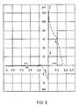
- FIG. 3shows a voltage-current characteristic for write and erase operation of the memory device of the present invention.
- FIG. 4shows the dependence on writing pulse critical amplitude on writing pulse time.
- a floating gate transistormay be considered to be a modified MOSFET transistor with a floating conductive pad embedded in the dielectric that insulates the gate from the source/drain. Because of the very high resistivity of commonly used dielectrics, such as SiO 2 and Si 3 O 4 , any electric charge deposited on the floating gate will remain there during the retention time of the device, which can be years. However, it is difficult to discharge the floating gate simply by applying a reverse external electric field because of the large electrical resistance of the tunnel barrier in the reverse direction. For this reason, the conductivity of the dielectric is typically enhanced by illuminating the dielectric with UV light.
- the present inventionprovides a structure that avoids the need for UV light.
- the present inventionaddress and solves problems related to the control and structure of a floating gate memory device.
- the present inventionprovides for a floating gate memory device that has an insulating layer that acts to either electrically insulate the floating gate from a control gate, or has an increased conductivity to allow for a rapid discharge of the floating gate charge.
- a floating gate transistorhaving an insulating layer between the control gate and the floating gate that comprises a composite material that exhibits structural electronic instability in one dimension and enables static and dynamic control over the conductivity of the composite material.
- a molecular matrixis employed with ionic complexes in the matrix. Under the application of an electric field, the ionic complexes dissociate controllably to change the electrical conductivity of the insulating layer.
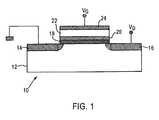
- FIG. 1depicts an exemplary embodiment of the floating gate memory device constructed in accordance with present invention.
- the floating gate memory deviceincludes substrate 12 in which are formed source and drain regions 14 , 16 , respectively.
- a first insulator 18is formed on the substrate 10 and spans the source and drain regions 14 , 16 .
- a floating gate 20formed of conductive material, is formed on the first insulating layer 18 .
- a second insulating layer 22is formed on the floating gate 20 , followed by the formation of gate electrode 24 on the second insulating layer 22 .
- the gate electrode 24 and the drain region 16are depicted as being connected to voltages V g and V d , respectively.
- the gate electrode 24like the floating gate 20 , comprises a conductive material.
- At least one of the two dielectric layers 18 , 22 depicted in FIG. 1comprise a one-dimensional molecular system exhibiting a transition from a low electrical conductivity to a high electrical conductivity and vice versa. This transition is typically manifested by an S-shaped (reentrant) voltage-current characteristic with metastable or stable memory.
- the impedance of such memory cellscan be between ⁇ 10 M ⁇ and ⁇ 100 ⁇ for example, depending on the switching condition. Examples of such molecular systems are systems with a low dimensionality exhibiting a so-called Peierls transition.
- insulating layers 18 , 22A number of different materials may be used as the insulating layers 18 , 22 .Exemplary materials are described in more detail below, but are also discussed in an article by Yu H. Krieger, entitled “ Structural Instability of One - Dimensional Systems as a Physical Principle Underlying the Functioning of Molecular Electronic Devices ”, Journal of Structural Chemistry, Vol. 40, No. 4, 1999 (Yu H. Krieger), expressly incorporated by reference herein.
- Polyconjugated systemsprimarily involve polyvinylenes, i.e., polymers with an acyclic conjugation system, in which the one-dimensional character of structure is dictated by the mechanism of conjugation in linear macromolecules.
- Polyacetyleneis a classical representative of this class of polymers. Its electronic structure is a prototype for many other conjugated polymers.
- molecular compoundsare formed from aromatic and heterocyclic molecules which possess high electric conductivity due to ⁇ -bonds between molecules. Such molecular systems are called ⁇ -complexes or charge transfer complexes, with those systems whose structure involves isolated one-dimensional columns or strands possessing pronounced electro-physical properties of interest for switching and memory applications.
- Molecular charge transfer complexesare donor-acceptor systems formed from two molecules: one possessing donor and another acceptor properties.
- TCNQtetra-cyano-quino-dimethane
- TCNQtetra-cyano-quino-dimethane
- the cationsare dynamically disordered. It involves molecular compounds having the general formula (TMTSF) 2 X. Transition metal salts of K 2 Pt(CN) 4 Br 0.3 ⁇ 3H 2 O(KCP) type are also the typical representatives of mixed-valence quasi-one-dimensional complexes, as are phthalocyanines and porphyrins. Moreover, pure inorganic compounds, such as NbSe 3 , are also interesting examples of compounds with quasi-one-dimensional structure.
- FIGS. 2 a - 2 dAn exemplary molecular composite that can be applied as at least one of the insulating layers 18 , 22 in the floating gate transistor 10 is shown in FIGS. 2 a - 2 d .
- the molecular compositeincludes a quasi-one-dimensional, or at least structurally and electrically anisotropic, molecular matrix, wherein ionic complexes are distributed in the matrix.
- Polyconjugated compoundssuch as the exemplary quasi-one-dimensional systems described above, for example, polyphenylacetylene, can be used as the anisotropic molecular matrix.
- the ionic complexcan be a salt, such as sodium chloride (NaCl), or any other material that can dissociate in an applied electric field.
- NaClsodium chloride
- the exemplary anisotropic molecular matrixis depicted in FIGS. 2 a-d as comprising an assembly of chain-like molecules oriented perpendicular to the electrode surfaces. However, other orientations of those molecules or of anisotropic “channels” are possible as long as a charge separation of the type depicted in FIGS. 2 a-d is enabled.
- Electric switching in the molecular thin films depicted in FIGS. 2 a-dis characterized by the existence of two stable states, a high impedance state (“off” state) and a low impedance state (“on” state).
- the impedance of this “off” stateis usually more than ⁇ 10 M ⁇ ., for example. Switching from the “off” state to the “on” state occurs when an applied electric field exceeds a threshold value.
- the impedance of this “on” statecan be less than ⁇ 100 ⁇ ., for example.
- a transition from “on” state back to the “off” statecan take place by reversing the polarity of the electric field.
- the metastable mode of the memory cell functionis characterized by the low P W and P ER value (0.1-0.5V), high impedance of the “ON” state (wide region, about 1 k ⁇ -1M ⁇ ), short switching time (less than 1 ⁇ s), and short retention time between about 10 s or several hours.
- the stable mode of the memory cell operationshows the high P W and P ER value (3-10V), low impedance of the “ON” state (less than 100 ⁇ ), long switching time (1 ms and more) and long storage time (between several months and years).
- FIG. 2 aillustrates the “off” state, where the electrical conductivity is essentially zero, assuming that the anisotropic molecular matrix itself is a good electrical insulator.
- an external electric field Eis applied, as indicated in FIG. 2 b , the sodium salt dissociates into sodium and chlorine ions, and the ions are displaced from their original position in the anisotropic molecular matrix, resulting in an increase in the electrical conductivity to the metastable “on” state.
- the ionsbecome more strongly separated (FIG. 2 c ), accompanied by a still further increase in the conductivity of the “on” state to the above-described stable state.
- the anions and cationsaccumulate at the electrodes (FIG. 2 d ), resulting in a sharp decrease in the electrical conductivity due to the absence of mobile charges (“off” state).
- the electrode materialcan be, for example, a metal, such as Al or Cu, ITO, a semiconductor or a conducting polymer.
- the transition from the “off” state depicted in FIG. 2 a to the “on” state depicted in FIG. 2 brequires application of an external voltage of approximately 3-5 V for a time period of approximately 10-100 ns.
- the transition from the “off” state depicted in FIG. 2 a to the “on” state depicted in FIG. 2 c having a higher electrical conductivity and longer retention timeis achieved by applying an external voltage of approximately 3-5 V for a time period of approximately 300 ns-1 ⁇ s.
- a molecular compositecomprising polyphenylacetylene and ⁇ 5-7% NaCl as the ionic complex are described in these figures as an exemplary embodiment.
- the current-voltage (I-V) characteristic of a floating gate transistoras it applies to the state of the composite material forming, for example, insulating layer 22 , is shown in FIG. 3 .
- the positive voltage applied to the gate electrode with respect to the groundwill be referred to as write voltage (in pulsed experiments, as write pulse) (P W ), which renders the insulating layer 22 conductive, and the negative voltage, which restores the insulating properties of insulating layer 22 , as erase voltage (or erase pulse) (P ER ), respectively.
- FIG. 3shows a typical I-V curve for write (positive applied voltage) and erase operation (negative applied voltage).
- the deviceis in the “off” state, until the applied voltage reaches a critical value of approximately 0.3 V. In the “off” state, the electric current through the memory cell is essentially zero.
- the applied voltageexceeds the critical voltage of 0.3V, the memory cell 10 approaches zero resistance, with the voltage across the cell dropping to a very small value and the current increasing to more than 120 ⁇ A, with the cell attaining the “on” state.
- the cellremains in the “on” state until a negative voltage is applied, which in the present example is approximately ⁇ 1 V. This represents the erase cycle. After the erase cycle is completed, the cell is again in the “off” state.
- the parameters (voltage, pulse duration) used for the erase operationdepend on the characteristic values of the “on” state of the device.
- the pulse duration of a write pulse required to change the conductivity of the insulating layer 22is related to the amplitude of the write pulse.
- insulating layer 22may be switched from the “off” state to the “on” state by applying a pulse of 4 V for 10 ⁇ s, whereas a pulse duration of more than 1 ms may be required when writing with a voltage of approximately 1 V. Accordingly, the speed with which the conductivity of the insulating layer 22 of the device 10 changes can be adapted to specific applications.
- the present inventionthus provides an easily erasable floating gate transistor memory chip for systems, employing molecular memory cells.
- the electronic circuitry of the erasable floating gate transistor memory chipcan be based on that of well-developed DRAM chips.
- the circuitcan work as either SRAM or DRAM.
Landscapes
- Engineering & Computer Science (AREA)
- Chemical & Material Sciences (AREA)
- Nanotechnology (AREA)
- Physics & Mathematics (AREA)
- Mathematical Physics (AREA)
- Theoretical Computer Science (AREA)
- Crystallography & Structural Chemistry (AREA)
- Semiconductor Memories (AREA)
- Non-Volatile Memory (AREA)
Abstract
Description
Claims (7)
Priority Applications (1)
| Application Number | Priority Date | Filing Date | Title |
|---|---|---|---|
| US10/139,331US6627944B2 (en) | 2001-05-07 | 2002-05-07 | Floating gate memory device using composite molecular material |
Applications Claiming Priority (2)
| Application Number | Priority Date | Filing Date | Title |
|---|---|---|---|
| US28909101P | 2001-05-07 | 2001-05-07 | |
| US10/139,331US6627944B2 (en) | 2001-05-07 | 2002-05-07 | Floating gate memory device using composite molecular material |
Publications (2)
| Publication Number | Publication Date |
|---|---|
| US20020163030A1 US20020163030A1 (en) | 2002-11-07 |
| US6627944B2true US6627944B2 (en) | 2003-09-30 |
Family
ID=23110014
Family Applications (1)
| Application Number | Title | Priority Date | Filing Date |
|---|---|---|---|
| US10/139,331Expired - LifetimeUS6627944B2 (en) | 2001-05-07 | 2002-05-07 | Floating gate memory device using composite molecular material |
Country Status (7)
| Country | Link |
|---|---|
| US (1) | US6627944B2 (en) |
| EP (1) | EP1390984B1 (en) |
| JP (1) | JP4514016B2 (en) |
| KR (1) | KR100885276B1 (en) |
| CN (1) | CN1276518C (en) |
| DE (1) | DE60233486D1 (en) |
| WO (1) | WO2002091476A1 (en) |
Cited By (12)
| Publication number | Priority date | Publication date | Assignee | Title |
|---|---|---|---|---|
| US20020163828A1 (en)* | 2001-05-07 | 2002-11-07 | Coatue Corporation | Memory device with a self-assembled polymer film and method of making the same |
| US20020163830A1 (en)* | 2001-05-07 | 2002-11-07 | Coatue Corporation | Molecular memory device |
| US20030155602A1 (en)* | 2001-08-13 | 2003-08-21 | Coatue Corporation | Memory device |
| US20030178667A1 (en)* | 2001-08-13 | 2003-09-25 | Krieger Juri H. | Memory device |
| US20030234397A1 (en)* | 2002-03-22 | 2003-12-25 | Gunter Schmid | Semiconductor memory cell and semiconductor memory device |
| US20040026714A1 (en)* | 2001-08-13 | 2004-02-12 | Krieger Juri H. | Memory device with active passive layers |
| US20040062070A1 (en)* | 2002-09-27 | 2004-04-01 | Coulson Richard L. | Reducing the effect of write disturbs in polymer memories |
| US20040214351A1 (en)* | 2003-04-23 | 2004-10-28 | Micron Technology, Inc. | Polymer-based ferroelectric memory |
| US6873540B2 (en)* | 2001-05-07 | 2005-03-29 | Advanced Micro Devices, Inc. | Molecular memory cell |
| US7183141B1 (en) | 2001-05-07 | 2007-02-27 | Spansion Llc | Reversible field-programmable electric interconnects |
| US7254053B2 (en)* | 2001-08-13 | 2007-08-07 | Advanced Micro Devices, Inc. | Active programming and operation of a memory device |
| US7460698B2 (en) | 1996-09-25 | 2008-12-02 | Kabushiki Kaisha Toshiba | Ultrasonic picture processing method and ultrasonic picture processing apparatus |
Families Citing this family (20)
| Publication number | Priority date | Publication date | Assignee | Title |
|---|---|---|---|---|
| CN100367528C (en) | 2001-05-07 | 2008-02-06 | 先进微装置公司 | Switching device with memory effect |
| DE60233486D1 (en) | 2001-05-07 | 2009-10-08 | Advanced Micro Devices Inc | FLOATING GATE MEMORY BUILDING PART USING COMPOUND MOLECULAR MATERIAL |
| US6858481B2 (en)* | 2001-08-13 | 2005-02-22 | Advanced Micro Devices, Inc. | Memory device with active and passive layers |
| US7012276B2 (en) | 2002-09-17 | 2006-03-14 | Advanced Micro Devices, Inc. | Organic thin film Zener diodes |
| US6903361B2 (en) | 2003-09-17 | 2005-06-07 | Micron Technology, Inc. | Non-volatile memory structure |
| US6916696B1 (en) | 2003-11-20 | 2005-07-12 | Advanced Micro Devices, Inc. | Method for manufacturing a memory element |
| US20050212022A1 (en)* | 2004-03-24 | 2005-09-29 | Greer Edward C | Memory cell having an electric field programmable storage element, and method of operating same |
| KR100838931B1 (en) | 2004-05-18 | 2008-06-16 | 휴렛-팩커드 디벨롭먼트 컴퍼니, 엘 피 | Material composition that causes electron switching through intramolecular charge transfer, intermolecular charge transfer, or charge transfer between molecules and electrodes induced by an electric field |
| US20050274609A1 (en)* | 2004-05-18 | 2005-12-15 | Yong Chen | Composition of matter which results in electronic switching through intra- or inter- molecular charge transfer, or charge transfer between molecules and electrodes induced by an electrical field |
| DE102004031135A1 (en)* | 2004-06-28 | 2006-01-19 | Infineon Technologies Ag | Resistive semiconductor element based on a solid-state ion conductor |
| US20070009821A1 (en)* | 2005-07-08 | 2007-01-11 | Charlotte Cutler | Devices containing multi-bit data |
| KR100744566B1 (en)* | 2006-09-08 | 2007-08-01 | 한국전자통신연구원 | Gate stack using metal oxide, transistor-integrated memory device including same, and method of driving same |
| US7915603B2 (en)* | 2006-10-27 | 2011-03-29 | Qimonda Ag | Modifiable gate stack memory element |
| KR100890212B1 (en)* | 2007-11-23 | 2009-03-25 | 고려대학교 산학협력단 | Nonvolatile Memory Device and Manufacturing Method Thereof |
| TWI466271B (en)* | 2010-07-05 | 2014-12-21 | Macronix Int Co Ltd | Transistor having an adjustable gate resistance and semiconductor device comprising the same |
| CN102339846B (en)* | 2010-07-19 | 2015-10-07 | 旺宏电子股份有限公司 | Semiconductor memory element having transistor with adjustable gate resistance value |
| US8675381B2 (en) | 2010-07-20 | 2014-03-18 | Macronix International Co., Ltd. | Transistor having an adjustable gate resistance and semiconductor device comprising the same |
| KR101463782B1 (en) | 2011-04-06 | 2014-11-21 | 고려대학교 산학협력단 | Non-volatile memory device using threshold switching material and manufacturing method of the same |
| US9767407B2 (en) | 2015-09-18 | 2017-09-19 | Samsung Electronics Co., Ltd. | Weighting device, neural network, and operating method of the weighting device |
| WO2018009175A1 (en)* | 2016-07-06 | 2018-01-11 | Intel Corporation | High speed single transistor non-volatile memory cell |
Citations (95)
| Publication number | Priority date | Publication date | Assignee | Title |
|---|---|---|---|---|
| US3719933A (en) | 1970-04-02 | 1973-03-06 | Matsushita Electric Industrial Co Ltd | Memory device having lead dioxide particles therein |
| US3810127A (en) | 1970-06-23 | 1974-05-07 | Intel Corp | Programmable circuit {13 {11 the method of programming thereof and the devices so programmed |
| US4267583A (en) | 1978-11-27 | 1981-05-12 | Nippon Electric Co., Ltd. | Memory test device with write and pseudo write signals |
| US4267558A (en)* | 1979-01-05 | 1981-05-12 | Texas Instruments Incorporated | Electrically erasable memory with self-limiting erase |
| US4371883A (en) | 1980-03-14 | 1983-02-01 | The Johns Hopkins University | Current controlled bistable electrical organic thin film switching device |
| US4616340A (en) | 1981-10-14 | 1986-10-07 | Agency Of Industrial Science & Technology | Non-volatile semiconductor memory |
| US4631562A (en) | 1985-05-31 | 1986-12-23 | Rca Corporation | Zener diode structure |
| US4652894A (en) | 1980-03-14 | 1987-03-24 | The Johns Hopkins University | Electrical organic thin film switching device switching between detectably different oxidation states |
| US4677742A (en) | 1983-01-18 | 1987-07-07 | Energy Conversion Devices, Inc. | Electronic matrix arrays and method for making the same |
| US4727514A (en) | 1986-02-11 | 1988-02-23 | Texas Instruments Incorporated | Programmable memory with memory cells programmed by addressing |
| US4733375A (en) | 1984-05-28 | 1988-03-22 | Seiko Epson Corporation | Non-volatile memory circuit |
| EP0268370A2 (en) | 1986-10-13 | 1988-05-25 | Canon Kabushiki Kaisha | Switching device |
| US4834911A (en) | 1986-08-25 | 1989-05-30 | Electro-Organic Company | Intrinsically conductive and semiconductive polymers, products formed with such polymers and methods of forming same |
| US4839700A (en) | 1987-12-16 | 1989-06-13 | California Institute Of Technology | Solid-state non-volatile electronically programmable reversible variable resistance device |
| US4860254A (en) | 1986-01-31 | 1989-08-22 | Bayer Aktiengesellschaft | Non-volatile electronic memory |
| EP0385688A2 (en) | 1989-02-27 | 1990-09-05 | Matsushita Electric Industrial Co., Ltd. | Ferroelectric liquid crystal composition and ferroelectric liquid crystal display device |
| US5012445A (en) | 1987-10-13 | 1991-04-30 | Hitachi, Ltd. | Programmable read only memory being capable of controlling internal writing voltage of external voltage |
| US5034192A (en) | 1984-11-23 | 1991-07-23 | Massachusetts Institute Of Technology | Molecule-based microelectronic devices |
| US5130380A (en) | 1990-05-29 | 1992-07-14 | Carew Evan B | Conductive polymers |
| US5136212A (en) | 1988-02-18 | 1992-08-04 | Canon Kabushiki Kaisha | Electron emitting device, electron generator employing said electron emitting device, and method for driving said generator |
| US5153681A (en)* | 1989-07-25 | 1992-10-06 | Matsushita Electric Industrial Co., Ltd. | Electrcally plastic device and its control method |
| WO1993004506A1 (en) | 1991-08-19 | 1993-03-04 | Energy Conversion Devices, Inc. | Electrically erasable, directly overwritable, multibit single cell memory elements and arrays fabricated therefrom |
| US5196912A (en) | 1988-10-28 | 1993-03-23 | Casio Computer Co., Ltd. | Thin film transistor having memory function and method for using thin film transistor as memory element |
| US5206525A (en)* | 1989-12-27 | 1993-04-27 | Nippon Petrochemicals Co., Ltd. | Electric element capable of controlling the electric conductivity of π-conjugated macromolecular materials |
| US5245543A (en) | 1990-12-21 | 1993-09-14 | Texas Instruments Incorporated | Method and apparatus for integrated circuit design |
| US5296716A (en) | 1991-01-18 | 1994-03-22 | Energy Conversion Devices, Inc. | Electrically erasable, directly overwritable, multibit single cell memory elements and arrays fabricated therefrom |
| US5315131A (en)* | 1990-11-22 | 1994-05-24 | Matsushita Electric Industrial Co., Ltd. | Electrically reprogrammable nonvolatile memory device |
| US5355235A (en) | 1991-08-15 | 1994-10-11 | Kabushiki Kaisha Toshiba | Organic field effect element having organic layers with different carrier concentrations |
| US5392236A (en) | 1992-06-30 | 1995-02-21 | Nec Corporation | Semiconductor memory device |
| JPH07106440A (en) | 1993-10-04 | 1995-04-21 | Hitachi Ltd | Nonvolatile semiconductor memory device and application system using the same |
| US5412614A (en) | 1991-08-16 | 1995-05-02 | U.S. Philips Corporation | Electronic matrix array devices and systems incorporating such devices |
| US5431883A (en)* | 1991-01-24 | 1995-07-11 | Commissariat Energie Atomique | Detector for the detection of chemical species or photons using a field effect transistor |
| US5440518A (en) | 1991-06-12 | 1995-08-08 | Hazani; Emanuel | Non-volatile memory circuits, architecture and methods |
| EP0727822A2 (en) | 1995-02-14 | 1996-08-21 | Canon Kabushiki Kaisha | Semiconductor memory device |
| US5563081A (en) | 1992-03-23 | 1996-10-08 | Rohm Co., Inc. | Method for making a nonvolatile memory device utilizing a field effect transistor having a ferroelectric gate film |
| US5572472A (en) | 1995-04-14 | 1996-11-05 | Delco Electronics Corporation | Integrated zener-zap nonvolatile memory cell with programming and pretest capability |
| US5579199A (en) | 1992-11-26 | 1996-11-26 | Sharp Kabushiki Kaisha | Non-volatile memory device and a method for producing the same |
| RU2071126C1 (en) | 1992-08-27 | 1996-12-27 | Кригер Юрий Генрихович | Storage element |
| US5670818A (en) | 1990-04-12 | 1997-09-23 | Actel Corporation | Electrically programmable antifuse |
| US5691935A (en) | 1995-07-13 | 1997-11-25 | Douglass; Barry G. | Memory element and method of operation thereof |
| US5698874A (en) | 1993-11-02 | 1997-12-16 | Sony Corporation | Photoelectric cell having first and second insulated gates on first and second channel forming regions |
| US5734605A (en) | 1996-09-10 | 1998-03-31 | Motorola, Inc. | Multi-layer magnetic tunneling junction memory cells |
| DE19640239A1 (en) | 1996-09-30 | 1998-04-02 | Siemens Ag | Storage cell with polymer capacitor |
| US5761115A (en) | 1996-05-30 | 1998-06-02 | Axon Technologies Corporation | Programmable metallization cell structure and method of making same |
| US5770885A (en) | 1990-04-12 | 1998-06-23 | Actel Corporation | Electrically programmable antifuse incorporating dielectric and amorphous silicon interlayers |
| US5818749A (en) | 1993-08-20 | 1998-10-06 | Micron Technology, Inc. | Integrated circuit memory device |
| US5849403A (en) | 1995-09-13 | 1998-12-15 | Kabushiki Kaisha Toshiba | Organic thin film device |
| WO1999004440A1 (en) | 1997-07-14 | 1999-01-28 | Technion Research And Development Foundation Ltd. | Microelectronic components and electronic networks comprising dna |
| US5869882A (en) | 1994-09-30 | 1999-02-09 | Texas Instruments Incorporated | Zener diode structure with high reverse breakdown voltage |
| WO1999008325A2 (en) | 1997-07-22 | 1999-02-18 | Thin Film Electronics Asa | Electrode means, with or without functional elements and an electrode device formed of said means |
| WO1999014762A1 (en) | 1997-09-01 | 1999-03-25 | Thin Film Electronics Asa | A read-only memory and read-only memory device |
| WO1999019900A2 (en) | 1997-10-14 | 1999-04-22 | Patterning Technologies Limited | Method of forming an electronic device |
| US5900662A (en) | 1995-11-06 | 1999-05-04 | Sgs Thomson Microelectronics S.R.L. | MOS technology power device with low output resistance and low capacitance, and related manufacturing process |
| US6055180A (en) | 1997-06-17 | 2000-04-25 | Thin Film Electronics Asa | Electrically addressable passive device, method for electrical addressing of the same and uses of the device and the method |
| US6060338A (en) | 1989-01-10 | 2000-05-09 | Mitsubishi Denki Kabushiki Kaisha | Method of making a field effect transistor |
| WO2000026918A1 (en) | 1998-10-30 | 2000-05-11 | Nikolai Schwabe | Magnetic storage device |
| US6064589A (en) | 1998-02-02 | 2000-05-16 | Walker; Darryl G. | Double gate DRAM memory cell |
| US6088319A (en) | 1995-06-23 | 2000-07-11 | Thin Film Electronics Asa | Method for writing of data in an optical memory, apparatus for performing the method and optical memory formed thereby |
| WO2000048196A1 (en) | 1999-02-11 | 2000-08-17 | Arizona Board Of Regents | Programmable microelectronic devices and methods of forming and programming same |
| US6118684A (en) | 1997-10-03 | 2000-09-12 | Yihong; Wu | Optical memories using electron trapping material |
| US6128214A (en) | 1999-03-29 | 2000-10-03 | Hewlett-Packard | Molecular wire crossbar memory |
| US6150705A (en) | 1993-07-07 | 2000-11-21 | Actel Corporation | Dielectric-polysilicon-dielectric-polysilicon-dielectric antifuse for field programmable logic application |
| DE19959904A1 (en) | 1999-12-11 | 2001-06-28 | Edward William Schlag | Regulating electric current through medium, useful as molecular switch in electronics or chemical process control, involves changing parameter inhibiting internal motion of adjacent molecular sections of chain molecule |
| US20010014038A1 (en) | 1998-02-19 | 2001-08-16 | Sanyo Electric Co., Ltd. | Write circuit for a semiconductor memory device |
| US6288697B1 (en) | 1996-11-15 | 2001-09-11 | Sharp Kabushiki Kaisha | Method and circuit for driving display device |
| US6292396B1 (en) | 1999-04-21 | 2001-09-18 | Stmicroelectronics S.A. | Method and device for the programming of an electrically programmable non-volatile memory for improved reliability |
| US20010055384A1 (en) | 2000-03-22 | 2001-12-27 | Shunpei Yamazaki | Electronic device |
| US20010054709A1 (en) | 1999-03-29 | 2001-12-27 | Heath James R. | Chemically synthesized and assembled electronic devices |
| US6349054B1 (en) | 2000-12-25 | 2002-02-19 | Mitsubishi Denki Kabushiki Kaisha | Thin film magnetic memory device including memory cells having a magnetic tunnel junction |
| US20020027819A1 (en) | 1999-02-12 | 2002-03-07 | David Tomanek | Nanocapsules containing charged particles, their uses and methods of forming same |
| WO2002035580A2 (en) | 2000-10-24 | 2002-05-02 | Molecular Electronics Corporation | Three-terminal field-controlled molecular devices |
| US6384427B1 (en) | 1999-10-29 | 2002-05-07 | Semiconductor Energy Laboratory Co., Ltd. | Electronic device |
| WO2002037500A1 (en) | 2000-10-31 | 2002-05-10 | The Regents Of The University Of California | Organic bistable device and organic memory cells |
| WO2002043071A1 (en) | 2000-11-27 | 2002-05-30 | Thin Film Electronics Asa | A ferroelectric memory circuit and method for its fabrication |
| US6403397B1 (en) | 2000-06-28 | 2002-06-11 | Agere Systems Guardian Corp. | Process for fabricating organic semiconductor device involving selective patterning |
| US6403396B1 (en) | 1998-01-28 | 2002-06-11 | Thin Film Electronics Asa | Method for generation of electrically conducting or semiconducting structures in three dimensions and methods for erasure of the same structures |
| US6407953B1 (en) | 2001-02-02 | 2002-06-18 | Matrix Semiconductor, Inc. | Memory array organization and related test method particularly well suited for integrated circuits having write-once memory arrays |
| US6418049B1 (en) | 1997-12-04 | 2002-07-09 | Arizona Board Of Regents | Programmable sub-surface aggregating metallization structure and method of making same |
| US6424553B2 (en) | 2000-03-22 | 2002-07-23 | Thin Film Electronics Asa | Multidimensional addressing architecture for electronic devices |
| US6426891B1 (en) | 1999-10-27 | 2002-07-30 | Sony Corporation | Nonvolatile memory with a two-terminal switching element and its driving method |
| US20020101763A1 (en) | 2001-02-01 | 2002-08-01 | Mitsubishi Denki Kabushiki Kaisha | Non-volatile semiconductor memory device |
| US6429457B1 (en) | 1998-01-16 | 2002-08-06 | Thin Film Electronics Asa | Field-effect transistor |
| US20020104889A1 (en) | 2000-09-25 | 2002-08-08 | Forrest Stephen R. | Smart card composed of organic processing elements |
| US6449184B2 (en) | 2000-06-19 | 2002-09-10 | Matsushita Electric Industrial Co., Ltd. | Method for driving semiconductor memory |
| US20020125504A1 (en) | 2001-03-07 | 2002-09-12 | Perlov Craig M. | Fabrication and assembly structures and methods for memory devices |
| WO2002078003A2 (en) | 2001-03-21 | 2002-10-03 | Matrix Semiconductor, Inc. | Method and apparatus for biasing selected and unselected array lines when writing a memory array |
| US6461916B1 (en) | 1997-03-28 | 2002-10-08 | Hitachi, Ltd. | Non-volatile semiconductor memory and method of making same, and semiconductor device and method of making the device |
| US20020163830A1 (en) | 2001-05-07 | 2002-11-07 | Coatue Corporation | Molecular memory device |
| US20020163831A1 (en) | 2001-05-07 | 2002-11-07 | Coatue Corporation | Molecular memory cell |
| US20020163030A1 (en) | 2001-05-07 | 2002-11-07 | Coatue Corporation | Floating gate memory device using composite molecular material |
| US20020163829A1 (en) | 2001-05-07 | 2002-11-07 | Coatue Corporation | Memory switch |
| US20020163057A1 (en) | 2001-05-07 | 2002-11-07 | Coatue Corporation | Reversible field-programmable electric interconnects |
| US20020163828A1 (en) | 2001-05-07 | 2002-11-07 | Coatue Corporation | Memory device with a self-assembled polymer film and method of making the same |
| US20020168820A1 (en) | 2000-09-08 | 2002-11-14 | Kozicki Michael N. | Microelectronic programmable device and methods of forming and programming the same |
| US6487106B1 (en) | 1999-01-12 | 2002-11-26 | Arizona Board Of Regents | Programmable microelectronic devices and method of forming and programming same |
Family Cites Families (4)
| Publication number | Priority date | Publication date | Assignee | Title |
|---|---|---|---|---|
| JPH02239664A (en)* | 1989-03-13 | 1990-09-21 | Olympus Optical Co Ltd | electrical storage device |
| JP2502782B2 (en)* | 1990-02-15 | 1996-05-29 | 松下電器産業株式会社 | Electroplastic device for neural network and control method thereof |
| JP3273582B2 (en)* | 1994-05-13 | 2002-04-08 | キヤノン株式会社 | Storage device |
| JP2728123B2 (en)* | 1995-07-24 | 1998-03-18 | 日本電気株式会社 | Switching element and manufacturing method thereof |
- 2002
- 2002-05-07DEDE60233486Tpatent/DE60233486D1/ennot_activeExpired - Lifetime
- 2002-05-07WOPCT/US2002/014237patent/WO2002091476A1/enactiveApplication Filing
- 2002-05-07USUS10/139,331patent/US6627944B2/ennot_activeExpired - Lifetime
- 2002-05-07JPJP2002588633Apatent/JP4514016B2/ennot_activeExpired - Fee Related
- 2002-05-07EPEP02769351Apatent/EP1390984B1/ennot_activeExpired - Lifetime
- 2002-05-07KRKR1020037014467Apatent/KR100885276B1/ennot_activeExpired - Fee Related
- 2002-05-07CNCNB02812491XApatent/CN1276518C/ennot_activeExpired - Fee Related
Patent Citations (104)
| Publication number | Priority date | Publication date | Assignee | Title |
|---|---|---|---|---|
| US3719933A (en) | 1970-04-02 | 1973-03-06 | Matsushita Electric Industrial Co Ltd | Memory device having lead dioxide particles therein |
| US3810127A (en) | 1970-06-23 | 1974-05-07 | Intel Corp | Programmable circuit {13 {11 the method of programming thereof and the devices so programmed |
| US4267583A (en) | 1978-11-27 | 1981-05-12 | Nippon Electric Co., Ltd. | Memory test device with write and pseudo write signals |
| US4267558A (en)* | 1979-01-05 | 1981-05-12 | Texas Instruments Incorporated | Electrically erasable memory with self-limiting erase |
| US4371883A (en) | 1980-03-14 | 1983-02-01 | The Johns Hopkins University | Current controlled bistable electrical organic thin film switching device |
| US4652894A (en) | 1980-03-14 | 1987-03-24 | The Johns Hopkins University | Electrical organic thin film switching device switching between detectably different oxidation states |
| US4616340A (en) | 1981-10-14 | 1986-10-07 | Agency Of Industrial Science & Technology | Non-volatile semiconductor memory |
| US4677742A (en) | 1983-01-18 | 1987-07-07 | Energy Conversion Devices, Inc. | Electronic matrix arrays and method for making the same |
| USRE34974E (en) | 1984-05-28 | 1995-06-20 | Seiko Epson Corporation | Non-volatile memory circuit |
| US4733375A (en) | 1984-05-28 | 1988-03-22 | Seiko Epson Corporation | Non-volatile memory circuit |
| US5034192A (en) | 1984-11-23 | 1991-07-23 | Massachusetts Institute Of Technology | Molecule-based microelectronic devices |
| US4631562A (en) | 1985-05-31 | 1986-12-23 | Rca Corporation | Zener diode structure |
| US4860254A (en) | 1986-01-31 | 1989-08-22 | Bayer Aktiengesellschaft | Non-volatile electronic memory |
| US4727514A (en) | 1986-02-11 | 1988-02-23 | Texas Instruments Incorporated | Programmable memory with memory cells programmed by addressing |
| US4834911A (en) | 1986-08-25 | 1989-05-30 | Electro-Organic Company | Intrinsically conductive and semiconductive polymers, products formed with such polymers and methods of forming same |
| EP0268370A2 (en) | 1986-10-13 | 1988-05-25 | Canon Kabushiki Kaisha | Switching device |
| US5012445A (en) | 1987-10-13 | 1991-04-30 | Hitachi, Ltd. | Programmable read only memory being capable of controlling internal writing voltage of external voltage |
| US4839700A (en) | 1987-12-16 | 1989-06-13 | California Institute Of Technology | Solid-state non-volatile electronically programmable reversible variable resistance device |
| US5136212A (en) | 1988-02-18 | 1992-08-04 | Canon Kabushiki Kaisha | Electron emitting device, electron generator employing said electron emitting device, and method for driving said generator |
| US5196912A (en) | 1988-10-28 | 1993-03-23 | Casio Computer Co., Ltd. | Thin film transistor having memory function and method for using thin film transistor as memory element |
| US6060338A (en) | 1989-01-10 | 2000-05-09 | Mitsubishi Denki Kabushiki Kaisha | Method of making a field effect transistor |
| EP0385688A2 (en) | 1989-02-27 | 1990-09-05 | Matsushita Electric Industrial Co., Ltd. | Ferroelectric liquid crystal composition and ferroelectric liquid crystal display device |
| US5153681A (en)* | 1989-07-25 | 1992-10-06 | Matsushita Electric Industrial Co., Ltd. | Electrcally plastic device and its control method |
| US5206525A (en)* | 1989-12-27 | 1993-04-27 | Nippon Petrochemicals Co., Ltd. | Electric element capable of controlling the electric conductivity of π-conjugated macromolecular materials |
| US5670818A (en) | 1990-04-12 | 1997-09-23 | Actel Corporation | Electrically programmable antifuse |
| US5770885A (en) | 1990-04-12 | 1998-06-23 | Actel Corporation | Electrically programmable antifuse incorporating dielectric and amorphous silicon interlayers |
| US5130380A (en) | 1990-05-29 | 1992-07-14 | Carew Evan B | Conductive polymers |
| US5315131A (en)* | 1990-11-22 | 1994-05-24 | Matsushita Electric Industrial Co., Ltd. | Electrically reprogrammable nonvolatile memory device |
| US5319564A (en) | 1990-12-21 | 1994-06-07 | Texas Instruments Incorporated | Method and apparatus for integrated circuit design |
| US5245543A (en) | 1990-12-21 | 1993-09-14 | Texas Instruments Incorporated | Method and apparatus for integrated circuit design |
| US5296716A (en) | 1991-01-18 | 1994-03-22 | Energy Conversion Devices, Inc. | Electrically erasable, directly overwritable, multibit single cell memory elements and arrays fabricated therefrom |
| US5431883A (en)* | 1991-01-24 | 1995-07-11 | Commissariat Energie Atomique | Detector for the detection of chemical species or photons using a field effect transistor |
| US5440518A (en) | 1991-06-12 | 1995-08-08 | Hazani; Emanuel | Non-volatile memory circuits, architecture and methods |
| US5355235A (en) | 1991-08-15 | 1994-10-11 | Kabushiki Kaisha Toshiba | Organic field effect element having organic layers with different carrier concentrations |
| US5412614A (en) | 1991-08-16 | 1995-05-02 | U.S. Philips Corporation | Electronic matrix array devices and systems incorporating such devices |
| WO1993004506A1 (en) | 1991-08-19 | 1993-03-04 | Energy Conversion Devices, Inc. | Electrically erasable, directly overwritable, multibit single cell memory elements and arrays fabricated therefrom |
| US5563081A (en) | 1992-03-23 | 1996-10-08 | Rohm Co., Inc. | Method for making a nonvolatile memory device utilizing a field effect transistor having a ferroelectric gate film |
| US5392236A (en) | 1992-06-30 | 1995-02-21 | Nec Corporation | Semiconductor memory device |
| RU2071126C1 (en) | 1992-08-27 | 1996-12-27 | Кригер Юрий Генрихович | Storage element |
| US5579199A (en) | 1992-11-26 | 1996-11-26 | Sharp Kabushiki Kaisha | Non-volatile memory device and a method for producing the same |
| US6150705A (en) | 1993-07-07 | 2000-11-21 | Actel Corporation | Dielectric-polysilicon-dielectric-polysilicon-dielectric antifuse for field programmable logic application |
| US5818749A (en) | 1993-08-20 | 1998-10-06 | Micron Technology, Inc. | Integrated circuit memory device |
| JPH07106440A (en) | 1993-10-04 | 1995-04-21 | Hitachi Ltd | Nonvolatile semiconductor memory device and application system using the same |
| US5698874A (en) | 1993-11-02 | 1997-12-16 | Sony Corporation | Photoelectric cell having first and second insulated gates on first and second channel forming regions |
| US5869882A (en) | 1994-09-30 | 1999-02-09 | Texas Instruments Incorporated | Zener diode structure with high reverse breakdown voltage |
| EP0727822A2 (en) | 1995-02-14 | 1996-08-21 | Canon Kabushiki Kaisha | Semiconductor memory device |
| US5572472A (en) | 1995-04-14 | 1996-11-05 | Delco Electronics Corporation | Integrated zener-zap nonvolatile memory cell with programming and pretest capability |
| US6088319A (en) | 1995-06-23 | 2000-07-11 | Thin Film Electronics Asa | Method for writing of data in an optical memory, apparatus for performing the method and optical memory formed thereby |
| US5691935A (en) | 1995-07-13 | 1997-11-25 | Douglass; Barry G. | Memory element and method of operation thereof |
| US5849403A (en) | 1995-09-13 | 1998-12-15 | Kabushiki Kaisha Toshiba | Organic thin film device |
| US5900662A (en) | 1995-11-06 | 1999-05-04 | Sgs Thomson Microelectronics S.R.L. | MOS technology power device with low output resistance and low capacitance, and related manufacturing process |
| US5896312A (en) | 1996-05-30 | 1999-04-20 | Axon Technologies Corporation | Programmable metallization cell structure and method of making same |
| US5761115A (en) | 1996-05-30 | 1998-06-02 | Axon Technologies Corporation | Programmable metallization cell structure and method of making same |
| US5914893A (en) | 1996-05-30 | 1999-06-22 | Axon Technologies Corporation | Programmable metallization cell structure and method of making same |
| US5734605A (en) | 1996-09-10 | 1998-03-31 | Motorola, Inc. | Multi-layer magnetic tunneling junction memory cells |
| DE19640239A1 (en) | 1996-09-30 | 1998-04-02 | Siemens Ag | Storage cell with polymer capacitor |
| US6288697B1 (en) | 1996-11-15 | 2001-09-11 | Sharp Kabushiki Kaisha | Method and circuit for driving display device |
| US6461916B1 (en) | 1997-03-28 | 2002-10-08 | Hitachi, Ltd. | Non-volatile semiconductor memory and method of making same, and semiconductor device and method of making the device |
| US6055180A (en) | 1997-06-17 | 2000-04-25 | Thin Film Electronics Asa | Electrically addressable passive device, method for electrical addressing of the same and uses of the device and the method |
| WO1999004440A1 (en) | 1997-07-14 | 1999-01-28 | Technion Research And Development Foundation Ltd. | Microelectronic components and electronic networks comprising dna |
| WO1999008325A2 (en) | 1997-07-22 | 1999-02-18 | Thin Film Electronics Asa | Electrode means, with or without functional elements and an electrode device formed of said means |
| US6326936B1 (en) | 1997-07-22 | 2001-12-04 | Thin Film Electronics Asa | Electrode means, comprising polymer materials, with or without functional elements and an electrode device formed of said means |
| WO1999014762A1 (en) | 1997-09-01 | 1999-03-25 | Thin Film Electronics Asa | A read-only memory and read-only memory device |
| US6118684A (en) | 1997-10-03 | 2000-09-12 | Yihong; Wu | Optical memories using electron trapping material |
| WO1999019900A2 (en) | 1997-10-14 | 1999-04-22 | Patterning Technologies Limited | Method of forming an electronic device |
| US6418049B1 (en) | 1997-12-04 | 2002-07-09 | Arizona Board Of Regents | Programmable sub-surface aggregating metallization structure and method of making same |
| US6429457B1 (en) | 1998-01-16 | 2002-08-06 | Thin Film Electronics Asa | Field-effect transistor |
| US6403396B1 (en) | 1998-01-28 | 2002-06-11 | Thin Film Electronics Asa | Method for generation of electrically conducting or semiconducting structures in three dimensions and methods for erasure of the same structures |
| US6432739B1 (en) | 1998-01-28 | 2002-08-13 | Thin Film Electronics Asa | Method for generating electrical conducting or semiconducting structures in two or three dimensions, a method for erasing the same structures and an electric field generator/modulator for use with the method for generating |
| US6064589A (en) | 1998-02-02 | 2000-05-16 | Walker; Darryl G. | Double gate DRAM memory cell |
| US6353559B2 (en) | 1998-02-19 | 2002-03-05 | Sanyo Electric Co., Ltd. | Write circuit for a semiconductor memory device |
| US20010014038A1 (en) | 1998-02-19 | 2001-08-16 | Sanyo Electric Co., Ltd. | Write circuit for a semiconductor memory device |
| WO2000026918A1 (en) | 1998-10-30 | 2000-05-11 | Nikolai Schwabe | Magnetic storage device |
| US6487106B1 (en) | 1999-01-12 | 2002-11-26 | Arizona Board Of Regents | Programmable microelectronic devices and method of forming and programming same |
| WO2000048196A1 (en) | 1999-02-11 | 2000-08-17 | Arizona Board Of Regents | Programmable microelectronic devices and methods of forming and programming same |
| US20020027819A1 (en) | 1999-02-12 | 2002-03-07 | David Tomanek | Nanocapsules containing charged particles, their uses and methods of forming same |
| US20010054709A1 (en) | 1999-03-29 | 2001-12-27 | Heath James R. | Chemically synthesized and assembled electronic devices |
| US6459095B1 (en) | 1999-03-29 | 2002-10-01 | Hewlett-Packard Company | Chemically synthesized and assembled electronics devices |
| US6128214A (en) | 1999-03-29 | 2000-10-03 | Hewlett-Packard | Molecular wire crossbar memory |
| US6292396B1 (en) | 1999-04-21 | 2001-09-18 | Stmicroelectronics S.A. | Method and device for the programming of an electrically programmable non-volatile memory for improved reliability |
| US6426891B1 (en) | 1999-10-27 | 2002-07-30 | Sony Corporation | Nonvolatile memory with a two-terminal switching element and its driving method |
| US6384427B1 (en) | 1999-10-29 | 2002-05-07 | Semiconductor Energy Laboratory Co., Ltd. | Electronic device |
| US20020134979A1 (en) | 1999-10-29 | 2002-09-26 | Semiconductor Energy Laboratory Co., Ltd. | Electronic device |
| DE19959904A1 (en) | 1999-12-11 | 2001-06-28 | Edward William Schlag | Regulating electric current through medium, useful as molecular switch in electronics or chemical process control, involves changing parameter inhibiting internal motion of adjacent molecular sections of chain molecule |
| US20010055384A1 (en) | 2000-03-22 | 2001-12-27 | Shunpei Yamazaki | Electronic device |
| US6424553B2 (en) | 2000-03-22 | 2002-07-23 | Thin Film Electronics Asa | Multidimensional addressing architecture for electronic devices |
| US6449184B2 (en) | 2000-06-19 | 2002-09-10 | Matsushita Electric Industrial Co., Ltd. | Method for driving semiconductor memory |
| US6403397B1 (en) | 2000-06-28 | 2002-06-11 | Agere Systems Guardian Corp. | Process for fabricating organic semiconductor device involving selective patterning |
| US20020168820A1 (en) | 2000-09-08 | 2002-11-14 | Kozicki Michael N. | Microelectronic programmable device and methods of forming and programming the same |
| US20020104889A1 (en) | 2000-09-25 | 2002-08-08 | Forrest Stephen R. | Smart card composed of organic processing elements |
| WO2002035580A2 (en) | 2000-10-24 | 2002-05-02 | Molecular Electronics Corporation | Three-terminal field-controlled molecular devices |
| WO2002037500A1 (en) | 2000-10-31 | 2002-05-10 | The Regents Of The University Of California | Organic bistable device and organic memory cells |
| WO2002043071A1 (en) | 2000-11-27 | 2002-05-30 | Thin Film Electronics Asa | A ferroelectric memory circuit and method for its fabrication |
| US6349054B1 (en) | 2000-12-25 | 2002-02-19 | Mitsubishi Denki Kabushiki Kaisha | Thin film magnetic memory device including memory cells having a magnetic tunnel junction |
| US20020101763A1 (en) | 2001-02-01 | 2002-08-01 | Mitsubishi Denki Kabushiki Kaisha | Non-volatile semiconductor memory device |
| US6407953B1 (en) | 2001-02-02 | 2002-06-18 | Matrix Semiconductor, Inc. | Memory array organization and related test method particularly well suited for integrated circuits having write-once memory arrays |
| US20020125504A1 (en) | 2001-03-07 | 2002-09-12 | Perlov Craig M. | Fabrication and assembly structures and methods for memory devices |
| WO2002078003A2 (en) | 2001-03-21 | 2002-10-03 | Matrix Semiconductor, Inc. | Method and apparatus for biasing selected and unselected array lines when writing a memory array |
| US20020163830A1 (en) | 2001-05-07 | 2002-11-07 | Coatue Corporation | Molecular memory device |
| US20020163831A1 (en) | 2001-05-07 | 2002-11-07 | Coatue Corporation | Molecular memory cell |
| US20020163030A1 (en) | 2001-05-07 | 2002-11-07 | Coatue Corporation | Floating gate memory device using composite molecular material |
| US20020163829A1 (en) | 2001-05-07 | 2002-11-07 | Coatue Corporation | Memory switch |
| US20020163057A1 (en) | 2001-05-07 | 2002-11-07 | Coatue Corporation | Reversible field-programmable electric interconnects |
| US20020163828A1 (en) | 2001-05-07 | 2002-11-07 | Coatue Corporation | Memory device with a self-assembled polymer film and method of making the same |
Non-Patent Citations (38)
| Title |
|---|
| "A Disrupted Organic Film: Could Memories Be Made of This?," ORNL Review, vol. 33, No. 2, 2000. |
| "Technical Summary of Programmable Metallization Cell Memory Technology," Version 1.3, Dec. 2001. |
| "The 1998 Conference Archive," The Sixth Foresight Conference on Molecular Nanotechnology, Nov. 12-15, 1998, www.foresight.org/Conferences/MNT6/index.html. |
| Beck, A. et al., "Reproducible Switching Effect in Thin Oxide Films for Memory Applications," Applied Physics Letters, vol. 77, No. 1, pp. 139-141, Jul. 3, 2000. |
| Bernard, Allen, "A Big Name in Chips Helps Coatue in Molecular Memory Race," Aug. 27, 2000, www.nanoelectronicsplanet.com/features/article/0,4028,6571-1452831,00.html. |
| Chen, J. et al., "Room-temperature Negative Differential Resistance in Nanoscale Molecular Junctions," Applied Physics Letters, vol. 77, No. 8, Aug. 21, 2000. |
| Collier, C. P. et al., "Electrically Configurable Molecular-Based Logic Gates," Science, vol. 285, pp. 391-394, Jul. 16, 1999. |
| Gannon, Andrew, "Toward the Next Generation CD," Physical Review Focus, Feb. 16, 2000. |
| Gao, H. .J. et al., "Reversible Nanometer-Scale Conductance Transitions in an Organic Complex," Physical Review Letters, vol. 84, pp. 1780-1783, Feb. 21, 2000. |
| Gao, H. .J. et al., "Using a New Kind of Organic Complex System of Electrical Bistability for Ultrahigh Density Data Storage," J. Vac. Sci. Technol. B vol. 15, No.4, pp. 1581-1583, Jul./Aug. 1997. |
| International Search Report, PCT/RU01/00334, search completed Feb. 14, 2002. |
| International Search Report, PCT/US02/14237, search completed Sep. 9, 2002. |
| International Search Report, PCT/US02/14238, search completed Aug. 9, 2002. |
| International Search Report, PCT/US02/14239, search completed Aug. 20, 2002. |
| International Search Report, PCT/US02/14269, search completed Mar. 27, 2003. |
| International Search Report, PCT/US02/14270, search completed Mar. 28, 2003. |
| International Search Report, PCTUS02/14236, search completed Aug. 14, 2002. |
| Japanese patent abstract of publication No. 01-103137, Apr. 20, 1989. |
| Japanese patent abstract of publication No. 01278781, Nov. 9, 1989. |
| Japanese patent abstract of publication No. 61107723, May 26, 1986. |
| Japanese patent abstract of publication No. 63293729, Nov. 30, 1998. |
| Krieger, Ju. H. et al., "Molecular Analogue Memory Cell Based on Electrical Switching and Memory in Molecular Thin Films," Synthetic Metals, 7730 (2000), pp. 1-4. |
| Krieger, Juri H. et al., "Molecular Analogue Memory Cell," Sixth Foresight Conference on Molecular Nanotechnology, Santa Clara, California, Nov. 12-15, 1998. |
| Krieger, Yu. G. et al., "Study of Test Structures of a Molecular Memory Element," Institute of Inorganic Chemistry, Siberian Branch, Russian Academy of Sciences. Translated from Zhurmal Strukturnoi Khimii, vol. 34,No. 6, pp. 152-156, Nov.-Dec. 1993. Original article submitted Apr. 27, 1993. |
| Krieger, Yu. G., "Molecular Electronics: Current State and Future Trends," Journal of Structural Chemistry, vol. 34, No. 6, pp. 896-904, Nov.-Dec. 1993. |
| Krieger, Yu. H., "Structural Instability of One-Dimensional Systems as a Physical Principle Underlying the Functioning of Molecular Electronic Devices," Journal of Structural Chemistry, vol. 40, No. 4, pp. 594-619, Jul.-Aug. 1999. |
| Kurita, Ryo et al., "Field Modulation Effects on Charge-Density-Wave Conduction in NbSe3," Physica B, 284-288 (2000), pp. 1161-1662. |
| Ma, L. P. et al., "Data Storage With 0.7 nm Recording Marks on a Crystalline Organic Thin Film by a Scanning Tunneling Microscope," Applied Physics Letters, vol. 73, No. 6, pp. 850-852, Aug. 10, 1998. |
| Ma. L.P. et al., "Nanometer-Scale Recording on an Organic Complex Thin Film With Scanning Tunneling Microscope," Applied Physics Letters, vol. 69, No. 24, pp. 3752-3753, Dec. 9, 1996. |
| Machida, Yasuhiko et al., "Electrical Switching in Evaporated Lead Phthalocyanine Films," Japanese Journal of Applied Physics, vol. 28, No. 2, pp. 297-298, Feb. 1989. |
| Ovshinsky, Stanford R., "Localized States in the Gap of Amorphous Semiconductors," Physical Review Letters, vol. 36, No. 24, pp. 1469-1472, Jun. 14, 1976. |
| Potember, R. S. et al., "Electrical Switching and Memory Phenomena in Cu-TCNQ Thin Films," Applied Physics Letters, vol. 34, No. 6, pp. 405-407, Mar. 15, 1979. |
| Reed, M.A. et al., "Molecular Random Access Memory Cell," Applied Physics Letters, vol. 78, No. 23, pp. 3735-3737, Jun. 4, 2001. |
| Rossel, C. et al., "Electrical Current Distribution Across a Metal-Insulator-Metal Structure During Bistable Switching," Apr. 24, 2001. |
| Rotman, David, "Molecular Memory," Technology Review, May 2001. |
| Semiconductor Times, pp. 5-6, Jul. 2002. |
| Stikeman, Alexandra, "Polymer Memory: The Plastic Path to Better Data Storage," Technology Review, p. 31, Sep. 2002. |
| Zhou, C. et al., "Nanoscale Metal/Self-Assembled Monolayer/Metal Heterostructures," Applied Physics Letters, vol. 71, No. 5, pp. 611-613, Aug. 4, 1997. |
Cited By (25)
| Publication number | Priority date | Publication date | Assignee | Title |
|---|---|---|---|---|
| US7460698B2 (en) | 1996-09-25 | 2008-12-02 | Kabushiki Kaisha Toshiba | Ultrasonic picture processing method and ultrasonic picture processing apparatus |
| US6781868B2 (en)* | 2001-05-07 | 2004-08-24 | Advanced Micro Devices, Inc. | Molecular memory device |
| US20020163830A1 (en)* | 2001-05-07 | 2002-11-07 | Coatue Corporation | Molecular memory device |
| US7183141B1 (en) | 2001-05-07 | 2007-02-27 | Spansion Llc | Reversible field-programmable electric interconnects |
| US6873540B2 (en)* | 2001-05-07 | 2005-03-29 | Advanced Micro Devices, Inc. | Molecular memory cell |
| US6855977B2 (en)* | 2001-05-07 | 2005-02-15 | Advanced Micro Devices, Inc. | Memory device with a self-assembled polymer film and method of making the same |
| US20020163828A1 (en)* | 2001-05-07 | 2002-11-07 | Coatue Corporation | Memory device with a self-assembled polymer film and method of making the same |
| US6838720B2 (en)* | 2001-08-13 | 2005-01-04 | Advanced Micro Devices, Inc. | Memory device with active passive layers |
| US7254053B2 (en)* | 2001-08-13 | 2007-08-07 | Advanced Micro Devices, Inc. | Active programming and operation of a memory device |
| US20030155602A1 (en)* | 2001-08-13 | 2003-08-21 | Coatue Corporation | Memory device |
| US6806526B2 (en)* | 2001-08-13 | 2004-10-19 | Advanced Micro Devices, Inc. | Memory device |
| US6768157B2 (en)* | 2001-08-13 | 2004-07-27 | Advanced Micro Devices, Inc. | Memory device |
| US20040026729A9 (en)* | 2001-08-13 | 2004-02-12 | Coatue Corporation | Memory device |
| US20040026714A1 (en)* | 2001-08-13 | 2004-02-12 | Krieger Juri H. | Memory device with active passive layers |
| US20030178667A1 (en)* | 2001-08-13 | 2003-09-25 | Krieger Juri H. | Memory device |
| US7049628B2 (en)* | 2002-03-22 | 2006-05-23 | Infineon Technologies Ag | Semiconductor memory cell and semiconductor memory device |
| US20030234397A1 (en)* | 2002-03-22 | 2003-12-25 | Gunter Schmid | Semiconductor memory cell and semiconductor memory device |
| US6922350B2 (en)* | 2002-09-27 | 2005-07-26 | Intel Corporation | Reducing the effect of write disturbs in polymer memories |
| US20040062070A1 (en)* | 2002-09-27 | 2004-04-01 | Coulson Richard L. | Reducing the effect of write disturbs in polymer memories |
| US20060003472A1 (en)* | 2003-04-23 | 2006-01-05 | Micron Technology, Inc. | Polymer-based ferroelectric memory |
| US7049153B2 (en) | 2003-04-23 | 2006-05-23 | Micron Technology, Inc. | Polymer-based ferroelectric memory |
| US20040214351A1 (en)* | 2003-04-23 | 2004-10-28 | Micron Technology, Inc. | Polymer-based ferroelectric memory |
| US7768049B2 (en) | 2003-04-23 | 2010-08-03 | Micron Technology, Inc. | Polymer-based ferroelectric memory |
| US20100290265A1 (en)* | 2003-04-23 | 2010-11-18 | Agarwal Vishnu K | Polymer-based ferroelectric memory |
| US8120083B2 (en) | 2003-04-23 | 2012-02-21 | Micron Technology, Inc. | Polymer-based ferroelectric memory |
Also Published As
| Publication number | Publication date |
|---|---|
| DE60233486D1 (en) | 2009-10-08 |
| WO2002091476A1 (en) | 2002-11-14 |
| JP2005501398A (en) | 2005-01-13 |
| KR20030092132A (en) | 2003-12-03 |
| JP4514016B2 (en) | 2010-07-28 |
| KR100885276B1 (en) | 2009-02-23 |
| CN1276518C (en) | 2006-09-20 |
| CN1518775A (en) | 2004-08-04 |
| US20020163030A1 (en) | 2002-11-07 |
| EP1390984B1 (en) | 2009-08-26 |
| EP1390984A1 (en) | 2004-02-25 |
Similar Documents
| Publication | Publication Date | Title |
|---|---|---|
| US6627944B2 (en) | Floating gate memory device using composite molecular material | |
| US6781868B2 (en) | Molecular memory device | |
| US6809955B2 (en) | Addressable and electrically reversible memory switch | |
| US7113420B2 (en) | Molecular memory cell | |
| US6844608B2 (en) | Reversible field-programmable electric interconnects | |
| US7145824B2 (en) | Temperature compensation of thin film diode voltage threshold in memory sensing circuit | |
| KR100276850B1 (en) | Ferroelectric memory transistor with resistively coupled floating gate | |
| US7336520B2 (en) | Storage device and semiconductor apparatus | |
| US7199394B2 (en) | Polymer memory device with variable period of retention time | |
| WO2006124235A1 (en) | Resistive memory device with improved data retention and reduced power | |
| US7035140B2 (en) | Organic-polymer memory element | |
| US8089110B1 (en) | Switchable memory diodes based on ferroelectric/conjugated polymer heterostructures and/or their composites | |
| KR100593607B1 (en) | Nonvolatile semiconductor memory device including ferroelectric semiconductor material and data writing, erasing and reading method of semiconductor memory device |
Legal Events
| Date | Code | Title | Description |
|---|---|---|---|
| AS | Assignment | Owner name:COATUE CORPORATION, MASSACHUSETTS Free format text:ASSIGNMENT OF ASSIGNORS INTEREST;ASSIGNORS:MANDELL, AARON;PERLMAN, ANDREW;REEL/FRAME:012887/0996 Effective date:20020506 | |
| AS | Assignment | Owner name:ADVANCED MICRO DEVICES, INC., CALIFORNIA Free format text:ASSIGNMENT OF ASSIGNORS INTEREST;ASSIGNOR:COATUE CORPORATION;REEL/FRAME:014265/0481 Effective date:20030708 | |
| STCF | Information on status: patent grant | Free format text:PATENTED CASE | |
| FPAY | Fee payment | Year of fee payment:4 | |
| AS | Assignment | Owner name:GLOBALFOUNDRIES INC., CAYMAN ISLANDS Free format text:ASSIGNMENT OF ASSIGNORS INTEREST;ASSIGNOR:AMD TECHNOLOGIES HOLDINGS, INC.;REEL/FRAME:022764/0544 Effective date:20090302 Owner name:AMD TECHNOLOGIES HOLDINGS, INC., CALIFORNIA Free format text:ASSIGNMENT OF ASSIGNORS INTEREST;ASSIGNOR:ADVANCED MICRO DEVICES, INC.;REEL/FRAME:022764/0488 Effective date:20090302 | |
| FPAY | Fee payment | Year of fee payment:8 | |
| REMI | Maintenance fee reminder mailed | ||
| FPAY | Fee payment | Year of fee payment:12 | |
| SULP | Surcharge for late payment | Year of fee payment:11 | |
| AS | Assignment | Owner name:CYPRESS SEMICONDUCTOR CORPORATION, CALIFORNIA Free format text:PARTIAL RELEASE OF SECURITY INTEREST IN PATENTS;ASSIGNOR:MORGAN STANLEY SENIOR FUNDING, INC., AS COLLATERAL AGENT;REEL/FRAME:039708/0001 Effective date:20160811 Owner name:SPANSION LLC, CALIFORNIA Free format text:PARTIAL RELEASE OF SECURITY INTEREST IN PATENTS;ASSIGNOR:MORGAN STANLEY SENIOR FUNDING, INC., AS COLLATERAL AGENT;REEL/FRAME:039708/0001 Effective date:20160811 | |
| AS | Assignment | Owner name:WILMINGTON TRUST, NATIONAL ASSOCIATION, DELAWARE Free format text:SECURITY AGREEMENT;ASSIGNOR:GLOBALFOUNDRIES INC.;REEL/FRAME:049490/0001 Effective date:20181127 | |
| AS | Assignment | Owner name:GLOBALFOUNDRIES INC., CAYMAN ISLANDS Free format text:RELEASE BY SECURED PARTY;ASSIGNOR:WILMINGTON TRUST, NATIONAL ASSOCIATION;REEL/FRAME:054636/0001 Effective date:20201117 | |
| AS | Assignment | Owner name:GLOBALFOUNDRIES U.S. INC., NEW YORK Free format text:RELEASE BY SECURED PARTY;ASSIGNOR:WILMINGTON TRUST, NATIONAL ASSOCIATION;REEL/FRAME:056987/0001 Effective date:20201117 |