US6627547B2 - Hot metallization process - Google Patents
Hot metallization processDownload PDFInfo
- Publication number
- US6627547B2 US6627547B2US09/866,957US86695701AUS6627547B2US 6627547 B2US6627547 B2US 6627547B2US 86695701 AUS86695701 AUS 86695701AUS 6627547 B2US6627547 B2US 6627547B2
- Authority
- US
- United States
- Prior art keywords
- metal
- substrate
- gas
- flow rate
- equal
- Prior art date
- Legal status (The legal status is an assumption and is not a legal conclusion. Google has not performed a legal analysis and makes no representation as to the accuracy of the status listed.)
- Expired - Lifetime, expires
Links
Images


Classifications
- H—ELECTRICITY
- H01—ELECTRIC ELEMENTS
- H01L—SEMICONDUCTOR DEVICES NOT COVERED BY CLASS H10
- H01L21/00—Processes or apparatus adapted for the manufacture or treatment of semiconductor or solid state devices or of parts thereof
- H01L21/70—Manufacture or treatment of devices consisting of a plurality of solid state components formed in or on a common substrate or of parts thereof; Manufacture of integrated circuit devices or of parts thereof
- H01L21/71—Manufacture of specific parts of devices defined in group H01L21/70
- H01L21/768—Applying interconnections to be used for carrying current between separate components within a device comprising conductors and dielectrics
- H01L21/76838—Applying interconnections to be used for carrying current between separate components within a device comprising conductors and dielectrics characterised by the formation and the after-treatment of the conductors
- H01L21/76877—Filling of holes, grooves or trenches, e.g. vias, with conductive material
- H—ELECTRICITY
- H01—ELECTRIC ELEMENTS
- H01L—SEMICONDUCTOR DEVICES NOT COVERED BY CLASS H10
- H01L21/00—Processes or apparatus adapted for the manufacture or treatment of semiconductor or solid state devices or of parts thereof
- H01L21/02—Manufacture or treatment of semiconductor devices or of parts thereof
- H01L21/04—Manufacture or treatment of semiconductor devices or of parts thereof the devices having potential barriers, e.g. a PN junction, depletion layer or carrier concentration layer
- H01L21/18—Manufacture or treatment of semiconductor devices or of parts thereof the devices having potential barriers, e.g. a PN junction, depletion layer or carrier concentration layer the devices having semiconductor bodies comprising elements of Group IV of the Periodic Table or AIIIBV compounds with or without impurities, e.g. doping materials
- H01L21/28—Manufacture of electrodes on semiconductor bodies using processes or apparatus not provided for in groups H01L21/20 - H01L21/268
- H01L21/283—Deposition of conductive or insulating materials for electrodes conducting electric current
- H01L21/285—Deposition of conductive or insulating materials for electrodes conducting electric current from a gas or vapour, e.g. condensation
- H01L21/28506—Deposition of conductive or insulating materials for electrodes conducting electric current from a gas or vapour, e.g. condensation of conductive layers
- H01L21/28512—Deposition of conductive or insulating materials for electrodes conducting electric current from a gas or vapour, e.g. condensation of conductive layers on semiconductor bodies comprising elements of Group IV of the Periodic Table
- H01L21/2855—Deposition of conductive or insulating materials for electrodes conducting electric current from a gas or vapour, e.g. condensation of conductive layers on semiconductor bodies comprising elements of Group IV of the Periodic Table by physical means, e.g. sputtering, evaporation
Definitions
- This inventionrelates to metallization processes for use in making devices such as semiconductor devices, and to devices formed using those metallization processes.
- Formation of a metal layeris a common step in the formation of some devices, such as, for example, semiconductor devices.
- a metal layercan be formed so as to fill in vias or cover steps formed during fabrication of a semiconductor device.
- the formation of a metal layer over vias having a high aspect ratio (i.e., ratio of the depth of the via to the width or diameter of the via) or steps having a relatively large heighthas been subject to several problems, such as cusping and voiding.
- the metal layeris formed using a two step process.
- a relatively thick portion of the metal layeris deposited while the semiconductor wafer is held at a relatively cold temperature (i.e., preferably less than or equal to 200° C. ).
- the thickness of this portionmust be adequate, in view of relevant process parameters (e.g., the geometry being metallized and the metal being used), to ensure that adequate metal is present to avoid the formation of voids during the metal reflow that occurs during the second step.
- this thick portionpreferably has a thickness equal to about 50% to 75% of the total thickness of the metal layer to be formed.
- this portionis preferably deposited at a rate greater than about 150 ⁇ /sec.
- the remainder of the metalis deposited while the semiconductor wafer is held at a relatively high temperature (e.g., when the metal is an aluminum alloy, about 400° C. to about 500° C. ) that allows the deposited metal to reflow through grain growth, recrystallization and bulk diffusion.
- the rate of deposition of the aluminum in the second stepis preferably slower than that during the first step, but is preferably greater than about 50 ⁇ /sec., and more preferably between about 100 ⁇ /sec. and about 200 ⁇ /sec.
- the deposition ratecan be increased during the second step to increase the process throughput.
- this methoddoes not minimize the number of defects formed in the metal layer (such as result from cusping and/or voiding, for example) as much as desired.
- the metal layeris also formed using a two step process including a first, cold deposition step followed by a second, hot deposition step.
- a relatively thin portion of the metal layere.g., 25% of the overall thickness
- a relatively large portion of the metal layere.g., 75% of the overall thickness
- the wafercan be held at a temperature of about 200° C. for a period of about 10 seconds during the cold deposition step.
- a heated gastypically argon
- the wafercan be heated to a temperature of about 375° C. to about 500° C.
- the waferis typically held at that temperature for about 3-5 minutes.
- the heated gas flowis kept relatively low (e.g., less than about 15 sccm and typically in the range between about 10 sccm and about 15 sccm) so that the pressure within the process chamber can be kept low (e.g., less than about 2 mtorr).
- the waferSince the heated gas flow is kept relatively low, the wafer is not heated as fast as is desirable to minimize the number of defects formed (e.g., by cusping and/or voiding) in the metal layer.
- Increasing the temperature of the heated gashas been tried as a means to improve this method; however, the increased gas temperature causes the steady state temperature of the wafer during the hot deposition step to increase, thus increasing the likelihood of damaging the wafer (in particular, metallization that has been previously formed on the wafer).
- Causing the heated gas to impinge on the wafer at multiple locationshas also been tried; however, while this can cause the distribution of defects to be more evenly spread throughout the metal layer, it does not adequately reduce the overall number of defects.
- the inventionenables a layer of metal to be formed on a substrate with few or no voids formed in the layer.
- a layer of metalcan be formed on a substrate using a cold deposition step followed by a hot deposition step.
- the cold deposition stepneed only be performed for a time sufficient to deposit metal over the entire surface on which the metal layer is to be formed.
- further metalmay be deposited while the substrate is rapidly heated to a target temperature.
- the inventionenables the substrate to be heated more rapidly than has been the case in previous methods for depositing a metal layer using a cold deposition step followed by a hot deposition step.
- the rapid heating of the substrateresults in the rapid heating of the metal deposited on the substrate.
- Heating this metalquickly causes the metal atoms to become mobile very quickly; in particular, the mobility of the most recently deposited metal atoms (which are typically furthest from the site of heat application) is enhanced. As a result, the deposited metal is far less susceptible to cusping and voiding than has been the case with previous methods for depositing a metal layer on a substrate.
- the rapid heating of the substratecan be accomplished by, for example, flowing a heated gas against the substrate at a flow rate that is higher than heretofore thought feasible.
- the inventionprovides several advantages over previous methods of forming a metal layer.
- the inventionenables a hot deposition step to be completed in a shorter period of time than has been the case in previous similar methods, thus providing increased throughput.
- the inventionmay produce metal layers having few or no voids and, in particular, fewer voids than produced by previous methods.
- the inventioncan be used to reliably (i.e., so that 100% step coverage is achieved) fill tapered vias having an aspect ratio greater than 1:1, particularly when the via depth is about 0.5 micrometers or less.
- the inventionenables these advantages to be accomplished without increasing the temperature to which the substrate is heated, thus avoiding the increased potential for damage to the substrate and/or previously deposited or formed layers, lines or other structures associated with the use of higher temperatures.
- a method of forming a layer of metal on a surface of a substrateincludes the steps of depositing a first amount of the metal on the substrate surface, then depositing a second amount of metal on the first amount of metal while heating the substrate from a cold temperature to about 95% of a target hot temperature at an average rate that is greater than or equal to about 10° C. /sec., more preferably greater than or equal to about 15° C. /sec., and most preferably greater than or equal to about 25° C. /sec.
- the deposition of the first amount of metalneed only be performed long enough to ensure that the metal is deposited to cover the substrate surface.
- the deposition of the second amount of metalcan occur for long enough to complete the formation of the metal layer.
- the heatingcan be discontinued before the metal layer is complete and the remaining amount of metal deposited without application of heat (e.g., as the substrate cools). Heating the substrate quickly causes the atoms of the deposited metal to become mobile very quickly (for example, increases the mobility of the atoms enough to help the deposited atoms move and/or migrate after they are deposited on the substrate). As a result, the deposited metal is less susceptible to cusping and voiding than has been the case with previous methods for depositing a metal layer on a substrate. Moreover, the rapid heating enables such deposition to be accomplished in a shorter time period than has previously been possible, increasing throughput.
- a method of forming a layer of metal of a predetermined thickness on a first surface of a substrateincludes the steps of depositing a first amount of the metal on the substrate surface, then depositing a second amount of metal on the first amount while flowing a heated gas against the substrate at a gas flow rate that is greater than or equal to about 15 sccm, more preferably greater than or equal to about 20 sccm, and most preferably greater than or equal to about 30 sccm.
- the deposition of the first amount of metalneed only be performed long enough to ensure that the metal is deposited to cover the substrate surface.
- the gascan be, for example, argon or other inert gas.
- the particular flow ratemay depend to some degree on the gas used.
- the deposited metalcan be any appropriate metal, such as, for example, aluminum. Impinging the heating gas on the substrate at such high flow rates enables heat to be transferred to the substrate more quickly, thus enabling the substrate temperature to be increased rapidly, with attendant benefits, as discussed above. Further, the use of such high flow rates enables such rapid heating to be accomplished without raising the temperature of the heating gas, thereby avoiding the increased possibility of damaging the substrate and/or structures formed thereon associated with the use of higher gas temperatures.
- a substrate having first and second opposing surfacesis positioned within a process chamber and a method of forming a layer of metal on the substrate includes the steps of flowing a first gas into the process chamber at a location proximate to the first surface, then, after a predetermined amount of time, flowing a second gas into the process chamber so that the second gas, which is heated, flows against the second surface of the substrate, thereby causing the temperature of the substrate to increase.
- the first and second gasescan be, for example, argon or other inert gas.
- the first gasinteracts with a source of the metal in the process chamber to cause metal from the metal source to be deposited on the first surface of the substrate.
- the predetermined amount of time before flowing the second gas into the process chamberis sufficiently long to ensure that metal is deposited to cover the first substrate surface.
- the flow rates of the first and second gasesare controlled so that the differential pressure across the substrate is not sufficient to cause the substrate to experience mechanical failure. This can be accomplished by controlling the ratio of the flow rate of the first gas to the flow rate of the second gas to be greater than or equal to about 2 and less than or equal to about 4, or, in a further embodiment, greater than or equal to about 2.5 and less than or equal to about 3.
- the flow rate of the first gascan be, for example, greater than or equal to about 40 sccm, more preferably greater than or equal to about 50 sccm, and most preferably greater than or equal to about 80 sccm.
- the flow rate of the second gascan be, for example, greater than or equal to about 15 sccm, more preferably greater than or equal to about 20 sccm, and most preferably greater than or equal to about 30 sccm.
- the pressure within the process chambercan also be controlled to be greater than or equal to about 2 mtorr. Such control of the gas flow rates enables a relatively high flow rate to be used for the second gas, thus enabling the temperature of the substrate to be increased more rapidly than previously possible, as discussed above.
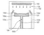
- FIG. 1is a simplified cross-sectional view of an apparatus with which the invention can be implemented.
- FIG. 2is a flow chart of a method, according to an embodiment of the invention, for forming a metal layer on a substrate.
- FIG. 3is a cross-sectional view of a semiconductor substrate after completion of a cold metal deposition step of a method according to the invention.
- FIG. 4Ais a cross-sectional view of a portion of a semiconductor substrate after partial completion of a hot metal deposition step of a method according to the invention.
- FIG. 4Bis a cross-sectional view of a portion of a semiconductor substrate during a hot metal deposition step of a previous hot metal deposition method, after deposition of about the same amount of metal as that shown in FIG. 4 A.
- FIG. 5Ais a cross-sectional view of the portion of the semiconductor substrate shown in FIG. 4A, at a later time during the hot metal deposition step than that shown in FIG. 4 A.
- FIG. 5Bis a cross-sectional view of a portion of a semiconductor substrate during a hot metal deposition step of a previous hot metal deposition method, after deposition of about the same amount of metal as that shown in FIG. 5 A.
- FIG. 6Ais a cross-sectional view of the portion of the semiconductor substrate shown in FIGS. 4A and 5A, near completion of the hot metal deposition step shown partially completed in FIGS. 4A and 5A.
- FIG. 6Bis a cross-sectional view of a portion of a semiconductor substrate during a hot metal deposition step of a previous hot metal deposition method, after deposition of about the same amount of metal as that shown in FIG. 6 A.
- FIG. 7is a flow chart of a method, according to another embodiment of the invention, for forming a metal layer on a substrate.
- FIG. 8is a cross-sectional view of a semiconductor substrate on which various layers of metal have been formed, illustrating several applications of a method according to the invention.
- FIG. 1is a simplified cross-sectional view of an apparatus with which the invention can be implemented.
- the apparatusis a conventional sputtering chamber.
- the apparatuscan be any apparatus that is configured to enable a metal to be deposited on a surface of a substrate.
- a substrate 101e.g., a semiconductor wafer
- the process chamber 102is held at a vacuum pressure and a sputtering gas is injected into the process chamber 102 through one or more gas jets (two gas jets 103 a and 103 b are shown in FIG. 1 ), the gas is ionized, and the ions are accelerated toward a sputtering target 104 .
- a metal to be deposited on a surface of the substrate 101(the upper surface as shown in FIG.
- the substrate 101may be supported on a substrate support surface 106 a of a substrate support 106 .
- metalis deposited on the upper substrate surface while the substrate 101 is supported on the substrate support surface 106 a .
- a heated gasshown generally by the arrow designated by the numeral 107 ) flows through a channel 106 b formed in the substrate support 106 to impact a surface (the bottom surface as shown in FIG.
- FIG. 1shows a single heating gas inlet (channel 106 b ), it is to be understood that the heating gas can be supplied through any number of heating gas inlets, that the heating gas inlets can be positioned at any location proximate to the substrate bottom surface, and that the heating gas inlets can be configured to impinge the heating gas against the substrate 101 at any angle.
- the inventioncan be implemented, for example, using an Endura sputtering system made by Applied Materials of Santa Clara, Calif.
- exemplary magnitudesare given for certain aspects of the invention, such as heating gas and sputtering gas flow rates, heating gas temperatures, substrate temperatures, and duration of certain process steps. These magnitudes relate particularly to implementation of the invention using an Endura sputtering system. However, the magnitudes are expected to be similar for other sputtering systems. The qualitative relationships of such quantities are also expected to be the same.
- relationships between certain quantitiesare expected to be approximately the same for other sputtering systems, such as, for example, the ratio of the sputtering gas flow rate to the heating gas flow rate, and the relative durations of certain steps of methods of the invention and previous hot metal methods.
- FIG. 2is a flow chart of a method 200 , according to an embodiment of the invention, for forming a metal layer on a substrate.
- the method 200includes a “cold” deposition step 201 in which the metal is deposited while the substrate is at a relatively low temperature and a “hot” deposition step 202 in which the metal is deposited while the substrate is at a relatively high temperature. Heating of the substrate during the hot deposition step 202 causes the metal deposited during the cold deposition step 201 (and, eventually, metal subsequently deposited during the hot deposition step 202 ) to heat up.
- Heating of the metal deposited on the substrateincreases the mobility of the metal atoms, thereby causing the metal to disperse more evenly over the substrate surface and decreasing the tendency of the metal to cusp and/or void.
- a key aspect of the inventionis that the substrate is heated more rapidly during the hot deposition step than has been the case in other metallization methods including a hot deposition step.
- the mobility of the metal atomsis increased more quickly than has previously been the case.
- the mobility of atoms distant from the surface of the substrateis increased more quickly than in other methods, thus inhibiting cusping and/or voiding more effectively than has previously been possible.
- a first amount of the metalis deposited on the substrate surface.
- the temperature of the substrateis typically elevated above the ambient atmospheric temperature.
- the first amountis deposited shortly after the wafer has been processed in some other manner, such as deposition of a wetting layer of titanium or titanium-tungsten, that causes the temperature of the wafer to be elevated.
- the temperature of the wafer during the step 201can be from about 40° C. to about 250° C., and preferably about 200° C. (As will be apparent from the description below, this temperature is less than the temperature of the wafer during the step 202 ; hence the step 201 is referred to as the “cold” deposition step.)
- the substrateis heated from the temperature during the cold deposition step 201 (the initial temperature or “cold temperature”) to a target (“hot”) temperature.
- the target temperatureis chosen as a tradeoff between the beneficial increased mobility of metal atoms of the deposited metal layer that is associated with an increase in the target temperature, and the detrimental increased chance of causing damage to the substrate (such as, for example, causing reflow of metallization that has been previously formed on the substrate) that is also associated with an increase in the target temperature.
- the substratecan be heated to a temperature of up to about 500° C. when forming a first layer of aluminum on the substrate, and about 430° C. when forming a second layer of aluminum on the substrate.
- the temperature of the argonis established as about 550° C. and 500° C., respectively, to heat the substrate to those temperatures.
- the inventionheats up the substrate more quickly than has previously been the case.
- the substrateis heated from the initial or cold temperature to about 95% of the target temperature at an average rate that is greater than or equal to about 10° C. /sec.
- the substrateis so heated at an average rate that is greater than or equal to about 15° C. /sec.
- the substrateis so heated at an average rate that is greater than or equal to about 25° C. /sec.
- the heating gasis argon
- the metalis aluminum, and the substrate is heated from an initial temperature of about 200° C.
- the inventionenables the substrate to be heated to about 95% of the target hot temperature in about 10 seconds.
- one previous hot metal methodrequires from 30 seconds to a minute to heat the substrate to the target temperature under the same conditions.
- the substratecan be heated by impinging a heated gas against the substrate as described above with respect to FIG. 1 .
- Any appropriate gascan be used as the heating gas (e.g., any gas that doesn't react with the metal being deposited or other materials formed on or in the substrate), though the heating gas should be the same as other gas(es) used in the process chamber, e.g., the sputtering gas injected into the process chamber 102 through the gas jets 103 a and 103 b in FIG. 1 .
- any inert gassuch as helium, neon or argon can be used.
- Argonin particular, is a typical gas used to sputter metal, and is well-suited for use with the invention.
- a hot deposition stephas been implemented by heating a semiconductor wafer with argon gas while sputtering aluminum.
- a hot deposition stephas been implemented by heating a semiconductor wafer with argon gas while sputtering aluminum.
- the argonis flowed against the substrate at a rate of less than or equal to about 15 sccm (e.g., 10-15 sccm) at a temperature of between 450° C. to 550° C. for a period of greater than or equal to about 4 minutes.
- argon for use in sputteringis also flowed into the process chamber at a rate of about 40 sccm (e.g., 30-50 sccm).
- the combined gasflows, together with the operation of a standard exhaust mechanism, create a pressure of 2 mtorr in the process chamber. It has been believed that chamber pressures higher than about 2 mtorr are undesirable because, for example, chamber pressures above that magnitude result in a longest mean free path of the metal atoms being deposited that is too small to ensure that an adequate number of metal atoms reach the bottom of vias (particularly those with relatively high aspect ratios). Thus, it has been thought necessary to maintain a combined gas flow having a magnitude as described above to ensure a sufficiently low chamber pressure.
- the inventionenables a substrate to be heated up during the hot metal deposition step at a rate faster than heretofore possible by increasing the flow rate of a heating gas used to heat the substrate above the flow rates that have previously been thought feasible.
- the flow rate of the heating gasis greater than or equal to about 15 sccm.
- the flow rate of the heating gasis greater than or equal to about 20 sccm.
- the flow rate of the heating gasis greater than or equal to about 30 sccm.
- the flow rate of the heating gasis greater than or equal to about 40 sccm.
- the flow rate of the sputtering gascan also be increased to reduce or minimize such differential pressure.
- the flow rate of the sputtering gasis greater than or equal to about 2 times the flow rate of the heating gas, and in another embodiment, the flow rate of the sputtering gas is greater than or equal to about 2.5 times the flow rate of the heating gas.
- the flow rate of the sputtering gasis less than or equal to about 4 times the flow rate of the heating gas, and in yet another embodiment, the flow rate of the sputtering gas is less than or equal to about 3 times the flow rate of the heating gas.
- the flow rates of the sputtering gas and the heating gasare controlled so that the differential pressure across the substrate is not sufficient to cause the substrate to experience mechanical failure, and so that the pressure within the process chamber is greater than or equal to about 2 mtorr.
- the chamber pressureis greater than or equal to about 3 mtorr, and in a still further embodiment, the chamber pressure is greater or equal to 4 mtorr.
- the chamber pressurecan be controlled by, in addition to control of the gas flow rates, control of the exhaust mechanism (e.g., varying of the exhaust pump speed, employing an exhaust means equipped with a check valve or pressure regulator, etc.).
- the flow rate of the sputtering gasis greater than or equal to about 40 sccm and the flow rate of the heating gas is greater than or equal to about 15 sccm. In further particular embodiment, the flow rate of the sputtering gas is greater than or equal to about 50 sccm and the flow rate of the heating gas is greater than or equal to about 20 sccm. In a still further particular embodiment, the flow rate of the sputtering gas is greater than or equal to about 80 sccm and the flow rate of the heating gas is greater than or equal to about 30 sccm. In this last embodiment, the chamber pressure is about 6 mtorr.
- the flow rate of the heating gas and the chamber pressureare increased above that previously thought to be the maximum desirable magnitudes, without significant adverse consequences.
- the inventionenables a hot deposition step to be completed more quickly than previously possible (e.g., less than or equal to about 3 minutes for a hot deposition step that, as discussed above, required 3-5 minutes in one previous hot metal method), with formation of few or no voids in the deposited metal layer. It is believed that this is so, notwithstanding the likely decrease (associated with the increased chamber pressure) in mean free path of the metal atoms being deposited, because that detrimental effect (if present) is more than offset by the beneficial effect of increased mobility of the deposited metal atoms that results from the rapid increase in substrate temperature.
- the temperature of the heating gashas been tried as a means to quicken the rate at which the substrate temperature is increased.
- thishas been found to be undesirable, since the substrate temperature is increased more than desired (increasing the chances of damaging previously deposited metal layers or structures on or in the substrate).
- the inventionenables the substrate to be heated rapidly without increasing the temperature of the heating gas.
- the chamber pressureis lower during the step 201 than during the hot deposition step 202 , thus enabling the metal to be deposited more quickly during the cold deposition step 201 than during the hot deposition step 202 .
- the metal atomsare not as mobile during the cold deposition step 201 as during the hot deposition step 202 , increasing the likelihood that cusping and/or voiding may occur as metal is deposited into high aspect ratio vias or deep steps during the cold deposition step 201 .
- the cold deposition step 201is desirably made short to minimize or eliminate problems with cusping and/or voiding.
- the step 201is performed for a predetermined amount of time that is sufficiently long to ensure that the metal is deposited to cover the substrate surface.
- the exact length of the predetermined amount of timecan vary according to a variety of process parameters, such as the metal being deposited, the type of sputtering gas and the geometry (e.g., via aspect ratio, step height) on which the metal is being deposited.
- an amount of metal less than or equal to about 25% of the overall thickness of the metal layer to be formedcan be deposited during the cold deposition step 201 .
- the cold deposition step 201can be performed for less than or equal to about 10 seconds.
- FIG. 3is a cross-sectional view of a semiconductor substrate after completion of a cold metal deposition step of a method according to the invention, e.g., the cold deposition step 201 of the method 200 .
- the cold deposition step 201 of the method 200is similar to that of the cold deposition step of the previous hot metal method described above, the cross-sectional view of FIG. 3 is also illustrative of a semiconductor substrate after completion of the cold step of that previous hot metal method.
- the metal 301 shown in FIG. 3is a first amount deposited during the cold metal deposition step of the invention.
- the metal 301may be deposited in a via 304 formed in oxide 302 that was previously formed over a metal layer 305 .
- a wetting layer 303(described in more detail below) is also shown in FIG. 3 . While the wetting layer 303 need not necessarily be present, the presence of the wetting layer 303 can, in practice, increase the yield associated with the method of the invention. As can be seen, at the end of the cold metal deposition step, the thickness of the metal 301 is relatively small, e.g., perhaps 25% or less of the overall thickness of the layer of metal produced by the method of the invention.
- FIGS. 4A, 5 A and 6 Aare cross-sectional views of a portion of the semiconductor substrate shown in FIG. 3 after progressively greater completion of a hot metal deposition step of a method according to the invention.
- FIGS. 4B, 5 B and 6 Bare cross-sectional views of the same portion of the semiconductor substrate after deposition of an amount of metal similar to that shown in the corresponding FIGS. 4A, 5 A and 6 A during a previous hot metal deposition method.
- cusps 312 a and 312 bare beginning to form where the metal 311 is deposited over the corners of the oxide 302 .
- the metal 301smoothly fills in the via 304 .
- the greater mobility of the atoms of the metal 301as compared to the atoms of the metal 311 , caused by the more rapid heating of the substrate, produces this result.
- Comparison of FIGS. 5A and 5Bshows that the difference in results produced by the method of the invention and the previous hot metal deposition method has been accentuated over time.
- the cusps 312 a and 312 b produced by the previous hot metal deposition methodjoin so that a void 313 is formed.
- the present methodresults in the metal 301 smoothly filling the via 304 .
- FIG. 7is a flow chart of a method 700 , according to another embodiment of the invention, for forming a metal layer on a substrate.
- the step 201is performed, as described above with respect to the method 200 shown in FIG. 2, to deposit a first amount of metal.
- the step 201can be performed for a period of time necessary to ensure that the entire surface on which the metal layer is to be formed is covered with metal; illustratively, the step 201 can be performed for about 10 seconds when aluminum is being deposited using argon as a sputtering gas.
- a step 702is performed in which the substrate is heated while a second amount of metal is deposited on the first amount deposited during the step 201 .
- the step 702is similar to the step 202 of the method 200 described above (FIG. 2 ), differing only in the duration of the step: unlike the step 202 , the step 702 is not performed until deposition of the remaining metal necessary to form a metal layer of desired thickness, and is, therefore, typically shorter in duration than the step 202 .
- the step 702can be performed for a specified amount of time or until a specified amount of metal has been deposited.
- the step 702when aluminum is being deposited using argon as a sputtering gas, the step 702 can be performed for about 2 minutes when the step 702 and a cold metal deposition step 703 (described below) having a duration of 10 seconds are performed in place of a hot deposition step 202 having a duration of 3 minutes.
- a cold metal deposition step 703described below
- the method 700ends with the step 703 in which a second cold deposition is performed.
- the step 703is similar to the step 201 in that heat is not supplied to the substrate. However, typically, the temperature of the substrate during the cold deposition step 703 is higher than that during the cold deposition step 201 , since the substrate has been heated up during the hot deposition step 702 .
- the remaining metal necessary to form a metal layer of the desired thicknessis deposited.
- the step 703can be performed for about 10 seconds (as discussed above).
- a cold deposition stepcan deposit metal at a faster rate than a hot deposition step (a ten second cold deposition step 703 in the method 700 can replace approximately the last minute of the hot deposition step 202 of the method 200 ), and since the danger of cusping and voiding is relatively minimal near the end of the deposition of a metal layer, the use of a cold deposition step to finish the deposition can advantageously shorten the overall time required to deposit the metal layer, with little increase in the danger of formation of defects in the metal layer.
- the cold and hot deposition steps of the methods 200 and 700can advantageously be performed in the same process chamber, thus avoiding the decrease in throughput associated with moving the substrate between process chambers.
- a method according to the inventioncan also be implemented so that more than one process chamber is used to implement the steps of the method.
- a conventional degassing procedurecan be performed to remove moisture from a dielectric layer or layers on which a metal layer or layers are to be formed.
- a conventional etching proceduree.g., a conventional sputter etch procedure
- a conventional etching procedurecan be performed to remove portions of the dielectric layer(s) to create vias or steps.
- a wetting layere.g., 100 to 300 angstroms of titanium, a composition of titanium and tungsten, or other suitable material
- a method according to the inventionis used to deposit the desired amount of metal in the desired location or locations.
- the metal depositioncan be followed by further processing steps, such as a conventional anti-reflective coating (ARC), using conventional techniques.
- ARCanti-reflective coating
- the substratecan be cooled according to a standard cooling procedure for a specified time (e.g., 30 seconds).
- FIG. 8is a cross-sectional view of a semiconductor substrate on which various metal layers have been formed, illustrating several applications of a method according to the invention.
- a metal layer 804 formed on the dielectric layer 802may be electrically connected to a polysilicon gate 809 formed on oxide 810 by a metal contact 806 that extends through a dielectric layer 802 .
- metal layer 804may be electrically connected to an electrically doped region 811 of the silicon substrate 801 by a metal contact 807 that extends through a dielectric layer 802 .
- a second metal layer 805 formed on the dielectric layer 803 that overlies the first metal layer 804may be electrically connected to the first metal layer 804 by a metal contact 808 that extends through the dielectric layer 803 .
- a barrier layerpreventing or inhibiting migration of silicon atoms into the aluminum may be necessary. Examples of such a barrier layer include titanium-tungsten alloy or titanium-nitride.
- the barrier layermay have a layer (such as titanium) between it and the underlying structure that reduces contact resistance.
- the inventionis broadly applicable to the formation of a metal layer on any type of substrate or device.
- formation of a metal layer according to the inventioncan be accomplished on any type of semiconductor substrate, such as a semiconductor wafer.
- the inventioncan be used to form metal layers in active electronic components (e.g., integrated circuit chips, transistors and diodes) and passive electronic components (e.g., resistors, capacitors and inductors).
- active electronic componentse.g., integrated circuit chips, transistors and diodes
- passive electronic componentse.g., resistors, capacitors and inductors
- the inventioncan also be used to form metal layers in other types of devices, such as lead frames, medical devices, disks and heads, flat panel displays and microelectronic masks.
Landscapes
- Engineering & Computer Science (AREA)
- Physics & Mathematics (AREA)
- Condensed Matter Physics & Semiconductors (AREA)
- General Physics & Mathematics (AREA)
- Manufacturing & Machinery (AREA)
- Computer Hardware Design (AREA)
- Microelectronics & Electronic Packaging (AREA)
- Power Engineering (AREA)
- Electrodes Of Semiconductors (AREA)
- Physical Vapour Deposition (AREA)
Abstract
Description
Claims (22)
Priority Applications (1)
| Application Number | Priority Date | Filing Date | Title |
|---|---|---|---|
| US09/866,957US6627547B2 (en) | 1996-08-01 | 2001-05-29 | Hot metallization process |
Applications Claiming Priority (2)
| Application Number | Priority Date | Filing Date | Title |
|---|---|---|---|
| US08/693,978US6309971B1 (en) | 1996-08-01 | 1996-08-01 | Hot metallization process |
| US09/866,957US6627547B2 (en) | 1996-08-01 | 2001-05-29 | Hot metallization process |
Related Parent Applications (1)
| Application Number | Title | Priority Date | Filing Date |
|---|---|---|---|
| US08/693,978ContinuationUS6309971B1 (en) | 1996-08-01 | 1996-08-01 | Hot metallization process |
Publications (2)
| Publication Number | Publication Date |
|---|---|
| US20010036717A1 US20010036717A1 (en) | 2001-11-01 |
| US6627547B2true US6627547B2 (en) | 2003-09-30 |
Family
ID=24786919
Family Applications (2)
| Application Number | Title | Priority Date | Filing Date |
|---|---|---|---|
| US08/693,978Expired - LifetimeUS6309971B1 (en) | 1996-08-01 | 1996-08-01 | Hot metallization process |
| US09/866,957Expired - LifetimeUS6627547B2 (en) | 1996-08-01 | 2001-05-29 | Hot metallization process |
Family Applications Before (1)
| Application Number | Title | Priority Date | Filing Date |
|---|---|---|---|
| US08/693,978Expired - LifetimeUS6309971B1 (en) | 1996-08-01 | 1996-08-01 | Hot metallization process |
Country Status (2)
| Country | Link |
|---|---|
| US (2) | US6309971B1 (en) |
| TW (1) | TW379386B (en) |
Cited By (3)
| Publication number | Priority date | Publication date | Assignee | Title |
|---|---|---|---|---|
| US7189645B1 (en) | 2004-04-26 | 2007-03-13 | National Semiconductor Corporation | System and method for adjusting the ratio of deposition times to optimize via density and via fill in aluminum multilayer metallization |
| US7259096B2 (en) | 2003-12-31 | 2007-08-21 | Dongbu Electronics Co., Ltd. | Method for forming aluminum interconnect |
| US11560751B2 (en) | 2019-09-11 | 2023-01-24 | Catalyst Acoustics Group, Inc. | Sound damping door |
Families Citing this family (5)
| Publication number | Priority date | Publication date | Assignee | Title |
|---|---|---|---|---|
| JP3033564B2 (en)* | 1997-10-02 | 2000-04-17 | セイコーエプソン株式会社 | Method for manufacturing semiconductor device |
| US6979640B1 (en) | 2002-03-29 | 2005-12-27 | Cypress Semiconductor Corporation | Contact structure and method of making the same |
| JP4434825B2 (en)* | 2003-05-08 | 2010-03-17 | パナソニック株式会社 | Impulse waveform generator |
| US7901976B1 (en) | 2006-05-18 | 2011-03-08 | Cypress Semiconductor Corporation | Method of forming borderless contacts |
| DE102010028458A1 (en)* | 2010-04-30 | 2011-11-03 | Globalfoundries Dresden Module One Llc & Co. Kg | Semiconductor device having contact elements and Metallsilizidgebieten, which are made in a common process sequence |
Citations (69)
| Publication number | Priority date | Publication date | Assignee | Title |
|---|---|---|---|---|
| US3848330A (en) | 1972-06-01 | 1974-11-19 | Motorola Inc | Electromigration resistant semiconductor contacts and the method of producing same |
| US4600658A (en) | 1983-11-07 | 1986-07-15 | Motorola, Inc. | Metallization means and method for high temperature applications |
| WO1986006755A1 (en) | 1985-05-10 | 1986-11-20 | General Electric Company | Selective chemical vapor deposition method and apparatus |
| US4786962A (en) | 1986-06-06 | 1988-11-22 | Hewlett-Packard Company | Process for fabricating multilevel metal integrated circuits and structures produced thereby |
| US4789648A (en) | 1985-10-28 | 1988-12-06 | International Business Machines Corporation | Method for producing coplanar multi-level metal/insulator films on a substrate and for forming patterned conductive lines simultaneously with stud vias |
| EP0351001A1 (en) | 1988-07-12 | 1990-01-17 | Koninklijke Philips Electronics N.V. | Method for making a semi-conductor device with at least one level of interconnection with small dimensioned via holes |
| US4933743A (en) | 1989-03-11 | 1990-06-12 | Fairchild Semiconductor Corporation | High performance interconnect system for an integrated circuit |
| US4933304A (en) | 1988-11-03 | 1990-06-12 | Sgs-Thomson Microelectronics, Inc. | Method for reducing the surface reflectance of a metal layer during semiconductor processing |
| US4954142A (en) | 1989-03-07 | 1990-09-04 | International Business Machines Corporation | Method of chemical-mechanical polishing an electronic component substrate and polishing slurry therefor |
| US4956313A (en) | 1987-08-17 | 1990-09-11 | International Business Machines Corporation | Via-filling and planarization technique |
| US4962060A (en) | 1987-03-10 | 1990-10-09 | Advanced Micro Devices, Inc. | Making a high speed interconnect system with refractory non-dogbone contacts and an active electromigration suppression mechanism |
| US4970176A (en) | 1989-09-29 | 1990-11-13 | Motorola, Inc. | Multiple step metallization process |
| EP0420597A2 (en) | 1989-09-26 | 1991-04-03 | Canon Kabushiki Kaisha | Process for forming a deposited film by use of alkyl aluminum hydride and process for preparing semiconductor device |
| EP0420595A2 (en) | 1989-09-26 | 1991-04-03 | Canon Kabushiki Kaisha | Deposited film formation method utilizing selective deposition by use of alkyl aluminum hydride |
| EP0425084A1 (en) | 1989-09-09 | 1991-05-02 | Canon Kabushiki Kaisha | Process for forming deposited film by use of alkyl aluminum hydride |
| EP0439128A2 (en) | 1990-01-22 | 1991-07-31 | Sumitomo Electric Industries, Ltd. | Housing for semiconductor device and method of manufacturing |
| US5053351A (en) | 1991-03-19 | 1991-10-01 | Micron Technology, Inc. | Method of making stacked E-cell capacitor DRAM cell |
| EP0451740A2 (en) | 1990-04-09 | 1991-10-16 | Anelva Corporation | Temperature control system for semiconductor wafer or substrate |
| EP0451571A2 (en) | 1990-03-30 | 1991-10-16 | Applied Materials, Inc. | Sputtering process for forming aluminum layer over stepped semiconductor wafer |
| US5066615A (en) | 1989-10-23 | 1991-11-19 | At&T Bell Laboratories | Photolithographic processes using thin coatings of refractory metal silicon nitrides as antireflection layers |
| US5071714A (en) | 1989-04-17 | 1991-12-10 | International Business Machines Corporation | Multilayered intermetallic connection for semiconductor devices |
| US5093279A (en) | 1991-02-01 | 1992-03-03 | International Business Machines Corporation | Laser ablation damascene process |
| US5108951A (en) | 1990-11-05 | 1992-04-28 | Sgs-Thomson Microelectronics, Inc. | Method for forming a metal contact |
| US5128009A (en) | 1989-11-30 | 1992-07-07 | Siemens Aktiengesellschaft | Process for reducing the reflectivity of sputtered films |
| EP0499241A1 (en) | 1991-02-12 | 1992-08-19 | Applied Materials, Inc. | Sputtering process for forming aluminum layer over stepped semiconductor wafer |
| US5158933A (en) | 1990-11-15 | 1992-10-27 | Holtz Ronald L | Phase separated composite materials |
| US5202279A (en) | 1990-12-05 | 1993-04-13 | Texas Instruments Incorporated | Poly sidewall process to reduce gated diode leakage |
| US5236868A (en) | 1990-04-20 | 1993-08-17 | Applied Materials, Inc. | Formation of titanium nitride on semiconductor wafer by reaction of titanium with nitrogen-bearing gas in an integrated processing system |
| US5242860A (en) | 1991-07-24 | 1993-09-07 | Applied Materials, Inc. | Method for the formation of tin barrier layer with preferential (111) crystallographic orientation |
| US5245210A (en) | 1990-08-11 | 1993-09-14 | Nec Corporation | MOS type semiconductor device |
| US5262354A (en) | 1992-02-26 | 1993-11-16 | International Business Machines Corporation | Refractory metal capped low resistivity metal conductor lines and vias |
| US5267607A (en) | 1991-05-28 | 1993-12-07 | Tokyo Electron Limited | Substrate processing apparatus |
| US5270255A (en) | 1993-01-08 | 1993-12-14 | Chartered Semiconductor Manufacturing Pte, Ltd. | Metallization process for good metal step coverage while maintaining useful alignment mark |
| US5286674A (en) | 1992-03-02 | 1994-02-15 | Motorola, Inc. | Method for forming a via structure and semiconductor device having the same |
| US5288665A (en) | 1992-08-12 | 1994-02-22 | Applied Materials, Inc. | Process for forming low resistance aluminum plug in via electrically connected to overlying patterned metal layer for integrated circuit structures |
| US5302266A (en) | 1992-03-20 | 1994-04-12 | International Business Machines Corporation | Method and apparatus for filing high aspect patterns with metal |
| US5312512A (en) | 1992-10-23 | 1994-05-17 | Ncr Corporation | Global planarization using SOG and CMP |
| US5313089A (en) | 1992-05-26 | 1994-05-17 | Motorola, Inc. | Capacitor and a memory cell formed therefrom |
| US5312777A (en) | 1992-09-25 | 1994-05-17 | International Business Machines Corporation | Fabrication methods for bidirectional field emission devices and storage structures |
| US5358616A (en) | 1993-02-17 | 1994-10-25 | Ward Michael G | Filling of vias and contacts employing an aluminum-germanium alloy |
| US5360524A (en) | 1993-04-13 | 1994-11-01 | Rudi Hendel | Method for planarization of submicron vias and the manufacture of semiconductor integrated circuits |
| US5371047A (en) | 1992-10-30 | 1994-12-06 | International Business Machines Corporation | Chip interconnection having a breathable etch stop layer |
| US5371042A (en) | 1992-06-16 | 1994-12-06 | Applied Materials, Inc. | Method of filling contacts in semiconductor devices |
| US5374592A (en) | 1992-09-22 | 1994-12-20 | Sgs-Thomson Microelectronics, Inc. | Method for forming an aluminum metal contact |
| US5378660A (en) | 1993-02-12 | 1995-01-03 | Applied Materials, Inc. | Barrier layers and aluminum contacts |
| US5380678A (en) | 1991-03-12 | 1995-01-10 | Yu; Chang | Bilayer barrier metal method for obtaining 100% step-coverage in contact vias without junction degradation |
| US5393565A (en) | 1992-06-08 | 1995-02-28 | Fujitsu Limited | Method for deposition of a refractory metal nitride and method for formation of a conductive film containing a refractory metal nitride |
| US5397741A (en) | 1993-03-29 | 1995-03-14 | International Business Machines Corporation | Process for metallized vias in polyimide |
| US5443995A (en) | 1993-09-17 | 1995-08-22 | Applied Materials, Inc. | Method for metallizing a semiconductor wafer |
| US5453639A (en) | 1992-09-04 | 1995-09-26 | International Business Machines Corporation | Planarized semiconductor structure using subminimum features |
| US5459354A (en) | 1992-12-25 | 1995-10-17 | Nippon Steel Corporation | Semiconductor device with improved insulation of wiring structure from a gate electrode |
| US5468342A (en) | 1994-04-28 | 1995-11-21 | Cypress Semiconductor Corp. | Method of etching an oxide layer |
| US5470792A (en) | 1993-03-03 | 1995-11-28 | Nec Corporation | Method of manufacturing semiconductor device |
| US5496771A (en) | 1994-05-19 | 1996-03-05 | International Business Machines Corporation | Method of making overpass mask/insulator for local interconnects |
| US5523259A (en) | 1994-12-05 | 1996-06-04 | At&T Corp. | Method of forming metal layers formed as a composite of sub-layers using Ti texture control layer |
| US5539255A (en) | 1995-09-07 | 1996-07-23 | International Business Machines Corporation | Semiconductor structure having self-aligned interconnection metallization formed from a single layer of metal |
| US5578524A (en) | 1994-03-30 | 1996-11-26 | Nec Corporation | Fabrication process of a semiconductor device with a wiring structure |
| US5592024A (en) | 1993-10-29 | 1997-01-07 | Kabushiki Kaisha Toshiba | Semiconductor device having a wiring layer with a barrier layer |
| US5600182A (en) | 1995-01-24 | 1997-02-04 | Lsi Logic Corporation | Barrier metal technology for tungsten plug interconnection |
| US5651855A (en) | 1992-07-28 | 1997-07-29 | Micron Technology, Inc. | Method of making self aligned contacts to silicon substrates during the manufacture of integrated circuits |
| EP0790641A1 (en) | 1996-02-16 | 1997-08-20 | Novellus Systems, Inc. | Wafer cooling device |
| US5665659A (en) | 1993-06-10 | 1997-09-09 | Samsung Electronics Co., Ltd. | Method for forming metal layer of a semiconductor device |
| US5691571A (en) | 1994-12-28 | 1997-11-25 | Nec Corporation | Semiconductor device having fine contact hole with high aspect ratio |
| US5693564A (en) | 1994-12-22 | 1997-12-02 | Intel Corporation | Conductor fill reflow with intermetallic compound wetting layer for semiconductor fabrication |
| US5731245A (en) | 1994-08-05 | 1998-03-24 | International Business Machines Corp. | High aspect ratio low resistivity lines/vias with a tungsten-germanium alloy hard cap |
| US5804251A (en) | 1995-12-29 | 1998-09-08 | Intel Corporation | Low temperature aluminum alloy plug technology |
| US5807760A (en) | 1990-12-19 | 1998-09-15 | Lucent Technologies Inc. | Method of despositing an aluminum-rich layer |
| US5962923A (en) | 1995-08-07 | 1999-10-05 | Applied Materials, Inc. | Semiconductor device having a low thermal budget metal filling and planarization of contacts, vias and trenches |
| US6045666A (en) | 1995-08-07 | 2000-04-04 | Applied Materials, Inc. | Aluminum hole filling method using ionized metal adhesion layer |
- 1996
- 1996-08-01USUS08/693,978patent/US6309971B1/ennot_activeExpired - Lifetime
- 1997
- 1997-10-15TWTW086115129Apatent/TW379386B/ennot_activeIP Right Cessation
- 2001
- 2001-05-29USUS09/866,957patent/US6627547B2/ennot_activeExpired - Lifetime
Patent Citations (74)
| Publication number | Priority date | Publication date | Assignee | Title |
|---|---|---|---|---|
| US3848330A (en) | 1972-06-01 | 1974-11-19 | Motorola Inc | Electromigration resistant semiconductor contacts and the method of producing same |
| US4600658A (en) | 1983-11-07 | 1986-07-15 | Motorola, Inc. | Metallization means and method for high temperature applications |
| WO1986006755A1 (en) | 1985-05-10 | 1986-11-20 | General Electric Company | Selective chemical vapor deposition method and apparatus |
| EP0223787A1 (en) | 1985-05-10 | 1987-06-03 | Gen Electric | Selective chemical vapor deposition method and apparatus. |
| US4789648A (en) | 1985-10-28 | 1988-12-06 | International Business Machines Corporation | Method for producing coplanar multi-level metal/insulator films on a substrate and for forming patterned conductive lines simultaneously with stud vias |
| US4786962A (en) | 1986-06-06 | 1988-11-22 | Hewlett-Packard Company | Process for fabricating multilevel metal integrated circuits and structures produced thereby |
| US4962060A (en) | 1987-03-10 | 1990-10-09 | Advanced Micro Devices, Inc. | Making a high speed interconnect system with refractory non-dogbone contacts and an active electromigration suppression mechanism |
| US4956313A (en) | 1987-08-17 | 1990-09-11 | International Business Machines Corporation | Via-filling and planarization technique |
| EP0351001A1 (en) | 1988-07-12 | 1990-01-17 | Koninklijke Philips Electronics N.V. | Method for making a semi-conductor device with at least one level of interconnection with small dimensioned via holes |
| US4933304A (en) | 1988-11-03 | 1990-06-12 | Sgs-Thomson Microelectronics, Inc. | Method for reducing the surface reflectance of a metal layer during semiconductor processing |
| US4954142A (en) | 1989-03-07 | 1990-09-04 | International Business Machines Corporation | Method of chemical-mechanical polishing an electronic component substrate and polishing slurry therefor |
| US4933743A (en) | 1989-03-11 | 1990-06-12 | Fairchild Semiconductor Corporation | High performance interconnect system for an integrated circuit |
| US5071714A (en) | 1989-04-17 | 1991-12-10 | International Business Machines Corporation | Multilayered intermetallic connection for semiconductor devices |
| EP0425084A1 (en) | 1989-09-09 | 1991-05-02 | Canon Kabushiki Kaisha | Process for forming deposited film by use of alkyl aluminum hydride |
| EP0420597A2 (en) | 1989-09-26 | 1991-04-03 | Canon Kabushiki Kaisha | Process for forming a deposited film by use of alkyl aluminum hydride and process for preparing semiconductor device |
| EP0420595A2 (en) | 1989-09-26 | 1991-04-03 | Canon Kabushiki Kaisha | Deposited film formation method utilizing selective deposition by use of alkyl aluminum hydride |
| US4970176A (en) | 1989-09-29 | 1990-11-13 | Motorola, Inc. | Multiple step metallization process |
| US5066615A (en) | 1989-10-23 | 1991-11-19 | At&T Bell Laboratories | Photolithographic processes using thin coatings of refractory metal silicon nitrides as antireflection layers |
| US5128009A (en) | 1989-11-30 | 1992-07-07 | Siemens Aktiengesellschaft | Process for reducing the reflectivity of sputtered films |
| EP0439128A2 (en) | 1990-01-22 | 1991-07-31 | Sumitomo Electric Industries, Ltd. | Housing for semiconductor device and method of manufacturing |
| US5108570A (en) | 1990-03-30 | 1992-04-28 | Applied Materials, Inc. | Multistep sputtering process for forming aluminum layer over stepped semiconductor wafer |
| EP0451571A2 (en) | 1990-03-30 | 1991-10-16 | Applied Materials, Inc. | Sputtering process for forming aluminum layer over stepped semiconductor wafer |
| EP0451740A2 (en) | 1990-04-09 | 1991-10-16 | Anelva Corporation | Temperature control system for semiconductor wafer or substrate |
| US5236868A (en) | 1990-04-20 | 1993-08-17 | Applied Materials, Inc. | Formation of titanium nitride on semiconductor wafer by reaction of titanium with nitrogen-bearing gas in an integrated processing system |
| US5245210A (en) | 1990-08-11 | 1993-09-14 | Nec Corporation | MOS type semiconductor device |
| US5108951A (en) | 1990-11-05 | 1992-04-28 | Sgs-Thomson Microelectronics, Inc. | Method for forming a metal contact |
| US5158933A (en) | 1990-11-15 | 1992-10-27 | Holtz Ronald L | Phase separated composite materials |
| US5202279A (en) | 1990-12-05 | 1993-04-13 | Texas Instruments Incorporated | Poly sidewall process to reduce gated diode leakage |
| US5807760A (en) | 1990-12-19 | 1998-09-15 | Lucent Technologies Inc. | Method of despositing an aluminum-rich layer |
| US5093279A (en) | 1991-02-01 | 1992-03-03 | International Business Machines Corporation | Laser ablation damascene process |
| EP0499241A1 (en) | 1991-02-12 | 1992-08-19 | Applied Materials, Inc. | Sputtering process for forming aluminum layer over stepped semiconductor wafer |
| US5380678A (en) | 1991-03-12 | 1995-01-10 | Yu; Chang | Bilayer barrier metal method for obtaining 100% step-coverage in contact vias without junction degradation |
| US5053351A (en) | 1991-03-19 | 1991-10-01 | Micron Technology, Inc. | Method of making stacked E-cell capacitor DRAM cell |
| US5267607A (en) | 1991-05-28 | 1993-12-07 | Tokyo Electron Limited | Substrate processing apparatus |
| US5242860A (en) | 1991-07-24 | 1993-09-07 | Applied Materials, Inc. | Method for the formation of tin barrier layer with preferential (111) crystallographic orientation |
| US5521120A (en) | 1991-07-24 | 1996-05-28 | Applied Materials, Inc. | Method for the formation of tin barrier layer with preferential (111) crystallographic orientation |
| US5434044A (en) | 1991-07-24 | 1995-07-18 | Applied Materials, Inc. | Method for the formation of tin barrier layer with preferential (111) crystallographic orientation |
| US5262354A (en) | 1992-02-26 | 1993-11-16 | International Business Machines Corporation | Refractory metal capped low resistivity metal conductor lines and vias |
| US5286674A (en) | 1992-03-02 | 1994-02-15 | Motorola, Inc. | Method for forming a via structure and semiconductor device having the same |
| US5302266A (en) | 1992-03-20 | 1994-04-12 | International Business Machines Corporation | Method and apparatus for filing high aspect patterns with metal |
| US5313089A (en) | 1992-05-26 | 1994-05-17 | Motorola, Inc. | Capacitor and a memory cell formed therefrom |
| US5393565A (en) | 1992-06-08 | 1995-02-28 | Fujitsu Limited | Method for deposition of a refractory metal nitride and method for formation of a conductive film containing a refractory metal nitride |
| US5371042A (en) | 1992-06-16 | 1994-12-06 | Applied Materials, Inc. | Method of filling contacts in semiconductor devices |
| US5651855A (en) | 1992-07-28 | 1997-07-29 | Micron Technology, Inc. | Method of making self aligned contacts to silicon substrates during the manufacture of integrated circuits |
| US5288665A (en) | 1992-08-12 | 1994-02-22 | Applied Materials, Inc. | Process for forming low resistance aluminum plug in via electrically connected to overlying patterned metal layer for integrated circuit structures |
| US5453639A (en) | 1992-09-04 | 1995-09-26 | International Business Machines Corporation | Planarized semiconductor structure using subminimum features |
| US5374592A (en) | 1992-09-22 | 1994-12-20 | Sgs-Thomson Microelectronics, Inc. | Method for forming an aluminum metal contact |
| US5312777A (en) | 1992-09-25 | 1994-05-17 | International Business Machines Corporation | Fabrication methods for bidirectional field emission devices and storage structures |
| US5312512A (en) | 1992-10-23 | 1994-05-17 | Ncr Corporation | Global planarization using SOG and CMP |
| US5371047A (en) | 1992-10-30 | 1994-12-06 | International Business Machines Corporation | Chip interconnection having a breathable etch stop layer |
| US5459354A (en) | 1992-12-25 | 1995-10-17 | Nippon Steel Corporation | Semiconductor device with improved insulation of wiring structure from a gate electrode |
| US5270255A (en) | 1993-01-08 | 1993-12-14 | Chartered Semiconductor Manufacturing Pte, Ltd. | Metallization process for good metal step coverage while maintaining useful alignment mark |
| US5378660A (en) | 1993-02-12 | 1995-01-03 | Applied Materials, Inc. | Barrier layers and aluminum contacts |
| US5358616A (en) | 1993-02-17 | 1994-10-25 | Ward Michael G | Filling of vias and contacts employing an aluminum-germanium alloy |
| US5470792A (en) | 1993-03-03 | 1995-11-28 | Nec Corporation | Method of manufacturing semiconductor device |
| US5397741A (en) | 1993-03-29 | 1995-03-14 | International Business Machines Corporation | Process for metallized vias in polyimide |
| US5360524A (en) | 1993-04-13 | 1994-11-01 | Rudi Hendel | Method for planarization of submicron vias and the manufacture of semiconductor integrated circuits |
| US5665659A (en) | 1993-06-10 | 1997-09-09 | Samsung Electronics Co., Ltd. | Method for forming metal layer of a semiconductor device |
| US5443995A (en) | 1993-09-17 | 1995-08-22 | Applied Materials, Inc. | Method for metallizing a semiconductor wafer |
| US5592024A (en) | 1993-10-29 | 1997-01-07 | Kabushiki Kaisha Toshiba | Semiconductor device having a wiring layer with a barrier layer |
| US5578524A (en) | 1994-03-30 | 1996-11-26 | Nec Corporation | Fabrication process of a semiconductor device with a wiring structure |
| US5468342A (en) | 1994-04-28 | 1995-11-21 | Cypress Semiconductor Corp. | Method of etching an oxide layer |
| US5496771A (en) | 1994-05-19 | 1996-03-05 | International Business Machines Corporation | Method of making overpass mask/insulator for local interconnects |
| US5731245A (en) | 1994-08-05 | 1998-03-24 | International Business Machines Corp. | High aspect ratio low resistivity lines/vias with a tungsten-germanium alloy hard cap |
| US5523259A (en) | 1994-12-05 | 1996-06-04 | At&T Corp. | Method of forming metal layers formed as a composite of sub-layers using Ti texture control layer |
| US5693564A (en) | 1994-12-22 | 1997-12-02 | Intel Corporation | Conductor fill reflow with intermetallic compound wetting layer for semiconductor fabrication |
| US5691571A (en) | 1994-12-28 | 1997-11-25 | Nec Corporation | Semiconductor device having fine contact hole with high aspect ratio |
| US5600182A (en) | 1995-01-24 | 1997-02-04 | Lsi Logic Corporation | Barrier metal technology for tungsten plug interconnection |
| US5962923A (en) | 1995-08-07 | 1999-10-05 | Applied Materials, Inc. | Semiconductor device having a low thermal budget metal filling and planarization of contacts, vias and trenches |
| US6045666A (en) | 1995-08-07 | 2000-04-04 | Applied Materials, Inc. | Aluminum hole filling method using ionized metal adhesion layer |
| US6217721B1 (en) | 1995-08-07 | 2001-04-17 | Applied Materials, Inc. | Filling narrow apertures and forming interconnects with a metal utilizing a crystallographically oriented liner layer |
| US5539255A (en) | 1995-09-07 | 1996-07-23 | International Business Machines Corporation | Semiconductor structure having self-aligned interconnection metallization formed from a single layer of metal |
| US5804251A (en) | 1995-12-29 | 1998-09-08 | Intel Corporation | Low temperature aluminum alloy plug technology |
| EP0790641A1 (en) | 1996-02-16 | 1997-08-20 | Novellus Systems, Inc. | Wafer cooling device |
Non-Patent Citations (6)
| Title |
|---|
| Robinson, Gail, "Al hits sub-0.25 micron vias," Electronic Engineering Times, Issue 939, Feb. 3, 1997, pp. 37 and 42. |
| Singer, Pete, "The Interconnect Challenge: Filling Small, High Aspect Ratio Contact Holes," Semiconductor International, Aug. 1994, pp. 57-64. |
| Uehara, T. et al., "A Novel Local Interconnect Technology (MSD) for High-Performance Logic LSIs with Embedded SRAM," 1996 Symposium on VLSI Technology Digest of Technical Papers, IEEE, 1996, pp. 142-143. |
| Wolf, Stanley, Silicon Processing for the VLSI Era, vol. 2: Process Integration, 1990, pp. 144-145, 212-214, 354-355. |
| Zheng Xu et al., Al planarization processes for multilayer metallization of quarter micrometer devices, Thin Solid Films 253 (1994), Elsevier Science S.A., pp. 367-371. |
| Zheng Xu et al., Planar Multilevel Metallization Technologies for ULSI Devices, SPIE, vol. 2335, pp. 70-79. |
Cited By (4)
| Publication number | Priority date | Publication date | Assignee | Title |
|---|---|---|---|---|
| US7259096B2 (en) | 2003-12-31 | 2007-08-21 | Dongbu Electronics Co., Ltd. | Method for forming aluminum interconnect |
| US7189645B1 (en) | 2004-04-26 | 2007-03-13 | National Semiconductor Corporation | System and method for adjusting the ratio of deposition times to optimize via density and via fill in aluminum multilayer metallization |
| US7358611B1 (en) | 2004-04-26 | 2008-04-15 | National Semiconductor Corporation | System and method for adjusting the ratio of deposition times to optimize via density and via fill in aluminum multilayer metallization |
| US11560751B2 (en) | 2019-09-11 | 2023-01-24 | Catalyst Acoustics Group, Inc. | Sound damping door |
Also Published As
| Publication number | Publication date |
|---|---|
| US20010036717A1 (en) | 2001-11-01 |
| US6309971B1 (en) | 2001-10-30 |
| TW379386B (en) | 2000-01-11 |
Similar Documents
| Publication | Publication Date | Title |
|---|---|---|
| US10879113B2 (en) | Semiconductor constructions; and methods for providing electrically conductive material within openings | |
| US6323124B1 (en) | Resputtering to achieve better step coverage | |
| KR950009934B1 (en) | Metalizing method of semiconductor device | |
| US5317187A (en) | Ti/TiN/Ti contact metallization | |
| US5527561A (en) | Method for filing substrate recesses using elevated temperature and pressure | |
| US5147819A (en) | Semiconductor metallization method | |
| US20030091870A1 (en) | Method of forming a liner for tungsten plugs | |
| US6410383B1 (en) | Method of forming conducting diffusion barriers | |
| EP0516344B1 (en) | Method to fill a cavity in a substrate | |
| KR960011865B1 (en) | Manufacturing method of metal layer of semiconductor device | |
| US5948467A (en) | Enhanced CVD copper adhesion by two-step deposition process | |
| US20090050468A1 (en) | Controlled surface oxidation of aluminum interconnect | |
| US5582881A (en) | Process for deposition of a Ti/TiN cap layer on aluminum metallization and apparatus | |
| US6627547B2 (en) | Hot metallization process | |
| JPH1070093A (en) | Filling of aluminum hole using ionized metal adhesion layer | |
| KR100231766B1 (en) | Method of fabricating metal layer as interconnector in semiconductor integrated circuit | |
| JPH1074707A (en) | Titanium / aluminide wet layer for aluminum contact | |
| US20080054492A1 (en) | Semiconductor device and method for manufacturing the same | |
| US7224065B2 (en) | Contact/via force fill techniques and resulting structures | |
| KR100485274B1 (en) | Improved metal layer formation method | |
| US6156645A (en) | Method of forming a metal layer on a substrate, including formation of wetting layer at a high temperature | |
| JPH08162531A (en) | Wiring formation | |
| US6365514B1 (en) | Two chamber metal reflow process | |
| JPH1174223A (en) | Method for metal layer forming on substrate | |
| JP2780838B2 (en) | Method for manufacturing semiconductor device |
Legal Events
| Date | Code | Title | Description |
|---|---|---|---|
| STCF | Information on status: patent grant | Free format text:PATENTED CASE | |
| FPAY | Fee payment | Year of fee payment:4 | |
| FPAY | Fee payment | Year of fee payment:8 | |
| AS | Assignment | Owner name:MORGAN STANLEY SENIOR FUNDING, INC., NEW YORK Free format text:SECURITY INTEREST;ASSIGNORS:CYPRESS SEMICONDUCTOR CORPORATION;SPANSION LLC;REEL/FRAME:035240/0429 Effective date:20150312 | |
| FPAY | Fee payment | Year of fee payment:12 | |
| AS | Assignment | Owner name:CYPRESS SEMICONDUCTOR CORPORATION, CALIFORNIA Free format text:PARTIAL RELEASE OF SECURITY INTEREST IN PATENTS;ASSIGNOR:MORGAN STANLEY SENIOR FUNDING, INC., AS COLLATERAL AGENT;REEL/FRAME:039708/0001 Effective date:20160811 Owner name:SPANSION LLC, CALIFORNIA Free format text:PARTIAL RELEASE OF SECURITY INTEREST IN PATENTS;ASSIGNOR:MORGAN STANLEY SENIOR FUNDING, INC., AS COLLATERAL AGENT;REEL/FRAME:039708/0001 Effective date:20160811 | |
| AS | Assignment | Owner name:MORGAN STANLEY SENIOR FUNDING, INC., NEW YORK Free format text:CORRECTIVE ASSIGNMENT TO CORRECT THE 8647899 PREVIOUSLY RECORDED ON REEL 035240 FRAME 0429. ASSIGNOR(S) HEREBY CONFIRMS THE SECURITY INTERST;ASSIGNORS:CYPRESS SEMICONDUCTOR CORPORATION;SPANSION LLC;REEL/FRAME:058002/0470 Effective date:20150312 |