US6626734B2 - Method and apparatus for wireless transfer of chemical-mechanical planarization measurements - Google Patents
Method and apparatus for wireless transfer of chemical-mechanical planarization measurementsDownload PDFInfo
- Publication number
- US6626734B2 US6626734B2US09/853,150US85315001AUS6626734B2US 6626734 B2US6626734 B2US 6626734B2US 85315001 AUS85315001 AUS 85315001AUS 6626734 B2US6626734 B2US 6626734B2
- Authority
- US
- United States
- Prior art keywords
- sensor
- carrier
- wireless
- transmitting
- semiconductor substrate
- Prior art date
- Legal status (The legal status is an assumption and is not a legal conclusion. Google has not performed a legal analysis and makes no representation as to the accuracy of the status listed.)
- Expired - Lifetime, expires
Links
Images


Classifications
- B—PERFORMING OPERATIONS; TRANSPORTING
- B24—GRINDING; POLISHING
- B24B—MACHINES, DEVICES, OR PROCESSES FOR GRINDING OR POLISHING; DRESSING OR CONDITIONING OF ABRADING SURFACES; FEEDING OF GRINDING, POLISHING, OR LAPPING AGENTS
- B24B37/00—Lapping machines or devices; Accessories
- B24B37/005—Control means for lapping machines or devices
- B24B37/013—Devices or means for detecting lapping completion
- B—PERFORMING OPERATIONS; TRANSPORTING
- B24—GRINDING; POLISHING
- B24B—MACHINES, DEVICES, OR PROCESSES FOR GRINDING OR POLISHING; DRESSING OR CONDITIONING OF ABRADING SURFACES; FEEDING OF GRINDING, POLISHING, OR LAPPING AGENTS
- B24B49/00—Measuring or gauging equipment for controlling the feed movement of the grinding tool or work; Arrangements of indicating or measuring equipment, e.g. for indicating the start of the grinding operation
- H—ELECTRICITY
- H01—ELECTRIC ELEMENTS
- H01L—SEMICONDUCTOR DEVICES NOT COVERED BY CLASS H10
- H01L22/00—Testing or measuring during manufacture or treatment; Reliability measurements, i.e. testing of parts without further processing to modify the parts as such; Structural arrangements therefor
- H01L22/20—Sequence of activities consisting of a plurality of measurements, corrections, marking or sorting steps
- H01L22/26—Acting in response to an ongoing measurement without interruption of processing, e.g. endpoint detection, in-situ thickness measurement
Definitions
- the present inventionrelates to methods and devices for the wireless transfer of measurements made during chemical-mechanical planarization of semiconductor wafers.
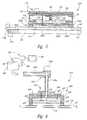
- FIG. 1schematically illustrates a CMP machine 10 with a platen 20 , a wafer carrier 30 , a polishing pad 27 , and a planarizing liquid 28 on the polishing pad 27 .
- the polishing pad 27may be a conventional polishing pad made from a continuous phase matrix material (e.g., polyurethane), or it may be a new generation fixed abrasive polishing pad made from abrasive particles fixedly dispersed in a suspension medium.
- the planarizing liquid 28may be a conventional CMP slurry with abrasive particles and chemicals that etch and/or oxidize the wafer, or the planarizing liquid 28 may be a planarizing solution without abrasive particles that contains only chemicals to etch and/or oxidize the surface of the wafer.
- conventional CMP slurriesare used on conventional polishing pads, and planarizing solutions without abrasive particles are used on fixed abrasive polishing pads.
- the CMP machine 10also has an underpad 25 attached to an upper surface 22 of the platen 20 and the lower surface of the polishing pad 27 .
- a drive assembly 26rotates the platen 20 as indicated by arrow A.
- the drive assembly 26reciprocates the platen 20 back and forth as indicated by arrow B. Since the polishing pad 27 is attached to the underpad 25 , the polishing pad 27 moves with the platen 20 .
- the wafer carrier 30has a lower surface 33 to which a wafer 12 may be attached, or the wafer 12 may be attached to a resilient pad 34 positioned between the wafer 12 and the lower surface 33 .
- the wafer carrier 30may be a weighted, free-floating wafer carrier, or an actuator assembly 40 may be attached to the wafer carrier to impart axial and/or rotational motion (indicated by arrows C and D, respectively).
- the wafer carrier 30presses the wafer 12 face-downward against the polishing pad 27 . While the face of the wafer 12 presses against the polishing pad 27 , at least one of the platen 20 or the wafer carrier 30 moves relative to the other to move the wafer 12 across the planarizing surface 29 . As the face of the wafer 12 moves across the planarizing surface 29 , the polishing pad 27 and the planarizing liquid 28 continually remove material from the face of the wafer 12 .
- CMP processesmust consistently and accurately produce a uniform, planar surface on the wafer to enable precise circuit and device patterns to be formed with photolithography techniques. As the density of integrated circuits increases, it is often necessary to accurately focus the critical dimensions of the photo-patterns to within a tolerance of approximately 0.1 ⁇ m. Focusing photo-patterns of such small tolerances, however, is difficult when the planarized surface of the wafer is not uniformly planar. Thus, CMP processes must create a highly uniform, planar surface.
- planarized surface of the wafermay not be sufficiently uniform across the whole surface of the wafer.
- the uniformity of the planarized surfaceis a function of several variables, including the pressure between the wafer and the planarizing surface, the temperature of the wafer and/or the planarizing surface, and the temperature and pH of the planarizing liquid.
- One conventional approach to addressing this problemhas been to measure some or all of the above variables and adjust the CMP processing conditions to improve the uniformity of the wafers. This approach has created additional problems. For example, if the measurements are made while the CMP machine is stationary, they may not be representative of the actual conditions present during planarization. On the other hand, if sensors are placed on the wafer carrier to make measurements during planarization, mechanical means, such as slip rings and the like may be required to transmit electrical signals from the moving sensors to a stationary display.
- remote sensing meansFor example, an infrared gun may be used to measure the temperature of the wafer during planarization. This approach suffers from several drawbacks.
- One drawbackis that the temperature readings obtained from the infrared gun may be distorted by the presence of the planarizing liquid.
- a second drawbackis that remote sensing means may not be readily available for some types of sensors, for example, pressure transducers. Accordingly, it may be difficult to determine the pressure between the wafer and the polishing pad during planarization.
- One conventional approach for obtaining in situ pressure measurementsis to place the pressure transducer on a mechanical linkage between the wafer carrier and a fixed reference point.
- This approachmay suffer from still further drawbacks.
- the weight of the mechanical linkagemay distort the pressure measurement, and the linkage itself may have such a high inertia that it is unable to respond quickly to sudden pressure changes.
- each approachmay require that a sensor and associated peripheral hardware be installed on a large number of CMP machines, although the planarizing characteristics may need to be monitored only periodically. As a result, the cost for sensors, peripheral hardware, and maintenance may be higher than is necessary.
- One factor that affects the throughput of CMP processingis the ability to accurately stop planarizing a given wafer or type of wafers at a desired endpoint.
- conventional CMP processestypically stop planarizing the wafer and measure the change in thickness of the wafer with an interferometer or other distance measuring device. If the wafer is under-planarized, CMP processing is resumed and the wafer is periodically measured until the wafer reaches its desired endpoint. If the wafer is over-planarized, the wafer may be partially or fully damaged.
- the throughput of finished wafersis accordingly greatly affected by the ability to accurately and quickly determine the endpoint of individual wafers and/or types of wafer.
- the present inventionis directed toward a method and apparatus for the wireless transfer of measurements made during chemical-mechanical planarization of a semiconductor substrate with a planarizing device.
- the planarizing devicemay have a support, a platen assembly connected to the support, and a carrier movable relative to the platen assembly and the support to remove material from a semiconductor substrate positioned between the carrier and the platen assembly.
- the apparatusmay comprise a sensor connected to the platen assembly, the carrier, or the semiconductor substrate. The sensor generates a signal corresponding to a value of a selected property of the planarizing device or the semiconductor substrate.
- the propertymay be a force exerted against the semiconductor substrate by the carrier, a temperature or resistance of the semiconductor substrate, or the pH of planarizing liquid surrounding the semiconductor substrate.
- the apparatusmay further include a display spaced apart from the sensor and a wireless communication link coupled between the sensor and the display to transmit the signal from the sensor to the display.
- the wireless communication linkmay include an infrared, radio, or acoustic transmitter and receiver, or a pair of inductors.
- the signalmay be transmitted in real time from the sensor to the display.
- the signalmay be stored and then transmitted in a batch manner, and the communication link may include a cable or the wireless means described above.
- the apparatusmay include a feedback loop that changes the selected property based on the signal generated by the sensor.
- the apparatusmay remove material from a substrate having a reflective layer and a transparent surface opposite the reflective layer.
- the apparatusmay include a light source positioned to illuminate the substrate, and a light sensor positioned to detect the presence or absence of light reflected from the reflective layer through the transparent surface of the substrate.
- the reflective layermay have a hardness approximately the same as the hardness of a semiconductor wafer so that removal of the reflective layer is representative of semiconductor wafer planarization.
- FIG. 1is a partial cross-sectional elevation view of a chemical-mechanical planarization machine in accordance with the prior art.
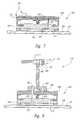
- FIG. 2is a partial cross-sectional elevation view of an apparatus in accordance with an embodiment of the present invention.
- FIG. 3is a top plan view of a portion of the apparatus shown in FIG. 2 .
- FIG. 4Ais a block diagram of a transmitter assembly and a receiver assembly in accordance with an embodiment of the invention.
- FIG. 4Bis a block diagram of a transmitter assembly and a receiver assembly in accordance with another embodiment of the invention.
- FIG. 5is a partial cross-sectional elevation view of a carrier assembly in accordance with another embodiment of the invention.
- FIG. 6is a partially schematic, partial cross-sectional elevation view of an apparatus in accordance with still another embodiment of the invention.
- FIG. 7is a partial cross-sectional elevation view of a carrier assembly in accordance with yet another embodiment of the invention.
- FIG. 8is a partial cross-sectional elevation view of a portion of an apparatus engaging a substrate in accordance with still another embodiment of the invention.
- FIG. 9is a top plan view of the substrate shown in FIG. 8 .
- FIG. 10is a partial cross-sectional elevation view of a carrier assembly in accordance with another embodiment of the invention.
- the present inventionis directed toward methods and apparatuses for transmitting data from a chemical-mechanical planarization machine.
- the apparatusmay include a wireless communication link to transmit the data from a movable portion of the machine to a fixed point.
- FIG. 2illustrates a CMP apparatus 110 for measuring the values of one or more parameters associated with chemical-mechanical planarization of a semiconductor substrate or wafer 112 .
- the apparatus 110has a platen 120 , an underpad 125 mounted to the top surface of the platen 120 , and a polishing pad 127 mounted to the top surface of the underpad 125 .
- the platen 120may be movable relative to a fixed support structure 114 by means of a drive assembly 126 that may impart rotational motion (indicated by arrow A) and/or translational motion (indicated by arrow B) to the platen 120 .
- the apparatus 110may also include a carrier assembly 130 that engages the semiconductor substrate 112 and moves the semiconductor substrate relative to the polishing pad 127 to remove material therefrom.
- a retainer ring 131prevents the semiconductor substrate 112 from sliding away from the carrier assembly 130 .
- the carrier assembly 130is supported relative to the polishing pad 127 by a horizontal support arm 143 and a vertical drive shaft 142 .
- the horizontal support arm 143may include outer and inner telescoping segments 143 a and 143 b .
- the outer telescoping segment 143 ais attached to the support structure 114
- the inner telescoping segment 143 bmay slide relative to the outer telescoping segment 143 a as indicated by arrow E, to oscillate the carrier assembly 130 in a horizontal direction.
- the inner telescoping segment 143 b and carrier assembly 130are driven by an actuator 140 a and a linkage 149 , and in other embodiments, other means oscillate the carrier assembly 130 .
- the drive shaft 142extends between the inner telescoping segment 143 b and the carrier assembly 130 .
- the drive shaft 142may be coupled to an actuator 140 b that imparts to the carrier assembly 130 a vertical motion, indicated by arrow C, and/or a rotational motion, indicated by arrow D.
- the driveshaft 142further includes a coupling member or plate 144 that has a plurality of vacuum apertures 148 to releasably engage the carrier assembly 130 .
- the vacuum apertures 148are coupled to a vacuum source (not shown) by a series of connecting conduits 145 (shown in FIG. 2 as 145 a , 145 b , and 145 c ) that pass through the drive shaft 142 and the support arm 143 .
- a rotational seal 146 at the junction between the support arm 143 and the drive shaft 142connects the rotating portion of the conduit 145 a to the translating portions of the conduit 145 b and 145 c.
- the carrier assembly 130includes a mounting member or plate 150 coupled to the coupling plate 144 and an engaging member or plate 132 that engages the semiconductor substrate 112 .
- the mounting plate 150has a smooth upper surface and an O-ring 154 to provide a gas-tight seal with the coupling plate 144 . When a vacuum is drawn through the vacuum apertures 148 by the vacuum source, the coupling plate 144 may fly engage the mounting plate 150 .
- the engaging plate 132is positioned beneath the mounting plate 150 and is coupled to the mounting plate 150 by a spacer ring 151 and a vertical coupling 193 .
- the spacer ring 151is attached to a lower surface of the mounting plate 150 and extends around the periphery of the mounting plate toward the engaging plate 132 .
- the spacer ring 151has a plurality of circular apertures 152 in a lower flange 156 thereof.
- Bolts 153extend through the apertures 152 and bear against the walls of the apertures to impart rotational motion from the drive shaft 142 to the engaging plate 132 .
- a force sensor 190is positioned between the vertical coupling 193 and the mounting plate 150 .
- the force sensor 190may be positioned in other portions of the apparatus 110 , so long as it is in the load path between the actuator 140 b and the semiconductor substrate 112 , and is sufficiently close to the semiconductor substrate 112 to accurately measure the vertical forces transmitted thereto.
- the force sensor 190may be one of a variety of commercially available transducers configured to measure steady state and/or variable forces and generate a corresponding electrical signal.
- a calibrator 194may be attached to the mounting plate 150 and coupled to the force sensor 190 to calibrate the electrical signal with a known value.
- the force sensor 190is connected to a transmitter assembly 170 that generates wireless signals corresponding to the force sensor signals.
- the wireless signalsare transmitted by a transmitter 177 to one or more transmitting transducers 175 and then to a receiver assembly 160 .
- the receiver assembly 160includes a receiving transducer 161 positioned to receive the wireless signals, and a receiver 165 coupled to the receiving transducer 161 .
- the receiver assembly 160is coupled to an electronic device 169 .
- the electronic device 169may include a display that displays the signals in a human readable format. In other embodiments, the electronic device 169 may include a chart recorder, printer, or other output device.
- FIG. 3is a top plan view of the mounting plate 150 and the transmitter assembly 170 shown in FIG. 2 .
- several transmitting transducers 175are coupled to the transmitter 177 with cables 192 routed through cable passages 155 in the mounting plate 150 . Accordingly, even where the signals emitted by the transmitting transducers 175 travel in generally straight lines, the signals emitted by at least one of the transmitting transducers 175 will be coupled to the receiving transducer 161 (FIG. 2) at all times.
- the transmitting transducers 175 and the receiving transducer 161may transmit wireless signals by one or more of several means.
- the transmitting transducers 175 and the receiving transducers 161may generate and receive, respectively, optic signals, such as infrared, ultraviolet, or visible light signals.
- the transmitting transducer 175can include a light source and a waveguide, such as a fiber optic cable, having an emission point from which optic signals are emitted.
- the transmitting transducer 175may include other types of waveguides.
- the transmitting transducers 175 and the receiving transducers 161may generate and receive, respectively, radio signals or acoustic signals, for example, subsonic, sonic, or ultrasonic signals.
- the transmitting transducers 175may include inductors that generate magnetic signals and the receiving transducer 161 may include a corresponding inductor to receive the magnetic signal.
- the transmitting transducers 175may be spaced apart from the receiving transducer 161 in each of the foregoing embodiments, and may be movable relative to the receiver assembly 160 without interrupting the flow of signals therebetween.
- the transmitter assembly 170may be attached to the mounting plate 150 .
- the transmitter assembly 170may be attached to any portion of the apparatus 110 that moves relative to the electronic device 169 , such as the platen 120 or the semiconductor substrate 112 .
- the receiving transducer 161may be positioned adjacent the support structure 114 , as shown in FIG. 2, or, as is also shown in FIG.
- a receiving transducer 161 amay be positioned on the platen 120 where the platen 120 does not move relative to the electronic device 169 .
- the receiving transducer 161may be positioned on any portion of the apparatus that is generally fixed relative to the electronic device 169 .
- the receiving transducer 161may include a parabolic horn to receive even relatively weak signals generated by the transmitting transducer 175 , reducing the power required by the transmitter 177 .
- FIG. 4Ais a schematic block diagram of a transmitter assembly 170 and receiver assembly 160 in accordance with an embodiment of the invention.
- the transmitter assembly 170is configured to transmit signals from several sensors 190 (shown as 190 a , 190 b , 190 c ) that may be calibrated with a corresponding plurality of calibrators 194 (shown as 194 a , 194 b , and 194 c ).
- Each sensor 190is coupled to a signal conditioner 171 (shown as 171 a , 171 b , and 171 c ) to reduce noise in the signals generated by the sensors 190 .
- the conditioned signalsare then transmitted to a multiplexer 172 , that samples each signal stream and compiles a single composite signal stream.
- the composite signal streamproceeds from the multiplexer 172 to a modulator 173 that modulates either the frequency or the amplitude of the signal stream.
- the modulator 173may be replaced with an A/D processor 174 , as shown in dashed lines in FIG. 4 A.
- the A/D processor 174may include a converter, a central processing unit or discrete logic device, a storage device and/or a control code unit, and transforms the analog signal from the multiplexer 172 to a bit stream which is then conveyed to the transmitting transducer 175 .
- the multiplexer 172 , A/D processor 174 , and transducer 175may comprise a commercially available unit, such as a Microstamp system available from Micron Technology, Inc. of Boise, Id., or a Strain LinkTM system available from Microstrain of Burlington, Vt.
- the transmitter assembly 170further includes a power supply 178 coupled to the sensors 190 , the signal conditioners 171 and any other components requiring power, such as the multiplexer 172 , the modulator 173 , and the A/D processor 174 .
- the power supply 178may include a battery.
- the power supplymay include a solar cell or other device that does not require external cable connections during planarization, for example, a first inductor that is magnetically or electromagnetically coupled to a corresponding second inductor to generate electrical current.
- the signal transmitted by the transmitting transducer 175is received by the receiving transducer 161 , as discussed above with reference to FIGS. 2 and 3.
- the receiving transducer 161is coupled to a demodulator 162 to convert the signal to a voltage, then to a demultiplexer 163 to separate individual signals from the signal stream, and then to a processor 164 a .
- the processor 164 amay convert the voltage to a human readable format where the electronic device 169 is a display.
- the demodulator 162 and demultiplexer 163are replaced by a processor 164 b , as shown in dashed lines in FIG. 4 A.
- Still another advantage of the apparatus 110 shown in FIGS. 2-3is that the carrier assembly 130 may be easily removed from the apparatus 110 and moved to another CMP machine.
- the receiver assembly 160 and electronic device 169may also be easily moved from one machine to another. Accordingly, the force sensor 190 may be used periodically to run diagnostic checks of individual CMP machines without the need to simultaneously outfit each machine with a complete transmitter assembly 170 and receiver assembly 160 .
- FIG. 4Bis a schematic block diagram of a receiver assembly 160 a and a transmitter assembly 170 a in accordance with another embodiment of the invention.
- the receiver assembly 160 ais generally similar to the receiver assembly shown in FIGS. 2-4A.
- the transmitter assembly 170 ais generally similar to the transmitter assembly 170 shown in FIGS. 2-4A; however, it further includes a storage or memory device 179 coupled to the multiplexer 172 .
- the storage device 179may be used to store data received from the sensors 190 and transmit the data to the transducer 175 in a batch format.
- the carrier assembly 130(FIG. 2) may be halted prior to conveying the data from the sensor 190 to the electronic device 169 .
- the transducers 175 and 161may be replaced by a cable 166 that is coupled between the transmitter assembly 170 a and the receiver assembly 160 a while the data is transmitted.
- the cable 166may be removed after the data has been transmitted and before resuming motion of the carrier assembly 130 .
- An advantage of the transmitter assembly 170 a shown in FIG. 4B when compared with the transmitter assembly 170 shown in FIG. 4Ais that it may eliminate the need for the transducers 175 and 161 .
- an advantage of the transmitter assembly 170 shown in FIG. 4Ais that it is configured to transmit real-time data rather than batch data.
- the pH sensors 390may include a conventional electronic pH meter such as is available from PGC Scientific of Gaithersburg, Md., or Beckman Instruments of Fullerton, Calif.
- one pH sensor 390 amay be attached to the carrier assembly 230 .
- another pH sensor 390 bmay be attached to the platen 120 , and may be coupled to a transmitter 177 b and transmitting transducer 175 b , also attached to the platen 120 .
- the carrier assembly 230 and/or the platen 120may include other sensors to measure the values of other parameters related to CMP processes, so long as the measurements may be converted to wireless signals.
- the temperature sensors 290 and the pH sensors 390 shown in FIG. 5may be used to obtain additional diagnostic data during the planarization process.
- the signals generated by the sensorsmay be transmitted in real-time, as is generally shown in FIG. 4A, or may be stored and transmitted in a batch fashion, as is shown in FIG. 4 B.
- Data from different types of sensorse.g., force, temperature, pH
- data from a plurality of sensors of the same typee.g., several force sensors
- FIG. 6is a cross-sectional elevation view of an apparatus 410 having an acoustic transmitting transducer 475 , such as an audio speaker, and an acoustic receiving transducer 461 , such as an audio microphone, in accordance with another embodiment of the invention.
- the carrier assembly 430includes a mounting member 450 removably attached with bolts 447 to the coupling plate 444 .
- the mounting member 450includes a cylinder 437 having cylinder walls 436 configured to slidably receive the engaging member 432 .
- the engaging member 432includes an O-ring 438 that sealably engages the cylinder walls 436 and is slidable within the cylinder 437 to press the semiconductor substrate 112 into engagement with the polishing pad 127 .
- the apparatus 410further includes a pressurized air source 480 coupled with conduits 445 a and 445 b to the cylinder 437 .
- the air pressure within the cylinder 437may be adjusted with the air source 480 to a desired level, thus establishing a desired force between the semiconductor substrate 112 and the polishing pad 127 .
- a pressure transducer 490is configured to measure the air pressure within the cylinder 437 and transmit the measurement to the transmitter assembly 170 and the acoustic transmitting transducer 475 .
- the acoustic signal emitted by the acoustic transmitting transducer 475is conveyed through the conduits 445 a and 445 b to the acoustic receiving transducer 461 positioned at the pressurized air source 480 .
- the acoustic receiving transducer 461is coupled to the receiver assembly 160 and the display 169 , generally as discussed above with reference to FIGS. 2-4B.
- the receiver assembly 160may also be coupled to the pressurized air source 480 to provide a feedback loop.
- the receiver assembly 160may be connected to an electronic feedback device 469 to automatically control the pressurized air source 480 , based on the signals received from the acoustic transmitting transducer 475 , and provide a selected pressure in the cylinder 437 .
- An advantage of the apparatus 410 shown in FIG. 6is that it may automatically adjust the force between the semiconductor substrate 112 and the polishing pad 127 based on measurements made by the pressure transducer 490 .
- similar feedback loopsmay be coupled to a heater to regulate the temperature of the semiconductor substrate 112 , or to a chemical dispenser to regulate the pH of the planarizing solution 128 on the polishing pad 127 .
- Another advantage of an embodiment of the invention shown in FIG. 6is that some existing planarizing machines may include the air source 480 and the cylinder 437 , allowing the wireless communication link to incorporate existing hardware.
- the light source 580generates visible light and the light detector 590 detects visible light. In other embodiments, the light source 580 and detector 590 operate at other wavelengths. In any case, signals generated by the detector 590 may be conveyed to the transmitter assembly 170 and then to the receiver assembly 160 (FIG. 2 ), as was discussed above with reference to FIGS. 2-4B.
- the transparent substrate 512may have dimensions generally similar to those of a conventional semiconductor substrate (such as a silicon substrate) and the reflective layer 513 may have a hardness that is representative of the surface of the conventional semiconductor substrate.
- the reflective layer 513may accordingly be removed at a rate similar to the rate at which material is removed from a conventional semiconductor wafer surface.
- the carrier assembly 530 and transparent substrate 512may be used to calibrate the apparatus 110 (FIG. 2) by simulating conditions under which an actual semiconductor substrate is planarized.
- FIG. 8is a cross-sectional elevation view of an apparatus 610 having a non-rotating light source 680 and light detector 690 in accordance with another embodiment of the invention.
- the light source 680 and the detector 690are positioned above the carrier assembly 630 .
- the coupling plate 644 , mounting plate 650 , and engaging plate 632are each provided with a plurality of apertures 635 to allow the light generated by the light source 680 to illuminate the substrate 612 and reflect from the reflective layer 613 upward to the detector 690 , as was discussed above with reference to FIG. 7 .
- FIG. 9is a top plan view of the substrate 612 shown in FIG. 8 .
- the reflective layer 613 on the surface of the substrate 612may include a plurality of radial segments 615 , each aligned with one or more of the apertures 635 (FIG. 8 ).
- an advantage of the apparatus 610 and substrate 612 shown in FIGS. 8 and 9is that the light detector 690 may detect light reflected from a variety of positions on the substrate 612 as the substrate rotates relative to the light detector. This is advantageous because it may indicate areas of the substrate 612 that planarize at different rates.
- FIG. 10is a partial cross-sectional elevation view of a carrier 730 and a substrate 712 in accordance with yet another embodiment of the invention.
- the substrate 712includes an electrically conductive layer 713 facing the polishing pad 127 .
- the conductive layer 713is connected with leads 792 to an ohm meter 790 that measures the resistance of the conductive layer 713 .
- the thickness of the conductive layer 713is gradually reduced, altering the resistance of the conductive layer.
- the change in resistanceis detected by the ohm meter 790 , and may be used to indicate when planarization is complete or when various planarizing parameters, such as temperature and pressure, are either too great, creating too high a rate of planarization, or too small, creating too low a rate of planarization.
- the conductive leads 792may connect to the planarized surface of the substrate 712 .
- the conductive leads 792may be coupled to vias that are integrally formed with the substrate 712 and that extend between the leads 792 and the conductive layer 713 .
- the conductive layer 713may include the outer surface of a conventional semiconductor substrate.
Landscapes
- Engineering & Computer Science (AREA)
- Mechanical Engineering (AREA)
- Manufacturing & Machinery (AREA)
- Computer Hardware Design (AREA)
- Microelectronics & Electronic Packaging (AREA)
- Power Engineering (AREA)
- Arrangements For Transmission Of Measured Signals (AREA)
- Mechanical Treatment Of Semiconductor (AREA)
- Finish Polishing, Edge Sharpening, And Grinding By Specific Grinding Devices (AREA)
- Force Measurement Appropriate To Specific Purposes (AREA)
Abstract
Description
Claims (28)
Priority Applications (1)
| Application Number | Priority Date | Filing Date | Title |
|---|---|---|---|
| US09/853,150US6626734B2 (en) | 1998-08-31 | 2001-05-09 | Method and apparatus for wireless transfer of chemical-mechanical planarization measurements |
Applications Claiming Priority (2)
| Application Number | Priority Date | Filing Date | Title |
|---|---|---|---|
| US09/144,756US6352466B1 (en) | 1998-08-31 | 1998-08-31 | Method and apparatus for wireless transfer of chemical-mechanical planarization measurements |
| US09/853,150US6626734B2 (en) | 1998-08-31 | 2001-05-09 | Method and apparatus for wireless transfer of chemical-mechanical planarization measurements |
Related Parent Applications (1)
| Application Number | Title | Priority Date | Filing Date |
|---|---|---|---|
| US09/144,756DivisionUS6352466B1 (en) | 1998-08-31 | 1998-08-31 | Method and apparatus for wireless transfer of chemical-mechanical planarization measurements |
Publications (2)
| Publication Number | Publication Date |
|---|---|
| US20010024930A1 US20010024930A1 (en) | 2001-09-27 |
| US6626734B2true US6626734B2 (en) | 2003-09-30 |
Family
ID=22509991
Family Applications (10)
| Application Number | Title | Priority Date | Filing Date |
|---|---|---|---|
| US09/144,756Expired - Fee RelatedUS6352466B1 (en) | 1998-08-31 | 1998-08-31 | Method and apparatus for wireless transfer of chemical-mechanical planarization measurements |
| US09/853,058Expired - Fee RelatedUS6547639B2 (en) | 1998-08-31 | 2001-05-09 | Method and apparatus for wireless transfer of chemical-mechanical planarization measurements |
| US09/853,150Expired - LifetimeUS6626734B2 (en) | 1998-08-31 | 2001-05-09 | Method and apparatus for wireless transfer of chemical-mechanical planarization measurements |
| US09/852,885Expired - LifetimeUS6702647B2 (en) | 1998-08-31 | 2001-05-09 | Method and apparatus for wireless transfer of chemical-mechanical planarization measurements |
| US09/853,067Expired - Fee RelatedUS6736698B2 (en) | 1998-08-31 | 2001-05-09 | Method and apparatus for wireless transfer of chemical-mechanical planarization measurements |
| US09/924,368Expired - Fee RelatedUS6827630B2 (en) | 1998-08-31 | 2001-08-07 | Method and apparatus for wireless transfer of chemical-mechanical planarization measurements |
| US09/924,063Expired - LifetimeUS6612900B2 (en) | 1998-08-31 | 2001-08-07 | Method and apparatus for wireless transfer of chemical-mechanical planarization measurements |
| US09/924,367Expired - Fee RelatedUS6780082B2 (en) | 1998-08-31 | 2001-08-07 | Method and apparatus for wireless transfer of chemical-mechanical planarization measurements |
| US09/924,362Expired - Fee RelatedUS6786799B2 (en) | 1998-08-31 | 2001-08-07 | Method and apparatus for wireless transfer of chemical-mechanical planarization measurements |
| US09/924,369Expired - Fee RelatedUS6540588B2 (en) | 1998-08-31 | 2001-08-07 | Method and apparatus for wireless transfer of chemical-mechanical planarization measurements |
Family Applications Before (2)
| Application Number | Title | Priority Date | Filing Date |
|---|---|---|---|
| US09/144,756Expired - Fee RelatedUS6352466B1 (en) | 1998-08-31 | 1998-08-31 | Method and apparatus for wireless transfer of chemical-mechanical planarization measurements |
| US09/853,058Expired - Fee RelatedUS6547639B2 (en) | 1998-08-31 | 2001-05-09 | Method and apparatus for wireless transfer of chemical-mechanical planarization measurements |
Family Applications After (7)
| Application Number | Title | Priority Date | Filing Date |
|---|---|---|---|
| US09/852,885Expired - LifetimeUS6702647B2 (en) | 1998-08-31 | 2001-05-09 | Method and apparatus for wireless transfer of chemical-mechanical planarization measurements |
| US09/853,067Expired - Fee RelatedUS6736698B2 (en) | 1998-08-31 | 2001-05-09 | Method and apparatus for wireless transfer of chemical-mechanical planarization measurements |
| US09/924,368Expired - Fee RelatedUS6827630B2 (en) | 1998-08-31 | 2001-08-07 | Method and apparatus for wireless transfer of chemical-mechanical planarization measurements |
| US09/924,063Expired - LifetimeUS6612900B2 (en) | 1998-08-31 | 2001-08-07 | Method and apparatus for wireless transfer of chemical-mechanical planarization measurements |
| US09/924,367Expired - Fee RelatedUS6780082B2 (en) | 1998-08-31 | 2001-08-07 | Method and apparatus for wireless transfer of chemical-mechanical planarization measurements |
| US09/924,362Expired - Fee RelatedUS6786799B2 (en) | 1998-08-31 | 2001-08-07 | Method and apparatus for wireless transfer of chemical-mechanical planarization measurements |
| US09/924,369Expired - Fee RelatedUS6540588B2 (en) | 1998-08-31 | 2001-08-07 | Method and apparatus for wireless transfer of chemical-mechanical planarization measurements |
Country Status (4)
| Country | Link |
|---|---|
| US (10) | US6352466B1 (en) |
| AU (1) | AU5903299A (en) |
| TW (1) | TW426581B (en) |
| WO (1) | WO2000012263A1 (en) |
Cited By (3)
| Publication number | Priority date | Publication date | Assignee | Title |
|---|---|---|---|---|
| US20030229468A1 (en)* | 2002-06-07 | 2003-12-11 | Nanya Technology Corporation | Chemical mechanical polishing apparatus having a measuring device for measuring a guide ring |
| US20080087069A1 (en)* | 2006-10-03 | 2008-04-17 | Sensarray Corporation | Pressure Sensing Device |
| US7722434B2 (en) | 2005-03-29 | 2010-05-25 | Kla-Tencor Corporation | Apparatus for measurement of parameters in process equipment |
Families Citing this family (120)
| Publication number | Priority date | Publication date | Assignee | Title |
|---|---|---|---|---|
| US6075606A (en) | 1996-02-16 | 2000-06-13 | Doan; Trung T. | Endpoint detector and method for measuring a change in wafer thickness in chemical-mechanical polishing of semiconductor wafers and other microelectronic substrates |
| US6244121B1 (en) | 1998-03-06 | 2001-06-12 | Applied Materials, Inc. | Sensor device for non-intrusive diagnosis of a semiconductor processing system |
| US6352466B1 (en)* | 1998-08-31 | 2002-03-05 | Micron Technology, Inc. | Method and apparatus for wireless transfer of chemical-mechanical planarization measurements |
| US6191037B1 (en) | 1998-09-03 | 2001-02-20 | Micron Technology, Inc. | Methods, apparatuses and substrate assembly structures for fabricating microelectronic components using mechanical and chemical-mechanical planarization processes |
| US7034660B2 (en)* | 1999-02-26 | 2006-04-25 | Sri International | Sensor devices for structural health monitoring |
| US6383934B1 (en) | 1999-09-02 | 2002-05-07 | Micron Technology, Inc. | Method and apparatus for chemical-mechanical planarization of microelectronic substrates with selected planarizing liquids |
| US6306768B1 (en) | 1999-11-17 | 2001-10-23 | Micron Technology, Inc. | Method for planarizing microelectronic substrates having apertures |
| US6498101B1 (en) | 2000-02-28 | 2002-12-24 | Micron Technology, Inc. | Planarizing pads, planarizing machines and methods for making and using planarizing pads in mechanical and chemical-mechanical planarization of microelectronic device substrate assemblies |
| US6313038B1 (en) | 2000-04-26 | 2001-11-06 | Micron Technology, Inc. | Method and apparatus for controlling chemical interactions during planarization of microelectronic substrates |
| US6387289B1 (en)* | 2000-05-04 | 2002-05-14 | Micron Technology, Inc. | Planarizing machines and methods for mechanical and/or chemical-mechanical planarization of microelectronic-device substrate assemblies |
| US6612901B1 (en)* | 2000-06-07 | 2003-09-02 | Micron Technology, Inc. | Apparatus for in-situ optical endpointing of web-format planarizing machines in mechanical or chemical-mechanical planarization of microelectronic-device substrate assemblies |
| US6520834B1 (en)* | 2000-08-09 | 2003-02-18 | Micron Technology, Inc. | Methods and apparatuses for analyzing and controlling performance parameters in mechanical and chemical-mechanical planarization of microelectronic substrates |
| US7127362B2 (en)* | 2000-08-22 | 2006-10-24 | Mundt Randall S | Process tolerant methods and apparatus for obtaining data |
| US6736869B1 (en) | 2000-08-28 | 2004-05-18 | Micron Technology, Inc. | Method for forming a planarizing pad for planarization of microelectronic substrates |
| US6838382B1 (en)* | 2000-08-28 | 2005-01-04 | Micron Technology, Inc. | Method and apparatus for forming a planarizing pad having a film and texture elements for planarization of microelectronic substrates |
| US6609947B1 (en)* | 2000-08-30 | 2003-08-26 | Micron Technology, Inc. | Planarizing machines and control systems for mechanical and/or chemical-mechanical planarization of micro electronic substrates |
| US6592443B1 (en)* | 2000-08-30 | 2003-07-15 | Micron Technology, Inc. | Method and apparatus for forming and using planarizing pads for mechanical and chemical-mechanical planarization of microelectronic substrates |
| US6652764B1 (en) | 2000-08-31 | 2003-11-25 | Micron Technology, Inc. | Methods and apparatuses for making and using planarizing pads for mechanical and chemical-mechanical planarization of microelectronic substrates |
| US6623329B1 (en)* | 2000-08-31 | 2003-09-23 | Micron Technology, Inc. | Method and apparatus for supporting a microelectronic substrate relative to a planarization pad |
| WO2002038336A1 (en)* | 2000-09-25 | 2002-05-16 | Center For Tribology, Inc. | A method and apparatus for controlled polishing |
| US6494765B2 (en)* | 2000-09-25 | 2002-12-17 | Center For Tribology, Inc. | Method and apparatus for controlled polishing |
| US6540587B1 (en) | 2000-10-13 | 2003-04-01 | Lam Research Corporation | Infrared end-point detection system |
| NL1017593C2 (en)* | 2001-03-14 | 2002-09-17 | Asm Int | Inspection system for process devices for treating substrates, as well as a sensor intended for such an inspection system and a method for inspecting process devices. |
| US6572441B2 (en)* | 2001-05-31 | 2003-06-03 | Momentum Technical Consulting, Inc. | Method of and apparatus for chemical-mechanical polishing |
| WO2002102475A1 (en)* | 2001-06-07 | 2002-12-27 | Rutgers, The State University Of New Jersey | Method and apparatus for analyzing a golf stroke |
| US6722943B2 (en) | 2001-08-24 | 2004-04-20 | Micron Technology, Inc. | Planarizing machines and methods for dispensing planarizing solutions in the processing of microelectronic workpieces |
| US6866566B2 (en) | 2001-08-24 | 2005-03-15 | Micron Technology, Inc. | Apparatus and method for conditioning a contact surface of a processing pad used in processing microelectronic workpieces |
| US6666749B2 (en) | 2001-08-30 | 2003-12-23 | Micron Technology, Inc. | Apparatus and method for enhanced processing of microelectronic workpieces |
| US6562185B2 (en)* | 2001-09-18 | 2003-05-13 | Advanced Micro Devices, Inc. | Wafer based temperature sensors for characterizing chemical mechanical polishing processes |
| US6770505B1 (en)* | 2001-09-21 | 2004-08-03 | Lsi Logic Corporation | Arrangement for measuring pressure on a semiconductor wafer and an associated method for fabricating a semiconductor wafer |
| TW535293B (en)* | 2001-10-03 | 2003-06-01 | Hannstar Display Corp | Structure of and method for producing double vertical channel thin film transistor (DVC TFT) CMOS |
| US6736720B2 (en)* | 2001-12-26 | 2004-05-18 | Lam Research Corporation | Apparatus and methods for controlling wafer temperature in chemical mechanical polishing |
| US6712670B2 (en)* | 2001-12-27 | 2004-03-30 | Lam Research Corporation | Method and apparatus for applying downward force on wafer during CMP |
| US20030188829A1 (en)* | 2001-12-27 | 2003-10-09 | Bharath Rangarajan | Integrated pressure sensor for measuring multiaxis pressure gradients |
| US6939198B1 (en)* | 2001-12-28 | 2005-09-06 | Applied Materials, Inc. | Polishing system with in-line and in-situ metrology |
| US20050233770A1 (en)* | 2002-02-06 | 2005-10-20 | Ramsey Craig C | Wireless substrate-like sensor |
| US20050224899A1 (en)* | 2002-02-06 | 2005-10-13 | Ramsey Craig C | Wireless substrate-like sensor |
| US7289230B2 (en) | 2002-02-06 | 2007-10-30 | Cyberoptics Semiconductors, Inc. | Wireless substrate-like sensor |
| US20050092246A1 (en)* | 2002-02-22 | 2005-05-05 | Peter Baumann | Device for depositing thin layers with a wireless detection of process parameters |
| US7131889B1 (en)* | 2002-03-04 | 2006-11-07 | Micron Technology, Inc. | Method for planarizing microelectronic workpieces |
| US20030199112A1 (en)* | 2002-03-22 | 2003-10-23 | Applied Materials, Inc. | Copper wiring module control |
| US7233841B2 (en)* | 2002-04-19 | 2007-06-19 | Applied Materials, Inc. | Vision system |
| US7085622B2 (en)* | 2002-04-19 | 2006-08-01 | Applied Material, Inc. | Vision system |
| TWI261661B (en)* | 2002-06-21 | 2006-09-11 | Applied Materials Inc | Angled sensors for detecting substrates |
| US6869335B2 (en) | 2002-07-08 | 2005-03-22 | Micron Technology, Inc. | Retaining rings, planarizing apparatuses including retaining rings, and methods for planarizing micro-device workpieces |
| US7341502B2 (en) | 2002-07-18 | 2008-03-11 | Micron Technology, Inc. | Methods and systems for planarizing workpieces, e.g., microelectronic workpieces |
| US6860798B2 (en)* | 2002-08-08 | 2005-03-01 | Micron Technology, Inc. | Carrier assemblies, planarizing apparatuses including carrier assemblies, and methods for planarizing micro-device workpieces |
| US6884144B2 (en)* | 2002-08-16 | 2005-04-26 | Micron Technology, Inc. | Methods and systems for planarizing microelectronic devices with Ge-Se-Ag layers |
| US7094695B2 (en)* | 2002-08-21 | 2006-08-22 | Micron Technology, Inc. | Apparatus and method for conditioning a polishing pad used for mechanical and/or chemical-mechanical planarization |
| US7004817B2 (en) | 2002-08-23 | 2006-02-28 | Micron Technology, Inc. | Carrier assemblies, planarizing apparatuses including carrier assemblies, and methods for planarizing micro-device workpieces |
| US7011566B2 (en)* | 2002-08-26 | 2006-03-14 | Micron Technology, Inc. | Methods and systems for conditioning planarizing pads used in planarizing substrates |
| US6841991B2 (en) | 2002-08-29 | 2005-01-11 | Micron Technology, Inc. | Planarity diagnostic system, E.G., for microelectronic component test systems |
| US7008299B2 (en)* | 2002-08-29 | 2006-03-07 | Micron Technology, Inc. | Apparatus and method for mechanical and/or chemical-mechanical planarization of micro-device workpieces |
| US7440735B2 (en)* | 2002-10-23 | 2008-10-21 | Rosemount Inc. | Virtual wireless transmitter |
| JP3916549B2 (en)* | 2002-10-31 | 2007-05-16 | 東京エレクトロン株式会社 | Process monitor and semiconductor manufacturing apparatus |
| JP2004207687A (en)* | 2002-12-10 | 2004-07-22 | Sharp Corp | Semiconductor manufacturing apparatus and semiconductor manufacturing method using the same |
| US20040126906A1 (en)* | 2002-12-31 | 2004-07-01 | Tokyo Electron Limited | Method and apparatus for monitoring a material processing system |
| US20040127031A1 (en)* | 2002-12-31 | 2004-07-01 | Tokyo Electron Limited | Method and apparatus for monitoring a plasma in a material processing system |
| US7074114B2 (en) | 2003-01-16 | 2006-07-11 | Micron Technology, Inc. | Carrier assemblies, polishing machines including carrier assemblies, and methods for polishing micro-device workpieces |
| US6884152B2 (en)* | 2003-02-11 | 2005-04-26 | Micron Technology, Inc. | Apparatuses and methods for conditioning polishing pads used in polishing micro-device workpieces |
| US6872132B2 (en) | 2003-03-03 | 2005-03-29 | Micron Technology, Inc. | Systems and methods for monitoring characteristics of a polishing pad used in polishing micro-device workpieces |
| US6935929B2 (en) | 2003-04-28 | 2005-08-30 | Micron Technology, Inc. | Polishing machines including under-pads and methods for mechanical and/or chemical-mechanical polishing of microfeature workpieces |
| US7131891B2 (en)* | 2003-04-28 | 2006-11-07 | Micron Technology, Inc. | Systems and methods for mechanical and/or chemical-mechanical polishing of microfeature workpieces |
| US7471846B2 (en)* | 2003-06-26 | 2008-12-30 | Fotonation Vision Limited | Perfecting the effect of flash within an image acquisition devices using face detection |
| KR100669644B1 (en)* | 2003-08-02 | 2007-01-15 | 동부일렉트로닉스 주식회사 | Chemical mechanical polishing apparatus and method |
| US7030603B2 (en)* | 2003-08-21 | 2006-04-18 | Micron Technology, Inc. | Apparatuses and methods for monitoring rotation of a conductive microfeature workpiece |
| US20050197048A1 (en)* | 2004-03-04 | 2005-09-08 | Leping Li | Method for manufacturing a workpiece and torque transducer module |
| US7086927B2 (en)* | 2004-03-09 | 2006-08-08 | Micron Technology, Inc. | Methods and systems for planarizing workpieces, e.g., microelectronic workpieces |
| JP2005288664A (en)* | 2004-04-05 | 2005-10-20 | Ebara Corp | Polishing device and method for detecting completion of polishing pad standing |
| US7066792B2 (en)* | 2004-08-06 | 2006-06-27 | Micron Technology, Inc. | Shaped polishing pads for beveling microfeature workpiece edges, and associate system and methods |
| US7033253B2 (en)* | 2004-08-12 | 2006-04-25 | Micron Technology, Inc. | Polishing pad conditioners having abrasives and brush elements, and associated systems and methods |
| US20060154569A1 (en)* | 2005-01-11 | 2006-07-13 | Terry Doyle | Platen assembly utilizing magnetic slip ring |
| US20060234398A1 (en)* | 2005-04-15 | 2006-10-19 | International Business Machines Corporation | Single ic-chip design on wafer with an embedded sensor utilizing rf capabilities to enable real-time data transmission |
| US7264539B2 (en)* | 2005-07-13 | 2007-09-04 | Micron Technology, Inc. | Systems and methods for removing microfeature workpiece surface defects |
| WO2007018391A1 (en)* | 2005-08-05 | 2007-02-15 | Seung-Hun Bae | Chemical mechanical polishing apparatus |
| US7438626B2 (en) | 2005-08-31 | 2008-10-21 | Micron Technology, Inc. | Apparatus and method for removing material from microfeature workpieces |
| US7326105B2 (en) | 2005-08-31 | 2008-02-05 | Micron Technology, Inc. | Retaining rings, and associated planarizing apparatuses, and related methods for planarizing micro-device workpieces |
| US7294049B2 (en)* | 2005-09-01 | 2007-11-13 | Micron Technology, Inc. | Method and apparatus for removing material from microfeature workpieces |
| US7893697B2 (en)* | 2006-02-21 | 2011-02-22 | Cyberoptics Semiconductor, Inc. | Capacitive distance sensing in semiconductor processing tools |
| US7804306B2 (en) | 2006-02-21 | 2010-09-28 | CyterOptics Semiconductor, Inc. | Capacitive distance sensing in semiconductor processing tools |
| US7537511B2 (en)* | 2006-03-14 | 2009-05-26 | Micron Technology, Inc. | Embedded fiber acoustic sensor for CMP process endpoint |
| US20070235133A1 (en)* | 2006-03-29 | 2007-10-11 | Strasbaugh | Devices and methods for measuring wafer characteristics during semiconductor wafer polishing |
| JP4814677B2 (en)* | 2006-03-31 | 2011-11-16 | 株式会社荏原製作所 | Substrate holding device and polishing device |
| US7840305B2 (en)* | 2006-06-28 | 2010-11-23 | 3M Innovative Properties Company | Abrasive articles, CMP monitoring system and method |
| WO2008019050A1 (en)* | 2006-08-03 | 2008-02-14 | Saint-Gobain Abrasives, Inc. | System and method for improved hand tool operation |
| EP1894900A3 (en)* | 2006-08-28 | 2010-02-24 | Osaka University | Catalyst-aided chemical processing method and apparatus |
| GB2455006A (en)* | 2006-09-29 | 2009-05-27 | Cyberoptics Semiconductor Inc | Substrate-like particle sensor |
| US7778793B2 (en)* | 2007-03-12 | 2010-08-17 | Cyberoptics Semiconductor, Inc. | Wireless sensor for semiconductor processing systems |
| US7754612B2 (en) | 2007-03-14 | 2010-07-13 | Micron Technology, Inc. | Methods and apparatuses for removing polysilicon from semiconductor workpieces |
| US20080246493A1 (en)* | 2007-04-05 | 2008-10-09 | Gardner Delrae H | Semiconductor Processing System With Integrated Showerhead Distance Measuring Device |
| US7476144B2 (en)* | 2007-06-13 | 2009-01-13 | Black & Decker Inc. | Sander |
| US7722435B2 (en)* | 2007-06-13 | 2010-05-25 | Black & Decker Inc. | Sander |
| US7485026B2 (en)* | 2007-06-13 | 2009-02-03 | Black & Decker Inc. | Sander |
| US7534165B2 (en)* | 2007-06-13 | 2009-05-19 | Black & Decker Inc. | Sander |
| US20090015268A1 (en)* | 2007-07-13 | 2009-01-15 | Gardner Delrae H | Device and method for compensating a capacitive sensor measurement for variations caused by environmental conditions in a semiconductor processing environment |
| US8556912B2 (en) | 2007-10-30 | 2013-10-15 | DePuy Synthes Products, LLC | Taper disengagement tool |
| TWM347669U (en)* | 2008-06-19 | 2008-12-21 | Bestac Advanced Material Co Ltd | Polishing pad and polishing device |
| US8182312B2 (en)* | 2008-09-06 | 2012-05-22 | Strasbaugh | CMP system with wireless endpoint detection system |
| KR101004435B1 (en)* | 2008-11-28 | 2010-12-28 | 세메스 주식회사 | Substrate Polishing Apparatus and Substrate Polishing Method Using The Same |
| KR101170760B1 (en)* | 2009-07-24 | 2012-08-03 | 세메스 주식회사 | Substrate polishing apparatus |
| US8533921B2 (en) | 2010-06-15 | 2013-09-17 | DePuy Synthes Products, LLC | Spiral assembly tool |
| US9095452B2 (en) | 2010-09-01 | 2015-08-04 | DePuy Synthes Products, Inc. | Disassembly tool |
| DE112011104610B4 (en) | 2010-12-27 | 2020-03-26 | Sumco Corporation | Method and device for polishing a workpiece |
| US9418904B2 (en) | 2011-11-14 | 2016-08-16 | Taiwan Semiconductor Manufacturing Co., Ltd. | Localized CMP to improve wafer planarization |
| US10065288B2 (en) | 2012-02-14 | 2018-09-04 | Taiwan Semiconductor Manufacturing Co., Ltd. | Chemical mechanical polishing (CMP) platform for local profile control |
| US20130210173A1 (en)* | 2012-02-14 | 2013-08-15 | Taiwan Semiconductor Manufacturing Co., Ltd. | Multiple Zone Temperature Control for CMP |
| US20130217306A1 (en)* | 2012-02-16 | 2013-08-22 | Taiwan Semiconductor Manufacturing Co., Ltd. | CMP Groove Depth and Conditioning Disk Monitoring |
| US9810679B2 (en)* | 2014-04-02 | 2017-11-07 | Colorado School Of Mines | Intelligent pad foot soil compaction devices and methods of using same |
| US9368941B1 (en)* | 2014-08-14 | 2016-06-14 | Google Inc. | Temperature compensation in an optical transmitter |
| CN106926112A (en)* | 2017-04-28 | 2017-07-07 | 青岛鑫嘉星电子科技股份有限公司 | A kind of the cut control system and control method of Sapphire Substrate polishing |
| US11565365B2 (en)* | 2017-11-13 | 2023-01-31 | Taiwan Semiconductor Manufacturing Co., Ltd. | System and method for monitoring chemical mechanical polishing |
| JP7045861B2 (en)* | 2018-01-17 | 2022-04-01 | 株式会社ディスコ | Support base |
| IT201800008047A1 (en)* | 2018-08-10 | 2020-02-10 | Mole Abrasivi Ermoli Srl | GRINDING SYSTEM INCLUDING A GRINDER AND A WHEEL AND METHOD TO EXCHANGE INFORMATION BETWEEN GRINDER AND WHEEL |
| IT201800008045A1 (en)* | 2018-08-10 | 2020-02-10 | Mole Abrasivi Ermoli Srl | GRINDING SYSTEM INCLUDING A WHEEL AND A GRINDING MACHINE WITH MOBILE DATA TRANSMISSION SYSTEM |
| CN109676452A (en)* | 2019-01-30 | 2019-04-26 | 哈尔滨理工大学 | Cylindrical grinder and control method based on portable mobile wireless control system |
| US11282755B2 (en) | 2019-08-27 | 2022-03-22 | Applied Materials, Inc. | Asymmetry correction via oriented wafer loading |
| AU2021105202A4 (en)* | 2021-06-18 | 2021-10-07 | Talene Hanna | Adhesive breast covers |
| JP7659490B2 (en)* | 2021-12-22 | 2025-04-09 | 株式会社荏原製作所 | How to calibrate an acoustic sensor |
| US20230411227A1 (en)* | 2022-06-17 | 2023-12-21 | Taiwan Semiconductor Manufacturing Company, Ltd. | Semiconductor processing tool and methods of operation |
| CN115213811B (en)* | 2022-07-20 | 2023-07-28 | 华侨大学 | Carrier for light-assisted chemical mechanical polishing and polishing processing method |
Citations (17)
| Publication number | Priority date | Publication date | Assignee | Title |
|---|---|---|---|---|
| EP0408015A2 (en) | 1989-07-13 | 1991-01-16 | Dainippon Screen Mfg. Co., Ltd. | Method of measuring thickness of film |
| US5240552A (en) | 1991-12-11 | 1993-08-31 | Micron Technology, Inc. | Chemical mechanical planarization (CMP) of a semiconductor wafer using acoustical waves for in-situ end point detection |
| US5413941A (en) | 1994-01-06 | 1995-05-09 | Micron Technology, Inc. | Optical end point detection methods in semiconductor planarizing polishing processes |
| EP0739687A2 (en) | 1995-04-26 | 1996-10-30 | Fujitsu Limited | Polishing apparatus and polishing method |
| US5685766A (en) | 1995-11-30 | 1997-11-11 | Speedfam Corporation | Polishing control method |
| WO1998005066A2 (en) | 1996-07-26 | 1998-02-05 | Speedfam Corporation | Methods and apparatus for the in-process detection and measurement of thin film layers |
| US5762537A (en) | 1993-08-25 | 1998-06-09 | Micron Technology, Inc. | System for real-time control of semiconductor wafer polishing including heater |
| US5877088A (en) | 1995-11-10 | 1999-03-02 | Nippon Steel Corporation | Flattening method and apparatus for semiconductor device |
| US5876265A (en) | 1995-04-26 | 1999-03-02 | Fujitsu Limited | End point polishing apparatus and polishing method |
| US5882244A (en) | 1995-07-20 | 1999-03-16 | Ebara Corporation | Polishing apparatus |
| US5951368A (en) | 1996-05-29 | 1999-09-14 | Ebara Corporation | Polishing apparatus |
| US6007408A (en) | 1997-08-21 | 1999-12-28 | Micron Technology, Inc. | Method and apparatus for endpointing mechanical and chemical-mechanical polishing of substrates |
| US6010538A (en) | 1996-01-11 | 2000-01-04 | Luxtron Corporation | In situ technique for monitoring and controlling a process of chemical-mechanical-polishing via a radiative communication link |
| US6042454A (en) | 1997-06-04 | 2000-03-28 | Ebara Corporation | System for detecting the endpoint of the polishing of a semiconductor wafer by a semiconductor wafer polisher |
| US6077151A (en) | 1999-05-17 | 2000-06-20 | Vlsi Technology, Inc. | Temperature control carrier head for chemical mechanical polishing process |
| US6095898A (en) | 1997-10-30 | 2000-08-01 | Wacker Siltronic Gesellschaft Fur Halbleitermaterialien Ag | Process and device for polishing semiconductor wafers |
| US6352466B1 (en)* | 1998-08-31 | 2002-03-05 | Micron Technology, Inc. | Method and apparatus for wireless transfer of chemical-mechanical planarization measurements |
Family Cites Families (14)
| Publication number | Priority date | Publication date | Assignee | Title |
|---|---|---|---|---|
| US4500881A (en) | 1982-09-23 | 1985-02-19 | Liquidometer Corporation | Inductively-coupled signalling system |
| US4561443A (en) | 1983-03-08 | 1985-12-31 | The Johns Hopkins University | Coherent inductive communications link for biomedical applications |
| US5213655A (en) | 1990-05-16 | 1993-05-25 | International Business Machines Corporation | Device and method for detecting an end point in polishing operation |
| US5499733A (en) | 1992-09-17 | 1996-03-19 | Luxtron Corporation | Optical techniques of measuring endpoint during the processing of material layers in an optically hostile environment |
| US5562529A (en) | 1992-10-08 | 1996-10-08 | Fujitsu Limited | Apparatus and method for uniformly polishing a wafer |
| US5891352A (en) | 1993-09-16 | 1999-04-06 | Luxtron Corporation | Optical techniques of measuring endpoint during the processing of material layers in an optically hostile environment |
| US5433651A (en) | 1993-12-22 | 1995-07-18 | International Business Machines Corporation | In-situ endpoint detection and process monitoring method and apparatus for chemical-mechanical polishing |
| US5791969A (en) | 1994-11-01 | 1998-08-11 | Lund; Douglas E. | System and method of automatically polishing semiconductor wafers |
| US5964643A (en)* | 1995-03-28 | 1999-10-12 | Applied Materials, Inc. | Apparatus and method for in-situ monitoring of chemical mechanical polishing operations |
| JP3471520B2 (en) | 1996-04-30 | 2003-12-02 | 富士通株式会社 | Method of manufacturing magnetoresistive head and method of manufacturing magnetoresistive head |
| US5643050A (en) | 1996-05-23 | 1997-07-01 | Industrial Technology Research Institute | Chemical/mechanical polish (CMP) thickness monitor |
| JPH10166262A (en) | 1996-12-10 | 1998-06-23 | Nikon Corp | Polishing equipment |
| US5873769A (en) | 1997-05-30 | 1999-02-23 | Industrial Technology Research Institute | Temperature compensated chemical mechanical polishing to achieve uniform removal rates |
| US5961368A (en)* | 1998-06-29 | 1999-10-05 | Chu; Yu-Po | Differential structure of remotely controlled toy car |
- 1998
- 1998-08-31USUS09/144,756patent/US6352466B1/ennot_activeExpired - Fee Related
- 1999
- 1999-08-30AUAU59032/99Apatent/AU5903299A/ennot_activeAbandoned
- 1999-08-30TWTW088114832Apatent/TW426581B/ennot_activeIP Right Cessation
- 1999-08-30WOPCT/US1999/019710patent/WO2000012263A1/enactiveApplication Filing
- 2001
- 2001-05-09USUS09/853,058patent/US6547639B2/ennot_activeExpired - Fee Related
- 2001-05-09USUS09/853,150patent/US6626734B2/ennot_activeExpired - Lifetime
- 2001-05-09USUS09/852,885patent/US6702647B2/ennot_activeExpired - Lifetime
- 2001-05-09USUS09/853,067patent/US6736698B2/ennot_activeExpired - Fee Related
- 2001-08-07USUS09/924,368patent/US6827630B2/ennot_activeExpired - Fee Related
- 2001-08-07USUS09/924,063patent/US6612900B2/ennot_activeExpired - Lifetime
- 2001-08-07USUS09/924,367patent/US6780082B2/ennot_activeExpired - Fee Related
- 2001-08-07USUS09/924,362patent/US6786799B2/ennot_activeExpired - Fee Related
- 2001-08-07USUS09/924,369patent/US6540588B2/ennot_activeExpired - Fee Related
Patent Citations (17)
| Publication number | Priority date | Publication date | Assignee | Title |
|---|---|---|---|---|
| EP0408015A2 (en) | 1989-07-13 | 1991-01-16 | Dainippon Screen Mfg. Co., Ltd. | Method of measuring thickness of film |
| US5240552A (en) | 1991-12-11 | 1993-08-31 | Micron Technology, Inc. | Chemical mechanical planarization (CMP) of a semiconductor wafer using acoustical waves for in-situ end point detection |
| US5762537A (en) | 1993-08-25 | 1998-06-09 | Micron Technology, Inc. | System for real-time control of semiconductor wafer polishing including heater |
| US5413941A (en) | 1994-01-06 | 1995-05-09 | Micron Technology, Inc. | Optical end point detection methods in semiconductor planarizing polishing processes |
| US5876265A (en) | 1995-04-26 | 1999-03-02 | Fujitsu Limited | End point polishing apparatus and polishing method |
| EP0739687A2 (en) | 1995-04-26 | 1996-10-30 | Fujitsu Limited | Polishing apparatus and polishing method |
| US5882244A (en) | 1995-07-20 | 1999-03-16 | Ebara Corporation | Polishing apparatus |
| US5877088A (en) | 1995-11-10 | 1999-03-02 | Nippon Steel Corporation | Flattening method and apparatus for semiconductor device |
| US5685766A (en) | 1995-11-30 | 1997-11-11 | Speedfam Corporation | Polishing control method |
| US6010538A (en) | 1996-01-11 | 2000-01-04 | Luxtron Corporation | In situ technique for monitoring and controlling a process of chemical-mechanical-polishing via a radiative communication link |
| US5951368A (en) | 1996-05-29 | 1999-09-14 | Ebara Corporation | Polishing apparatus |
| WO1998005066A2 (en) | 1996-07-26 | 1998-02-05 | Speedfam Corporation | Methods and apparatus for the in-process detection and measurement of thin film layers |
| US6042454A (en) | 1997-06-04 | 2000-03-28 | Ebara Corporation | System for detecting the endpoint of the polishing of a semiconductor wafer by a semiconductor wafer polisher |
| US6007408A (en) | 1997-08-21 | 1999-12-28 | Micron Technology, Inc. | Method and apparatus for endpointing mechanical and chemical-mechanical polishing of substrates |
| US6095898A (en) | 1997-10-30 | 2000-08-01 | Wacker Siltronic Gesellschaft Fur Halbleitermaterialien Ag | Process and device for polishing semiconductor wafers |
| US6352466B1 (en)* | 1998-08-31 | 2002-03-05 | Micron Technology, Inc. | Method and apparatus for wireless transfer of chemical-mechanical planarization measurements |
| US6077151A (en) | 1999-05-17 | 2000-06-20 | Vlsi Technology, Inc. | Temperature control carrier head for chemical mechanical polishing process |
Non-Patent Citations (2)
| Title |
|---|
| Brochure; StrainLink; "Multichannel Strain Transmitter," Description and drawings. |
| Internet Home Page for MicroStrain-www.microstrain.com. |
Cited By (5)
| Publication number | Priority date | Publication date | Assignee | Title |
|---|---|---|---|---|
| US20030229468A1 (en)* | 2002-06-07 | 2003-12-11 | Nanya Technology Corporation | Chemical mechanical polishing apparatus having a measuring device for measuring a guide ring |
| US6923709B2 (en)* | 2002-06-07 | 2005-08-02 | Nanya Technology Corporation | Chemical mechanical polishing apparatus having a measuring device for measuring a guide ring |
| US7722434B2 (en) | 2005-03-29 | 2010-05-25 | Kla-Tencor Corporation | Apparatus for measurement of parameters in process equipment |
| US20080087069A1 (en)* | 2006-10-03 | 2008-04-17 | Sensarray Corporation | Pressure Sensing Device |
| US7698952B2 (en) | 2006-10-03 | 2010-04-20 | Kla-Tencor Corporation | Pressure sensing device |
Also Published As
| Publication number | Publication date |
|---|---|
| US20010024930A1 (en) | 2001-09-27 |
| US6612900B2 (en) | 2003-09-02 |
| US20010024929A1 (en) | 2001-09-27 |
| US6827630B2 (en) | 2004-12-07 |
| US20010021621A1 (en) | 2001-09-13 |
| TW426581B (en) | 2001-03-21 |
| US6786799B2 (en) | 2004-09-07 |
| US20010049252A1 (en) | 2001-12-06 |
| WO2000012263A1 (en) | 2000-03-09 |
| US6547639B2 (en) | 2003-04-15 |
| US20010055932A1 (en) | 2001-12-27 |
| US6352466B1 (en) | 2002-03-05 |
| AU5903299A (en) | 2000-03-21 |
| US6736698B2 (en) | 2004-05-18 |
| US20020019194A1 (en) | 2002-02-14 |
| US20020002024A1 (en) | 2002-01-03 |
| US20010029152A1 (en) | 2001-10-11 |
| US6540588B2 (en) | 2003-04-01 |
| US6780082B2 (en) | 2004-08-24 |
| US20020028629A1 (en) | 2002-03-07 |
| US6702647B2 (en) | 2004-03-09 |
Similar Documents
| Publication | Publication Date | Title |
|---|---|---|
| US6626734B2 (en) | Method and apparatus for wireless transfer of chemical-mechanical planarization measurements | |
| US6464564B2 (en) | System for real-time control of semiconductor wafer polishing | |
| US20200269381A1 (en) | Polishing apparatus | |
| US6614529B1 (en) | In-situ real-time monitoring technique and apparatus for endpoint detection of thin films during chemical/mechanical polishing planarization | |
| US20070235133A1 (en) | Devices and methods for measuring wafer characteristics during semiconductor wafer polishing | |
| US7537511B2 (en) | Embedded fiber acoustic sensor for CMP process endpoint | |
| US20050054268A1 (en) | Methods for detecting transitions of wafer surface properties in chemical mechanical polishing for process status and control | |
| US9399276B2 (en) | Polishing apparatus | |
| JP2004503925A (en) | Polishing pad with built-in optical sensor | |
| CN101479075A (en) | Abrasive articles, CMP monitoring system and method | |
| KR19990044998A (en) | Method and apparatus for monitoring wear of polishing pads during polishing process | |
| US20080060758A1 (en) | Apparatus for detection of thin films during chemical/mechanical polishing planarization | |
| WO2021029264A1 (en) | End point detecting device and end point detecting method | |
| WO1995018353A1 (en) | Method and apparatus for monitoring thin films | |
| US6042454A (en) | System for detecting the endpoint of the polishing of a semiconductor wafer by a semiconductor wafer polisher | |
| US7549909B2 (en) | Methods for optical endpoint detection during semiconductor wafer polishing | |
| CN222553229U (en) | Polishing pad dresser and chemical mechanical polishing equipment | |
| GB2380960A (en) | Wafer polishing apparatus | |
| JP2001284301A (en) | Method and device monitoring thin film |
Legal Events
| Date | Code | Title | Description |
|---|---|---|---|
| STCF | Information on status: patent grant | Free format text:PATENTED CASE | |
| FEPP | Fee payment procedure | Free format text:PAYOR NUMBER ASSIGNED (ORIGINAL EVENT CODE: ASPN); ENTITY STATUS OF PATENT OWNER: LARGE ENTITY | |
| CC | Certificate of correction | ||
| FPAY | Fee payment | Year of fee payment:4 | |
| FPAY | Fee payment | Year of fee payment:8 | |
| FPAY | Fee payment | Year of fee payment:12 | |
| AS | Assignment | Owner name:U.S. BANK NATIONAL ASSOCIATION, AS COLLATERAL AGENT, CALIFORNIA Free format text:SECURITY INTEREST;ASSIGNOR:MICRON TECHNOLOGY, INC.;REEL/FRAME:038669/0001 Effective date:20160426 Owner name:U.S. BANK NATIONAL ASSOCIATION, AS COLLATERAL AGEN Free format text:SECURITY INTEREST;ASSIGNOR:MICRON TECHNOLOGY, INC.;REEL/FRAME:038669/0001 Effective date:20160426 | |
| AS | Assignment | Owner name:MORGAN STANLEY SENIOR FUNDING, INC., AS COLLATERAL AGENT, MARYLAND Free format text:PATENT SECURITY AGREEMENT;ASSIGNOR:MICRON TECHNOLOGY, INC.;REEL/FRAME:038954/0001 Effective date:20160426 Owner name:MORGAN STANLEY SENIOR FUNDING, INC., AS COLLATERAL Free format text:PATENT SECURITY AGREEMENT;ASSIGNOR:MICRON TECHNOLOGY, INC.;REEL/FRAME:038954/0001 Effective date:20160426 | |
| AS | Assignment | Owner name:U.S. BANK NATIONAL ASSOCIATION, AS COLLATERAL AGENT, CALIFORNIA Free format text:CORRECTIVE ASSIGNMENT TO CORRECT THE REPLACE ERRONEOUSLY FILED PATENT #7358718 WITH THE CORRECT PATENT #7358178 PREVIOUSLY RECORDED ON REEL 038669 FRAME 0001. ASSIGNOR(S) HEREBY CONFIRMS THE SECURITY INTEREST;ASSIGNOR:MICRON TECHNOLOGY, INC.;REEL/FRAME:043079/0001 Effective date:20160426 Owner name:U.S. BANK NATIONAL ASSOCIATION, AS COLLATERAL AGEN Free format text:CORRECTIVE ASSIGNMENT TO CORRECT THE REPLACE ERRONEOUSLY FILED PATENT #7358718 WITH THE CORRECT PATENT #7358178 PREVIOUSLY RECORDED ON REEL 038669 FRAME 0001. ASSIGNOR(S) HEREBY CONFIRMS THE SECURITY INTEREST;ASSIGNOR:MICRON TECHNOLOGY, INC.;REEL/FRAME:043079/0001 Effective date:20160426 | |
| AS | Assignment | Owner name:JPMORGAN CHASE BANK, N.A., AS COLLATERAL AGENT, ILLINOIS Free format text:SECURITY INTEREST;ASSIGNORS:MICRON TECHNOLOGY, INC.;MICRON SEMICONDUCTOR PRODUCTS, INC.;REEL/FRAME:047540/0001 Effective date:20180703 Owner name:JPMORGAN CHASE BANK, N.A., AS COLLATERAL AGENT, IL Free format text:SECURITY INTEREST;ASSIGNORS:MICRON TECHNOLOGY, INC.;MICRON SEMICONDUCTOR PRODUCTS, INC.;REEL/FRAME:047540/0001 Effective date:20180703 | |
| AS | Assignment | Owner name:MICRON TECHNOLOGY, INC., IDAHO Free format text:RELEASE BY SECURED PARTY;ASSIGNOR:U.S. BANK NATIONAL ASSOCIATION, AS COLLATERAL AGENT;REEL/FRAME:047243/0001 Effective date:20180629 | |
| AS | Assignment | Owner name:MICRON TECHNOLOGY, INC., IDAHO Free format text:RELEASE BY SECURED PARTY;ASSIGNOR:MORGAN STANLEY SENIOR FUNDING, INC., AS COLLATERAL AGENT;REEL/FRAME:050937/0001 Effective date:20190731 | |
| AS | Assignment | Owner name:MICRON TECHNOLOGY, INC., IDAHO Free format text:RELEASE BY SECURED PARTY;ASSIGNOR:JPMORGAN CHASE BANK, N.A., AS COLLATERAL AGENT;REEL/FRAME:051028/0001 Effective date:20190731 Owner name:MICRON SEMICONDUCTOR PRODUCTS, INC., IDAHO Free format text:RELEASE BY SECURED PARTY;ASSIGNOR:JPMORGAN CHASE BANK, N.A., AS COLLATERAL AGENT;REEL/FRAME:051028/0001 Effective date:20190731 |