US6625711B1 - Method and/or architecture for implementing queue expansion in multiqueue devices - Google Patents
Method and/or architecture for implementing queue expansion in multiqueue devicesDownload PDFInfo
- Publication number
- US6625711B1 US6625711B1US09/714,441US71444100AUS6625711B1US 6625711 B1US6625711 B1US 6625711B1US 71444100 AUS71444100 AUS 71444100AUS 6625711 B1US6625711 B1US 6625711B1
- Authority
- US
- United States
- Prior art keywords
- devices
- queues
- expansion
- control signals
- queue
- Prior art date
- Legal status (The legal status is an assumption and is not a legal conclusion. Google has not performed a legal analysis and makes no representation as to the accuracy of the status listed.)
- Expired - Lifetime
Links
Images


Classifications
- G—PHYSICS
- G06—COMPUTING OR CALCULATING; COUNTING
- G06F—ELECTRIC DIGITAL DATA PROCESSING
- G06F13/00—Interconnection of, or transfer of information or other signals between, memories, input/output devices or central processing units
- G06F13/38—Information transfer, e.g. on bus
- G06F13/40—Bus structure
- G06F13/4004—Coupling between buses
- G06F13/4027—Coupling between buses using bus bridges
- G06F13/405—Coupling between buses using bus bridges where the bridge performs a synchronising function
- G06F13/4059—Coupling between buses using bus bridges where the bridge performs a synchronising function where the synchronisation uses buffers, e.g. for speed matching between buses
- G—PHYSICS
- G06—COMPUTING OR CALCULATING; COUNTING
- G06F—ELECTRIC DIGITAL DATA PROCESSING
- G06F5/00—Methods or arrangements for data conversion without changing the order or content of the data handled
- G06F5/06—Methods or arrangements for data conversion without changing the order or content of the data handled for changing the speed of data flow, i.e. speed regularising or timing, e.g. delay lines, FIFO buffers; over- or underrun control therefor
- G—PHYSICS
- G06—COMPUTING OR CALCULATING; COUNTING
- G06F—ELECTRIC DIGITAL DATA PROCESSING
- G06F2205/00—Indexing scheme relating to group G06F5/00; Methods or arrangements for data conversion without changing the order or content of the data handled
- G06F2205/06—Indexing scheme relating to groups G06F5/06 - G06F5/16
- G06F2205/063—Dynamically variable buffer size
Definitions
- the present applicationmay relate to application Ser. No. 09/676,704, filed Sep. 29, 2000, Ser. No. 09/676,171, filed Sep. 29, 2000, Ser. No. 09/676,706, filed Sep. 29, 2000, Ser. No. 09/676,705, filed Sep. 29, 2000, Ser. No. 09/676,170, filed Sep. 29, 2000 and Ser. No. 09/676,169, filed Sep. 29, 2000, which are each hereby incorporated by reference in their entirety.
- the present inventionrelates to a method and/or architecture for implementing multiqueue devices generally and, more particularly, to a method and/or architecture for implementing queue expansion of multiqueue devices.
- a conventional system 10 for implementing multiqueue first-in first-out (FIFO) devicesis shown.
- the system 10includes a selector section 12 , a selector section 14 and a number of memory sections 16 a - 16 n .
- the memory sections 16 a - 16 nare each implemented as FIFO devices.
- the conventional systemimplements each of the FIFOs 16 a - 16 n as an independent physical memory.
- the selector section 12receives data from a write interface and presents the data to one of the memory sections 16 a - 16 n in response to a write select signal WR_SEL.
- the selector section 12selects one of the FIFOs 16 a - 16 n based on the signal WR_SEL.
- the incoming datais then stored into the appropriate FIFO 16 a - 16 n .
- the selector section 14presents data to a read interface from one of the memory sections 16 a - 16 n in response to a read select signal RD_SEL.
- the selector section 14selects one of the FIFOs 16 a - 16 n based on the signal RD-SEL and reads the data from the appropriate FIFO 16 a - 16 n.
- FIG. 2a diagram of the control signals of the system 10 implementing a single master device implementation is shown.
- the multiqueue FIFO 10is implemented without queue expansion capabilities.
- the FIFO 10has a number of write signals (that are shown beginning with W), a number of read signals (that are shown starting with a R), and a number of other signals.
- the current definition of control and status signals of a single mastercannot support queue expansion.
- the present inventionconcerns an apparatus comprising a plurality of devices configured to store and present data to a plurality of queues.
- Each of the plurality of devicesmay be configured to receive (i) one or more first control signals configured to control data transfer and (ii) one or more second control signals to configure the plurality of queues.
- a particular one or more of the plurality of devicesmay be selected in response to one or more device identification bits.
- the objects, features and advantages of the present inventioninclude providing a method and/or architecture for queue expansion of multiqueue devices that may provide (i) device identification (ID) inputs for determining queue/register address most significant bits (MSB) that may include (a) write queue address expansion most significant bits for writing into the expanded queues, (b) write management register address expansion most significant bits for accessing registers belonging to other appropriate devices, (c) read queue address expansion most significant bits for reading from the expanded queues, and/or (d) read management register address expansion most significant bits for accessing registers belonging to the other appropriate devices, (ii) tristatable output data buses and control buses for arbitration, (iii) an interface for synchronous status polling across devices, (iv) a faster clock synchronization interface, and/or (v) variable size packet handling capacity.
- IDdevice identification
- MSBqueue/register address most significant bits
- FIG. 1is a block diagram of a conventional multiqueue FIFO
- FIG. 2is a detailed block diagram of the multiqueue FIFO of FIG. 1 implemented with a single master device;
- FIG. 3is a block diagram illustrating a context of the present invention
- FIG. 4is a block diagram of a number of control signals to implement a multiple master multiqueue FIFO implementation
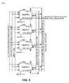
- FIG. 5is a detailed block diagram of the present invention.
- FIG. 6is a timing diagram illustrating an operation of the present invention.
- FIG. 3a block diagram of a system (or circuit) 100 is shown in accordance with a preferred embodiment of the present invention.
- the circuit 100may implement an out-of-band look-ahead arbitration method for transferring data bus control between multiple devices while in a queue expansion mode. Additionally, the circuit 100 may implement such control without a clock cycle penalty.
- the system 100generally comprises a read device 102 , a write device 103 and a memory section 104 .
- the memory section 104generally comprises a number of devices 106 a - 106 n .
- Each of the devices 106 a - 106 nmay be implemented as a multiqueue FIFO device.
- a boundary 108shows an interface between a portion of the devices 106 a - 106 n that operate at a first clock (e.g., a system clock) and a second portion that operates at a second clock (e.g., an interface clock).
- each of the multiqueue FIFO devices 106 a - 106 nmay comprise a clock synchronization block (or circuit) 110 that may synchronize the two clock domains.
- the read device 102may present a signal (e.g., RD_CONTROL) and a signal (e.g., RD_ADDR) to the memory section 104 .
- the read device 102may also present/receive a signal (e.g., RD_STATUS) to/from the memory section 104 .
- the read device 102may receive data (e.g., RD_DATA) from the memory section 104 .
- the write device 103may present a signal (e.g., WR_CONTROL) and a signal (e.g., WR_ADDR) to the memory section 104 .
- the write device 103may also present/receive a signal (e.g., WR_STATUS) to/from the memory section 104 . Additionally, the write device 103 may present data (e.g., WR_DATA) to the memory section 104 .
- a signale.g., WR_STATUS
- datae.g., WR_DATA
- Each of the various signals of the system 100may be implemented as a multi-bit and/or single-bit signal in order to meet the criteria of a particular implementation.
- the circuit 100may be implemented as a multiqueue FIFO with four master devices. Additionally, the circuit 100 may allow for queue expansion.
- the circuit 100may have a number of signals that have been modified, or are completely new when compared with the circuit 10 of FIG. 2 .
- the signal WHSHAKE, the signal RM[ 1 : 0 ], the signal Q_ADDR_REQ, the signal QNE and the signal CDhave been modified to be bidirectional signals. A number of new signals have been added to allow for queue expansion with four master devices.
- the signals WAQE[ 1 : 0 ], WMQE[ 1 : 0 ], DEVID[ 1 : 0 ], QEXP, EXP, RAQE[ 1 : 0 ], RMQE[ 1 : 0 ], ADDR_REQ, Q_EMPTY(@SYSCLK), QNE_SYNC, MINTB_SYNC, DTPA_SYNC, DTPA_SThave been added.
- any number of signalsmay be modified and/or added to meet the criteria of a particular implementation.
- each of the various signals of the circuit 100may be implemented as single-bit and/or multi-bit signals in a parallel or serial configuration.
- the signals having the notation “@SYSCLK”are generally clocked by the system clock.
- FIG. 4may illustrate additional pins for cascading four of the devices 106 a - 106 n
- the circuit 100is not limited to the four devices 106 a - 106 n .
- a fewer number or a greater number of the devices 106 a - 106 nmay be implemented accordingly to meet the design criteria of a particular implementation.
- An appropriate number and/or configuration of interface pinsmay be implemented, respectively.
- FIG. 5may illustrate queue expansion by cascading a number of the multiqueue devices 106 a - 106 n .
- the present inventionrelates to expansion of queues for multiqueue devices by cascading the devices 106 a - 106 n .
- the circuit 100may define an architecture to implement such multiqueue expansion.
- the circuit 100may provide an architecture for realizing N times the number of attached queues by cascading N such devices, where N is an integer.
- Each device 106 a - 106 nis generally assigned a unique identification value (e.g., DEVID), and is programmed for master configuration. For example, when cascading 4 devices, 2 bits of the signal DEVID may be required. For N bits of the signal DEVID, queue expansion for up to 2 N devices may be implemented.
- Each of the devices 106 a - 106 nmay only validate an access when the corresponding expanded address space is the same as the signal DEVID of the particular multiqueue FIFO 106 a - 106 n.
- each device 106 a - 106 nmay be connected to an active state to indicate that the circuit 100 is in the queue expansion mode.
- Each of the multiqueue FIFOs 106 a - 106 nmay also require a number of addresses.
- each of the multiqueue FIFOs 106 a - 106 nmay receive the signals write queue address (e.g., WAQE), write management register address (e.g., WMQE), read queue address (e.g., RAQE) and read management register address (e.g., RMQE).
- Each of the signals WAQE, WMQE, RAQE and RMQEmay be implemented as queue expansion signals.
- Each of the queue expansion signals WAQE, WMQE and RMQEmay have a number of queue expansion bits.
- the queue expansion bitsmay be compared with a particular device ID (e.g., DEVID) of each of the devices 106 a - 106 n .
- the queue expansion bitsmay be implemented to select an appropriate device 106 a - 106 n .
- the queue expansion signals WAQE, WMQE, RAQE and RMQEmay be only required during a queue expansion mode of operation.
- Each of the multiqueue FIFOs 106 a - 106 nmay interface with the bidirectional signals RM[ 1 : 0 ], EOP, Q_EMPTY, and EXP. Each of the addresses may be expanded by a same number of bits as the signal DEVID. Standard inputs and outputs of the circuit 100 may be wired together, as if the cascaded devices 106 a - 106 n represent one single device to external devices.
- the data outputs of the multiqueue FIFOs 106 a - 106 nmay be implemented as tristate outputs to allow the presentation of data from one device at a time.
- the circuit 100may provide self-arbitration of required output drivers (not shown). The circuit 100 may also allow for variable packet size handling capacity.
- the circuit 100may implement a wait cycle between driving of a particular bus by two of the devices 106 a - 106 n . However, such a wait state is generally optional. Additional implementations of the circuit 100 may include back-to-back reads, or a gap cycle between two sequential reads.
- Existing control output signalsmay be implemented as typical I/Os with the exception of the signal MS/CQS.
- the other devicese.g., 106 b - 106 n
- Such an implementationmay allow the multiqueue FIFOs 106 a - 106 n to operate synchronously.
- the devices 106 a - 106 nare generally synchronized by various signals.
- the signal EXPis outputted by one multiqueue device (e.g., 106 a ) to the remaining multiqueue devices (e.g., 106 b - 106 n ).
- the device 106 agenerally communicates which clock (read clock or write clock) is chosen as the system clock. Details of which can be found in the related cross reference applications.
- the signal ADDR_REQ (@SYSCLK), together with the signal RM (which indicates an end of packet EOP) and the signals Q_EMPTYallow the read queue address to be processed sequentially by all the devices 106 a - 106 n.
- the timing diagram 200may illustrate status polling for queue expansion of a number of devices.
- a signale.g., RCLK
- a signale.g., QNE
- the effective status of the system 100e.g., the device 106 a - 106 n .
- the signal QNEmay be implemented as a queue not enable signal configured to indicate an enabled/not enabled state of the system 100 .
- the signal QNEmay indicate an effective status of all the devices (e.g., DEV 0 , DEV 1 , DEV 2 or DEV 3 ) of the timing diagram 200 .
- the signal QNEmay be implemented as a wired AND of a number of queue not enable signals (e.g., QNE_DEV 0 , QNE_DEV 1 , QNE_DEV 2 and/or QEN_DEV 3 ). Additionally, the signals QNE_DEV 0 , QNE_DEV 1 , QNE_DEV 2 and QNE_DEV 3 may illustrate status polling of the various devices 106 a - 106 n .
- a signal(e.g., QNE_SYNC) may indicate which device (e.g., a particular one of the devices DEV 0 , DEV 1 , DEV 2 or DEV 3 ) may present an output.
- the present inventionmay allow two methods of communicating status information for each multiqueue FIFO 106 a - 106 n .
- the status informationmay also be communicated in a synchronous manner.
- One methodmay require three pins where all of the interface signals may be implemented as point-to-point signals.
- Another methodmay require a single pin where the interface signal may be implemented as point-to-multipoint signal.
- the status signals(e.g., the signal QNE and the signal MINTB) may be polled in a burst manner with the help of the control signals QNE_SYNC and MINTB_SYNC, respectively. Such status polling is shown in FIG. 4 and FIG. 6, for expansion up to four multiqueue devices.
- the signal QNE_SYNCmay indicate when each device outputs the status with respect to the signal.
- the control signals QNE_SYNC and MINTB_SYNCmay allow an external device to compute the QNE and MINTB information for each multiqueue devices 106 a - 106 n .
- the data porte.g., packet-over-SONET physical layer (POS-PHY), supported by a status pin
- POS-PHYpacket-over-SONET physical layer
- the signal DTPA_SYNCoutputted by the multiqueue device 106 a , provides a point-to-point signal bearing the timing information for the signal DTPA.
- the circuit 100may implement two kinds of arbitration.
- the first arbitration methodmay allow the devices 106 a - 106 n to directly arbitrate based on the expansion address. For example, the data read out through the management interface will depend on the management register address expansion most significant bits (e.g., WMQE or RMQE). Similarly, arbitration of the signal WHSHAKE depends on the write queue address expansion most significant bits.
- the second arbitration methodmay involve early prediction, especially when an end at an access is not known. Such a method may require the devices 106 a - 106 n to act synchronously with respect to events.
- the read datais arbitrated using such a method.
- the read arbitrationallows for variable size packets to be passed through, and also allows a dual clock system.
- An EOP indicationvia the clock signal ADDR_REQ@SYSCLK
- the queue empty indicationvia the clock signal Q_EMPTY@SYSCLK
- the circuit 100may provide a multiqueue expansion architecture implementing device ID inputs (e.g., the signal DEVID) for deciding queue/register address MSB bits.
- the circuit 100may specifically implement write queue address expansion bits for writing into the expanded queues, write management register address expansion bits for accessing registers belonging to the other devices, read queue address expansion bits for reading from the expanded queues, and/or read management register address expansion bits for accessing registers belonging to the other devices.
- the circuit 100may further implement tristatable output data buses and output control buses for arbitration.
- the circuit 100may implement an interface for synchronous status polling across devices.
- the circuit 100may allow for a faster clock synchronization interface.
- the circuit 100may also allow for variable size packet handling capacity.
Landscapes
- Engineering & Computer Science (AREA)
- Theoretical Computer Science (AREA)
- General Engineering & Computer Science (AREA)
- Physics & Mathematics (AREA)
- General Physics & Mathematics (AREA)
- Computer Hardware Design (AREA)
- Communication Control (AREA)
Abstract
Description
Claims (22)
Priority Applications (1)
| Application Number | Priority Date | Filing Date | Title |
|---|---|---|---|
| US09/714,441US6625711B1 (en) | 2000-11-16 | 2000-11-16 | Method and/or architecture for implementing queue expansion in multiqueue devices |
Applications Claiming Priority (1)
| Application Number | Priority Date | Filing Date | Title |
|---|---|---|---|
| US09/714,441US6625711B1 (en) | 2000-11-16 | 2000-11-16 | Method and/or architecture for implementing queue expansion in multiqueue devices |
Publications (1)
| Publication Number | Publication Date |
|---|---|
| US6625711B1true US6625711B1 (en) | 2003-09-23 |
Family
ID=28042357
Family Applications (1)
| Application Number | Title | Priority Date | Filing Date |
|---|---|---|---|
| US09/714,441Expired - LifetimeUS6625711B1 (en) | 2000-11-16 | 2000-11-16 | Method and/or architecture for implementing queue expansion in multiqueue devices |
Country Status (1)
| Country | Link |
|---|---|
| US (1) | US6625711B1 (en) |
Cited By (5)
| Publication number | Priority date | Publication date | Assignee | Title |
|---|---|---|---|---|
| US6816979B1 (en) | 2001-02-01 | 2004-11-09 | Cypress Semiconductor Corp. | Configurable fast clock detection logic with programmable resolution |
| US7047312B1 (en)* | 2000-07-26 | 2006-05-16 | Nortel Networks Limited | TCP rate control with adaptive thresholds |
| US7225283B1 (en) | 2003-12-23 | 2007-05-29 | Cypress Semiconductor Corporation | Asynchronous arbiter with bounded resolution time and predictable output state |
| US7343510B1 (en) | 2003-12-22 | 2008-03-11 | Cypress Semiconductor Corporation | Method and device for selecting one of multiple clock signals based on frequency differences of such clock signals |
| US7383370B1 (en) | 2005-03-31 | 2008-06-03 | Cypress Semiconductor Corporation | Arbiter circuit and signal arbitration method |
Citations (12)
| Publication number | Priority date | Publication date | Assignee | Title |
|---|---|---|---|---|
| US5121485A (en)* | 1988-05-28 | 1992-06-09 | Nec Corporation | Multi-system bus connected via interface side buffering interstage buffers, and cpu side buffers to cpu i/o bus and slave system |
| US5185879A (en)* | 1988-01-21 | 1993-02-09 | Akira Yamada | Cache system and control method therefor |
| US5640515A (en)* | 1993-10-28 | 1997-06-17 | Daewoo Electronics Co., Ltd. | FIFO buffer system having enhanced controllability |
| US5812875A (en)* | 1995-05-02 | 1998-09-22 | Apple Computer, Inc. | Apparatus using a state device and a latching circuit to generate an acknowledgement signal in close proximity to the request signal for enhancing input/output controller operations |
| US5859718A (en)* | 1994-12-28 | 1999-01-12 | Canon Kabushiki Kaisha | Simplified switching control device, and a network system for employing the device: and a simplified switching control method, and a communication method for employing the method |
| US5870572A (en)* | 1991-07-22 | 1999-02-09 | International Business Machines Corporation | Universal buffered interface for coupling multiple processors, memory units, and I/O interfaces to a common high-speed interconnect |
| US5872787A (en)* | 1996-05-15 | 1999-02-16 | Gte Laboratories Incorporated | Distributed switch buffer utilizing cascaded modular switch chips |
| US6215769B1 (en)* | 1998-10-07 | 2001-04-10 | Nokia Telecommunications, Inc. | Enhanced acknowledgment pacing device and method for TCP connections |
| US6292877B1 (en)* | 1997-07-01 | 2001-09-18 | Micron Technology, Inc. | Plural pipelined packet-oriented memory systems having a unidirectional command and address bus and a bidirectional data bus |
| US6295295B1 (en)* | 1995-11-27 | 2001-09-25 | Telefonaktiebolaget Lm Ericsson | Scheduler for an information packet switch |
| US6339596B1 (en)* | 1987-07-15 | 2002-01-15 | Hitachi, Ltd. | ATM cell switching system |
| US6526495B1 (en)* | 2000-03-22 | 2003-02-25 | Cypress Semiconductor Corp. | Multiport FIFO with programmable width and depth |
- 2000
- 2000-11-16USUS09/714,441patent/US6625711B1/ennot_activeExpired - Lifetime
Patent Citations (12)
| Publication number | Priority date | Publication date | Assignee | Title |
|---|---|---|---|---|
| US6339596B1 (en)* | 1987-07-15 | 2002-01-15 | Hitachi, Ltd. | ATM cell switching system |
| US5185879A (en)* | 1988-01-21 | 1993-02-09 | Akira Yamada | Cache system and control method therefor |
| US5121485A (en)* | 1988-05-28 | 1992-06-09 | Nec Corporation | Multi-system bus connected via interface side buffering interstage buffers, and cpu side buffers to cpu i/o bus and slave system |
| US5870572A (en)* | 1991-07-22 | 1999-02-09 | International Business Machines Corporation | Universal buffered interface for coupling multiple processors, memory units, and I/O interfaces to a common high-speed interconnect |
| US5640515A (en)* | 1993-10-28 | 1997-06-17 | Daewoo Electronics Co., Ltd. | FIFO buffer system having enhanced controllability |
| US5859718A (en)* | 1994-12-28 | 1999-01-12 | Canon Kabushiki Kaisha | Simplified switching control device, and a network system for employing the device: and a simplified switching control method, and a communication method for employing the method |
| US5812875A (en)* | 1995-05-02 | 1998-09-22 | Apple Computer, Inc. | Apparatus using a state device and a latching circuit to generate an acknowledgement signal in close proximity to the request signal for enhancing input/output controller operations |
| US6295295B1 (en)* | 1995-11-27 | 2001-09-25 | Telefonaktiebolaget Lm Ericsson | Scheduler for an information packet switch |
| US5872787A (en)* | 1996-05-15 | 1999-02-16 | Gte Laboratories Incorporated | Distributed switch buffer utilizing cascaded modular switch chips |
| US6292877B1 (en)* | 1997-07-01 | 2001-09-18 | Micron Technology, Inc. | Plural pipelined packet-oriented memory systems having a unidirectional command and address bus and a bidirectional data bus |
| US6215769B1 (en)* | 1998-10-07 | 2001-04-10 | Nokia Telecommunications, Inc. | Enhanced acknowledgment pacing device and method for TCP connections |
| US6526495B1 (en)* | 2000-03-22 | 2003-02-25 | Cypress Semiconductor Corp. | Multiport FIFO with programmable width and depth |
Non-Patent Citations (6)
| Title |
|---|
| S. Babar Raza et al., "Architecture For Implementing Virtual Multiqueue Fifos", U.S. Ser. No. 09/676,704, Filed Sep. 29, 2000. |
| S. Babar Raza et al., "Logic for Generating Multicast/Unicast Address(es)", U.S. Ser. No. 09/676,706, Filed Sep. 29, 2000. |
| S. Babar Raza et al., "Logic for Initializing the Depth of the Queue Pointer Memory", U.S. Ser. No. 09/676,705, Filed Sep. 29, 2000. |
| S. Babar Raza et al., "Logic for Providing Arbitration for Synchronous Dual-Port Memory", U.S. Ser. No. 09/676,169, Filed Sep. 29, 2000. |
| S. Babar Raza et al., "Method and Logic for Initializing the Forward-Pointer Memory During Normal Operation of the Device as a Background Process", U.S. Ser. No. 09/676,170, Filed Sep. 29, 2000. |
| S. Babar Raza et al., "Method and Logic For Storing and Extracting In-Band Multicast Port Information Stored Along with the Data in a Single Memory Without Memory Read Cycle Overhead", U.S. Ser. No. 09/676,171, Filed Sep. 29, 2000. |
Cited By (5)
| Publication number | Priority date | Publication date | Assignee | Title |
|---|---|---|---|---|
| US7047312B1 (en)* | 2000-07-26 | 2006-05-16 | Nortel Networks Limited | TCP rate control with adaptive thresholds |
| US6816979B1 (en) | 2001-02-01 | 2004-11-09 | Cypress Semiconductor Corp. | Configurable fast clock detection logic with programmable resolution |
| US7343510B1 (en) | 2003-12-22 | 2008-03-11 | Cypress Semiconductor Corporation | Method and device for selecting one of multiple clock signals based on frequency differences of such clock signals |
| US7225283B1 (en) | 2003-12-23 | 2007-05-29 | Cypress Semiconductor Corporation | Asynchronous arbiter with bounded resolution time and predictable output state |
| US7383370B1 (en) | 2005-03-31 | 2008-06-03 | Cypress Semiconductor Corporation | Arbiter circuit and signal arbitration method |
Similar Documents
| Publication | Publication Date | Title |
|---|---|---|
| EP2350847B1 (en) | Method and system for improving serial port memory communication latency and reliability | |
| US6044416A (en) | Configurable first-in first-out memory interface | |
| US6920510B2 (en) | Time sharing a single port memory among a plurality of ports | |
| US6816955B1 (en) | Logic for providing arbitration for synchronous dual-port memory | |
| US20020184453A1 (en) | Data bus system including posted reads and writes | |
| JPH05204825A (en) | Direct memory-access-controller and information processor | |
| KR20040106303A (en) | Memory system with burst length shorter than prefetch length | |
| CN1885430A (en) | Parallel Datapath Architecture | |
| US20120117286A1 (en) | Interface Devices And Systems Including The Same | |
| US7016349B1 (en) | Logic for generating multicast/unicast address (es) | |
| JPH04350754A (en) | Workstation including interface for data channel or similar data processing system | |
| US6625711B1 (en) | Method and/or architecture for implementing queue expansion in multiqueue devices | |
| US6631455B1 (en) | Logic for initializing the depth of the queue pointer memory | |
| US7136309B2 (en) | FIFO with multiple data inputs and method thereof | |
| US6925506B1 (en) | Architecture for implementing virtual multiqueue fifos | |
| US7870310B2 (en) | Multiple counters to relieve flag restriction in a multi-queue first-in first-out memory system | |
| US6578118B1 (en) | Method and logic for storing and extracting in-band multicast port information stored along with the data in a single memory without memory read cycle overhead | |
| US6487140B2 (en) | Circuit for managing the transfer of data streams from a plurality of sources within a system | |
| JPH07191901A (en) | Holding device of data information | |
| US6715021B1 (en) | Out-of-band look-ahead arbitration method and/or architecture | |
| US6483753B1 (en) | Endianess independent memory interface | |
| EP0382342B1 (en) | Computer system DMA transfer | |
| US6581144B1 (en) | Method and logic for initializing the forward-pointer memory during normal operation of the device as a background process | |
| JP4904136B2 (en) | Single-port memory controller for bidirectional data communication and control method thereof | |
| JP3028932B2 (en) | Input/Output Buffer Memory Circuit |
Legal Events
| Date | Code | Title | Description |
|---|---|---|---|
| AS | Assignment | Owner name:CYPRESS SEMICONDUCTOR CORPORATION, CALIFORNIA Free format text:ASSIGNMENT OF ASSIGNORS INTEREST;ASSIGNORS:RAZA, S. BABER;PAUL, SOMNATH;REEL/FRAME:011312/0781 Effective date:20001115 | |
| STCF | Information on status: patent grant | Free format text:PATENTED CASE | |
| FPAY | Fee payment | Year of fee payment:4 | |
| FPAY | Fee payment | Year of fee payment:8 | |
| FPAY | Fee payment | Year of fee payment:12 | |
| AS | Assignment | Owner name:MORGAN STANLEY SENIOR FUNDING, INC., NEW YORK Free format text:SECURITY INTEREST;ASSIGNORS:CYPRESS SEMICONDUCTOR CORPORATION;SPANSION LLC;REEL/FRAME:035240/0429 Effective date:20150312 | |
| AS | Assignment | Owner name:SPANSION LLC, CALIFORNIA Free format text:PARTIAL RELEASE OF SECURITY INTEREST IN PATENTS;ASSIGNOR:MORGAN STANLEY SENIOR FUNDING, INC., AS COLLATERAL AGENT;REEL/FRAME:039708/0001 Effective date:20160811 Owner name:CYPRESS SEMICONDUCTOR CORPORATION, CALIFORNIA Free format text:PARTIAL RELEASE OF SECURITY INTEREST IN PATENTS;ASSIGNOR:MORGAN STANLEY SENIOR FUNDING, INC., AS COLLATERAL AGENT;REEL/FRAME:039708/0001 Effective date:20160811 | |
| AS | Assignment | Owner name:MONTEREY RESEARCH, LLC, CALIFORNIA Free format text:ASSIGNMENT OF ASSIGNORS INTEREST;ASSIGNOR:CYPRESS SEMICONDUCTOR CORPORATION;REEL/FRAME:040911/0238 Effective date:20160811 | |
| AS | Assignment | Owner name:MORGAN STANLEY SENIOR FUNDING, INC., NEW YORK Free format text:CORRECTIVE ASSIGNMENT TO CORRECT THE 8647899 PREVIOUSLY RECORDED ON REEL 035240 FRAME 0429. ASSIGNOR(S) HEREBY CONFIRMS THE SECURITY INTERST;ASSIGNORS:CYPRESS SEMICONDUCTOR CORPORATION;SPANSION LLC;REEL/FRAME:058002/0470 Effective date:20150312 |