US6625706B2 - ATD generation in a synchronous memory - Google Patents
ATD generation in a synchronous memoryDownload PDFInfo
- Publication number
- US6625706B2 US6625706B2US09/773,760US77376001AUS6625706B2US 6625706 B2US6625706 B2US 6625706B2US 77376001 AUS77376001 AUS 77376001AUS 6625706 B2US6625706 B2US 6625706B2
- Authority
- US
- United States
- Prior art keywords
- pulse
- atd
- array
- atd pulse
- dummy
- Prior art date
- Legal status (The legal status is an assumption and is not a legal conclusion. Google has not performed a legal analysis and makes no representation as to the accuracy of the status listed.)
- Expired - Lifetime, expires
Links
- 230000015654memoryEffects0.000titleclaimsabstractdescription67
- 230000001360synchronised effectEffects0.000titleclaimsabstractdescription20
- 238000000034methodMethods0.000claimsabstractdescription21
- 239000000872bufferSubstances0.000claimsdescription18
- 230000006870functionEffects0.000claimsdescription11
- 238000001514detection methodMethods0.000abstractdescription3
- 238000010586diagramMethods0.000description8
- 238000013459approachMethods0.000description5
- 239000011159matrix materialSubstances0.000description5
- 230000008901benefitEffects0.000description3
- 230000008859changeEffects0.000description2
- 230000000087stabilizing effectEffects0.000description2
- XUIMIQQOPSSXEZ-UHFFFAOYSA-NSiliconChemical compound[Si]XUIMIQQOPSSXEZ-UHFFFAOYSA-N0.000description1
- 230000001934delayEffects0.000description1
- 230000001419dependent effectEffects0.000description1
- 238000005265energy consumptionMethods0.000description1
- 238000011156evaluationMethods0.000description1
- 238000000605extractionMethods0.000description1
- 230000007246mechanismEffects0.000description1
- 230000008569processEffects0.000description1
- 238000012545processingMethods0.000description1
- 230000000630rising effectEffects0.000description1
- 229910052710siliconInorganic materials0.000description1
- 239000010703siliconSubstances0.000description1
- 230000000638stimulationEffects0.000description1
- 230000001629suppressionEffects0.000description1
- 238000012546transferMethods0.000description1
- 230000007704transitionEffects0.000description1
- 230000001960triggered effectEffects0.000description1
Images


Classifications
- G—PHYSICS
- G11—INFORMATION STORAGE
- G11C—STATIC STORES
- G11C7/00—Arrangements for writing information into, or reading information out from, a digital store
- G11C7/10—Input/output [I/O] data interface arrangements, e.g. I/O data control circuits, I/O data buffers
- G11C7/1051—Data output circuits, e.g. read-out amplifiers, data output buffers, data output registers, data output level conversion circuits
- G11C7/1057—Data output buffers, e.g. comprising level conversion circuits, circuits for adapting load
- G—PHYSICS
- G11—INFORMATION STORAGE
- G11C—STATIC STORES
- G11C7/00—Arrangements for writing information into, or reading information out from, a digital store
- G11C7/10—Input/output [I/O] data interface arrangements, e.g. I/O data control circuits, I/O data buffers
- G11C7/1015—Read-write modes for single port memories, i.e. having either a random port or a serial port
- G11C7/1018—Serial bit line access mode, e.g. using bit line address shift registers, bit line address counters, bit line burst counters
- G—PHYSICS
- G11—INFORMATION STORAGE
- G11C—STATIC STORES
- G11C7/00—Arrangements for writing information into, or reading information out from, a digital store
- G11C7/10—Input/output [I/O] data interface arrangements, e.g. I/O data control circuits, I/O data buffers
- G11C7/1015—Read-write modes for single port memories, i.e. having either a random port or a serial port
- G11C7/1039—Read-write modes for single port memories, i.e. having either a random port or a serial port using pipelining techniques, i.e. using latches between functional memory parts, e.g. row/column decoders, I/O buffers, sense amplifiers
- G—PHYSICS
- G11—INFORMATION STORAGE
- G11C—STATIC STORES
- G11C7/00—Arrangements for writing information into, or reading information out from, a digital store
- G11C7/10—Input/output [I/O] data interface arrangements, e.g. I/O data control circuits, I/O data buffers
- G11C7/1015—Read-write modes for single port memories, i.e. having either a random port or a serial port
- G11C7/1042—Read-write modes for single port memories, i.e. having either a random port or a serial port using interleaving techniques, i.e. read-write of one part of the memory while preparing another part
- G—PHYSICS
- G11—INFORMATION STORAGE
- G11C—STATIC STORES
- G11C7/00—Arrangements for writing information into, or reading information out from, a digital store
- G11C7/10—Input/output [I/O] data interface arrangements, e.g. I/O data control circuits, I/O data buffers
- G11C7/1015—Read-write modes for single port memories, i.e. having either a random port or a serial port
- G11C7/1045—Read-write mode select circuits
- G—PHYSICS
- G11—INFORMATION STORAGE
- G11C—STATIC STORES
- G11C7/00—Arrangements for writing information into, or reading information out from, a digital store
- G11C7/10—Input/output [I/O] data interface arrangements, e.g. I/O data control circuits, I/O data buffers
- G11C7/1051—Data output circuits, e.g. read-out amplifiers, data output buffers, data output registers, data output level conversion circuits
- G11C7/106—Data output latches
- G—PHYSICS
- G11—INFORMATION STORAGE
- G11C—STATIC STORES
- G11C7/00—Arrangements for writing information into, or reading information out from, a digital store
- G11C7/10—Input/output [I/O] data interface arrangements, e.g. I/O data control circuits, I/O data buffers
- G11C7/1051—Data output circuits, e.g. read-out amplifiers, data output buffers, data output registers, data output level conversion circuits
- G11C7/1069—I/O lines read out arrangements
- G—PHYSICS
- G11—INFORMATION STORAGE
- G11C—STATIC STORES
- G11C7/00—Arrangements for writing information into, or reading information out from, a digital store
- G11C7/10—Input/output [I/O] data interface arrangements, e.g. I/O data control circuits, I/O data buffers
- G11C7/1072—Input/output [I/O] data interface arrangements, e.g. I/O data control circuits, I/O data buffers for memories with random access ports synchronised on clock signal pulse trains, e.g. synchronous memories, self timed memories
- G—PHYSICS
- G11—INFORMATION STORAGE
- G11C—STATIC STORES
- G11C7/00—Arrangements for writing information into, or reading information out from, a digital store
- G11C7/22—Read-write [R-W] timing or clocking circuits; Read-write [R-W] control signal generators or management
- G—PHYSICS
- G11—INFORMATION STORAGE
- G11C—STATIC STORES
- G11C8/00—Arrangements for selecting an address in a digital store
- G11C8/04—Arrangements for selecting an address in a digital store using a sequential addressing device, e.g. shift register, counter
- G—PHYSICS
- G11—INFORMATION STORAGE
- G11C—STATIC STORES
- G11C8/00—Arrangements for selecting an address in a digital store
- G11C8/18—Address timing or clocking circuits; Address control signal generation or management, e.g. for row address strobe [RAS] or column address strobe [CAS] signals
Definitions
- the present inventionrelates in general to memory devices, and in particular, to an interleaved memory readable in a synchronous mode or in a random access asynchronous mode with fast access times.
- the interleaved memoryis readable in the synchronous mode by successive locations with a sequential type of access, commonly referred to as a burst mode.
- a read cyclespans from a request of data by way of the switching of the input address lines to the final extraction of the bits stored in the addressed memory location.
- the read circuitryreferences, sense amplifiers, etc.
- the start of a new readingmust be triggered by the generation of a suitable signal (Address Transition Detection pulse or briefly ATD) that is generally produced by a circuit sensing a change of the input address.
- a typical ATD pulse generatoris depicted in FIG. 1 .
- the ATD pulsemust satisfy fundamental requirements for a correct reading and for satisfying the access time requirements.
- the ATDmust be generated as quick as possible in order to quickly restart the whole analog sensing networks.
- a common ATD pulse generatoris unsuitable because the external address lines do not switch (or are not accessible to the memory device) during synchronous read cycles.
- a different approachcould be that of placing the ATD generation circuit in cascade of the counter that generates the internal addresses, instead of in cascade of the input address buffer. This is done to always generate the pulses at the same point of the control chain, independently of the kind of access in progress. During the asynchronous reading the counter works as a register because the internal and external addresses coincide.
- the present inventionprovides an approach using an ATD signal even for starting sequential readings, by causing its generation when the start of a new cycle of synchronous readings with sequential access is detected.
- the most appropriate signal to provide such informationis the increment pulse for the internal address counter.
- this increment pulseit is possible to generate a pseudo ATD signal, i.e., stimulated by an internal cause and not by the switching of the external address lines. This starts a new reading.
- the final architecturemaintains the classical structure of ATD generation, with circuits sensing the external address lines (useful for all conventional accesses) and sensing the pulses of sequential increment of an internal address counter, and generating the ATD pulses for starting sequential readings.
- the method of the invention for synchronizing the start of sequential readings for a read cycle of a memory in burst synchronous modeincludes using the increment pulses of the address counter, or of the address counters in the case of interleaved memory devices, as synchronization signals, by generating after each increment pulse a dummy ATD pulse.
- the dummy ATD pulseis practically undistinguishable from an ATD pulse generated by an effective switching of the input address latches.
- an ATD pulse generatorconventionally sensing the external address lines is used, but modified to include at least a pulse generator circuit stimulated by an increment pulse synchronized by a respective address counter.
- the method of the inventioncan advantageously contemplate the fact that the increment pulses are distinct for the counter of one of the banks of the array of cells of the interleaved memory.
- the distinct increment pulses producedcorresponds to distinct dummy ATD pulses for starting sequential readings in the respective subdivided banks of the array of cells of the interleaved memory.
- An external protocol signal(ALE), or more generally, an equivalent command ENABLE for enabling the input latch or latches of acquisition of external input addresses determines, as a function of its logic state, the generation of ATD pulses common to both the subdivided banks of the matrix (array) of cells of the interleaved memory. This is done for read cycles in a random access asynchronous mode or, according to the invention, the generation of dummy ATD pulses specifically for one of the subdivided banks of the matrix of cells of the interleaved memory for a synchronous read cycle in burst access.
- ALEexternal protocol signal
- the ALE signalestablishes that it is necessary to start a read cycle from an external address. For such a cycle, either the first random cycle of a sequence of burst readings or a generic asynchronous access, the ATD pulse stimulated by the switching of the external address lines is sent to all the banks, which will then enable their respective read structures.
- Bank priorityis defined by the least significant bit A ⁇ 0> of the address, as already explained.
- the control logic of the memorywill generate a first increment pulse for the address counter of the bank (or banks) that is not in priority, such as the bank ODD, for example. This is done to generate the address on which the following (second) reading will be carried out.
- a new dummy ATD pulseis generated to start a new read cycle on the ODD bank, i.e., on the bank whose internal address is being incremented. In this way, the reading on the bank EVEN is left to evolve.
- a new dummy ATD pulsefollowing the generation of an internal address counter increment pulse, the reading on the other bank ODD is restarted with the updated internal address.
- a new increment pulse INC_Ewill be generated. This pulse is intended for the address counter of the EVEN bank on which the reading has just terminated.
- a new ATD pulse dedicated to the bank EVENwill be generated to restart a new reading, while the ODD bank, having acquired priority from the control logic, will be completing the reading cycle as far as to output of the read data.
- dedicated ATD pulsesare coordinately generated to start the readings on the two banks in an alternate fashion.
- FIG. 1shows a classical structure for generating ATD pulses from the switching of external addresses according to the prior art
- FIG. 2is a basic diagram of the architecture for generating ATD pulses for synchronous memories according to the present invention
- FIG. 3illustrates graphically the ATD pulse generation processes in the case of a random access and in the case of sequential access (burst) according to the prior art
- FIG. 4shows a simplified block diagram of an interleaved memory according to the prior art
- FIG. 5illustrates graphically the dependence between the increment pulses and the generation of internal addresses for the two banks of an interleaved memory according to the prior art
- FIG. 6shows the time evolution of the main signal involved in the ATD pulse generation according to the prior art.
- FIG. 7is a diagram of the architecture according to an alternative embodiment that is particularly effective for interleaved memory devices according to the present invention.
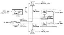
- FIG. 2The basic diagram of the architecture of the invention for a synchronous memory is depicted in FIG. 2 .
- the increment pulse of the address counteris identified as INC_COUNTER.
- the block CONTROL LOGICrepresents the logic circuit that generates the increment pulse INC_COUNTER, immediately after the detection of a rising edge of a synchronization signal of the synchronous readings, indicated as EXT_CLOCK in the diagram.
- FIG. 3The functioning of the circuit of the invention of FIG. 2 is diagrammatically depicted in FIG. 3 in the case of a random access (RAND ACCESS) and in the case of a sequential read cycle (SYNC ACCESS).
- RAND ACCESSrandom access
- SYNC ACCESSsequential read cycle
- the generation of the ATD pulsestakes place during the same logic phase of a reading, that is, when the latches that form the internal address counter are stabilizing themselves. This is whether the address is input from outside or it is internally generated through an incrementing of the counter itself. In this way, the same propagation delay of the ATD pulses that would be experienced during a standard random access read cycle is ensured also in case of sequential synchronous reading cycles.
- FIG. 4A simplified block diagram of a typical two-bank interleaved memory is depicted in FIG. 4 .
- the matrixis divided into two independent banks, EVEN MATRIX and ODD MATRIX, each one having its own read path structure.
- the read cycles of the two banksmay then superimpose to one another even though they are out of phase.
- evaluation and transfer of the data to the outputis being carried out (OUTPUT BUFFER)
- on the other bankby virtue of the fact that the location to be addressed is known it is possible to start a new reading without waiting for the conclusion of the reading in progress on the first one.
- CONTROLtied to the external synchronization clock
- CONTROLBy way of a control signal, CONTROL, tied to the external synchronization clock, it is possible to manage the multiplexing with respect to the output MUX, alternating the priority from one bank to the other. Therefore, for readings successive to the first one, in order to exploit the contiguity of addresses it is necessary to generate addresses internally by the respective counters, EVEN COUNTER and ODD COUNTER. These counters are incremented coherently with the system's clock by the respective increment pulses INC_EVEN and INC_ODD.
- FIG. 5The dependence among the specific increment pulses and the generation (sequential updating) of the internal addresses of the two banks is graphically depicted in FIG. 5 .
- FIG. 6An example of the timing of the main involved signals is depicted in FIG. 6 .
- the basic diagram of FIG. 2can be modified as depicted in FIG. 7 . It still comprises the classic ATD pulse generation structure based on circuits sensing switching of the external address lines. The ATD pulses generated by these circuits sensing the external address lines are common for the two banks and are used for all conventional random accesses.
- Substantially the structure of the ATD pulse generator of FIG. 7comprises, instead of a single auxiliary pulse generator, two auxiliary pulse generators, EVEN PULSER and ODD PULSER. These pulse generators are stimulated by specific increment signals INC_EVEN COUNTER and INC_ODD COUNTER, respectively, for the internal address counter of the EVEN bank and for the internal address counter of the ODD band which generate specific dummy ATD pulses: EVEN_ATD and ODD_ATD for the two banks for interleaved sequential readings.
- INC_EVEN COUNTERand INC_ODD COUNTER
- the path of the control signalsstarts from the ATD pulse in case of sequential access reading is the same of that in case of a random access reading.
- the generation of ATD pulsestakes place in the same logic phase of a reading, i.e., when the latches that form the internal address counter are stabilizing themselves. This is whether the address is input from outside or it is internally generated through an incrementing of one of the counters.
- An additional advantageis represented by the exploitation of the distinct increment pulses for the internal address counters of the two banks. In this way, no further processing is necessary for correctly conveying the dummy ATD pulse to one bank without affecting the other bank.
- the alternative of generating a common ATD pulse and successively permitting propagation only toward the correct bankwould require, in practice, a further control signal for implementing the required multiplexing, e.g., a priority flag signal.
Landscapes
- Engineering & Computer Science (AREA)
- Microelectronics & Electronic Packaging (AREA)
- Dram (AREA)
Abstract
Description
Claims (26)
Applications Claiming Priority (5)
| Application Number | Priority Date | Filing Date | Title |
|---|---|---|---|
| EP00830068 | 2000-01-31 | ||
| EP00830068.3 | 2000-01-31 | ||
| EP00830068AEP1122734B1 (en) | 2000-01-31 | 2000-01-31 | Burst interleaved memory with burst mode access in synchronous read phases wherein the two sub-arrays are independently readable with random access during asynchronous read phases |
| EP00830313AEP1122736B1 (en) | 2000-01-31 | 2000-04-27 | ATD generation in a synchronous memory |
| EP00830313 | 2000-04-27 |
Publications (2)
| Publication Number | Publication Date |
|---|---|
| US20010029563A1 US20010029563A1 (en) | 2001-10-11 |
| US6625706B2true US6625706B2 (en) | 2003-09-23 |
Family
ID=26074118
Family Applications (1)
| Application Number | Title | Priority Date | Filing Date |
|---|---|---|---|
| US09/773,760Expired - LifetimeUS6625706B2 (en) | 2000-01-31 | 2001-01-31 | ATD generation in a synchronous memory |
Country Status (2)
| Country | Link |
|---|---|
| US (1) | US6625706B2 (en) |
| EP (1) | EP1122736B1 (en) |
Cited By (2)
| Publication number | Priority date | Publication date | Assignee | Title |
|---|---|---|---|---|
| US20040032779A1 (en)* | 2002-07-08 | 2004-02-19 | Nec Electronics Corporation | Semiconductor memory device |
| US9036446B2 (en) | 2012-02-27 | 2015-05-19 | Qualcomm Incorporated | Global reset with replica for pulse latch pre-decoders |
Families Citing this family (1)
| Publication number | Priority date | Publication date | Assignee | Title |
|---|---|---|---|---|
| DE60329316D1 (en) | 2002-11-12 | 2009-10-29 | Merck & Co Inc | PHENYL ACARBOXAMIDE AS A BETA SEKRETASE INHIBITOR FOR THE TREATMENT OF ALZHEIMER |
Citations (11)
| Publication number | Priority date | Publication date | Assignee | Title |
|---|---|---|---|---|
| EP0561370A2 (en) | 1992-03-19 | 1993-09-22 | Kabushiki Kaisha Toshiba | A clock-synchronous semiconductor memory device and access method thereof |
| US5559990A (en) | 1992-02-14 | 1996-09-24 | Advanced Micro Devices, Inc. | Memories with burst mode access |
| US5596539A (en) | 1995-12-28 | 1997-01-21 | Lsi Logic Corporation | Method and apparatus for a low power self-timed memory control system |
| US5657269A (en)* | 1994-08-09 | 1997-08-12 | Yamaha Corporation | Semiconductor storage device having address-transition detecting circuit and sense-determination detecting circuit |
| US5696917A (en)* | 1994-06-03 | 1997-12-09 | Intel Corporation | Method and apparatus for performing burst read operations in an asynchronous nonvolatile memory |
| US5859623A (en)* | 1996-05-14 | 1999-01-12 | Proxima Corporation | Intelligent display system presentation projection arrangement and method of using same |
| US5912860A (en)* | 1995-09-01 | 1999-06-15 | Micron Technology, Inc. | Synchronous DRAM memory with asynchronous column decode |
| US5963504A (en)* | 1994-12-23 | 1999-10-05 | Micron Technology, Inc. | Address transition detection in a synchronous design |
| US5966724A (en) | 1996-01-11 | 1999-10-12 | Micron Technology, Inc. | Synchronous memory device with dual page and burst mode operations |
| EP0961283A2 (en) | 1998-05-28 | 1999-12-01 | Fujitsu Limited | Memory circuit |
| US6470431B2 (en)* | 2000-01-31 | 2002-10-22 | Stmicroelectronics S.R.L. | Interleaved data path and output management architecture for an interleaved memory and load pulser circuit for outputting the read data |
Family Cites Families (1)
| Publication number | Priority date | Publication date | Assignee | Title |
|---|---|---|---|---|
| US5488587A (en)* | 1993-10-20 | 1996-01-30 | Sharp Kabushiki Kaisha | Non-volatile dynamic random access memory |
- 2000
- 2000-04-27EPEP00830313Apatent/EP1122736B1/ennot_activeExpired - Lifetime
- 2001
- 2001-01-31USUS09/773,760patent/US6625706B2/ennot_activeExpired - Lifetime
Patent Citations (11)
| Publication number | Priority date | Publication date | Assignee | Title |
|---|---|---|---|---|
| US5559990A (en) | 1992-02-14 | 1996-09-24 | Advanced Micro Devices, Inc. | Memories with burst mode access |
| EP0561370A2 (en) | 1992-03-19 | 1993-09-22 | Kabushiki Kaisha Toshiba | A clock-synchronous semiconductor memory device and access method thereof |
| US5696917A (en)* | 1994-06-03 | 1997-12-09 | Intel Corporation | Method and apparatus for performing burst read operations in an asynchronous nonvolatile memory |
| US5657269A (en)* | 1994-08-09 | 1997-08-12 | Yamaha Corporation | Semiconductor storage device having address-transition detecting circuit and sense-determination detecting circuit |
| US5963504A (en)* | 1994-12-23 | 1999-10-05 | Micron Technology, Inc. | Address transition detection in a synchronous design |
| US5912860A (en)* | 1995-09-01 | 1999-06-15 | Micron Technology, Inc. | Synchronous DRAM memory with asynchronous column decode |
| US5596539A (en) | 1995-12-28 | 1997-01-21 | Lsi Logic Corporation | Method and apparatus for a low power self-timed memory control system |
| US5966724A (en) | 1996-01-11 | 1999-10-12 | Micron Technology, Inc. | Synchronous memory device with dual page and burst mode operations |
| US5859623A (en)* | 1996-05-14 | 1999-01-12 | Proxima Corporation | Intelligent display system presentation projection arrangement and method of using same |
| EP0961283A2 (en) | 1998-05-28 | 1999-12-01 | Fujitsu Limited | Memory circuit |
| US6470431B2 (en)* | 2000-01-31 | 2002-10-22 | Stmicroelectronics S.R.L. | Interleaved data path and output management architecture for an interleaved memory and load pulser circuit for outputting the read data |
Cited By (3)
| Publication number | Priority date | Publication date | Assignee | Title |
|---|---|---|---|---|
| US20040032779A1 (en)* | 2002-07-08 | 2004-02-19 | Nec Electronics Corporation | Semiconductor memory device |
| US7054225B2 (en)* | 2002-07-08 | 2006-05-30 | Nec Electronics Corporation | Semiconductor memory device having an address detector and pulse synthesizer to preset data record output errors |
| US9036446B2 (en) | 2012-02-27 | 2015-05-19 | Qualcomm Incorporated | Global reset with replica for pulse latch pre-decoders |
Also Published As
| Publication number | Publication date |
|---|---|
| US20010029563A1 (en) | 2001-10-11 |
| EP1122736A1 (en) | 2001-08-08 |
| EP1122736B1 (en) | 2009-10-28 |
Similar Documents
| Publication | Publication Date | Title |
|---|---|---|
| US6470431B2 (en) | Interleaved data path and output management architecture for an interleaved memory and load pulser circuit for outputting the read data | |
| EP1122734B1 (en) | Burst interleaved memory with burst mode access in synchronous read phases wherein the two sub-arrays are independently readable with random access during asynchronous read phases | |
| US7058799B2 (en) | Apparatus and method for clock domain crossing with integrated decode | |
| US6701419B2 (en) | Interlaced memory device with random or sequential access | |
| US8266405B2 (en) | Memory interface configurable for asynchronous and synchronous operation and for accessing storage from any clock domain | |
| JPH09500751A (en) | Dynamic random access memory system | |
| JP2000030444A (en) | Synchronizing type memory device of structure of wave pipeline | |
| US8773928B2 (en) | Command latency systems and methods | |
| JP2001189076A (en) | Data output device for synchronous memory device | |
| JPH09106682A (en) | Data output buffer control method for synchronous memory | |
| US6449193B1 (en) | Burst access memory system | |
| JPH0550775B2 (en) | ||
| US6625706B2 (en) | ATD generation in a synchronous memory | |
| US6487140B2 (en) | Circuit for managing the transfer of data streams from a plurality of sources within a system | |
| US6191974B1 (en) | Nonvolatile semiconductor memory | |
| JP4767462B2 (en) | Column address buffer device | |
| US6226222B1 (en) | Synchronous semiconductor memory device having a function for controlling sense amplifiers | |
| US7251172B2 (en) | Efficient register for additive latency in DDR2 mode of operation | |
| US6356505B2 (en) | Internal regeneration of the address latch enable (ALE) signal of a protocol of management of a burst interleaved memory and related circuit | |
| US6366634B2 (en) | Accelerated carry generation | |
| JPH0696579A (en) | Clock synchronization type semiconductor memory and accessing method therefor | |
| JPH04156629A (en) | Memory clock control method | |
| JPH0614435B2 (en) | Semiconductor memory | |
| JPH08335397A (en) | Semiconductor memory |
Legal Events
| Date | Code | Title | Description |
|---|---|---|---|
| AS | Assignment | Owner name:STMICROELECTRONICS S.R.L., ITALY Free format text:ASSIGNMENT OF ASSIGNORS INTEREST;ASSIGNORS:CAMPANALE, FABRIZIO;NICOSIA, SALVATORE;TOMAIUOLO, FRANCESCO;AND OTHERS;REEL/FRAME:011925/0398 Effective date:20010321 | |
| STCF | Information on status: patent grant | Free format text:PATENTED CASE | |
| CC | Certificate of correction | ||
| FEPP | Fee payment procedure | Free format text:PAYOR NUMBER ASSIGNED (ORIGINAL EVENT CODE: ASPN); ENTITY STATUS OF PATENT OWNER: LARGE ENTITY | |
| FPAY | Fee payment | Year of fee payment:4 | |
| FPAY | Fee payment | Year of fee payment:8 | |
| AS | Assignment | Owner name:MICRON TECHNOLOGY, INC., IDAHO Free format text:ASSIGNMENT OF ASSIGNORS INTEREST;ASSIGNOR:STMICROELECTRONICS S.R.L.;REEL/FRAME:029186/0761 Effective date:20080206 | |
| FPAY | Fee payment | Year of fee payment:12 | |
| AS | Assignment | Owner name:U.S. BANK NATIONAL ASSOCIATION, AS COLLATERAL AGENT, CALIFORNIA Free format text:SECURITY INTEREST;ASSIGNOR:MICRON TECHNOLOGY, INC.;REEL/FRAME:038669/0001 Effective date:20160426 Owner name:U.S. BANK NATIONAL ASSOCIATION, AS COLLATERAL AGEN Free format text:SECURITY INTEREST;ASSIGNOR:MICRON TECHNOLOGY, INC.;REEL/FRAME:038669/0001 Effective date:20160426 | |
| AS | Assignment | Owner name:MORGAN STANLEY SENIOR FUNDING, INC., AS COLLATERAL AGENT, MARYLAND Free format text:PATENT SECURITY AGREEMENT;ASSIGNOR:MICRON TECHNOLOGY, INC.;REEL/FRAME:038954/0001 Effective date:20160426 Owner name:MORGAN STANLEY SENIOR FUNDING, INC., AS COLLATERAL Free format text:PATENT SECURITY AGREEMENT;ASSIGNOR:MICRON TECHNOLOGY, INC.;REEL/FRAME:038954/0001 Effective date:20160426 | |
| AS | Assignment | Owner name:U.S. BANK NATIONAL ASSOCIATION, AS COLLATERAL AGENT, CALIFORNIA Free format text:CORRECTIVE ASSIGNMENT TO CORRECT THE REPLACE ERRONEOUSLY FILED PATENT #7358718 WITH THE CORRECT PATENT #7358178 PREVIOUSLY RECORDED ON REEL 038669 FRAME 0001. ASSIGNOR(S) HEREBY CONFIRMS THE SECURITY INTEREST;ASSIGNOR:MICRON TECHNOLOGY, INC.;REEL/FRAME:043079/0001 Effective date:20160426 Owner name:U.S. BANK NATIONAL ASSOCIATION, AS COLLATERAL AGEN Free format text:CORRECTIVE ASSIGNMENT TO CORRECT THE REPLACE ERRONEOUSLY FILED PATENT #7358718 WITH THE CORRECT PATENT #7358178 PREVIOUSLY RECORDED ON REEL 038669 FRAME 0001. ASSIGNOR(S) HEREBY CONFIRMS THE SECURITY INTEREST;ASSIGNOR:MICRON TECHNOLOGY, INC.;REEL/FRAME:043079/0001 Effective date:20160426 | |
| AS | Assignment | Owner name:JPMORGAN CHASE BANK, N.A., AS COLLATERAL AGENT, ILLINOIS Free format text:SECURITY INTEREST;ASSIGNORS:MICRON TECHNOLOGY, INC.;MICRON SEMICONDUCTOR PRODUCTS, INC.;REEL/FRAME:047540/0001 Effective date:20180703 Owner name:JPMORGAN CHASE BANK, N.A., AS COLLATERAL AGENT, IL Free format text:SECURITY INTEREST;ASSIGNORS:MICRON TECHNOLOGY, INC.;MICRON SEMICONDUCTOR PRODUCTS, INC.;REEL/FRAME:047540/0001 Effective date:20180703 | |
| AS | Assignment | Owner name:MICRON TECHNOLOGY, INC., IDAHO Free format text:RELEASE BY SECURED PARTY;ASSIGNOR:U.S. BANK NATIONAL ASSOCIATION, AS COLLATERAL AGENT;REEL/FRAME:047243/0001 Effective date:20180629 | |
| AS | Assignment | Owner name:MICRON TECHNOLOGY, INC., IDAHO Free format text:RELEASE BY SECURED PARTY;ASSIGNOR:MORGAN STANLEY SENIOR FUNDING, INC., AS COLLATERAL AGENT;REEL/FRAME:050937/0001 Effective date:20190731 | |
| AS | Assignment | Owner name:MICRON SEMICONDUCTOR PRODUCTS, INC., IDAHO Free format text:RELEASE BY SECURED PARTY;ASSIGNOR:JPMORGAN CHASE BANK, N.A., AS COLLATERAL AGENT;REEL/FRAME:051028/0001 Effective date:20190731 Owner name:MICRON TECHNOLOGY, INC., IDAHO Free format text:RELEASE BY SECURED PARTY;ASSIGNOR:JPMORGAN CHASE BANK, N.A., AS COLLATERAL AGENT;REEL/FRAME:051028/0001 Effective date:20190731 |