US6625054B2 - Method and apparatus to program a phase change memory - Google Patents
Method and apparatus to program a phase change memoryDownload PDFInfo
- Publication number
- US6625054B2 US6625054B2US10/034,146US3414601AUS6625054B2US 6625054 B2US6625054 B2US 6625054B2US 3414601 AUS3414601 AUS 3414601AUS 6625054 B2US6625054 B2US 6625054B2
- Authority
- US
- United States
- Prior art keywords
- signal
- state
- fall time
- memory material
- memory
- Prior art date
- Legal status (The legal status is an assumption and is not a legal conclusion. Google has not performed a legal analysis and makes no representation as to the accuracy of the status listed.)
- Expired - Fee Related, expires
Links
- 238000000034methodMethods0.000titleclaimsabstractdescription31
- 230000015654memoryEffects0.000titleclaimsdescription189
- 230000008859changeEffects0.000titleclaimsdescription32
- 239000012782phase change materialSubstances0.000claimsabstractdescription60
- 239000000463materialSubstances0.000claimsdescription70
- 230000007423decreaseEffects0.000claimsdescription9
- 238000007493shaping processMethods0.000claimsdescription4
- 238000004891communicationMethods0.000description14
- 230000001413cellular effectEffects0.000description6
- 229910045601alloyInorganic materials0.000description5
- 239000000956alloySubstances0.000description5
- 150000004770chalcogenidesChemical class0.000description4
- 101100152598Arabidopsis thaliana CYP73A5 geneProteins0.000description3
- 101100219315Arabidopsis thaliana CYP83A1 geneProteins0.000description3
- 101000806846Homo sapiens DNA-(apurinic or apyrimidinic site) endonucleaseProteins0.000description3
- 101000835083Homo sapiens Tissue factor pathway inhibitor 2Proteins0.000description3
- 101100269674Mus musculus Alyref2 geneProteins0.000description3
- 101100140580Saccharomyces cerevisiae (strain ATCC 204508 / S288c) REF2 geneProteins0.000description3
- 102100026134Tissue factor pathway inhibitor 2Human genes0.000description3
- 239000003990capacitorSubstances0.000description3
- 238000010586diagramMethods0.000description3
- 238000010438heat treatmentMethods0.000description3
- 238000004519manufacturing processMethods0.000description3
- 229910002056binary alloyInorganic materials0.000description2
- 238000002425crystallisationMethods0.000description2
- 230000008025crystallizationEffects0.000description2
- 230000003247decreasing effectEffects0.000description2
- 238000012986modificationMethods0.000description2
- 230000004048modificationEffects0.000description2
- 230000008569processEffects0.000description2
- 230000002441reversible effectEffects0.000description2
- 229910000618GeSbTeInorganic materials0.000description1
- 239000013078crystalSubstances0.000description1
- 230000001747exhibiting effectEffects0.000description1
- 238000012804iterative processMethods0.000description1
- 238000010295mobile communicationMethods0.000description1
- 230000008520organizationEffects0.000description1
- 230000000737periodic effectEffects0.000description1
- 230000002093peripheral effectEffects0.000description1
- 230000006903response to temperatureEffects0.000description1
- 238000006467substitution reactionMethods0.000description1
Images


Classifications
- G—PHYSICS
- G11—INFORMATION STORAGE
- G11C—STATIC STORES
- G11C13/00—Digital stores characterised by the use of storage elements not covered by groups G11C11/00, G11C23/00, or G11C25/00
- G11C13/02—Digital stores characterised by the use of storage elements not covered by groups G11C11/00, G11C23/00, or G11C25/00 using elements whose operation depends upon chemical change
- G—PHYSICS
- G11—INFORMATION STORAGE
- G11C—STATIC STORES
- G11C13/00—Digital stores characterised by the use of storage elements not covered by groups G11C11/00, G11C23/00, or G11C25/00
- G11C13/0002—Digital stores characterised by the use of storage elements not covered by groups G11C11/00, G11C23/00, or G11C25/00 using resistive RAM [RRAM] elements
- G11C13/0004—Digital stores characterised by the use of storage elements not covered by groups G11C11/00, G11C23/00, or G11C25/00 using resistive RAM [RRAM] elements comprising amorphous/crystalline phase transition cells
- G—PHYSICS
- G11—INFORMATION STORAGE
- G11C—STATIC STORES
- G11C11/00—Digital stores characterised by the use of particular electric or magnetic storage elements; Storage elements therefor
- G—PHYSICS
- G11—INFORMATION STORAGE
- G11C—STATIC STORES
- G11C11/00—Digital stores characterised by the use of particular electric or magnetic storage elements; Storage elements therefor
- G11C11/56—Digital stores characterised by the use of particular electric or magnetic storage elements; Storage elements therefor using storage elements with more than two stable states represented by steps, e.g. of voltage, current, phase, frequency
- G11C11/5678—Digital stores characterised by the use of particular electric or magnetic storage elements; Storage elements therefor using storage elements with more than two stable states represented by steps, e.g. of voltage, current, phase, frequency using amorphous/crystalline phase transition storage elements
- G—PHYSICS
- G11—INFORMATION STORAGE
- G11C—STATIC STORES
- G11C13/00—Digital stores characterised by the use of storage elements not covered by groups G11C11/00, G11C23/00, or G11C25/00
- G11C13/0002—Digital stores characterised by the use of storage elements not covered by groups G11C11/00, G11C23/00, or G11C25/00 using resistive RAM [RRAM] elements
- G11C13/0021—Auxiliary circuits
- G11C13/0069—Writing or programming circuits or methods
- G11C2013/0092—Write characterized by the shape, e.g. form, length, amplitude of the write pulse
Definitions
- phase change materialmay be used in a memory cell to store a bit of data.
- Phase change materials that are used in memory devicesmay exhibit at least two different states. These states may be referred to as the amorphous and crystalline states. These states may be distinguished because the amorphous state generally exhibits higher resistivity than the crystalline state. Generally, the amorphous state involves a more disordered atomic structure.
- Rectangular current pulsesmay be used to program the phase change material to a desired state.
- the amplitude of the current pulsemay be varied to change the resistance of the phase change material.
- variations in the materials, fabrication processes, and operating environmentmay cause the resulting resistance in different memory cells of a memory array to vary for a given rectangular current pulse.
- some cellsmay be programmed to one state, while others may be programmed to a different state when the same rectangular pulse is applied to each memory cell, or some cells while programmed to the desired state may not have adequate sense margins.
- FIG. 1is a block diagram of a computing system in accordance with an embodiment of the present invention
- FIG. 2is schematic diagram of a phase change memory in accordance with an embodiment of the present invention.
- FIG. 3illustrates a plurality of programming signals in accordance with an embodiment of the present invention
- FIG. 4illustrates another plurality of programming signals in accordance with another embodiment of the present invention
- FIG. 5illustrates another plurality of programming signals in accordance with another embodiment of the present invention
- FIG. 6illustrates yet another plurality of programming signals in accordance with another embodiment of the present invention.
- FIG. 7illustrates a read circuit in accordance with an embodiment of the present invention.
- FIG. 8is a block diagram of a portable communication device in accordance with an embodiment of the present invention.
- Coupledmay mean that two or more elements are in direct physical or electrical contact. However, “coupled” may also mean that two or more elements are not in direct contact with each other, but yet still co-operate or interact with each other.
- Embodiment 20may comprise a computing system 30 .
- Computing system 30may be used in a variety of portable electronic systems such as, for example, a portable communication device (e.g., a mobile cell phone), a two-way radio communication system, a one-way pager, a two-way pager, a personal communication system (PCS), a portable computer, a personal digital assistant (PDA), or the like.
- a portable communication devicee.g., a mobile cell phone
- PCSpersonal communication system
- PDApersonal digital assistant
- the scope and application of the present inventionis in no way limited to these examples.
- other applications where the present invention may be usedare nonportable electronic applications, such as in cellular base stations, servers, desktop computers, video equipment, etc.
- computing system 30may comprise a processor 42 that is connected to a system bus 40 .
- processor 42may comprise, for example, one or more microprocessors, digital signal processors, microcontrollers, or the like.
- System bus 40may be a data path comprising, for example, a collection of data lines to transmit data from one part of computing system 30 to another.
- Computing system 30may further include a memory controller hub 34 connected to system bus 40 and a display controller 46 coupled to memory controller hub 34 by an accelerated graphics port (AGP) bus 44 .
- Display controller 46may generate signals to drive a display 48 .
- Memory controller hub 34may also be coupled to an input/output (I/O) hub 52 via a hub interface 50 .
- I/O hub 52may control operation of a CD-ROM drive 58 and may control operation of a hard disk drive 60 .
- I/O hub 52may provide interfaces to, for example, a peripheral component interconnect (PCI) bus 54 and an expansion bus 62 .
- PCI bus 54may be connected to a network interface card (NIC) 56 .
- NICnetwork interface card
- An I/O controller 64may be connected to expansion bus 62 and may control operation of a floppy disk drive 70 .
- I/O controller 64may receive input from a mouse 66 and a keyboard 68 .
- Computing system 30may also include a phase change memory 33 coupled to memory controller hub 34 via a memory bus 36 .
- Memory controller hub 34may include a memory controller 35 that may serve as an interface between memory bus 36 and system bus 40 .
- Memory controller 35may generate control signals, address signals, and data signals that may be associated with a particular write or read operation to phase change memory 33 .
- Memory bus 36may include communication lines for communicating data to and from phase change memory 33 as well as control and address lines used to store and retrieve data to and from phase change memory 33 .
- a particular write or read operationmay involve concurrently writing data to or reading data from phase change memory 33 .
- phase change memory 33may be a memory array comprising a plurality of memory cells that may include a phase change memory material such as, for example, a chalcogenide material that may be programmed into different memory states to store data.
- a phase change memory materialsuch as, for example, a chalcogenide material that may be programmed into different memory states to store data.
- This materialmay be, for example, a chalcogenide alloy that exhibits a reversible structural phase change from an amorphous state to a crystalline or a polycrystalline state. Due to the reversible structure, the phase change material may change from the amorphous state to the crystalline state and may revert back to the amorphous state thereafter, or vice versa, in response to temperature changes.
- a polycrystalline statemay be defined as a state where multiple grain crystals are present with the possibility of some portions of the phase change material remaining amorphous.
- phase change alloysmay be used.
- a chalcogenide alloy containing one or more elements from Column VI of the periodic tablemay be used in phase change memory 33 .
- phase change memory 33may comprise GeSbTe alloys.
- a volume of the chalcogenide alloymay be integrated into a memory cell to allow the cell to act as a nonvolatile programmable resistor, which reversibly changes between higher and lower resistance states.
- Crystallization in phase change materialsmay be a result of both the temperature and the amount of time the material spends at that temperature. Accordingly, the phase change may be induced by resistive heating using a current flowing through the phase change material.
- the programmable resistormay exhibit greater than 40 times dynamic range of resistivity between the crystalline state (low resistivity) and the amorphous state (high resistivity), and may also be capable of exhibiting multiple, intermediate states that allow multi-bit storage in a memory cell.
- the data stored in the cellmay be read by measuring the cell's resistance.
- a first statemay be defined as the “1” state or set state and a second state may be defined as the “0” state or the reset state, wherein the reset state may be defined as a substantially amorphous state and the set state may be defined as a substantially crystalline state, although the scope of the present invention is not limited in this respect.
- a phase change materialmay be used to exhibit multiple states to store multiple bits of data, wherein changing the state of a phase change memory material having more than two states may be accomplished by changing the resistivity/conductivity of the phase change material.
- a (0,0) statemay be defined as a substantially amorphous (high resistivity) state
- a (1,1) statemay be defined as a substantially crystalline (low resistivity)
- a (0,1) state and a (1,0) statemay be intermediate states between the substantially amorphous and substantially crystalline states. These intermediate states may be referred to as heterogeneous states.
- the four states of the phase change materialmay be defined to have the following resistive relationship: the resistance of the phase change material in state (0,0) may be greater than the resistance of the phase change material in state (0,1); the resistance of the phase change material in state (0,1) may be greater than the resistance of the phase change material in state (1,0); and resistance of the phase change material in state (1,0) may be greater than the resistance of the phase change material in state (1,1).
- the conductivity of the phase change material in state (0,0)may be less than the conductivity of the phase change material in state (0,1)
- the conductivity of the phase change material in state (0,1)may be less than the conductivity of the phase change material in state (1,0)
- conductivity of the phase change material in state (1,0)may be less than the conductivity of the phase change material in state (1,1).
- phase change memory materialhas more than two states.
- the memory statescan be three or some other multiple of a nonbinary base.
- Phase change memory 33may include a 2 ⁇ 2 array 139 of memory cells 140 , 141 , 142 , and 143 , wherein memory cells 140 - 143 comprise a phase change material.
- a 2 ⁇ 2 array 139is illustrated in FIG. 2, the scope of the present invention is not limited in this respect.
- phase change memory 33may have a larger array of memory cells.
- Phase change memory 33may include column lines 130 and 131 and row lines 132 and 133 to select a particular cell of array 139 for a write or read operation.
- the write operationmay also be referred to as a programming operation.
- Memory cells 140 - 143may be connected to column lines 130 and 131 and may be coupled through switches (e.g., diodes 146 , 147 , 148 , and 149 ) to row lines 132 and 133 . Therefore, when a particular memory cell (e.g., memory cell 140 ) is selected, its associated column line (e.g., 130 ) may be driven high and its associated row line (e.g., 132 ) may be driven low to drive current through the memory cell.
- switchese.g., diodes 146 , 147 , 148 , and 149
- phase change memory 33further comprises a programming signal generator device 160 to perform a write operation, a read device 150 to perform a read operation, and a timing device 170 to generate timing signals to assist in the read and write operations.
- read device 150may also be used to verify status of memory cells 140 - 143 during programming. For example, read device 150 may be used to determine whether the memory material in a memory cell is in a selected state of the more than two states after a programming signal is applied to the memory cell.
- Programming signal generator device 160may be adapted to generate programming signals to apply to memory cells 140 - 143 .
- device 160may be adapted to generate and apply the programming signals illustrated in FIGS. 3-6.
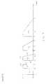
- FIG. 3a plurality of programming signals ( 200 , 201 , 202 , 203 ) in accordance with an embodiment of the present invention are illustrated.
- different times T 0 -T 11are denoted on a TIME axis and different currents I 0 and I 1 are denoted on a CURRENT axis.
- signals 200 - 203have leading portions that occur prior to or when the signals reach their maximum level (e.g., I 1 ), trailing portions that occur after the signals reach their maximum level, and intermediate portions between the leading and trailing portions.
- signal 200has a leading portion 211 , an intermediate portion 212 , and a trailing portion 213 and signal 201 has a leading portion 215 , an intermediate portion 216 , and a trailing portion 217 .
- signals 200 - 203are current pulses having different fall times.
- the fall time of a signalmay be defined as the time that the trailing portion decreases from a maximum level to a minimum level. In alternate embodiments, the fall time may be defined as the time that the trailing portion decreases from 90% of the maximum level to 10% of the maximum level.
- the fall time of signal 201is the time it takes for trailing portion 217 to decrease from a maximum current amplitude of I 1 to a minimum current amplitude of I 0 , that is, the fall time is the difference between times T 5 and T 4 .
- signal 200may have a fall time of substantially zero since the trailing portion of signal 200 decreases from its maximum amplitude (I 1 ) to its minimum amplitude (I 0 ) at time T 2 .
- Signal 200is a substantially rectangular pulse and signals 201 , 202 , and 203 are substantially nonrectangular pulses. Pulses 201 , 202 , and 203 may also be referred to as triangular pulses. Pulses 200 , 201 , 202 , and 203 have successively greater fall times. That is, signal 201 has a fall time greater than the fall time of signal 200 and less than the fall time of signal 202 , and signal 203 has a fall time greater than the fall time of signal 202 .
- signal 200may have rise and fall times of approximately zero (e.g., less than 2 nanoseconds), and may have a maximum current amplitude (e.g., I 1 ) of approximately 3 milliamps.
- Signal 201may have a maximum current amplitude of approximately 3 milliamps, a rise time of approximately zero, and a fall time (T 5 ⁇ T 4 ) of approximately 250 nanoseconds.
- Signal 202may have a maximum current amplitude of approximately 3 milliamps, a rise time of approximately zero, and a fall time (T 8 ⁇ T 7 ) of approximately 700 nanoseconds.
- Signal 203may have a maximum current amplitude of approximately 3 milliamps, a rise time of approximately zero, and a fall time (T 11 ⁇ T 10 ) of approximately 2 microseconds.
- programming signal generator device 160may be adapted to generate programming signals 200 - 203 to apply to memory cells 140 - 143 .
- device 160may comprise a circuit to set the fall time of programming signals 200 - 203 .
- device 160may comprise a circuit to set the fall time of a programming signal by setting the decay rate of the programming signal.
- device 160may comprise a circuit to set the fall time of a programming signal by shaping a slope of a trailing portion of the programming signal.
- the decay ratemay be defined as the rate at which a trailing portion of a signal decreases from its maximum amplitude to its minimum amplitude, and may be measured in terms of current per unit of time for signals 200 - 203 .
- the decay rates of programming signals 200 - 203may be increased to reduce the fall time of these programming signals.
- the decay rates of programming signals 200 - 203may be decreased to increase the fall time of these programming signals.
- signal 201has a faster or greater decay rate than the decay rate of signal 202
- signal 202has a faster decay rate than the decay rate of signal 203 .
- the decay rate of a programming signalmay be polynomial, logarithmic, or exponential, etc., although the scope of the present invention is not limited in this respect.
- the slopes of leading portion 211 and trailing portion 213 of signal 200are set to be substantially vertical and the slope of intermediate portion 212 of signal 200 is set to be substantially horizontal.
- Signal 201has a leading portion 215 that is set to a substantially vertical slope, an intermediate portion 216 that is set to a substantially horizontal slope and a trailing portion that is set to a negative linear slope.
- a programming signalis shaped by setting the fall time so that the decaying or sloping trailing portion of the programming signal cools the phase change memory material at a rate sufficient to place the memory cell in a desired state of the multiple memory states.
- the fall time of the programming signal applied to a phase change materialmay be increased to reduce the resistance of the phase change material.
- the resulting resistance of the phase change materialis not determined by the amplitude of the programming signal, but rather by the fall time of the programming signal.
- device 160may set an amplitude of a programming signal to an amplitude sufficient to heat the phase change material of a memory cell to an amorphizing temperature and place the phase change material in a substantially amorphous state.
- the materialmay be rapidly cooled. This may be accomplished by having a relatively fast fall time for the applied programming signal.
- signal 200may be used to place the phase change material of a memory cell in a substantially amorphous state, and signal 200 may have a maximum amplitude (I 1 ) of approximately 3 milliamps and a fall time of less than 2 nanoseconds.
- device 160may set the amplitude of the programming signal to an amplitude sufficient to heat the phase change material to an amorphizing temperature, and set a fall time of the programming signal so that after the memory material reaches the amorphizing temperature, the phase change memory material may cool down at a sufficient rate so that the memory material may be placed in the polycrystalline state.
- signal 203may be used to place a phase change material of a memory cell in a polycrystalline state, wherein signal 203 may have a maximum amplitude (I 1 ) of approximately 3 milliamps and a fall time of approximately 2 microseconds.
- device 160may set the fall time of the programming signal so that after the memory material reaches the amorphizing temperature, the phase change material may cool down at a sufficient rate so that the memory material is placed in the intermediate state.
- signal 202may be used to place the phase change material of a memory cell in an intermediate state, wherein signal 202 may have a maximum amplitude (I 1 ) of approximately 3 milliamps and a fall time of approximately 700 nanoseconds.
- an overwrite operationmay be implemented by heating the phase change material to an amorphizing temperature during a write operation, then controlling the fall time (or decay rate or trailing portion slope) of the signal to place the phase change material in different states, e.g., either a substantially amorphous state, a polycrystalline state, or a heterogeneous state.
- Programming in this fashionmay allow for overwriting of the cell since the programming signal in this example may result in heating the phase change material to an amorphizing temperature, and depending on the fall time (or decay rate or slope of a trailing portion) of the signal, the material may either be placed in a substantially amorphous state, a substantially crystalline state, or an intermediate heterogeneous state.
- signals 200 - 203 to memory cells 140 - 143may heat and cool the phase change materials of memory cells 140 - 143 to set the resistance of the phase change materials, thereby setting the state of the associated memory cell.
- signals 200 - 203may be used to set the state of the phase change material in a particular memory cell to one of the more than two states.
- signal 200may be used to place the phase change material of memory cell 140 to a substantially amorphous state, e.g., state (0,0);
- signal 201may be used to place the phase change material of memory cell 140 in an intermediate state, e.g., state (0,1);
- signal 202may be used to place the phase change material of memory cell 140 in another intermediate state, e.g., state (1,0);
- signal 203may be used to place the phase change material of memory cell 140 in a substantially crystalline state, e.g., state (1,1).
- signals 200 - 203may be used to set the state of a memory cell using a feedback approach. For example, to set memory cell 140 to an intermediate state (1,0), signal 202 may be initially applied to memory cell 140 . Then, read device 150 may be used to perform a verify operation to determine if memory cell 140 was programmed to the selected state of (1,0). For example, read device 150 may measure the resistance of the phase change material of memory cell 140 , and compare this resistance to a reference resistance to determine if the resistance of the phase change material is above or below the target resistance.
- the resistance of the phase change materialmay be reduced by applying signal 203 that has a greater fall time than the fall time of signal 202 or the resistance of the phase change material may be increased by applying signal 201 that has a smaller fall time than the fall time of signal 202 .
- This iterative process of applying programming signals having different fall times to program memory cell 140 to one of at least three statesmay be repeated until the desired state (e.g., the desired resistance) of the phase change material is achieved.
- the actual temperature of the phase change material in an array of memory cellsmay vary from cell to cell for a given programming current signal. This variation may result in the phase change material in one or more of the memory cells to inadvertently program a memory cell to an erroneous state.
- variations in materials, manufacturing processes, and operating environmentmay result in different programming characteristics for the memory cells in a phase change memory, wherein the different programming characteristics include variations in resulting resistance of the phase change materials when a rectangular pulse having a predetermined amount of current is applied to these memory cells.
- the fall time of a programming signalmay be set so that that different memory cells having different programming characteristics (e.g., different resulting resistance vs. applied current) are placed in a selected state when the programming signal is applied to the different memory cells.
- the fall time of a programming signalmay be set so that all memory cells that the programming signal is applied, sweep through a rapid crystallization temperature interval.
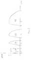
- FIGS. 4, 5 , and 6illustrate programming signals in accordance with other embodiments of the present invention.
- FIG. 4includes signals 400 , 401 , 402 , and 403 having successively greater fall times.
- signal 400may have a fall time of substantially zero.
- the fall time of signal 401may be greater than the fall time of signal 400 and less than the fall time of signal 402
- the fall time of signal 402may be less than the fall time of signal 403 .
- the slopes of the leading and trailing portions of signal 400may be substantially vertical and the slope of the intermediate portion of signal 400 may be substantially horizontal.
- Signal 401may have a leading portion that has a substantially vertical slope, an intermediate portion that has a substantially horizontal slope and a trailing portion having a negative nonlinear slope that varies with time.
- the slope of the trailing portion of signal 401may decrease with time.
- the slopes of the trailing portions of signals 402 and 403may decrease with time.
- FIG. 5includes signals 500 , 501 , 502 , and 503 having successively greater fall times.
- the slopes of the trailing portions of signals 501 , 502 , and 503are negative, nonlinear, and vary with time. In this embodiment, the slopes of the trailing portions of signals 501 , 502 , and 503 increase with time.
- the maximum amplitude (I 1 ) of signal 500is different compared to the maximum amplitudes (I 2 ) of signals 501 , 502 , and 503 .
- the maximum amplitude of signal 500may be approximately 3 milliamps and the maximum amplitudes of signals 501 , 502 , and 503 may be approximately 3.5 milliamps.
- FIG. 6includes signals 600 , 601 , 602 , and 603 having successively greater fall times.
- the slopes of the trailing portions of signals 601 - 603are negative and vary with time.
- the slopes of the trailing portions of signals 601 - 603change from a decreasing negative linear slope to a substantially vertical slope, e.g., the slope of the trailing portion of signal 601 decreases with time between times T 4 and T 5 and is substantially vertical at time T 5 .
- programming signals of FIGS. 4-6may be generated and applied in a similar manner to program memory cells 140 - 143 (FIG. 2) as the programming signals of FIG. 3, or any combination of the programming signals of FIGS. 3-6 may be used to program memory cells 140 - 143 .
- signal 200 , 401 , 502 , and 603having different fall times, may be used to program memory cells 140 - 143 to a desired state.
- programming signal generator device 160may generate any of the programming signals of FIGS. 3-6 and set the fall times of the programming signals to program the phase change memory material of memory cells 140 - 143 to one of at least three states.
- Programming signal generator device 160may include a circuit comprising a resistor and capacitor (not shown) to set the fall time of a programming signal.
- the resistor and capacitormay be chosen so that the resulting time constant of the resistor and capacitor sets the fall time of the programming signals.
- device 160may include a waveshaping circuit (not shown) comprising analog waveshaping circuits such as, for example, integrator/ramp circuits, exponential and logarithmic circuits, etc.
- Read device 150may include a circuit to read the information stored in the memory cells 140 - 143 .
- read device 150may include a circuit to route a current through memory cell 140 that results in a voltage developing across memory cell 140 . This voltage may be proportional to the resistance exhibited by the memory cell. Thus, a higher voltage may indicate that the cell is in an amorphous state, e.g., a higher resistance state; and a lower voltage may indicate that the cell is in a polycrystalline state, e.g., a lower resistance state.
- FIG. 7an embodiment of read device 150 in accordance with the present invention is provided.
- three comparators 711 , 712 , and 713may be used to detect a memory state of a particular memory cell, e.g., memory cell 140 .
- the noninverting input terminals of a comparators 711 - 713may be connected to memory cell 140 to receive an indication of the resistance of memory cell 140 .
- the inverting input terminals of comparators 711 , 712 , and 713may be connected to reference voltage signals REF 1 , REF 2 , and REF 3 , respectively.
- comparators 711 , 712 , and 713may be connected to the D input terminals of D flip-flops 721 , 722 , and 723 , respectively.
- a read current, labeled Icmay be used to generate a read voltage that may be received at the noninverting input terminals of comparators 711 - 713 .
- the read voltageis indicative of the resistance of memory cell 140 , and therefore, may be used to indicate the state of memory cell 140 .
- the comparison of the read voltage to the reference voltagesresults in output signals C 1 , C 2 , and C 3 that may be used to indicate the state of memory cell 140 and may be stored in flip-flops 721 - 723 .
- the output terminals of flip-flops 721 - 723may be connected to an encode circuit 730 that may generate signals OUT 1 and OUT 2 at its output terminals.
- Reference voltage signals REF 1 , REF 2 , and REF 3have the following voltage relationship: REF 1 >REF 2 >REF 3 .
- comparators 711 , 712 , and 713may respectively generate output signals C 1 , C 2 , and C 3 having a logic high voltage potential (“H”), and may be defined as state (0,0).
- comparators 711 , 712 , and 713may respectively generate output signals C 1 , C 2 , and C 3 having a logic low voltage potential (“L”) and may be defined as state (1,1).
- Llogic low voltage potential
- Timing device 170provides control signals to programming signal generator device 160 and read device 150 so that devices 150 and 160 either measure the resistance of a memory cell (read operation or program verify operation) or provide the programming pulses at the correct timing to the selected memory cell. Accesses to the memory cell may be in random fashion where a memory cell may be accessed individually, or it may be on a row by row basis.
- Embodiment 800may comprise a portable communication device 810 .
- Portable communication device 810may include a controller 820 , an input/output (I/O) device 830 (e.g. a keypad, display), a memory 840 , and a transceiver 850 that may be connected to an antennae 860 , although the scope of the present invention is not limited to embodiments having any or all of these components.
- I/Oinput/output
- Controller 820may comprise, for example, one or more microprocessors, digital signal processors, microcontrollers, or the like.
- Memory 840may be used to store messages transmitted to or by portable communication device 810 .
- Memory 840may also optionally be used to store instructions that are executed by controller 820 during the operation of portable communication device 810 , and may be used to store user data.
- Memory 840may be provided by one or more different types of memory.
- memory 840may comprise a volatile memory (any type of random access memory), a non-volatile memory such as a flash memory and/or a phase change memory such as, for example, phase change memory 33 illustrated in FIG. 2 .
- I/O device 830may be used by a user to generate a message.
- Portable communication device 810may use transceiver 850 with antennae 860 to transmit and receive messages to and from a wireless communication network with a radio frequency (RF) signal.
- RFradio frequency
- portable communication device 810may use one of the following communication protocols to transmit and receive messages: Code Division Multiple Access (CDMA), cellular radiotelephone communication systems, Global System for Mobile Communications (GSM) cellular radiotelephone systems, North American Digital Cellular (NADC) cellular radiotelephone systems, Time Division Multiple Access (TDMA) systems, Extended-TDMA (E-TDMA) cellular radiotelephone systems, third generation (3G) systems like Wide-band CDMA (WCDMA), CDMA-2000, and the like.
- CDMACode Division Multiple Access
- GSMGlobal System for Mobile Communications
- NADCNorth American Digital Cellular
- TDMATime Division Multiple Access
- E-TDMAExtended-TDMA
- 3Gthird generation
- WCDMAWide-band CDMA
- CDMA-2000Code Division Multiple Access-2000
Landscapes
- Engineering & Computer Science (AREA)
- Computer Hardware Design (AREA)
- Chemical & Material Sciences (AREA)
- Crystallography & Structural Chemistry (AREA)
- Semiconductor Memories (AREA)
- Circuits Of Receivers In General (AREA)
- Networks Using Active Elements (AREA)
- Stabilization Of Oscillater, Synchronisation, Frequency Synthesizers (AREA)
- Logic Circuits (AREA)
Abstract
Description
A phase change material may be used in a memory cell to store a bit of data. Phase change materials that are used in memory devices may exhibit at least two different states. These states may be referred to as the amorphous and crystalline states. These states may be distinguished because the amorphous state generally exhibits higher resistivity than the crystalline state. Generally, the amorphous state involves a more disordered atomic structure.
Rectangular current pulses may be used to program the phase change material to a desired state. The amplitude of the current pulse may be varied to change the resistance of the phase change material. However, variations in the materials, fabrication processes, and operating environment may cause the resulting resistance in different memory cells of a memory array to vary for a given rectangular current pulse. Thus, when programming multiple memory cells in a memory array, due to these variations, some cells may be programmed to one state, while others may be programmed to a different state when the same rectangular pulse is applied to each memory cell, or some cells while programmed to the desired state may not have adequate sense margins.
Thus, there is a continuing need for better ways to program memory cells in memory systems using phase change materials.
The subject matter regarded as the invention is particularly pointed out and distinctly claimed in the concluding portion of the specification. The invention, however, both as to organization and method of operation, together with objects, features, and advantages thereof, may best be understood by reference to the following detailed description when read with the accompanying drawings in which:
FIG. 1 is a block diagram of a computing system in accordance with an embodiment of the present invention;
FIG. 2 is schematic diagram of a phase change memory in accordance with an embodiment of the present invention;
FIG. 3 illustrates a plurality of programming signals in accordance with an embodiment of the present invention;
FIG. 4 illustrates another plurality of programming signals in accordance with another embodiment of the present invention;
FIG. 5 illustrates another plurality of programming signals in accordance with another embodiment of the present invention;
FIG. 6 illustrates yet another plurality of programming signals in accordance with another embodiment of the present invention;
FIG. 7 illustrates a read circuit in accordance with an embodiment of the present invention; and
FIG. 8 is a block diagram of a portable communication device in accordance with an embodiment of the present invention.
It will be appreciated that for simplicity and clarity of illustration, elements illustrated in the figures have not necessarily been drawn to scale. For example, the dimensions of some of the elements are exaggerated relative to other elements for clarity. Further, where considered appropriate, reference numerals have been repeated among the figures to indicate corresponding or analogous elements.
In the following detailed description, numerous specific details are set forth in order to provide a thorough understanding of the invention. However, it will be understood by those skilled in the art that the present invention may be practiced without these specific details. In other instances, well-known methods, procedures, components and circuits have not been described in detail so as not to obscure the present invention.
In the following description and claims, the terms “coupled” and “connected,” along with their derivatives, may be used. It should be understood that these terms are not intended as synonyms for each other. Rather, in particular embodiments, “connected” may be used to indicate that two or more elements are in direct physical or electrical contact with each other. “Coupled” may mean that two or more elements are in direct physical or electrical contact. However, “coupled” may also mean that two or more elements are not in direct contact with each other, but yet still co-operate or interact with each other.
Turning to FIG. 1, anembodiment 20 in accordance with the present invention is described.Embodiment 20 may comprise acomputing system 30.Computing system 30 may be used in a variety of portable electronic systems such as, for example, a portable communication device (e.g., a mobile cell phone), a two-way radio communication system, a one-way pager, a two-way pager, a personal communication system (PCS), a portable computer, a personal digital assistant (PDA), or the like. Although it should be pointed out that the scope and application of the present invention is in no way limited to these examples. For example, other applications where the present invention may be used are nonportable electronic applications, such as in cellular base stations, servers, desktop computers, video equipment, etc.
In this embodiment,computing system 30 may comprise aprocessor 42 that is connected to asystem bus 40. Although the scope of the present invention is not limited in this respect,processor 42 may comprise, for example, one or more microprocessors, digital signal processors, microcontrollers, or the like.System bus 40 may be a data path comprising, for example, a collection of data lines to transmit data from one part ofcomputing system 30 to another.
Memory controller hub34 may also be coupled to an input/output (I/O) hub52 via ahub interface 50. I/O hub52 may control operation of a CD-ROM drive 58 and may control operation of ahard disk drive 60. In addition, I/O hub52 may provide interfaces to, for example, a peripheral component interconnect (PCI) bus54 and anexpansion bus 62. PCI bus54 may be connected to a network interface card (NIC)56. An I/O controller 64 may be connected toexpansion bus 62 and may control operation of a floppy disk drive70. In addition, I/O controller 64 may receive input from amouse 66 and akeyboard 68.
Although the scope of the present invention is not limited in this respect,phase change memory 33 may be a memory array comprising a plurality of memory cells that may include a phase change memory material such as, for example, a chalcogenide material that may be programmed into different memory states to store data. This material may be, for example, a chalcogenide alloy that exhibits a reversible structural phase change from an amorphous state to a crystalline or a polycrystalline state. Due to the reversible structure, the phase change material may change from the amorphous state to the crystalline state and may revert back to the amorphous state thereafter, or vice versa, in response to temperature changes. A polycrystalline state may be defined as a state where multiple grain crystals are present with the possibility of some portions of the phase change material remaining amorphous.
A variety of phase change alloys may be used. For example, a chalcogenide alloy containing one or more elements from Column VI of the periodic table may be used inphase change memory 33. By way of example,phase change memory 33 may comprise GeSbTe alloys.
A volume of the chalcogenide alloy may be integrated into a memory cell to allow the cell to act as a nonvolatile programmable resistor, which reversibly changes between higher and lower resistance states. Crystallization in phase change materials may be a result of both the temperature and the amount of time the material spends at that temperature. Accordingly, the phase change may be induced by resistive heating using a current flowing through the phase change material. The programmable resistor may exhibit greater than 40 times dynamic range of resistivity between the crystalline state (low resistivity) and the amorphous state (high resistivity), and may also be capable of exhibiting multiple, intermediate states that allow multi-bit storage in a memory cell. The data stored in the cell may be read by measuring the cell's resistance.
By way of example, in a binary system storing one bit of data, a first state may be defined as the “1” state or set state and a second state may be defined as the “0” state or the reset state, wherein the reset state may be defined as a substantially amorphous state and the set state may be defined as a substantially crystalline state, although the scope of the present invention is not limited in this respect.
In multi level cell (MLC) operation, a phase change material may be used to exhibit multiple states to store multiple bits of data, wherein changing the state of a phase change memory material having more than two states may be accomplished by changing the resistivity/conductivity of the phase change material. For purposes of illustration, the embodiments herein describe binary systems that store 2-bits per memory cell using four states. A (0,0) state may be defined as a substantially amorphous (high resistivity) state; a (1,1) state may be defined as a substantially crystalline (low resistivity); and a (0,1) state and a (1,0) state may be intermediate states between the substantially amorphous and substantially crystalline states. These intermediate states may be referred to as heterogeneous states. As an example, the four states of the phase change material may be defined to have the following resistive relationship: the resistance of the phase change material in state (0,0) may be greater than the resistance of the phase change material in state (0,1); the resistance of the phase change material in state (0,1) may be greater than the resistance of the phase change material in state (1,0); and resistance of the phase change material in state (1,0) may be greater than the resistance of the phase change material in state (1,1). In other words, the conductivity of the phase change material in state (0,0) may be less than the conductivity of the phase change material in state (0,1), the conductivity of the phase change material in state (0,1) may be less than the conductivity of the phase change material in state (1,0), and conductivity of the phase change material in state (1,0) may be less than the conductivity of the phase change material in state (1,1).
Although a binary 2-bit per cell system is described for purposes of illustration, the scope of the present invention is not limited in this respect. The principles of the present invention may be similarly applicable to any system where the phase change memory material has more than two states. For example, in a nonbinary system, the memory states can be three or some other multiple of a nonbinary base.
Turning to FIG. 2, an embodiment ofphase change memory 33 in accordance with the present invention is described.Phase change memory 33 may include a 2×2array 139 ofmemory cells array 139 is illustrated in FIG. 2, the scope of the present invention is not limited in this respect. For example,phase change memory 33 may have a larger array of memory cells.
In this embodiment,phase change memory 33 further comprises a programmingsignal generator device 160 to perform a write operation, aread device 150 to perform a read operation, and atiming device 170 to generate timing signals to assist in the read and write operations. In MLC operation, readdevice 150 may also be used to verify status of memory cells140-143 during programming. For example, readdevice 150 may be used to determine whether the memory material in a memory cell is in a selected state of the more than two states after a programming signal is applied to the memory cell.
Programmingsignal generator device 160 may be adapted to generate programming signals to apply to memory cells140-143. For example,device 160 may be adapted to generate and apply the programming signals illustrated in FIGS. 3-6.
Turning to FIG. 3, a plurality of programming signals (200,201,202,203) in accordance with an embodiment of the present invention are illustrated. In FIG. 3, different times T0-T11are denoted on a TIME axis and different currents I0and I1are denoted on a CURRENT axis.
In this embodiment, signals200-203 have leading portions that occur prior to or when the signals reach their maximum level (e.g., I1), trailing portions that occur after the signals reach their maximum level, and intermediate portions between the leading and trailing portions. For example, signal200 has a leadingportion 211, anintermediate portion 212, and a trailing portion213 and signal201 has a leadingportion 215, anintermediate portion 216, and a trailingportion 217.
In this embodiment, signals200-203 are current pulses having different fall times. The fall time of a signal may be defined as the time that the trailing portion decreases from a maximum level to a minimum level. In alternate embodiments, the fall time may be defined as the time that the trailing portion decreases from 90% of the maximum level to 10% of the maximum level. As an example, the fall time ofsignal 201 is the time it takes for trailingportion 217 to decrease from a maximum current amplitude of I1to a minimum current amplitude of I0, that is, the fall time is the difference between times T5and T4.
In this embodiment, signal200 may have a fall time of substantially zero since the trailing portion ofsignal 200 decreases from its maximum amplitude (I1) to its minimum amplitude (I0) at time T2. Signal200 is a substantially rectangular pulse and signals201,202, and203 are substantially nonrectangular pulses.Pulses Pulses signal 200 and less than the fall time ofsignal 202, and signal203 has a fall time greater than the fall time ofsignal 202. In this example, signal200 may have rise and fall times of approximately zero (e.g., less than 2 nanoseconds), and may have a maximum current amplitude (e.g., I1) of approximately 3 milliamps.Signal 201 may have a maximum current amplitude of approximately 3 milliamps, a rise time of approximately zero, and a fall time (T5−T4) of approximately 250 nanoseconds.Signal 202 may have a maximum current amplitude of approximately 3 milliamps, a rise time of approximately zero, and a fall time (T8−T7) of approximately 700 nanoseconds.Signal 203 may have a maximum current amplitude of approximately 3 milliamps, a rise time of approximately zero, and a fall time (T11−T10) of approximately 2 microseconds.
As mentioned above, programming signal generator device160 (FIG. 2) may be adapted to generate programming signals200-203 to apply to memory cells140-143. In some embodiments,device 160 may comprise a circuit to set the fall time of programming signals200-203. In alternate embodiments,device 160 may comprise a circuit to set the fall time of a programming signal by setting the decay rate of the programming signal. In other embodiments,device 160 may comprise a circuit to set the fall time of a programming signal by shaping a slope of a trailing portion of the programming signal.
The decay rate may be defined as the rate at which a trailing portion of a signal decreases from its maximum amplitude to its minimum amplitude, and may be measured in terms of current per unit of time for signals200-203. The decay rates of programming signals200-203 may be increased to reduce the fall time of these programming signals. Conversely, the decay rates of programming signals200-203 may be decreased to increase the fall time of these programming signals. In the embodiment illustrated in FIG. 3, signal201 has a faster or greater decay rate than the decay rate ofsignal 202, and signal202 has a faster decay rate than the decay rate ofsignal 203. In alternate embodiments, the decay rate of a programming signal may be polynomial, logarithmic, or exponential, etc., although the scope of the present invention is not limited in this respect.
In the embodiment illustrated in FIG. 3, the slopes of leadingportion 211 and trailing portion213 ofsignal 200 are set to be substantially vertical and the slope ofintermediate portion 212 ofsignal 200 is set to be substantially horizontal.Signal 201 has a leadingportion 215 that is set to a substantially vertical slope, anintermediate portion 216 that is set to a substantially horizontal slope and a trailing portion that is set to a negative linear slope.
According to an embodiment of the invention, a programming signal is shaped by setting the fall time so that the decaying or sloping trailing portion of the programming signal cools the phase change memory material at a rate sufficient to place the memory cell in a desired state of the multiple memory states. The fall time of the programming signal applied to a phase change material may be increased to reduce the resistance of the phase change material. Using this programming method, the resulting resistance of the phase change material is not determined by the amplitude of the programming signal, but rather by the fall time of the programming signal.
In some embodiments,device 160 may set an amplitude of a programming signal to an amplitude sufficient to heat the phase change material of a memory cell to an amorphizing temperature and place the phase change material in a substantially amorphous state. To keep the phase change material in the substantially amorphous state, the material may be rapidly cooled. This may be accomplished by having a relatively fast fall time for the applied programming signal. As an example, signal200 may be used to place the phase change material of a memory cell in a substantially amorphous state, and signal200 may have a maximum amplitude (I1) of approximately 3 milliamps and a fall time of less than 2 nanoseconds.
Alternatively, to place the phase change material in a polycrystalline state,device 160 may set the amplitude of the programming signal to an amplitude sufficient to heat the phase change material to an amorphizing temperature, and set a fall time of the programming signal so that after the memory material reaches the amorphizing temperature, the phase change memory material may cool down at a sufficient rate so that the memory material may be placed in the polycrystalline state. As an example, signal203 may be used to place a phase change material of a memory cell in a polycrystalline state, wherein signal203 may have a maximum amplitude (I1) of approximately 3 milliamps and a fall time of approximately 2 microseconds. In addition, to place the phase change material in an intermediate state between the substantially amorphous and polycrystalline states,device 160 may set the fall time of the programming signal so that after the memory material reaches the amorphizing temperature, the phase change material may cool down at a sufficient rate so that the memory material is placed in the intermediate state. As an example, signal202 may be used to place the phase change material of a memory cell in an intermediate state, wherein signal202 may have a maximum amplitude (I1) of approximately 3 milliamps and a fall time of approximately 700 nanoseconds.
To avoid erasing memory cells prior to a write operation, in some embodiments, an overwrite operation may be implemented by heating the phase change material to an amorphizing temperature during a write operation, then controlling the fall time (or decay rate or trailing portion slope) of the signal to place the phase change material in different states, e.g., either a substantially amorphous state, a polycrystalline state, or a heterogeneous state. Programming in this fashion may allow for overwriting of the cell since the programming signal in this example may result in heating the phase change material to an amorphizing temperature, and depending on the fall time (or decay rate or slope of a trailing portion) of the signal, the material may either be placed in a substantially amorphous state, a substantially crystalline state, or an intermediate heterogeneous state.
As may be appreciated from the preceding discussion, application of signals200-203 to memory cells140-143 may heat and cool the phase change materials of memory cells140-143 to set the resistance of the phase change materials, thereby setting the state of the associated memory cell. For MLC operation, wherein the phase change materials of memory cells140-143 have more than two states, signals200-203 may be used to set the state of the phase change material in a particular memory cell to one of the more than two states. For example, signal200 may be used to place the phase change material ofmemory cell 140 to a substantially amorphous state, e.g., state (0,0);, signal201 may be used to place the phase change material ofmemory cell 140 in an intermediate state, e.g., state (0,1); signal202 may be used to place the phase change material ofmemory cell 140 in another intermediate state, e.g., state (1,0); and signal203 may be used to place the phase change material ofmemory cell 140 in a substantially crystalline state, e.g., state (1,1).
In alternate embodiments, signals200-203 may be used to set the state of a memory cell using a feedback approach. For example, to setmemory cell 140 to an intermediate state (1,0), signal202 may be initially applied tomemory cell 140. Then, readdevice 150 may be used to perform a verify operation to determine ifmemory cell 140 was programmed to the selected state of (1,0). For example, readdevice 150 may measure the resistance of the phase change material ofmemory cell 140, and compare this resistance to a reference resistance to determine if the resistance of the phase change material is above or below the target resistance. After applyingsignal 202, the resistance of the phase change material may be reduced by applyingsignal 203 that has a greater fall time than the fall time ofsignal 202 or the resistance of the phase change material may be increased by applyingsignal 201 that has a smaller fall time than the fall time ofsignal 202. This iterative process of applying programming signals having different fall times to programmemory cell 140 to one of at least three states may be repeated until the desired state (e.g., the desired resistance) of the phase change material is achieved.
Because of fabrication process and material variations in phase change memories, the actual temperature of the phase change material in an array of memory cells may vary from cell to cell for a given programming current signal. This variation may result in the phase change material in one or more of the memory cells to inadvertently program a memory cell to an erroneous state. In other words, variations in materials, manufacturing processes, and operating environment may result in different programming characteristics for the memory cells in a phase change memory, wherein the different programming characteristics include variations in resulting resistance of the phase change materials when a rectangular pulse having a predetermined amount of current is applied to these memory cells. In some embodiments, the fall time of a programming signal may be set so that that different memory cells having different programming characteristics (e.g., different resulting resistance vs. applied current) are placed in a selected state when the programming signal is applied to the different memory cells. In particular, the fall time of a programming signal may be set so that all memory cells that the programming signal is applied, sweep through a rapid crystallization temperature interval.
FIGS. 4,5, and6 illustrate programming signals in accordance with other embodiments of the present invention. FIG. 4 includessignals signal 401 may be greater than the fall time ofsignal 400 and less than the fall time ofsignal 402, and the fall time ofsignal 402 may be less than the fall time ofsignal 403. In this embodiment, the slopes of the leading and trailing portions ofsignal 400 may be substantially vertical and the slope of the intermediate portion ofsignal 400 may be substantially horizontal.Signal 401 may have a leading portion that has a substantially vertical slope, an intermediate portion that has a substantially horizontal slope and a trailing portion having a negative nonlinear slope that varies with time. In particular, the slope of the trailing portion ofsignal 401 may decrease with time. Similarly, the slopes of the trailing portions ofsignals
FIG. 5 includessignals signals signals signal 500 is different compared to the maximum amplitudes (I2) ofsignals signal 500 may be approximately 3 milliamps and the maximum amplitudes ofsignals
FIG. 6 includessignals
Although the scope of the present invention is not limited in this respect, it should be pointed that that the programming signals of FIGS. 4-6 may be generated and applied in a similar manner to program memory cells140-143 (FIG. 2) as the programming signals of FIG. 3, or any combination of the programming signals of FIGS. 3-6 may be used to program memory cells140-143. For example, signal200,401,502, and603, having different fall times, may be used to program memory cells140-143 to a desired state. Generally, for MLC operation, programming signal generator device160 (FIG. 2) may generate any of the programming signals of FIGS. 3-6 and set the fall times of the programming signals to program the phase change memory material of memory cells140-143 to one of at least three states.
Programmingsignal generator device 160 may include a circuit comprising a resistor and capacitor (not shown) to set the fall time of a programming signal. The resistor and capacitor may be chosen so that the resulting time constant of the resistor and capacitor sets the fall time of the programming signals. In alternate embodiments,device 160 may include a waveshaping circuit (not shown) comprising analog waveshaping circuits such as, for example, integrator/ramp circuits, exponential and logarithmic circuits, etc.
Read device150 (FIG. 2) may include a circuit to read the information stored in the memory cells140-143. As an example, readdevice 150 may include a circuit to route a current throughmemory cell 140 that results in a voltage developing acrossmemory cell 140. This voltage may be proportional to the resistance exhibited by the memory cell. Thus, a higher voltage may indicate that the cell is in an amorphous state, e.g., a higher resistance state; and a lower voltage may indicate that the cell is in a polycrystalline state, e.g., a lower resistance state.
Turning to FIG. 7, an embodiment ofread device 150 in accordance with the present invention is provided. For binary MLC operation, threecomparators memory cell 140. The noninverting input terminals of a comparators711-713 may be connected tomemory cell 140 to receive an indication of the resistance ofmemory cell 140. The inverting input terminals ofcomparators comparators flops memory cell 140, and therefore, may be used to indicate the state ofmemory cell 140.
The comparison of the read voltage to the reference voltages results in output signals C1, C2, and C3 that may be used to indicate the state ofmemory cell 140 and may be stored in flip-flops721-723. The output terminals of flip-flops721-723 may be connected to an encodecircuit 730 that may generate signals OUT1 and OUT2 at its output terminals.
Reference voltage signals REF1, REF2, and REF3 have the following voltage relationship: REF1>REF2>REF3. As a result of this arrangement, for a relatively higher resistive amorphous state ofmemory cell 140,comparators memory cell 140,comparators
| C1 | C2 | C3 | OUT1 | OUT2 | State | ||
| L | L | L | 1 | 1 | (1, 1) | ||
| H | L | L | 1 | 0 | (1, 0) | ||
| H | H | L | 0 | 1 | (0, 1) | ||
| H | H | H | 0 | 0 | (0, 0) | ||
The timing associated with the generation of the programming signals may be determined by timing device170 (FIG.2).Timing device 170 provides control signals to programmingsignal generator device 160 and readdevice 150 so thatdevices
Turning to FIG. 8, anembodiment 800 in accordance with the present invention is described.Embodiment 800 may comprise aportable communication device 810.Portable communication device 810 may include acontroller 820, an input/output (I/O) device830 (e.g. a keypad, display), amemory 840, and atransceiver 850 that may be connected to anantennae 860, although the scope of the present invention is not limited to embodiments having any or all of these components.
I/O device 830 may be used by a user to generate a message.Portable communication device 810 may usetransceiver 850 withantennae 860 to transmit and receive messages to and from a wireless communication network with a radio frequency (RF) signal.
Although the scope of the present invention is not limited in this respect,portable communication device 810 may use one of the following communication protocols to transmit and receive messages: Code Division Multiple Access (CDMA), cellular radiotelephone communication systems, Global System for Mobile Communications (GSM) cellular radiotelephone systems, North American Digital Cellular (NADC) cellular radiotelephone systems, Time Division Multiple Access (TDMA) systems, Extended-TDMA (E-TDMA) cellular radiotelephone systems, third generation (3G) systems like Wide-band CDMA (WCDMA), CDMA-2000, and the like.
While certain features of the invention have been illustrated and described herein, many modifications, substitutions, changes, and equivalents will now occur to those skilled in the art. It is, therefore, to be understood that the appended claims are intended to cover all such modifications and changes as fall within the true spirit of the invention.
Claims (37)
1. A method, comprising:
applying a signal to a memory material having more than two states; and
setting a fall time of the signal to place the memory material in one of the more than two states.
2. The method ofclaim 1 , further comprising increasing the fall time to reduce a resistance of the memory material.
3. The method ofclaim 1 , wherein setting the fall time includes setting the fall time of the signal to a first selected fall time to place the material in a first state of the more than two states, and the method further comprises:
setting the fall time of the signal to a second selected fall time to place the memory material in a second state of the more than two states;
setting the fall time of the signal to a third selected fall time to place the memory material in a third state of the more than two states; and
setting the fall time of signal to a fourth selected fall time to place the memory material in a fourth state of the more than two states.
4. The method ofclaim 3 , wherein the first selected fall time is less than the second selected fall time, the second selected fall time is less than the third selected fall time, and the third selected fall time is less than the fourth selected fall time.
5. The method ofclaim 3 , wherein a conductivity of the memory material in the first state is less than a conductivity of the material in the second state, a conductivity of the memory material in the second state is less than a conductivity of the material in the third state, and a conductivity of the memory material in the third state is less than a conductivity of the material in the fourth state.
6. The method ofclaim 1 , further comprising setting an amplitude of the signal to heat the memory material to an amorphizing temperature when the signal is applied to the memory material and wherein the fall time is set so that after the memory material reaches the amorphizing temperature, the memory material cool downs at a sufficient rate so that the memory material is placed in a first state of the more than two states, wherein the first state is a polycrystalline state.
7. The method ofclaim 1 , wherein applying a signal includes applying a pulse having a leading portion that occurs prior to the signal reaching a maximum level and a trailing portion that occurs after the signal reaches the maximum level and wherein the fall time is the time for the trailing portion to decrease from the maximum level to the minimum level.
8. The method ofclaim 1 , wherein setting the fall time of the signal comprises setting a slope of a trailing portion of the signal.
9. The method ofclaim 8 , wherein setting the slope comprises setting the slope of the trailing portion to a negative slope.
10. The method ofclaim 8 , wherein setting the slope includes setting a slope that varies with time.
11. The method ofclaim 8 , wherein setting the slope comprises shaping the trailing portion to change from a negative slope to a substantially vertical slope.
12. The method ofclaim 8 , wherein setting the slope comprises shaping the signal so that the signal is nonrectangular.
13. The method ofclaim 1 , wherein setting the fall time includes setting a decay rate of the signal.
14. The method ofclaim 13 , further comprising increasing the decay rate of the signal to reduce the fall time of the signal.
15. The method ofclaim 1 , wherein the memory material is a phase change material.
16. The method ofclaim 1 , further comprising applying a second signal to the memory material and applying a third signal to the memory material, wherein setting the fall time includes setting the fall time to be greater than a fall time of the second signal and less than a fall time of the third signal.
17. The method ofclaim 16 , wherein the signal places the memory material in a first state of the more than two memory states when the signal is applied to the memory material, the second signal places the memory material in a second state of the more than two memory states when the second signal is applied to the memory material and wherein the third signal places the memory material in a third state of the more than two memory states when the third signal is applied to the memory material.
18. The method ofclaim 17 , wherein the second state is a substantially amorphous state, the third state is a substantially crystalline state, and the first state is an intermediate state between the second and third states.
19. The method ofclaim 17 , wherein a resistance of the memory material in the second state is greater than the resistance of the memory material in the first state and the resistance of the memory material in the first state is greater than the resistance of the memory material in the third state.
20. The method ofclaim 1 , further comprising determining whether the memory material is in a selected state of the more than two states after the signal is applied to the memory.
21. The method ofclaim 20 , wherein determining comprises comparing a resistance of the memory material to a reference resistance.
22. The method ofclaim 20 , further comprising:
applying a second signal to the memory material if the memory material is not in the selected state, and
setting a fall time of the second signal to be greater than the fall time of the signal.
23. An apparatus, comprising:
a memory material having at least three states; and
a device to provide a signal to the memory material, wherein the device is adapted to set a fall time of the signal to program the memory material to one of the at least three states.
24. The apparatus ofclaim 23 , wherein the device sets the fall time of the signal to a first selected fall time to program the memory material to a first state of the at least three states, the device sets the fall time of the signal to a second selected fall time to program the memory material to a second state of the at least three states, and the device sets the fall time of the signal to a third selected fall time to program the memory material to a third state of the at least three states.
25. The apparatus ofclaim 24 , wherein the first selected fall time is less than the second selected fall time and the second selected fall time is less than the third selected fall time.
26. The apparatus ofclaim 24 , wherein a resistance of the memory material in the first state is greater than the resistance of the memory material in the second state and the resistance of the memory material in the second state is greater than the resistance of the memory material in the third state.
27. The apparatus ofclaim 23 , wherein the memory material is a phase change material.
28. The apparatus ofclaim 23 , wherein the device increases the fall time to reduce a resistance of the memory material.
29. The apparatus ofclaim 23 , wherein the device comprises a circuit to set the fall time of the signal by shaping a slope of a trailing portion of the signal.
30. The apparatus ofclaim 23 , wherein the device comprises a circuit to set the fall time of the signal by setting a decay rate of the signal.
31. The apparatus ofclaim 23 , wherein the device sets a fall time of the signal to program the memory material to a selected state of the at least three states and further comprising a circuit to determine whether the memory material is programmed to the selected state.
32. The apparatus ofclaim 31 , wherein the circuit comprises:
a comparator having a first input coupled to the memory material and a second input coupled to receive a first reference signal and an output; and
a second comparator having a first input coupled to the memory material and a second input coupled to receive a second reference signal and an output.
33. The apparatus ofclaim 23 , wherein the device is a circuit.
34. A system, comprising:
a controller;
a transceiver coupled to the controller;
a memory element having at least three states and coupled to the controller; and
a device adapted to provide a signal to the memory element, wherein the device sets a decay rate of the signal to program the memory element to one of the at least three states.
35. The system ofclaim 34 , wherein the device sets the decay rate of the signal to a first selected decay rate to program the memory element to a first state of the at least three states, the device sets the decay rate of the signal to a second selected decay rate to program the memory element to a second state of the at least three states, and the device sets the decay rate of the signal to a third selected decay rate to program the memory element to a third state of the at least three states.
36. The apparatus ofclaim 35 , wherein the first selected decay rate is greater than the second selected decay rate and the second selected decay rate is greater than the third selected decay rate.
37. The apparatus ofclaim 36 , wherein a conductivity of the memory element in the first state is less than the conductivity of the memory element in the second state and the conductivity of the memory element in the second state is less than the conductivity of the memory element in the third state.
Priority Applications (9)
| Application Number | Priority Date | Filing Date | Title |
|---|---|---|---|
| US10/034,146US6625054B2 (en) | 2001-12-28 | 2001-12-28 | Method and apparatus to program a phase change memory |
| TW091135681ATWI260016B (en) | 2001-12-28 | 2002-12-10 | Method and apparatus to program a phase change memory |
| PCT/US2002/040994WO2003058633A1 (en) | 2001-12-28 | 2002-12-20 | Method and apparatus to program a phase change memory |
| KR1020047010061AKR100705867B1 (en) | 2001-12-28 | 2002-12-20 | Programming method, apparatus and system of phase change memory |
| CNB028263340ACN100449642C (en) | 2001-12-28 | 2002-12-20 | Method, apparatus and system for programming phase change memory |
| AT02806193TATE336068T1 (en) | 2001-12-28 | 2002-12-20 | METHOD AND DEVICE FOR PROGRAMMING A PHASE CHANGE MEMORY |
| DE60213875TDE60213875T2 (en) | 2001-12-28 | 2002-12-20 | METHOD AND DEVICE FOR PROGRAMMING A PHASE CHANGE MEMORY |
| AU2002367356AAU2002367356A1 (en) | 2001-12-28 | 2002-12-20 | Method and apparatus to program a phase change memory |
| EP02806193AEP1468421B1 (en) | 2001-12-28 | 2002-12-20 | Method and apparatus to program a phase change memory |
Applications Claiming Priority (1)
| Application Number | Priority Date | Filing Date | Title |
|---|---|---|---|
| US10/034,146US6625054B2 (en) | 2001-12-28 | 2001-12-28 | Method and apparatus to program a phase change memory |
Publications (2)
| Publication Number | Publication Date |
|---|---|
| US20030123277A1 US20030123277A1 (en) | 2003-07-03 |
| US6625054B2true US6625054B2 (en) | 2003-09-23 |
Family
ID=21874593
Family Applications (1)
| Application Number | Title | Priority Date | Filing Date |
|---|---|---|---|
| US10/034,146Expired - Fee RelatedUS6625054B2 (en) | 2001-12-28 | 2001-12-28 | Method and apparatus to program a phase change memory |
Country Status (9)
| Country | Link |
|---|---|
| US (1) | US6625054B2 (en) |
| EP (1) | EP1468421B1 (en) |
| KR (1) | KR100705867B1 (en) |
| CN (1) | CN100449642C (en) |
| AT (1) | ATE336068T1 (en) |
| AU (1) | AU2002367356A1 (en) |
| DE (1) | DE60213875T2 (en) |
| TW (1) | TWI260016B (en) |
| WO (1) | WO2003058633A1 (en) |
Cited By (134)
| Publication number | Priority date | Publication date | Assignee | Title |
|---|---|---|---|---|
| US20030096497A1 (en)* | 2001-11-19 | 2003-05-22 | Micron Technology, Inc. | Electrode structure for use in an integrated circuit |
| US20030198118A1 (en)* | 2001-08-02 | 2003-10-23 | Lowery Tyler A. | Method for reading a structural phase-change memory |
| US20030218904A1 (en)* | 2001-06-29 | 2003-11-27 | Lowrey Tyler A. | Programming a phase-change material memory |
| US20040007718A1 (en)* | 2001-08-30 | 2004-01-15 | Campbell Kristy A. | Stoichiometry for chalcogenide glasses useful for memory devices and method of formation |
| US20040027908A1 (en)* | 2002-08-09 | 2004-02-12 | Tsukasa Ooishi | Nonvolatile memory device suitable for cache memory |
| US20040043245A1 (en)* | 2002-08-29 | 2004-03-04 | Moore John T. | Method to control silver concentration in a resistance variable memory element |
| US20040053461A1 (en)* | 2002-08-29 | 2004-03-18 | Moore John T. | Graded GexSe100-x concentration in PCRAM |
| US20040114419A1 (en)* | 2002-12-13 | 2004-06-17 | Lowrey Tyler A. | Method and system to store information |
| US20040130598A1 (en)* | 2002-07-10 | 2004-07-08 | Canon Kabushiki Kaisha | Ink jet record head |
| US6791885B2 (en) | 2002-02-19 | 2004-09-14 | Micron Technology, Inc. | Programmable conductor random access memory and method for sensing same |
| US6809362B2 (en) | 2002-02-20 | 2004-10-26 | Micron Technology, Inc. | Multiple data state memory cell |
| US20040211957A1 (en)* | 2002-08-29 | 2004-10-28 | Moore John T. | Method and apparatus for controlling metal doping of a chalcogenide memory element |
| US6812087B2 (en) | 2002-01-31 | 2004-11-02 | Micron Technology, Inc. | Methods of forming non-volatile resistance variable devices and methods of forming silver selenide comprising structures |
| US6813178B2 (en) | 2003-03-12 | 2004-11-02 | Micron Technology, Inc. | Chalcogenide glass constant current device, and its method of fabrication and operation |
| US6833559B2 (en) | 2001-02-08 | 2004-12-21 | Micron Technology, Inc. | Non-volatile resistance variable device |
| US20040264234A1 (en)* | 2003-06-25 | 2004-12-30 | Moore John T. | PCRAM cell operation method to control on/off resistance variation |
| US6849868B2 (en) | 2002-03-14 | 2005-02-01 | Micron Technology, Inc. | Methods and apparatus for resistance variable material cells |
| US6855975B2 (en) | 2002-04-10 | 2005-02-15 | Micron Technology, Inc. | Thin film diode integrated with chalcogenide memory cell |
| US6858482B2 (en) | 2002-04-10 | 2005-02-22 | Micron Technology, Inc. | Method of manufacture of programmable switching circuits and memory cells employing a glass layer |
| US6858465B2 (en) | 2002-06-06 | 2005-02-22 | Micron Technology, Inc. | Elimination of dendrite formation during metal/chalcogenide glass deposition |
| US6864500B2 (en) | 2002-04-10 | 2005-03-08 | Micron Technology, Inc. | Programmable conductor memory cell structure |
| US6867064B2 (en) | 2002-02-15 | 2005-03-15 | Micron Technology, Inc. | Method to alter chalcogenide glass for improved switching characteristics |
| US6867996B2 (en) | 2002-08-29 | 2005-03-15 | Micron Technology, Inc. | Single-polarity programmable resistance-variable memory element |
| US6867114B2 (en) | 2002-08-29 | 2005-03-15 | Micron Technology Inc. | Methods to form a memory cell with metal-rich metal chalcogenide |
| US6873538B2 (en) | 2001-12-20 | 2005-03-29 | Micron Technology, Inc. | Programmable conductor random access memory and a method for writing thereto |
| US6878569B2 (en) | 2001-03-15 | 2005-04-12 | Micron Technology, Inc. | Agglomeration elimination for metal sputter deposition of chalcogenides |
| US6882578B2 (en) | 2002-01-04 | 2005-04-19 | Micron Technology, Inc. | PCRAM rewrite prevention |
| US6891749B2 (en) | 2002-02-20 | 2005-05-10 | Micron Technology, Inc. | Resistance variable ‘on ’ memory |
| US6890790B2 (en) | 2002-06-06 | 2005-05-10 | Micron Technology, Inc. | Co-sputter deposition of metal-doped chalcogenides |
| US6894304B2 (en) | 2001-08-27 | 2005-05-17 | Micron Technology, Inc. | Apparatus and method for dual cell common electrode PCRAM memory device |
| US6903361B2 (en) | 2003-09-17 | 2005-06-07 | Micron Technology, Inc. | Non-volatile memory structure |
| US20050162907A1 (en)* | 2004-01-28 | 2005-07-28 | Campbell Kristy A. | Resistance variable memory elements based on polarized silver-selenide network growth |
| US20050167689A1 (en)* | 2004-01-29 | 2005-08-04 | Campbell Kristy A. | Non-volatile zero field splitting resonance memory |
| US6937528B2 (en) | 2002-03-05 | 2005-08-30 | Micron Technology, Inc. | Variable resistance memory and method for sensing same |
| US20050195633A1 (en)* | 2004-03-05 | 2005-09-08 | Byung-Gil Choi | Method for programming phase-change memory array to set state and circuit of a phase-change memory device |
| US6949402B2 (en) | 2001-03-01 | 2005-09-27 | Micron Technology, Inc. | Method of forming a non-volatile resistance variable device |
| US6951805B2 (en) | 2001-08-01 | 2005-10-04 | Micron Technology, Inc. | Method of forming integrated circuitry, method of forming memory circuitry, and method of forming random access memory circuitry |
| US6955940B2 (en) | 2001-08-29 | 2005-10-18 | Micron Technology, Inc. | Method of forming chalcogenide comprising devices |
| US20050232014A1 (en)* | 2004-03-31 | 2005-10-20 | Infineon Technologies Ag | Write/delete process for resistive switching memory components |
| US6961277B2 (en) | 2003-07-08 | 2005-11-01 | Micron Technology, Inc. | Method of refreshing a PCRAM memory device |
| US20050247927A1 (en)* | 2002-07-10 | 2005-11-10 | Campbell Kristy A | Assemblies displaying differential negative resistance |
| US20050280987A1 (en)* | 2004-06-07 | 2005-12-22 | Kwitek Benjamin J | Phase change materials as a heat sink for computers |
| US6998697B2 (en) | 2001-08-29 | 2006-02-14 | Micron Technology, Inc. | Non-volatile resistance variable devices |
| US7002833B2 (en) | 2001-11-20 | 2006-02-21 | Micron Technology, Inc. | Complementary bit resistance memory sensor and method of operation |
| US7010644B2 (en) | 2002-08-29 | 2006-03-07 | Micron Technology, Inc. | Software refreshed memory device and method |
| US7018863B2 (en) | 2002-08-22 | 2006-03-28 | Micron Technology, Inc. | Method of manufacture of a resistance variable memory cell |
| US7022579B2 (en) | 2003-03-14 | 2006-04-04 | Micron Technology, Inc. | Method for filling via with metal |
| US7031181B1 (en)* | 2004-11-23 | 2006-04-18 | Infineon Technologies Ag | Multi-pulse reset write scheme for phase-change memories |
| US7049009B2 (en) | 2002-08-29 | 2006-05-23 | Micron Technology, Inc. | Silver selenide film stoichiometry and morphology control in sputter deposition |
| US7050327B2 (en) | 2003-04-10 | 2006-05-23 | Micron Technology, Inc. | Differential negative resistance memory |
| US20060109707A1 (en)* | 2004-11-23 | 2006-05-25 | Infineon Technologies North America Corp. | Energy adjusted write pulses in phase-change memories |
| US7061004B2 (en) | 2003-07-21 | 2006-06-13 | Micron Technology, Inc. | Resistance variable memory elements and methods of formation |
| US20060126380A1 (en)* | 2004-11-26 | 2006-06-15 | Renesas Technology Corp. | Semiconductor device |
| US7071021B2 (en) | 2001-05-11 | 2006-07-04 | Micron Technology, Inc. | PCRAM memory cell and method of making same |
| US20060169968A1 (en)* | 2005-02-01 | 2006-08-03 | Thomas Happ | Pillar phase change memory cell |
| US7087919B2 (en) | 2002-02-20 | 2006-08-08 | Micron Technology, Inc. | Layered resistance variable memory device and method of fabrication |
| US20060175596A1 (en)* | 2005-02-10 | 2006-08-10 | Thomas Happ | Phase change memory cell with high read margin at low power operation |
| US20060175599A1 (en)* | 2005-02-10 | 2006-08-10 | Infineon Technologies North America Corp. | Phase change memory cell with high read margin at low power operation |
| US20060175597A1 (en)* | 2005-02-10 | 2006-08-10 | Infineon Technologies North America Corp. | Phase change memory cell with high read margin at low power operation |
| US7094700B2 (en) | 2002-08-29 | 2006-08-22 | Micron Technology, Inc. | Plasma etching methods and methods of forming memory devices comprising a chalcogenide comprising layer received operably proximate conductive electrodes |
| US7098068B2 (en) | 2004-03-10 | 2006-08-29 | Micron Technology, Inc. | Method of forming a chalcogenide material containing device |
| US20060220071A1 (en)* | 2005-04-04 | 2006-10-05 | Kang Sang-Beom | Phase-change semiconductor memory device and method of programming the same |
| US20060239058A1 (en)* | 2005-04-22 | 2006-10-26 | Micron Technology, Inc. | Method and apparatus for accessing a memory array |
| US20060274574A1 (en)* | 2004-02-04 | 2006-12-07 | Byung-Gil Choi | Phase-change memory device and method of writing a phase-change memory device |
| US7151688B2 (en) | 2004-09-01 | 2006-12-19 | Micron Technology, Inc. | Sensing of resistance variable memory devices |
| US20070008769A1 (en)* | 2005-07-06 | 2007-01-11 | Samsung Electronics Co., Ltd. | Phase-changeable memory device and method of programming the same |
| US7190048B2 (en) | 2004-07-19 | 2007-03-13 | Micron Technology, Inc. | Resistance variable memory device and method of fabrication |
| US7209378B2 (en) | 2002-08-08 | 2007-04-24 | Micron Technology, Inc. | Columnar 1T-N memory cell structure |
| US7233520B2 (en) | 2005-07-08 | 2007-06-19 | Micron Technology, Inc. | Process for erasing chalcogenide variable resistance memory bits |
| US20070171705A1 (en)* | 2005-12-15 | 2007-07-26 | Parkinson Ward D | Writing phase change memories |
| US7251154B2 (en) | 2005-08-15 | 2007-07-31 | Micron Technology, Inc. | Method and apparatus providing a cross-point memory array using a variable resistance memory cell and capacitance |
| US7269079B2 (en) | 2005-05-16 | 2007-09-11 | Micron Technology, Inc. | Power circuits for reducing a number of power supply voltage taps required for sensing a resistive memory |
| US7274034B2 (en) | 2005-08-01 | 2007-09-25 | Micron Technology, Inc. | Resistance variable memory device with sputtered metal-chalcogenide region and method of fabrication |
| US7277313B2 (en) | 2005-08-31 | 2007-10-02 | Micron Technology, Inc. | Resistance variable memory element with threshold device and method of forming the same |
| US20070228513A1 (en)* | 2006-03-28 | 2007-10-04 | Min Kyu S | Probe-based memory |
| US7294527B2 (en) | 2002-08-29 | 2007-11-13 | Micron Technology Inc. | Method of forming a memory cell |
| US7304368B2 (en) | 2005-08-11 | 2007-12-04 | Micron Technology, Inc. | Chalcogenide-based electrokinetic memory element and method of forming the same |
| US20070278538A1 (en)* | 2006-06-02 | 2007-12-06 | Industrial Technologoy Research Institute | Phase change memory cell |
| US20070280023A1 (en)* | 2006-05-18 | 2007-12-06 | Thomas Happ | Phase change memory having temperature budget sensor |
| US20070297221A1 (en)* | 2006-06-19 | 2007-12-27 | Jan Boris Philipp | Memory cell programmed using a temperature controlled set pulse |
| US7317200B2 (en) | 2005-02-23 | 2008-01-08 | Micron Technology, Inc. | SnSe-based limited reprogrammable cell |
| US7317567B2 (en) | 2005-08-02 | 2008-01-08 | Micron Technology, Inc. | Method and apparatus for providing color changing thin film material |
| US20080025080A1 (en)* | 2006-07-27 | 2008-01-31 | Cswitch Corporation | Method and apparatus for programming phase change devices |
| US7326950B2 (en) | 2004-07-19 | 2008-02-05 | Micron Technology, Inc. | Memory device with switching glass layer |
| US7332735B2 (en) | 2005-08-02 | 2008-02-19 | Micron Technology, Inc. | Phase change memory cell and method of formation |
| US20080062751A1 (en)* | 2006-09-11 | 2008-03-13 | Samsung Electronics Co., Ltd. | Phase change random access memory device |
| US7354793B2 (en) | 2004-08-12 | 2008-04-08 | Micron Technology, Inc. | Method of forming a PCRAM device incorporating a resistance-variable chalocogenide element |
| US7365411B2 (en) | 2004-08-12 | 2008-04-29 | Micron Technology, Inc. | Resistance variable memory with temperature tolerant materials |
| US20080106928A1 (en)* | 2006-09-20 | 2008-05-08 | Thomas Happ | Energy adjusted write pulses in phase-change memory cells |
| US7374174B2 (en) | 2004-12-22 | 2008-05-20 | Micron Technology, Inc. | Small electrode for resistance variable devices |
| US20080123398A1 (en)* | 2006-11-28 | 2008-05-29 | Thomas Nirschl | Memory cell with trigger element |
| US20080130351A1 (en)* | 2006-12-04 | 2008-06-05 | Thomas Nirschi | Multi-bit resistive memory |
| US20080151613A1 (en)* | 2006-12-25 | 2008-06-26 | Industrial Technology Research Institute | Programming method for phase change memory |
| US7396699B2 (en) | 2001-08-29 | 2008-07-08 | Micron Technology, Inc. | Method of forming non-volatile resistance variable devices and method of forming a programmable memory cell of memory circuitry |
| US7427770B2 (en) | 2005-04-22 | 2008-09-23 | Micron Technology, Inc. | Memory array for increased bit density |
| US20080237566A1 (en)* | 2007-03-26 | 2008-10-02 | Samsung Electronics Co., Ltd. | Phase change memory device and method of fabricating the same |
| US20080248632A1 (en)* | 2007-04-06 | 2008-10-09 | Samsung Electronics Co., Ltd. | Methods of Fabricating Multi-Bit Phase-Change Memory Devices and Devices Formed Thereby |
| US20080266932A1 (en)* | 2007-04-30 | 2008-10-30 | Thomas Happ | Circuit for programming a memory element |
| US20080266942A1 (en)* | 2007-04-30 | 2008-10-30 | Samsung Electronics Co., Ltd. | Multiple level cell phase-change memory device having pre-reading operation resistance drift recovery, memory systems employing such devices and methods of reading memory devices |
| US20080285333A1 (en)* | 2004-03-26 | 2008-11-20 | Koninklijke Philips Electronics, N.V. | Electric Device Comprising Phase Change Material |
| US20080316804A1 (en)* | 2007-06-20 | 2008-12-25 | Samsung Electronics Co., Ltd. | Multiple level cell phase-change memory devices having controlled resistance drift parameter, memory systems employing such devices and methods of reading memory devices |
| US20090001336A1 (en)* | 2007-06-29 | 2009-01-01 | Nazmul Habib | Phase change material based temperature sensor |
| US20090016099A1 (en)* | 2007-07-12 | 2009-01-15 | Samsung Electronics Co., Ltd. | Multiple level cell phase-change memory devices having post-programming operation resistance drift saturation, memory systems employing such devices and methods of reading memory devices |
| US20090027943A1 (en)* | 2007-07-24 | 2009-01-29 | Thomas Nirschl | Resistive memory including bidirectional write operation |
| DE102008038371A1 (en) | 2007-08-24 | 2009-02-26 | Samsung Electronics Co., Ltd., Suwon | Variable resistance memory and operating method thereof |
| US20090073754A1 (en)* | 2007-09-13 | 2009-03-19 | Samsung Electronics Co., Ltd. | Multi-level phase change memory device, program method thereof, and method and system including the same |
| US20090080242A1 (en)* | 2007-09-26 | 2009-03-26 | Claudio Resta | Programming a multilevel phase change memory cell |
| CN100505089C (en)* | 2004-04-06 | 2009-06-24 | 旺宏电子股份有限公司 | Method, circuit and production method for storing data by using ferroelectric memory |
| US20090194758A1 (en)* | 2008-02-05 | 2009-08-06 | Macronix International Co., Ltd. | Heating center pcram structure and methods for making |
| US7579615B2 (en) | 2005-08-09 | 2009-08-25 | Micron Technology, Inc. | Access transistor for memory device |
| US7583551B2 (en) | 2004-03-10 | 2009-09-01 | Micron Technology, Inc. | Power management control and controlling memory refresh operations |
| US7663133B2 (en) | 2005-04-22 | 2010-02-16 | Micron Technology, Inc. | Memory elements having patterned electrodes and method of forming the same |
| US7723713B2 (en) | 2002-02-20 | 2010-05-25 | Micron Technology, Inc. | Layered resistance variable memory device and method of fabrication |
| US7773409B2 (en) | 2007-03-08 | 2010-08-10 | Industrial Technology Research Institute | Writing method and system for a phase change memory |
| US20100202195A1 (en)* | 2008-03-26 | 2010-08-12 | Micron Technology, Inc. | Phase change memory |
| US7778066B2 (en) | 2007-08-23 | 2010-08-17 | Samsung Electronics Co., Ltd. | Resistance variable memory device and programming method thereof |
| US20100218070A1 (en)* | 2009-02-24 | 2010-08-26 | International Business Machines Corporation | Lengthening life of a limited life memory |
| US20100214831A1 (en)* | 2009-02-26 | 2010-08-26 | Ho-Jung Kim | Memory device, memory system having the same, and programming method of a memory cell |
| US7791058B2 (en) | 2006-08-29 | 2010-09-07 | Micron Technology, Inc. | Enhanced memory density resistance variable memory cells, arrays, devices and systems including the same, and methods of fabrication |
| US20100246246A1 (en)* | 2009-03-26 | 2010-09-30 | Ho-Jung Kim | Memory device, memory system having the same, and programming method of a memory cell |
| US20110032752A1 (en)* | 2009-08-10 | 2011-02-10 | Ik-Soo Kim | Multi-Level Memory Device Using Resistance Material |
| US20110051504A1 (en)* | 2009-08-31 | 2011-03-03 | Sandisk 3D Llc | Creating short program pulses in asymmetric memory arrays |
| US20110051505A1 (en)* | 2009-08-31 | 2011-03-03 | Sandisk 3D Llc | Reducing programming time of a memory cell |
| US20110051506A1 (en)* | 2009-08-31 | 2011-03-03 | Sandisk 3D Llc | Flexible multi-pulse set operation for phase-change memories |
| US7903447B2 (en)* | 2006-12-13 | 2011-03-08 | Macronix International Co., Ltd. | Method, apparatus and computer program product for read before programming process on programmable resistive memory cell |
| US20110147695A1 (en)* | 2009-12-23 | 2011-06-23 | Jong-Won Sean Lee | Fabricating current-confining structures in phase change memory switch cells |
| US8077505B2 (en) | 2008-05-07 | 2011-12-13 | Macronix International Co., Ltd. | Bipolar switching of phase change device |
| US8134857B2 (en) | 2008-06-27 | 2012-03-13 | Macronix International Co., Ltd. | Methods for high speed reading operation of phase change memory and device employing same |
| US8467236B2 (en) | 2008-08-01 | 2013-06-18 | Boise State University | Continuously variable resistor |
| US8917534B2 (en)* | 2011-09-09 | 2014-12-23 | Intel Corporation | Path isolation in a memory device |
| US20160071584A1 (en)* | 2014-09-04 | 2016-03-10 | Micron Technology, Inc. | Operational signals generated from capacitive stored charge |
| TWI549229B (en)* | 2014-01-24 | 2016-09-11 | 旺宏電子股份有限公司 | Multiple phase change materials in a memory device for system on a chip application |
| US10593403B2 (en) | 2016-02-23 | 2020-03-17 | Hewlett Packard Enterprise Development Lp | Memristive arrays with a waveform generation device |
| US10622049B1 (en)* | 2017-04-28 | 2020-04-14 | SK Hynix Inc. | Electronic device including a semiconductor memory that includes a circuit for changing a waveform of a write pulse |
Families Citing this family (28)
| Publication number | Priority date | Publication date | Assignee | Title |
|---|---|---|---|---|
| US6768665B2 (en)* | 2002-08-05 | 2004-07-27 | Intel Corporation | Refreshing memory cells of a phase change material memory device |
| US6831856B2 (en)* | 2002-09-23 | 2004-12-14 | Ovonyx, Inc. | Method of data storage using only amorphous phase of electrically programmable phase-change memory element |
| US20040197947A1 (en)* | 2003-04-07 | 2004-10-07 | Fricke Peter J. | Memory-cell filament electrodes and methods |
| EP1489622B1 (en)* | 2003-06-16 | 2007-08-15 | STMicroelectronics S.r.l. | Writing circuit for a phase change memory device |
| KR100505701B1 (en)* | 2003-08-13 | 2005-08-03 | 삼성전자주식회사 | Programming method of reducing set time of Phase-Change memory and writing driver circuit thereof |
| DE102004039977B4 (en)* | 2003-08-13 | 2008-09-11 | Samsung Electronics Co., Ltd., Suwon | Programming method and driver circuit for a phase change memory cell |
| US7005665B2 (en)* | 2004-03-18 | 2006-02-28 | International Business Machines Corporation | Phase change memory cell on silicon-on insulator substrate |
| US20060056233A1 (en)* | 2004-09-10 | 2006-03-16 | Parkinson Ward D | Using a phase change memory as a replacement for a buffered flash memory |
| EP1729303B1 (en)* | 2005-06-03 | 2010-12-15 | STMicroelectronics Srl | Method for multilevel programming of phase change memory cells using a percolation algorithm |
| US7907435B2 (en)* | 2005-09-21 | 2011-03-15 | Renesas Electronics Corporation | Semiconductor device |
| KR100738092B1 (en) | 2006-01-05 | 2007-07-12 | 삼성전자주식회사 | Multi-Bit Operation Method of Phase Transition Memory Device |
| JP4191211B2 (en)* | 2006-07-07 | 2008-12-03 | エルピーダメモリ株式会社 | Nonvolatile memory and control method thereof |
| KR100801082B1 (en)* | 2006-11-29 | 2008-02-05 | 삼성전자주식회사 | Method of driving multilevel variable resistance memory device and multilevel variable resistance memory device |
| US7571901B2 (en)* | 2007-06-21 | 2009-08-11 | Qimonda North America Corp. | Circuit for programming a memory element |
| TWI517156B (en)* | 2008-02-29 | 2016-01-11 | Toshiba Kk | Semiconductor memory device |
| KR101057725B1 (en) | 2008-12-31 | 2011-08-18 | 주식회사 하이닉스반도체 | Multi-level cell data sensing device and method thereof |
| DE102009000124A1 (en)* | 2009-01-09 | 2010-07-15 | Forschungszentrum Jülich GmbH | Method for storing digital information and memory element |
| US8183565B2 (en)* | 2009-03-25 | 2012-05-22 | Ovonyx, Inc. | Programmable resistance memory array with dedicated test cell |
| US8045384B2 (en)* | 2009-06-22 | 2011-10-25 | Sandisk Technologies Inc. | Reduced programming pulse width for enhanced channel boosting in non-volatile storage |
| TWI392514B (en) | 2010-01-29 | 2013-04-11 | Colgate Palmolive Co | A dentifrice with high microbial efficacy and no fluoride and anionic surfactant |
| KR101201839B1 (en) | 2010-04-26 | 2012-11-15 | 에스케이하이닉스 주식회사 | Semiconductor memory apparatus and method of generating programming current pulse |
| KR101201840B1 (en) | 2010-04-26 | 2012-11-15 | 에스케이하이닉스 주식회사 | Semiconductor memory apparatus |
| KR101216535B1 (en)* | 2011-04-27 | 2012-12-31 | 주식회사 메디칼써프라이 | A pulse oximeter using non-square waves |
| CN102543170B (en)* | 2012-02-17 | 2014-10-29 | 北京时代全芯科技有限公司 | Method for realizing low power consumption of phase change memory |
| US9786369B1 (en)* | 2015-04-10 | 2017-10-10 | Crossbar, Inc. | Enhanced MLC programming |
| KR102641097B1 (en)* | 2018-12-31 | 2024-02-27 | 삼성전자주식회사 | Resistive memory device and programming method of the same |
| US11812676B2 (en)* | 2020-03-24 | 2023-11-07 | International Business Machines Corporation | Multi-terminal phase change memory device |
| US11715517B2 (en) | 2021-08-06 | 2023-08-01 | International Business Machines Corporation | Linear phase change memory |
Citations (14)
| Publication number | Priority date | Publication date | Assignee | Title |
|---|---|---|---|---|
| US3271591A (en) | 1963-09-20 | 1966-09-06 | Energy Conversion Devices Inc | Symmetrical current controlling device |
| US3530441A (en) | 1969-01-15 | 1970-09-22 | Energy Conversion Devices Inc | Method and apparatus for storing and retrieving information |
| US5296716A (en) | 1991-01-18 | 1994-03-22 | Energy Conversion Devices, Inc. | Electrically erasable, directly overwritable, multibit single cell memory elements and arrays fabricated therefrom |
| US5789758A (en) | 1995-06-07 | 1998-08-04 | Micron Technology, Inc. | Chalcogenide memory cell with a plurality of chalcogenide electrodes |
| US5879955A (en) | 1995-06-07 | 1999-03-09 | Micron Technology, Inc. | Method for fabricating an array of ultra-small pores for chalcogenide memory cells |
| US5883827A (en)* | 1996-08-26 | 1999-03-16 | Micron Technology, Inc. | Method and apparatus for reading/writing data in a memory system including programmable resistors |
| US5933365A (en) | 1997-06-19 | 1999-08-03 | Energy Conversion Devices, Inc. | Memory element with energy control mechanism |
| US5970336A (en) | 1996-08-22 | 1999-10-19 | Micron Technology, Inc. | Method of making memory cell incorporating a chalcogenide element |
| US6031287A (en) | 1997-06-18 | 2000-02-29 | Micron Technology, Inc. | Contact structure and memory element incorporating the same |
| US6085341A (en) | 1996-12-31 | 2000-07-04 | Intel Corporation | Memory test mode for wordline resistive defects |
| US6087674A (en) | 1996-10-28 | 2000-07-11 | Energy Conversion Devices, Inc. | Memory element with memory material comprising phase-change material and dielectric material |
| US6141241A (en) | 1998-06-23 | 2000-10-31 | Energy Conversion Devices, Inc. | Universal memory element with systems employing same and apparatus and method for reading, writing and programming same |
| US6229157B1 (en) | 1996-06-18 | 2001-05-08 | Micron Technology, Inc. | Method of forming a polysilicon diode and devices incorporating such diode |
| US6487113B1 (en)* | 2001-06-29 | 2002-11-26 | Ovonyx, Inc. | Programming a phase-change memory with slow quench time |
Family Cites Families (5)
| Publication number | Priority date | Publication date | Assignee | Title |
|---|---|---|---|---|
| US4653024A (en)* | 1984-11-21 | 1987-03-24 | Energy Conversion Devices, Inc. | Data storage device including a phase changeable material |
| US4924436A (en)* | 1987-06-22 | 1990-05-08 | Energy Conversion Devices, Inc. | Data storage device having a phase change memory medium reversible by direct overwrite and method of direct overwrite |
| US5166758A (en)* | 1991-01-18 | 1992-11-24 | Energy Conversion Devices, Inc. | Electrically erasable phase change memory |
| US5687112A (en)* | 1996-04-19 | 1997-11-11 | Energy Conversion Devices, Inc. | Multibit single cell memory element having tapered contact |
| US5912839A (en)* | 1998-06-23 | 1999-06-15 | Energy Conversion Devices, Inc. | Universal memory element and method of programming same |
- 2001
- 2001-12-28USUS10/034,146patent/US6625054B2/ennot_activeExpired - Fee Related
- 2002
- 2002-12-10TWTW091135681Apatent/TWI260016B/ennot_activeIP Right Cessation
- 2002-12-20ATAT02806193Tpatent/ATE336068T1/ennot_activeIP Right Cessation
- 2002-12-20KRKR1020047010061Apatent/KR100705867B1/ennot_activeExpired - Fee Related
- 2002-12-20AUAU2002367356Apatent/AU2002367356A1/ennot_activeAbandoned
- 2002-12-20EPEP02806193Apatent/EP1468421B1/ennot_activeExpired - Lifetime
- 2002-12-20DEDE60213875Tpatent/DE60213875T2/ennot_activeExpired - Lifetime
- 2002-12-20CNCNB028263340Apatent/CN100449642C/ennot_activeExpired - Fee Related
- 2002-12-20WOPCT/US2002/040994patent/WO2003058633A1/enactiveIP Right Grant
Patent Citations (18)
| Publication number | Priority date | Publication date | Assignee | Title |
|---|---|---|---|---|
| US3271591A (en) | 1963-09-20 | 1966-09-06 | Energy Conversion Devices Inc | Symmetrical current controlling device |
| US3530441A (en) | 1969-01-15 | 1970-09-22 | Energy Conversion Devices Inc | Method and apparatus for storing and retrieving information |
| US5296716A (en) | 1991-01-18 | 1994-03-22 | Energy Conversion Devices, Inc. | Electrically erasable, directly overwritable, multibit single cell memory elements and arrays fabricated therefrom |
| US5789758A (en) | 1995-06-07 | 1998-08-04 | Micron Technology, Inc. | Chalcogenide memory cell with a plurality of chalcogenide electrodes |
| US5879955A (en) | 1995-06-07 | 1999-03-09 | Micron Technology, Inc. | Method for fabricating an array of ultra-small pores for chalcogenide memory cells |
| US5920788A (en) | 1995-06-07 | 1999-07-06 | Micron Technology, Inc. | Chalcogenide memory cell with a plurality of chalcogenide electrodes |
| US6002140A (en) | 1995-06-07 | 1999-12-14 | Micron Technology, Inc. | Method for fabricating an array of ultra-small pores for chalcogenide memory cells |
| US6229157B1 (en) | 1996-06-18 | 2001-05-08 | Micron Technology, Inc. | Method of forming a polysilicon diode and devices incorporating such diode |
| US5970336A (en) | 1996-08-22 | 1999-10-19 | Micron Technology, Inc. | Method of making memory cell incorporating a chalcogenide element |
| US5998244A (en) | 1996-08-22 | 1999-12-07 | Micron Technology, Inc. | Memory cell incorporating a chalcogenide element and method of making same |
| US6153890A (en) | 1996-08-22 | 2000-11-28 | Micron Technology, Inc. | Memory cell incorporating a chalcogenide element |
| US5883827A (en)* | 1996-08-26 | 1999-03-16 | Micron Technology, Inc. | Method and apparatus for reading/writing data in a memory system including programmable resistors |
| US6087674A (en) | 1996-10-28 | 2000-07-11 | Energy Conversion Devices, Inc. | Memory element with memory material comprising phase-change material and dielectric material |
| US6085341A (en) | 1996-12-31 | 2000-07-04 | Intel Corporation | Memory test mode for wordline resistive defects |
| US6031287A (en) | 1997-06-18 | 2000-02-29 | Micron Technology, Inc. | Contact structure and memory element incorporating the same |
| US5933365A (en) | 1997-06-19 | 1999-08-03 | Energy Conversion Devices, Inc. | Memory element with energy control mechanism |
| US6141241A (en) | 1998-06-23 | 2000-10-31 | Energy Conversion Devices, Inc. | Universal memory element with systems employing same and apparatus and method for reading, writing and programming same |
| US6487113B1 (en)* | 2001-06-29 | 2002-11-26 | Ovonyx, Inc. | Programming a phase-change memory with slow quench time |
Non-Patent Citations (2)
| Title |
|---|
| U.S. patent application, pending, Lowrey et al., 10/021,469, filed Oct. 30, 2001. |
| U.S. patent application, pending, Tyler Lowrey, 09/895,135, filed Jun. 29, 2001. |
Cited By (312)
| Publication number | Priority date | Publication date | Assignee | Title |
|---|---|---|---|---|
| US7030410B2 (en) | 2001-02-08 | 2006-04-18 | Micron Technology, Inc. | Resistance variable device |
| US6833559B2 (en) | 2001-02-08 | 2004-12-21 | Micron Technology, Inc. | Non-volatile resistance variable device |
| US6949402B2 (en) | 2001-03-01 | 2005-09-27 | Micron Technology, Inc. | Method of forming a non-volatile resistance variable device |
| US7199444B2 (en) | 2001-03-01 | 2007-04-03 | Micron Technology, Inc. | Memory device, programmable resistance memory cell and memory array |
| US7022555B2 (en) | 2001-03-01 | 2006-04-04 | Micron Technology, Inc. | Methods of forming a semiconductor memory device |
| US7528401B2 (en) | 2001-03-15 | 2009-05-05 | Micron Technology, Inc. | Agglomeration elimination for metal sputter deposition of chalcogenides |
| US6878569B2 (en) | 2001-03-15 | 2005-04-12 | Micron Technology, Inc. | Agglomeration elimination for metal sputter deposition of chalcogenides |
| US6974965B2 (en) | 2001-03-15 | 2005-12-13 | Micron Technology, Inc. | Agglomeration elimination for metal sputter deposition of chalcogenides |
| US6949453B2 (en) | 2001-03-15 | 2005-09-27 | Micron Technology, Inc. | Agglomeration elimination for metal sputter deposition of chalcogenides |
| US7071021B2 (en) | 2001-05-11 | 2006-07-04 | Micron Technology, Inc. | PCRAM memory cell and method of making same |
| US7687793B2 (en) | 2001-05-11 | 2010-03-30 | Micron Technology, Inc. | Resistance variable memory cells |
| US7235419B2 (en) | 2001-05-11 | 2007-06-26 | Micron Technology, Inc. | Method of making a memory cell |
| US6687153B2 (en)* | 2001-06-29 | 2004-02-03 | Ovonyx, Inc. | Programming a phase-change material memory |
| US20030218904A1 (en)* | 2001-06-29 | 2003-11-27 | Lowrey Tyler A. | Programming a phase-change material memory |
| US6951805B2 (en) | 2001-08-01 | 2005-10-04 | Micron Technology, Inc. | Method of forming integrated circuitry, method of forming memory circuitry, and method of forming random access memory circuitry |
| US6707712B2 (en)* | 2001-08-02 | 2004-03-16 | Intel Corporation | Method for reading a structural phase-change memory |
| US20030198118A1 (en)* | 2001-08-02 | 2003-10-23 | Lowery Tyler A. | Method for reading a structural phase-change memory |
| US6894304B2 (en) | 2001-08-27 | 2005-05-17 | Micron Technology, Inc. | Apparatus and method for dual cell common electrode PCRAM memory device |
| US6998697B2 (en) | 2001-08-29 | 2006-02-14 | Micron Technology, Inc. | Non-volatile resistance variable devices |
| US7863597B2 (en) | 2001-08-29 | 2011-01-04 | Micron Technology, Inc. | Resistance variable memory devices with passivating material |
| US6955940B2 (en) | 2001-08-29 | 2005-10-18 | Micron Technology, Inc. | Method of forming chalcogenide comprising devices |
| US7348205B2 (en) | 2001-08-29 | 2008-03-25 | Micron Technology, Inc. | Method of forming resistance variable devices |
| US7396699B2 (en) | 2001-08-29 | 2008-07-08 | Micron Technology, Inc. | Method of forming non-volatile resistance variable devices and method of forming a programmable memory cell of memory circuitry |
| US20040007718A1 (en)* | 2001-08-30 | 2004-01-15 | Campbell Kristy A. | Stoichiometry for chalcogenide glasses useful for memory devices and method of formation |
| US6888155B2 (en) | 2001-08-30 | 2005-05-03 | Micron Technology, Inc. | Stoichiometry for chalcogenide glasses useful for memory devices and method of formation |
| US6815818B2 (en)* | 2001-11-19 | 2004-11-09 | Micron Technology, Inc. | Electrode structure for use in an integrated circuit |
| US7115504B2 (en) | 2001-11-19 | 2006-10-03 | Micron Technology, Inc. | Method of forming electrode structure for use in an integrated circuit |
| US7115992B2 (en) | 2001-11-19 | 2006-10-03 | Micron Technology, Inc. | Electrode structure for use in an integrated circuit |
| US7332401B2 (en) | 2001-11-19 | 2008-02-19 | Micron Technology, Ing. | Method of fabricating an electrode structure for use in an integrated circuit |
| US20030096497A1 (en)* | 2001-11-19 | 2003-05-22 | Micron Technology, Inc. | Electrode structure for use in an integrated circuit |
| US7366003B2 (en) | 2001-11-20 | 2008-04-29 | Micron Technology, Inc. | Method of operating a complementary bit resistance memory sensor and method of operation |
| US7869249B2 (en) | 2001-11-20 | 2011-01-11 | Micron Technology, Inc. | Complementary bit PCRAM sense amplifier and method of operation |
| US7002833B2 (en) | 2001-11-20 | 2006-02-21 | Micron Technology, Inc. | Complementary bit resistance memory sensor and method of operation |
| US7242603B2 (en) | 2001-11-20 | 2007-07-10 | Micron Technology, Inc. | Method of operating a complementary bit resistance memory sensor |
| US6873538B2 (en) | 2001-12-20 | 2005-03-29 | Micron Technology, Inc. | Programmable conductor random access memory and a method for writing thereto |
| US6909656B2 (en) | 2002-01-04 | 2005-06-21 | Micron Technology, Inc. | PCRAM rewrite prevention |
| US6882578B2 (en) | 2002-01-04 | 2005-04-19 | Micron Technology, Inc. | PCRAM rewrite prevention |
| US7224632B2 (en) | 2002-01-04 | 2007-05-29 | Micron Technology, Inc. | Rewrite prevention in a variable resistance memory |
| US6812087B2 (en) | 2002-01-31 | 2004-11-02 | Micron Technology, Inc. | Methods of forming non-volatile resistance variable devices and methods of forming silver selenide comprising structures |
| US6867064B2 (en) | 2002-02-15 | 2005-03-15 | Micron Technology, Inc. | Method to alter chalcogenide glass for improved switching characteristics |
| US6954385B2 (en) | 2002-02-19 | 2005-10-11 | Micron Technology, Inc. | Method and apparatus for sensing resistive memory state |
| US6791885B2 (en) | 2002-02-19 | 2004-09-14 | Micron Technology, Inc. | Programmable conductor random access memory and method for sensing same |
| US7202520B2 (en) | 2002-02-20 | 2007-04-10 | Micron Technology, Inc. | Multiple data state memory cell |
| US7498231B2 (en) | 2002-02-20 | 2009-03-03 | Micron Technology, Inc. | Multiple data state memory cell |
| US6891749B2 (en) | 2002-02-20 | 2005-05-10 | Micron Technology, Inc. | Resistance variable ‘on ’ memory |
| US7087919B2 (en) | 2002-02-20 | 2006-08-08 | Micron Technology, Inc. | Layered resistance variable memory device and method of fabrication |
| US6809362B2 (en) | 2002-02-20 | 2004-10-26 | Micron Technology, Inc. | Multiple data state memory cell |
| US6908808B2 (en) | 2002-02-20 | 2005-06-21 | Micron Technology, Inc. | Method of forming and storing data in a multiple state memory cell |
| US8263958B2 (en) | 2002-02-20 | 2012-09-11 | Micron Technology, Inc. | Layered resistance variable memory device and method of fabrication |
| US7723713B2 (en) | 2002-02-20 | 2010-05-25 | Micron Technology, Inc. | Layered resistance variable memory device and method of fabrication |
| US6937528B2 (en) | 2002-03-05 | 2005-08-30 | Micron Technology, Inc. | Variable resistance memory and method for sensing same |
| US6849868B2 (en) | 2002-03-14 | 2005-02-01 | Micron Technology, Inc. | Methods and apparatus for resistance variable material cells |
| US7479650B2 (en) | 2002-04-10 | 2009-01-20 | Micron Technology, Inc. | Method of manufacture of programmable conductor memory |
| US7112484B2 (en) | 2002-04-10 | 2006-09-26 | Micron Technology, Inc. | Thin film diode integrated with chalcogenide memory cell |
| US6858482B2 (en) | 2002-04-10 | 2005-02-22 | Micron Technology, Inc. | Method of manufacture of programmable switching circuits and memory cells employing a glass layer |
| US6855975B2 (en) | 2002-04-10 | 2005-02-15 | Micron Technology, Inc. | Thin film diode integrated with chalcogenide memory cell |
| US7547905B2 (en) | 2002-04-10 | 2009-06-16 | Micron Technology, Inc. | Programmable conductor memory cell structure and method therefor |
| US6864500B2 (en) | 2002-04-10 | 2005-03-08 | Micron Technology, Inc. | Programmable conductor memory cell structure |
| US6890790B2 (en) | 2002-06-06 | 2005-05-10 | Micron Technology, Inc. | Co-sputter deposition of metal-doped chalcogenides |
| US7964436B2 (en) | 2002-06-06 | 2011-06-21 | Round Rock Research, Llc | Co-sputter deposition of metal-doped chalcogenides |
| US7202104B2 (en) | 2002-06-06 | 2007-04-10 | Micron Technology, Inc. | Co-sputter deposition of metal-doped chalcogenides |
| US7446393B2 (en) | 2002-06-06 | 2008-11-04 | Micron Technology, Inc. | Co-sputter deposition of metal-doped chalcogenides |
| US6858465B2 (en) | 2002-06-06 | 2005-02-22 | Micron Technology, Inc. | Elimination of dendrite formation during metal/chalcogenide glass deposition |
| US20040130598A1 (en)* | 2002-07-10 | 2004-07-08 | Canon Kabushiki Kaisha | Ink jet record head |
| US7879646B2 (en) | 2002-07-10 | 2011-02-01 | Micron Technology, Inc. | Assemblies displaying differential negative resistance, semiconductor constructions, and methods of forming assemblies displaying differential negative resistance |
| US7015494B2 (en) | 2002-07-10 | 2006-03-21 | Micron Technology, Inc. | Assemblies displaying differential negative resistance |
| US20050247927A1 (en)* | 2002-07-10 | 2005-11-10 | Campbell Kristy A | Assemblies displaying differential negative resistance |
| US7209378B2 (en) | 2002-08-08 | 2007-04-24 | Micron Technology, Inc. | Columnar 1T-N memory cell structure |
| US6778445B2 (en)* | 2002-08-09 | 2004-08-17 | Renesas Technology Corp. | Pipeline nonvolatile memory device with multi-bit parallel read and write suitable for cache memory. |
| US20040027908A1 (en)* | 2002-08-09 | 2004-02-12 | Tsukasa Ooishi | Nonvolatile memory device suitable for cache memory |
| US7459764B2 (en) | 2002-08-22 | 2008-12-02 | Micron Technology, Inc. | Method of manufacture of a PCRAM memory cell |
| US7018863B2 (en) | 2002-08-22 | 2006-03-28 | Micron Technology, Inc. | Method of manufacture of a resistance variable memory cell |
| US7550818B2 (en) | 2002-08-22 | 2009-06-23 | Micron Technology, Inc. | Method of manufacture of a PCRAM memory cell |
| US7364644B2 (en) | 2002-08-29 | 2008-04-29 | Micron Technology, Inc. | Silver selenide film stoichiometry and morphology control in sputter deposition |
| US7518212B2 (en) | 2002-08-29 | 2009-04-14 | Micron Technology, Inc. | Graded GexSe100-x concentration in PCRAM |
| US9552986B2 (en) | 2002-08-29 | 2017-01-24 | Micron Technology, Inc. | Forming a memory device using sputtering to deposit silver-selenide film |
| US6856002B2 (en) | 2002-08-29 | 2005-02-15 | Micron Technology, Inc. | Graded GexSe100-x concentration in PCRAM |
| US20040043245A1 (en)* | 2002-08-29 | 2004-03-04 | Moore John T. | Method to control silver concentration in a resistance variable memory element |
| US7087454B2 (en) | 2002-08-29 | 2006-08-08 | Micron Technology, Inc. | Fabrication of single polarity programmable resistance structure |
| US7056762B2 (en) | 2002-08-29 | 2006-06-06 | Micron Technology, Inc. | Methods to form a memory cell with metal-rich metal chalcogenide |
| US7564731B2 (en) | 2002-08-29 | 2009-07-21 | Micron Technology, Inc. | Software refreshed memory device and method |
| US7049009B2 (en) | 2002-08-29 | 2006-05-23 | Micron Technology, Inc. | Silver selenide film stoichiometry and morphology control in sputter deposition |
| US20040053461A1 (en)* | 2002-08-29 | 2004-03-18 | Moore John T. | Graded GexSe100-x concentration in PCRAM |
| US7094700B2 (en) | 2002-08-29 | 2006-08-22 | Micron Technology, Inc. | Plasma etching methods and methods of forming memory devices comprising a chalcogenide comprising layer received operably proximate conductive electrodes |
| US6864521B2 (en) | 2002-08-29 | 2005-03-08 | Micron Technology, Inc. | Method to control silver concentration in a resistance variable memory element |
| US20040211957A1 (en)* | 2002-08-29 | 2004-10-28 | Moore John T. | Method and apparatus for controlling metal doping of a chalcogenide memory element |
| US7010644B2 (en) | 2002-08-29 | 2006-03-07 | Micron Technology, Inc. | Software refreshed memory device and method |
| US6867114B2 (en) | 2002-08-29 | 2005-03-15 | Micron Technology Inc. | Methods to form a memory cell with metal-rich metal chalcogenide |
| US6953720B2 (en) | 2002-08-29 | 2005-10-11 | Micron Technology, Inc. | Methods for forming chalcogenide glass-based memory elements |
| US20050266635A1 (en)* | 2002-08-29 | 2005-12-01 | Moore John T | Graded GexSe100-x concentration in PCRAM |
| US6867996B2 (en) | 2002-08-29 | 2005-03-15 | Micron Technology, Inc. | Single-polarity programmable resistance-variable memory element |
| US7294527B2 (en) | 2002-08-29 | 2007-11-13 | Micron Technology Inc. | Method of forming a memory cell |
| US7944768B2 (en) | 2002-08-29 | 2011-05-17 | Micron Technology, Inc. | Software refreshed memory device and method |
| US20050148150A1 (en)* | 2002-08-29 | 2005-07-07 | Moore John T. | Memory element and its method of formation |
| US7768861B2 (en) | 2002-08-29 | 2010-08-03 | Micron Technology, Inc. | Software refreshed memory device and method |
| US7223627B2 (en) | 2002-08-29 | 2007-05-29 | Micron Technology, Inc. | Memory element and its method of formation |
| US7163837B2 (en) | 2002-08-29 | 2007-01-16 | Micron Technology, Inc. | Method of forming a resistance variable memory element |
| US7692177B2 (en) | 2002-08-29 | 2010-04-06 | Micron Technology, Inc. | Resistance variable memory element and its method of formation |
| US7307908B2 (en) | 2002-08-29 | 2007-12-11 | Micron Technology, Inc. | Software refreshed memory device and method |
| US6813177B2 (en)* | 2002-12-13 | 2004-11-02 | Ovoynx, Inc. | Method and system to store information |
| US20040114419A1 (en)* | 2002-12-13 | 2004-06-17 | Lowrey Tyler A. | Method and system to store information |
| US6813178B2 (en) | 2003-03-12 | 2004-11-02 | Micron Technology, Inc. | Chalcogenide glass constant current device, and its method of fabrication and operation |
| US7022579B2 (en) | 2003-03-14 | 2006-04-04 | Micron Technology, Inc. | Method for filling via with metal |
| US7745808B2 (en) | 2003-04-10 | 2010-06-29 | Micron Technology, Inc. | Differential negative resistance memory |
| US7329558B2 (en) | 2003-04-10 | 2008-02-12 | Micron Technology, Inc. | Differential negative resistance memory |
| US7050327B2 (en) | 2003-04-10 | 2006-05-23 | Micron Technology, Inc. | Differential negative resistance memory |
| US6930909B2 (en) | 2003-06-25 | 2005-08-16 | Micron Technology, Inc. | Memory device and methods of controlling resistance variation and resistance profile drift |
| US20040264234A1 (en)* | 2003-06-25 | 2004-12-30 | Moore John T. | PCRAM cell operation method to control on/off resistance variation |
| US7385868B2 (en) | 2003-07-08 | 2008-06-10 | Micron Technology, Inc. | Method of refreshing a PCRAM memory device |
| US6961277B2 (en) | 2003-07-08 | 2005-11-01 | Micron Technology, Inc. | Method of refreshing a PCRAM memory device |
| US7061004B2 (en) | 2003-07-21 | 2006-06-13 | Micron Technology, Inc. | Resistance variable memory elements and methods of formation |
| US6946347B2 (en) | 2003-09-17 | 2005-09-20 | Micron Technology, Inc. | Non-volatile memory structure |
| US7491963B2 (en) | 2003-09-17 | 2009-02-17 | Micron Technology, Inc. | Non-volatile memory structure |
| US6903361B2 (en) | 2003-09-17 | 2005-06-07 | Micron Technology, Inc. | Non-volatile memory structure |
| US7276722B2 (en) | 2003-09-17 | 2007-10-02 | Micron Technology, Inc. | Non-volatile memory structure |
| US20050286294A1 (en)* | 2004-01-28 | 2005-12-29 | Campbell Kristy A | Resistance variable memory elements based on polarized silver-selenide network growth |
| US20050162907A1 (en)* | 2004-01-28 | 2005-07-28 | Campbell Kristy A. | Resistance variable memory elements based on polarized silver-selenide network growth |
| US7153721B2 (en) | 2004-01-28 | 2006-12-26 | Micron Technology, Inc. | Resistance variable memory elements based on polarized silver-selenide network growth |
| US7105864B2 (en) | 2004-01-29 | 2006-09-12 | Micron Technology, Inc. | Non-volatile zero field splitting resonance memory |
| US20050167689A1 (en)* | 2004-01-29 | 2005-08-04 | Campbell Kristy A. | Non-volatile zero field splitting resonance memory |
| US20060274574A1 (en)* | 2004-02-04 | 2006-12-07 | Byung-Gil Choi | Phase-change memory device and method of writing a phase-change memory device |
| US7502251B2 (en)* | 2004-02-04 | 2009-03-10 | Samsung Electronics Co., Ltd. | Phase-change memory device and method of writing a phase-change memory device |
| US20050195633A1 (en)* | 2004-03-05 | 2005-09-08 | Byung-Gil Choi | Method for programming phase-change memory array to set state and circuit of a phase-change memory device |
| US7274586B2 (en)* | 2004-03-05 | 2007-09-25 | Samsung Electronics Co., Ltd. | Method for programming phase-change memory array to set state and circuit of a phase-change memory device |
| US7583551B2 (en) | 2004-03-10 | 2009-09-01 | Micron Technology, Inc. | Power management control and controlling memory refresh operations |
| US9142263B2 (en) | 2004-03-10 | 2015-09-22 | Round Rock Research, Llc | Power management control and controlling memory refresh operations |
| US7459336B2 (en) | 2004-03-10 | 2008-12-02 | Micron Technology, Inc. | Method of forming a chalcogenide material containing device |
| US7098068B2 (en) | 2004-03-10 | 2006-08-29 | Micron Technology, Inc. | Method of forming a chalcogenide material containing device |
| US8619485B2 (en) | 2004-03-10 | 2013-12-31 | Round Rock Research, Llc | Power management control and controlling memory refresh operations |
| US8115239B2 (en) | 2004-03-26 | 2012-02-14 | Nxp B.V. | Electric device comprising phase change material |
| US20080285333A1 (en)* | 2004-03-26 | 2008-11-20 | Koninklijke Philips Electronics, N.V. | Electric Device Comprising Phase Change Material |
| US7457145B2 (en)* | 2004-03-31 | 2008-11-25 | Infineon Technologies Ag | Write/delete process for resistive switching memory components |
| US20050232014A1 (en)* | 2004-03-31 | 2005-10-20 | Infineon Technologies Ag | Write/delete process for resistive switching memory components |
| CN100505089C (en)* | 2004-04-06 | 2009-06-24 | 旺宏电子股份有限公司 | Method, circuit and production method for storing data by using ferroelectric memory |
| US20050280987A1 (en)* | 2004-06-07 | 2005-12-22 | Kwitek Benjamin J | Phase change materials as a heat sink for computers |
| US7749853B2 (en) | 2004-07-19 | 2010-07-06 | Microntechnology, Inc. | Method of forming a variable resistance memory device comprising tin selenide |
| US7348209B2 (en) | 2004-07-19 | 2008-03-25 | Micron Technology, Inc. | Resistance variable memory device and method of fabrication |
| US7326950B2 (en) | 2004-07-19 | 2008-02-05 | Micron Technology, Inc. | Memory device with switching glass layer |
| US7190048B2 (en) | 2004-07-19 | 2007-03-13 | Micron Technology, Inc. | Resistance variable memory device and method of fabrication |
| US7759665B2 (en) | 2004-07-19 | 2010-07-20 | Micron Technology, Inc. | PCRAM device with switching glass layer |
| US7282783B2 (en) | 2004-07-19 | 2007-10-16 | Micron Technology, Inc. | Resistance variable memory device and method of fabrication |
| US7354793B2 (en) | 2004-08-12 | 2008-04-08 | Micron Technology, Inc. | Method of forming a PCRAM device incorporating a resistance-variable chalocogenide element |
| US8334186B2 (en) | 2004-08-12 | 2012-12-18 | Micron Technology, Inc. | Method of forming a memory device incorporating a resistance variable chalcogenide element |
| US7365411B2 (en) | 2004-08-12 | 2008-04-29 | Micron Technology, Inc. | Resistance variable memory with temperature tolerant materials |
| US8487288B2 (en) | 2004-08-12 | 2013-07-16 | Micron Technology, Inc. | Memory device incorporating a resistance variable chalcogenide element |
| US7994491B2 (en) | 2004-08-12 | 2011-08-09 | Micron Technology, Inc. | PCRAM device with switching glass layer |
| US8895401B2 (en) | 2004-08-12 | 2014-11-25 | Micron Technology, Inc. | Method of forming a memory device incorporating a resistance variable chalcogenide element |
| US7586777B2 (en) | 2004-08-12 | 2009-09-08 | Micron Technology, Inc. | Resistance variable memory with temperature tolerant materials |
| US7785976B2 (en) | 2004-08-12 | 2010-08-31 | Micron Technology, Inc. | Method of forming a memory device incorporating a resistance-variable chalcogenide element |
| US7924603B2 (en) | 2004-08-12 | 2011-04-12 | Micron Technology, Inc. | Resistance variable memory with temperature tolerant materials |
| US7682992B2 (en) | 2004-08-12 | 2010-03-23 | Micron Technology, Inc. | Resistance variable memory with temperature tolerant materials |
| US7393798B2 (en) | 2004-08-12 | 2008-07-01 | Micron Technology, Inc. | Resistance variable memory with temperature tolerant materials |
| US7190608B2 (en) | 2004-09-01 | 2007-03-13 | Micron Technology, Inc. | Sensing of resistance variable memory devices |
| US7151688B2 (en) | 2004-09-01 | 2006-12-19 | Micron Technology, Inc. | Sensing of resistance variable memory devices |
| US20070014173A1 (en)* | 2004-11-23 | 2007-01-18 | Infineon Technologies Ag. | Energy adjusted write pulses in phase-change memories |
| US7327623B2 (en) | 2004-11-23 | 2008-02-05 | Infineon Technologies Ag | Energy adjusted write pulses in phase-change memories |
| US7113424B2 (en) | 2004-11-23 | 2006-09-26 | Infineon Technologies Ag | Energy adjusted write pulses in phase-change memories |
| US20060109707A1 (en)* | 2004-11-23 | 2006-05-25 | Infineon Technologies North America Corp. | Energy adjusted write pulses in phase-change memories |
| US7031181B1 (en)* | 2004-11-23 | 2006-04-18 | Infineon Technologies Ag | Multi-pulse reset write scheme for phase-change memories |
| US7609544B2 (en) | 2004-11-26 | 2009-10-27 | Renesas Technology Corp. | Programmable semiconductor memory device |
| US20060126380A1 (en)* | 2004-11-26 | 2006-06-15 | Renesas Technology Corp. | Semiconductor device |
| US7910397B2 (en) | 2004-12-22 | 2011-03-22 | Micron Technology, Inc. | Small electrode for resistance variable devices |
| US7374174B2 (en) | 2004-12-22 | 2008-05-20 | Micron Technology, Inc. | Small electrode for resistance variable devices |
| US20060169968A1 (en)* | 2005-02-01 | 2006-08-03 | Thomas Happ | Pillar phase change memory cell |
| US7824951B2 (en) | 2005-02-10 | 2010-11-02 | Qimonda Ag | Method of fabricating an integrated circuit having a memory including a low-k dielectric material |
| US20060175596A1 (en)* | 2005-02-10 | 2006-08-10 | Thomas Happ | Phase change memory cell with high read margin at low power operation |
| US7214958B2 (en) | 2005-02-10 | 2007-05-08 | Infineon Technologies Ag | Phase change memory cell with high read margin at low power operation |
| US7361925B2 (en) | 2005-02-10 | 2008-04-22 | Infineon Technologies Ag | Integrated circuit having a memory including a low-k dielectric material for thermal isolation |
| US7348590B2 (en) | 2005-02-10 | 2008-03-25 | Infineon Technologies Ag | Phase change memory cell with high read margin at low power operation |
| US20060175599A1 (en)* | 2005-02-10 | 2006-08-10 | Infineon Technologies North America Corp. | Phase change memory cell with high read margin at low power operation |
| US20080158943A1 (en)* | 2005-02-10 | 2008-07-03 | Thomas Happ | Method of fabricating an integrated circuit having a memory including a low-k dielectric material |
| US20060175597A1 (en)* | 2005-02-10 | 2006-08-10 | Infineon Technologies North America Corp. | Phase change memory cell with high read margin at low power operation |
| US7317200B2 (en) | 2005-02-23 | 2008-01-08 | Micron Technology, Inc. | SnSe-based limited reprogrammable cell |
| US8101936B2 (en) | 2005-02-23 | 2012-01-24 | Micron Technology, Inc. | SnSe-based limited reprogrammable cell |
| US7436693B2 (en) | 2005-04-04 | 2008-10-14 | Samsung Electronics Co., Ltd. | Phase-change semiconductor memory device and method of programming the same |
| US20060220071A1 (en)* | 2005-04-04 | 2006-10-05 | Kang Sang-Beom | Phase-change semiconductor memory device and method of programming the same |
| US7269044B2 (en) | 2005-04-22 | 2007-09-11 | Micron Technology, Inc. | Method and apparatus for accessing a memory array |
| US20060239058A1 (en)* | 2005-04-22 | 2006-10-26 | Micron Technology, Inc. | Method and apparatus for accessing a memory array |
| US7968927B2 (en) | 2005-04-22 | 2011-06-28 | Micron Technology, Inc. | Memory array for increased bit density and method of forming the same |
| US7709289B2 (en) | 2005-04-22 | 2010-05-04 | Micron Technology, Inc. | Memory elements having patterned electrodes and method of forming the same |
| US7663133B2 (en) | 2005-04-22 | 2010-02-16 | Micron Technology, Inc. | Memory elements having patterned electrodes and method of forming the same |
| US7700422B2 (en) | 2005-04-22 | 2010-04-20 | Micron Technology, Inc. | Methods of forming memory arrays for increased bit density |
| US7427770B2 (en) | 2005-04-22 | 2008-09-23 | Micron Technology, Inc. | Memory array for increased bit density |
| US7269079B2 (en) | 2005-05-16 | 2007-09-11 | Micron Technology, Inc. | Power circuits for reducing a number of power supply voltage taps required for sensing a resistive memory |
| US7366045B2 (en) | 2005-05-16 | 2008-04-29 | Micron Technology, Inc. | Power circuits for reducing a number of power supply voltage taps required for sensing a resistive memory |
| US7551509B2 (en) | 2005-05-16 | 2009-06-23 | Micron Technology, Inc. | Power circuits for reducing a number of power supply voltage taps required for sensing a resistive memory |
| CN1892889B (en)* | 2005-07-06 | 2010-12-01 | 三星电子株式会社 | Phase change memory device and method of programming same |
| US20070008769A1 (en)* | 2005-07-06 | 2007-01-11 | Samsung Electronics Co., Ltd. | Phase-changeable memory device and method of programming the same |
| US7486536B2 (en) | 2005-07-06 | 2009-02-03 | Samsung Electronics Co., Ltd. | Phase-changeable memory device and method of programming the same |
| US7643333B2 (en) | 2005-07-08 | 2010-01-05 | Micron Technology, Inc. | Process for erasing chalcogenide variable resistance memory bits |
| US7233520B2 (en) | 2005-07-08 | 2007-06-19 | Micron Technology, Inc. | Process for erasing chalcogenide variable resistance memory bits |
| US7701760B2 (en) | 2005-08-01 | 2010-04-20 | Micron Technology, Inc. | Resistance variable memory device with sputtered metal-chalcogenide region and method of fabrication |
| US7274034B2 (en) | 2005-08-01 | 2007-09-25 | Micron Technology, Inc. | Resistance variable memory device with sputtered metal-chalcogenide region and method of fabrication |
| US7433227B2 (en) | 2005-08-01 | 2008-10-07 | Micron Technolohy, Inc. | Resistance variable memory device with sputtered metal-chalcogenide region and method of fabrication |
| US7940556B2 (en) | 2005-08-01 | 2011-05-10 | Micron Technology, Inc. | Resistance variable memory device with sputtered metal-chalcogenide region and method of fabrication |
| US7317567B2 (en) | 2005-08-02 | 2008-01-08 | Micron Technology, Inc. | Method and apparatus for providing color changing thin film material |
| US7663137B2 (en) | 2005-08-02 | 2010-02-16 | Micron Technology, Inc. | Phase change memory cell and method of formation |
| US7332735B2 (en) | 2005-08-02 | 2008-02-19 | Micron Technology, Inc. | Phase change memory cell and method of formation |
| US7709885B2 (en) | 2005-08-09 | 2010-05-04 | Micron Technology, Inc. | Access transistor for memory device |
| US7579615B2 (en) | 2005-08-09 | 2009-08-25 | Micron Technology, Inc. | Access transistor for memory device |
| US8652903B2 (en) | 2005-08-09 | 2014-02-18 | Micron Technology, Inc. | Access transistor for memory device |
| US7304368B2 (en) | 2005-08-11 | 2007-12-04 | Micron Technology, Inc. | Chalcogenide-based electrokinetic memory element and method of forming the same |
| US7251154B2 (en) | 2005-08-15 | 2007-07-31 | Micron Technology, Inc. | Method and apparatus providing a cross-point memory array using a variable resistance memory cell and capacitance |
| US7668000B2 (en) | 2005-08-15 | 2010-02-23 | Micron Technology, Inc. | Method and apparatus providing a cross-point memory array using a variable resistance memory cell and capacitance |
| US8611136B2 (en) | 2005-08-15 | 2013-12-17 | Micron Technology, Inc. | Method and apparatus providing a cross-point memory array using a variable resistance memory cell and capacitance |
| US7978500B2 (en) | 2005-08-15 | 2011-07-12 | Micron Technology, Inc. | Method and apparatus providing a cross-point memory array using a variable resistance memory cell and capacitance |
| US8189366B2 (en) | 2005-08-15 | 2012-05-29 | Micron Technology, Inc. | Method and apparatus providing a cross-point memory array using a variable resistance memory cell and capacitance |
| US7277313B2 (en) | 2005-08-31 | 2007-10-02 | Micron Technology, Inc. | Resistance variable memory element with threshold device and method of forming the same |
| US7289349B2 (en) | 2005-08-31 | 2007-10-30 | Micron Technology, Inc. | Resistance variable memory element with threshold device and method of forming the same |
| US20070171705A1 (en)* | 2005-12-15 | 2007-07-26 | Parkinson Ward D | Writing phase change memories |
| US7498655B2 (en) | 2006-03-28 | 2009-03-03 | Intel Corporation | Probe-based memory |
| US20070228513A1 (en)* | 2006-03-28 | 2007-10-04 | Min Kyu S | Probe-based memory |
| US7750433B2 (en) | 2006-03-28 | 2010-07-06 | Intel Corporation | Probe-based memory |
| US20090146126A1 (en)* | 2006-03-28 | 2009-06-11 | Min Kyu S | Probe-based memory |
| US20070280023A1 (en)* | 2006-05-18 | 2007-12-06 | Thomas Happ | Phase change memory having temperature budget sensor |
| US7460394B2 (en)* | 2006-05-18 | 2008-12-02 | Infineon Technologies Ag | Phase change memory having temperature budget sensor |
| US8058702B2 (en) | 2006-06-02 | 2011-11-15 | Nanya Technology Corporation | Phase change memory cell |
| US20070278538A1 (en)* | 2006-06-02 | 2007-12-06 | Industrial Technologoy Research Institute | Phase change memory cell |
| US20070297221A1 (en)* | 2006-06-19 | 2007-12-27 | Jan Boris Philipp | Memory cell programmed using a temperature controlled set pulse |
| US7457146B2 (en)* | 2006-06-19 | 2008-11-25 | Qimonda North America Corp. | Memory cell programmed using a temperature controlled set pulse |
| US20080025080A1 (en)* | 2006-07-27 | 2008-01-31 | Cswitch Corporation | Method and apparatus for programming phase change devices |
| US8030636B2 (en) | 2006-08-29 | 2011-10-04 | Micron Technology, Inc. | Enhanced memory density resistance variable memory cells, arrays, devices and systems including the same, and methods of fabrication |
| US20100295011A1 (en)* | 2006-08-29 | 2010-11-25 | Jun Liu | Enhanced memory density resistance variable memory cells, arrays, devices and systems including the same, and methods of fabrication |
| US7791058B2 (en) | 2006-08-29 | 2010-09-07 | Micron Technology, Inc. | Enhanced memory density resistance variable memory cells, arrays, devices and systems including the same, and methods of fabrication |
| US20080062751A1 (en)* | 2006-09-11 | 2008-03-13 | Samsung Electronics Co., Ltd. | Phase change random access memory device |
| US7672156B2 (en) | 2006-09-11 | 2010-03-02 | Samsung Electronics Co., Ltd. | Phase change random access memory device |
| US7986551B2 (en) | 2006-09-11 | 2011-07-26 | Samsung Electronics Co., Ltd. | Phase change random access memory device |
| US20100118601A1 (en)* | 2006-09-11 | 2010-05-13 | Samsung Electronics Co., Ltd. | Phase change random access memory device |
| US7859894B2 (en) | 2006-09-20 | 2010-12-28 | Qimonda Ag | Energy adjusted write pulses in phase-change memory cells |
| US20080106928A1 (en)* | 2006-09-20 | 2008-05-08 | Thomas Happ | Energy adjusted write pulses in phase-change memory cells |
| US20080123398A1 (en)* | 2006-11-28 | 2008-05-29 | Thomas Nirschl | Memory cell with trigger element |
| US7619917B2 (en)* | 2006-11-28 | 2009-11-17 | Qimonda North America Corp. | Memory cell with trigger element |
| US7692949B2 (en)* | 2006-12-04 | 2010-04-06 | Qimonda North America Corp. | Multi-bit resistive memory |
| US20080130351A1 (en)* | 2006-12-04 | 2008-06-05 | Thomas Nirschi | Multi-bit resistive memory |
| US7903447B2 (en)* | 2006-12-13 | 2011-03-08 | Macronix International Co., Ltd. | Method, apparatus and computer program product for read before programming process on programmable resistive memory cell |
| US20080151613A1 (en)* | 2006-12-25 | 2008-06-26 | Industrial Technology Research Institute | Programming method for phase change memory |
| US7660147B2 (en) | 2006-12-25 | 2010-02-09 | Industrial Technology Research Institute | Programming method for phase change memory |
| US7773409B2 (en) | 2007-03-08 | 2010-08-10 | Industrial Technology Research Institute | Writing method and system for a phase change memory |
| US20080237566A1 (en)* | 2007-03-26 | 2008-10-02 | Samsung Electronics Co., Ltd. | Phase change memory device and method of fabricating the same |
| US7767568B2 (en) | 2007-03-26 | 2010-08-03 | Samsung Electronics Co., Ltd. | Phase change memory device and method of fabricating the same |
| US20080248632A1 (en)* | 2007-04-06 | 2008-10-09 | Samsung Electronics Co., Ltd. | Methods of Fabricating Multi-Bit Phase-Change Memory Devices and Devices Formed Thereby |
| US7704788B2 (en) | 2007-04-06 | 2010-04-27 | Samsung Electronics Co., Ltd. | Methods of fabricating multi-bit phase-change memory devices and devices formed thereby |
| US20110188304A1 (en)* | 2007-04-30 | 2011-08-04 | Samsung Electronics Co., Ltd. | Multiple level cell phase-change memory devices having pre-reading operation resistance drift recovery, memory systems employing such devices and methods of reading memory devices |
| US8199567B2 (en) | 2007-04-30 | 2012-06-12 | Samsung Electronics Co., Ltd. | Multiple level cell phase-change memory devices having pre-reading operation resistance drift recovery, memory systems employing such devices and methods of reading memory devices |
| US7564710B2 (en)* | 2007-04-30 | 2009-07-21 | Qimonda North America Corp. | Circuit for programming a memory element |
| US20080266932A1 (en)* | 2007-04-30 | 2008-10-30 | Thomas Happ | Circuit for programming a memory element |
| US7940552B2 (en) | 2007-04-30 | 2011-05-10 | Samsung Electronics Co., Ltd. | Multiple level cell phase-change memory device having pre-reading operation resistance drift recovery, memory systems employing such devices and methods of reading memory devices |
| US20080266942A1 (en)* | 2007-04-30 | 2008-10-30 | Samsung Electronics Co., Ltd. | Multiple level cell phase-change memory device having pre-reading operation resistance drift recovery, memory systems employing such devices and methods of reading memory devices |
| US7701749B2 (en) | 2007-06-20 | 2010-04-20 | Samsung Electronics Co., Ltd. | Multiple level cell phase-change memory devices having controlled resistance drift parameter, memory systems employing such devices and methods of reading memory devices |
| US20080316804A1 (en)* | 2007-06-20 | 2008-12-25 | Samsung Electronics Co., Ltd. | Multiple level cell phase-change memory devices having controlled resistance drift parameter, memory systems employing such devices and methods of reading memory devices |
| US7795605B2 (en)* | 2007-06-29 | 2010-09-14 | International Business Machines Corporation | Phase change material based temperature sensor |
| US20090001336A1 (en)* | 2007-06-29 | 2009-01-01 | Nazmul Habib | Phase change material based temperature sensor |
| US8114686B2 (en)* | 2007-06-29 | 2012-02-14 | International Business Machines Corporation | Phase change material based temperature sensor |
| US20090016099A1 (en)* | 2007-07-12 | 2009-01-15 | Samsung Electronics Co., Ltd. | Multiple level cell phase-change memory devices having post-programming operation resistance drift saturation, memory systems employing such devices and methods of reading memory devices |
| US7778079B2 (en) | 2007-07-12 | 2010-08-17 | Samsung Electronics Co., Ltd. | Multiple level cell phase-change memory devices having post-programming operation resistance drift saturation, memory systems employing such devices and methods of reading memory devices |
| US20090027943A1 (en)* | 2007-07-24 | 2009-01-29 | Thomas Nirschl | Resistive memory including bidirectional write operation |
| US7778066B2 (en) | 2007-08-23 | 2010-08-17 | Samsung Electronics Co., Ltd. | Resistance variable memory device and programming method thereof |
| US7787278B2 (en) | 2007-08-24 | 2010-08-31 | Samsung Electronics Co., Ltd. | Resistance variable memory device and operating method thereof |
| DE102008038371A1 (en) | 2007-08-24 | 2009-02-26 | Samsung Electronics Co., Ltd., Suwon | Variable resistance memory and operating method thereof |
| US20090052236A1 (en)* | 2007-08-24 | 2009-02-26 | Samsung Electronics Co., Ltd. | Resistance variable memory device and operating method thereof |
| TWI473093B (en)* | 2007-08-24 | 2015-02-11 | Samsung Electronics Co Ltd | Resistance variable memory device and operating method thereof |
| US20090073754A1 (en)* | 2007-09-13 | 2009-03-19 | Samsung Electronics Co., Ltd. | Multi-level phase change memory device, program method thereof, and method and system including the same |
| US8238147B2 (en) | 2007-09-13 | 2012-08-07 | Samsung Electronics Co., Ltd. | Multi-level phase change memory device, program method thereof, and method and system including the same |
| US7787291B2 (en)* | 2007-09-26 | 2010-08-31 | Intel Corporation | Programming a multilevel phase change memory cell |
| US20090080242A1 (en)* | 2007-09-26 | 2009-03-26 | Claudio Resta | Programming a multilevel phase change memory cell |
| US20090194758A1 (en)* | 2008-02-05 | 2009-08-06 | Macronix International Co., Ltd. | Heating center pcram structure and methods for making |
| US8158965B2 (en) | 2008-02-05 | 2012-04-17 | Macronix International Co., Ltd. | Heating center PCRAM structure and methods for making |
| US20100202195A1 (en)* | 2008-03-26 | 2010-08-12 | Micron Technology, Inc. | Phase change memory |
| US8233318B2 (en)* | 2008-03-26 | 2012-07-31 | Micron Technology, Inc. | Phase change memory |
| US8077505B2 (en) | 2008-05-07 | 2011-12-13 | Macronix International Co., Ltd. | Bipolar switching of phase change device |
| US8134857B2 (en) | 2008-06-27 | 2012-03-13 | Macronix International Co., Ltd. | Methods for high speed reading operation of phase change memory and device employing same |
| US8467236B2 (en) | 2008-08-01 | 2013-06-18 | Boise State University | Continuously variable resistor |
| US8386883B2 (en)* | 2009-02-24 | 2013-02-26 | International Business Machines Corporation | Lengthening life of a limited life memory |
| US20100218070A1 (en)* | 2009-02-24 | 2010-08-26 | International Business Machines Corporation | Lengthening life of a limited life memory |
| US20100214831A1 (en)* | 2009-02-26 | 2010-08-26 | Ho-Jung Kim | Memory device, memory system having the same, and programming method of a memory cell |
| US8111563B2 (en) | 2009-03-26 | 2012-02-07 | Samsung Electronics Co., Ltd. | Multi-level nonvolatile memory device with fast execution of program speed and programming method of the same |
| US20100246246A1 (en)* | 2009-03-26 | 2010-09-30 | Ho-Jung Kim | Memory device, memory system having the same, and programming method of a memory cell |
| US20110032752A1 (en)* | 2009-08-10 | 2011-02-10 | Ik-Soo Kim | Multi-Level Memory Device Using Resistance Material |
| US8644062B2 (en)* | 2009-08-10 | 2014-02-04 | Samsung Electronics Co., Ltd. | Multi-level memory device using resistance material |
| US9202539B2 (en) | 2009-08-31 | 2015-12-01 | Sandisk 3D Llc | Methods and apparatus for reducing programming time of a memory cell |
| US20110051505A1 (en)* | 2009-08-31 | 2011-03-03 | Sandisk 3D Llc | Reducing programming time of a memory cell |
| US8565015B2 (en) | 2009-08-31 | 2013-10-22 | Sandisk 3D Llc | Methods of programming two terminal memory cells |
| US8441849B2 (en) | 2009-08-31 | 2013-05-14 | Sandisk 3D Llc | Reducing programming time of a memory cell |
| US20110051504A1 (en)* | 2009-08-31 | 2011-03-03 | Sandisk 3D Llc | Creating short program pulses in asymmetric memory arrays |
| US8773898B2 (en) | 2009-08-31 | 2014-07-08 | Sandisk 3D Llc | Methods and apparatus for reducing programming time of a memory cell |
| US8379437B2 (en) | 2009-08-31 | 2013-02-19 | Sandisk 3D, Llc | Flexible multi-pulse set operation for phase-change memories |
| US8040721B2 (en) | 2009-08-31 | 2011-10-18 | Sandisk 3D Llc | Creating short program pulses in asymmetric memory arrays |
| US8125822B2 (en) | 2009-08-31 | 2012-02-28 | Sandisk 3D Llc | Reducing programming time of a memory cell |
| US20110051506A1 (en)* | 2009-08-31 | 2011-03-03 | Sandisk 3D Llc | Flexible multi-pulse set operation for phase-change memories |
| US20110147695A1 (en)* | 2009-12-23 | 2011-06-23 | Jong-Won Sean Lee | Fabricating current-confining structures in phase change memory switch cells |
| US8404514B2 (en) | 2009-12-23 | 2013-03-26 | Intel Corporation | Fabricating current-confining structures in phase change memory switch cells |
| US8278641B2 (en) | 2009-12-23 | 2012-10-02 | Intel Corporation | Fabricating current-confining structures in phase change memory switch cells |
| US9978449B2 (en) | 2011-09-09 | 2018-05-22 | Intel Corporation | Path isolation in a memory device |
| TWI634553B (en)* | 2011-09-09 | 2018-09-01 | 美商英特爾公司 | Path isolation in a memory device |
| KR101614229B1 (en)* | 2011-09-09 | 2016-04-20 | 인텔 코포레이션 | Path isolation in a memory device |
| KR20160044600A (en)* | 2011-09-09 | 2016-04-25 | 인텔 코포레이션 | Path isolation in a memory device |
| US10535404B2 (en) | 2011-09-09 | 2020-01-14 | Intel Corporation | Path isolation in a memory device |
| US9466365B2 (en) | 2011-09-09 | 2016-10-11 | Intel Corporation | Path isolation in a memory device |
| US9293202B2 (en) | 2011-09-09 | 2016-03-22 | Intel Corporation | Path isolation in a memory device |
| KR101713071B1 (en) | 2011-09-09 | 2017-03-09 | 인텔 코포레이션 | Path isolation in a memory device |
| US9691481B2 (en) | 2011-09-09 | 2017-06-27 | Intel Corporation | Path isolation in a memory device |
| US8917534B2 (en)* | 2011-09-09 | 2014-12-23 | Intel Corporation | Path isolation in a memory device |
| TWI601138B (en)* | 2011-09-09 | 2017-10-01 | 英特爾公司 | Path isolation in a memory device |
| KR101810376B1 (en) | 2011-09-09 | 2017-12-20 | 인텔 코포레이션 | Path isolation in a memory device |
| TWI549229B (en)* | 2014-01-24 | 2016-09-11 | 旺宏電子股份有限公司 | Multiple phase change materials in a memory device for system on a chip application |
| US9711213B2 (en)* | 2014-09-04 | 2017-07-18 | Micron Technology, Inc. | Operational signals generated from capacitive stored charge |
| US20160071584A1 (en)* | 2014-09-04 | 2016-03-10 | Micron Technology, Inc. | Operational signals generated from capacitive stored charge |
| US10424371B2 (en)* | 2014-09-04 | 2019-09-24 | Micron Technology, Inc. | Operational signals generated from capacitive stored charge |
| US10803937B2 (en) | 2014-09-04 | 2020-10-13 | Micron Technology, Inc. | Operational signals generated from capacitive stored charge |
| US11854615B2 (en) | 2014-09-04 | 2023-12-26 | Micron Technology, Inc. | Stored charge use in cross-point memory |
| US10593403B2 (en) | 2016-02-23 | 2020-03-17 | Hewlett Packard Enterprise Development Lp | Memristive arrays with a waveform generation device |
| US10622049B1 (en)* | 2017-04-28 | 2020-04-14 | SK Hynix Inc. | Electronic device including a semiconductor memory that includes a circuit for changing a waveform of a write pulse |
Also Published As
| Publication number | Publication date |
|---|---|
| AU2002367356A1 (en) | 2003-07-24 |
| ATE336068T1 (en) | 2006-09-15 |
| TWI260016B (en) | 2006-08-11 |
| EP1468421A1 (en) | 2004-10-20 |
| DE60213875T2 (en) | 2007-03-08 |
| US20030123277A1 (en) | 2003-07-03 |
| KR20040075033A (en) | 2004-08-26 |
| WO2003058633A1 (en) | 2003-07-17 |
| KR100705867B1 (en) | 2007-04-10 |
| EP1468421B1 (en) | 2006-08-09 |
| CN100449642C (en) | 2009-01-07 |
| DE60213875D1 (en) | 2006-09-21 |
| TW200305158A (en) | 2003-10-16 |
| CN1610951A (en) | 2005-04-27 |
Similar Documents
| Publication | Publication Date | Title |
|---|---|---|
| US6625054B2 (en) | Method and apparatus to program a phase change memory | |
| US6813177B2 (en) | Method and system to store information | |
| US6667900B2 (en) | Method and apparatus to operate a memory cell | |
| US8649212B2 (en) | Method, apparatus and system to determine access information for a phase change memory | |
| US6487113B1 (en) | Programming a phase-change memory with slow quench time | |
| US9021227B2 (en) | Drift management in a phase change memory and switch (PCMS) memory device | |
| US6813208B2 (en) | System and method for sensing data stored in a resistive memory element using one bit of a digital count | |
| US20030198118A1 (en) | Method for reading a structural phase-change memory | |
| JP2006286180A (en) | Use bit specific reference levels to read memory |
Legal Events
| Date | Code | Title | Description |
|---|---|---|---|
| AS | Assignment | Owner name:INTEL CORPORATION, CALIFORNIA Free format text:ASSIGNMENT OF ASSIGNORS INTEREST;ASSIGNOR:OVONYX, INC.;REEL/FRAME:013440/0589 Effective date:20020909 | |
| FEPP | Fee payment procedure | Free format text:PAYOR NUMBER ASSIGNED (ORIGINAL EVENT CODE: ASPN); ENTITY STATUS OF PATENT OWNER: LARGE ENTITY | |
| REMI | Maintenance fee reminder mailed | ||
| LAPS | Lapse for failure to pay maintenance fees | ||
| STCH | Information on status: patent discontinuation | Free format text:PATENT EXPIRED DUE TO NONPAYMENT OF MAINTENANCE FEES UNDER 37 CFR 1.362 | |
| FP | Lapsed due to failure to pay maintenance fee | Effective date:20070923 |