US6624686B1 - Method and apparatus for saving power in dynamic circuits - Google Patents
Method and apparatus for saving power in dynamic circuitsDownload PDFInfo
- Publication number
- US6624686B1 US6624686B1US10/205,831US20583102AUS6624686B1US 6624686 B1US6624686 B1US 6624686B1US 20583102 AUS20583102 AUS 20583102AUS 6624686 B1US6624686 B1US 6624686B1
- Authority
- US
- United States
- Prior art keywords
- charge
- dynamic
- logic blocks
- dynamic logic
- block
- Prior art date
- Legal status (The legal status is an assumption and is not a legal conclusion. Google has not performed a legal analysis and makes no representation as to the accuracy of the status listed.)
- Expired - Lifetime
Links
Images


Classifications
- G—PHYSICS
- G06—COMPUTING OR CALCULATING; COUNTING
- G06F—ELECTRIC DIGITAL DATA PROCESSING
- G06F1/00—Details not covered by groups G06F3/00 - G06F13/00 and G06F21/00
- G06F1/26—Power supply means, e.g. regulation thereof
- G06F1/32—Means for saving power
- H—ELECTRICITY
- H03—ELECTRONIC CIRCUITRY
- H03K—PULSE TECHNIQUE
- H03K19/00—Logic circuits, i.e. having at least two inputs acting on one output; Inverting circuits
- H03K19/02—Logic circuits, i.e. having at least two inputs acting on one output; Inverting circuits using specified components
- H03K19/08—Logic circuits, i.e. having at least two inputs acting on one output; Inverting circuits using specified components using semiconductor devices
- H03K19/094—Logic circuits, i.e. having at least two inputs acting on one output; Inverting circuits using specified components using semiconductor devices using field-effect transistors
- H03K19/096—Synchronous circuits, i.e. using clock signals
Definitions
- This inventionrelates generally to integrated circuit design. More particularly, this invention relates to reducing power in dynamic circuits.
- Dynamic logicis a common type of logic used when designing ICs.
- a node in a dynamic logic blockis precharged to voltage close to the value of a supply, VDD, during the precharge phase of a clock.
- a combination of logice.g. NAND, NOR, etc
- the nodeWhen a node is not discharged during the evaluation phase of the clock, the node ideally would retain all its charge. However, the node leaks off charge. The charge lost on the node is replaced by charge through a FET (Field Effect Transistor), usually a PFET (P-type Field Effect Transistor), that is connected between a power supply VDD and the node. Even though this FET is “off”, subthreshhold leakage through the FET supplies charge to the node.
- FETField Effect Transistor
- One embodiment of this inventionreduces the threshhold leakage in dynamic logic blocks by replacing individual smaller FETs used to precharge individual dynamic logic blocks with a larger single FET.
- the larger FETreplaces only FETs that have the same signal controlling their gates. A detailed description of one embodiment of this invention is described later.
- An embodiment of the inventionprovides a circuit and method for reducing power in dynamic circuits.
- a large single pre-charge FETis used to precharge the pre-charge nodes of all dynamic logic blocks contained in a plurality of dynamic logic blocks.
- the large single pre-charge FETreplaces all smaller individual FETs that normally would be used. Because smaller FETs typically have more subthreshhold leakage than larger FETs, the overall subthreshhold leakage is reduced.
- the large pre-charge FETonly replaces smaller pre-charge FETs that have the same pre-charge signal going to their gates.
- FIG. 1contains four schematics of FETs configured in the “off” mode.
- FIG. 2contains schematics of an OR gate, an AND gate, a more generalized logic block, and timing waveforms.
- FIG. 3contains a schematic of a chain of logic blocks and waveforms that drive the logic blocks.
- FIG. 4contains a schematic of a chain of logic blocks and waveforms that drive the logic blocks.
- FIG. 1contains four FETs (Field Effect Transistors) biased in the “off” mode. Even though they are biased in the off mode, some leakage may occur between VDD and GND.
- FETsField Effect Transistors
- One type of leakage that may occur when FETs are offis subthreshhold leakage. The leakage in an individual FET may be small, however when millions of FETs are used in a design, subthreshhold can be significant.
- the effective length, L, of an individual FETcontinues to decrease.
- a shorter effective Lmay also create greater subthreshhold leakage when compared to a FET with a longer effective L and the same W (width).
- a wider Wmay have lower subthreshhold leakage when compared with a FET with a shorter W and the same L.
- a PFETP-type Field Effect Transistor
- 100is biased off because the gate is tied to VDD, the source is tied to VDD, and the drain is tied to GND.
- the W/L (Width/Length) of this PFET, 100is 4/0.2.
- a PFET (P-type Field Effect Transistor), 102is biased off because the gate is tied to VDD, the source is tied to VDD, and the drain is tied to GND.
- the W/L (Width/Length) of this PFET, 102is 2/0.2. Because the PFET, 102 , has a narrower W than the PFET, 100 , PFET, 102 will, most likely, have greater subthreshhold leakage.
- a NFETN-type Field Effect Transistor
- a NFETN-type Field Effect Transistor
- the W/L (Width/Length) of this NFET, 104is 4/0.2.
- a NFETN-type Field Effect Transistor
- 106is biased off because the gate is tied to GND, the source is tied to GND, and the drain is tied to VDD.
- the W/L (Width/Length) of this NFET, 106is 2/0.2. Because the NFET, 106 , has a narrower W than the NFET, 104 , NFET, 106 will, most likely, have greater subthreshhold leakage.
- FIG. 2contains examples of dynamic logic circuits and voltage waveforms used to drive them.
- Logic block, 200is a two-input AND gate.
- the pre-charge node, 204is pre-charged high, through PFET, 206 , when the voltage waveform, PC, 232 , goes low.
- the voltage waveform PC, 232goes high, and the voltage waveform, EVAL, 234 , goes high. If logic signals A, 208 , and B, 210 are both high, the pre-charge node, 204 will be discharged to a low value.
- the box, 202contains the logic and latch of a logic block. Box, 202 , does not contain the pre-charge PFET, 206 .
- FIG. 2contains examples of dynamic logic circuits and voltage waveforms used to drive them.
- Logic block, 212is a two-input OR gate.
- the pre-charge node, 216is pre-charged high, through PFET, 218 , when the voltage waveform, PC, 232 , goes low. After the pre-charge node, 216 , is pre-charged high, the voltage waveform PC, 232 , goes high, and the voltage waveform, EVAL, 234 , goes high. If logic signal C, 220 , or B, 222 is high, the pre-charge node, 216 will be discharged to a low value.
- the box, 214contains the logic and latch of a logic block. Box, 214 , does not contain the pre-charge PFET, 218 .
- Logic block, 224represents a general logic block. This block, 224 , is used later to help explain an embodiment of the invention.
- the pre-charge node, 228is pre-charged high, through PFET, 230 , when the voltage waveform, PC, 232 , goes low. After the pre-charge node, 228 , is pre-charged high, the voltage waveform PC, 232 , goes high, and the voltage waveform, EVAL, 234 , goes high.
- Logic signals E, 238 , and F, 236determine whether pre-charge node, 228 , is discharged or not.
- the box, 226contains the logic and latch of a logic block. Box, 226 , does not contain the pre-charge PFET, 230 .
- FIG. 3contains a dynamic logic block chain and the signals that drive them.
- Logic Block 1 , 300is pre-charged through PFET, 332 , when voltage waveform, PC, 308 , goes low.
- PFET, 332W/L ratio is 2/0.2.
- Signals A, 316 , and B, 318are used to determine whether a pre-charge node stays high or goes low when the voltage waveform, EVAL, 310 , goes high.
- Logic Block 2 , 302is pre-charged through PFET, 334 , when voltage waveform, PCN, 312 , goes low.
- PFET, 334 , W/L ratiois 2/0.2.
- Signals C, 320 , and D, 322are used to determine whether a pre-charge node stays high or goes low when the voltage waveform, EVALN, 314 , goes high.
- the output, 324 , of Logic Block 2 , 302drives input E of Logic Block 3 .
- Logic Block 3 , 304is pre-charged through PFET, 336 , when voltage waveform, PC, 308 , goes low.
- PFET, 336 , W/L ratiois 2/0.2.
- Signals E, 324 , and F, 326are used to determine whether a pre-charge node stays high or goes low when the voltage waveform, EVAL, 310 , goes high.
- the output, 328 , of Logic Block 3 , 304drives input G of Logic Block 4 .
- Logic Block 4 , 306is pre-charged through PFET, 338 , when voltage waveform, PCN, 312 , goes low.
- PFET, 338 , W/L ratiois 2/0.2.
- Signals G, 328 , and H, 330are used to determine whether a pre-charge node stays high or goes low when the voltage waveform, EVALN, 314 , goes high.
- the output, 340 , of Logic Block 4 , 306does not drive another dynamic logic block in this example.
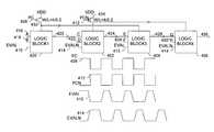
- FIG. 4illustrates how four smaller pre-charge PFETs may be replaced with two larger pre-charge PFETs, 432 and 434 .
- the subtreshhold leakagemay be reduced. Reducing the subtreshhold leakage reduces the power consumed by the logic shown in this example.
- FIG. 4contains a dynamic logic block chain and the signals that drive them.
- Logic Block 1 , 400is pre-charged through PFET, 432 , when voltage waveform, PC, 408 , goes low.
- PFET, 432W/L ratio is 4/0.2.
- Signals A, 416 , and B, 418are used to determine whether a pre-charge node stays high or goes low when the voltage waveform, EVAL, 410 , goes high.
- the output, 420 , of Logic Block 1 , 400drives input C of Logic Block 2 .
- Logic Block 2 , 402is pre-charged through PFET, 434 , when voltage waveform, PCN, 412 , goes low.
- PFET, 434 , W/L ratiois 4/0.2.
- Signals C, 420 , and D, 422are used to determine whether a pre-charge node stays high or goes low when the voltage waveform, EVALN, 414 , goes high.
- the output, 424 , of Logic Block 2 , 402drives input E of Logic Block 3 .
- Logic Block 3 , 404is pre-charged through PFET, 432 , when voltage waveform, PC, 408 , goes low.
- PFET, 432 , W/L ratiois 4/0.2.
- Signals E, 424 , and F, 426are used to determine whether a pre-charge node stays high or goes low when the voltage waveform, EVAL, 410 , goes high.
- the output, 428 , of Logic Block 3 , 404drives input G of Logic Block 4 .
- Logic Block 4 , 406is pre-charged through PFET, 434 , when voltage waveform, PCN, 412 , goes low.
- PFET, 434 , W/L ratiois 2/0.2.
- Signals G, 428 , and H, 430are used to determine whether a pre-charge node stays high or goes low when the voltage waveform, EVALN, 414 , goes high.
- the output, 436 , of Logic Block 4 , 406does not drive another dynamic logic block in this example.
Landscapes
- Engineering & Computer Science (AREA)
- Theoretical Computer Science (AREA)
- Physics & Mathematics (AREA)
- General Engineering & Computer Science (AREA)
- General Physics & Mathematics (AREA)
- Power Engineering (AREA)
- Computer Hardware Design (AREA)
- Computing Systems (AREA)
- Mathematical Physics (AREA)
- Logic Circuits (AREA)
Abstract
Description
Claims (9)
Priority Applications (2)
| Application Number | Priority Date | Filing Date | Title |
|---|---|---|---|
| US10/205,831US6624686B1 (en) | 2002-07-26 | 2002-07-26 | Method and apparatus for saving power in dynamic circuits |
| GB0316765AGB2391406B (en) | 2002-07-26 | 2003-07-17 | A method and apparatus for saving power in dynamic circuits |
Applications Claiming Priority (1)
| Application Number | Priority Date | Filing Date | Title |
|---|---|---|---|
| US10/205,831US6624686B1 (en) | 2002-07-26 | 2002-07-26 | Method and apparatus for saving power in dynamic circuits |
Publications (1)
| Publication Number | Publication Date |
|---|---|
| US6624686B1true US6624686B1 (en) | 2003-09-23 |
Family
ID=27765826
Family Applications (1)
| Application Number | Title | Priority Date | Filing Date |
|---|---|---|---|
| US10/205,831Expired - LifetimeUS6624686B1 (en) | 2002-07-26 | 2002-07-26 | Method and apparatus for saving power in dynamic circuits |
Country Status (2)
| Country | Link |
|---|---|
| US (1) | US6624686B1 (en) |
| GB (1) | GB2391406B (en) |
Cited By (2)
| Publication number | Priority date | Publication date | Assignee | Title |
|---|---|---|---|---|
| US20040041591A1 (en)* | 2002-08-27 | 2004-03-04 | Micron Technology, Inc. | Pseudo CMOS dynamic logic with delayed clocks |
| US20080211568A1 (en)* | 2007-03-01 | 2008-09-04 | Infineon Technologies Ag | MuGFET POWER SWITCH |
Citations (2)
| Publication number | Priority date | Publication date | Assignee | Title |
|---|---|---|---|---|
| US5825208A (en)* | 1996-05-20 | 1998-10-20 | International Business Machines Corporation | Method and apparatus for fast evaluation of dynamic CMOS logic circuits |
| US5872467A (en)* | 1997-07-31 | 1999-02-16 | Winbond Electronics Corporation | Dynamic comparator with improved pre-charge/set-up time |
Family Cites Families (2)
| Publication number | Priority date | Publication date | Assignee | Title |
|---|---|---|---|---|
| JP2679420B2 (en)* | 1991-02-01 | 1997-11-19 | 日本電気株式会社 | Semiconductor logic circuit |
| US5483181A (en)* | 1994-12-16 | 1996-01-09 | Sun Microsystems, Inc. | Dynamic logic circuit with reduced charge leakage |
- 2002
- 2002-07-26USUS10/205,831patent/US6624686B1/ennot_activeExpired - Lifetime
- 2003
- 2003-07-17GBGB0316765Apatent/GB2391406B/ennot_activeExpired - Fee Related
Patent Citations (2)
| Publication number | Priority date | Publication date | Assignee | Title |
|---|---|---|---|---|
| US5825208A (en)* | 1996-05-20 | 1998-10-20 | International Business Machines Corporation | Method and apparatus for fast evaluation of dynamic CMOS logic circuits |
| US5872467A (en)* | 1997-07-31 | 1999-02-16 | Winbond Electronics Corporation | Dynamic comparator with improved pre-charge/set-up time |
Cited By (7)
| Publication number | Priority date | Publication date | Assignee | Title |
|---|---|---|---|---|
| US20040041591A1 (en)* | 2002-08-27 | 2004-03-04 | Micron Technology, Inc. | Pseudo CMOS dynamic logic with delayed clocks |
| US20050024092A1 (en)* | 2002-08-27 | 2005-02-03 | Micron Technology, Inc. | Pseudo CMOS dynamic logic with delayed clocks |
| US6972599B2 (en) | 2002-08-27 | 2005-12-06 | Micron Technology Inc. | Pseudo CMOS dynamic logic with delayed clocks |
| US20050280445A1 (en)* | 2002-08-27 | 2005-12-22 | Micron Technology, Inc. | Pseudo CMOS dynamic logic with delayed clocks |
| US6980033B2 (en)* | 2002-08-27 | 2005-12-27 | Micron Technology, Inc. | Pseudo CMOS dynamic logic with delayed clocks |
| US7250789B2 (en)* | 2002-08-27 | 2007-07-31 | Micron Technology, Inc. | Pseudo-CMOS dynamic logic with delayed clocks |
| US20080211568A1 (en)* | 2007-03-01 | 2008-09-04 | Infineon Technologies Ag | MuGFET POWER SWITCH |
Also Published As
| Publication number | Publication date |
|---|---|
| GB2391406B (en) | 2006-03-22 |
| GB0316765D0 (en) | 2003-08-20 |
| GB2391406A (en) | 2004-02-04 |
Similar Documents
| Publication | Publication Date | Title |
|---|---|---|
| US6031778A (en) | Semiconductor integrated circuit | |
| US6268741B1 (en) | Semiconductor integrated circuits with power reduction mechanism | |
| US7639039B2 (en) | Semiconductor integrated circuit having current leakage reduction scheme | |
| US6297674B1 (en) | Semiconductor integrated circuit for low power and high speed operation | |
| EP0621694A2 (en) | Low power interface circuit | |
| US6864539B2 (en) | Semiconductor integrated circuit device having body biasing circuit for generating forward well bias voltage of suitable level by using simple circuitry | |
| US6952113B2 (en) | Method of reducing leakage current in sub one volt SOI circuits | |
| KR19990078417A (en) | Logic circuit having reduced power consumption | |
| US6759876B2 (en) | Semiconductor integrated circuit | |
| US20040105300A1 (en) | Reduced integrated circuit chip leakage and method of reducing leakage | |
| US20190123734A1 (en) | Apparatus with Electronic Circuitry Having Reduced Leakage Current and Associated Methods | |
| CN100592302C (en) | Integrated circuits including nested voltage islands | |
| CN1146638A (en) | Semiconductor device for reducing power dissipation in standby state | |
| Bhunia et al. | A novel synthesis approach for active leakage power reduction using dynamic supply gating | |
| US6624686B1 (en) | Method and apparatus for saving power in dynamic circuits | |
| US7805619B2 (en) | Circuit technique to reduce leakage during reduced power mode | |
| US20030197530A1 (en) | Semiconductor logical operation circuit | |
| JP3554638B2 (en) | Semiconductor circuit | |
| US6515935B1 (en) | Method and apparatus for reducing average power in memory arrays by switching a diode in or out of the ground path | |
| US5917367A (en) | Power supply solution for mixed signal circuits | |
| US20060077002A1 (en) | Apparatus and methods for saving power and reducing noise in integrated circuits | |
| US20070152745A1 (en) | System and method for reducing leakage current of an integrated circuit | |
| US20120120702A1 (en) | Power saving technique in a content addressable memory during compare operations | |
| US7855932B2 (en) | Low power word line control circuits with boosted voltage output for semiconductor memory | |
| JP4657421B2 (en) | Low power charge transfer method in an I/O system of an integrated circuit and low power I/O system |
Legal Events
| Date | Code | Title | Description |
|---|---|---|---|
| AS | Assignment | Owner name:HEWLETT-PACKARD COMPANY, COLORADO Free format text:ASSIGNMENT OF ASSIGNORS INTEREST;ASSIGNORS:GEDAMU, ELIAS;MAN, DENISE;MARSHALL, DAVID JOHN;REEL/FRAME:013561/0786 Effective date:20020725 | |
| AS | Assignment | Owner name:HEWLETT-PACKARD DEVELOPMENT COMPANY, L.P., COLORADO Free format text:ASSIGNMENT OF ASSIGNORS INTEREST;ASSIGNOR:HEWLETT-PACKARD COMPANY;REEL/FRAME:013776/0928 Effective date:20030131 Owner name:HEWLETT-PACKARD DEVELOPMENT COMPANY, L.P., COLORAD Free format text:ASSIGNMENT OF ASSIGNORS INTEREST;ASSIGNOR:HEWLETT-PACKARD COMPANY;REEL/FRAME:013776/0928 Effective date:20030131 Owner name:HEWLETT-PACKARD DEVELOPMENT COMPANY, L.P.,COLORADO Free format text:ASSIGNMENT OF ASSIGNORS INTEREST;ASSIGNOR:HEWLETT-PACKARD COMPANY;REEL/FRAME:013776/0928 Effective date:20030131 | |
| AS | Assignment | Owner name:HEWLETT-PACKARD DEVELOPMENT COMPANY, L.P., TEXAS Free format text:ASSIGNMENT OF ASSIGNORS INTEREST;ASSIGNOR:HEWLETT-PACKARD COMPANY;REEL/FRAME:013780/0741 Effective date:20030703 | |
| STCF | Information on status: patent grant | Free format text:PATENTED CASE | |
| FPAY | Fee payment | Year of fee payment:4 | |
| FPAY | Fee payment | Year of fee payment:8 | |
| AS | Assignment | Owner name:CONVERSANT INTELLECTUAL PROPERTY MANAGEMENT INC., Free format text:ASSIGNMENT OF ASSIGNORS INTEREST;ASSIGNOR:HEWLETT-PACKARD DEVELOPMENT COMPANY, L.P.;REEL/FRAME:034591/0627 Effective date:20141103 | |
| FPAY | Fee payment | Year of fee payment:12 | |
| AS | Assignment | Owner name:CPPIB CREDIT INVESTMENTS, INC., CANADA Free format text:AMENDED AND RESTATED U.S. PATENT SECURITY AGREEMENT (FOR NON-U.S. GRANTORS);ASSIGNOR:CONVERSANT INTELLECTUAL PROPERTY MANAGEMENT INC.;REEL/FRAME:046900/0136 Effective date:20180731 | |
| AS | Assignment | Owner name:CONVERSANT INTELLECTUAL PROPERTY MANAGEMENT INC., CANADA Free format text:RELEASE BY SECURED PARTY;ASSIGNOR:CPPIB CREDIT INVESTMENTS INC.;REEL/FRAME:054385/0435 Effective date:20201028 | |
| AS | Assignment | Owner name:MOSAID TECHNOLOGIES INCORPORATED, CANADA Free format text:CHANGE OF NAME;ASSIGNOR:CONVERSANT INTELLECTUAL PROPERTY INC.;REEL/FRAME:058796/0422 Effective date:20210401 | |
| AS | Assignment | Owner name:MOSAID TECHNOLOGIES INCORPORATED, CANADA Free format text:CORRECTIVE ASSIGNMENT TO CORRECT THE CONVEYING PARTY'S NAME PREVIOUSLY RECORDED ON REEL 058796 FRAME 0422. ASSIGNOR(S) HEREBY CONFIRMS THE CHANGE OF NAME;ASSIGNOR:CONVERSANT INTELLECTUAL PROPERTY MANAGEMENT INC.;REEL/FRAME:064707/0053 Effective date:20210401 |