US6624653B1 - Method and system for wafer level testing and burning-in semiconductor components - Google Patents
Method and system for wafer level testing and burning-in semiconductor componentsDownload PDFInfo
- Publication number
- US6624653B1 US6624653B1US10/037,562US3756202AUS6624653B1US 6624653 B1US6624653 B1US 6624653B1US 3756202 AUS3756202 AUS 3756202AUS 6624653 B1US6624653 B1US 6624653B1
- Authority
- US
- United States
- Prior art keywords
- contact structures
- components
- test
- testing
- resilient contact
- Prior art date
- Legal status (The legal status is an assumption and is not a legal conclusion. Google has not performed a legal analysis and makes no representation as to the accuracy of the status listed.)
- Expired - Lifetime
Links
- 238000012360testing methodMethods0.000titleclaimsabstractdescription137
- 239000004065semiconductorSubstances0.000titleclaimsabstractdescription48
- 238000000034methodMethods0.000titleclaimsabstractdescription45
- 239000000758substrateSubstances0.000claimsabstractdescription30
- 230000002950deficientEffects0.000claimsabstractdescription20
- 238000004891communicationMethods0.000claimsabstractdescription14
- 230000014759maintenance of locationEffects0.000claimsdescription24
- 238000005452bendingMethods0.000claimsdescription3
- 229910052751metalInorganic materials0.000abstractdescription10
- 239000002184metalSubstances0.000abstractdescription10
- 235000012431wafersNutrition0.000description80
- 239000000523sampleSubstances0.000description13
- 238000010998test methodMethods0.000description7
- 241000238631HexapodaSpecies0.000description3
- 238000010586diagramMethods0.000description3
- 239000011521glassSubstances0.000description3
- 230000013011matingEffects0.000description3
- 239000004697PolyetherimideSubstances0.000description2
- 239000000969carrierSubstances0.000description2
- 230000006835compressionEffects0.000description2
- 238000007906compressionMethods0.000description2
- 239000004020conductorSubstances0.000description2
- 238000007373indentationMethods0.000description2
- 238000002955isolationMethods0.000description2
- 238000004519manufacturing processMethods0.000description2
- 150000002739metalsChemical group0.000description2
- 229920003023plasticPolymers0.000description2
- 239000004033plasticSubstances0.000description2
- 229920001601polyetherimidePolymers0.000description2
- 239000011347resinSubstances0.000description2
- 229920005989resinPolymers0.000description2
- 238000007493shaping processMethods0.000description2
- JBRZTFJDHDCESZ-UHFFFAOYSA-NAsGaChemical compound[As]#[Ga]JBRZTFJDHDCESZ-UHFFFAOYSA-N0.000description1
- RYGMFSIKBFXOCR-UHFFFAOYSA-NCopperChemical compound[Cu]RYGMFSIKBFXOCR-UHFFFAOYSA-N0.000description1
- -1FR-4Polymers0.000description1
- 229910001218Gallium arsenideInorganic materials0.000description1
- UCKMPCXJQFINFW-UHFFFAOYSA-NSulphideChemical compound[S-2]UCKMPCXJQFINFW-UHFFFAOYSA-N0.000description1
- 230000002411adverseEffects0.000description1
- 229910052782aluminiumInorganic materials0.000description1
- XAGFODPZIPBFFR-UHFFFAOYSA-NaluminiumChemical compound[Al]XAGFODPZIPBFFR-UHFFFAOYSA-N0.000description1
- 230000015572biosynthetic processEffects0.000description1
- 239000000919ceramicSubstances0.000description1
- 229920001940conductive polymerPolymers0.000description1
- 229910052802copperInorganic materials0.000description1
- 239000010949copperSubstances0.000description1
- 230000001351cycling effectEffects0.000description1
- 238000013500data storageMethods0.000description1
- 230000008021depositionEffects0.000description1
- 239000012777electrically insulating materialSubstances0.000description1
- 238000005530etchingMethods0.000description1
- 229910052732germaniumInorganic materials0.000description1
- GNPVGFCGXDBREM-UHFFFAOYSA-Ngermanium atomChemical compound[Ge]GNPVGFCGXDBREM-UHFFFAOYSA-N0.000description1
- 238000010438heat treatmentMethods0.000description1
- 230000010354integrationEffects0.000description1
- 238000013507mappingMethods0.000description1
- 230000000873masking effectEffects0.000description1
- 239000000463materialSubstances0.000description1
- 238000012986modificationMethods0.000description1
- 230000004048modificationEffects0.000description1
- 229910021421monocrystalline siliconInorganic materials0.000description1
- 230000002093peripheral effectEffects0.000description1
- 150000003071polychlorinated biphenylsChemical class0.000description1
- 229920000642polymerPolymers0.000description1
- 229920006389polyphenyl polymerPolymers0.000description1
- 229920001296polysiloxanePolymers0.000description1
- 238000011160researchMethods0.000description1
- 230000000717retained effectEffects0.000description1
- 229910052594sapphireInorganic materials0.000description1
- 239000010980sapphireSubstances0.000description1
Images


Classifications
- G—PHYSICS
- G01—MEASURING; TESTING
- G01R—MEASURING ELECTRIC VARIABLES; MEASURING MAGNETIC VARIABLES
- G01R1/00—Details of instruments or arrangements of the types included in groups G01R5/00 - G01R13/00 and G01R31/00
- G01R1/02—General constructional details
- G01R1/04—Housings; Supporting members; Arrangements of terminals
- G01R1/0408—Test fixtures or contact fields; Connectors or connecting adaptors; Test clips; Test sockets
- G—PHYSICS
- G01—MEASURING; TESTING
- G01R—MEASURING ELECTRIC VARIABLES; MEASURING MAGNETIC VARIABLES
- G01R31/00—Arrangements for testing electric properties; Arrangements for locating electric faults; Arrangements for electrical testing characterised by what is being tested not provided for elsewhere
- G01R31/28—Testing of electronic circuits, e.g. by signal tracer
- G01R31/282—Testing of electronic circuits specially adapted for particular applications not provided for elsewhere
- G01R31/2831—Testing of materials or semi-finished products, e.g. semiconductor wafers or substrates
Definitions
- This inventionrelates generally to the testing of semiconductor components, and more particularly to the testing and burning-in of semiconductor components contained on a substrate, such as a semiconductor wafer.
- Semiconductor componentssuch as semiconductor dice and packages are routinely tested during manufacture.
- Semiconductor dicefor example, are typically fabricated on a semiconductor wafer using well known processes such as doping, masking, etching, and deposition of metals.
- the waferis probed and mapped to test the gross functionality of each die.
- a wafer prober and probe cardcan be used to electrically engage bond pads, or other test pads on the dice, and to apply test signals to the integrated circuits contained on the dice.
- the non functional diceare mapped in software or mechanically marked.
- the functional dicecan be singulated and packaged, or alternately retained in unpackaged form as known good die (KGD).
- Packaged diceare then burn-in tested by heating the dice while electrically biasing the integrated circuits on the dice.
- Bare dicecan be burn-in tested using temporary carriers configured to temporarily package the dice.
- Burn-in boardsare adapted to hold a large number of semiconductor packages, or temporary carriers for bare dice, in a chamber with temperature cycling capability. The burn-in boards are also in electrical communication with test circuitry configured to generate and to apply test signals to the dice.
- full functionality testcan be performed on the packaged or bare dice to evaluate various electrical characteristics of the integrated circuits.
- parameters that can be testedare input and output voltages, capacitance, pad leakage and current specifications.
- Memory devicescan also be subjected to logic tests wherein data storage, retrieval capabilities, and response times are measured.
- FIG. 1illustrates the prior art process sequence of fabricating the dice on the wafer, probe testing to identify functional dice, attaching resilient contact structures to the functional dice, and then burn-in testing the functional dice on the wafer using the resilient contact structures.
- FIG. 2Aillustrates a prior art semiconductor wafer 10 which comprises a plurality of semiconductor dice 12 having resilient contact structures 14 attached to bond pads 16 (FIG. 2C) of the dice 12 .
- the resilient contact structures 14have been attached to the functional dice 12 F on the wafer 10 responsive to wafer probe testing.
- each functional die 12 Fincludes the resilient contact structures 14
- each non-functional (defective) die 12 NFdoes not include the resilient contact structures 14 .
- FIG. 2Cillustrates the resilient contact structures 14 attached to the bond pads 16 on a functional die 12 F.
- the resilient contact structures 14include a core 18 which comprises a relatively low yield strength metal, and a shell 20 which comprises a relatively high yield strength metal. Both the core 18 and the shell 20 are formed with a resilient spring shape or spring segment.
- FIGS. 3A-3Fillustrate various prior art configurations for the resilient contact structures 14 .
- a resilient contact structure 14 Acomprises a cantilever beam oriented at an angle to a contact force F.
- the contact force Fcan be applied during formation of a pressure or bonded contact with a mating electronic component, such as a printed circuit board (PCB).
- a resilient contact structure 14 Bincludes an S-shape spring segment configured for contact by the contact force F or a contact force F′.
- a resilient contact structure 14 Cincludes a U-shape spring segment configured for contact by the contact force F.
- a resilient contact structure 14 Dincludes a curved spring segment configured for contact by the contact force F.
- a resilient contact structure 14 Eincludes a C-shaped spring segment configured for contact by the contact force F.
- a resilient contact structure 14 Fincludes a spring segment configured for contact by the contact force F.
- the wafer 10must first be probe tested, and the resilient contact structures 14 attached to only the functional dice 12 F.
- the non-functional dice 12 NFdo not include the resilient contact structures 14 because their electrical connection to the burn-in board may compromise the burn-in test procedure.
- conventional burn-in boardsinclude a power grid for establishing temporary electrical connections to multiple dice at one time. The burn-in boards thus utilize “shared resources” to test a large number of dice at the same time. Non-functional dice 12 NF can short the test signals, or otherwise adversely affect the test procedure.
- a test method, and a test system, for testing and burning-in semiconductor components on a substrateare provided.
- the substratecomprises a semiconductor wafer, and the components comprise semiconductor dice fabricated on the wafer.
- the test methodincludes the initial step of providing resilient contact structures on every component constructed as previously described.
- the test methodalso includes the step of testing the components to identify functional, and non functional (defective) components.
- the testing stepcan be performed using a wafer prober having a test board configured to electrically engage the resilient contact structures.
- the test methodalso includes the steps deforming the resilient contact structures on the non functional components to provide deformed contact structures, and then burn-in testing the functional components.
- the deformed contact structures on the non functional componentsprovide electrical isolation during burn-in testing, such that burn-in can be performed using a burn-in board and test circuitry that employ “shared resources”.
- Deformation of the resilient contact structurescan be performed using a deformation apparatus constructed in accordance with the invention.
- the deformation apparatusincludes a deformation block having a plurality of retention structures for physically engaging the resilient contact structures on the non functional components, and a substrate holder for holding the substrate proximate to the deformation block.
- Either the deformation block or the substrate holder (or both)can be configured for movement in X, Y and Z directions such that the resilient contact structures on the non functional components can be deformed by compression, bending or shaping. Movement of the deformation block, or the substrate holder (or both) can be accomplished using a wafer prober, an aligner bonder, a hexapod, or any tool that allows precision movement and placement of semiconductor components. With a wafer prober, the deformation block can be configured for positioning at the non-functional components responsive to wafer mapping software.
- the test systemincludes the deformation apparatus for deforming the resilient contact structures on the non functional components responsive to probe testing of the substrate.
- the test systemalso includes the substrate with the resilient contact structures on each functional component, and the deformed contact structures on each non functional component.
- the test systemalso includes a burn-in board, and a burn-in oven configured to burn-in test multiple substrates at the same time.
- the test systemincludes a test board having test pads configured to electrically engage the resilient contact structures on the functional components while maintaining a space between the deformed contact structures on the non functional components.
- the test pads on the test boardare in electrical communication with test circuitry, and are biased into electrical engagement with the resilient contact structures using a pressure plate and a spring member.
- An alternate embodiment test systemincludes a deformation block configured to electrically engage the resilient contact structures on each component, one component at a time, and to transmit test signals to the components to identify defective components.
- the deformation blockis configured to deform the resilient contact structures on the defective components to provide electrical isolation during a subsequent burn-in test.
- An alternate embodiment planarization systemincludes a deformation block configured to planarize the resilient contact structures on each component.
- the deformation blockcan be configured to just physically engage the resilient contact structures.
- the deformation blockcan be configured to physically and electrically engage the resilient contact structures, and to transmit test signal to the components.
- FIG. 1Ais a flow diagram illustrating process steps in a prior art wafer level burn-in process
- FIG. 2Ais a schematic plan view of a prior art semiconductor wafer having semiconductor dice and resilient contact structures for performing the wafer level burn-in process;
- FIG. 2Bis a schematic view taken along line 2 B of FIG. 2A illustrating the resilient contact structures on the wafer;
- FIG. 2Cis a cross sectional view taken along section line 2 C— 2 C of FIG. 2A illustrating the resilient contact structures
- FIGS. 3A-3Fare schematic cross sectional views illustrating various prior art resilient contact structures
- FIG. 4is a flow diagram illustrating process steps in a method for testing and burning-in semiconductor components in accordance with the invention
- FIGS. 5A-5Care schematic cross sectional views illustrating steps in the method, and components of a system constructed to perform the method;
- FIG. 6is a plan view taken along section line 6 — 6 of FIG. 5A illustrating a deformation block of a deformation apparatus constructed in accordance with the invention
- FIG. 6Ais a cross sectional view taken along section line 6 A— 6 A illustrating a retention structure on the deformation block;
- FIG. 6Bis a cross sectional view equivalent to FIG. 6A illustrating an alternate embodiment retention structure
- FIG. 6Cis a plan view taken along section line 6 C— 6 C of FIG. 6B of the alternate embodiment retention structure
- FIG. 6Dis a cross sectional view equivalent to FIG. 6A illustrating another alternate embodiment retention structure
- FIG. 6Eis a plan view taken along section line 6 E— 6 E of FIG. 6B of the alternate embodiment retention structure
- FIG. 6Fis a cross sectional view equivalent to FIG. 6A illustrating another alternate embodiment retention structure
- FIG. 7is a schematic plan view of a test system constructed in accordance with the invention.
- FIG. 7Ais a cross sectional view taken along section line 7 A— 7 A of FIG. 7 illustrating components of the test system
- FIG. 8is a schematic cross sectional view of an alternate embodiment test system constructed in accordance with the invention.
- FIG. 8Ais a cross sectional view taken along section line 8 A— 8 A of FIG. 8;
- FIGS. 9A-9Care schematic cross sectional views illustrating an alternate embodiment planarization system constructed in accordance with the invention.
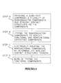
- FIG. 4a flow diagram illustrates steps in the method for testing and burning-in semiconductor components in accordance with the invention.
- Step AProviding a substrate comprising a plurality of semiconductor components and resilient contact structures on the components.
- semiconductor componentrefers to an electronic component that includes a semiconductor die.
- Exemplary semiconductor componentsinclude bare semiconductor dice, chip scale packages, ceramic or plastic semiconductor packages, BGA devices, and multi chip modules.
- the substratecomprises a semiconductor wafer and the semiconductor components comprise semiconductor dice contained on the wafer.
- Exemplary materials for the substrateinclude monocrystalline silicon, silicon-on-glass, silicon-on-sapphire, germanium and gallium arsenide.
- the substratecan comprise a glass filled resin, such as FR-4, or a plastic, such as polyetherimide (PEI) or polyphenyl sulfide (PPS).
- PEIpolyetherimide
- PPSpolyphenyl sulfide
- contact structuresrefers to terminal contacts in electrical communication with the integrated circuits contained on the semiconductor components.
- the term “resilient”refers to any shape that exhibits elastic movement responsive to a force applied to the contact structure. Exemplary “resilient contact structures” are illustrated in FIGS. 2 C and 3 A- 3 F. Resilient contact structures are further described in the previously cited Eldridge et al. patents, and in U.S. Pat. No. 5,495,667 to Farnworth et al.
- Step BTesting the semiconductor components to identify functional, and non functional (defective) components.
- This testing stepcan be performed using a conventional wafer prober for handling and electrically engaging the components on the substrate, and a tester for generating and applying test signals to the integrated circuits contained on the components.
- Suitable wafer probersare commercially available from Electroglass, as well as other manufacturers. Suitable testers are commercially available from Teradyne of Boston, Mass., as well as other manufacturers.
- the wafer probercan include a test board with contact pads, rather than a conventional probe card with probe needles, to make temporary electrical connections with the resilient contact structures. Such a test board will be more fully hereinafter described.
- Step CElectrically isolating the non functional components by deforming the resilient contact structures thereon.
- a deformation apparatus for deforming the resilient contact structurewill be more fully hereinafter described.
- Step DBurn-in testing the functional components.
- the deformed contact structure on the non functional componentsprovide electrical isolation, such that test signals are applied to only the functional components.
- a semiconductor wafer 10is provided.
- the wafer 10includes a plurality of semiconductor dice 12 containing integrated circuits and various semiconductor devices.
- Each die 12includes one or more patterns of resilient contact structures 14 in electrical communication with the integrated circuits and semiconductor devices contained on the die 12 .
- the resilient contact structures 14can be constructed substantially as previously described and shown in FIGS. 2 C and 3 A- 3 F.
- the dice 12have been tested to identify functional dice 12 F and non-functional dice 12 NF.
- a deformation apparatus 22is provided.
- the deformation apparatus 22is configured to deform one or more resilient contact structures 14 on the non-functional dice 12 NF one die at a time, such that a subsequent burn-in test can be performed without electrically contacting the non-functional dice 12 NF.
- the deformation apparatus 22can be configured to deform all of the resilient contact structures 14 on each non-functional die 12 NF.
- the deformation apparatus 22can be configured to deform selected resilient contact structures 14 , such as power or ground connections on each non-functional die 12 NF, leaving the remaining resilient contact structures 14 , such as address/control/data connections, intact.
- the deformation apparatus 22includes a die-sized deformation block 25 configured to physically contact and deform one or more of the resilient contact structures 14 on the non-functional dice 12 NF.
- the deformation apparatus 22also includes a block holder 26 configured to hold the deformation block 25 , and a wafer holder 28 configured to hold the wafer 10 during deformation of the resilient contact structures 14 by the deformation block 25 .
- the deformation block 25includes a plurality of retention structures 24 A formed thereon.
- the retention structures 24 Aare formed in a pattern that exactly matches a pattern of the resilient contact structures 14 on an individual die 12 . If only selected resilient contacts structures 14 on a die 12 are to be deformed, the retention structures 24 A align with selected resilient contact structures 14 on the die 12 (e.g., power pins, ground pins).
- the retention structures 24 Acomprise generally conical, v-shaped pockets or indentations, configured to retain and deform the resilient contact structures 14 on a single non-functional die 12 NF.
- the retention structures 24 Aare sized and shaped to facilitate compression, bending and shaping of the resilient contacts structures 14 .
- retention structures 24 Bcomprise pockets, or indentations in the deformation apparatus 22 , having a generally square or rectangular peripheral configuration.
- retention structures 24 Ccomprise elongated grooves configured to retain multiple resilient contact structures 14 at the same time.
- retention structures 24 Dcomprise a grooved, or rough surface on the deformation block 25 .
- the block holder 26 and the wafer holder 28are configured for X, Y and Z direction movement relative to one another, such that the retention structures 24 on the deformation block 25 can physically engage and deform the resilient contact structures 14 on the non-functional dice 12 NF.
- either the block holder 26 or the wafer holder 28 (or both)can be configured for movement in X, Y and Z directions.
- the block holder 26 and the wafer holder 28can be mounted to any precision tool that permits accurate alignment of the retention structures 24 on the deformation block 25 with the resilient contact structures 14 on the non functional dice 12 NF.
- the toolmust be able to move either the block holder 26 , or the wafer holder 28 (or both) in the Z direction to bring the deformation block 25 in physical contact with the resilient contact structures 14 on the non functional dice 12 NF.
- the toolmust be able to move either the block holder 26 or the wafer holder 28 (or both) in X or Y directions such that the deformation block 25 can bend, compress, shape or otherwise deform the resilient contact structures 14 .
- the block holder 26 and the wafer holder 28can be mounted to an automated wafer testing apparatus such as wafer prober.
- a conventional wafer probercan be modified to include the block holder 26 and the deformation block 25 in place of a conventional probe card fixture and probe card.
- movement of the wafer holder 28 or the block holder 26can be controlled by a controller 30 as in a conventional wafer prober.
- the controller 30can be programmed to use mapping information from the previous wafer level testing step, to locate the deformation block 25 at the non-functional dice 12 NF.
- the block holder 26 and the wafer holder 28can be mounted to a manual tool such as an aligner bonder tool.
- Aligner bonder toolsare commercially available from Research Devices of Piscataway, N.J., as well as other manufacturers.
- One suitable aligner bonder toolis described in U.S. Pat. No. 4,899,921 to Bendat et al. In this case viewing devices on the tool, rather than the controller 30 , can be used to locate the deformation block 25 at the non functional die 12 NF.
- the block holder 26 and the wafer holder 28can be mounted to a hexapod apparatus configured for moving either the deformation block 25 , or the wafer 10 in six degrees of freedom.
- a hexapod apparatusis described in U.S. Pat. No. 6,048,750 to Hembree.
- movement of the block holder 26 or the wafer holder 28 (or both) in the Z-directionbrings the deformation block 25 into physical contact with one or more of the resilient contact structures 14 on the non-functional dice 12 NF.
- movement of the block holder 26 or the wafer holder 28 (or both) in the X-direction or the Y-directioncompresses, bends, shapes, or otherwise deforms the resilient contact structures 14 on the non-functional dice 12 NF to form deformed contact structures 14 DE (FIG. 5 C).
- the retention structures 24 A on the deformation block 25help to retain the resilient contact structures 14 as they are being deformed.
- the retention structures 24 Acan be constructed to shape or re-shape the resilient contact structures 14 during the deformation step.
- the resilient contact structures 14are compressed, bent or shaped with a force that exceeds the yield strength of the metal, or metals, which form the resilient contact structures 14 .
- the deformation stepmust be performed to account for “spring back” of the deformed contact structures 14 DE.
- the deformed contact structures 14 DEremain after the deformation block 25 is withdrawn.
- the deformed contact structures 14 DEhave a first height H 1 , that is less than a second height H 2 of the remaining non-deformed resilient contact structures 14 .
- the height differentialcan be on the order of several microns to several mils or more. As will be further explained, this height differential can be used to prevent electrical contact with the non-functional dice 12 NF during a subsequent burn-in test.
- test system 31constructed in accordance with the invention is illustrated.
- the test system 31includes the previously described deformation apparatus 22 (FIG. 5 A).
- the test system 31includes a burn-in board 32 , a burn-in oven 34 configured for retention in the burn-in oven 34 , and test circuitry 36 in electrical communication with the burn-in board 32 .
- the burn-in board 32is configured to retain multiple wafers 10 in the burn-in oven 34 , while the test circuitry 36 electrically biases the integrated circuits contained on the dice 12 .
- the burn-in oven 34is configured to heat the wafers 10 to a temperature of at least 90° C., preferably between about 125° C. to 200° C., for between 8 to 168 hours, preferably between about 8 to 24 hours. Suitable burn-in ovens are manufactured by Micron Systems Integration under the trademark “AMBYX”.
- the test circuitry 36is configured to generate and apply test signals to the integrated circuits contained on the wafers 10 .
- the burn-in board 32includes an electrical connector 38 in electrical communication with the test circuitry 36 .
- the test system 31also includes a test board 40 for transmitting the test signals from the test circuitry 36 to the integrated circuits, and a pressure plate 46 for biasing test pads 42 on the test board 40 into physical and electrical contact with the resilient contact structures 14 on the wafer 10 .
- the test pads 42are in electrical communication with conductors 48 (FIG. 7) on the burn-in board 32 , which are in electrical communication with the electrical connector 38 and the test circuitry 36 .
- the test board 40can comprise a glass filled resin such as FR-4, and the test pads 42 can comprise a highly conductive metal, such as aluminum or copper.
- test board 40can include conductive traces and conductive vias (not shown), as is well known in the art, to establish electrical paths between the test pads 42 and the electrical connector 38 on the burn-in board 32 .
- the test board 40or one similar thereto, can be used to conduct the previous wafer probe test for identifying the functional dice 12 F and non-functional dice 12 NF.
- the test system 31also includes a spring member 44 , which comprises an elastomeric polymer, such as silicone, that cushions a force F applied by the pressure plate 46 to the test board 40 .
- the force Fcan be applied by any suitable mechanical element such as clips, fasteners, or weights.
- the burn-in board 32is constructed to prevent movement of the wafer 10 as the biasing force F is applied through the test board 40 to the resilient contact structures 14 .
- the test pads 42 on the test board 40are configured to contact all of the resilient contact structures 14 on the wafer 10 at the same time.
- the deformed contact structures 14 DE on the non-functional dice 12 NFare shorter than the resilient contact structures 14 on the functional dice 12 F. Accordingly, a space S is present between the deformed contact structures 14 DE and the mating test pads 42 on the test board 40 .
- the space Scan be from microns to several mils or greater, and prevents electrical communication between the test circuitry 36 and the non-functional dice 12 NF. This permits the test circuitry 36 to utilize “shared resources” to apply test signals to all of the functional dice 12 F at the same time.
- the test system 31 Aincludes a deformation block 25 A, a block holder 26 A for holding the deformation block 25 A, and a wafer holder 28 A for holding the wafer 10 .
- the deformation block 25 Ais configured to electrically engage the resilient contact structures 14 on each die 12 , one die at a time, and to apply test signals to the integrated circuits contained on the dice 12 .
- the deformation block 25 Ais configured to deform one or more of the resilient contact structures 14 on defective dice 12 NF identified by the test signals.
- the deformed contact structures 14(FIG. 7A) electrically isolate the defective dice 12 NF (FIG. 7A) on the wafer 10 during a subsequent burn-in test as previously described.
- the test system 31 Aalso includes a wafer prober 58 configured to align and move the deformation block 25 A and the wafer 10 into physical contact.
- the wafer prober 58can comprise a conventional wafer probe, and the deformation block 25 A can take the place of the probe card.
- the wafer prober 58must also be configured to move the deformation block 25 A, or the wafer 10 , or both, to deform the resilient contact structures 14 as previously described.
- the deformation block 25 Aalso includes electrically conductive retention structures 24 E having contact structures 52 configured to electrically engage the resilient contact structures 14 on the wafer 10 .
- the electrically conductive retention structures 24 Ecomprise conically shaped pockets as previously described, and the contact structures 52 comprise conductive layers in the pockets and metal filled vias in the deformation block 25 A
- the deformation block 25 Acan comprise an electrically insulating material, such as ceramic or plastic, and the contact structures 52 can be etched vias filled with a conductive material, such as metal or a conductive polymer.
- a conductive materialsuch as metal or a conductive polymer.
- other arrangementsare possible for retaining and electrically engaging the resilient contact structures 14 .
- electrical paths 54 on the block holder 26 Asuch as metal filled vias or signal traces, establish electrical communication with the contact structures 52 .
- Additional electrical paths 56 on the wafer prober 58such as “POGO PINS” or flex circuit, establish electrical communication with the test circuitry 36 A.
- the deformation block 25 Aelectrically engages the resilient contact structures 14 on each die 12 , one die at a time. Test signals can then be applied to the integrated circuits and semiconductor devices on each die 12 . If a die 12 NF is determined to be defective, then the deformation block 25 A can be moved as previously described, to deform the resilient contact structures 14 , and electrically isolate the defective die 12 NF for a subsequent wafer level burn-in test.
- planarization system 31 Bconfigured to planarize the resilient contact structures 14 on each die 12 , or the entire wafer 10 .
- the planarization system 31 Bincludes a deformation block 25 B, and a block holder 26 B configured to move the deformation block 25 B in X, Y and Z directions.
- the deformation block 25 Bcan be stationary and a wafer holder (not shown) can be configured to move the wafer 10 in X, Y and Z directions.
- the resilient contact structures 14 on the wafer 10can have variations in height making the resilient contact structures 14 on some dice 12 non-planar relative to one another. Stated differently, the Z-axis locations of the tip portions 18 of the resilient contact structures 14 can vary on a die 12 .
- the deformation block 25 Bis configured to physically engage the resilient contact structures 14 on one or more dice 12 (preferably all of the dice 12 on the wafer 10 at the same time), and to planarize the resilient contact structures 12 relative to one another by appropriate X, Y or Z direction movement of the deformation block 25 B.
- planarized contact structures 14 P on each die 12have a same height HP, such that the tip portions 18 P thereof are located along a common plane P.
- the planarized contact structures 14 Pfacilitate electrical mounting of the dice 12 to mating substrates such as PCBs.
- the deformation block 25 Bcan also be configured to electrically engage and transmit test signal to the components substantially as previously described for deformation block 25 A.
- the inventionprovides a method and a system for wafer level testing and burning-in semiconductor components such as semiconductor dice contained on a wafer. Also provided are a method and a system for planarizing resilient contact structures on semiconductor components.
Landscapes
- Physics & Mathematics (AREA)
- General Physics & Mathematics (AREA)
- Testing Or Measuring Of Semiconductors Or The Like (AREA)
- Testing Of Individual Semiconductor Devices (AREA)
- Measuring Leads Or Probes (AREA)
Abstract
Description
Claims (24)
Priority Applications (3)
| Application Number | Priority Date | Filing Date | Title |
|---|---|---|---|
| US10/037,562US6624653B1 (en) | 2000-08-28 | 2002-01-07 | Method and system for wafer level testing and burning-in semiconductor components |
| US10/445,778US6825685B2 (en) | 2000-08-28 | 2003-05-27 | Method and system for wafer level testing and burning-in semiconductor components |
| US10/893,685US7093622B2 (en) | 2000-08-28 | 2004-07-16 | Apparatus for deforming resilient contact structures on semiconductor components |
Applications Claiming Priority (2)
| Application Number | Priority Date | Filing Date | Title |
|---|---|---|---|
| US09/650,342US6462575B1 (en) | 2000-08-28 | 2000-08-28 | Method and system for wafer level testing and burning-in semiconductor components |
| US10/037,562US6624653B1 (en) | 2000-08-28 | 2002-01-07 | Method and system for wafer level testing and burning-in semiconductor components |
Related Parent Applications (1)
| Application Number | Title | Priority Date | Filing Date |
|---|---|---|---|
| US09/650,342DivisionUS6462575B1 (en) | 2000-08-28 | 2000-08-28 | Method and system for wafer level testing and burning-in semiconductor components |
Related Child Applications (1)
| Application Number | Title | Priority Date | Filing Date |
|---|---|---|---|
| US10/445,778DivisionUS6825685B2 (en) | 2000-08-28 | 2003-05-27 | Method and system for wafer level testing and burning-in semiconductor components |
Publications (1)
| Publication Number | Publication Date |
|---|---|
| US6624653B1true US6624653B1 (en) | 2003-09-23 |
Family
ID=24608499
Family Applications (4)
| Application Number | Title | Priority Date | Filing Date |
|---|---|---|---|
| US09/650,342Expired - Fee RelatedUS6462575B1 (en) | 2000-08-28 | 2000-08-28 | Method and system for wafer level testing and burning-in semiconductor components |
| US10/037,562Expired - LifetimeUS6624653B1 (en) | 2000-08-28 | 2002-01-07 | Method and system for wafer level testing and burning-in semiconductor components |
| US10/445,778Expired - Fee RelatedUS6825685B2 (en) | 2000-08-28 | 2003-05-27 | Method and system for wafer level testing and burning-in semiconductor components |
| US10/893,685Expired - LifetimeUS7093622B2 (en) | 2000-08-28 | 2004-07-16 | Apparatus for deforming resilient contact structures on semiconductor components |
Family Applications Before (1)
| Application Number | Title | Priority Date | Filing Date |
|---|---|---|---|
| US09/650,342Expired - Fee RelatedUS6462575B1 (en) | 2000-08-28 | 2000-08-28 | Method and system for wafer level testing and burning-in semiconductor components |
Family Applications After (2)
| Application Number | Title | Priority Date | Filing Date |
|---|---|---|---|
| US10/445,778Expired - Fee RelatedUS6825685B2 (en) | 2000-08-28 | 2003-05-27 | Method and system for wafer level testing and burning-in semiconductor components |
| US10/893,685Expired - LifetimeUS7093622B2 (en) | 2000-08-28 | 2004-07-16 | Apparatus for deforming resilient contact structures on semiconductor components |
Country Status (1)
| Country | Link |
|---|---|
| US (4) | US6462575B1 (en) |
Cited By (89)
| Publication number | Priority date | Publication date | Assignee | Title |
|---|---|---|---|---|
| US20020152046A1 (en)* | 2001-04-13 | 2002-10-17 | Velichko Sergey A. | Concurrent control of semiconductor parametric testing |
| US20030028343A1 (en)* | 2001-05-23 | 2003-02-06 | Micron Technology, Inc. | Intelligent measurement modular semiconductor parametric test system |
| US20030212523A1 (en)* | 2002-04-25 | 2003-11-13 | Micron Technology, Inc. | Dynamically adaptable semiconductor parametric testing |
| US20040210413A1 (en)* | 2003-04-17 | 2004-10-21 | Micron Technology, Inc. | Dynamic creation and modification of wafer test maps during wafer testing |
| US20040222518A1 (en)* | 2003-02-25 | 2004-11-11 | Tessera, Inc. | Ball grid array with bumps |
| US20040266036A1 (en)* | 2000-08-28 | 2004-12-30 | Cram Daniel P. | Apparatus for deforming resilient contact structures on semiconductor components |
| US20050012221A1 (en)* | 2003-07-14 | 2005-01-20 | Kirby Kyle K. | Semiconductor interconnect having conductive spring contacts, method of fabrication, and test systems incorporating the interconnect |
| US20050116326A1 (en)* | 2003-10-06 | 2005-06-02 | Tessera, Inc. | Formation of circuitry with modification of feature height |
| US20050168231A1 (en)* | 2003-12-24 | 2005-08-04 | Young-Gon Kim | Methods and structures for electronic probing arrays |
| US20050173805A1 (en)* | 2003-12-30 | 2005-08-11 | Tessera, Inc. | Micro pin grid array with pin motion isolation |
| US20050181544A1 (en)* | 2003-12-30 | 2005-08-18 | Tessera, Inc. | Microelectronic packages and methods therefor |
| US20050181655A1 (en)* | 2003-12-30 | 2005-08-18 | Tessera, Inc. | Micro pin grid array with wiping action |
| US20050284658A1 (en)* | 2003-10-06 | 2005-12-29 | Tessera, Inc. | Components with posts and pads |
| US20060028226A1 (en)* | 2004-07-21 | 2006-02-09 | Kreager Douglas P | Methods and apparatus for testing circuit boards |
| US20060040488A1 (en)* | 1994-12-29 | 2006-02-23 | Tessera, Inc. | Method of electrically connecting a microelectronic component |
| US20060049498A1 (en)* | 1994-09-20 | 2006-03-09 | Tessera, Inc. | Methods of making microelectronic assemblies including compliant interfaces |
| US20060249857A1 (en)* | 2005-03-16 | 2006-11-09 | Tessera, Inc. | Microelectronic packages and methods therefor |
| US20060261476A1 (en)* | 1995-10-31 | 2006-11-23 | Tessera, Inc. | Microelectronic assemblies having compliant layers |
| US20070148819A1 (en)* | 2005-12-23 | 2007-06-28 | Tessera, Inc. | Microelectronic assemblies having very fine pitch stacking |
| US20070148822A1 (en)* | 2005-12-23 | 2007-06-28 | Tessera, Inc. | Microelectronic packages and methods therefor |
| US20070205496A1 (en)* | 2004-06-25 | 2007-09-06 | Tessera, Inc. | Microelectronic packages and methods therefor |
| US20080003402A1 (en)* | 2003-10-06 | 2008-01-03 | Tessera, Inc. | Fine pitch microcontacts and method for forming thereof |
| US20080024457A1 (en)* | 2004-08-24 | 2008-01-31 | Jens Fliegner | Operating Device for a Motor Vehicle |
| US20080090427A1 (en)* | 2006-10-12 | 2008-04-17 | Tessera, Inc. | Microelectronic component with foam-metal posts |
| US20080088033A1 (en)* | 2006-10-17 | 2008-04-17 | Tessera, Inc. | Microelectronic packages and methods therefor |
| US20080150121A1 (en)* | 2006-12-20 | 2008-06-26 | Tessera Technologies Hungary Kft. | Microelectronic assemblies having compliancy and methods therefor |
| US20080150101A1 (en)* | 2006-12-20 | 2008-06-26 | Tessera, Inc. | Microelectronic packages having improved input/output connections and methods therefor |
| US7545029B2 (en) | 2006-08-18 | 2009-06-09 | Tessera, Inc. | Stack microelectronic assemblies |
| US20100044860A1 (en)* | 2008-08-21 | 2010-02-25 | Tessera Interconnect Materials, Inc. | Microelectronic substrate or element having conductive pads and metal posts joined thereto using bond layer |
| US7999379B2 (en) | 2005-02-25 | 2011-08-16 | Tessera, Inc. | Microelectronic assemblies having compliancy |
| US8183129B2 (en) | 2005-09-07 | 2012-05-22 | Infineon Technologies Ag | Alignment marks for polarized light lithography and method for use thereof |
| US8330272B2 (en) | 2010-07-08 | 2012-12-11 | Tessera, Inc. | Microelectronic packages with dual or multiple-etched flip-chip connectors |
| US8404520B1 (en) | 2011-10-17 | 2013-03-26 | Invensas Corporation | Package-on-package assembly with wire bond vias |
| RU2484489C2 (en)* | 2010-04-05 | 2013-06-10 | Государственное образовательное учреждение высшего профессионального образования "Воронежский государственный технический университет" | Method for rejecting semiconductor products with reduced reliability level |
| US8482111B2 (en) | 2010-07-19 | 2013-07-09 | Tessera, Inc. | Stackable molded microelectronic packages |
| US8525314B2 (en) | 2004-11-03 | 2013-09-03 | Tessera, Inc. | Stacked packaging improvements |
| US8558386B2 (en) | 1995-10-31 | 2013-10-15 | Tessera, Inc. | Methods of making compliant semiconductor chip packages |
| US8580607B2 (en) | 2010-07-27 | 2013-11-12 | Tessera, Inc. | Microelectronic packages with nanoparticle joining |
| US8623706B2 (en) | 2010-11-15 | 2014-01-07 | Tessera, Inc. | Microelectronic package with terminals on dielectric mass |
| US8835228B2 (en) | 2012-05-22 | 2014-09-16 | Invensas Corporation | Substrate-less stackable package with wire-bond interconnect |
| US8853558B2 (en) | 2010-12-10 | 2014-10-07 | Tessera, Inc. | Interconnect structure |
| US8872318B2 (en) | 2011-08-24 | 2014-10-28 | Tessera, Inc. | Through interposer wire bond using low CTE interposer with coarse slot apertures |
| US8878353B2 (en) | 2012-12-20 | 2014-11-04 | Invensas Corporation | Structure for microelectronic packaging with bond elements to encapsulation surface |
| US8884448B2 (en) | 2007-09-28 | 2014-11-11 | Tessera, Inc. | Flip chip interconnection with double post |
| US8883563B1 (en) | 2013-07-15 | 2014-11-11 | Invensas Corporation | Fabrication of microelectronic assemblies having stack terminals coupled by connectors extending through encapsulation |
| US8975738B2 (en) | 2012-11-12 | 2015-03-10 | Invensas Corporation | Structure for microelectronic packaging with terminals on dielectric mass |
| US9023691B2 (en) | 2013-07-15 | 2015-05-05 | Invensas Corporation | Microelectronic assemblies with stack terminals coupled by connectors extending through encapsulation |
| US9034696B2 (en) | 2013-07-15 | 2015-05-19 | Invensas Corporation | Microelectronic assemblies having reinforcing collars on connectors extending through encapsulation |
| US9082753B2 (en) | 2013-11-12 | 2015-07-14 | Invensas Corporation | Severing bond wire by kinking and twisting |
| US9087815B2 (en) | 2013-11-12 | 2015-07-21 | Invensas Corporation | Off substrate kinking of bond wire |
| US9093435B2 (en) | 2011-05-03 | 2015-07-28 | Tessera, Inc. | Package-on-package assembly with wire bonds to encapsulation surface |
| US9137903B2 (en) | 2010-12-21 | 2015-09-15 | Tessera, Inc. | Semiconductor chip assembly and method for making same |
| US9159708B2 (en) | 2010-07-19 | 2015-10-13 | Tessera, Inc. | Stackable molded microelectronic packages with area array unit connectors |
| US9214454B2 (en) | 2014-03-31 | 2015-12-15 | Invensas Corporation | Batch process fabrication of package-on-package microelectronic assemblies |
| US9224717B2 (en) | 2011-05-03 | 2015-12-29 | Tessera, Inc. | Package-on-package assembly with wire bonds to encapsulation surface |
| US9324681B2 (en) | 2010-12-13 | 2016-04-26 | Tessera, Inc. | Pin attachment |
| US9349706B2 (en) | 2012-02-24 | 2016-05-24 | Invensas Corporation | Method for package-on-package assembly with wire bonds to encapsulation surface |
| US9391008B2 (en) | 2012-07-31 | 2016-07-12 | Invensas Corporation | Reconstituted wafer-level package DRAM |
| US9412714B2 (en) | 2014-05-30 | 2016-08-09 | Invensas Corporation | Wire bond support structure and microelectronic package including wire bonds therefrom |
| US9502390B2 (en) | 2012-08-03 | 2016-11-22 | Invensas Corporation | BVA interposer |
| US9583411B2 (en) | 2014-01-17 | 2017-02-28 | Invensas Corporation | Fine pitch BVA using reconstituted wafer with area array accessible for testing |
| US9601454B2 (en) | 2013-02-01 | 2017-03-21 | Invensas Corporation | Method of forming a component having wire bonds and a stiffening layer |
| US9633971B2 (en) | 2015-07-10 | 2017-04-25 | Invensas Corporation | Structures and methods for low temperature bonding using nanoparticles |
| US9646917B2 (en) | 2014-05-29 | 2017-05-09 | Invensas Corporation | Low CTE component with wire bond interconnects |
| US9659848B1 (en) | 2015-11-18 | 2017-05-23 | Invensas Corporation | Stiffened wires for offset BVA |
| US9685365B2 (en) | 2013-08-08 | 2017-06-20 | Invensas Corporation | Method of forming a wire bond having a free end |
| US9691679B2 (en) | 2012-02-24 | 2017-06-27 | Invensas Corporation | Method for package-on-package assembly with wire bonds to encapsulation surface |
| US9728527B2 (en) | 2013-11-22 | 2017-08-08 | Invensas Corporation | Multiple bond via arrays of different wire heights on a same substrate |
| US9735084B2 (en) | 2014-12-11 | 2017-08-15 | Invensas Corporation | Bond via array for thermal conductivity |
| US9761554B2 (en) | 2015-05-07 | 2017-09-12 | Invensas Corporation | Ball bonding metal wire bond wires to metal pads |
| US9812402B2 (en) | 2015-10-12 | 2017-11-07 | Invensas Corporation | Wire bond wires for interference shielding |
| US9842745B2 (en) | 2012-02-17 | 2017-12-12 | Invensas Corporation | Heat spreading substrate with embedded interconnects |
| US9852969B2 (en) | 2013-11-22 | 2017-12-26 | Invensas Corporation | Die stacks with one or more bond via arrays of wire bond wires and with one or more arrays of bump interconnects |
| US9888579B2 (en) | 2015-03-05 | 2018-02-06 | Invensas Corporation | Pressing of wire bond wire tips to provide bent-over tips |
| US9911718B2 (en) | 2015-11-17 | 2018-03-06 | Invensas Corporation | ‘RDL-First’ packaged microelectronic device for a package-on-package device |
| US9935075B2 (en) | 2016-07-29 | 2018-04-03 | Invensas Corporation | Wire bonding method and apparatus for electromagnetic interference shielding |
| US9984992B2 (en) | 2015-12-30 | 2018-05-29 | Invensas Corporation | Embedded wire bond wires for vertical integration with separate surface mount and wire bond mounting surfaces |
| US10008469B2 (en) | 2015-04-30 | 2018-06-26 | Invensas Corporation | Wafer-level packaging using wire bond wires in place of a redistribution layer |
| US10008477B2 (en) | 2013-09-16 | 2018-06-26 | Invensas Corporation | Microelectronic element with bond elements to encapsulation surface |
| US10026717B2 (en) | 2013-11-22 | 2018-07-17 | Invensas Corporation | Multiple bond via arrays of different wire heights on a same substrate |
| US10181457B2 (en) | 2015-10-26 | 2019-01-15 | Invensas Corporation | Microelectronic package for wafer-level chip scale packaging with fan-out |
| US10299368B2 (en) | 2016-12-21 | 2019-05-21 | Invensas Corporation | Surface integrated waveguides and circuit structures therefor |
| US10332854B2 (en) | 2015-10-23 | 2019-06-25 | Invensas Corporation | Anchoring structure of fine pitch bva |
| US10381326B2 (en) | 2014-05-28 | 2019-08-13 | Invensas Corporation | Structure and method for integrated circuits packaging with increased density |
| US10460958B2 (en) | 2013-08-07 | 2019-10-29 | Invensas Corporation | Method of manufacturing embedded packaging with preformed vias |
| US10490528B2 (en) | 2015-10-12 | 2019-11-26 | Invensas Corporation | Embedded wire bond wires |
| US10535626B2 (en) | 2015-07-10 | 2020-01-14 | Invensas Corporation | Structures and methods for low temperature bonding using nanoparticles |
| US11973056B2 (en) | 2016-10-27 | 2024-04-30 | Adeia Semiconductor Technologies Llc | Methods for low temperature bonding using nanoparticles |
| US12211809B2 (en) | 2020-12-30 | 2025-01-28 | Adeia Semiconductor Bonding Technologies Inc. | Structure with conductive feature and method of forming same |
Families Citing this family (19)
| Publication number | Priority date | Publication date | Assignee | Title |
|---|---|---|---|---|
| JPH11354561A (en)* | 1998-06-09 | 1999-12-24 | Advantest Corp | Bump and method for forming the same |
| JP2001085480A (en)* | 1999-09-10 | 2001-03-30 | Mitsubishi Electric Corp | Semiconductor device and method of manufacturing semiconductor integrated circuit device |
| ITMI20010567A1 (en)* | 2001-03-19 | 2002-09-19 | Technoprobe S R L | VERTICAL PROBE MEASUREMENT HEAD FOR ELECTRONIC DEVICES INTEGRATED ON A SEMICONDUCTOR |
| US6472239B2 (en)* | 2001-04-02 | 2002-10-29 | Micron Technology, Inc. | Method for fabricating semiconductor components |
| US6680213B2 (en) | 2001-04-02 | 2004-01-20 | Micron Technology, Inc. | Method and system for fabricating contacts on semiconductor components |
| JP3813079B2 (en)* | 2001-10-11 | 2006-08-23 | 沖電気工業株式会社 | Chip size package |
| US7026646B2 (en) | 2002-06-20 | 2006-04-11 | Micron Technology, Inc. | Isolation circuit |
| US6967348B2 (en)* | 2002-06-20 | 2005-11-22 | Micron Technology, Inc. | Signal sharing circuit with microelectric die isolation features |
| US6920689B2 (en)* | 2002-12-06 | 2005-07-26 | Formfactor, Inc. | Method for making a socket to perform testing on integrated circuits |
| US7282932B2 (en)* | 2004-03-02 | 2007-10-16 | Micron Technology, Inc. | Compliant contact pin assembly, card system and methods thereof |
| US7544522B2 (en)* | 2004-06-09 | 2009-06-09 | Renesas Technology Corp. | Fabrication method of semiconductor integrated circuit device |
| US7167010B2 (en)* | 2004-09-02 | 2007-01-23 | Micron Technology, Inc. | Pin-in elastomer electrical contactor and methods and processes for making and using the same |
| KR100674938B1 (en)* | 2005-01-12 | 2007-01-26 | 삼성전자주식회사 | Probe Card for Multichip Test |
| KR100652421B1 (en)* | 2005-08-09 | 2006-12-01 | 삼성전자주식회사 | Donut type parallel probe card and wafer inspection method using the same |
| US7541825B2 (en)* | 2006-09-28 | 2009-06-02 | Micron Technology, Inc. | Isolation circuit |
| CH698962B1 (en)* | 2008-06-10 | 2014-10-31 | Rolex Sa | Barrel spring and method for its shaping. |
| US8237462B2 (en)* | 2009-08-11 | 2012-08-07 | Taiwan Semiconductor Manufacturing Company, Ltd. | Method for wafer-level testing of integrated circuits |
| US20170023617A1 (en)* | 2015-06-10 | 2017-01-26 | Translarity, Inc. | Shaping of contact structures for semiconductor test, and associated systems and methods |
| TWI737765B (en)* | 2016-07-08 | 2021-09-01 | 美商川斯萊緹公司 | Stacked stud bump contacts for wafer test contactors, and associated methods |
Citations (26)
| Publication number | Priority date | Publication date | Assignee | Title |
|---|---|---|---|---|
| US4961053A (en) | 1985-07-24 | 1990-10-02 | Heinz Krug | Circuit arrangement for testing integrated circuit components |
| US5070297A (en)* | 1990-06-04 | 1991-12-03 | Texas Instruments Incorporated | Full wafer integrated circuit testing device |
| US5241266A (en) | 1992-04-10 | 1993-08-31 | Micron Technology, Inc. | Built-in test circuit connection for wafer level burnin and testing of individual dies |
| US5347159A (en) | 1990-09-24 | 1994-09-13 | Tessera, Inc. | Semiconductor chip assemblies with face-up mounting and rear-surface connection to substrate |
| US5397997A (en)* | 1991-08-23 | 1995-03-14 | Nchip, Inc. | Burn-in technologies for unpackaged integrated circuits |
| US5476211A (en) | 1993-11-16 | 1995-12-19 | Form Factor, Inc. | Method of manufacturing electrical contacts, using a sacrificial member |
| US5495667A (en) | 1994-11-07 | 1996-03-05 | Micron Technology, Inc. | Method for forming contact pins for semiconductor dice and interconnects |
| US5557573A (en)* | 1995-08-21 | 1996-09-17 | Sgs-Thomson Microelectronics, Inc. | Entire wafer stress test method for integrated memory devices and circuit therefor |
| US5682061A (en) | 1990-09-24 | 1997-10-28 | Tessera, Inc. | Component for connecting a semiconductor chip to a substrate |
| US5685885A (en) | 1990-09-24 | 1997-11-11 | Tessera, Inc. | Wafer-scale techniques for fabrication of semiconductor chip assemblies |
| US5701666A (en) | 1994-08-31 | 1997-12-30 | Motorola, Inc. | Method for manufacturing a stimulus wafer for use in a wafer-to-wafer testing system to test integrated circuits located on a product wafer |
| US5796264A (en) | 1991-06-04 | 1998-08-18 | Micron Technology, Inc. | Apparatus for manufacturing known good semiconductor dice |
| US5844419A (en) | 1996-05-14 | 1998-12-01 | Micron Technology, Inc. | Method for testing semiconductor packages using decoupling capacitors to reduce noise |
| US5898629A (en)* | 1996-06-13 | 1999-04-27 | Micron Technology, Inc. | System for stressing a memory integrated circuit die |
| US5917707A (en) | 1993-11-16 | 1999-06-29 | Formfactor, Inc. | Flexible contact structure with an electrically conductive shell |
| US5949242A (en) | 1991-06-04 | 1999-09-07 | Micron Technology, Inc. | Method and apparatus for testing unpackaged semiconductor dice |
| US5966022A (en) | 1996-11-08 | 1999-10-12 | W. L. Gore & Associates, Inc. | Wafer level burn-in system |
| US5974662A (en) | 1993-11-16 | 1999-11-02 | Formfactor, Inc. | Method of planarizing tips of probe elements of a probe card assembly |
| US6023103A (en) | 1994-11-15 | 2000-02-08 | Formfactor, Inc. | Chip-scale carrier for semiconductor devices including mounted spring contacts |
| US6032356A (en) | 1993-11-16 | 2000-03-07 | Formfactor. Inc. | Wafer-level test and burn-in, and semiconductor process |
| US6043563A (en) | 1997-05-06 | 2000-03-28 | Formfactor, Inc. | Electronic components with terminals and spring contact elements extending from areas which are remote from the terminals |
| US6046600A (en) | 1995-10-31 | 2000-04-04 | Texas Instruments Incorporated | Process of testing integrated circuit dies on a wafer |
| US6049215A (en) | 1992-11-20 | 2000-04-11 | Kulicke & Soffa Ind. Inc. | Bare die carrier |
| US6064213A (en) | 1993-11-16 | 2000-05-16 | Formfactor, Inc. | Wafer-level burn-in and test |
| US6351134B2 (en)* | 1995-08-09 | 2002-02-26 | International Business Machines Corporation | Semiconductor wafer test and burn-in |
| US6462575B1 (en) | 2000-08-28 | 2002-10-08 | Micron Technology, Inc. | Method and system for wafer level testing and burning-in semiconductor components |
Family Cites Families (12)
| Publication number | Priority date | Publication date | Assignee | Title |
|---|---|---|---|---|
| US3573617A (en)* | 1967-10-27 | 1971-04-06 | Aai Corp | Method and apparatus for testing packaged integrated circuits |
| US3520336A (en)* | 1968-08-26 | 1970-07-14 | Universal Instruments Corp | Straightener assembly including integrated pre-straightener for electronic component leads |
| GB1253725A (en)* | 1969-02-14 | 1971-11-17 | Standard Telephones Cables Ltd | Lead wire locating device |
| US3972356A (en)* | 1974-09-23 | 1976-08-03 | Torben Kjarsgaard | Lead straightening, aligning, and spacing implement for an electronic semi-conductor package |
| US4002191A (en)* | 1975-09-15 | 1977-01-11 | Gianni Lorenzini | Apparatus and method for straightening semi-conductor pins |
| US4510686A (en)* | 1983-04-11 | 1985-04-16 | Universal Instruments Corporation | Method and apparatus for straightening and aligning leads and testing electrical functioning of components |
| US4824632A (en)* | 1987-12-31 | 1989-04-25 | Westinghouse Electric Corp. | Fuel assembly alignment pin straightening device |
| US4950980A (en)* | 1988-07-29 | 1990-08-21 | Pfaff Wayne | Test socket for electronic device packages |
| US4899921A (en)* | 1988-10-28 | 1990-02-13 | The American Optical Corporation | Aligner bonder |
| US5170117A (en)* | 1992-03-26 | 1992-12-08 | Chio Chuy Nan | Socket for testing a plug-in type semiconductor |
| EP0777652B1 (en) | 1994-08-18 | 2003-06-25 | Pfizer Inc. | Neuroprotective 3-(piperidinyl-1)-chroman-4,7-diol and 1-(4-hydrophenyl)-2-(piperidinyl-1)-alkanol derivatives |
| US6048750A (en)* | 1997-11-24 | 2000-04-11 | Micron Technology, Inc. | Method for aligning and connecting semiconductor components to substrates |
- 2000
- 2000-08-28USUS09/650,342patent/US6462575B1/ennot_activeExpired - Fee Related
- 2002
- 2002-01-07USUS10/037,562patent/US6624653B1/ennot_activeExpired - Lifetime
- 2003
- 2003-05-27USUS10/445,778patent/US6825685B2/ennot_activeExpired - Fee Related
- 2004
- 2004-07-16USUS10/893,685patent/US7093622B2/ennot_activeExpired - Lifetime
Patent Citations (26)
| Publication number | Priority date | Publication date | Assignee | Title |
|---|---|---|---|---|
| US4961053A (en) | 1985-07-24 | 1990-10-02 | Heinz Krug | Circuit arrangement for testing integrated circuit components |
| US5070297A (en)* | 1990-06-04 | 1991-12-03 | Texas Instruments Incorporated | Full wafer integrated circuit testing device |
| US5682061A (en) | 1990-09-24 | 1997-10-28 | Tessera, Inc. | Component for connecting a semiconductor chip to a substrate |
| US5347159A (en) | 1990-09-24 | 1994-09-13 | Tessera, Inc. | Semiconductor chip assemblies with face-up mounting and rear-surface connection to substrate |
| US5685885A (en) | 1990-09-24 | 1997-11-11 | Tessera, Inc. | Wafer-scale techniques for fabrication of semiconductor chip assemblies |
| US5949242A (en) | 1991-06-04 | 1999-09-07 | Micron Technology, Inc. | Method and apparatus for testing unpackaged semiconductor dice |
| US5796264A (en) | 1991-06-04 | 1998-08-18 | Micron Technology, Inc. | Apparatus for manufacturing known good semiconductor dice |
| US5397997A (en)* | 1991-08-23 | 1995-03-14 | Nchip, Inc. | Burn-in technologies for unpackaged integrated circuits |
| US5241266A (en) | 1992-04-10 | 1993-08-31 | Micron Technology, Inc. | Built-in test circuit connection for wafer level burnin and testing of individual dies |
| US6049215A (en) | 1992-11-20 | 2000-04-11 | Kulicke & Soffa Ind. Inc. | Bare die carrier |
| US6064213A (en) | 1993-11-16 | 2000-05-16 | Formfactor, Inc. | Wafer-level burn-in and test |
| US5476211A (en) | 1993-11-16 | 1995-12-19 | Form Factor, Inc. | Method of manufacturing electrical contacts, using a sacrificial member |
| US6032356A (en) | 1993-11-16 | 2000-03-07 | Formfactor. Inc. | Wafer-level test and burn-in, and semiconductor process |
| US5917707A (en) | 1993-11-16 | 1999-06-29 | Formfactor, Inc. | Flexible contact structure with an electrically conductive shell |
| US5974662A (en) | 1993-11-16 | 1999-11-02 | Formfactor, Inc. | Method of planarizing tips of probe elements of a probe card assembly |
| US5701666A (en) | 1994-08-31 | 1997-12-30 | Motorola, Inc. | Method for manufacturing a stimulus wafer for use in a wafer-to-wafer testing system to test integrated circuits located on a product wafer |
| US5495667A (en) | 1994-11-07 | 1996-03-05 | Micron Technology, Inc. | Method for forming contact pins for semiconductor dice and interconnects |
| US6023103A (en) | 1994-11-15 | 2000-02-08 | Formfactor, Inc. | Chip-scale carrier for semiconductor devices including mounted spring contacts |
| US6351134B2 (en)* | 1995-08-09 | 2002-02-26 | International Business Machines Corporation | Semiconductor wafer test and burn-in |
| US5557573A (en)* | 1995-08-21 | 1996-09-17 | Sgs-Thomson Microelectronics, Inc. | Entire wafer stress test method for integrated memory devices and circuit therefor |
| US6046600A (en) | 1995-10-31 | 2000-04-04 | Texas Instruments Incorporated | Process of testing integrated circuit dies on a wafer |
| US5844419A (en) | 1996-05-14 | 1998-12-01 | Micron Technology, Inc. | Method for testing semiconductor packages using decoupling capacitors to reduce noise |
| US5898629A (en)* | 1996-06-13 | 1999-04-27 | Micron Technology, Inc. | System for stressing a memory integrated circuit die |
| US5966022A (en) | 1996-11-08 | 1999-10-12 | W. L. Gore & Associates, Inc. | Wafer level burn-in system |
| US6043563A (en) | 1997-05-06 | 2000-03-28 | Formfactor, Inc. | Electronic components with terminals and spring contact elements extending from areas which are remote from the terminals |
| US6462575B1 (en) | 2000-08-28 | 2002-10-08 | Micron Technology, Inc. | Method and system for wafer level testing and burning-in semiconductor components |
Cited By (215)
| Publication number | Priority date | Publication date | Assignee | Title |
|---|---|---|---|---|
| US20060049498A1 (en)* | 1994-09-20 | 2006-03-09 | Tessera, Inc. | Methods of making microelectronic assemblies including compliant interfaces |
| US7368818B2 (en) | 1994-09-20 | 2008-05-06 | Tessera, Inc. | Methods of making microelectronic assemblies including compliant interfaces |
| US20090200654A1 (en)* | 1994-12-29 | 2009-08-13 | Tessera, Inc. | Method of electrically connecting a microelectronic component |
| US20090200655A1 (en)* | 1994-12-29 | 2009-08-13 | Tessera, Inc. | Method of electrically connecting a microelectronic component |
| US7531894B2 (en) | 1994-12-29 | 2009-05-12 | Tessera, Inc. | Method of electrically connecting a microelectronic component |
| US8513799B2 (en) | 1994-12-29 | 2013-08-20 | Tessera, Inc. | Method of electrically connecting a microelectronic component |
| US8148199B2 (en) | 1994-12-29 | 2012-04-03 | Tessera, Inc. | Method of electrically connecting a microelectronic component |
| US20090236406A1 (en)* | 1994-12-29 | 2009-09-24 | Tessera, Inc. | Method of electrically connecting a microelectronic component |
| US7528008B2 (en) | 1994-12-29 | 2009-05-05 | Tessera, Inc. | Method of electrically connecting a microelectronic component |
| US20110017704A1 (en)* | 1994-12-29 | 2011-01-27 | Tessera, Inc. | Method of electrically connecting a microelectronic component |
| US8114711B2 (en) | 1994-12-29 | 2012-02-14 | Tessera, Inc. | Method of electrically connecting a microelectronic component |
| US8148205B2 (en) | 1994-12-29 | 2012-04-03 | Tessera, Inc. | Method of electrically connecting a microelectronic component |
| US20060040488A1 (en)* | 1994-12-29 | 2006-02-23 | Tessera, Inc. | Method of electrically connecting a microelectronic component |
| US20070066046A1 (en)* | 1994-12-29 | 2007-03-22 | Tessera, Inc. | Method of electrically connecting a microelectronic component |
| US20060261476A1 (en)* | 1995-10-31 | 2006-11-23 | Tessera, Inc. | Microelectronic assemblies having compliant layers |
| US8558386B2 (en) | 1995-10-31 | 2013-10-15 | Tessera, Inc. | Methods of making compliant semiconductor chip packages |
| US7408260B2 (en) | 1995-10-31 | 2008-08-05 | Tessera, Inc. | Microelectronic assemblies having compliant layers |
| US7093622B2 (en) | 2000-08-28 | 2006-08-22 | Micron Technology, Inc. | Apparatus for deforming resilient contact structures on semiconductor components |
| US20040266036A1 (en)* | 2000-08-28 | 2004-12-30 | Cram Daniel P. | Apparatus for deforming resilient contact structures on semiconductor components |
| US20020152046A1 (en)* | 2001-04-13 | 2002-10-17 | Velichko Sergey A. | Concurrent control of semiconductor parametric testing |
| US7337088B2 (en) | 2001-05-23 | 2008-02-26 | Micron Technology, Inc. | Intelligent measurement modular semiconductor parametric test system |
| US20030028343A1 (en)* | 2001-05-23 | 2003-02-06 | Micron Technology, Inc. | Intelligent measurement modular semiconductor parametric test system |
| US7162386B2 (en) | 2002-04-25 | 2007-01-09 | Micron Technology, Inc. | Dynamically adaptable semiconductor parametric testing |
| US20060122803A1 (en)* | 2002-04-25 | 2006-06-08 | Micron Technology, Inc. | Dynamically adaptable semiconductor parametric testing |
| US20060125509A1 (en)* | 2002-04-25 | 2006-06-15 | Micron Technology, Inc. | Dynamically adaptable semiconductor parametric testing |
| US20030212523A1 (en)* | 2002-04-25 | 2003-11-13 | Micron Technology, Inc. | Dynamically adaptable semiconductor parametric testing |
| US7383147B2 (en) | 2002-04-25 | 2008-06-03 | Micron Technology, Inc. | Dynamically adaptable semiconductor parametric testing |
| US20050021273A1 (en)* | 2002-04-25 | 2005-01-27 | Micron Technology, Inc. | Dynamically adaptable semiconductor parametric testing |
| US7165004B2 (en) | 2002-04-25 | 2007-01-16 | Micron Technology, Inc. | Dynamically adaptable semiconductor parametric testing |
| US7139672B2 (en) | 2002-04-25 | 2006-11-21 | Micron Technology, Inc. | Dynamically adaptable semiconductor parametric testing |
| US20040222518A1 (en)* | 2003-02-25 | 2004-11-11 | Tessera, Inc. | Ball grid array with bumps |
| US20040210413A1 (en)* | 2003-04-17 | 2004-10-21 | Micron Technology, Inc. | Dynamic creation and modification of wafer test maps during wafer testing |
| US7010451B2 (en) | 2003-04-17 | 2006-03-07 | Micron Technology, Inc. | Dynamic creation and modification of wafer test maps during wafer testing |
| US20060064268A1 (en)* | 2003-04-17 | 2006-03-23 | Micron Technology, Inc. | Dynamic creation and modification of wafer test maps during wafer testing |
| US20060125107A1 (en)* | 2003-07-14 | 2006-06-15 | Kirby Kyle K | Test system for semiconductor components having conductive spring contacts |
| US7411304B2 (en) | 2003-07-14 | 2008-08-12 | Micron Technology, Inc. | Semiconductor interconnect having conductive spring contacts |
| US20050146047A1 (en)* | 2003-07-14 | 2005-07-07 | Kirby Kyle K. | Method for fabricating a semiconductor interconnect having conductive spring contacts |
| US7042080B2 (en) | 2003-07-14 | 2006-05-09 | Micron Technology, Inc. | Semiconductor interconnect having compliant conductive contacts |
| US7314821B2 (en) | 2003-07-14 | 2008-01-01 | Micron Technology, Inc. | Method for fabricating a semiconductor interconnect having conductive spring contacts |
| US7449910B2 (en) | 2003-07-14 | 2008-11-11 | Micron Technology, Inc. | Test system for semiconductor components having conductive spring contacts |
| US20050116351A1 (en)* | 2003-07-14 | 2005-06-02 | Kirby Kyle K. | Semiconductor interconnect having conductive spring contacts |
| US7391117B2 (en) | 2003-07-14 | 2008-06-24 | Micron Technology, Inc. | Method for fabricating semiconductor components with conductive spring contacts |
| US20060145353A1 (en)* | 2003-07-14 | 2006-07-06 | Kirby Kyle K | Semiconductor interconnect having dome shaped conductive spring contacts |
| US20060125106A1 (en)* | 2003-07-14 | 2006-06-15 | Kirby Kyle K | Method for fabricating semiconductor components with conductive spring contacts |
| US20050012221A1 (en)* | 2003-07-14 | 2005-01-20 | Kirby Kyle K. | Semiconductor interconnect having conductive spring contacts, method of fabrication, and test systems incorporating the interconnect |
| US8046912B2 (en) | 2003-10-06 | 2011-11-01 | Tessera, Inc. | Method of making a connection component with posts and pads |
| US7816251B2 (en) | 2003-10-06 | 2010-10-19 | Tessera, Inc. | Formation of circuitry with modification of feature height |
| US20050116326A1 (en)* | 2003-10-06 | 2005-06-02 | Tessera, Inc. | Formation of circuitry with modification of feature height |
| US20080003402A1 (en)* | 2003-10-06 | 2008-01-03 | Tessera, Inc. | Fine pitch microcontacts and method for forming thereof |
| US20090133254A1 (en)* | 2003-10-06 | 2009-05-28 | Tessera, Inc. | Components with posts and pads |
| US20050284658A1 (en)* | 2003-10-06 | 2005-12-29 | Tessera, Inc. | Components with posts and pads |
| US8641913B2 (en) | 2003-10-06 | 2014-02-04 | Tessera, Inc. | Fine pitch microcontacts and method for forming thereof |
| US7462936B2 (en) | 2003-10-06 | 2008-12-09 | Tessera, Inc. | Formation of circuitry with modification of feature height |
| US7495179B2 (en) | 2003-10-06 | 2009-02-24 | Tessera, Inc. | Components with posts and pads |
| US8604348B2 (en) | 2003-10-06 | 2013-12-10 | Tessera, Inc. | Method of making a connection component with posts and pads |
| US20050168231A1 (en)* | 2003-12-24 | 2005-08-04 | Young-Gon Kim | Methods and structures for electronic probing arrays |
| US7709968B2 (en) | 2003-12-30 | 2010-05-04 | Tessera, Inc. | Micro pin grid array with pin motion isolation |
| US20050173805A1 (en)* | 2003-12-30 | 2005-08-11 | Tessera, Inc. | Micro pin grid array with pin motion isolation |
| US8207604B2 (en) | 2003-12-30 | 2012-06-26 | Tessera, Inc. | Microelectronic package comprising offset conductive posts on compliant layer |
| US8531039B2 (en) | 2003-12-30 | 2013-09-10 | Tessera, Inc. | Micro pin grid array with pin motion isolation |
| US7554206B2 (en) | 2003-12-30 | 2009-06-30 | Tessera, Inc. | Microelectronic packages and methods therefor |
| US20050181655A1 (en)* | 2003-12-30 | 2005-08-18 | Tessera, Inc. | Micro pin grid array with wiping action |
| US7176043B2 (en) | 2003-12-30 | 2007-02-13 | Tessera, Inc. | Microelectronic packages and methods therefor |
| US20050181544A1 (en)* | 2003-12-30 | 2005-08-18 | Tessera, Inc. | Microelectronic packages and methods therefor |
| US7999397B2 (en) | 2004-06-25 | 2011-08-16 | Tessera, Inc. | Microelectronic packages and methods therefor |
| US7745943B2 (en) | 2004-06-25 | 2010-06-29 | Tessera, Inc. | Microelectonic packages and methods therefor |
| US20070205496A1 (en)* | 2004-06-25 | 2007-09-06 | Tessera, Inc. | Microelectronic packages and methods therefor |
| US8329581B2 (en) | 2004-06-25 | 2012-12-11 | Tessera, Inc. | Microelectronic packages and methods therefor |
| US20060028226A1 (en)* | 2004-07-21 | 2006-02-09 | Kreager Douglas P | Methods and apparatus for testing circuit boards |
| US7339368B2 (en)* | 2004-07-21 | 2008-03-04 | Intel Corporation | Methods and apparatus for testing circuit boards |
| US9644984B2 (en)* | 2004-08-24 | 2017-05-09 | Volkswagen Ag | Operating device for a motor vehicle |
| US20080024457A1 (en)* | 2004-08-24 | 2008-01-31 | Jens Fliegner | Operating Device for a Motor Vehicle |
| US8927337B2 (en) | 2004-11-03 | 2015-01-06 | Tessera, Inc. | Stacked packaging improvements |
| US8525314B2 (en) | 2004-11-03 | 2013-09-03 | Tessera, Inc. | Stacked packaging improvements |
| US8531020B2 (en) | 2004-11-03 | 2013-09-10 | Tessera, Inc. | Stacked packaging improvements |
| US9570416B2 (en) | 2004-11-03 | 2017-02-14 | Tessera, Inc. | Stacked packaging improvements |
| US9153562B2 (en) | 2004-11-03 | 2015-10-06 | Tessera, Inc. | Stacked packaging improvements |
| US7999379B2 (en) | 2005-02-25 | 2011-08-16 | Tessera, Inc. | Microelectronic assemblies having compliancy |
| US7939934B2 (en) | 2005-03-16 | 2011-05-10 | Tessera, Inc. | Microelectronic packages and methods therefor |
| US20060249857A1 (en)* | 2005-03-16 | 2006-11-09 | Tessera, Inc. | Microelectronic packages and methods therefor |
| US8183129B2 (en) | 2005-09-07 | 2012-05-22 | Infineon Technologies Ag | Alignment marks for polarized light lithography and method for use thereof |
| US8067267B2 (en) | 2005-12-23 | 2011-11-29 | Tessera, Inc. | Microelectronic assemblies having very fine pitch stacking |
| US9218988B2 (en) | 2005-12-23 | 2015-12-22 | Tessera, Inc. | Microelectronic packages and methods therefor |
| US20070148819A1 (en)* | 2005-12-23 | 2007-06-28 | Tessera, Inc. | Microelectronic assemblies having very fine pitch stacking |
| US8058101B2 (en) | 2005-12-23 | 2011-11-15 | Tessera, Inc. | Microelectronic packages and methods therefor |
| US8728865B2 (en) | 2005-12-23 | 2014-05-20 | Tessera, Inc. | Microelectronic packages and methods therefor |
| US20100232129A1 (en)* | 2005-12-23 | 2010-09-16 | Tessera, Inc. | Microelectronic packages and methods therefor |
| US8093697B2 (en) | 2005-12-23 | 2012-01-10 | Tessera, Inc. | Microelectronic packages and methods therefor |
| US20070148822A1 (en)* | 2005-12-23 | 2007-06-28 | Tessera, Inc. | Microelectronic packages and methods therefor |
| US9984901B2 (en) | 2005-12-23 | 2018-05-29 | Tessera, Inc. | Method for making a microelectronic assembly having conductive elements |
| US7545029B2 (en) | 2006-08-18 | 2009-06-09 | Tessera, Inc. | Stack microelectronic assemblies |
| US7510401B2 (en) | 2006-10-12 | 2009-03-31 | Tessera, Inc. | Microelectronic component with foam-metal posts |
| US20080090427A1 (en)* | 2006-10-12 | 2008-04-17 | Tessera, Inc. | Microelectronic component with foam-metal posts |
| US20080088033A1 (en)* | 2006-10-17 | 2008-04-17 | Tessera, Inc. | Microelectronic packages and methods therefor |
| US7719121B2 (en) | 2006-10-17 | 2010-05-18 | Tessera, Inc. | Microelectronic packages and methods therefor |
| US20080150121A1 (en)* | 2006-12-20 | 2008-06-26 | Tessera Technologies Hungary Kft. | Microelectronic assemblies having compliancy and methods therefor |
| US7749886B2 (en) | 2006-12-20 | 2010-07-06 | Tessera, Inc. | Microelectronic assemblies having compliancy and methods therefor |
| US8115308B2 (en) | 2006-12-20 | 2012-02-14 | Tessera, Inc. | Microelectronic assemblies having compliancy and methods therefor |
| US20080150101A1 (en)* | 2006-12-20 | 2008-06-26 | Tessera, Inc. | Microelectronic packages having improved input/output connections and methods therefor |
| US8759973B2 (en) | 2006-12-20 | 2014-06-24 | Tessera, Inc. | Microelectronic assemblies having compliancy and methods therefor |
| US8884448B2 (en) | 2007-09-28 | 2014-11-11 | Tessera, Inc. | Flip chip interconnection with double post |
| US20100044860A1 (en)* | 2008-08-21 | 2010-02-25 | Tessera Interconnect Materials, Inc. | Microelectronic substrate or element having conductive pads and metal posts joined thereto using bond layer |
| RU2484489C2 (en)* | 2010-04-05 | 2013-06-10 | Государственное образовательное учреждение высшего профессионального образования "Воронежский государственный технический университет" | Method for rejecting semiconductor products with reduced reliability level |
| US8330272B2 (en) | 2010-07-08 | 2012-12-11 | Tessera, Inc. | Microelectronic packages with dual or multiple-etched flip-chip connectors |
| US8723318B2 (en) | 2010-07-08 | 2014-05-13 | Tessera, Inc. | Microelectronic packages with dual or multiple-etched flip-chip connectors |
| US9553076B2 (en) | 2010-07-19 | 2017-01-24 | Tessera, Inc. | Stackable molded microelectronic packages with area array unit connectors |
| US9570382B2 (en) | 2010-07-19 | 2017-02-14 | Tessera, Inc. | Stackable molded microelectronic packages |
| US10128216B2 (en) | 2010-07-19 | 2018-11-13 | Tessera, Inc. | Stackable molded microelectronic packages |
| US9159708B2 (en) | 2010-07-19 | 2015-10-13 | Tessera, Inc. | Stackable molded microelectronic packages with area array unit connectors |
| US9123664B2 (en) | 2010-07-19 | 2015-09-01 | Tessera, Inc. | Stackable molded microelectronic packages |
| US8482111B2 (en) | 2010-07-19 | 2013-07-09 | Tessera, Inc. | Stackable molded microelectronic packages |
| US8907466B2 (en) | 2010-07-19 | 2014-12-09 | Tessera, Inc. | Stackable molded microelectronic packages |
| US8580607B2 (en) | 2010-07-27 | 2013-11-12 | Tessera, Inc. | Microelectronic packages with nanoparticle joining |
| US9030001B2 (en) | 2010-07-27 | 2015-05-12 | Tessera, Inc. | Microelectronic packages with nanoparticle joining |
| US9397063B2 (en) | 2010-07-27 | 2016-07-19 | Tessera, Inc. | Microelectronic packages with nanoparticle joining |
| US8623706B2 (en) | 2010-11-15 | 2014-01-07 | Tessera, Inc. | Microelectronic package with terminals on dielectric mass |
| US8957527B2 (en) | 2010-11-15 | 2015-02-17 | Tessera, Inc. | Microelectronic package with terminals on dielectric mass |
| US8659164B2 (en) | 2010-11-15 | 2014-02-25 | Tessera, Inc. | Microelectronic package with terminals on dielectric mass |
| US8637991B2 (en) | 2010-11-15 | 2014-01-28 | Tessera, Inc. | Microelectronic package with terminals on dielectric mass |
| US8853558B2 (en) | 2010-12-10 | 2014-10-07 | Tessera, Inc. | Interconnect structure |
| US9496236B2 (en) | 2010-12-10 | 2016-11-15 | Tessera, Inc. | Interconnect structure |
| US9324681B2 (en) | 2010-12-13 | 2016-04-26 | Tessera, Inc. | Pin attachment |
| US9137903B2 (en) | 2010-12-21 | 2015-09-15 | Tessera, Inc. | Semiconductor chip assembly and method for making same |
| US9716075B2 (en) | 2010-12-21 | 2017-07-25 | Tessera, Inc. | Semiconductor chip assembly and method for making same |
| US11424211B2 (en) | 2011-05-03 | 2022-08-23 | Tessera Llc | Package-on-package assembly with wire bonds to encapsulation surface |
| US10593643B2 (en) | 2011-05-03 | 2020-03-17 | Tessera, Inc. | Package-on-package assembly with wire bonds to encapsulation surface |
| US9093435B2 (en) | 2011-05-03 | 2015-07-28 | Tessera, Inc. | Package-on-package assembly with wire bonds to encapsulation surface |
| US10062661B2 (en) | 2011-05-03 | 2018-08-28 | Tessera, Inc. | Package-on-package assembly with wire bonds to encapsulation surface |
| US9224717B2 (en) | 2011-05-03 | 2015-12-29 | Tessera, Inc. | Package-on-package assembly with wire bonds to encapsulation surface |
| US9691731B2 (en) | 2011-05-03 | 2017-06-27 | Tessera, Inc. | Package-on-package assembly with wire bonds to encapsulation surface |
| US8872318B2 (en) | 2011-08-24 | 2014-10-28 | Tessera, Inc. | Through interposer wire bond using low CTE interposer with coarse slot apertures |
| US9761558B2 (en) | 2011-10-17 | 2017-09-12 | Invensas Corporation | Package-on-package assembly with wire bond vias |
| US10756049B2 (en) | 2011-10-17 | 2020-08-25 | Invensas Corporation | Package-on-package assembly with wire bond vias |
| US9252122B2 (en) | 2011-10-17 | 2016-02-02 | Invensas Corporation | Package-on-package assembly with wire bond vias |
| US11735563B2 (en) | 2011-10-17 | 2023-08-22 | Invensas Llc | Package-on-package assembly with wire bond vias |
| US11189595B2 (en) | 2011-10-17 | 2021-11-30 | Invensas Corporation | Package-on-package assembly with wire bond vias |
| US9105483B2 (en) | 2011-10-17 | 2015-08-11 | Invensas Corporation | Package-on-package assembly with wire bond vias |
| US8404520B1 (en) | 2011-10-17 | 2013-03-26 | Invensas Corporation | Package-on-package assembly with wire bond vias |
| US9041227B2 (en) | 2011-10-17 | 2015-05-26 | Invensas Corporation | Package-on-package assembly with wire bond vias |
| US8836136B2 (en) | 2011-10-17 | 2014-09-16 | Invensas Corporation | Package-on-package assembly with wire bond vias |
| US9842745B2 (en) | 2012-02-17 | 2017-12-12 | Invensas Corporation | Heat spreading substrate with embedded interconnects |
| US9349706B2 (en) | 2012-02-24 | 2016-05-24 | Invensas Corporation | Method for package-on-package assembly with wire bonds to encapsulation surface |
| US9691679B2 (en) | 2012-02-24 | 2017-06-27 | Invensas Corporation | Method for package-on-package assembly with wire bonds to encapsulation surface |
| US8835228B2 (en) | 2012-05-22 | 2014-09-16 | Invensas Corporation | Substrate-less stackable package with wire-bond interconnect |
| US10170412B2 (en) | 2012-05-22 | 2019-01-01 | Invensas Corporation | Substrate-less stackable package with wire-bond interconnect |
| US10510659B2 (en) | 2012-05-22 | 2019-12-17 | Invensas Corporation | Substrate-less stackable package with wire-bond interconnect |
| US9953914B2 (en) | 2012-05-22 | 2018-04-24 | Invensas Corporation | Substrate-less stackable package with wire-bond interconnect |
| US9391008B2 (en) | 2012-07-31 | 2016-07-12 | Invensas Corporation | Reconstituted wafer-level package DRAM |
| US9917073B2 (en) | 2012-07-31 | 2018-03-13 | Invensas Corporation | Reconstituted wafer-level package dram with conductive interconnects formed in encapsulant at periphery of the package |
| US9502390B2 (en) | 2012-08-03 | 2016-11-22 | Invensas Corporation | BVA interposer |
| US10297582B2 (en) | 2012-08-03 | 2019-05-21 | Invensas Corporation | BVA interposer |
| US8975738B2 (en) | 2012-11-12 | 2015-03-10 | Invensas Corporation | Structure for microelectronic packaging with terminals on dielectric mass |
| US9615456B2 (en) | 2012-12-20 | 2017-04-04 | Invensas Corporation | Microelectronic assembly for microelectronic packaging with bond elements to encapsulation surface |
| US9095074B2 (en) | 2012-12-20 | 2015-07-28 | Invensas Corporation | Structure for microelectronic packaging with bond elements to encapsulation surface |
| US8878353B2 (en) | 2012-12-20 | 2014-11-04 | Invensas Corporation | Structure for microelectronic packaging with bond elements to encapsulation surface |
| US9601454B2 (en) | 2013-02-01 | 2017-03-21 | Invensas Corporation | Method of forming a component having wire bonds and a stiffening layer |
| US9023691B2 (en) | 2013-07-15 | 2015-05-05 | Invensas Corporation | Microelectronic assemblies with stack terminals coupled by connectors extending through encapsulation |
| US9034696B2 (en) | 2013-07-15 | 2015-05-19 | Invensas Corporation | Microelectronic assemblies having reinforcing collars on connectors extending through encapsulation |
| US8883563B1 (en) | 2013-07-15 | 2014-11-11 | Invensas Corporation | Fabrication of microelectronic assemblies having stack terminals coupled by connectors extending through encapsulation |
| US9633979B2 (en) | 2013-07-15 | 2017-04-25 | Invensas Corporation | Microelectronic assemblies having stack terminals coupled by connectors extending through encapsulation |
| US10460958B2 (en) | 2013-08-07 | 2019-10-29 | Invensas Corporation | Method of manufacturing embedded packaging with preformed vias |
| US9685365B2 (en) | 2013-08-08 | 2017-06-20 | Invensas Corporation | Method of forming a wire bond having a free end |
| US10008477B2 (en) | 2013-09-16 | 2018-06-26 | Invensas Corporation | Microelectronic element with bond elements to encapsulation surface |
| US9082753B2 (en) | 2013-11-12 | 2015-07-14 | Invensas Corporation | Severing bond wire by kinking and twisting |
| US9893033B2 (en) | 2013-11-12 | 2018-02-13 | Invensas Corporation | Off substrate kinking of bond wire |
| US9087815B2 (en) | 2013-11-12 | 2015-07-21 | Invensas Corporation | Off substrate kinking of bond wire |
| US9852969B2 (en) | 2013-11-22 | 2017-12-26 | Invensas Corporation | Die stacks with one or more bond via arrays of wire bond wires and with one or more arrays of bump interconnects |
| US10290613B2 (en) | 2013-11-22 | 2019-05-14 | Invensas Corporation | Multiple bond via arrays of different wire heights on a same substrate |
| US9728527B2 (en) | 2013-11-22 | 2017-08-08 | Invensas Corporation | Multiple bond via arrays of different wire heights on a same substrate |
| US10629567B2 (en) | 2013-11-22 | 2020-04-21 | Invensas Corporation | Multiple plated via arrays of different wire heights on same substrate |
| US10026717B2 (en) | 2013-11-22 | 2018-07-17 | Invensas Corporation | Multiple bond via arrays of different wire heights on a same substrate |
| USRE49987E1 (en) | 2013-11-22 | 2024-05-28 | Invensas Llc | Multiple plated via arrays of different wire heights on a same substrate |
| US10529636B2 (en) | 2014-01-17 | 2020-01-07 | Invensas Corporation | Fine pitch BVA using reconstituted wafer with area array accessible for testing |
| US9837330B2 (en) | 2014-01-17 | 2017-12-05 | Invensas Corporation | Fine pitch BVA using reconstituted wafer with area array accessible for testing |
| US9583411B2 (en) | 2014-01-17 | 2017-02-28 | Invensas Corporation | Fine pitch BVA using reconstituted wafer with area array accessible for testing |
| US11990382B2 (en) | 2014-01-17 | 2024-05-21 | Adeia Semiconductor Technologies Llc | Fine pitch BVA using reconstituted wafer with area array accessible for testing |
| US11404338B2 (en) | 2014-01-17 | 2022-08-02 | Invensas Corporation | Fine pitch bva using reconstituted wafer with area array accessible for testing |
| US9812433B2 (en) | 2014-03-31 | 2017-11-07 | Invensas Corporation | Batch process fabrication of package-on-package microelectronic assemblies |
| US9214454B2 (en) | 2014-03-31 | 2015-12-15 | Invensas Corporation | Batch process fabrication of package-on-package microelectronic assemblies |
| US9356006B2 (en) | 2014-03-31 | 2016-05-31 | Invensas Corporation | Batch process fabrication of package-on-package microelectronic assemblies |
| US10381326B2 (en) | 2014-05-28 | 2019-08-13 | Invensas Corporation | Structure and method for integrated circuits packaging with increased density |
| US10032647B2 (en) | 2014-05-29 | 2018-07-24 | Invensas Corporation | Low CTE component with wire bond interconnects |
| US10475726B2 (en) | 2014-05-29 | 2019-11-12 | Invensas Corporation | Low CTE component with wire bond interconnects |
| US9646917B2 (en) | 2014-05-29 | 2017-05-09 | Invensas Corporation | Low CTE component with wire bond interconnects |
| US9412714B2 (en) | 2014-05-30 | 2016-08-09 | Invensas Corporation | Wire bond support structure and microelectronic package including wire bonds therefrom |
| US9947641B2 (en) | 2014-05-30 | 2018-04-17 | Invensas Corporation | Wire bond support structure and microelectronic package including wire bonds therefrom |
| US9735084B2 (en) | 2014-12-11 | 2017-08-15 | Invensas Corporation | Bond via array for thermal conductivity |
| US9888579B2 (en) | 2015-03-05 | 2018-02-06 | Invensas Corporation | Pressing of wire bond wire tips to provide bent-over tips |
| US10806036B2 (en) | 2015-03-05 | 2020-10-13 | Invensas Corporation | Pressing of wire bond wire tips to provide bent-over tips |
| US10008469B2 (en) | 2015-04-30 | 2018-06-26 | Invensas Corporation | Wafer-level packaging using wire bond wires in place of a redistribution layer |
| US9761554B2 (en) | 2015-05-07 | 2017-09-12 | Invensas Corporation | Ball bonding metal wire bond wires to metal pads |
| US10892246B2 (en) | 2015-07-10 | 2021-01-12 | Invensas Corporation | Structures and methods for low temperature bonding using nanoparticles |
| US9633971B2 (en) | 2015-07-10 | 2017-04-25 | Invensas Corporation | Structures and methods for low temperature bonding using nanoparticles |
| US11710718B2 (en) | 2015-07-10 | 2023-07-25 | Adeia Semiconductor Technologies Llc | Structures and methods for low temperature bonding using nanoparticles |
| US9818713B2 (en) | 2015-07-10 | 2017-11-14 | Invensas Corporation | Structures and methods for low temperature bonding using nanoparticles |
| US10535626B2 (en) | 2015-07-10 | 2020-01-14 | Invensas Corporation | Structures and methods for low temperature bonding using nanoparticles |
| US10886250B2 (en) | 2015-07-10 | 2021-01-05 | Invensas Corporation | Structures and methods for low temperature bonding using nanoparticles |
| US11462483B2 (en) | 2015-10-12 | 2022-10-04 | Invensas Llc | Wire bond wires for interference shielding |
| US10115678B2 (en) | 2015-10-12 | 2018-10-30 | Invensas Corporation | Wire bond wires for interference shielding |
| US9812402B2 (en) | 2015-10-12 | 2017-11-07 | Invensas Corporation | Wire bond wires for interference shielding |
| US10490528B2 (en) | 2015-10-12 | 2019-11-26 | Invensas Corporation | Embedded wire bond wires |
| US10559537B2 (en) | 2015-10-12 | 2020-02-11 | Invensas Corporation | Wire bond wires for interference shielding |
| US10332854B2 (en) | 2015-10-23 | 2019-06-25 | Invensas Corporation | Anchoring structure of fine pitch bva |
| US10181457B2 (en) | 2015-10-26 | 2019-01-15 | Invensas Corporation | Microelectronic package for wafer-level chip scale packaging with fan-out |
| US10043779B2 (en) | 2015-11-17 | 2018-08-07 | Invensas Corporation | Packaged microelectronic device for a package-on-package device |
| US9911718B2 (en) | 2015-11-17 | 2018-03-06 | Invensas Corporation | ‘RDL-First’ packaged microelectronic device for a package-on-package device |
| US9659848B1 (en) | 2015-11-18 | 2017-05-23 | Invensas Corporation | Stiffened wires for offset BVA |
| US9984992B2 (en) | 2015-12-30 | 2018-05-29 | Invensas Corporation | Embedded wire bond wires for vertical integration with separate surface mount and wire bond mounting surfaces |
| US10325877B2 (en) | 2015-12-30 | 2019-06-18 | Invensas Corporation | Embedded wire bond wires for vertical integration with separate surface mount and wire bond mounting surfaces |
| US10658302B2 (en) | 2016-07-29 | 2020-05-19 | Invensas Corporation | Wire bonding method and apparatus for electromagnetic interference shielding |
| US9935075B2 (en) | 2016-07-29 | 2018-04-03 | Invensas Corporation | Wire bonding method and apparatus for electromagnetic interference shielding |
| US11973056B2 (en) | 2016-10-27 | 2024-04-30 | Adeia Semiconductor Technologies Llc | Methods for low temperature bonding using nanoparticles |
| US12027487B2 (en) | 2016-10-27 | 2024-07-02 | Adeia Semiconductor Technologies Llc | Structures for low temperature bonding using nanoparticles |
| US10299368B2 (en) | 2016-12-21 | 2019-05-21 | Invensas Corporation | Surface integrated waveguides and circuit structures therefor |
| US12211809B2 (en) | 2020-12-30 | 2025-01-28 | Adeia Semiconductor Bonding Technologies Inc. | Structure with conductive feature and method of forming same |
Also Published As
| Publication number | Publication date |
|---|---|
| US6825685B2 (en) | 2004-11-30 |
| US6462575B1 (en) | 2002-10-08 |
| US20030222671A1 (en) | 2003-12-04 |
| US20040266036A1 (en) | 2004-12-30 |
| US7093622B2 (en) | 2006-08-22 |
Similar Documents
| Publication | Publication Date | Title |
|---|---|---|
| US6624653B1 (en) | Method and system for wafer level testing and burning-in semiconductor components | |
| US7288953B2 (en) | Method for testing using a universal wafer carrier for wafer level die burn-in | |
| US7403029B2 (en) | Massively parallel interface for electronic circuit | |
| US6078186A (en) | Force applying probe card and test system for semiconductor wafers | |
| US6690185B1 (en) | Large contactor with multiple, aligned contactor units | |
| US6204678B1 (en) | Direct connect interconnect for testing semiconductor dice and wafers | |
| US6337577B1 (en) | Interconnect and system for testing bumped semiconductor components with on-board multiplex circuitry for expanding tester resources | |
| US20070063721A1 (en) | Apparatus And Method Of Testing Singulated Dies | |
| JP2003501819A (en) | Massively parallel processing interface for electronic circuits | |
| US20070007987A1 (en) | System for testing semiconductor components | |
| US20080100323A1 (en) | Low cost, high pin count, wafer sort automated test equipment (ate) device under test (dut) interface for testing electronic devices in high parallelism | |
| US6724203B1 (en) | Full wafer test configuration using memory metals | |
| US20070285115A1 (en) | Universal wafer carrier for wafer level die burn-in | |
| US20020043984A1 (en) | Support carrier for temporarily attaching integrated circuit chips to a chip carrier and method | |
| JPH0376136A (en) | Testing device |
Legal Events
| Date | Code | Title | Description |
|---|---|---|---|
| STCF | Information on status: patent grant | Free format text:PATENTED CASE | |
| CC | Certificate of correction | ||
| FEPP | Fee payment procedure | Free format text:PAYOR NUMBER ASSIGNED (ORIGINAL EVENT CODE: ASPN); ENTITY STATUS OF PATENT OWNER: LARGE ENTITY | |
| AS | Assignment | Owner name:HITACHI GLOBAL STORAGE TECHNOLOGIES NETHERLANDS B. Free format text:ASSIGNMENT OF ASSIGNORS INTEREST;ASSIGNOR:INTERNATIONAL BUSINESS MACHINES CORPORATION;REEL/FRAME:016824/0508 Effective date:20021231 | |
| FPAY | Fee payment | Year of fee payment:4 | |
| FPAY | Fee payment | Year of fee payment:8 | |
| FPAY | Fee payment | Year of fee payment:12 | |
| AS | Assignment | Owner name:U.S. BANK NATIONAL ASSOCIATION, AS COLLATERAL AGENT, CALIFORNIA Free format text:SECURITY INTEREST;ASSIGNOR:MICRON TECHNOLOGY, INC.;REEL/FRAME:038669/0001 Effective date:20160426 Owner name:U.S. BANK NATIONAL ASSOCIATION, AS COLLATERAL AGEN Free format text:SECURITY INTEREST;ASSIGNOR:MICRON TECHNOLOGY, INC.;REEL/FRAME:038669/0001 Effective date:20160426 | |
| AS | Assignment | Owner name:MORGAN STANLEY SENIOR FUNDING, INC., AS COLLATERAL AGENT, MARYLAND Free format text:PATENT SECURITY AGREEMENT;ASSIGNOR:MICRON TECHNOLOGY, INC.;REEL/FRAME:038954/0001 Effective date:20160426 Owner name:MORGAN STANLEY SENIOR FUNDING, INC., AS COLLATERAL Free format text:PATENT SECURITY AGREEMENT;ASSIGNOR:MICRON TECHNOLOGY, INC.;REEL/FRAME:038954/0001 Effective date:20160426 | |
| AS | Assignment | Owner name:U.S. BANK NATIONAL ASSOCIATION, AS COLLATERAL AGENT, CALIFORNIA Free format text:CORRECTIVE ASSIGNMENT TO CORRECT THE REPLACE ERRONEOUSLY FILED PATENT #7358718 WITH THE CORRECT PATENT #7358178 PREVIOUSLY RECORDED ON REEL 038669 FRAME 0001. ASSIGNOR(S) HEREBY CONFIRMS THE SECURITY INTEREST;ASSIGNOR:MICRON TECHNOLOGY, INC.;REEL/FRAME:043079/0001 Effective date:20160426 Owner name:U.S. BANK NATIONAL ASSOCIATION, AS COLLATERAL AGEN Free format text:CORRECTIVE ASSIGNMENT TO CORRECT THE REPLACE ERRONEOUSLY FILED PATENT #7358718 WITH THE CORRECT PATENT #7358178 PREVIOUSLY RECORDED ON REEL 038669 FRAME 0001. ASSIGNOR(S) HEREBY CONFIRMS THE SECURITY INTEREST;ASSIGNOR:MICRON TECHNOLOGY, INC.;REEL/FRAME:043079/0001 Effective date:20160426 | |
| AS | Assignment | Owner name:JPMORGAN CHASE BANK, N.A., AS COLLATERAL AGENT, ILLINOIS Free format text:SECURITY INTEREST;ASSIGNORS:MICRON TECHNOLOGY, INC.;MICRON SEMICONDUCTOR PRODUCTS, INC.;REEL/FRAME:047540/0001 Effective date:20180703 Owner name:JPMORGAN CHASE BANK, N.A., AS COLLATERAL AGENT, IL Free format text:SECURITY INTEREST;ASSIGNORS:MICRON TECHNOLOGY, INC.;MICRON SEMICONDUCTOR PRODUCTS, INC.;REEL/FRAME:047540/0001 Effective date:20180703 | |
| AS | Assignment | Owner name:MICRON TECHNOLOGY, INC., IDAHO Free format text:RELEASE BY SECURED PARTY;ASSIGNOR:U.S. BANK NATIONAL ASSOCIATION, AS COLLATERAL AGENT;REEL/FRAME:047243/0001 Effective date:20180629 | |
| AS | Assignment | Owner name:MICRON TECHNOLOGY, INC., IDAHO Free format text:RELEASE BY SECURED PARTY;ASSIGNOR:MORGAN STANLEY SENIOR FUNDING, INC., AS COLLATERAL AGENT;REEL/FRAME:050937/0001 Effective date:20190731 | |
| AS | Assignment | Owner name:MICRON TECHNOLOGY, INC., IDAHO Free format text:RELEASE BY SECURED PARTY;ASSIGNOR:JPMORGAN CHASE BANK, N.A., AS COLLATERAL AGENT;REEL/FRAME:051028/0001 Effective date:20190731 Owner name:MICRON SEMICONDUCTOR PRODUCTS, INC., IDAHO Free format text:RELEASE BY SECURED PARTY;ASSIGNOR:JPMORGAN CHASE BANK, N.A., AS COLLATERAL AGENT;REEL/FRAME:051028/0001 Effective date:20190731 |