US6622224B1 - Internal buffered bus for a drum - Google Patents
Internal buffered bus for a drumDownload PDFInfo
- Publication number
- US6622224B1 US6622224B1US08/999,292US99929297AUS6622224B1US 6622224 B1US6622224 B1US 6622224B1US 99929297 AUS99929297 AUS 99929297AUS 6622224 B1US6622224 B1US 6622224B1
- Authority
- US
- United States
- Prior art keywords
- bus
- chip
- external
- memory device
- internal
- Prior art date
- Legal status (The legal status is an assumption and is not a legal conclusion. Google has not performed a legal analysis and makes no representation as to the accuracy of the status listed.)
- Expired - Fee Related
Links
Images


Classifications
- G—PHYSICS
- G11—INFORMATION STORAGE
- G11C—STATIC STORES
- G11C7/00—Arrangements for writing information into, or reading information out from, a digital store
- G11C7/10—Input/output [I/O] data interface arrangements, e.g. I/O data control circuits, I/O data buffers
- G11C7/1051—Data output circuits, e.g. read-out amplifiers, data output buffers, data output registers, data output level conversion circuits
- G11C7/106—Data output latches
- G—PHYSICS
- G06—COMPUTING OR CALCULATING; COUNTING
- G06F—ELECTRIC DIGITAL DATA PROCESSING
- G06F13/00—Interconnection of, or transfer of information or other signals between, memories, input/output devices or central processing units
- G06F13/14—Handling requests for interconnection or transfer
- G06F13/16—Handling requests for interconnection or transfer for access to memory bus
- G06F13/1668—Details of memory controller
- G06F13/1673—Details of memory controller using buffers
- G—PHYSICS
- G11—INFORMATION STORAGE
- G11C—STATIC STORES
- G11C7/00—Arrangements for writing information into, or reading information out from, a digital store
- G11C7/10—Input/output [I/O] data interface arrangements, e.g. I/O data control circuits, I/O data buffers
- G11C7/1051—Data output circuits, e.g. read-out amplifiers, data output buffers, data output registers, data output level conversion circuits
- G—PHYSICS
- G11—INFORMATION STORAGE
- G11C—STATIC STORES
- G11C7/00—Arrangements for writing information into, or reading information out from, a digital store
- G11C7/10—Input/output [I/O] data interface arrangements, e.g. I/O data control circuits, I/O data buffers
- G11C7/1078—Data input circuits, e.g. write amplifiers, data input buffers, data input registers, data input level conversion circuits
- G11C7/1087—Data input latches
- G—PHYSICS
- G11—INFORMATION STORAGE
- G11C—STATIC STORES
- G11C2207/00—Indexing scheme relating to arrangements for writing information into, or reading information out from, a digital store
- G11C2207/10—Aspects relating to interfaces of memory device to external buses
- G11C2207/107—Serial-parallel conversion of data or prefetch
Definitions
- the present inventionrelates generally to memory devices and in particular to an architecture and method for controlling data transfers over an internal buffered bus for a DRAM.
- busThere is typically a bus between the computer's main memory and the processor, as well as a bus between the processor and the input/output (I/O) devices.
- I/Oinput/output
- Processor-memory busesare short, generally high speed and are matched to the memory system so as to maximize memory-processor bandwidth.
- I/O busescan be lengthy, and can have different types of devices in varying bandwidths connected to them.
- the speed of the memoryaffects performance of the computer system.
- integrated memory circuitsare slower in operation than the processor.
- This mismatch in memory access speed versus processor speedpresents a problem, particularly since the computer system may have to wait a certain amount of time for each memory access operation.
- This problemis illustrated in real-time data acquisition systems, for example, where a data source outputs data at a high rate, valuable information might be lost if the receiving device is unable to process the information in an orderly fashion at the rate at which data is generated.
- a digital data buffer circuitarranged as a First-in/First-out (FIFO) buffer may be used.
- the FIFOis normally connected external or separate from the memory circuits and compensates for the difference in communications speed by allowing the sending device to write or transmit data into the FIFO at its own rate without being interrupted by the receiving device. Nonetheless, memory access operations associated with transferring data into memory from the FIFO places restrictions upon the read and write operations of the peripheral device with respect to the internal read and write operations of the memory circuit.
- DRAMsdynamic random access memory modules
- SRAMsstatic random access memory modules
- DRAM memory cellsare basically charge storage capacitors with access transistors. Due to the capacitance of DRAMs, DRAMs require more time than SRAMs to store or write data into their memory cells, and they require separate refresh circuitry to maintain the charge of each memory cell. Further, for packaging reasons, DRAMs use a multiplexed addressing structure where one-half the memory address, referred to as the row address, is provided in a first cycle and the remainder of the address, the column address, is provided in a second cycle. The use of the multiplexed addressing saves space but consumes time. Consequently, DRAMs require extra time to provided the row and column addresses, as well as extra time to store data in its internal memory cells corresponding to the address. DRAMs require an appreciable amount of set-up and cycle time which can hinder I/O performance. This significant amount of setup time reduces system performance since the system must insert wait states while the DRAM address is being established before allowing transfer of the data.
- I/O bus performancecould be realized if there were a means available which allowed a peripheral device to write data at a high speed while simultaneously allowing the memory to read the data as it is able to, thereby freeing up the peripheral device for other tasks much sooner than would otherwise be possible. Further, if internal read operations in a memory device could be prioritized over internal write operations in the same memory device, processor-memory bus performance likewise would be improved.
- the present inventiondescribes the application of separate read and write FIFO buffers interfaced between an external connection of a memory device and with a memory array contained within the memory device.
- the use of FIFOscompensate for mismatches in communications speed that may exist between the microprocessor and the memory array.
- the use of separate read and write FIFOspermit decoupling of internal memory operations with external read and write operations such that internal and external operations are independently performed. Decoupling of internal memory operations with external reads and writes also permits prioritization of read and write commands such that if the memory device has both a read and a write command to execute, the write will be delayed in execution while the read is performed.
- the present inventionis a memory device comprising a memory array having a plurality of array banks, an internal communications bus coupled to the plurality of array banks, an external connection for coupling to an external bus, and input and output first-in first-out (FIFO) buffers located between the external connection and the internal communication bus for decoupling internal memory operations from external operations such that the internal and external operations are independently performed.
- FIFOfirst-in first-out
- An embodiment of the present inventionis a dynamic random access memory (DRAM).
- the memory devicefurther comprising a controller that prioritizes internal read and write operations such that if the memory device has both a read and a write command to execute, the write will be delayed in execution while the read is performed.
- a controllerthat prioritizes internal read and write operations such that if the memory device has both a read and a write command to execute, the write will be delayed in execution while the read is performed.
- Two alternative embodimentswould allow prioritizing write commands above read commands or would allow an external device such as the microprocessor to set the relative priorities of individual read and write commands.
- the internal communications bushas a bus width wider than the external bus and operates at a slower frequency than the external bus.
- the memory devicefurther comprising a multiplexer located between the FIFO buffers and the external connection for interfacing the external bus having a bus width and a speed different than a bus width and a speed of the internal communications bus.
- the present inventionis a processing system comprising a microprocessor, and a memory device coupled to the microprocessor via control and data lines, wherein the memory device further comprising a memory array and input and output first-in first-out (FIFO) buffers located between the data lines and the memory array for decoupling internal memory operations from external read and write operations such that the internal and external operations are independently performed.
- a processing systemcomprising a microprocessor, and a memory device coupled to the microprocessor via control and data lines, wherein the memory device further comprising a memory array and input and output first-in first-out (FIFO) buffers located between the data lines and the memory array for decoupling internal memory operations from external read and write operations such that the internal and external operations are independently performed.
- FIFOfirst-in first-out
- a method of exchanging data between a microprocessor and a memory devicecomprising the steps of transmitting and receiving data via an external connection of the memory device, buffering data in input and output first-in first-out (FIFO) buffers located between the external connection and an internal communications bus, and reading and writing data to a plurality of memory array banks coupled to the internal communications bus such that internal memory operations are independently performed from external operations.
- FIFOfirst-in first-out
- the present inventionis a memory device comprising a memory array having a plurality of array banks, an internal communications bus coupled to the plurality of array banks, an external connection for coupling to an external data lines, an input path located between the external data lines and the memory array comprising a demultiplexer and a write first-in first-out (FIFO) buffer coupled to the demultiplexer for decoupling internal write operations from external read and write operations such that the internal write and external memory operations are independently performed, an output path located between the memory array and the external data lines comprising a multiplexer and a read first-in first-out (FIFO) buffer coupled to the multiplexer for decoupling internal read operations from external read and write operations such that the internal read and external memory operations are independently performed, and a controller coupled to the multiplexers for prioritizing internal read and write operations such that if the memory device has both a read and a write command to execute, the write will be delayed in execution while the read is performed.
- FIFOwrite first-in first-out
- Still further embodimentswould allow prioritizing write commands above read commands or would allow an external device, such as a microprocessor, to set the priority of individual or groups of read and write commands. Furthermore, the controller controls the multiplexers for data width such that the external data lines have a speed and a bus width different than a bus width and a speed of the internal communications bus.
- FIG. 1illustrates a personal computer of the present invention.
- FIG. 2illustrates a block diagram of a microprocessor of FIG. 1 .
- FIG. 3is a block diagram of a DRAM memory device.
- FIG. 4is a block diagram of an illustrative embodiment of a DRAM memory device using dual First-in-First-out (FIFO) buffers according to the teachings of the present invention.
- FIFOFirst-in-First-out
- FIGS. 1 and 2include a monitor 100 , keyboard input 102 and a central processing unit 104 .
- the processor unittypically includes microprocessor 106 , memory bus circuit 108 having a plurality of memory slots 112 ( a-n ), and other peripheral circuitry 110 .
- Peripheral circuitry 110permits various peripheral devices 124 to interface processor-memory bus 120 over input/output (I/O) bus 122 .
- Microprocessor 106produces control and address signals to control the exchange of data between memory bus circuit 108 and microprocessor 106 and between memory bus circuit 108 and peripheral circuitry 110 . This exchange of data is accomplished over high speed memory bus 120 and over high speed I/O bus 122 .
- Coupled to memory bus 120are a plurality of memory slots 112 ( a-n ) which receive memory devices well known to those skilled in the art.
- memory slots 112For example, single in-line memory modules (SIMMs) and dual in-line memory modules (DIMMs) may be used in the implementation of the present invention.
- SIMMssingle in-line memory modules
- DIMMsdual in-line memory modules
- Each type of integrated memory devicehas an associated communications speed which in turn limits the speed data can be read out of or written into memory bus circuit 108 .
- Page mode operations in a DRAMare defined by the method of accessing a row of a memory cell arrays and randomly accessing different columns of the array. Data stored at the row and column intersection can be read and output while that column is accessed. Page mode DRAMs require access steps which limit the communication speed of memory circuit 108 .
- a typical communication speed using page mode dynamic random access memory (DRAM) deviceis approximately 33 MHZ.
- EDOextended data output
- DDR SDRAMDDR SDRAM
- SLDRAMDirect RDRAM
- otherssuch as SRAM or Flash memories.
- bus bandwidthlimits the rate at which this data may be exchanged.
- Microprocessor 106 and peripheral devices 124may not be the limiting factor since they may have higher communications speeds than the memory devices plugged into memory slots 112 .
- a disadvantage of memory bus 120is that it creates a communication bottleneck, possibly limiting the maximum I/O data throughput of central processing unit 104 .
- the bus bandwidthcould be increased by communicating larger blocks of data, but this approach presents conflicting design requirements.
- FIG. 3is a block diagram of an illustrative DRAM device 200 compatible with memory slots 112 ( a-n ).
- the description of DRAM 200has been simplified for purposes of illustrating a DRAM memory device and is not intended to be a complete description of all the features of a DRAM. Those skilled in the art will recognize that a wide variety of memory devices may be used in the implementation of the present invention.
- Control, address and data information provided over memory bus 120is further represented by individual inputs to DRAM 200 , as shown in FIG. 3 . These individual representations are illustrated by data lines 202 , address lines 204 and various discrete lines directed to control logic 206 .
- DRAM 200includes memory array 210 which in turn comprises rows and columns of addressable memory cells. Each memory cell in a row is coupled to a common word line. Additionally, each memory cell in a column is coupled to a common bit line. Each cell in memory array 210 includes a storage capacitor and an access transistor as is conventional in the art.
- DRAM 200interfaces with, for example, microprocessor 106 through address lines 204 and data lines 202 . Alternatively, DRAM 200 may interface with a DRAM controller, a micro-controller, a chip set or other electronic system. Microprocessor 106 also provides a number of control signals to DRAM 200 , including but not limited to, row and column address strobe signals RAS* and CAS*, write enable signal WE*, an output enable signal OE* and other conventional control signals.
- the illustrative embodiments described hereinconcern electrical circuitry which uses voltage levels to represent binary logic states—namely, a “high” logic level and a “low” logic level. Further, electronic signals used by the various embodiments of the present invention are generally considered active when they are high. However, an asterisk (*) following the signal name in this application indicates that the signal is negative or inverse logic. Negative or inverse logic is considered active when the signal is low.
- Row address buffer 212 and row decoder 214receive and decode row addresses from row address signals provided on address lines 204 by microprocessor 106 . Each unique row address corresponds to a row of cells in memory array 210 .
- Row decoder 214includes a word line driver, an address decoder tree, and circuitry which translates a given row address received from row address buffers 212 and selectively activates the appropriate word line of memory array 210 via the word line drivers.
- Column address buffer 216 and column decoder 218receive and decode column address signals provided on address lines 204 .
- Column decoder 218also determines when a column is defective and the address of a replacement column.
- Column decoder 218is coupled to sense amplifiers 220 .
- Sense amplifiers 220are coupled to complementary pairs of bit lines of memory array 210 .
- Sense amplifiers 220are coupled to data-in buffer 222 and data-out buffer 224 .
- Data-in buffers 222 and data-out buffers 224are coupled to data lines 202 .
- data lines 202provide data to data-in buffer 222 .
- Sense amplifier 220receives data from data-in buffer 222 and stores the data in memory array 210 as a charge on a capacitor of a cell at an address specified on address lines 204 .
- DRAM 200transfers data to microprocessor 106 from memory array 210 .
- Complementary bit lines for the accessed cellare equilibrated during a precharge operation to a reference voltage provided by an equilibration circuit and a reference voltage supply.
- the charge stored in the accessed cellis then shared with the associated bit lines a sense amplifier of sense amplifiers 220 detects and amplifies a difference in voltage between the complementary bit lines.
- the sense amplifierpasses the amplified voltage to data-out buffer 224 .
- Control logic 206is used to control the many available functions of DRAM 200 .
- various control circuits and signals not detailed hereininitiate and synchronize DRAM 200 operation as known to those skilled in the art.
- the description of DRAM 200has been simplified for purposes of illustrating the present invention and is not intended to be a complete description of all the features of a DRAM.
- memory devicesincluding but not limited to, SDRAMs, SLDRAMs, RDRAMs and other DRAMs and SRAMs, VRAMs and EEPROMs, may be used in the implementation of the present invention.
- the DRAM implementation described hereinis illustrative only and not intended to be exclusive or limiting.
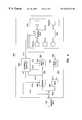
- FIG. 4is a block diagram of an illustrative embodiment of DRAM memory device 300 using input and output First-in-First-out (FIFO) buffers 330 , 332 according to the teachings of the present invention.
- the representation of DRAM 300has been simplified for purposes of illustrating the present invention and is not intended to be a complete description of all the features of a DRAM.
- the present inventionplaces dual FIFO buffers 330 , 332 directly on the same chip as DRAM 300 .
- DRAM device 300is compatible with memory slots 112 ( a-n ) illustrated in FIG. 2 .
- This dual FIFO 330 , 332 architectureallows read and write operations in DRAM memory banks 342 ( a-n ) to be decoupled from the external read and write operations associated with memory bus 120 . Decoupling increases system performance by allowing DRAM 300 operations to proceed at its natural speed while the operations associated with memory bus 120 proceed at its own natural speed. Varying bus widths between memory bus 120 and internal bus 420 are also compatible with the present invention. For example, high speed internal DRAM bus 420 may be eight bytes wide operating at a cycle rate N while memory bus 120 may operate at a cycle rate 4N (four times faster) but only providing two bytes per cycle. For example, the DRAM bus is eight bytes wide per cycle while operating at 33 MHZ while the external bus is two bytes per cycle wide while operating at 132 MHZ.
- Control logic, address and data information for DRAM 300 in FIG. 4is provided by individual inputs via data lines 202 , address lines 204 and various discrete lines to control logic 206 , as shown in FIG. 3 .
- This control logic, address and data informationis represented by memory bus 120 in FIG. 4 .
- FIFO buffers 330 , 332are coupled to memory bus 120 via multiplexer/demultiplexer 482 , 480 .
- Data to/from memory banks 342 ( a-n )are first buffered by FIFOs 330 , 332 through interfaces 380 , 382 .
- Single or multiple memory banks 342may be used with the present invention.
- Read and write operationsare separated between the two FIFOs 330 , 332 .
- Input FIFO 330performs write operations into memory banks 342 over interface 380 while output FIFO 332 performs read operations from memory banks 342 over interface 382 .
- FIFO buffers 330 , 332are not only intended to compensate for any mismatch that may exist between the rate at which data is produced and the rate at which it can be accepted, but to also allow greater flexibility to improve system performance of central processing unit 106 .
- prioritycan be assigned to internal read and write memory operations by controller 350 such that reads can be higher priority than writes. For example, if the memory device has both a read and a write command to execute, the write will be delayed in execution while the read is performed. This permits the spacing of writes in time such that they are performed when reads are not occurring or between reads in some optimum timed fashion. Alternatively, writes are prioritized higher than reads, or control of priority among reads and writes is set by an external device.
- memory bus 120represents control, data and address information for DRAM device 300 .
- the write data portion of memory bus 120is first directed to demultiplexer 480 over interface 400 .
- demultiplexer 480data is then written to FIFO 330 over interface 500 .
- FIFO 330buffers data until accepted by memory array 375 over interface 380 .
- data to be output from memory array 375 to memory bus 120is first directed to read FIFO 332 over interface 382 .
- Read FIFO 332buffers data until accepted by memory bus 120 .
- datais received over interface 502 for multiplexing by multiplexer 482 in order to interface memory bus 120 over connection 400 .
- Corresponding address and control informationis directed to controller 350 over interface 410 .
- Address and data bus information and control logic implementation, as illustrated in FIG. 4,is well known in the art.
- Controller 350interfaces with each of the key components to direct data to be read into or written out of memory banks 342 via the following interfaces: interface 412 to internal bus 420 , interface 414 , 416 to FIFOs 330 , 332 respectively, and interfaces 418 , 419 to demultiplexer 480 and multiplexer 482 , respectively. Since FIFOs 330 , 332 serve directly as a data buffer to memory array 375 , this permits processor 106 and memory bus 120 to operate at their natural frequencies.
- Optimum DRAM 300 performanceis achieved with the use of FIFOs 330 , 332 because memory read and write requests and procedures may be queued to allow high speed operation of memory array 375 .
- the present inventionmay also be used with a single bank 342 ( a ) as well as with an embedded memory interface in lieu of memory bus 120 .
- FIFOs 330 , 332buffer the data in serial lists until it can be used.
- the serial listsare stored in memory and require overhead to maintain them.
- These FIFO structurescan be implemented at many levels from all software to all hardware. The software implementations are often the most flexible but yield the lowest performance. The hardware implementations, while less flexible, give the highest performance.
- the present inventionis a fundamentally different architecture that couples a plurality of memory banks 342 sharing an internal bus in a DRAM memory device in array 375 to input and output FIFO buffers 330 , 332 .
- FIFOsthen interface directly with memory bus 120 .
- FIFO buffers 330 , 332function in either direction so that a computer system has the ability to que up numerous demands for reads and writes.
- This architecturepermits prioritization of reads over writes with prioritization governed by controller 350 such that if memory device 300 has both a read and a write command to execute, the write will be delayed in execution while the read is performed.
- controller 350provides prioritization commands such that memory reads would have priority over memory writes.
- This architecturealternatively allows prioritization of writes over reads or priority of reads and writes is established by an external device.
- FIFO buffers 330 , 332provide microprocessor 106 flexibility while appearing to operate at a very high speed. This architecture provides the capability for a number of memory banks 342 to operate in page mode and if latched together, system variability is provided on which to build from.
- FIFOs 330 , 332permits memory bus 120 to transmit and retrieve data with memory banks 342 at a natural communications speed while FIFOs 330 , 332 fill up at a rate dictated by the communications speed of memory banks 342 .
- FIFOs 330 , 332In order to successfully communicate at a different data rate, FIFOs 330 , 332 must be combined with multiplexer 482 and demultiplexer 480 .
- Multiplexer 482 and demultiplexer 480also permits communication over two different physical bus widths. Controller 350 controls multiplexer 482 and demultiplexer 480 for data width such that external data lines 202 have a speed and a bus width different than a bus width and a speed of internal communications bus 420 .
- external memory bus 120may physically exist as a narrower bus than the width of internal us 420 .
- the application of separate read and write FIFO buffers 330 , 332 interfaced with a plurality of memory banks 342 on a DRAM memory device 300compensates for mismatches in communications speed that may exist between the rate at which data is provided to memory banks 342 from memory bus 120 and the rate at which memory banks 342 can provide data to memory bus 120 .
- the present inventionis realized because input and output FIFOs 330 , 332 decouples internal DRAM 300 memory operations with external read and write operations associated memory bus 120 . Since FIFOs 330 , 332 serve directly as a data buffer to memory banks 342 , high speed computer operations is permitted because microprocessor 106 and memory bus 120 may operate at their own respective natural frequency without being restricted by the speed of DRAM memory device 300 . Decoupling of internal DRAM 300 memory operations with external reads and writes also permits prioritization of read and write commands by controller 350 . In lieu of memory bus 120 , DRAM 300 may interface directly with an embedded memory interface.
Landscapes
- Engineering & Computer Science (AREA)
- Theoretical Computer Science (AREA)
- Physics & Mathematics (AREA)
- General Engineering & Computer Science (AREA)
- General Physics & Mathematics (AREA)
- Dram (AREA)
Abstract
Description
Claims (95)
Priority Applications (1)
| Application Number | Priority Date | Filing Date | Title |
|---|---|---|---|
| US08/999,292US6622224B1 (en) | 1997-12-29 | 1997-12-29 | Internal buffered bus for a drum |
Applications Claiming Priority (1)
| Application Number | Priority Date | Filing Date | Title |
|---|---|---|---|
| US08/999,292US6622224B1 (en) | 1997-12-29 | 1997-12-29 | Internal buffered bus for a drum |
Publications (1)
| Publication Number | Publication Date |
|---|---|
| US6622224B1true US6622224B1 (en) | 2003-09-16 |
Family
ID=27805723
Family Applications (1)
| Application Number | Title | Priority Date | Filing Date |
|---|---|---|---|
| US08/999,292Expired - Fee RelatedUS6622224B1 (en) | 1997-12-29 | 1997-12-29 | Internal buffered bus for a drum |
Country Status (1)
| Country | Link |
|---|---|
| US (1) | US6622224B1 (en) |
Cited By (19)
| Publication number | Priority date | Publication date | Assignee | Title |
|---|---|---|---|---|
| US20030061447A1 (en)* | 2000-01-05 | 2003-03-27 | Perego Richard E. | Memory system including a point-to-point linked memory subsystem |
| US20040059879A1 (en)* | 2002-09-23 | 2004-03-25 | Rogers Paul L. | Access priority protocol for computer system |
| US20040186956A1 (en)* | 2000-01-05 | 2004-09-23 | Richard Perego | Configurable width buffered module |
| US20040228166A1 (en)* | 2003-03-07 | 2004-11-18 | Georg Braun | Buffer chip and method for actuating one or more memory arrangements |
| US6829689B1 (en)* | 2002-02-12 | 2004-12-07 | Nvidia Corporation | Method and system for memory access arbitration for minimizing read/write turnaround penalties |
| US20040256638A1 (en)* | 2000-01-05 | 2004-12-23 | Richard Perego | Configurable width buffered module having a bypass circuit |
| US20050010737A1 (en)* | 2000-01-05 | 2005-01-13 | Fred Ware | Configurable width buffered module having splitter elements |
| US20050007805A1 (en)* | 2000-01-05 | 2005-01-13 | Fred Ware | Configurable width buffered module having flyby elements |
| US20050044303A1 (en)* | 2000-01-05 | 2005-02-24 | Perego Richard E. | Memory system including an integrated circuit buffer device |
| US20050270892A1 (en)* | 2004-05-25 | 2005-12-08 | Stmicroelectronics S.R.I. | Synchronous memory device with reduced power consumption |
| US7404032B2 (en) | 2000-01-05 | 2008-07-22 | Rambus Inc. | Configurable width buffered module having switch elements |
| US7464225B2 (en) | 2005-09-26 | 2008-12-09 | Rambus Inc. | Memory module including a plurality of integrated circuit memory devices and a plurality of buffer devices in a matrix topology |
| US7562271B2 (en) | 2005-09-26 | 2009-07-14 | Rambus Inc. | Memory system topologies including a buffer device and an integrated circuit memory device |
| US20100306458A1 (en)* | 2009-06-02 | 2010-12-02 | Nokia Corporation | Memory device having integral instruction buffer |
| US9558840B2 (en)* | 2015-05-28 | 2017-01-31 | Kabushiki Kaisha Toshiba | Semiconductor device |
| WO2017222870A1 (en)* | 2016-06-22 | 2017-12-28 | Micron Technology, Inc. | Bank to bank data transfer |
| US10236038B2 (en) | 2017-05-15 | 2019-03-19 | Micron Technology, Inc. | Bank to bank data transfer |
| US11328764B2 (en) | 2005-09-26 | 2022-05-10 | Rambus Inc. | Memory system topologies including a memory die stack |
| CN116662254A (en)* | 2023-07-31 | 2023-08-29 | 广州中基国威电子科技有限公司 | On-chip high-speed bus architecture, data transmission method and embedded microprocessor |
Citations (28)
| Publication number | Priority date | Publication date | Assignee | Title |
|---|---|---|---|---|
| US4891794A (en) | 1988-06-20 | 1990-01-02 | Micron Technology, Inc. | Three port random access memory |
| US5029124A (en)* | 1988-05-17 | 1991-07-02 | Digital Equipment Corporation | Method and apparatus for providing high speed parallel transfer of bursts of data |
| US5072420A (en)* | 1989-03-16 | 1991-12-10 | Western Digital Corporation | FIFO control architecture and method for buffer memory access arbitration |
| US5146592A (en)* | 1987-09-14 | 1992-09-08 | Visual Information Technologies, Inc. | High speed image processing computer with overlapping windows-div |
| US5313624A (en)* | 1991-05-14 | 1994-05-17 | Next Computer, Inc. | DRAM multiplexer |
| US5361003A (en) | 1993-01-14 | 1994-11-01 | Micron Semiconductor, Inc. | Adjustable buffer driver |
| US5398325A (en)* | 1992-05-07 | 1995-03-14 | Sun Microsystems, Inc. | Methods and apparatus for improving cache consistency using a single copy of a cache tag memory in multiple processor computer systems |
| US5469558A (en)* | 1991-08-16 | 1995-11-21 | Multichip Technology | Dynamically reconfigurable memory system with programmable controller and FIFO buffered data channels |
| US5490260A (en)* | 1990-12-14 | 1996-02-06 | Ceram, Inc. | Solid-state RAM data storage for virtual memory computer using fixed-sized swap pages with selective compressed/uncompressed data store according to each data size |
| US5555429A (en) | 1989-03-09 | 1996-09-10 | Micron Technology, Inc. | Multiport RAM based multiprocessor |
| US5561466A (en)* | 1993-06-23 | 1996-10-01 | Nec Corporation | Video and audio data multiplexing into ATM cells with no dummy cell used and ATM cell demultiplexing |
| US5611075A (en)* | 1994-10-04 | 1997-03-11 | Analog Devices, Inc. | Bus architecture for digital signal processor allowing time multiplexed access to memory banks |
| US5615355A (en)* | 1992-10-22 | 1997-03-25 | Ampex Corporation | Method and apparatus for buffering a user application from the timing requirements of a DRAM |
| US5666494A (en)* | 1995-03-31 | 1997-09-09 | Samsung Electronics Co., Ltd. | Queue management mechanism which allows entries to be processed in any order |
| US5675749A (en)* | 1995-06-02 | 1997-10-07 | Motorola, Inc. | Method and apparatus for controlling show cycles in a data processing system |
| US5784705A (en)* | 1996-07-15 | 1998-07-21 | Mosys, Incorporated | Method and structure for performing pipeline burst accesses in a semiconductor memory |
| US5799209A (en)* | 1995-12-29 | 1998-08-25 | Chatter; Mukesh | Multi-port internally cached DRAM system utilizing independent serial interfaces and buffers arbitratively connected under a dynamic configuration |
| US5822772A (en)* | 1996-03-22 | 1998-10-13 | Industrial Technology Research Institute | Memory controller and method of memory access sequence recordering that eliminates page miss and row miss penalties |
| US5838603A (en)* | 1994-10-11 | 1998-11-17 | Matsushita Electric Industrial Co., Ltd. | Semiconductor device and method for fabricating the same, memory core chip and memory peripheral circuit chip |
| US5884099A (en)* | 1996-05-31 | 1999-03-16 | Sun Microsystems, Inc. | Control circuit for a buffer memory to transfer data between systems operating at different speeds |
| US5901100A (en)* | 1997-04-01 | 1999-05-04 | Ramtron International Corporation | First-in, first-out integrated circuit memory device utilizing a dynamic random access memory array for data storage implemented in conjunction with an associated static random access memory cache |
| US5905876A (en)* | 1996-12-16 | 1999-05-18 | Intel Corporation | Queue ordering for memory and I/O transactions in a multiple concurrent transaction computer system |
| US5923895A (en)* | 1996-11-15 | 1999-07-13 | Cirrus Logic, Inc. | Method and arrangement to effectively retrieve residual data from a buffer |
| US5925142A (en)* | 1995-10-06 | 1999-07-20 | Micron Technology, Inc. | Self-test RAM using external synchronous clock |
| US5978891A (en)* | 1994-01-21 | 1999-11-02 | Hitachi, Ltd. | Memory for operating synchronously with clock signals generated internally responsive to externally received control signals while outputting the clock signals via an external terminal |
| US6005823A (en)* | 1997-06-20 | 1999-12-21 | Micron Technology, Inc. | Memory device with pipelined column address path |
| US6044416A (en)* | 1997-09-19 | 2000-03-28 | Samsung Electronics Co., Ltd. | Configurable first-in first-out memory interface |
| US6161165A (en)* | 1996-11-14 | 2000-12-12 | Emc Corporation | High performance data path with XOR on the fly |
- 1997
- 1997-12-29USUS08/999,292patent/US6622224B1/ennot_activeExpired - Fee Related
Patent Citations (28)
| Publication number | Priority date | Publication date | Assignee | Title |
|---|---|---|---|---|
| US5146592A (en)* | 1987-09-14 | 1992-09-08 | Visual Information Technologies, Inc. | High speed image processing computer with overlapping windows-div |
| US5029124A (en)* | 1988-05-17 | 1991-07-02 | Digital Equipment Corporation | Method and apparatus for providing high speed parallel transfer of bursts of data |
| US4891794A (en) | 1988-06-20 | 1990-01-02 | Micron Technology, Inc. | Three port random access memory |
| US5555429A (en) | 1989-03-09 | 1996-09-10 | Micron Technology, Inc. | Multiport RAM based multiprocessor |
| US5072420A (en)* | 1989-03-16 | 1991-12-10 | Western Digital Corporation | FIFO control architecture and method for buffer memory access arbitration |
| US5490260A (en)* | 1990-12-14 | 1996-02-06 | Ceram, Inc. | Solid-state RAM data storage for virtual memory computer using fixed-sized swap pages with selective compressed/uncompressed data store according to each data size |
| US5313624A (en)* | 1991-05-14 | 1994-05-17 | Next Computer, Inc. | DRAM multiplexer |
| US5469558A (en)* | 1991-08-16 | 1995-11-21 | Multichip Technology | Dynamically reconfigurable memory system with programmable controller and FIFO buffered data channels |
| US5398325A (en)* | 1992-05-07 | 1995-03-14 | Sun Microsystems, Inc. | Methods and apparatus for improving cache consistency using a single copy of a cache tag memory in multiple processor computer systems |
| US5615355A (en)* | 1992-10-22 | 1997-03-25 | Ampex Corporation | Method and apparatus for buffering a user application from the timing requirements of a DRAM |
| US5361003A (en) | 1993-01-14 | 1994-11-01 | Micron Semiconductor, Inc. | Adjustable buffer driver |
| US5561466A (en)* | 1993-06-23 | 1996-10-01 | Nec Corporation | Video and audio data multiplexing into ATM cells with no dummy cell used and ATM cell demultiplexing |
| US5978891A (en)* | 1994-01-21 | 1999-11-02 | Hitachi, Ltd. | Memory for operating synchronously with clock signals generated internally responsive to externally received control signals while outputting the clock signals via an external terminal |
| US5611075A (en)* | 1994-10-04 | 1997-03-11 | Analog Devices, Inc. | Bus architecture for digital signal processor allowing time multiplexed access to memory banks |
| US5838603A (en)* | 1994-10-11 | 1998-11-17 | Matsushita Electric Industrial Co., Ltd. | Semiconductor device and method for fabricating the same, memory core chip and memory peripheral circuit chip |
| US5666494A (en)* | 1995-03-31 | 1997-09-09 | Samsung Electronics Co., Ltd. | Queue management mechanism which allows entries to be processed in any order |
| US5675749A (en)* | 1995-06-02 | 1997-10-07 | Motorola, Inc. | Method and apparatus for controlling show cycles in a data processing system |
| US5925142A (en)* | 1995-10-06 | 1999-07-20 | Micron Technology, Inc. | Self-test RAM using external synchronous clock |
| US5799209A (en)* | 1995-12-29 | 1998-08-25 | Chatter; Mukesh | Multi-port internally cached DRAM system utilizing independent serial interfaces and buffers arbitratively connected under a dynamic configuration |
| US5822772A (en)* | 1996-03-22 | 1998-10-13 | Industrial Technology Research Institute | Memory controller and method of memory access sequence recordering that eliminates page miss and row miss penalties |
| US5884099A (en)* | 1996-05-31 | 1999-03-16 | Sun Microsystems, Inc. | Control circuit for a buffer memory to transfer data between systems operating at different speeds |
| US5784705A (en)* | 1996-07-15 | 1998-07-21 | Mosys, Incorporated | Method and structure for performing pipeline burst accesses in a semiconductor memory |
| US6161165A (en)* | 1996-11-14 | 2000-12-12 | Emc Corporation | High performance data path with XOR on the fly |
| US5923895A (en)* | 1996-11-15 | 1999-07-13 | Cirrus Logic, Inc. | Method and arrangement to effectively retrieve residual data from a buffer |
| US5905876A (en)* | 1996-12-16 | 1999-05-18 | Intel Corporation | Queue ordering for memory and I/O transactions in a multiple concurrent transaction computer system |
| US5901100A (en)* | 1997-04-01 | 1999-05-04 | Ramtron International Corporation | First-in, first-out integrated circuit memory device utilizing a dynamic random access memory array for data storage implemented in conjunction with an associated static random access memory cache |
| US6005823A (en)* | 1997-06-20 | 1999-12-21 | Micron Technology, Inc. | Memory device with pipelined column address path |
| US6044416A (en)* | 1997-09-19 | 2000-03-28 | Samsung Electronics Co., Ltd. | Configurable first-in first-out memory interface |
Cited By (73)
| Publication number | Priority date | Publication date | Assignee | Title |
|---|---|---|---|---|
| US7010642B2 (en) | 2000-01-05 | 2006-03-07 | Rambus Inc. | System featuring a controller device and a memory module that includes an integrated circuit buffer device and a plurality of integrated circuit memory devices |
| US7206897B2 (en) | 2000-01-05 | 2007-04-17 | Rambus Inc. | Memory module having an integrated circuit buffer device |
| US20040186956A1 (en)* | 2000-01-05 | 2004-09-23 | Richard Perego | Configurable width buffered module |
| US7523248B2 (en) | 2000-01-05 | 2009-04-21 | Rambus Inc. | System having a controller device, a buffer device and a plurality of memory devices |
| US20030061447A1 (en)* | 2000-01-05 | 2003-03-27 | Perego Richard E. | Memory system including a point-to-point linked memory subsystem |
| US20040256638A1 (en)* | 2000-01-05 | 2004-12-23 | Richard Perego | Configurable width buffered module having a bypass circuit |
| US20050010737A1 (en)* | 2000-01-05 | 2005-01-13 | Fred Ware | Configurable width buffered module having splitter elements |
| US20050007805A1 (en)* | 2000-01-05 | 2005-01-13 | Fred Ware | Configurable width buffered module having flyby elements |
| US20050044303A1 (en)* | 2000-01-05 | 2005-02-24 | Perego Richard E. | Memory system including an integrated circuit buffer device |
| US20050041504A1 (en)* | 2000-01-05 | 2005-02-24 | Perego Richard E. | Method of operating a memory system including an integrated circuit buffer device |
| US20050156934A1 (en)* | 2000-01-05 | 2005-07-21 | Perego Richard E. | System featuring memory modules that include an integrated circuit buffer devices |
| US7404032B2 (en) | 2000-01-05 | 2008-07-22 | Rambus Inc. | Configurable width buffered module having switch elements |
| US7000062B2 (en) | 2000-01-05 | 2006-02-14 | Rambus Inc. | System and method featuring a controller device and a memory module that includes an integrated circuit buffer device and a plurality of integrated circuit memory devices |
| US7003618B2 (en) | 2000-01-05 | 2006-02-21 | Rambus Inc. | System featuring memory modules that include an integrated circuit buffer devices |
| US7363422B2 (en) | 2000-01-05 | 2008-04-22 | Rambus Inc. | Configurable width buffered module |
| US7526597B2 (en) | 2000-01-05 | 2009-04-28 | Rambus Inc. | Buffered memory having a control bus and dedicated data lines |
| US7320047B2 (en) | 2000-01-05 | 2008-01-15 | Rambus Inc. | System having a controller device, a buffer device and a plurality of memory devices |
| US7356639B2 (en) | 2000-01-05 | 2008-04-08 | Rambus Inc. | Configurable width buffered module having a bypass circuit |
| US7200710B2 (en) | 2000-01-05 | 2007-04-03 | Rambus Inc. | Buffer device and method of operation in a buffer device |
| US7206896B2 (en) | 2000-01-05 | 2007-04-17 | Rambus Inc. | Integrated circuit buffer device |
| US7017002B2 (en) | 2000-01-05 | 2006-03-21 | Rambus, Inc. | System featuring a master device, a buffer device and a plurality of integrated circuit memory devices |
| US7266634B2 (en) | 2000-01-05 | 2007-09-04 | Rambus Inc. | Configurable width buffered module having flyby elements |
| US7051151B2 (en) | 2000-01-05 | 2006-05-23 | Rambus Inc. | Integrated circuit buffer device |
| US7080194B1 (en) | 2002-02-12 | 2006-07-18 | Nvidia Corporation | Method and system for memory access arbitration for minimizing read/write turnaround penalties |
| US6829689B1 (en)* | 2002-02-12 | 2004-12-07 | Nvidia Corporation | Method and system for memory access arbitration for minimizing read/write turnaround penalties |
| US20040059879A1 (en)* | 2002-09-23 | 2004-03-25 | Rogers Paul L. | Access priority protocol for computer system |
| US7447805B2 (en)* | 2003-03-07 | 2008-11-04 | Infineon Technologies Ag | Buffer chip and method for controlling one or more memory arrangements |
| US20040228166A1 (en)* | 2003-03-07 | 2004-11-18 | Georg Braun | Buffer chip and method for actuating one or more memory arrangements |
| US7366012B2 (en)* | 2004-05-25 | 2008-04-29 | Stmicroelectronics S.R.L. | Synchronous memory device with reduced power consumption |
| US20050270892A1 (en)* | 2004-05-25 | 2005-12-08 | Stmicroelectronics S.R.I. | Synchronous memory device with reduced power consumption |
| US8539152B2 (en) | 2005-09-26 | 2013-09-17 | Rambus Inc. | Memory system topologies including a buffer device and an integrated circuit memory device |
| US10381067B2 (en) | 2005-09-26 | 2019-08-13 | Rambus Inc. | Memory system topologies including a buffer device and an integrated circuit memory device |
| US7685364B2 (en) | 2005-09-26 | 2010-03-23 | Rambus Inc. | Memory system topologies including a buffer device and an integrated circuit memory device |
| US7729151B2 (en) | 2005-09-26 | 2010-06-01 | Rambus Inc. | System including a buffered memory module |
| US12394471B2 (en) | 2005-09-26 | 2025-08-19 | Rambus Inc. | Memory system topologies including a memory die stack |
| US11727982B2 (en) | 2005-09-26 | 2023-08-15 | Rambus Inc. | Memory system topologies including a memory die stack |
| US8108607B2 (en) | 2005-09-26 | 2012-01-31 | Rambus Inc. | Memory system topologies including a buffer device and an integrated circuit memory device |
| US7464225B2 (en) | 2005-09-26 | 2008-12-09 | Rambus Inc. | Memory module including a plurality of integrated circuit memory devices and a plurality of buffer devices in a matrix topology |
| US11328764B2 (en) | 2005-09-26 | 2022-05-10 | Rambus Inc. | Memory system topologies including a memory die stack |
| US9117035B2 (en) | 2005-09-26 | 2015-08-25 | Rambus Inc. | Memory system topologies including a buffer device and an integrated circuit memory device |
| US11043258B2 (en) | 2005-09-26 | 2021-06-22 | Rambus Inc. | Memory system topologies including a memory die stack |
| US9563583B2 (en) | 2005-09-26 | 2017-02-07 | Rambus Inc. | Memory system topologies including a buffer device and an integrated circuit memory device |
| US10672458B1 (en) | 2005-09-26 | 2020-06-02 | Rambus Inc. | Memory system topologies including a buffer device and an integrated circuit memory device |
| US10535398B2 (en) | 2005-09-26 | 2020-01-14 | Rambus Inc. | Memory system topologies including a buffer device and an integrated circuit memory device |
| US7562271B2 (en) | 2005-09-26 | 2009-07-14 | Rambus Inc. | Memory system topologies including a buffer device and an integrated circuit memory device |
| US9865329B2 (en) | 2005-09-26 | 2018-01-09 | Rambus Inc. | Memory system topologies including a buffer device and an integrated circuit memory device |
| WO2010139850A1 (en)* | 2009-06-02 | 2010-12-09 | Nokia Corporation | Memory device having integral instruction buffer |
| US8713248B2 (en)* | 2009-06-02 | 2014-04-29 | Nokia Corporation | Memory device and method for dynamic random access memory having serial interface and integral instruction buffer |
| US20100306458A1 (en)* | 2009-06-02 | 2010-12-02 | Nokia Corporation | Memory device having integral instruction buffer |
| US10026485B2 (en) | 2015-05-28 | 2018-07-17 | Toshiba Memory Corporation | Semiconductor device |
| US12100459B2 (en) | 2015-05-28 | 2024-09-24 | Kioxia Corporation | Semiconductor device |
| US11715529B2 (en) | 2015-05-28 | 2023-08-01 | Kioxia Corporation | Semiconductor device |
| US9558840B2 (en)* | 2015-05-28 | 2017-01-31 | Kabushiki Kaisha Toshiba | Semiconductor device |
| US10438670B2 (en) | 2015-05-28 | 2019-10-08 | Toshiba Memory Corporation | Semiconductor device |
| US9754676B2 (en)* | 2015-05-28 | 2017-09-05 | Toshiba Memory Corporation | Semiconductor device |
| US10636499B2 (en) | 2015-05-28 | 2020-04-28 | Toshiba Memory Corporation | Semiconductor device |
| US20170103816A1 (en)* | 2015-05-28 | 2017-04-13 | Kabushiki Kaisha Toshiba | Semiconductor device |
| US20180294038A1 (en) | 2015-05-28 | 2018-10-11 | Toshiba Memory Corporation | Semiconductor device |
| US11295821B2 (en) | 2015-05-28 | 2022-04-05 | Kioxia Corporation | Semiconductor device |
| US10950314B2 (en) | 2015-05-28 | 2021-03-16 | Toshiba Memory Corporation | Semiconductor device |
| US10387046B2 (en) | 2016-06-22 | 2019-08-20 | Micron Technology, Inc. | Bank to bank data transfer |
| US10929023B2 (en) | 2016-06-22 | 2021-02-23 | Micron Technology, Inc. | Bank to bank data transfer |
| WO2017222870A1 (en)* | 2016-06-22 | 2017-12-28 | Micron Technology, Inc. | Bank to bank data transfer |
| TWI661310B (en)* | 2016-06-22 | 2019-06-01 | 美光科技公司 | Apparatus and method for operating a memory device |
| US11755206B2 (en) | 2016-06-22 | 2023-09-12 | Micron Technology, Inc. | Bank to bank data transfer |
| CN109416918A (en)* | 2016-06-22 | 2019-03-01 | 美光科技公司 | Library-to-library data transfer |
| US12393341B2 (en) | 2016-06-22 | 2025-08-19 | Lodestar Licensing Group Llc | Bank to bank data transfer |
| US10796736B2 (en) | 2017-05-15 | 2020-10-06 | Micron Technology, Inc. | Bank to bank data transfer |
| US11514957B2 (en) | 2017-05-15 | 2022-11-29 | Micron Technology, Inc. | Bank to bank data transfer |
| US10236038B2 (en) | 2017-05-15 | 2019-03-19 | Micron Technology, Inc. | Bank to bank data transfer |
| US12183418B2 (en) | 2017-05-15 | 2024-12-31 | Lodestar Licensing Group Llc | Bank to bank data transfer |
| CN116662254A (en)* | 2023-07-31 | 2023-08-29 | 广州中基国威电子科技有限公司 | On-chip high-speed bus architecture, data transmission method and embedded microprocessor |
| CN116662254B (en)* | 2023-07-31 | 2024-02-23 | 广州中基国威电子科技有限公司 | On-chip high-speed bus architecture, data transmission method and embedded microprocessor |
Similar Documents
| Publication | Publication Date | Title |
|---|---|---|
| US6622224B1 (en) | Internal buffered bus for a drum | |
| US7136958B2 (en) | Multiple processor system and method including multiple memory hub modules | |
| US6418077B1 (en) | Memory access methods and devices for use with random access memories | |
| KR100272072B1 (en) | High performance, high bandwidth memory bus architecture utilizing sdrams | |
| US6876589B2 (en) | Method and apparatus for supplementary command bus | |
| US20250139026A1 (en) | Memory module with reduced read/write turnaround overhead | |
| US6473838B1 (en) | Data transfer system for multiple network processors using dual DRAM storage | |
| US20030018845A1 (en) | Memory device having different burst order addressing for read and write operations | |
| US9696941B1 (en) | Memory system including memory buffer | |
| US6459647B1 (en) | Split-bank architecture for high performance SDRAMs | |
| US6502173B1 (en) | System for accessing memory and method therefore | |
| KR101086417B1 (en) | Partial Access Device and Method of Dynamic Random Access Memory | |
| US7774535B2 (en) | Memory system and memory device | |
| JP3384770B2 (en) | High bandwidth narrow I/O memory device with command stacking - Patents.com | |
| US8244929B2 (en) | Data processing apparatus | |
| US20250139022A1 (en) | Multiplexed bus streak management | |
| WO2025101757A1 (en) | Memory apparatus and method for improved write-read turnaround times | |
| JPH0573470A (en) | Dual port storage device |
Legal Events
| Date | Code | Title | Description |
|---|---|---|---|
| AS | Assignment | Owner name:MICRON TECHNOLOGY, INC., IDAHO Free format text:ASSIGNMENT OF ASSIGNORS INTEREST;ASSIGNOR:CLOUD, EUGENE H.;REEL/FRAME:008925/0028 Effective date:19971219 | |
| FEPP | Fee payment procedure | Free format text:PAYOR NUMBER ASSIGNED (ORIGINAL EVENT CODE: ASPN); ENTITY STATUS OF PATENT OWNER: LARGE ENTITY | |
| CC | Certificate of correction | ||
| FPAY | Fee payment | Year of fee payment:4 | |
| AS | Assignment | Owner name:ROUND ROCK RESEARCH, LLC,NEW YORK Free format text:ASSIGNMENT OF ASSIGNORS INTEREST;ASSIGNOR:MICRON TECHNOLOGY, INC.;REEL/FRAME:023786/0416 Effective date:20091223 Owner name:ROUND ROCK RESEARCH, LLC, NEW YORK Free format text:ASSIGNMENT OF ASSIGNORS INTEREST;ASSIGNOR:MICRON TECHNOLOGY, INC.;REEL/FRAME:023786/0416 Effective date:20091223 | |
| FPAY | Fee payment | Year of fee payment:8 | |
| REMI | Maintenance fee reminder mailed | ||
| LAPS | Lapse for failure to pay maintenance fees | ||
| STCH | Information on status: patent discontinuation | Free format text:PATENT EXPIRED DUE TO NONPAYMENT OF MAINTENANCE FEES UNDER 37 CFR 1.362 | |
| FP | Lapsed due to failure to pay maintenance fee | Effective date:20150916 |