US6621275B2 - Time resolved non-invasive diagnostics system - Google Patents
Time resolved non-invasive diagnostics systemDownload PDFInfo
- Publication number
- US6621275B2 US6621275B2US09/995,548US99554801AUS6621275B2US 6621275 B2US6621275 B2US 6621275B2US 99554801 AUS99554801 AUS 99554801AUS 6621275 B2US6621275 B2US 6621275B2
- Authority
- US
- United States
- Prior art keywords
- chip
- collection
- optics
- cooling
- dut
- Prior art date
- Legal status (The legal status is an assumption and is not a legal conclusion. Google has not performed a legal analysis and makes no representation as to the accuracy of the status listed.)
- Expired - Lifetime, expires
Links
Images


Classifications
- G—PHYSICS
- G01—MEASURING; TESTING
- G01N—INVESTIGATING OR ANALYSING MATERIALS BY DETERMINING THEIR CHEMICAL OR PHYSICAL PROPERTIES
- G01N21/00—Investigating or analysing materials by the use of optical means, i.e. using sub-millimetre waves, infrared, visible or ultraviolet light
- G01N21/84—Systems specially adapted for particular applications
- G—PHYSICS
- G01—MEASURING; TESTING
- G01R—MEASURING ELECTRIC VARIABLES; MEASURING MAGNETIC VARIABLES
- G01R31/00—Arrangements for testing electric properties; Arrangements for locating electric faults; Arrangements for electrical testing characterised by what is being tested not provided for elsewhere
- G01R31/28—Testing of electronic circuits, e.g. by signal tracer
- G01R31/302—Contactless testing
- G01R31/308—Contactless testing using non-ionising electromagnetic radiation, e.g. optical radiation
- G01R31/311—Contactless testing using non-ionising electromagnetic radiation, e.g. optical radiation of integrated circuits
Definitions
- the present inventionrelates to a system for in-situ transistor level measurement of circuit timing information directly related to the switching events (logic transitions) of switching events of transistors of electrically active semiconductor integrated circuits.
- CMOScomplementary meal oxide semiconductor
- the current “pulse”coincides (in-time and characteristics) directly with the voltage transition responsible for the change in the state (logic) of the device.
- CMOScomplementary meal oxide semiconductor
- the hot-electron emissions from electrically active semiconductor transistor devicesto study the behavior and response of the device to electrical currents and the temporal relations of the current pulses with respect to each other.
- Khurana et al.demonstrated that photoluminescence hot-carrier emission coincides in time and characteristics with the current pulse and thereby the voltage switching of a transistor, thereby teaching that, in addition to failure analysis (location of“hot-spots” where the device may be drawing current in excess of its design), the phenomenon can also be used for obtaining circuit timing information (switching) and therefore used for IC device debug and circuit design. See, also, U.S. Pat. No. 5,940,545 to Kash et al., disclosing a system for such an investigation.
- the light emission in semiconductor devicesis very faint. Accordingly, various optical and detection schemes have been proposed to more efficiently collect the emission and reduce the noise, i.e., increase collection fidelity, bandwidth, and speed of the collection and detection system.
- MCPsmicrochannel photomultipliers
- APDsavalanche photodiodes
- TACtime-to-amplitude converter
- NAnumerical aperture
- One historical method for increasing “n”is to fill the air gap between a properly aberration corrected objective lens and the sample with an index matching oil that matches the index of refraction of the object.
- proper matching fluidsare not available to achieve the index matching
- other methodscan be used, such as the use of a solid immersion lens (matching the material of the sample) placed between the object and the objective lens.
- immersion lens and index matching fluidare disclosed in, for example, U.S. Pat. Nos. 3,524,694, 3,711,186, and 3,912,378. More modem discussions of immersion lenses can be found in U.S. Pat. Nos.
- flipchip packaged devicesare ones that are packaged in flipchip format.
- the direct attachment between the IC device and package carrieralleviates the use of wire bonding of the IC “chip” to the carrier.
- the transistorsare readily accessible through the substrate and therefore are not “masked” by the multiple layers of metal interconnect. Since the build, implementation and structure of flip chip packaged devices are well known; it will not be discussed here in details. Information relating to flip chip can be found in, for example, http://www.flipchip.com and http://world.std.com/ ⁇ hycomp/flippage.html.
- the present inventorsprovide a commercially viable integrated system for IC device debug by time resolved measurements of hot electron photo emission, providing high spatial resolution imaging and high temporal resolution detection. Moreover, the system enables cooling and temperature control of the device under test (DUT). Furthermore, the system enables navigation and imaging using the IC computer-aided design (CAD) layout. The inventive system is particularly useful for testing and debugging functional semiconductor integrated circuits having operational currents flowing therein.
- an integrated system for testing an integrated circuit chipis provided.
- the chip under testis coupled to an Automated Test Equipment (ATE) that powers the device and stimulates it with programmed logic vectors and signals to simulate operating (functional & test) conditions of the chip.
- ATEAutomated Test Equipment
- the inventive systemcomprises a controller receiving sync signals from the ATE; an optical imaging system for selectively imaging selected devices of the chip; a collection system for collecting photoemission from the chip and providing a time-resolved signal indicative of the photoemissions; an optomechanical navigation system for orienting the optical imaging system and the collection system with respect to the selected devices; and a thermal management system for cooling the chip to a temperature designated by the controller.
- the inventive systemcomprises an x-y-z stage that is used to move the optics to the location of interest on the device under test, and focus and image the device(s) of interest.
- the navigationis performed in relation to a CAD layout of the IC.
- a mechanized shutteris used to variably define imaging areas within the field of view of the optics.
- the deviceis illuminated and is imaged with an image intensifier, thereby providing high spatial resolution.
- the illumination sourceis turned off and the device is stimulated with test signals.
- hot electron photoemissionis collected by the optics and is imaged onto a fiber optics.
- emission detectionis synchronized with the test signals, i.e., the automated test equipment (ATE).
- ATEautomated test equipment
- Light collected by the fiber opticsis detected by an avalanche photodiode (APD), which is coupled to an avalanche quenching circuit, a time-to-amplitude converter (TAC), and a multi-channel analyzer.
- APDavalanche photodiode
- TACtime-to-amplitude converter
- the APDis gated so that it assumes the detection condition only just before a light emission is expected according to the sync signal from the ATE. This provides reduction in noise and increases the life of the APD.
- One advantageous feature of the inventive systemis the active temperature control of the DUT.
- the inventive systemenables testing of the DUT at various controlled temperatures. Temperature control is provided separately to the chamber's interior and the DUT, and integrated with the optical imaging/detection system.
- cooling of the DUTis done using a cooling block with cooling fluid circulated therein.
- the DUTis cooled using liquid micro-spray cooling technique.
- an immersion lensis used to increase the light collection efficiency and imaging resolution.
- the index matched immersion lensis bi-convex and is pressured onto the DUT during emission detection to ensure direct (no air-gap) contact with the DUT.
- an autofocusmay also be provided for enhanced stability of the system.
- the autofocusis a passive system, i.e., includes no illumination source, but rather uses a feedback loop optimizing the collection rate of the photoemission light.
- FIGS. 1-1Bare general schematics depicting the major components of the testing and debug system according to an embodiment of the invention.
- FIG. 1Cdepicts the major component of another embodiment of the inventive testing and debug system.
- FIG. 2Adepicts an embodiment of the cooling plate in a top view
- FIG. 2Bis a cross section along lines A—A in FIG. 2 A.
- FIG. 3depicts an embodiment of the inventive immersion lens.
- FIG. 4depicts another embodiment of the inventive system, using laser scanning microscope for imaging.
- FIG. 5exemplifies an embodiment for a “pick and place” system for locating the immersion lens at the appropriate target location.
- FIG. 6depicts another embodiment of the present invention.
- FIGS. 7-9exemplify various setups of embodiments of the invention.
- FIG. 10depicts an embodiment of the inventive microscope objective/DUT crash protection system.
- FIG. 11depicts an embodiment of the inventive micro-spray cooling.
- FIG. 12depicts another embodiment of the present invention.
- FIG. 13depicts an embodiment of the inventive micro-spray cooling having dual-lens in registration.
- FIG. 14exemplifies a high-speed time resolve emission detection scheme according to an embodiment of the present invention.
- the present inventionprovides a testing system particularly suitable for rise time, timing; logic fault localization and other testing of microchips, especially from the backside through the substrate (e.g., flip chip packaged devices). Accordingly, the description proceeds with examples using flip chip. However, it should be appreciated that the invention is not limited to testing flip chips. For example, it is possible to take top-side packaged devices and “flip” them in a chip-scale package (CSP), or design the proper opening to ensure the emitted light gets through the top-side. What is desired is to be able to collect emission from a device of interest in the chip.
- CSPchip-scale package
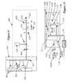
- FIGS. 1A and 1Bare general schematics depicting the major components of the testing and debug system according to an exemplary embodiment of the invention.
- the systemoperates in conjunction with a commercially available automated testing equipment 105 (ATE).
- ATEgenerally comprises a controller, such as a pre-programmed computer 181 , and a test head 124 , which comprises an adapter 125 used to deliver signals generated by the controller 181 to the DUT 110 (FIG. 1B) in a manner well known in the art.
- the ATEis used to generate signals that stimulate the DUT to perform various tasks, as designed by the chip designer to check and/or debug the chip.
- the various signals generated by the controller 181are delivered to the DUT via the adapter 125 .
- the adapter 125may include a space transformer, a DUT load board and a DUT socket, in a manner well known in the art.
- the ATE test headis placed on top of a vibration isolated test bench 115 , while the chamber 100 that houses the entire optics, imaging and sensing system, and an X-Y-Z stage 175 , is situated below.
- Thisprovides a tremendous advantage as it allows the system to be used with any type and size of ATE without interference with, or making modification to any of the elements inside chamber 100 .
- the ATEis used to place the DUT from above, so that it is visible to the optics 120 via opening 185 .
- Stage 175enables placing of the collecting optics at any locations within the opening 185 . While and X-Y-Z stage is used in this example, it should be apparent that other stages can be used to enable placement of the optics at an indicated location within opening 185 .
- an illumination source 130is used to illuminate the DUT.
- Illumination source 130emits light in the infrared (IR) range using, for example, an IR laser, or photodiode , or a tungsten-halogen lamp. The light is focused through the microscope objective onto and then reflects from the DUT and beam splitter 160 .
- IRinfrared
- the imager 145can be any two-dimensional detector capable of imaging in the infrared range, such as, for example, an intensifier vidicon, or InGaAs array.
- IR vidiconsare commercially available from, for example, Hamamatsu (http://usa.hamamatsu.com).
- the device of interestis fabricated on silicon.
- wavelengths shorter than IRare absorbed in silicon. Therefore, in this example the illumination and imaging is done in IR.
- a different wavelength illumination and imagingmay be used.
- Beam splitter mirror 165is used to deflect part of the collected light to the focusing system 140 .
- the overall imaging systemmay be connected to a Z-actuator 190 for auto-focusing purposes.
- an exemplary system for the auto-focusis described more fully below.
- the switchable mirror 135needs to be capable of selectively varying the optical path between the navigation and detection modes.
- mirror 135may be mechanically moved or rotated, or it may be made of an active element capable of variable reflectivity according to the selected mode so that, for example, in one mode it is totally reflective, while in the other mode it is totally transmissive.
- a substratemay be made having half of it transmissive and the other half reflective. Such a substrate can be provided with a rotating mechanism to insert in the optical path the reflective of transmissive part as desired.
- a mechanized aperture 170is provided at the image plane of the collection optics 120 , together with field lens 195 .
- the entrance pupil of collection optics 120is imaged by the field lens 195 onto the entranced plane of the focusing element of the detector in imager 145 .
- the pupil entrance of the collection opticsis imaged by the focusing element onto a fiber which couples the collected photons into the detector in imager 145 .
- a feature of the present inventionis that the illumination path takes place through the mechanized aperture 170 (which is positioned at the image plane of the collection optics) and thereby its opening defines the filed-of-view on the sample or device under test.
- the aperturealso defines the portions of the sample imaged onto the imager 145 . That is, depending on the particular test to be run, one may wish to select any particular section of the DUT for emission. Using information about the chip design and layout stored in CAD software, such as, for example, Cadence, and using navigation software, such as, for example, Merlin's Framework available from Knights Technology (wxvw.electroglass.com), one may select a particular device for emission test, and block the image and emission of the other devices in the field-of-view of the collection optics. When the user selects a device or location, the system activates the stage 175 so that the collection optics is centered on the selected device or location.
- the aperture 170may be adjusted to increase or decrease the field of view as appropriate for the particular test desired.
- mirror 135When an appropriate field of view has been set and an image obtained, mirror 135 is rotated so that the light path towards the IR sensitive detector 150 is established (opened). Additionally, light source 130 is shut off or blocked during testing. It should be appreciated, of course, that chamber 100 prevents any external light from reaching any of the optics, imagers and sensors enclosed within.
- a “probe area”is established by the area of the fiber core as it is imaged from the detector by the field lens and the collection optics onto the DUT.
- the diameter of this “probe area”is defined by the size of the fiber and the magnification defined by the focal lengths and distances of the optical train, the collection optics, field lens and the focusing optics at the fiber.
- Photon sensing during testingis done by detector 150 , which is, for example, an infrared sensor, such as a photomultiplier tube (PMT), a photocathode coupled to a multi-channel plate (MCP), an avalanche photodiode (APD), etc.
- the signal from the detector 150is sampled by the high-speed data acquisition electronics 155 .
- Electronics 155is described in more details below.
- Controller 180which may be a general-purpose computer running dedicated software, is used to control the various elements of the system, such as the actuators and stages and sampler.
- the controller 180receives sync signals from the ATE 105 .
- a feature of the inventive systemis that in testing mode focus is performed using the light emitted from the DUT. More specifically, the controller 180 performs photon counting of photon collected by the detector 150 at various Z positions. The Z position corresponding to the highest photon count is determined to be the focus position.
- FIG. 1Cdepicts an embodiment of the present invention using the general construction of the embodiment of FIG. 1B, except using a different arrangement of the optics and detectors inside chamber 100 .
- in the navigation mode switchable mirror 135 ′directs light from light source 130 ′ towards the DUT 110 ′.
- Light reflected from the DUTpasses through quarter-wave plate 162 and is deflected by polarizer mirror 160 ′ towards the imager.
- quarter-wave plate 162 ′ and polarizer mirror 106 ′can be replaced by a half mirror arrangement that is transparent to light from source 130 ′, but reflects light coming from DUT 110 ′.
- quarter-wave plate 162 ′ and polarizer mirror 106 ′can be replaced by a half mirror arrangement that is transparent to light from source 130 ′, but reflects light coming from DUT 110 ′.
- mechanized aperture 170 ′ with field lens 195 ′are provided at the image plane, and are illuminated from the back, so as to define the field of view. Also, in this embodiment the image obtained by the imager 145 ′ is used by the focus algorithm 140 ′. This is an advantageous arrangement since in this manner all the light reflected from the DUT 110 ′ is available to imager 145 ′ for creating the image.
- the mirror 135 ′is swung so that optical path to the IR sensitive detector 150 ′ is created. Additionally, the light source 130 ′ is preferably turned off. As can be understood, once the field of view was determined by the mechanized aperture during the navigation mode, it remains in the same position for the detection mode, thereby defining the field of view during the detection mode as well.
- One particular feature of the embodiments of the present inventionis the provision of integrated chip cooling. That is, in order to allow for full and accurate testing of the chip while simulating optimal operating environment, i.e., field conditions, the various embodiments of the invention provide for cooling and temperature control of the chip.
- various elementssuch as heat sinks and/or fans are provided in order to remove heat from the chip. Therefore, in the embodiments of the present invention various provisions are made in order to simulate such heat removal elements and allow for full and accurate testing.
- the systemenables active control of the temperature of the DUT in order to test the performance of the DUT with respect to various operating temperatures.
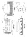
- FIG. 2Adepicts a first embodiment of heat removal system in the form of a cooling plate 210 in a top view
- FIG. 2Bis a cross section along lines A—A in FIG. 2 A.
- DUT 260is shown to include peripheral devices 265 for illustration purposes only. It would be appreciated that the system can also be used for inspection of DUT having no peripheral devices.
- the cooling plate 210is preferably made of synthetic diamond using known methods, such as CVD.
- Fluid conduits 220are provided on the top surface of the cooling plate 220 , and have inlet 250 and outlet 240 for cooling fluid circulation (the pump and other fluid circulation elements are not shown as they are fully known in the art).
- Cooling plate 210needs to have a window for imaging the target area on the DUT. While a single window is sufficient under most circumstances, as shown in FIG. 2B peripheral elements 265 may sometime restrict placement and movement of cooling plate 210 over the DUT. Therefore, in the depicted embodiment cooling plate 210 includes an array of windows 235 . Thus, for each target area on the DUT the appropriate window is selected and the collection optics 120 (shown in FIG. 2B in dashed lines) is aligned over the selected window using the x-y stage 175 . The cooling plate can be moved over the flip chip using the x-y actuators 280 , so that the window is aligned with a target area of the chip to be inspected.
- each window 235 of cooling plate 210has an immersion lens placed therein.
- the immersion lensmay be such as the ones disclosed in U.S. Pat. Nos. 5,004,307, 5,208,648 and 5,282,088, or any other suitable immersion lens.
- a novel bi-convex lensis used. This lens is shown in detail in FIG. 3, which is an enlarged area of one of the windows 235 of FIG. 2 B.
- the immersion lens of FIG. 3has a convex bottom surface 385 .
- the convex bottom surfaceis advantageous in that it allows for easier lateral and vertical movement of the cooling plate, since it avoids vacuum condition with the DUT. Additionally, it allows for easier placement of the focus plane i.e., easier alignment of the optical axes, over the location of interest. Moreover, it provides voids, which may assist in collecting excess index matching fluid when it is used.
- Another benefit of the bi-convex designis the ability to “press” with minimum force the immersion lens into the DUT to avoid having an air-gap between the immersion lens and the DUT.
- a conventional flat hemispherecannot avoid the air-gaps and if pressed will require much more force and may break the DUT.
- FIG. 3Another feature depicted in FIG. 3 is a center marking 375 provided on the center of the top surface of the immersion lens 370 .
- a markingmay be provided regardless of the type of immersion lens used. The marking is done to allow fast and accurate placement of the collection optics 120 over the immersion lens. That is, when the collection optics 120 is moved from one immersion lens to another, the marking facilitates fast acquisition and alignment of the objective of the collection optics with the target immersion lens.
- Controller 165is used to move the cooling plate, so that one of the windows is placed generally to expose the target area and its neighborhood.
- the systemis placed in a normal microscope mode, i.e., illumination source 130 is activated and the mirror 135 is inserted to provide a light path from the collection optics 120 to the imager 145 and focus 140 .
- Imager 145images the DUT through the appropriate window of the cooling plate and the collection optics.
- the illumination and imaging in the microscope modecan be done in bright-field mode, dark-field mode, or both. Bright filed and dark field illumination and imaging configurations are known in the art and, therefore, will not be detailed here.
- the controller 165activates the x-y stage to place the collection optics appropriately. Also, auto-focus 140 is used to control a Z-actuator so that the objective of collection optics 120 is focused on the target area of the DUT. Additionally, the area of interest within the field of view is defined using the aperture 170 .
- FIG. 4depicts another embodiment of the present invention.
- navigation and target acquisitionis performed using a confocal laser-scanning microscope (LSM) 400 .
- LSMlaser-scanning microscope
- General information regarding confocal scanning microscopescan be found in: Generalizing the Confocal Microscope via Heterodyne Interferometry and Digital Filtering, P. C. D. Hobbs and G. S. Kino, Journal of Microscopy, Vol. 130, Pt. 3, 1990, pp. 245-264; and U.S. Pat. No. 5,532,873. You may want to refer to Kino book, and drop Hobbs).
- LSM 400is engaged when the infrared laser diode 405 is activated as a light source and mirror 435 is positioned to complete the optical path from the laser diode 405 to the DUT, as shown by the solid-line image.
- the light beam from laser 405is scanned using scanner 430 , which may be, for example, an acousto-optic deflector (AOD) or a rotating multi-facetted mirror.
- scanner 430which may be, for example, an acousto-optic deflector (AOD) or a rotating multi-facetted mirror.
- AODacousto-optic deflector
- mirror 435is positioned to complete the optical path from the DUT to the detector 450 , as shown by the broken-line image.
- LSM 400In addition to laser diode 405 , LSM 400 generally comprises lens system 410 , which collects the light from the diode and directs it onto polarizer-mirror 425 and quarter-wave plate 415 . The light then enters one of the objectives 445 selected by the objective turret 465 . As exemplified in this embodiment, turret 465 carries three selectable objectives 445 , each with different magnification; however, either a single or other multiple objective arrangements may be provided. Light reflected from the DUT is then collected and directed by the polarizer-mirror 425 towards the detector 420 (e.g., vidicon or InGaAs detector).
- the detector 420e.g., vidicon or InGaAs detector
- Aberration correction ring 455is provided to compensate for varying thickness of the silicon. This is a particularly beneficial feature when observing through the backside of the chip.
- the solid immersion lens 460is also shown.
- the solid immersion lens 460may be bi-convex.
- the solid immersion lens 460can be used for final target imaging and for efficient emission collection.
- a “pick and place” systemis provided to position and land the immersion lens 460 at the appropriate target location.
- FIG. 5An embodiment of the pick and place system is exemplified in FIG. 5 .
- a microscope objective coupling housing 505is provided with an adjustable sleeve 510 that enables an airtight coupling to the housing 505 .
- the sleeveis placed over the immersion lens 560 .
- Valve 515is connected to an air pump so as to enable control of pressure in the chamber 520 defined by the immersion lens, the sleeve 510 , and the objective housing 505 . Reducing the pressure enables the operator to pick the lens 560 using vacuum forces. When the lens 560 is placed at the appropriate target location, the pressure can still be controlled to enable focusing.
- the distance between the coupling objective and the immersion lenscan be controlled in order to compensate for variations in the device thickness and aberration caused by the layers over the device.
- the pumpcan be used to create an elevated pressure in the chamber 520 to ensure good surface contact between the lens and the chip surface and avoid air gaps. It has been discovered by the present inventors that when a pressure slightly elevated above atmospheric pressure is provided on a bi-convex immersion lens, the thinned sample wafer “warps” about the lens, thereby enabling increased collection of light from the wafer, and avoiding the gaps (air) that degrade the index matching between the SIL and the sample (caused by surface non-uniformities) which ensures high NA and good coupling.
- FIG. 4Another feature exemplified in FIG. 4 in connection with the objective system is the provision of an active device cooling system 440 .
- a micro spray cooling systemis provided.
- the micro-spray cooling systemis described in more details below with reference to FIG. 11 .
- laser 405is switched off and mirror 435 is switched to the position shown in the broken-line image. In this position the light emitted and collected from the DUT is directed towards field lens 465 and the field of view is defined by mechanized aperture 470 placed in the image plane. Field lens 465 then projects the image onto the detector 450 .
- the ATEprovides the desired test vector to the DUT, while also providing synchronization signal to the system controller and detector electronics. Thus, when an emission (event) is detected, its relative “arrival” rime with respect to the synch signal is recorded to enable timing analysis of the performance of the DUT.
- FIG. 6depicts another embodiment of the present invention.
- the embodiment of FIG. 6includes two illumination sources.
- two alternate illumination sources, 605 and 671are provided for navigation, target acquisition, and imaging.
- camera 628is used for imaging via the dichroic (a mirror which with appropriate coating can reflect or transmit certain pre-assigned wavelengths, i.e. provided by CVI Laser) mirror 627 .
- the systemWhen using the light source 605 , which is may be a tungsten halogen lamp or any other illumination source with near infra-red (1000 nm to 1700 nm wavelength) spectra, the system is set so that mirror 625 , which is exemplified to be pivoted about axis 630 , is in the position shown in solid line.
- mirror 625when the light source 671 is used, or when the system is in emission detection mode, mirror 625 is set in the position shown in broken line.
- fiber optics 690provides a light path between the collecting optics 685 and mechanized mirror 695 .
- mirror 695is positioned as shown by the broken line. In this position light from source 671 is collected by the illumination objective 672 and is transmitted via the fiber optics 690 to be used for illumination of the DUT. More particularly, the fiber is imaged through lens 665 and objective 645 onto the DUT. If desired, the image can be reduced using the mechanized aperture 670 . The image on the DUT is then imaged back and is reflected by mirror 627 to be imaged by camera 628 .
- the systemis set for imaging using light source 605 to illuminate the DUT through the back of mechanized aperture 670 .
- the stagepositions the objective over the location of the device.
- the systemis switched for imaging using the light source 671 .
- the fibercan be moved within the selected field of view so as to image only a selected part of that field.
- the systemis switched for emission detection.
- the aperturecould also be shut down to a spacing in the probe (fiber) area.
- mirror 695is positioned as depicted in solid line, so as to reflect light collected towards collection objective 696 .
- the emission reaching collection objective 696is then detected by the detector 698 , which is housed in a micro-cooler 697 .
- the micro-coolercirculates cooling medium, such as helium or nitrogen, at flow rates enabling control of the detector's temperature to ensure optimum noise performance without reducing its efficiency. Low temperature assists in substantially reducing detector 698 noise.
- the system controllerreceives synchronization signal from the ATE. Therefore, for each device of interest, the system controller “knows” when an emission event can be expected. Accordingly, the system controller keeps the emission detector off until a predefined time when emission is expected. At that time, the emission detector is turned on for a predetermined period of time. When and if the detector detects a photon emission induced event, the arrival time of the event is recorded and stored. Specifically, according to one embodiment a timer is started at the start of the testing and is used to time the arrival of the photon relative to the synchronization signal from the ATE.
- FIGS. 7-9exemplify various operational modes of the embodiments of the invention.
- the systemis set up for navigation using light source 705 , which is depicted as being illuminated.
- Light source 771on the other hand, is depicted as being turned off.
- Mechanized mirror 725is placed in the path from light source 705 to objectives 745 .
- Field lens 765 and mechanized aperture 770are placed at the image plane and are illuminated from the backside. Accordingly, the size of the field of view can be selected using the aperture 770 .
- the reflected light from the DUTis then sent to the camera 728 by dichroic mirror 727 . Once the proper image has been acquired and the area of interest has been isolated in the field of view, the system is reconfigured to the setup depicted in FIG. 8 .
- light source 805is turned off, while light source 871 is turned on. Additionally, mechanized mirrors 825 and 895 are swung out of the light path. Since the aperture 870 selects the field of view, parts within the field of view can be imaged by properly moving the fiber optics within that field of view. In this manner, the fiber optics can be placed to image only a small area within the selected field of view. The image is recorded by the camera 828 with high spatial resolution. Then, the system is again reconfigured to the setup depicted in FIG. 9 .
- both light sourceshave been turned off. Additionally, mirror 995 is swung into the light path, so as to reflect incoming light towards the collection optics 996 . In this particular embodiment, camera 928 is also taken out of the light path by swinging mirror 927 out. In this position, when the DUT is stimulated and a device emission occurs, the emitted light is collected by the immersion lens and objective, and is directed via the fiber optics 990 onto collection optics 996 and there from onto detector 998 .
- FIG. 10exemplifies a microscope objective crash protection system that can be used in any of the objectives of any of the embodiments described above.
- objective 1200is provided with an insulation ring 1210 , upon which a conductive collar 1220 is affixed.
- the conductive collaris electrically biased, for example to 3 volts.
- a flexible insulating ring 1230is provided about conductor ring 1220 , and a conductive shield 1240 is affixed to the flexible ring 1230 .
- Conductive shield 1240is grounded and, therefore, shields the DUT from electrostatic discharge, ESD, caused by energized collar 1220 .
- the shieldwould compress against the energized collar, as exemplified by the broken circles.
- the conducting collaris also grounded and its potential drops to ground. This is detected by voltmeter 1250 , which then activates an alarm 1260 .
- FIG. 11exemplifies the micro-spray cooling according to an embodiment of the present invention.
- DUT 1115is affixed to a test adapter 1100 in a manner well known in the art.
- Chamber 1130is pressed against the test adapter 1100 so as to form a seal using O-ring 1110 .
- Objective 1125is fitted with spray housing 1140 and is inserted into chamber 1130 in a sealed manner.
- Pump 1160is then used to reduce the pressure inside void 1135 . This is done in order to reduce the boiling point inside void 1135 , i.e., the boiling point inside void 1135 can be variably controlled by changing the pressure inside the void 1135 . It should be understood that the level of reduced pressure could be calculated according to the characteristics of the cooling fluid used and the boiling point desired.
- Pump 1165is then used to pump coolant through piping 1145 to be injected onto the DUT. It should be appreciated that this embodiment is particularly advantageous. First, since the cooling is done from below, excess fluid tends to drain from the DUT. Additionally, since a SIL 1120 is used, no fluid reaches the part of the DUT being imaged, so that the spray cooling causes no distortion of the image. Also, as opposed to traditional spray cooling where the jet is perpendicular, in the exemplary embodiment the spray cooling is at an angle in order to afford the imaging task.
- the cooling fluidAs the cooling fluid is sprayed onto the DUT 1115 , it evaporates in the void 1135 . The vapor then condenses on the chamber 1130 walls, and is drained through channels 1170 , back onto the pump 1165 . The fluid may than be circulated in heat exchanger 1150 before being sprayed again onto the DUT.
- the spray pressureis variable controlled according to the temperature of the DUT, so that a desired temperature of the DUT is maintained.
- the spraycan be pulsated and the duty cycle varied in order to maintain the appropriate cooling level.
- each objectivemay be fitted with its own housing 1140 , or an adapter to a single housing 1140 may be used. Additionally, it should be appreciated that piping 1145 may simply terminate as spray outlet, or special spray heads may be affixed at the end of the piping 1145 .
- the temperature of the DUTcan be varied to test its operational characteristics under various temperature conditions.
- the operatormay input a certain operating temperature for testing the DUT.
- the actual temperature of the DUTis detected by either a device (i.e. thermocouple) placed in proper place and close proximity to the DUT or obtained through the appropriate device embedded in the DUT and read through the ATE in a manner known in the art.
- a temperature diodemay be embedded in the DUT, and its signal sent to the ATE. This is conventionally done for safety reasons, i.e., in order to shut the system if the DUT gets too hot.
- the temperature of the DUTis sent from the ATE to the controller 180 .
- the controller 180adjust the cooling rate (e.g., liquid pressure, flow-rate, cavity pressure, etc.) so as to operate the DUT at the temperature selected by the operator.
- the controller 180may adjust the rate of the cooling fluid spray, or change the pressure in the chamber so as to change the boiling point of the cooling liquid.
- the various spray headscan be synchronously pulsed so that their spray doesn't cross each other.
- a baffle or barrier(depicted by element 1111 ) can be provided to prevent cross spray.
- FIG. 12depicts yet another embodiment of the present invention.
- the embodiment of FIG. 12includes a “laser pointer” feature, which allows pointing to a device of interest.
- light source 1250is activated, mirror 1255 is swung into the dashed-line position, and half mirror 1220 a is placed into the position illustrated, so as to illuminate the DUT.
- Light reflected from the DUTis them passed through the half mirror 1220 a and is imaged by the imager 1210 .
- mirror 1265is swung into the dashed-line position and mirror 1255 is swung into the solid-line position.
- laser source 1260is activated to create a laser beam through lens 1270 and illuminate the DUT.
- Laser light reflected from the DUTis imaged as a relatively small “laser pointer” image by the imager 1210 .
- the stagecan then be actuated until the “laser pointer” points to a device of interest.
- laser source 1260is turned off, mirror 1265 is swung into the solid-line position, and solid mirror 1220 b is swung into the light path previously occupied by half-mirror 1220 a . In this position, the optical path to detector 1280 is aligned onto the same device previously illuminated by the “laser pointer” so that it can be emission tested.
- FIG. 13depicts another embodiment of the inventive micro-spray cooling having dual-lens arrangement in registration.
- two lenses, 1324 and 1325are depicted, but more objectives may be used.
- each objectivehas its own micro-spray chamber.
- Each chambermay have its own pumping and chilling equipment; however, as exemplified in FIG. 13, the tubing from each chamber may be connected to common pumping and chilling equipment using appropriate-valves.
- the objectives within each chamberare in exact registration to each other, so that when a target device has been acquired using one objective, the controller using the registration can easily move the stage so as to position another objective over the acquired target device.
- FIG. 14exemplifies a high-speed time resolve emission detection scheme according to an embodiment of the present invention.
- ATE 1400generates a trigger signal 1410 , which is sent to a triggering circuit 1420 .
- Triggering circuit 1420enables triggering on either the rising or falling edge of the trigger signal 1410 , with a selectable amplitude, e.g., in the range of ⁇ 2.5 to +2.5 Volts.
- triggering circuit 1420When the appropriate triggering conditions have been detected, triggering circuit 1420 generates a high-speed “START” signal 1490 , which defines the beginning of an acquisition sequence.
- the triggering circuit 1420also provides a signal to a delay generation circuit 1430 , which waits a user-selectable amount of time before issuing a signal to gating circuitry 1440 .
- Gating circuitry 1440is used to gate detector 1450 on and off.
- the gating circuitry 1440gates on detector 1450 , at which point it can detect individual photons.
- Detector 1450remains gated on according to a user-selectable period of time as determined by the delay generation circuitry 1430 . but detector 1450 can be actively quenched, i.e. gated off, if acquisition circuitry (ACQ) 1460 determines that a photon has been detected by detector 1450 .
- ACQacquisition circuitry
- AQC 1460monitors detector 1450 for photon detection, and if a photon is detected AQC 1460 sends two signal; the first signal, Quench 1470 , instructs the gating circuitry to gate off detector 1450 , while the second signal is a high-speed “STOP” signal 1480 which defines the photon arrival time at the detector.
- the Quench signal 1470will instruct the gating circuitry 1440 to gate off detector 1440 before the delay circuitry 1430 would otherwise have caused gating circuitry 1440 to gate off the detector 1440 .
- PTA 1500The “START” 1490 and “STOP” 1480 signals are used by the Picosecond Timing Analyzer (PTA) 1500 , which is a commercial test instrument.
- PTA 1500comprises a time-to-digital converter (TDC) 1510 and a multi-channel analyzer (MCA) 1520 , which forms a histogram of the photon event times during a data acquisition sequence. The histogram is transferred to the computer 180 through the PTA electrical interface.
- TDCtime-to-digital converter
- MCAmulti-channel analyzer
Landscapes
- Engineering & Computer Science (AREA)
- Physics & Mathematics (AREA)
- Health & Medical Sciences (AREA)
- General Physics & Mathematics (AREA)
- Computer Hardware Design (AREA)
- Microelectronics & Electronic Packaging (AREA)
- Computer Vision & Pattern Recognition (AREA)
- Electromagnetism (AREA)
- Toxicology (AREA)
- General Engineering & Computer Science (AREA)
- Life Sciences & Earth Sciences (AREA)
- Chemical & Material Sciences (AREA)
- Analytical Chemistry (AREA)
- Biochemistry (AREA)
- General Health & Medical Sciences (AREA)
- Immunology (AREA)
- Pathology (AREA)
- Tests Of Electronic Circuits (AREA)
- Testing Or Measuring Of Semiconductors Or The Like (AREA)
- Investigating, Analyzing Materials By Fluorescence Or Luminescence (AREA)
- Photometry And Measurement Of Optical Pulse Characteristics (AREA)
Abstract
Description
Claims (25)
Priority Applications (11)
| Application Number | Priority Date | Filing Date | Title |
|---|---|---|---|
| US09/995,548US6621275B2 (en) | 2001-11-28 | 2001-11-28 | Time resolved non-invasive diagnostics system |
| TW091134678ATWI256097B (en) | 2001-11-28 | 2002-11-28 | Time resolved non-invasive diagnostics system |
| CNB02823376XACN100381832C (en) | 2001-11-28 | 2002-11-29 | Time resolved non-invasive diagnostics system |
| PCT/US2002/038431WO2003046593A1 (en) | 2001-11-28 | 2002-11-29 | Time resolved non-invasive diagnostics system |
| EP02797156AEP1448999A1 (en) | 2001-11-28 | 2002-11-29 | Time resolved non-invasive diagnostics system |
| KR10-2004-7007251AKR20040071686A (en) | 2001-11-28 | 2002-11-29 | Time resolved non-invasive diagnostics system |
| JP2003547980AJP2005510737A (en) | 2001-11-28 | 2002-11-29 | Time-resolved non-invasive diagnostic system |
| US10/457,968US7224828B2 (en) | 2001-11-28 | 2003-06-09 | Time resolved non-invasive diagnostics system |
| US11/745,732US7466852B2 (en) | 2001-11-28 | 2007-05-08 | Time resolved non-invasive diagnostics system |
| JP2009202797AJP5140049B2 (en) | 2001-11-28 | 2009-09-02 | Time-resolved non-intrusive judgment system |
| JP2012097735AJP5205531B2 (en) | 2001-11-28 | 2012-04-23 | Time-resolved non-intrusive judgment system |
Applications Claiming Priority (1)
| Application Number | Priority Date | Filing Date | Title |
|---|---|---|---|
| US09/995,548US6621275B2 (en) | 2001-11-28 | 2001-11-28 | Time resolved non-invasive diagnostics system |
Related Child Applications (1)
| Application Number | Title | Priority Date | Filing Date |
|---|---|---|---|
| US10/457,968DivisionUS7224828B2 (en) | 2001-11-28 | 2003-06-09 | Time resolved non-invasive diagnostics system |
Publications (2)
| Publication Number | Publication Date |
|---|---|
| US20030098692A1 US20030098692A1 (en) | 2003-05-29 |
| US6621275B2true US6621275B2 (en) | 2003-09-16 |
Family
ID=25541938
Family Applications (3)
| Application Number | Title | Priority Date | Filing Date |
|---|---|---|---|
| US09/995,548Expired - LifetimeUS6621275B2 (en) | 2001-11-28 | 2001-11-28 | Time resolved non-invasive diagnostics system |
| US10/457,968Expired - Fee RelatedUS7224828B2 (en) | 2001-11-28 | 2003-06-09 | Time resolved non-invasive diagnostics system |
| US11/745,732Expired - Fee RelatedUS7466852B2 (en) | 2001-11-28 | 2007-05-08 | Time resolved non-invasive diagnostics system |
Family Applications After (2)
| Application Number | Title | Priority Date | Filing Date |
|---|---|---|---|
| US10/457,968Expired - Fee RelatedUS7224828B2 (en) | 2001-11-28 | 2003-06-09 | Time resolved non-invasive diagnostics system |
| US11/745,732Expired - Fee RelatedUS7466852B2 (en) | 2001-11-28 | 2007-05-08 | Time resolved non-invasive diagnostics system |
Country Status (7)
| Country | Link |
|---|---|
| US (3) | US6621275B2 (en) |
| EP (1) | EP1448999A1 (en) |
| JP (3) | JP2005510737A (en) |
| KR (1) | KR20040071686A (en) |
| CN (1) | CN100381832C (en) |
| TW (1) | TWI256097B (en) |
| WO (1) | WO2003046593A1 (en) |
Cited By (53)
| Publication number | Priority date | Publication date | Assignee | Title |
|---|---|---|---|---|
| US20030146761A1 (en)* | 2002-02-01 | 2003-08-07 | Nader Pakdaman | Apparatus and method for dynamic diagnostic testing of integrated circuits |
| US20030193345A1 (en)* | 2002-04-10 | 2003-10-16 | John Hanson | Optics landing system and method therefor |
| US20030202255A1 (en)* | 2002-01-16 | 2003-10-30 | Nader Pakdaman | Bi-convex solid immersion lens |
| US20030210057A1 (en)* | 2001-11-28 | 2003-11-13 | Cotton Daniel Murdoch | Time resolved non-invasive diagnostics system |
| US20040032275A1 (en)* | 2002-08-16 | 2004-02-19 | Tahir Cader | Spray cooling and transparent cooling plate thermal management system |
| US20040032274A1 (en)* | 2002-08-16 | 2004-02-19 | Tahir Cader | Spray cooling thermal management system and method for semiconductor probing, diagnostics, and failure analysis |
| WO2003087326A3 (en)* | 2002-04-10 | 2004-06-03 | Titan Corp | Automated protein crystallization imaging |
| US20040189335A1 (en)* | 2002-09-03 | 2004-09-30 | Romain Desplats | Apparatus and method for detecting photon emissions from transistors |
| US20040240051A1 (en)* | 2003-03-20 | 2004-12-02 | Hamamatsu Photonics K.K. | Microscope and sample observation method |
| US20040240075A1 (en)* | 2003-03-20 | 2004-12-02 | Hamamatsu Photonics K.K | Solid immersion lens and sample observation method using it |
| US20050002028A1 (en)* | 2003-07-02 | 2005-01-06 | Steven Kasapi | Time resolved emission spectral analysis system |
| US20050073329A1 (en)* | 2003-10-01 | 2005-04-07 | Russell Robert J. | Method and apparatus for enabling reliable testing of printed circuit assemblies using a standard flying prober system |
| US20050085932A1 (en)* | 2003-08-25 | 2005-04-21 | Majid Aghababazadeh | Technique for evaluating a fabrication of a semiconductor component and wafer |
| US20050094258A1 (en)* | 2003-10-31 | 2005-05-05 | Hamamatsu Photonics K.K. | Solid immersion lens moving device and microscope using the same |
| US20050094293A1 (en)* | 2003-10-31 | 2005-05-05 | Hamamatsu Photonics K.K. | Solid immersion lens holder |
| US20050110893A1 (en)* | 2003-11-20 | 2005-05-26 | Steven Kasapi | Knife edge tracking system and method |
| US20050146321A1 (en)* | 2002-09-03 | 2005-07-07 | Credence Systems Corporation | Apparatus and method for detecting photon emissions from transistors |
| US20050174248A1 (en)* | 2004-02-10 | 2005-08-11 | Woods Gary L. | Apparatus and method for determining voltage using optical observation |
| US20050190436A1 (en)* | 2004-02-27 | 2005-09-01 | Hamamatsu Photonics K.K. | Microscope and sample observation method |
| US20050220266A1 (en)* | 2004-03-31 | 2005-10-06 | Gregory Hirsch | Methods for achieving high resolution microfluoroscopy |
| US6976234B2 (en) | 2003-01-13 | 2005-12-13 | Credence Systems Corporation | Apparatus and method for measuring characteristics of dynamic electrical signals in integrated circuits |
| US20050279923A1 (en)* | 2004-06-22 | 2005-12-22 | Radu Ispasoiu | Lens mount integrated with a thermoelectrically cooled photodetector module |
| US20060028641A1 (en)* | 2004-08-09 | 2006-02-09 | Jonathan Frank | Light beam apparatus and method for orthogonal alignment of specimen |
| JP2006201407A (en)* | 2005-01-19 | 2006-08-03 | Hamamatsu Photonics Kk | Solid immersion lens holder |
| US20060176477A1 (en)* | 2005-02-10 | 2006-08-10 | Credence Systems, Inc. | Apparatus and method for hard-dock a tester to a tiltable imager |
| US20060176548A1 (en)* | 2004-02-27 | 2006-08-10 | Hamamatsu Photonics K.K. | Microscope and sample observation method |
| US20060186909A1 (en)* | 2005-02-22 | 2006-08-24 | International Business Machines Corporation | Method and apparatus for temporary thermal coupling of an electronic device to a heat sink during test |
| US7123035B2 (en) | 2002-04-10 | 2006-10-17 | Credence Systems Corporation | Optics landing system and method therefor |
| US7141963B1 (en)* | 2005-10-21 | 2006-11-28 | Ford Motor Company | Handheld switch measurement system |
| US20060267009A1 (en)* | 2005-05-27 | 2006-11-30 | Credence Systems Corporation | Method for local wafer thinning and reinforcement |
| US20070046947A1 (en)* | 2005-08-26 | 2007-03-01 | Credence Systems Corporation | Laser probing system for integrated circuits |
| US20070063256A1 (en)* | 2005-09-22 | 2007-03-22 | Renesas Technology Corp. | Nonvolatile semiconductor memory device, semiconductor device and method of manufacturing nonvolatile semiconductor memory device |
| US20070183057A1 (en)* | 2003-03-20 | 2007-08-09 | Hamamatsu Photonics K.K. | Solid immersion lens and microscope |
| US20070290702A1 (en)* | 2006-06-19 | 2007-12-20 | Credence Systems Corporation | System and method for thermal management and gradient reduction |
| US20070291361A1 (en)* | 2006-06-19 | 2007-12-20 | Credence Systems Corporation | Lens housing with integrated thermal management |
| US7373844B1 (en)* | 2006-12-01 | 2008-05-20 | Ford Global Technologies, Llc | Switch feel measurement apparatus |
| US7450245B2 (en) | 2005-06-29 | 2008-11-11 | Dcg Systems, Inc. | Method and apparatus for measuring high-bandwidth electrical signals using modulation in an optical probing system |
| US20090141595A1 (en)* | 2007-12-04 | 2009-06-04 | Industrial Technology Research Institute | Time-to-digital converter apparatus |
| US20090146055A1 (en)* | 2007-12-10 | 2009-06-11 | Frank Sauk | Apparatus for thermal control in the analysis of electronic devices |
| US20090147255A1 (en)* | 2007-12-07 | 2009-06-11 | Erington Kent B | Method for testing a semiconductor device and a semiconductor device testing system |
| US7616312B2 (en) | 2005-06-29 | 2009-11-10 | Dcg Systems, Inc. | Apparatus and method for probing integrated circuits using laser illumination |
| US20100039131A1 (en)* | 2005-08-26 | 2010-02-18 | Dcg Systems, Inc. | System and method for modulation mapping |
| US20100110540A1 (en)* | 2008-11-04 | 2010-05-06 | Dcg Systems, Inc. | Variable magnification optics with spray cooling |
| US20100253379A1 (en)* | 2009-04-02 | 2010-10-07 | Stephen Bradley Ippolito | Method and Apparatus for Probing a Wafer |
| US20100277159A1 (en)* | 2009-05-01 | 2010-11-04 | Ng Yin Shyang | Systems and method for laser voltage imaging state mapping |
| US20110115513A1 (en)* | 2009-11-13 | 2011-05-19 | Kabushiki Kaisha Toshiba | Wafer prober and failure analysis method using the same |
| US7956625B1 (en)* | 2006-10-31 | 2011-06-07 | Dcg Systems, Inc. | Undoped silicon heat spreader window |
| US20140149811A1 (en)* | 2012-04-12 | 2014-05-29 | Larry Ross | At-speed integrated circuit testing using through silicon in-circuit logic analysis |
| US9964589B1 (en)* | 2016-11-08 | 2018-05-08 | Globalfoundries Singapore Pte. Ltd. | System for detection of a photon emission generated by a device and methods for detecting the same |
| US10133051B2 (en) | 2014-03-11 | 2018-11-20 | Fei Efa, Inc. | Self correcting floating SIL tip |
| US10345571B2 (en) | 2014-01-30 | 2019-07-09 | Karl Storz Endovision, Inc. | Intelligent light source |
| WO2023176044A1 (en) | 2022-03-17 | 2023-09-21 | 浜松ホトニクス株式会社 | Cooling unit, objective lens module, and semiconductor testing device |
| WO2023176043A1 (en) | 2022-03-17 | 2023-09-21 | 浜松ホトニクス株式会社 | Cooling unit, objective lens module, and semiconductor inspection apparatus |
Families Citing this family (45)
| Publication number | Priority date | Publication date | Assignee | Title |
|---|---|---|---|---|
| EP1347280A1 (en)* | 2002-11-13 | 2003-09-24 | Agilent Technologies Inc. a Delaware Corporation | Optical parameter measuring system with associated temperature data |
| US7310230B2 (en)* | 2003-08-21 | 2007-12-18 | Delta Design, Inc. | Temperature control system which sprays liquid coolant droplets against an IC-module at a sub-atmospheric pressure |
| US6995980B2 (en)* | 2003-08-21 | 2006-02-07 | Unisys Corporation | Temperature control system which sprays liquid coolant droplets against an IC-module and directs radiation against the IC-module |
| WO2005043215A1 (en)* | 2003-10-31 | 2005-05-12 | Hamamatsu Photonics K.K. | Specimen observation method and microscope, and, for use therein, solid immersion lens and optical contact liquid |
| EP1566617B1 (en)* | 2004-02-20 | 2015-11-11 | Carestream Health, Inc. | Apparatus and method for tooth shade measurement |
| US7202689B2 (en)* | 2005-04-15 | 2007-04-10 | International Business Machines Corporation | Sensor differentiated fault isolation |
| FR2891626B1 (en)* | 2005-09-30 | 2008-02-01 | Cnes Epic | DEVICE FOR ANALYZING AN INTEGRATED CIRCUIT. |
| US7351966B1 (en)* | 2006-05-23 | 2008-04-01 | International Business Machines Corporation | High-resolution optical channel for non-destructive navigation and processing of integrated circuits |
| KR100826764B1 (en)* | 2006-12-08 | 2008-04-30 | 동부일렉트로닉스 주식회사 | Adapter for testing CMOS image sensors in the probe card |
| US8131056B2 (en) | 2008-09-30 | 2012-03-06 | International Business Machines Corporation | Constructing variability maps by correlating off-state leakage emission images to layout information |
| US9075106B2 (en)* | 2009-07-30 | 2015-07-07 | International Business Machines Corporation | Detecting chip alterations with light emission |
| US8312413B2 (en) | 2010-01-22 | 2012-11-13 | International Business Machines Corporation | Navigating analytical tools using layout software |
| JP5314634B2 (en)* | 2010-05-17 | 2013-10-16 | 株式会社アドバンテスト | Test apparatus, test method, and device interface |
| EP2428807A3 (en)* | 2010-09-08 | 2014-10-29 | DCG Systems, Inc. | Laser assisted fault localization using two-photon absorption |
| US9201096B2 (en) | 2010-09-08 | 2015-12-01 | Dcg Systems, Inc. | Laser-assisted device alteration using synchronized laser pulses |
| DE102010052701A1 (en)* | 2010-11-26 | 2012-05-31 | Universität Konstanz | Apparatus for measuring a carrier lifetime in a semiconductor substrate |
| TWI448704B (en)* | 2011-10-12 | 2014-08-11 | Advantest Corp | Test device, test method and device interface |
| TWI456184B (en)* | 2011-12-19 | 2014-10-11 | Ind Tech Res Inst | Sepctrum detecting device and method for operation |
| JP5743958B2 (en)* | 2012-05-30 | 2015-07-01 | キヤノン株式会社 | Measuring method, exposure method and apparatus |
| WO2014015128A2 (en)* | 2012-07-18 | 2014-01-23 | The Trustees Of Princeton University | Multiscale spectral nanoscopy |
| US8749784B1 (en) | 2012-10-18 | 2014-06-10 | Checkpoint Technologies, Llc | Probing circuit features in sub-32 nm semiconductor integrated circuit |
| US9404735B2 (en)* | 2013-03-15 | 2016-08-02 | United Technologies Corporation | Multiple laser time of arrival probe |
| WO2014160618A1 (en) | 2013-03-24 | 2014-10-02 | Dcg Systems, Inc. | Pulsed lada for acquisition of timing diagrams |
| US8873032B1 (en) | 2013-05-07 | 2014-10-28 | CheckPoint Technologies, LLC. | Optical probing system having reliable temperature control |
| US9030658B1 (en) | 2013-05-07 | 2015-05-12 | Checkpoint Technologies, Llc | Multi-resolution optical probing system having reliable temperature control and mechanical isolation |
| US9217855B1 (en) | 2013-08-30 | 2015-12-22 | Checkpoint Technologies, Llc | Multi-magnification high sensitivity optical system for probing electronic devices |
| US9182580B1 (en) | 2013-08-30 | 2015-11-10 | Checkpoint Technologies, Llc | Optical probe system having accurate positional and orientational adjustments for multiple optical objectives |
| JP2015175851A (en) | 2014-03-13 | 2015-10-05 | ディーシージー システムズ、 インコーポライテッドDcg Systems Inc. | System and method for fault isolation by emission spectra analysis |
| US9903824B2 (en) | 2014-04-10 | 2018-02-27 | Fei Efa, Inc. | Spectral mapping of photo emission |
| CN104267272B (en)* | 2014-09-02 | 2017-06-16 | 机械工业仪器仪表综合技术经济研究所 | A kind of Safe Failure fraction method of testing that platform is inserted based on failure |
| US9417281B1 (en) | 2014-09-30 | 2016-08-16 | Checkpoint Technologies Llc | Adjustable split-beam optical probing (ASOP) |
| GB201600812D0 (en) | 2016-01-15 | 2016-03-02 | Randox Lab Ltd | Chemiluminescence detector |
| WO2017154895A1 (en)* | 2016-03-09 | 2017-09-14 | 浜松ホトニクス株式会社 | Measuring device, observing device and measuring method |
| US10132861B2 (en) | 2016-09-16 | 2018-11-20 | Qualcomm Incorporated | Visible laser circuit fault isolation |
| JP7042071B2 (en)* | 2016-12-20 | 2022-03-25 | エフ・イ-・アイ・カンパニー | Integrated circuit analysis system and method using locally exhausted volume for e-beam operation |
| TWI627517B (en) | 2017-05-11 | 2018-06-21 | National Taiwan Normal University | Method and apparatus for ultrafast time-resolved digital holography |
| JP6954775B2 (en)* | 2017-06-29 | 2021-10-27 | 浜松ホトニクス株式会社 | Device analysis device and device analysis method |
| CN111630354B (en)* | 2018-01-26 | 2023-07-11 | 浜松光子学株式会社 | light detection device |
| CN109164773B (en)* | 2018-09-29 | 2020-03-27 | 厦门大学 | A multifunctional optical testing system and method based on LabVIEW |
| JP6736651B2 (en)* | 2018-12-27 | 2020-08-05 | 浜松ホトニクス株式会社 | Cooling unit, objective lens module, semiconductor inspection device, semiconductor inspection method |
| CN109799421B (en)* | 2019-03-12 | 2021-03-23 | 北京卫星环境工程研究所 | Comprehensive environment experiment research system of aerospace optical cable connector |
| JP7227193B2 (en)* | 2020-07-15 | 2023-02-21 | 浜松ホトニクス株式会社 | Cooling unit, objective lens module, semiconductor inspection device, semiconductor inspection method |
| US12184831B2 (en)* | 2021-11-10 | 2024-12-31 | Motional Ad Llc | Methods and apparatuses for testing imaging devices |
| CN116520113A (en)* | 2022-01-24 | 2023-08-01 | 宁波飞芯电子科技有限公司 | Light source device in test system |
| KR102551250B1 (en)* | 2023-05-03 | 2023-07-03 | 부경대학교 산학협력단 | Inkjet ink droplet high-speed monitoring system with 1d and 2d image acquisition devices and high-speed monitoring system using the same |
Citations (28)
| Publication number | Priority date | Publication date | Assignee | Title |
|---|---|---|---|---|
| US3524694A (en) | 1965-11-26 | 1970-08-18 | Leitz Ernst Gmbh | Flat-field micro objective with increased magnification |
| US3711186A (en) | 1970-02-10 | 1973-01-16 | Vickers Ltd | Microscope objectives |
| US3912378A (en) | 1973-02-08 | 1975-10-14 | Olympus Optical Co | Oil immersion apochromatic microscope objective |
| US4297032A (en) | 1980-02-14 | 1981-10-27 | The United States Of America As Represented By The Secretary Of The Navy | Dark field surface inspection illumination technique |
| US4353618A (en) | 1978-11-09 | 1982-10-12 | Ernst Leitz Wetzlar Gmbh | Optical arrangement for the reflecting microscopic examination of an object |
| US4555767A (en) | 1982-05-27 | 1985-11-26 | International Business Machines Corporation | Method and apparatus for measuring thickness of epitaxial layer by infrared reflectance |
| US4615620A (en) | 1983-12-26 | 1986-10-07 | Hitachi, Ltd. | Apparatus for measuring the depth of fine engraved patterns |
| US4625114A (en) | 1985-07-15 | 1986-11-25 | At&T Technologies, Inc. | Method and apparatus for nondestructively determining the characteristics of a multilayer thin film structure |
| US4634234A (en) | 1983-05-02 | 1987-01-06 | Jenoptik Jena G.M.B.H. | Front lens group for immersion microscope objective in BD versions of high aperture |
| US4680635A (en) | 1986-04-01 | 1987-07-14 | Intel Corporation | Emission microscope |
| US4724322A (en) | 1986-03-03 | 1988-02-09 | Applied Materials, Inc. | Method for non-contact xyz position sensing |
| US4755874A (en) | 1987-08-31 | 1988-07-05 | Kla Instruments Corporation | Emission microscopy system |
| US4758092A (en) | 1986-03-04 | 1988-07-19 | Stanford University | Method and means for optical detection of charge density modulation in a semiconductor |
| US4811090A (en) | 1988-01-04 | 1989-03-07 | Hypervision | Image emission microscope with improved image processing capability |
| US5004307A (en) | 1990-04-12 | 1991-04-02 | The Board Of Trustees Of The Leland Stanford Junior University | Near field and solid immersion optical microscope |
| US5087121A (en) | 1987-12-01 | 1992-02-11 | Canon Kabushiki Kaisha | Depth/height measuring device |
| US5126569A (en) | 1989-03-10 | 1992-06-30 | Massachusetts Institute Of Technology | Apparatus for measuring optical properties of materials |
| US5208648A (en) | 1991-03-11 | 1993-05-04 | International Business Machines Corporation | Apparatus and a method for high numerical aperture microscopic examination of materials |
| US5220403A (en)* | 1991-03-11 | 1993-06-15 | International Business Machines Corporation | Apparatus and a method for high numerical aperture microscopic examination of materials |
| US5247392A (en) | 1991-05-21 | 1993-09-21 | Siemens Aktiengesellschaft | Objective lens for producing a radiation focus in the inside of a specimen |
| US5282088A (en) | 1992-10-19 | 1994-01-25 | Mark Davidson | Aplanatic microlens and method for making same |
| EP0653626A1 (en) | 1993-11-16 | 1995-05-17 | Hamamatsu Photonics K.K. | Semiconductor device inspection system |
| US5475316A (en) | 1993-12-27 | 1995-12-12 | Hypervision, Inc. | Transportable image emission microscope |
| US5889593A (en)* | 1997-02-26 | 1999-03-30 | Kla Instruments Corporation | Optical system and method for angle-dependent reflection or transmission measurement |
| US5940545A (en)* | 1996-07-18 | 1999-08-17 | International Business Machines Corporation | Noninvasive optical method for measuring internal switching and other dynamic parameters of CMOS circuits |
| US6016187A (en)* | 1991-03-05 | 2000-01-18 | Hitachi, Ltd. | Exposure apparatus and method |
| US6140141A (en) | 1998-12-23 | 2000-10-31 | Sun Microsystems, Inc. | Method for cooling backside optically probed integrated circuits |
| WO2000079313A1 (en) | 1999-06-21 | 2000-12-28 | Trustees Of Boston University | Numerical aperture increasing lens (nail) techniques for high-resolution sub-surface imaging |
Family Cites Families (40)
| Publication number | Priority date | Publication date | Assignee | Title |
|---|---|---|---|---|
| FR2564613B1 (en)* | 1984-05-17 | 1987-04-30 | Commissariat Energie Atomique | HIGH RESOLUTION ELECTRONIC CHRONOMETRY SYSTEM |
| GB2172166B (en)* | 1985-03-07 | 1988-04-27 | Marconi Company | Bias lighting for telecine apparatus |
| JPH065700B2 (en)* | 1987-07-22 | 1994-01-19 | 株式会社日立製作所 | Cooling device for electronic circuit devices |
| US4870355A (en)* | 1988-01-11 | 1989-09-26 | Thermonics Incorporated | Thermal fixture for testing integrated circuits |
| US4875006A (en)* | 1988-09-01 | 1989-10-17 | Photon Dynamics, Inc. | Ultra-high-speed digital test system using electro-optic signal sampling |
| JPH0750129B2 (en)* | 1989-05-15 | 1995-05-31 | 日本電気株式会社 | Potential measuring method and device |
| US5057771A (en)* | 1990-06-18 | 1991-10-15 | Tetronix, Inc. | Phase-locked timebase for electro-optic sampling |
| US5270643A (en)* | 1990-11-28 | 1993-12-14 | Schlumberger Technologies | Pulsed laser photoemission electron-beam probe |
| US5220804A (en)* | 1991-12-09 | 1993-06-22 | Isothermal Systems Research, Inc | High heat flux evaporative spray cooling |
| DE4244268A1 (en) | 1992-12-28 | 1994-07-07 | Max Planck Gesellschaft | High resolution optical system with sensing tip |
| JPH06281700A (en)* | 1993-03-26 | 1994-10-07 | Nippon Telegr & Teleph Corp <Ntt> | Semiconductor device failure analysis method and failure analysis apparatus |
| US5515910A (en)* | 1993-05-03 | 1996-05-14 | Micro Control System | Apparatus for burn-in of high power semiconductor devices |
| JP3300479B2 (en)* | 1993-07-19 | 2002-07-08 | 浜松ホトニクス株式会社 | Semiconductor device inspection system |
| US5314529A (en)* | 1993-09-13 | 1994-05-24 | Tilton Donald E | Entrained droplet separator |
| JPH09138243A (en)* | 1995-10-25 | 1997-05-27 | Hewlett Packard Co <Hp> | Phase modulation device of acquisitin clock |
| US5729393A (en) | 1996-04-03 | 1998-03-17 | Digital Papyrus Corporation | Optical flying head with solid immersion lens having raised central surface facing medium |
| US5719444A (en)* | 1996-04-26 | 1998-02-17 | Tilton; Charles L. | Packaging and cooling system for power semi-conductor |
| US6270696B1 (en)* | 1996-06-03 | 2001-08-07 | Terastor Corporation | Method of fabricating and integrating an optical assembly into a flying head |
| JPH1021166A (en)* | 1996-06-27 | 1998-01-23 | Nec Corp | System for managing situation of circular electronic mail |
| JP3308841B2 (en)* | 1997-01-29 | 2002-07-29 | 株式会社東芝 | Camera device for electromagnetic wave detection |
| US5905577A (en)* | 1997-03-15 | 1999-05-18 | Schlumberger Technologies, Inc. | Dual-laser voltage probing of IC's |
| EP0977192A4 (en) | 1997-04-14 | 2000-11-15 | Toray Industries | Optical recording device and optical recording medium |
| JPH113534A (en)* | 1997-04-14 | 1999-01-06 | Toray Ind Inc | Optical recorder and optical recording medium |
| JP2001507463A (en)* | 1997-10-06 | 2001-06-05 | コーニンクレッカ フィリップス エレクトロニクス エヌ ヴィ | Spherical aberration detection system and optical device using the same |
| US6172512B1 (en)* | 1998-02-19 | 2001-01-09 | International Business Machines Corporation | Image processing methods for the optical detection of dynamic errors in integrated circuits |
| US6650768B1 (en) | 1998-02-19 | 2003-11-18 | International Business Machines Corporation | Using time resolved light emission from VLSI circuit devices for navigation on complex systems |
| US6028952A (en)* | 1998-02-19 | 2000-02-22 | International Business Machines Corporation | System and method for compressing and analyzing time-resolved optical data obtained from operating integrated circuits |
| US5880931A (en)* | 1998-03-20 | 1999-03-09 | Tilton; Donald E. | Spray cooled circuit card cage |
| JPH11273132A (en) | 1998-03-25 | 1999-10-08 | Hitachi Ltd | Light head |
| US6447270B1 (en)* | 1998-09-17 | 2002-09-10 | Walbro Corporation | Brushless coolant pump and cooling system |
| US6608494B1 (en)* | 1998-12-04 | 2003-08-19 | Advanced Micro Devices, Inc. | Single point high resolution time resolved photoemission microscopy system and method |
| US6657446B1 (en)* | 1999-09-30 | 2003-12-02 | Advanced Micro Devices, Inc. | Picosecond imaging circuit analysis probe and system |
| US6571569B1 (en)* | 2001-04-26 | 2003-06-03 | Rini Technologies, Inc. | Method and apparatus for high heat flux heat transfer |
| US6621275B2 (en)* | 2001-11-28 | 2003-09-16 | Optonics Inc. | Time resolved non-invasive diagnostics system |
| US6819117B2 (en)* | 2002-01-30 | 2004-11-16 | Credence Systems Corporation | PICA system timing measurement & calibration |
| US6961672B2 (en)* | 2002-03-05 | 2005-11-01 | Credence Systems Coporation | Universal diagnostic platform for specimen analysis |
| US6788093B2 (en)* | 2002-08-07 | 2004-09-07 | International Business Machines Corporation | Methodology and apparatus using real-time optical signal for wafer-level device dielectrical reliability studies |
| US6889509B1 (en)* | 2002-09-13 | 2005-05-10 | Isothermal Systems Research Inc. | Coolant recovery system |
| US6857283B2 (en)* | 2002-09-13 | 2005-02-22 | Isothermal Systems Research, Inc. | Semiconductor burn-in thermal management system |
| US6880350B2 (en)* | 2002-09-13 | 2005-04-19 | Isothermal Systems Research, Inc. | Dynamic spray system |
- 2001
- 2001-11-28USUS09/995,548patent/US6621275B2/ennot_activeExpired - Lifetime
- 2002
- 2002-11-28TWTW091134678Apatent/TWI256097B/ennot_activeIP Right Cessation
- 2002-11-29KRKR10-2004-7007251Apatent/KR20040071686A/ennot_activeCeased
- 2002-11-29EPEP02797156Apatent/EP1448999A1/ennot_activeWithdrawn
- 2002-11-29WOPCT/US2002/038431patent/WO2003046593A1/ennot_activeApplication Discontinuation
- 2002-11-29JPJP2003547980Apatent/JP2005510737A/ennot_activeWithdrawn
- 2002-11-29CNCNB02823376XApatent/CN100381832C/ennot_activeExpired - Fee Related
- 2003
- 2003-06-09USUS10/457,968patent/US7224828B2/ennot_activeExpired - Fee Related
- 2007
- 2007-05-08USUS11/745,732patent/US7466852B2/ennot_activeExpired - Fee Related
- 2009
- 2009-09-02JPJP2009202797Apatent/JP5140049B2/ennot_activeExpired - Fee Related
- 2012
- 2012-04-23JPJP2012097735Apatent/JP5205531B2/ennot_activeExpired - Fee Related
Patent Citations (28)
| Publication number | Priority date | Publication date | Assignee | Title |
|---|---|---|---|---|
| US3524694A (en) | 1965-11-26 | 1970-08-18 | Leitz Ernst Gmbh | Flat-field micro objective with increased magnification |
| US3711186A (en) | 1970-02-10 | 1973-01-16 | Vickers Ltd | Microscope objectives |
| US3912378A (en) | 1973-02-08 | 1975-10-14 | Olympus Optical Co | Oil immersion apochromatic microscope objective |
| US4353618A (en) | 1978-11-09 | 1982-10-12 | Ernst Leitz Wetzlar Gmbh | Optical arrangement for the reflecting microscopic examination of an object |
| US4297032A (en) | 1980-02-14 | 1981-10-27 | The United States Of America As Represented By The Secretary Of The Navy | Dark field surface inspection illumination technique |
| US4555767A (en) | 1982-05-27 | 1985-11-26 | International Business Machines Corporation | Method and apparatus for measuring thickness of epitaxial layer by infrared reflectance |
| US4634234A (en) | 1983-05-02 | 1987-01-06 | Jenoptik Jena G.M.B.H. | Front lens group for immersion microscope objective in BD versions of high aperture |
| US4615620A (en) | 1983-12-26 | 1986-10-07 | Hitachi, Ltd. | Apparatus for measuring the depth of fine engraved patterns |
| US4625114A (en) | 1985-07-15 | 1986-11-25 | At&T Technologies, Inc. | Method and apparatus for nondestructively determining the characteristics of a multilayer thin film structure |
| US4724322A (en) | 1986-03-03 | 1988-02-09 | Applied Materials, Inc. | Method for non-contact xyz position sensing |
| US4758092A (en) | 1986-03-04 | 1988-07-19 | Stanford University | Method and means for optical detection of charge density modulation in a semiconductor |
| US4680635A (en) | 1986-04-01 | 1987-07-14 | Intel Corporation | Emission microscope |
| US4755874A (en) | 1987-08-31 | 1988-07-05 | Kla Instruments Corporation | Emission microscopy system |
| US5087121A (en) | 1987-12-01 | 1992-02-11 | Canon Kabushiki Kaisha | Depth/height measuring device |
| US4811090A (en) | 1988-01-04 | 1989-03-07 | Hypervision | Image emission microscope with improved image processing capability |
| US5126569A (en) | 1989-03-10 | 1992-06-30 | Massachusetts Institute Of Technology | Apparatus for measuring optical properties of materials |
| US5004307A (en) | 1990-04-12 | 1991-04-02 | The Board Of Trustees Of The Leland Stanford Junior University | Near field and solid immersion optical microscope |
| US6016187A (en)* | 1991-03-05 | 2000-01-18 | Hitachi, Ltd. | Exposure apparatus and method |
| US5208648A (en) | 1991-03-11 | 1993-05-04 | International Business Machines Corporation | Apparatus and a method for high numerical aperture microscopic examination of materials |
| US5220403A (en)* | 1991-03-11 | 1993-06-15 | International Business Machines Corporation | Apparatus and a method for high numerical aperture microscopic examination of materials |
| US5247392A (en) | 1991-05-21 | 1993-09-21 | Siemens Aktiengesellschaft | Objective lens for producing a radiation focus in the inside of a specimen |
| US5282088A (en) | 1992-10-19 | 1994-01-25 | Mark Davidson | Aplanatic microlens and method for making same |
| EP0653626A1 (en) | 1993-11-16 | 1995-05-17 | Hamamatsu Photonics K.K. | Semiconductor device inspection system |
| US5475316A (en) | 1993-12-27 | 1995-12-12 | Hypervision, Inc. | Transportable image emission microscope |
| US5940545A (en)* | 1996-07-18 | 1999-08-17 | International Business Machines Corporation | Noninvasive optical method for measuring internal switching and other dynamic parameters of CMOS circuits |
| US5889593A (en)* | 1997-02-26 | 1999-03-30 | Kla Instruments Corporation | Optical system and method for angle-dependent reflection or transmission measurement |
| US6140141A (en) | 1998-12-23 | 2000-10-31 | Sun Microsystems, Inc. | Method for cooling backside optically probed integrated circuits |
| WO2000079313A1 (en) | 1999-06-21 | 2000-12-28 | Trustees Of Boston University | Numerical aperture increasing lens (nail) techniques for high-resolution sub-surface imaging |
Non-Patent Citations (8)
| Title |
|---|
| All-Solid-State microscope-based system for picosecond time-resolved photoluminescence measurements on II-VI semiconductors, Buller et al., Rev. Sci. Instrum. 63 (5) pp. 2994-2998, 1992. |
| Analysis of Product Hot ElectronProbloems by Gated Emission Microscope, Khurana et al., IEEE/IRPS, 1986. |
| Diagnosis and Characterization of Timing-Related Defects by Time-Dependent Light Emission, Knebel et al., (no citation available). |
| Picosecond hot electron light emission from submicron complelemntary metal-oxide-semiconductor circuits, J.C.Tsang et al. Appl. Phys. Lett. vol. 70 No. 7, pp. 889-891. |
| The Spray Cooling Solution: Thermal and Packaging Barriers Removed, White Paper, ISR. |
| Time-Resolved photoluminescence measurements in InGaAs/InP multiple-quantum-wellstructures at 1.3-mum wavelengths by use of germanium single-photon avalanche photodiodes; G.S.Buller et al. Appl. Optics, vol. 35, N0. 6 pp. 916-921, 1996. |
| Time-Resolved photoluminescence measurements in InGaAs/InP multiple-quantum-wellstructures at 1.3-μm wavelengths by use of germanium single-photon avalanche photodiodes; G.S.Buller et al. Appl. Optics, vol. 35, N0. 6 pp. 916-921, 1996. |
| Two-dimensional time-resolved imaging with 100-ps resolution using a resistive anode photomultiplier tube, S. Charbonneau et al. Rev. Sci. Instru. 63 (11) pp. 5315-5319, 1992. |
Cited By (137)
| Publication number | Priority date | Publication date | Assignee | Title |
|---|---|---|---|---|
| US7466852B2 (en)* | 2001-11-28 | 2008-12-16 | Dcg Systems, Inc. | Time resolved non-invasive diagnostics system |
| US20070206846A1 (en)* | 2001-11-28 | 2007-09-06 | Credence Systems Corporation | Time resolved non-invasive diagnostics system |
| US7224828B2 (en)* | 2001-11-28 | 2007-05-29 | Credence Systems Corporation | Time resolved non-invasive diagnostics system |
| US20030210057A1 (en)* | 2001-11-28 | 2003-11-13 | Cotton Daniel Murdoch | Time resolved non-invasive diagnostics system |
| US7492529B2 (en) | 2002-01-16 | 2009-02-17 | Dcg Systems, Inc. | Bi-convex solid immersion lens |
| US6778327B2 (en)* | 2002-01-16 | 2004-08-17 | Credence Systems Corporation | Bi-convex solid immersion lens |
| US20030202255A1 (en)* | 2002-01-16 | 2003-10-30 | Nader Pakdaman | Bi-convex solid immersion lens |
| US20070205795A1 (en)* | 2002-01-16 | 2007-09-06 | Credence Systems Corporation | Bi-convex solid immersion lens |
| US20030146761A1 (en)* | 2002-02-01 | 2003-08-07 | Nader Pakdaman | Apparatus and method for dynamic diagnostic testing of integrated circuits |
| US7433025B2 (en) | 2002-04-10 | 2008-10-07 | Thermo Fisher Scientific (Asheville) Llc | Automated protein crystallization imaging |
| WO2003087326A3 (en)* | 2002-04-10 | 2004-06-03 | Titan Corp | Automated protein crystallization imaging |
| US7123035B2 (en) | 2002-04-10 | 2006-10-17 | Credence Systems Corporation | Optics landing system and method therefor |
| US20090015666A1 (en)* | 2002-04-10 | 2009-01-15 | Kendro Laboratory Products Lp | Automated protein crystallization imaging |
| US6828811B2 (en)* | 2002-04-10 | 2004-12-07 | Credence Systems Corporation | Optics landing system and method therefor |
| US7639025B2 (en) | 2002-04-10 | 2009-12-29 | Dcg Systems, Inc. | Collection optics integrating an objective and a SIL |
| US20030193345A1 (en)* | 2002-04-10 | 2003-10-16 | John Hanson | Optics landing system and method therefor |
| US20050117144A1 (en)* | 2002-04-10 | 2005-06-02 | Bryan Greenway | Automated protein crystallization imaging |
| US6836131B2 (en)* | 2002-08-16 | 2004-12-28 | Credence Systems Corp. | Spray cooling and transparent cooling plate thermal management system |
| US20090173476A1 (en)* | 2002-08-16 | 2009-07-09 | Dcg Systems, Inc. | Spray cooling thermal management system and method for semiconductor probing, diagnostics, and failure analysis |
| US7504845B2 (en) | 2002-08-16 | 2009-03-17 | Dcg Systems, Inc. | Spray cooling thermal management system and method for semiconductor probing, diagnostics, and failure analysis |
| US8076951B2 (en) | 2002-08-16 | 2011-12-13 | Dcg Systems, Inc. | Spray cooling thermal management system and method for semiconductor probing, diagnostics, and failure analysis |
| US8810266B2 (en) | 2002-08-16 | 2014-08-19 | Dcg Systems, Inc. | Spray cooling thermal management system and method for semiconductor probing, diagnostics, and failure analysis |
| US20050275419A1 (en)* | 2002-08-16 | 2005-12-15 | Credence Systems Corporation | Spray cooling thermal management system and method for semiconductor probing, diagnostics, and failure analysis |
| US7102374B2 (en)* | 2002-08-16 | 2006-09-05 | Credence Systems Corporation | Spray cooling thermal management system and method for semiconductor probing, diagnostics, and failure analysis |
| US20040032274A1 (en)* | 2002-08-16 | 2004-02-19 | Tahir Cader | Spray cooling thermal management system and method for semiconductor probing, diagnostics, and failure analysis |
| US20040032275A1 (en)* | 2002-08-16 | 2004-02-19 | Tahir Cader | Spray cooling and transparent cooling plate thermal management system |
| US6943572B2 (en)* | 2002-09-03 | 2005-09-13 | Credence Systems Corporation | Apparatus and method for detecting photon emissions from transistors |
| US20060181268A1 (en)* | 2002-09-03 | 2006-08-17 | Credence Systems Corporation | Apparatus and method for detecting photon emissions from transistors |
| US20050231219A1 (en)* | 2002-09-03 | 2005-10-20 | Credence Systems Corporation | Apparatus and method for detecting photon emissions from transistors |
| US20040189335A1 (en)* | 2002-09-03 | 2004-09-30 | Romain Desplats | Apparatus and method for detecting photon emissions from transistors |
| US20050146321A1 (en)* | 2002-09-03 | 2005-07-07 | Credence Systems Corporation | Apparatus and method for detecting photon emissions from transistors |
| US7439730B2 (en) | 2002-09-03 | 2008-10-21 | Dcg Systems, Inc. | Apparatus and method for detecting photon emissions from transistors |
| US7323862B2 (en) | 2002-09-03 | 2008-01-29 | Credence Systems Corporation | Apparatus and method for detecting photon emissions from transistors |
| US7400154B2 (en) | 2002-09-03 | 2008-07-15 | Credence Systems Corporation | Apparatus and method for detecting photon emissions from transistors |
| US7038442B2 (en) | 2002-09-03 | 2006-05-02 | Credence Systems Corporation | Apparatus and method for detecting photon emissions from transistors |
| US20060108997A1 (en)* | 2002-09-03 | 2006-05-25 | Credence Systems Corporation | Apparatus and method for detecting photon emissions from transistors |
| US20060031036A1 (en)* | 2003-01-13 | 2006-02-09 | Credence Systems Corporation | Apparatus and method for measuring characteristics of dynamic electrical signals in integrated circuits |
| US6976234B2 (en) | 2003-01-13 | 2005-12-13 | Credence Systems Corporation | Apparatus and method for measuring characteristics of dynamic electrical signals in integrated circuits |
| US7478345B2 (en) | 2003-01-13 | 2009-01-13 | Dcg Systems, Inc. | Apparatus and method for measuring characteristics of dynamic electrical signals in integrated circuits |
| US20060109562A1 (en)* | 2003-03-20 | 2006-05-25 | Hamamatsu Photonics K.K. | Solid immersion lens and sample observation method using it |
| US7046449B2 (en) | 2003-03-20 | 2006-05-16 | Hamamatsu Photonics K.K. | Solid immersion lens and sample observation method using it |
| US7423816B2 (en) | 2003-03-20 | 2008-09-09 | Hamamatsu Photonics K.K. | Solid immersion lens and microscope |
| US7149036B2 (en) | 2003-03-20 | 2006-12-12 | Hamamatsu Photonics K.K. | Solid immersion lens and sample observation method using it |
| US20070183057A1 (en)* | 2003-03-20 | 2007-08-09 | Hamamatsu Photonics K.K. | Solid immersion lens and microscope |
| US20040240075A1 (en)* | 2003-03-20 | 2004-12-02 | Hamamatsu Photonics K.K | Solid immersion lens and sample observation method using it |
| US20040240051A1 (en)* | 2003-03-20 | 2004-12-02 | Hamamatsu Photonics K.K. | Microscope and sample observation method |
| US7221502B2 (en) | 2003-03-20 | 2007-05-22 | Hamamatsu Photonics K.K. | Microscope and sample observation method |
| US20050002028A1 (en)* | 2003-07-02 | 2005-01-06 | Steven Kasapi | Time resolved emission spectral analysis system |
| US7730434B2 (en) | 2003-08-25 | 2010-06-01 | Tau-Metrix, Inc. | Contactless technique for evaluating a fabrication of a wafer |
| US7736916B2 (en) | 2003-08-25 | 2010-06-15 | Tau-Metrix, Inc. | System and apparatus for using test structures inside of a chip during the fabrication of the chip |
| US8990759B2 (en) | 2003-08-25 | 2015-03-24 | Tau-Metrix, Inc. | Contactless technique for evaluating a fabrication of a wafer |
| US20070004063A1 (en)* | 2003-08-25 | 2007-01-04 | Majid Aghababazadeh | Technique for evaluating a fabrication of a die and wafer |
| US20080100319A1 (en)* | 2003-08-25 | 2008-05-01 | Majid Aghababazadeh | Intra-chip power and test signal generation for use with test structures on wafers |
| US8344745B2 (en) | 2003-08-25 | 2013-01-01 | Tau-Metrix, Inc. | Test structures for evaluating a fabrication of a die or a wafer |
| US7220990B2 (en) | 2003-08-25 | 2007-05-22 | Tau-Metrix, Inc. | Technique for evaluating a fabrication of a die and wafer |
| US20050085932A1 (en)* | 2003-08-25 | 2005-04-21 | Majid Aghababazadeh | Technique for evaluating a fabrication of a semiconductor component and wafer |
| US20100304509A1 (en)* | 2003-08-25 | 2010-12-02 | Majid Aghababazadeh | Contactless technique for evaluating a fabrication of a wafer |
| US7339388B2 (en) | 2003-08-25 | 2008-03-04 | Tau-Metrix, Inc. | Intra-clip power and test signal generation for use with test structures on wafers |
| US20050090916A1 (en)* | 2003-08-25 | 2005-04-28 | Majid Aghababazadeh | Intra-chip power and test signal generation for use with test structures on wafers |
| US7256055B2 (en) | 2003-08-25 | 2007-08-14 | Tau-Metrix, Inc. | System and apparatus for using test structures inside of a chip during the fabrication of the chip |
| US7723724B2 (en) | 2003-08-25 | 2010-05-25 | Tau-Metrix, Inc. | System for using test structures to evaluate a fabrication of a wafer |
| US7605597B2 (en) | 2003-08-25 | 2009-10-20 | Tau-Metrix, Inc. | Intra-chip power and test signal generation for use with test structures on wafers |
| US20080315196A1 (en)* | 2003-08-25 | 2008-12-25 | Majid Aghababazadeh | Technique for evaluating a fabrication of a die and wafer |
| US20070238206A1 (en)* | 2003-08-25 | 2007-10-11 | Majid Aghababazadeh | System and apparatus for using test structures inside of a chip during the fabrication of the chip |
| US7053642B2 (en)* | 2003-10-01 | 2006-05-30 | Russell Robert J | Method and apparatus for enabling reliable testing of printed circuit assemblies using a standard flying prober system |
| US20050073329A1 (en)* | 2003-10-01 | 2005-04-07 | Russell Robert J. | Method and apparatus for enabling reliable testing of printed circuit assemblies using a standard flying prober system |
| US7576928B2 (en) | 2003-10-31 | 2009-08-18 | Hamamatsu Photonics K.K. | Solid immersion lens holder |
| US20050094258A1 (en)* | 2003-10-31 | 2005-05-05 | Hamamatsu Photonics K.K. | Solid immersion lens moving device and microscope using the same |
| US20050094293A1 (en)* | 2003-10-31 | 2005-05-05 | Hamamatsu Photonics K.K. | Solid immersion lens holder |
| CN100380153C (en)* | 2003-10-31 | 2008-04-09 | 浜松光子学株式会社 | Solid Immersion Lens Holder |
| US7227580B2 (en)* | 2003-11-20 | 2007-06-05 | Credence Systems Corporation | Knife edge tracking system and method |
| US20050110893A1 (en)* | 2003-11-20 | 2005-05-26 | Steven Kasapi | Knife edge tracking system and method |
| US20050174248A1 (en)* | 2004-02-10 | 2005-08-11 | Woods Gary L. | Apparatus and method for determining voltage using optical observation |
| US7012537B2 (en) | 2004-02-10 | 2006-03-14 | Credence Systems Corporation | Apparatus and method for determining voltage using optical observation |
| US20050190436A1 (en)* | 2004-02-27 | 2005-09-01 | Hamamatsu Photonics K.K. | Microscope and sample observation method |
| US7576910B2 (en) | 2004-02-27 | 2009-08-18 | Hamamatsu Photonics K.K. | Microscope and sample observation method |
| US20060176548A1 (en)* | 2004-02-27 | 2006-08-10 | Hamamatsu Photonics K.K. | Microscope and sample observation method |
| US7312921B2 (en) | 2004-02-27 | 2007-12-25 | Hamamatsu Photonics K.K. | Microscope and sample observation method |
| US7110172B2 (en)* | 2004-02-27 | 2006-09-19 | Hamamatsu Photonics K.K. | Microscope and sample observation method |
| US20080074739A1 (en)* | 2004-02-27 | 2008-03-27 | Hamamatsu Photonics K.K. | Microscope and sample observation method |
| US20050220266A1 (en)* | 2004-03-31 | 2005-10-06 | Gregory Hirsch | Methods for achieving high resolution microfluoroscopy |
| US7009173B2 (en) | 2004-06-22 | 2006-03-07 | Credence Systems Corporation | Lens mount integrated with a thermoelectrically cooled photodetector module |
| US20050279923A1 (en)* | 2004-06-22 | 2005-12-22 | Radu Ispasoiu | Lens mount integrated with a thermoelectrically cooled photodetector module |
| US20060028641A1 (en)* | 2004-08-09 | 2006-02-09 | Jonathan Frank | Light beam apparatus and method for orthogonal alignment of specimen |
| US7327452B2 (en)* | 2004-08-09 | 2008-02-05 | Credence Systems Corporation | Light beam apparatus and method for orthogonal alignment of specimen |
| US7414800B2 (en) | 2005-01-19 | 2008-08-19 | Hamamatsu Photonics K.K. | Solid immersion lens holder |
| US20060182001A1 (en)* | 2005-01-19 | 2006-08-17 | Hamamatsu Photonics K.K. | Solid immersion lens holder |
| JP2006201407A (en)* | 2005-01-19 | 2006-08-03 | Hamamatsu Photonics Kk | Solid immersion lens holder |
| US20060176477A1 (en)* | 2005-02-10 | 2006-08-10 | Credence Systems, Inc. | Apparatus and method for hard-dock a tester to a tiltable imager |
| US7480051B2 (en) | 2005-02-10 | 2009-01-20 | Dcg Systems, Inc. | Apparatus and method for hard-docking a tester to a tiltable imager |
| US20060186909A1 (en)* | 2005-02-22 | 2006-08-24 | International Business Machines Corporation | Method and apparatus for temporary thermal coupling of an electronic device to a heat sink during test |
| US7259580B2 (en)* | 2005-02-22 | 2007-08-21 | International Business Machines Corporation | Method and apparatus for temporary thermal coupling of an electronic device to a heat sink during test |
| US7314767B2 (en) | 2005-05-27 | 2008-01-01 | Credence Systems Corporation | Method for local wafer thinning and reinforcement |
| US20060267009A1 (en)* | 2005-05-27 | 2006-11-30 | Credence Systems Corporation | Method for local wafer thinning and reinforcement |
| US7450245B2 (en) | 2005-06-29 | 2008-11-11 | Dcg Systems, Inc. | Method and apparatus for measuring high-bandwidth electrical signals using modulation in an optical probing system |
| US7616312B2 (en) | 2005-06-29 | 2009-11-10 | Dcg Systems, Inc. | Apparatus and method for probing integrated circuits using laser illumination |
| US9239357B2 (en) | 2005-08-26 | 2016-01-19 | Dcg Systems, Inc. | System and method for modulation mapping |
| US20070046947A1 (en)* | 2005-08-26 | 2007-03-01 | Credence Systems Corporation | Laser probing system for integrated circuits |
| US7659981B2 (en) | 2005-08-26 | 2010-02-09 | Dcg Systems, Inc. | Apparatus and method for probing integrated circuits using polarization difference probing |
| US20100039131A1 (en)* | 2005-08-26 | 2010-02-18 | Dcg Systems, Inc. | System and method for modulation mapping |
| US9915700B2 (en) | 2005-08-26 | 2018-03-13 | Fei Efa, Inc. | System and method for modulation mapping |
| US7990167B2 (en) | 2005-08-26 | 2011-08-02 | Dcg Systems, Inc. | System and method for modulation mapping |
| US7733100B2 (en) | 2005-08-26 | 2010-06-08 | Dcg Systems, Inc. | System and method for modulation mapping |
| US8686748B2 (en) | 2005-08-26 | 2014-04-01 | Dcg Systems, Inc. | System and method for modulation mapping |
| US20070063256A1 (en)* | 2005-09-22 | 2007-03-22 | Renesas Technology Corp. | Nonvolatile semiconductor memory device, semiconductor device and method of manufacturing nonvolatile semiconductor memory device |
| US7141963B1 (en)* | 2005-10-21 | 2006-11-28 | Ford Motor Company | Handheld switch measurement system |
| US20070290702A1 (en)* | 2006-06-19 | 2007-12-20 | Credence Systems Corporation | System and method for thermal management and gradient reduction |
| US20070291361A1 (en)* | 2006-06-19 | 2007-12-20 | Credence Systems Corporation | Lens housing with integrated thermal management |
| US7956625B1 (en)* | 2006-10-31 | 2011-06-07 | Dcg Systems, Inc. | Undoped silicon heat spreader window |
| US20110201256A1 (en)* | 2006-10-31 | 2011-08-18 | Portune Richard A | Undoped silicon heat spreader window |
| US20080127747A1 (en)* | 2006-12-01 | 2008-06-05 | Yifan Chen | Switch feel measurement apparatus |
| US7373844B1 (en)* | 2006-12-01 | 2008-05-20 | Ford Global Technologies, Llc | Switch feel measurement apparatus |
| US20090141595A1 (en)* | 2007-12-04 | 2009-06-04 | Industrial Technology Research Institute | Time-to-digital converter apparatus |
| US20090147255A1 (en)* | 2007-12-07 | 2009-06-11 | Erington Kent B | Method for testing a semiconductor device and a semiconductor device testing system |
| US8424594B2 (en)* | 2007-12-10 | 2013-04-23 | Presto Engineering, Inc. | Apparatus for thermal control in the analysis of electronic devices |
| US20090146055A1 (en)* | 2007-12-10 | 2009-06-11 | Frank Sauk | Apparatus for thermal control in the analysis of electronic devices |
| US8553322B2 (en) | 2008-11-04 | 2013-10-08 | Dcg Systems, Inc. | Variable magnification optics with spray cooling |
| DE102009044413A1 (en) | 2008-11-04 | 2010-05-06 | DCG SYSTEMS, Inc., Fremont | Optic of variable magnification with spray cooling |
| US20100110540A1 (en)* | 2008-11-04 | 2010-05-06 | Dcg Systems, Inc. | Variable magnification optics with spray cooling |
| US8248097B2 (en)* | 2009-04-02 | 2012-08-21 | International Business Machines Corporation | Method and apparatus for probing a wafer |
| US20120217974A1 (en)* | 2009-04-02 | 2012-08-30 | International Business Machines Corporation | Method and apparatus for probing a wafer |
| US20100253379A1 (en)* | 2009-04-02 | 2010-10-07 | Stephen Bradley Ippolito | Method and Apparatus for Probing a Wafer |
| US9310429B2 (en)* | 2009-04-02 | 2016-04-12 | Globalfoundries Inc. | Method and apparatus for probing a wafer |
| US20100277159A1 (en)* | 2009-05-01 | 2010-11-04 | Ng Yin Shyang | Systems and method for laser voltage imaging state mapping |
| US8754633B2 (en) | 2009-05-01 | 2014-06-17 | Dcg Systems, Inc. | Systems and method for laser voltage imaging state mapping |
| US9244121B2 (en) | 2009-05-01 | 2016-01-26 | Dcg Systems, Inc. | Systems and method for laser voltage imaging state mapping |
| US20110115513A1 (en)* | 2009-11-13 | 2011-05-19 | Kabushiki Kaisha Toshiba | Wafer prober and failure analysis method using the same |
| US20140149811A1 (en)* | 2012-04-12 | 2014-05-29 | Larry Ross | At-speed integrated circuit testing using through silicon in-circuit logic analysis |
| US9714978B2 (en)* | 2012-04-12 | 2017-07-25 | Larry Ross | At-speed integrated circuit testing using through silicon in-circuit logic analysis |
| US10345571B2 (en) | 2014-01-30 | 2019-07-09 | Karl Storz Endovision, Inc. | Intelligent light source |
| US10133051B2 (en) | 2014-03-11 | 2018-11-20 | Fei Efa, Inc. | Self correcting floating SIL tip |
| US10718933B2 (en) | 2014-03-11 | 2020-07-21 | Fei Efa, Inc. | Self correcting floating SIL tip |
| US9964589B1 (en)* | 2016-11-08 | 2018-05-08 | Globalfoundries Singapore Pte. Ltd. | System for detection of a photon emission generated by a device and methods for detecting the same |
| WO2023176044A1 (en) | 2022-03-17 | 2023-09-21 | 浜松ホトニクス株式会社 | Cooling unit, objective lens module, and semiconductor testing device |
| WO2023176043A1 (en) | 2022-03-17 | 2023-09-21 | 浜松ホトニクス株式会社 | Cooling unit, objective lens module, and semiconductor inspection apparatus |
| KR20240161639A (en) | 2022-03-17 | 2024-11-12 | 하마마츠 포토닉스 가부시키가이샤 | Cooling unit, objective lens module and semiconductor inspection device |
| KR20240163066A (en) | 2022-03-17 | 2024-11-18 | 하마마츠 포토닉스 가부시키가이샤 | Cooling unit, objective lens module and semiconductor inspection device |
Also Published As
| Publication number | Publication date |
|---|---|
| JP5205531B2 (en) | 2013-06-05 |
| CN100381832C (en) | 2008-04-16 |
| KR20040071686A (en) | 2004-08-12 |
| US7466852B2 (en) | 2008-12-16 |
| CN1592854A (en) | 2005-03-09 |
| JP2012168191A (en) | 2012-09-06 |
| WO2003046593A1 (en) | 2003-06-05 |
| TW200301528A (en) | 2003-07-01 |
| US20070206846A1 (en) | 2007-09-06 |
| US7224828B2 (en) | 2007-05-29 |
| EP1448999A1 (en) | 2004-08-25 |
| US20030098692A1 (en) | 2003-05-29 |
| JP2010014723A (en) | 2010-01-21 |
| JP2005510737A (en) | 2005-04-21 |
| TWI256097B (en) | 2006-06-01 |
| JP5140049B2 (en) | 2013-02-06 |
| US20030210057A1 (en) | 2003-11-13 |
Similar Documents
| Publication | Publication Date | Title |
|---|---|---|
| US6621275B2 (en) | Time resolved non-invasive diagnostics system | |
| US20050002028A1 (en) | Time resolved emission spectral analysis system | |
| US6483327B1 (en) | Quadrant avalanche photodiode time-resolved detection | |
| US6859031B2 (en) | Apparatus and method for dynamic diagnostic testing of integrated circuits | |
| US7639025B2 (en) | Collection optics integrating an objective and a SIL | |
| JPH05308097A (en) | Radiation light microscope system and apparatus for enlarging and displaying output image of light emitted from semiconductor device | |
| US20060103378A1 (en) | Apparatus and method for dynamic diagnostic testing of integrated circuits | |
| US6828811B2 (en) | Optics landing system and method therefor | |
| JP2015175851A (en) | System and method for fault isolation by emission spectra analysis | |
| US11114274B2 (en) | Method and system for testing an integrated circuit | |
| US6469529B1 (en) | Time-resolved emission microscopy system | |
| US6833718B1 (en) | Photon beacon | |
| Stellari et al. | Single-photon detectors for ultra-low-voltage time-resolved emission measurements of VLSI circuits | |
| US6716683B1 (en) | Optical analysis for SOI integrated circuits | |
| Trigg | The infrared photoemission microscope as a tool for semiconductor device failure analysis | |
| Ter Hoe et al. | Characterization and application of highly sensitive infra-red emission microscopy for microprocessor backside failure analysis | |
| Bruce et al. | Failure analysis turned upside down: A review of backside analysis techniques | |
| JP2017073548A (en) | Optimized wavelength photon emission microscope for vlsi devices | |
| Ziegler | Applications of an infrared laser scan microscope in device testing | |
| CN120177491A (en) | Short-wave infrared emission and fluorescence confocal microscopy system for integrated circuit inspection | |
| Trigg | A combined infrared/visible photoemission microscope | |
| Hulse et al. | DEI as a performance and defect analysis tool-dynamic electroluminescence imaging (DEI) from both sides of an EPROM memory device | |
| TW201428265A (en) | Charge accumulation type optical detector with analog shutter |
Legal Events
| Date | Code | Title | Description |
|---|---|---|---|
| AS | Assignment | Owner name:OPTONICS, INC., CALIFORNIA Free format text:ASSIGNMENT OF ASSIGNORS INTEREST;ASSIGNORS:COTTON, DANIEL M.;PAKDAMAN, NADER;VICKERS, JAMES S.;AND OTHERS;REEL/FRAME:012329/0749 Effective date:20011127 | |
| STCF | Information on status: patent grant | Free format text:PATENTED CASE | |
| AS | Assignment | Owner name:CREDENCE, INC., CALIFORNIA Free format text:ASSIGNMENT OF ASSIGNORS INTEREST;ASSIGNOR:OPTONICS, INC.;REEL/FRAME:015972/0712 Effective date:20041027 | |
| AS | Assignment | Owner name:CREDENCE SYSTEMS CORPORATION, CALIFORNIA Free format text:CORRECTIVE ASSIGNMENT TO CORRECT THE ASSIGNEE'S NAME PREVIOUSLY RECORDED ON REEL 015972 FRAME 0712;ASSIGNOR:OPTONICS, INC.;REEL/FRAME:016593/0983 Effective date:20041027 | |
| FPAY | Fee payment | Year of fee payment:4 | |
| AS | Assignment | Owner name:DCG SYSTEMS, INC., CALIFORNIA Free format text:ASSIGNMENT OF ASSIGNORS INTEREST;ASSIGNOR:CREDENCE SYSTEMS CORPORATION;REEL/FRAME:022562/0512 Effective date:20080220 | |
| FPAY | Fee payment | Year of fee payment:8 | |
| FPAY | Fee payment | Year of fee payment:12 | |
| FEPP | Fee payment procedure | Free format text:PAT HOLDER NO LONGER CLAIMS SMALL ENTITY STATUS, ENTITY STATUS SET TO UNDISCOUNTED (ORIGINAL EVENT CODE: STOL); ENTITY STATUS OF PATENT OWNER: LARGE ENTITY |