US6620670B2 - Process conditions and precursors for atomic layer deposition (ALD) of AL2O3 - Google Patents
Process conditions and precursors for atomic layer deposition (ALD) of AL2O3Download PDFInfo
- Publication number
- US6620670B2 US6620670B2US10/053,009US5300902AUS6620670B2US 6620670 B2US6620670 B2US 6620670B2US 5300902 AUS5300902 AUS 5300902AUS 6620670 B2US6620670 B2US 6620670B2
- Authority
- US
- United States
- Prior art keywords
- aluminum
- oxygen
- processing chamber
- substrate
- monolayer
- Prior art date
- Legal status (The legal status is an assumption and is not a legal conclusion. Google has not performed a legal analysis and makes no representation as to the accuracy of the status listed.)
- Expired - Lifetime
Links
Images


Classifications
- H—ELECTRICITY
- H01—ELECTRIC ELEMENTS
- H01L—SEMICONDUCTOR DEVICES NOT COVERED BY CLASS H10
- H01L21/00—Processes or apparatus adapted for the manufacture or treatment of semiconductor or solid state devices or of parts thereof
- H01L21/02—Manufacture or treatment of semiconductor devices or of parts thereof
- H01L21/02104—Forming layers
- H01L21/02107—Forming insulating materials on a substrate
- H01L21/02109—Forming insulating materials on a substrate characterised by the type of layer, e.g. type of material, porous/non-porous, pre-cursors, mixtures or laminates
- H01L21/02112—Forming insulating materials on a substrate characterised by the type of layer, e.g. type of material, porous/non-porous, pre-cursors, mixtures or laminates characterised by the material of the layer
- H01L21/02172—Forming insulating materials on a substrate characterised by the type of layer, e.g. type of material, porous/non-porous, pre-cursors, mixtures or laminates characterised by the material of the layer the material containing at least one metal element, e.g. metal oxides, metal nitrides, metal oxynitrides or metal carbides
- H01L21/02175—Forming insulating materials on a substrate characterised by the type of layer, e.g. type of material, porous/non-porous, pre-cursors, mixtures or laminates characterised by the material of the layer the material containing at least one metal element, e.g. metal oxides, metal nitrides, metal oxynitrides or metal carbides characterised by the metal
- H01L21/02178—Forming insulating materials on a substrate characterised by the type of layer, e.g. type of material, porous/non-porous, pre-cursors, mixtures or laminates characterised by the material of the layer the material containing at least one metal element, e.g. metal oxides, metal nitrides, metal oxynitrides or metal carbides characterised by the metal the material containing aluminium, e.g. Al2O3
- C—CHEMISTRY; METALLURGY
- C23—COATING METALLIC MATERIAL; COATING MATERIAL WITH METALLIC MATERIAL; CHEMICAL SURFACE TREATMENT; DIFFUSION TREATMENT OF METALLIC MATERIAL; COATING BY VACUUM EVAPORATION, BY SPUTTERING, BY ION IMPLANTATION OR BY CHEMICAL VAPOUR DEPOSITION, IN GENERAL; INHIBITING CORROSION OF METALLIC MATERIAL OR INCRUSTATION IN GENERAL
- C23C—COATING METALLIC MATERIAL; COATING MATERIAL WITH METALLIC MATERIAL; SURFACE TREATMENT OF METALLIC MATERIAL BY DIFFUSION INTO THE SURFACE, BY CHEMICAL CONVERSION OR SUBSTITUTION; COATING BY VACUUM EVAPORATION, BY SPUTTERING, BY ION IMPLANTATION OR BY CHEMICAL VAPOUR DEPOSITION, IN GENERAL
- C23C16/00—Chemical coating by decomposition of gaseous compounds, without leaving reaction products of surface material in the coating, i.e. chemical vapour deposition [CVD] processes
- C23C16/22—Chemical coating by decomposition of gaseous compounds, without leaving reaction products of surface material in the coating, i.e. chemical vapour deposition [CVD] processes characterised by the deposition of inorganic material, other than metallic material
- C23C16/30—Deposition of compounds, mixtures or solid solutions, e.g. borides, carbides, nitrides
- C23C16/40—Oxides
- C23C16/403—Oxides of aluminium, magnesium or beryllium
- C—CHEMISTRY; METALLURGY
- C23—COATING METALLIC MATERIAL; COATING MATERIAL WITH METALLIC MATERIAL; CHEMICAL SURFACE TREATMENT; DIFFUSION TREATMENT OF METALLIC MATERIAL; COATING BY VACUUM EVAPORATION, BY SPUTTERING, BY ION IMPLANTATION OR BY CHEMICAL VAPOUR DEPOSITION, IN GENERAL; INHIBITING CORROSION OF METALLIC MATERIAL OR INCRUSTATION IN GENERAL
- C23C—COATING METALLIC MATERIAL; COATING MATERIAL WITH METALLIC MATERIAL; SURFACE TREATMENT OF METALLIC MATERIAL BY DIFFUSION INTO THE SURFACE, BY CHEMICAL CONVERSION OR SUBSTITUTION; COATING BY VACUUM EVAPORATION, BY SPUTTERING, BY ION IMPLANTATION OR BY CHEMICAL VAPOUR DEPOSITION, IN GENERAL
- C23C16/00—Chemical coating by decomposition of gaseous compounds, without leaving reaction products of surface material in the coating, i.e. chemical vapour deposition [CVD] processes
- C23C16/44—Chemical coating by decomposition of gaseous compounds, without leaving reaction products of surface material in the coating, i.e. chemical vapour deposition [CVD] processes characterised by the method of coating
- C23C16/448—Chemical coating by decomposition of gaseous compounds, without leaving reaction products of surface material in the coating, i.e. chemical vapour deposition [CVD] processes characterised by the method of coating characterised by the method used for generating reactive gas streams, e.g. by evaporation or sublimation of precursor materials
- C23C16/452—Chemical coating by decomposition of gaseous compounds, without leaving reaction products of surface material in the coating, i.e. chemical vapour deposition [CVD] processes characterised by the method of coating characterised by the method used for generating reactive gas streams, e.g. by evaporation or sublimation of precursor materials by activating reactive gas streams before their introduction into the reaction chamber, e.g. by ionisation or addition of reactive species
- C—CHEMISTRY; METALLURGY
- C23—COATING METALLIC MATERIAL; COATING MATERIAL WITH METALLIC MATERIAL; CHEMICAL SURFACE TREATMENT; DIFFUSION TREATMENT OF METALLIC MATERIAL; COATING BY VACUUM EVAPORATION, BY SPUTTERING, BY ION IMPLANTATION OR BY CHEMICAL VAPOUR DEPOSITION, IN GENERAL; INHIBITING CORROSION OF METALLIC MATERIAL OR INCRUSTATION IN GENERAL
- C23C—COATING METALLIC MATERIAL; COATING MATERIAL WITH METALLIC MATERIAL; SURFACE TREATMENT OF METALLIC MATERIAL BY DIFFUSION INTO THE SURFACE, BY CHEMICAL CONVERSION OR SUBSTITUTION; COATING BY VACUUM EVAPORATION, BY SPUTTERING, BY ION IMPLANTATION OR BY CHEMICAL VAPOUR DEPOSITION, IN GENERAL
- C23C16/00—Chemical coating by decomposition of gaseous compounds, without leaving reaction products of surface material in the coating, i.e. chemical vapour deposition [CVD] processes
- C23C16/44—Chemical coating by decomposition of gaseous compounds, without leaving reaction products of surface material in the coating, i.e. chemical vapour deposition [CVD] processes characterised by the method of coating
- C23C16/455—Chemical coating by decomposition of gaseous compounds, without leaving reaction products of surface material in the coating, i.e. chemical vapour deposition [CVD] processes characterised by the method of coating characterised by the method used for introducing gases into reaction chamber or for modifying gas flows in reaction chamber
- C23C16/45523—Pulsed gas flow or change of composition over time
- C23C16/45525—Atomic layer deposition [ALD]
- C23C16/45553—Atomic layer deposition [ALD] characterized by the use of precursors specially adapted for ALD
- H—ELECTRICITY
- H01—ELECTRIC ELEMENTS
- H01L—SEMICONDUCTOR DEVICES NOT COVERED BY CLASS H10
- H01L21/00—Processes or apparatus adapted for the manufacture or treatment of semiconductor or solid state devices or of parts thereof
- H01L21/02—Manufacture or treatment of semiconductor devices or of parts thereof
- H01L21/02104—Forming layers
- H01L21/02107—Forming insulating materials on a substrate
- H01L21/02109—Forming insulating materials on a substrate characterised by the type of layer, e.g. type of material, porous/non-porous, pre-cursors, mixtures or laminates
- H01L21/02205—Forming insulating materials on a substrate characterised by the type of layer, e.g. type of material, porous/non-porous, pre-cursors, mixtures or laminates the layer being characterised by the precursor material for deposition
- H—ELECTRICITY
- H01—ELECTRIC ELEMENTS
- H01L—SEMICONDUCTOR DEVICES NOT COVERED BY CLASS H10
- H01L21/00—Processes or apparatus adapted for the manufacture or treatment of semiconductor or solid state devices or of parts thereof
- H01L21/02—Manufacture or treatment of semiconductor devices or of parts thereof
- H01L21/02104—Forming layers
- H01L21/02107—Forming insulating materials on a substrate
- H01L21/02225—Forming insulating materials on a substrate characterised by the process for the formation of the insulating layer
- H01L21/0226—Forming insulating materials on a substrate characterised by the process for the formation of the insulating layer formation by a deposition process
- H01L21/02263—Forming insulating materials on a substrate characterised by the process for the formation of the insulating layer formation by a deposition process deposition from the gas or vapour phase
- H01L21/02271—Forming insulating materials on a substrate characterised by the process for the formation of the insulating layer formation by a deposition process deposition from the gas or vapour phase deposition by decomposition or reaction of gaseous or vapour phase compounds, i.e. chemical vapour deposition
- H01L21/0228—Forming insulating materials on a substrate characterised by the process for the formation of the insulating layer formation by a deposition process deposition from the gas or vapour phase deposition by decomposition or reaction of gaseous or vapour phase compounds, i.e. chemical vapour deposition deposition by cyclic CVD, e.g. ALD, ALE, pulsed CVD
Definitions
- This inventionrelates to semiconductor processing. More particularly, this invention relates to a method of sequential deposition of high-K Al 2 O 3 films on a substrate.
- High-K dielectricsare an example of new materials currently investigated. These materials are being investigated as a potential replacement for SiO 2 as both gate and DRAM dielectrics.
- the present and future requirements for SiO 2 in MOS structuresrelate to thicknesses ⁇ 5 nm. The equivalent thicknesses may be achieved with higher K materials physically thicker than the SiO 2 layers.
- the choice of suitable high-K dielectricsis typically directed to materials with relatively large band gaps and high dielectric constants.
- the band gap of Al 2 O 3is 9 eV, which is considerably larger than that of most high-K materials and comparable to that of SiO 2 . Also, the dielectric constant of Al 2 O 3 is 9, which is more than two times greater than that of SiO 2 . Therefore, Al 2 O 3 is a suitable high-K replacement for SiO 2 .
- CVDChemical Vapor Deposition
- a flux-dependent deposition techniquethat requires precise control of the substrate temperature and precursors introduced into the processing chamber in order to produce a desired layer of uniform thickness.
- ALDAtomic Layer Deposition
- the methodfeatures sequential flow of aluminum and oxygen precursors into the processing chamber. To that end, the aluminum precursor is chemisorbed onto the wafer surface when it flows into the processing chamber. The non-chemisorbed aluminum precursor is then purged from the processing chamber, followed by introduction of the oxygen precursor. The oxygen precursor reacts with the chemisorbed layer, creating a monolayer of Al 2 O 3 . Finally, excess oxygen precursor and by-products of the reaction are purged from the processing chamber completing an ALD cycle. To obtain the desired film thickness, multiple ALD cycles are repeated.
- the apparatusincludes features that carryout the steps of the method.
- FIG. 1is a perspective view of a semiconductor processing system in accordance with the present invention
- FIG. 2is a detailed view of processing chambers shown above in FIG. 1;
- FIG. 3is a detailed cross-sectional view of a memory cell formed on a substrate shown in FIG. 2;
- FIG. 4is a detailed cross-sectional view of the substrate shown in FIG. 3 during formation of a dielectric layer that will eventually become a gate dielectric layer for transistors associated with the memory cell shown in FIG. 3;
- FIG. 5is a schematic view showing deposition of a first molecule onto a substrate using sequential deposition techniques in accordance with one embodiment of the present invention
- FIG. 6is a schematic view showing formation of an Al 2 O 3 layer during deposition of second molecule onto a substrate in accordance with one embodiment of the present invention
- FIG. 7is a graphical representation showing the concentration of gases introduced into the processing chamber shown in FIG. 2, and the time in which the gases are present in the processing chamber to deposit the Al 2 O 3 layer shown above in FIG. 4, in accordance with one embodiment of the present invention
- FIG. 8is a detailed cross-sectional view of an alternate embodiment of a storage capacitor shown in FIG. 3;
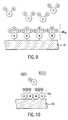
- FIG. 9is a schematic view showing deposition of a first molecule onto a substrate during sequential deposition techniques in accordance with one embodiment of the present invention.
- FIG. 10is a schematic view showing formation of an Al 2 O 3 layer during deposition of second molecule onto a substrate in accordance with one embodiment of the present invention.
- an exemplary wafer processing systemincludes one or more process systems 12 and 14 disposed in a common work area 16 surrounded by a wall 18 .
- Process systems 12 and 14are in data communication with a controller 22 that is connected to one or more monitors, shown as 24 and 26 .
- Monitors 24 and 26typically display common information concerning the process associated with the process systems 12 and 14 .
- Monitor 26is mounted to the wall 18 , with monitor 24 being disposed in the work area 16 .
- Operational control of process systems 12 and 14may be achieved with use of a light pen, associated with one of monitors 24 and 26 , to communicate with controller 22 .
- a light pen 28 ais associated with monitor 24 and facilitates communication with the controller 22 through monitor 24 .
- a light pen 28 bfacilitates communication with controller 22 through monitor 26 .
- each of process systems 12 and 14includes a housing 30 having a base wall 32 , a cover 34 , disposed opposite to the base wall 32 , and a sidewall 35 , extending therebetween.
- Housing 30defines a chamber 36 .
- a pedestal 37is disposed within processing chamber 36 to support a substrate 42 .
- Pedestal 37may be mounted to move between the cover 34 and base wall 32 , using a displacement mechanism (not shown), but is typically fixed proximate to bottom wall 32 .
- Supplies of processing fluids 38 a , 38 b , 38 c , 39 and 40are in fluid communication with the processing chamber 36 via a manifold 34 a .
- Process fluid supply 39consists of a liquid injection assembly having an ampoule 39 a in fluid communication with a vaporizer 39 b .
- Ampoule 39 aincludes a supply of a liquid precursor 39 c and is in fluid communication with supply 38 c , which contains a carrier gas.
- Ampoule 39 ais in fluid communication with vaporizer 39 b via precursor channel 39 d to deliver, to processing chamber 36 , precursor 39 c , with the aid of carrier gas in supply 38 c .
- Ampoule 39 a , liquid 39 c and channel 39 dmay be heated by conventional heating methods, e.g., heating tape (not shown).
- Process fluid supply 40is an ozonator that produces ozone, which is introduced into processing chamber 36 over ozone channel 40 a and is regulated by valve 40 b . Regulation of the flow of gases from supplies 38 a , 38 b , 38 c and 39 is effectuated via flow valves 41 .
- substrate 42may be heated to a desired temperature prior to layer deposition via a heater embedded within pedestal 37 .
- pedestal 37may be resistively heated by applying an electric current from an AC power supply 43 to a heater element 44 .
- Substrate 42is, in turn, heated by pedestal 37 , and can be maintained within a desired process temperature range. The actual temperature, however, is dependent upon the gases employed and the topography of the surface upon which deposition is to occur.
- a temperature sensor 46such as a thermocouple, is also embedded in wafer support pedestal 37 to monitor the temperature of pedestal 37 in a conventional manner.
- the measured temperaturemay be used in a feedback loop to control the electrical current applied to heater element 44 by the power supply 43 , such that the wafer temperature can be maintained or controlled at a desired temperature that is suitable for the particular process application.
- Pedestal 37is optionally heated using radiant heat (not shown).
- a vacuum pump 48is used to evacuate processing chamber 36 and to help maintain the proper gas flows and pressure inside processing chamber 36 .
- an exemplary remote plasma source 49includes a microwave source 49 a , such as a magnetron, coupled via an antenna 49 b to a waveguide system 49 c , and a plasma applicator 49 d .
- plasma applicator 49 dincludes a gas inlet 49 e and an outlet 49 f .
- Gas inlet 49 emay be coupled to a gas source, such as source 49 g via a supply line 49 h having a valve 49 i to control the rate of gas input to gas inlet 49 e from gas source 49 g.
- one of process systems 12 and 14may operate to form, on substrate 42 , a layer of Al 2 O 3 in accordance with the present invention.
- the present inventionis discussed with respect use of Al 2 O 3 as a dielectric layers during the fabrication of memory devices.
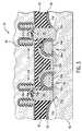
- An exemplary memory deviceincludes a DRAM memory cell 50 shown as being defined between two spaced-apart field oxide regions, FOX, that may be formed on the substrate employing any known technique, such as a LOCOS technique.
- a LOCOS techniqueFormed into substrate 42 between field oxide regions FOX are a plurality of spaced-apart diffusion regions 52 a , 52 b and 52 c .
- Gate structures 53 and 54are disposed between adjacent diffusion regions 52 a , 52 b and 52 c and include a gate electrode 53 a and 54 a with gate dielectric 53 b and 54 b being disposed between gate electrode 53 a and 54 a and substrate 42 .
- each gate electrode 53 a and 54 aDisposed adjacent to each gate electrode 53 a and 54 a is an insulating layer 53 c and 54 c that may be formed from silicon nitride.
- An insulating layer 55is also dispersed adjacent to field oxide regions FOX.
- a pair of storage capacitors 56 and 57are included, each of which is in electrical communication with one of the diffusion regions 52 a and 52 c , respectively.
- a polysilicon plug 58 and 59extends from one of these diffusion regions and connects to storage capacitors 56 and 57 , respectively.
- a conductive layerextends from diffusion region 52 b toward storage capacitors 56 and 57 , forming a bit line electrode 60 .
- a layer 62 of silicon oxideis disposed between storage capacitors 56 and 57 and silicon nitride layers 53 c , 54 c and 55 and bit line electrode 60 .
- each storage capacitor 56 and 57is formed from a pair of spaced-apart polysilicon silicon spacers 56 a and 57 a that are formed with hemispherical grain polysilicon. This increases the surface area of capacitor 56 and 57 due to the rough and bumped surface that results from this layer, effectively increasing the capacitance of the same.
- Blanketing spacers 56 a and 57 ais a dielectric layer 56 b and 57 b .
- a conductive layer 64is disposed adjacent to dielectric layers 56 b and 57 b to complete formation of storage cell capacitors 56 and 57 .
- Conductive layer 64may be formed from virtually any conductive material, such as tungsten titanium-nitride of doped polysilicon.
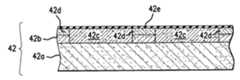
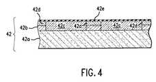
- substrate 42typically includes a wafer 42 a that may be formed from any material suitable for semiconductor processing, such as silicon.
- a wafer 42 amay be formed from any material suitable for semiconductor processing, such as silicon.
- One or more layers, shown as layer 42 bmay be deposited on wafer 42 a .
- Layer 42 bis formed from p-epitaxial silicon that includes doped regions 42 c , separated by shallow trench isolation regions 42 d made employing standard processing techniques.
- Doped regions 42 cmay be either n-type or p-type, depending upon the desired application.
- dielectric layer 42 eFormed adjacent to layer 42 b is dielectric layer 42 e .
- layer 42 eis formed from, Al 2 O 3 , by sequentially exposing substrate 42 to processing gases to chemisorb monolayers of differing compounds onto substrate 42 , discussed more fully below.
- layer 42 eis formed on substrate 42 employing sequential deposition techniques and using an aluminum-containing precursor consisting of AlR m , where R is a ligand and m is an integer, and an oxygen-containing precursor B. Specifically, the initial surface of substrate 42 presents an active ligand to precursor AlR m .
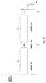
- a carrier gasis introduced into processing chamber 36 during time t 1 before the AlR m is flowed into processing chamber 36 .
- an inert carrier gasis flowed into process chamber 36 during time t 1 , for approximately 5 to 8 seconds.
- the carrier gasis selected from a set of inert gases including Ar, He 2 and N 2 .
- AlR m precursoris introduced into processing chamber 36 to produce a monolayer AlR m on substrate 42 via chemisorption reaction.
- AlR m precursoris introduced into processing chamber 36 along with the carrier gas for approximately 0.8 to 1.5 seconds during time t 2 .
- the flow of the carrier gasterminates, and the flow of the oxygen-containing precursor B is introduced into processing chamber 36 during time t 4 to chemisorb oxygen into the AlR m layer.
- the R ligand present on layer AlR mreacts with precursor B so that oxygen is chemisorbed into layers AlR m .
- the oxygen-containing precursoris introduced into processing chamber 36 for approximately 1 to 3 seconds, during time t 4 . This releases ligands, R, as well as by-products, z, which move away from substrate 42 , thereby concluding one cycle of the sequential deposition technique in accordance with the present invention.
- layer 42 econsists of a mono-molecular layer of Al 2 O 3 .
- the flow of precursor B into processing chamber 36is subsequently terminated.
- a flow of the carrier gasmay be repeated as discussed with respect to t 1 which purges processing chamber 36 of precursor B, ligands, R, and by-products of the chemisorption of oxygen reaction.
- the aforementioned cycles t 2 , t 3 and t 4may be repeated multiple times until Al 2 O 3 layer 42 e reaches a desired thickness.
- subsequent processingmay occur to form, for example, gate dielectric layers 53 b and 54 b of gate structures 53 and 54 using standard deposition techniques.
- the advantage of employing sequential deposition techniques to form gate dielectric layers 53 b and 54 bis that precise control of the gate dielectric thickness and width may be achieved.
- Formation of an Al 2 O 3 layer in this manneris particularly advantageous when creating dielectric layers 56 b and 57 b for storage capacitor 56 and 57 , respectively.
- spaced-apart spacers 56 a and 57 aare covered with hemispherical grain polysilicon, which has a rough, or bumped, surface. Such a surface is very difficult to blanket with a conformal dielectric layer.
- Depositing a conformal layeris further exacerbated by the aspect ratio of the void defined by either spacers 56 a or 57 a and a nadir 56 c and 57 c , respectively.
- the void defined by these featuresmay provide an aspect ratio of as great as 30:1.
- formation of layers 56 b and 57 b by sequential deposition of an Al 2 O 3results in the formation of a highly conformal dielectric layer over spacers 56 a and 57 a.
- crown storage cell capacitor 156An alternate embodiment of the storage capacitors 56 and 57 that may be fabricated in accordance with the present invention is shown in FIG. 8 as crown storage cell capacitor 156 .
- Crown capacitor 156includes a plurality of spaced-apart polysilicon spacers 156 a .
- a serpentine dielectric layer 156 bdisposed adjacent to spacers 156 a , with a conductive layer 164 disposed to blanket dielectric layer 156 b .
- This configurationincreases the surface area of storage capacitor 156 , effectively increasing the capacitance per unit volume of the memory cell.
- Forming dielectric layer 156 b from Al 2 O 3 with the present inventionis advantageous, because of the conformableness of the same.
- dielectric layer 156 bmay be disposed adjacent to spacers 156 a having aspect ratios as high as 30:1, while still providing adequate step coverage.
- precursor AlR mis formed by sublimation of a fluid aluminum-containing compound, Triisopropoxyaluminum, and the oxygen-containing precursor B is selected from a set consisting of ozone and oxygen radicals.
- precursor AlR mis prepared in ampoule 39 a by dissolving Triisopropoxyaluminum a Hexane solution to produce a weight ratio of Triisopropoxyaluminum to Hexane that is between 10:90 to 60:40.
- Triisopropoxyaluminumis beneficial, because it is a nonpyrophoric, resulting in a relative safe compound.
- Triisopropoxyaluminumis a solid making the same difficult to deliver into processing chamber 36 in an efficient manner.
- the use of hexaneis advantageous, because it reduces Triisopropoxyaluminum to provide precursor AlR m with a viscosity that is less than water, i.e., the precursor is a low viscosity fluid.
- low viscosityis defined as a viscosity lower than water.
- the chamber pressureis established to be in a range of 0.1 to 6 Torr, inclusive.
- the substrate temperatureis in the range of 150° C. to 500° C., inclusive.
- the carrier gasis introduced during time t 1 .
- the Triisopropoxyaluminum:Hexane solutionis introduced into the processing chamber 36 , flowing at a flow rate between 1 to 200 mg/min during time t 2 . In this manner, layer AlR m is deposited as a mono-molecular layer of Triisopropoxyaluminum:Hexane by a chemisorption reaction.
- a carrier gasconsisting of Argon, Helium or Nitrogen enters processing chamber 36 during time t 3 to purge the non-deposited Triisopropoxyaluminum:Hexane solution that remains therein, as well as the by-products of the chemisorption reaction.
- oxygen radicals or ozoneis flowed into processing chamber as precursor B.
- the choice of which oxygen-containing precursor to employis dependent upon many factors, including the topology of the underlying layer. For example, oxygen radicals are chemically more reactive than ozone, resulting in a given volume of oxygen radicals reacting more quickly with the aluminum-containing precursor in layer AlR m than the same volume of ozone.
- the relative reactive lifetime of oxygen radicalsis short, compared to ozone, after which time the radicals combine with an adjacent radical forming a less active oxygen molecule.
- ozonemay be preferred for applications requiring formation of an Al 2 O 3 layer on features, such as the roughened topology of spacers 56 a and 57 a having an aspect ratios as great as 30:1, shown in FIG. 3 .
- the oxygen radicalsrecombine before reaching nadir 56 c and 57 c . This has a tendency to create voids and result in other defects in resulting layer 56 b and 57 b .
- the oxygen radicalsbe required to travel long distances over substrate 42 before reacting with the aluminum-containing layer, e.g. 300 mm or larger area glass substrates such as those used for flat-panel displays.
- One manner in which to reduce recombination of oxygen radicalsis to position remote plasma source 49 on cover 34 so as to shorten the distance between remote plasma source 49 and substrate 42 .
- remote plasma source 49may be mounted anywhere desired.
- ozoneovercomes many of the drawbacks of oxygen radical and affords high conformableness with low defects for features having aspect ratios as high as 30:1. This results from the relatively long reactivity life of ozone, compared to that of oxygen radicals. In addition, ozone is quite useful when having to travel long distances over substrate 42 before reacting with layer AlR m .
- oxygen radicals employed as the oxygen-containing precursorit may be activated by remote plasma source 49 .
- oxygen gas from supply 49 gwould be flowed into applicator 49 d .
- Microwave source 49 awould generate microwave energy at power levels between 100W and 3000W. The microwave energy would propagate through waveguide 49 c and into applicator 49 d , dissociating oxygen molecules into a plurality of reactive radicals.
- the reactive radicalswould flow through outlet 49 f and into processing chamber 36 .
- the oxygen radicals or ionsreact with the Triisopropoxyaluminum:Hexane monolayer 42 e to form a monolayer of Al 2 O 3 .
- ozoneemployed as the oxygen-containing precursor, ozone would be introduced into processing chamber 36 at a rate of 300-3000 sccm.
- An alternate precursor chemistry for sequential deposition of Al 2 O 3 films in accordance with the present inventionincludes a liquid aluminum-containing precursor consisting of a Triisopropoxyaluminum and Tetrahydrofuran solution prepared in ampoule 39 a at a weight ratio of Triisopropoxyaluminum to Tetrahydrofuran that is between 10:90 to 60:40 to form a low viscosity aluminum-containing precursor.
- the oxygen-containing precursoris selected from a set consisting of ozone and oxygen radicals, the choice of which is based upon, inter alia, the topology of substrate 42 .
- Tetrahydrofuranis advantageous, because it reduces Triisopropoxyaluminum to a fluid to provide precursor AlR m with a viscosity that is less than water. As discussed above, this reduces the time required to deposit an aluminum-containing layer.
- the chamber pressureis established to be in a range of 0.1 to 6 Torr, inclusive.
- the substrate temperatureis in the range of 150° C. to 300° C., inclusive.
- the carrier gasis introduced during time t 1 .
- the Triisopropoxyaluminum:Tetrahydrofuran solutionis introduced into the processing chamber 36 , flowing at a flow rate between 1 to 200 mg/min during time t 2 . In this manner, a monolayer of Triisopropoxyaluminum:Tetrahydrofuran is deposited on substrate 42 by a chemisorption reaction.
- a carrier gasconsisting of Argon, Helium or Nitrogen enters processing chamber 36 during time t 3 to purge the non-deposited Triisopropoxyaluminum:Tetrahydrofuran solution that remains therein, as well as the by-products of the chemisorption reaction.
- a carrier gasconsisting of Argon, Helium or Nitrogen enters processing chamber 36 during time t 3 to purge the non-deposited Triisopropoxyaluminum:Tetrahydrofuran solution that remains therein, as well as the by-products of the chemisorption reaction.
- an oxygen-containing precursorozone would be introduced into processing chamber 36 at a rate of 300-3000 sccm.
- oxygen radicals employed as the oxygen-containing precursoroxygen gas would be flowed into applicator 49 d of remote plasma source 49 .
- Microwave source 49 awould generate microwave energy at power levels between 100W and 3000W.
- the microwave energywould propagate through waveguide 49 c and into applicator 49 c , dissociating oxygen molecules into a plurality of reactive radicals.
- the reactive radicalswould flow through outlet 49 f and into processing chamber 36 .
- the oxygen radicals or ionsreact with the Triisopropoxyaluminum:Tetrahydrofuran monolayer present on substrate 42 to chemisorb oxygen into the monolayer.
- an ALD cycleis complete and a surface comprising a monolayer of Al 2 O 3 remains upon substrate 42 .
- Additional alternate precursor chemistries for sequential deposition of Al 2 O 3 films in accordance with the present inventioninclude a liquid aluminum-containing precursor consisting of a solution of Dimethylaluminumhydride and dimethylethylamine, or a solution of Ethylpiperidine and Dimethylaluminumhydride.
- Dimethylaluminumhydrideis pyrophoric, but was found to be easily converted to a nonpyrophoric low viscosity fluid by mixing with either Dimethylethylamine or Ethylpiperidine.
- Dimethylaluminumhydrideis mixed in ampoule 39 a at a weight ratio between 10:90 to 60:40 of Dimethylaluminumhydride to either Dimethylethylamine or Ethylpiperidine.
- the oxygen-containing precursoris selected from a set consisting of ozone and oxygen radicals, the choice being dependent upon, inter alia, substrate 42 topology, as discussed above.
- the chamber pressureis established to be in a range of 0.1 to 4 Torr, inclusive.
- the substrate temperatureis in the range of 100° C. to 300° C., inclusive.
- the carrier gasis introduced during time t 1 .
- the Dimethylaluminumhydride:dimethylethylamine or Ethylpiperidine:Dimethylaluminumhydride solutionis introduced into the processing chamber 36 , flowing at a flow rate between 1 to 200 mg/min during time t 2 . In this manner, a monolayer of either Dimethylaluminumhydride:Dimethylethylamine or Ethylpiperidine:Dimethylaluminumhydride is deposited on substrate 42 by a chemisorption reaction.
- a carrier gasconsisting of Argon, Helium or Nitrogen enters processing chamber 36 during time t 3 to purge the non-deposited Dimethylaluminumhydride:Dimethylethylamine or Ethylpiperidine:Dimethylaluminumhydride solution that remains therein, as well as the by-products of the chemisorption reaction.
- a carrier gasconsisting of Argon, Helium or Nitrogen enters processing chamber 36 during time t 3 to purge the non-deposited Dimethylaluminumhydride:Dimethylethylamine or Ethylpiperidine:Dimethylaluminumhydride solution that remains therein, as well as the by-products of the chemisorption reaction.
- ozoneemployed as the oxygen-containing precursor, ozone would be introduced into processing chamber 36 at a rate of 300-3000 sccm.
- oxygen gaswould be flowed into applicator 49 d of remote plasma source 49 .
- Microwave source 49 awould generate microwave energy at power levels between 100W and 3000W.
- the microwave energywould propagate through waveguide 49 c and into applicator 49 c , dissociating oxygen molecules into a plurality of reactive radicals.
- the reactive radicalswould flow through outlet 49 f and into processing chamber 36 .
- the oxygen in the oxygen-precursorreacts with the monolayer present of substrate 42 to chemisorb oxygen therein.
- an ALD cycleis complete and a surface comprising a monolayer of Al 2 O 3 remains upon substrate 42 .
- an inexpensive oxygen-containing precursor, Bb yis substituted for precursor B, discussed above with respect to FIGS. 5, 6 and 7 .
- the oxygen precursor Bb yconsists of H 2 O, shown more clearly in FIG. 8 .
- aluminum-containing precursor AlR mconsists of solid AlCl 3 that is contained in ampoule 39 a .
- the chamber pressureis established to be in a range of 0.1 to 500 Torr, inclusive.
- the substrate temperatureis in the range of 100° C. to 300° C., inclusive.
- the ampoule 39 ais heated to approximately 190° C., vaporizing the AlCl 3 to form a low viscosity fluid.
- the carrier gasis introduced during time t 1 .
- the AlCl 3 precursoris introduced into processing chamber 36 , flowing at a flow rate between 20-1000 sccm during time t 2 .
- the initial surface of substrate 42presents an active ligand to the AlCl 3 precursor, resulting in layer AlR m consisting of AlCl 3 , with the Cl 3 exposed to the processing chamber 36 .
- a carrier gasconsisting of Argon, Helium or Nitrogen enters processing chamber 36 during time t 3 to purge the non-deposited AlCl 3 precursor that remains therein and by-products of the chemisorption reaction. This is followed by termination of the flow of the carrier gas and introduction of the oxygen-containing precursor at time t 4 .
- vaporized H 2 Ois introduced into processing chamber 36 at a rate of 300-3000 sccm.
- the vaporized H 2 Omay be introduced as steam through a steam line (not shown).
- the AlCl 3reacts with the H 2 O, releasing HCL and Cl 2 molecules that move away from substrate 42 and are subsequently pumped from processing chamber 36 , leaving a monolayer of Al 2 O 3 .
- oxygen contained in the water vaporreacts with the AlCl 3 monolayer, disposed on substrate 42 , to chemisorb oxygen therein.
- a sequential deposition cycleis complete and a surface comprising monolayer 42 e of Al 2 O 3 remains upon substrate 42 .
- the processproceeds cycle after cycle, until the desired thickness is achieved.
- Wateris also employed as the oxygen-containing precursor Bb y in conjunction with either of the solutions of Dimethylaluminumhydride and Dimethylethylamine, or of Ethylpiperidine and Dimethylaluminumhydride, which are prepared as discussed above. To that end, the process conditions mentioned above are employed, with water vapor being flowed into processing chamber 36 , in place of either oxygen radicals or ozone and at a rate of 2000 sccm.
- the afore-described processes for depositing the Al 2 O 3 layer 42 emay be controlled using a computer program product that is executed by the controller 22 .
- the controller 22includes a central processing unit (CPU) 70 , a volatile memory, such as a random access memory (RAM) 72 and permanent storage media, such as a floppy disk drive for use with a floppy diskette, or hard disk drive 74 .
- the computer program codecan be written in any conventional computer readable programming language; for example, 68000 assembly language, C, C++, Pascal, Fortran, and the like.
- Suitable program codeis entered into a single file, or multiple files, using a conventional text editor and stored or embodied in a computer-readable medium, such as the hard disk drive 74 . If the entered code text is in a high level language, the code is compiled and the resultant compiler code is then linked with an object code of precompiled Windows® library routines. To execute the linked and compiled object code the system user invokes the object code, causing the CPU 70 to load the code in RAM 72 . The CPU 70 then reads and executes the code to perform the tasks identified in the program.
- sequential deposition processmay have a different initial sequence.
- the initial sequencemay include exposing the substrate the oxygen-containing precursor before the aluminum-containing precursor is introduced into the processing chamber. Additionally, removal of precursors and by-products from the processing chamber may occur by concurrently pumping the processing chamber and flowing a carrier gas therein. In this manner, temperature and pressure fluctuations may be minimized.
- the oxygen precursorhas been discussed with respect to the oxygen radical-ozone molecule dichotomy.
Landscapes
- Chemical & Material Sciences (AREA)
- Engineering & Computer Science (AREA)
- Mechanical Engineering (AREA)
- General Chemical & Material Sciences (AREA)
- Organic Chemistry (AREA)
- Metallurgy (AREA)
- Materials Engineering (AREA)
- Chemical Kinetics & Catalysis (AREA)
- Microelectronics & Electronic Packaging (AREA)
- Condensed Matter Physics & Semiconductors (AREA)
- Power Engineering (AREA)
- General Physics & Mathematics (AREA)
- Physics & Mathematics (AREA)
- Computer Hardware Design (AREA)
- Manufacturing & Machinery (AREA)
- Inorganic Chemistry (AREA)
- Formation Of Insulating Films (AREA)
- Chemical Vapour Deposition (AREA)
Abstract
Description
1. Field of the Invention
This invention relates to semiconductor processing. More particularly, this invention relates to a method of sequential deposition of high-K Al2O3films on a substrate.
2. Description of the Related Art
The semiconductor industry continues to strive for larger production yields while increasing the uniformity of layers deposited on substrates having increasingly larger surface areas. These same factors in combination with new materials also provide higher integration of circuits per unit area of the substrate. High-K dielectrics are an example of new materials currently investigated. These materials are being investigated as a potential replacement for SiO2as both gate and DRAM dielectrics. The present and future requirements for SiO2in MOS structures relate to thicknesses<5 nm. The equivalent thicknesses may be achieved with higher K materials physically thicker than the SiO2layers. The choice of suitable high-K dielectrics is typically directed to materials with relatively large band gaps and high dielectric constants. The band gap of Al2O3is 9 eV, which is considerably larger than that of most high-K materials and comparable to that of SiO2. Also, the dielectric constant of Al2O3is 9, which is more than two times greater than that of SiO2. Therefore, Al2O3is a suitable high-K replacement for SiO2.
As circuit integration increases, the need for greater uniformity and process control regarding layer thickness rises. As a result, various technologies have been developed to deposit layers on substrates in a cost-effective manner, while maintaining control over the characteristics of the layer. Chemical Vapor Deposition (CVD) is a common deposition process employed for depositing layers on a substrate. CVD is a flux-dependent deposition technique that requires precise control of the substrate temperature and precursors introduced into the processing chamber in order to produce a desired layer of uniform thickness. These requirements become more critical as substrate size increases, creating a need for more complexity in chamber design and fluid flow technique to maintain adequate uniformity.
Another deposition process that demonstrates superior step coverage is a sequential deposition technique known as Atomic Layer Deposition (ALD). ALD has steps of chemisorption that deposit monolayers of reactive precursor molecules on a substrate surface. A drawback with ALD of Al2O3films is that the deposition rate is much lower than conventional CVD methodologies, in part, because many of the precursors employed are highly viscous or solid. This increases the time required to introduce the precursors into a processing chamber and, thus, processing time.
Thus, a need exists, to provide an improved technique to form Al2O3films employing sequential deposition techniques, such as Atomic Layer Deposition.
Disclosed is a method and apparatus for depositing high-K Al2O3films on a substrate disposed in a processing chamber employing liquid precursors having low viscosity. In this manner, the time required to form an Al2O3film using ALD techniques is reduced. The method features sequential flow of aluminum and oxygen precursors into the processing chamber. To that end, the aluminum precursor is chemisorbed onto the wafer surface when it flows into the processing chamber. The non-chemisorbed aluminum precursor is then purged from the processing chamber, followed by introduction of the oxygen precursor. The oxygen precursor reacts with the chemisorbed layer, creating a monolayer of Al2O3. Finally, excess oxygen precursor and by-products of the reaction are purged from the processing chamber completing an ALD cycle. To obtain the desired film thickness, multiple ALD cycles are repeated. The apparatus includes features that carryout the steps of the method.
FIG. 1 is a perspective view of a semiconductor processing system in accordance with the present invention;
FIG. 2 is a detailed view of processing chambers shown above in FIG. 1;
FIG. 3 is a detailed cross-sectional view of a memory cell formed on a substrate shown in FIG. 2;
FIG. 4 is a detailed cross-sectional view of the substrate shown in FIG. 3 during formation of a dielectric layer that will eventually become a gate dielectric layer for transistors associated with the memory cell shown in FIG. 3;
FIG. 5 is a schematic view showing deposition of a first molecule onto a substrate using sequential deposition techniques in accordance with one embodiment of the present invention;
FIG. 6 is a schematic view showing formation of an Al2O3layer during deposition of second molecule onto a substrate in accordance with one embodiment of the present invention;
FIG. 7 is a graphical representation showing the concentration of gases introduced into the processing chamber shown in FIG. 2, and the time in which the gases are present in the processing chamber to deposit the Al2O3layer shown above in FIG. 4, in accordance with one embodiment of the present invention;
FIG. 8 is a detailed cross-sectional view of an alternate embodiment of a storage capacitor shown in FIG. 3;
FIG. 9 is a schematic view showing deposition of a first molecule onto a substrate during sequential deposition techniques in accordance with one embodiment of the present invention; and
FIG. 10 is a schematic view showing formation of an Al2O3layer during deposition of second molecule onto a substrate in accordance with one embodiment of the present invention.
Referring to FIG. 1, an exemplary wafer processing system includes one ormore process systems common work area 16 surrounded by awall 18.Process systems controller 22 that is connected to one or more monitors, shown as24 and26.Monitors process systems Monitor 26 is mounted to thewall 18, withmonitor 24 being disposed in thework area 16. Operational control ofprocess systems monitors controller 22. For example, alight pen 28ais associated withmonitor 24 and facilitates communication with thecontroller 22 throughmonitor 24. Alight pen 28bfacilitates communication withcontroller 22 throughmonitor 26.
Referring to both FIGS. 1 and 2, each ofprocess systems housing 30 having abase wall 32, acover 34, disposed opposite to thebase wall 32, and asidewall 35, extending therebetween.Housing 30 defines achamber 36. Apedestal 37 is disposed withinprocessing chamber 36 to support asubstrate 42.Pedestal 37 may be mounted to move between thecover 34 andbase wall 32, using a displacement mechanism (not shown), but is typically fixed proximate tobottom wall 32. Supplies ofprocessing fluids processing chamber 36 via a manifold34a.Process fluid supply 39 consists of a liquid injection assembly having an ampoule39ain fluid communication with avaporizer 39b. Ampoule39aincludes a supply of aliquid precursor 39cand is in fluid communication withsupply 38c, which contains a carrier gas. Ampoule39ais in fluid communication withvaporizer 39bviaprecursor channel 39dto deliver, to processingchamber 36,precursor 39c, with the aid of carrier gas insupply 38c. Ampoule39a,liquid 39candchannel 39dmay be heated by conventional heating methods, e.g., heating tape (not shown).Process fluid supply 40 is an ozonator that produces ozone, which is introduced intoprocessing chamber 36 overozone channel 40aand is regulated byvalve 40b. Regulation of the flow of gases fromsupplies flow valves 41.
Depending on the specific process,substrate 42 may be heated to a desired temperature prior to layer deposition via a heater embedded withinpedestal 37. For example,pedestal 37 may be resistively heated by applying an electric current from anAC power supply 43 to aheater element 44.Substrate 42 is, in turn, heated bypedestal 37, and can be maintained within a desired process temperature range. The actual temperature, however, is dependent upon the gases employed and the topography of the surface upon which deposition is to occur. Atemperature sensor 46, such as a thermocouple, is also embedded inwafer support pedestal 37 to monitor the temperature ofpedestal 37 in a conventional manner. For example, the measured temperature may be used in a feedback loop to control the electrical current applied toheater element 44 by thepower supply 43, such that the wafer temperature can be maintained or controlled at a desired temperature that is suitable for the particular process application.Pedestal 37 is optionally heated using radiant heat (not shown). Avacuum pump 48 is used to evacuateprocessing chamber 36 and to help maintain the proper gas flows and pressure inside processingchamber 36.
Referring to both FIGS. 1 and 2, for processes requiring a plasma, one or more ofprocess systems remote plasma source 49. Although virtually any remote plasma source may be included, an exemplaryremote plasma source 49 includes amicrowave source 49a, such as a magnetron, coupled via anantenna 49bto awaveguide system 49c, and aplasma applicator 49d. Defining a volume therein,plasma applicator 49dincludes agas inlet 49eand anoutlet 49f.Gas inlet 49emay be coupled to a gas source, such assource 49gvia asupply line 49hhaving avalve 49ito control the rate of gas input togas inlet 49efromgas source 49g.
Referring to FIGS. 1 and 3, one ofprocess systems substrate 42, a layer of Al2O3in accordance with the present invention. For exemplary purposes, the present invention is discussed with respect use of Al2O3as a dielectric layers during the fabrication of memory devices.
An exemplary memory device includes aDRAM memory cell 50 shown as being defined between two spaced-apart field oxide regions, FOX, that may be formed on the substrate employing any known technique, such as a LOCOS technique. Formed intosubstrate 42 between field oxide regions FOX are a plurality of spaced-apartdiffusion regions Gate structures adjacent diffusion regions gate electrode 53aand54awith gate dielectric53band54bbeing disposed betweengate electrode 53aand54aandsubstrate 42. Disposed adjacent to eachgate electrode 53aand54ais an insulatinglayer layer 55 is also dispersed adjacent to field oxide regions FOX. A pair ofstorage capacitors diffusion regions polysilicon plug storage capacitors diffusion region 52btowardstorage capacitors bit line electrode 60. Alayer 62 of silicon oxide is disposed betweenstorage capacitors bit line electrode 60.
As shown, eachstorage capacitor polysilicon silicon spacers 56aand57athat are formed with hemispherical grain polysilicon. This increases the surface area ofcapacitor spacers 56aand57ais adielectric layer conductive layer 64 is disposed adjacent todielectric layers storage cell capacitors Conductive layer 64 may be formed from virtually any conductive material, such as tungsten titanium-nitride of doped polysilicon.
Referring to both FIGS. 3 and 4, with respect to formation of gate dielectric53band54b,substrate 42 typically includes awafer 42athat may be formed from any material suitable for semiconductor processing, such as silicon. One or more layers, shown aslayer 42b, may be deposited onwafer 42a.Layer 42bis formed from p-epitaxial silicon that includes dopedregions 42c, separated by shallowtrench isolation regions 42dmade employing standard processing techniques.Doped regions 42cmay be either n-type or p-type, depending upon the desired application.
Formed adjacent to layer42bisdielectric layer 42e. In the present example,layer 42eis formed from, Al2O3, by sequentially exposingsubstrate 42 to processing gases to chemisorb monolayers of differing compounds ontosubstrate 42, discussed more fully below.
Referring to FIGS.2 and5-7, in thepresent example layer 42eis formed onsubstrate 42 employing sequential deposition techniques and using an aluminum-containing precursor consisting of AlRm, where R is a ligand and m is an integer, and an oxygen-containing precursor B. Specifically, the initial surface ofsubstrate 42 presents an active ligand to precursor AlRm.
Once the processing pressure and deposition temperature have been established, a carrier gas is introduced intoprocessing chamber 36 during time t1before the AlRmis flowed intoprocessing chamber 36. Specifically, an inert carrier gas is flowed intoprocess chamber 36 during time t1, for approximately 5 to 8 seconds. The carrier gas is selected from a set of inert gases including Ar, He2and N2. During time t2, AlRmprecursor is introduced intoprocessing chamber 36 to produce a monolayer AlRmonsubstrate 42 via chemisorption reaction. Typically, AlRmprecursor is introduced intoprocessing chamber 36 along with the carrier gas for approximately 0.8 to 1.5 seconds during time t2. After t2has lapsed, the flow of AlRmprocess gas terminates, and the flow of the carrier gas continues during time t3, purgingprocessing chamber 36 of AlRmprecursor and by-products of the chemisorption reaction. This lasts for approximately 5 to 8 seconds.
After t3has lapsed, the flow of the carrier gas terminates, and the flow of the oxygen-containing precursor B is introduced intoprocessing chamber 36 during time t4to chemisorb oxygen into the AlRmlayer. Specifically, the R ligand present on layer AlRmreacts with precursor B so that oxygen is chemisorbed into layers AlRm. To that end, the oxygen-containing precursor is introduced intoprocessing chamber 36 for approximately 1 to 3 seconds, during time t4. This releases ligands, R, as well as by-products, z, which move away fromsubstrate 42, thereby concluding one cycle of the sequential deposition technique in accordance with the present invention. In thismanner layer 42econsists of a mono-molecular layer of Al2O3.
The flow of precursor B intoprocessing chamber 36 is subsequently terminated. After the flow of precursor B terminates, a flow of the carrier gas may be repeated as discussed with respect to t1which purgesprocessing chamber 36 of precursor B, ligands, R, and by-products of the chemisorption of oxygen reaction. The aforementioned cycles t2, t3and t4may be repeated multiple times until Al2O3layer42ereaches a desired thickness. After Al2O3layer42ereaches a desired thickness, subsequent processing may occur to form, for example, gate dielectric layers53band54bofgate structures
Formation of an Al2O3layer in this manner is particularly advantageous when creatingdielectric layers storage capacitor apart spacers 56aand57aare covered with hemispherical grain polysilicon, which has a rough, or bumped, surface. Such a surface is very difficult to blanket with a conformal dielectric layer. Depositing a conformal layer is further exacerbated by the aspect ratio of the void defined by eitherspacers 56aor57aand anadir 56cand57c, respectively. The void defined by these features may provide an aspect ratio of as great as 30:1. However, formation oflayers spacers 56aand57a.
An alternate embodiment of thestorage capacitors storage cell capacitor 156.Crown capacitor 156 includes a plurality of spaced-apartpolysilicon spacers 156a. Aserpentine dielectric layer 156bdisposed adjacent to spacers156a, with aconductive layer 164 disposed toblanket dielectric layer 156b. This configuration increases the surface area ofstorage capacitor 156, effectively increasing the capacitance per unit volume of the memory cell. Formingdielectric layer 156bfrom Al2O3with the present invention is advantageous, because of the conformableness of the same. As a resultdielectric layer 156bmay be disposed adjacent to spacers156ahaving aspect ratios as high as 30:1, while still providing adequate step coverage.
Referring to FIGS. 2,4 and7, one example of precursor AlRmis formed by sublimation of a fluid aluminum-containing compound, Triisopropoxyaluminum, and the oxygen-containing precursor B is selected from a set consisting of ozone and oxygen radicals. To that end, precursor AlRmis prepared in ampoule39aby dissolving Triisopropoxyaluminum a Hexane solution to produce a weight ratio of Triisopropoxyaluminum to Hexane that is between 10:90 to 60:40. The use of Triisopropoxyaluminum is beneficial, because it is a nonpyrophoric, resulting in a relative safe compound. However, Triisopropoxyaluminum is a solid making the same difficult to deliver intoprocessing chamber 36 in an efficient manner. The use of hexane is advantageous, because it reduces Triisopropoxyaluminum to provide precursor AlRmwith a viscosity that is less than water, i.e., the precursor is a low viscosity fluid. For purposes of the present invention, low viscosity is defined as a viscosity lower than water. By providing precursor AlRmwith low viscosity,injection system 39 may more rapidly inject precursor AlRmintoprocessing chamber 36, thereby reducing the time required to formlayer 42e.
The chamber pressure is established to be in a range of 0.1 to 6 Torr, inclusive. The substrate temperature is in the range of 150° C. to 500° C., inclusive. Once the processing pressure and deposition temperature have been reached, the carrier gas is introduced during time t1. The Triisopropoxyaluminum:Hexane solution is introduced into theprocessing chamber 36, flowing at a flow rate between 1 to 200 mg/min during time t2. In this manner, layer AlRmis deposited as a mono-molecular layer of Triisopropoxyaluminum:Hexane by a chemisorption reaction. Thereafter, a carrier gas consisting of Argon, Helium or Nitrogen entersprocessing chamber 36 during time t3to purge the non-deposited Triisopropoxyaluminum:Hexane solution that remains therein, as well as the by-products of the chemisorption reaction.
During time t4, either oxygen radicals or ozone is flowed into processing chamber as precursor B. The choice of which oxygen-containing precursor to employ is dependent upon many factors, including the topology of the underlying layer. For example, oxygen radicals are chemically more reactive than ozone, resulting in a given volume of oxygen radicals reacting more quickly with the aluminum-containing precursor in layer AlRmthan the same volume of ozone. However, the relative reactive lifetime of oxygen radicals is short, compared to ozone, after which time the radicals combine with an adjacent radical forming a less active oxygen molecule. As a result, ozone may be preferred for applications requiring formation of an Al2O3layer on features, such as the roughened topology ofspacers 56aand57ahaving an aspect ratios as great as 30:1, shown in FIG.3. Often, the oxygen radicals recombine before reachingnadir 56cand57c. This has a tendency to create voids and result in other defects in resultinglayer substrate 42 before reacting with the aluminum-containing layer, e.g. 300 mm or larger area glass substrates such as those used for flat-panel displays. One manner in which to reduce recombination of oxygen radicals is to positionremote plasma source 49 oncover 34 so as to shorten the distance betweenremote plasma source 49 andsubstrate 42. However, it should be understood thatremote plasma source 49 may be mounted anywhere desired.
Referring to both FIGS. 3 and 4, ozone overcomes many of the drawbacks of oxygen radical and affords high conformableness with low defects for features having aspect ratios as high as 30:1. This results from the relatively long reactivity life of ozone, compared to that of oxygen radicals. In addition, ozone is quite useful when having to travel long distances oversubstrate 42 before reacting with layer AlRm.
Referring to FIGS. 2,4 and7 were oxygen radicals employed as the oxygen-containing precursor, it may be activated byremote plasma source 49. To that end, oxygen gas fromsupply 49gwould be flowed intoapplicator 49d.Microwave source 49awould generate microwave energy at power levels between 100W and 3000W. The microwave energy would propagate throughwaveguide 49cand intoapplicator 49d, dissociating oxygen molecules into a plurality of reactive radicals. The reactive radicals would flow throughoutlet 49fand intoprocessing chamber 36. In this manner, the oxygen radicals or ions react with the Triisopropoxyaluminum:Hexane monolayer 42eto form a monolayer of Al2O3. At this point, an ALD cycle is complete and a surface comprising a monolayer of Al2O3remains uponsubstrate 42. Were ozone employed as the oxygen-containing precursor, ozone would be introduced intoprocessing chamber 36 at a rate of 300-3000 sccm.
An alternate precursor chemistry for sequential deposition of Al2O3films in accordance with the present invention includes a liquid aluminum-containing precursor consisting of a Triisopropoxyaluminum and Tetrahydrofuran solution prepared in ampoule39aat a weight ratio of Triisopropoxyaluminum to Tetrahydrofuran that is between 10:90 to 60:40 to form a low viscosity aluminum-containing precursor. As before, the oxygen-containing precursor is selected from a set consisting of ozone and oxygen radicals, the choice of which is based upon, inter alia, the topology ofsubstrate 42. The use of Tetrahydrofuran is advantageous, because it reduces Triisopropoxyaluminum to a fluid to provide precursor AlRmwith a viscosity that is less than water. As discussed above, this reduces the time required to deposit an aluminum-containing layer.
The chamber pressure is established to be in a range of 0.1 to 6 Torr, inclusive. The substrate temperature is in the range of 150° C. to 300° C., inclusive. Once the processing pressure and deposition temperature have been reached, the carrier gas is introduced during time t1. The Triisopropoxyaluminum:Tetrahydrofuran solution is introduced into theprocessing chamber 36, flowing at a flow rate between 1 to 200 mg/min during time t2. In this manner, a monolayer of Triisopropoxyaluminum:Tetrahydrofuran is deposited onsubstrate 42 by a chemisorption reaction. Thereafter, a carrier gas consisting of Argon, Helium or Nitrogen entersprocessing chamber 36 during time t3to purge the non-deposited Triisopropoxyaluminum:Tetrahydrofuran solution that remains therein, as well as the by-products of the chemisorption reaction. This is followed by termination of the flow of the carrier gas and introduction of an oxygen-containing precursor during time t4. Were ozone employed as the oxygen-containing precursor, ozone would be introduced intoprocessing chamber 36 at a rate of 300-3000 sccm.
Were oxygen radicals employed as the oxygen-containing precursor, then oxygen gas would be flowed intoapplicator 49dofremote plasma source 49.Microwave source 49awould generate microwave energy at power levels between 100W and 3000W. The microwave energy would propagate throughwaveguide 49cand intoapplicator 49c, dissociating oxygen molecules into a plurality of reactive radicals. The reactive radicals would flow throughoutlet 49fand intoprocessing chamber 36. In this manner, the oxygen radicals or ions react with the Triisopropoxyaluminum:Tetrahydrofuran monolayer present onsubstrate 42 to chemisorb oxygen into the monolayer. At this point, an ALD cycle is complete and a surface comprising a monolayer of Al2O3remains uponsubstrate 42.
Additional alternate precursor chemistries for sequential deposition of Al2O3films in accordance with the present invention include a liquid aluminum-containing precursor consisting of a solution of Dimethylaluminumhydride and dimethylethylamine, or a solution of Ethylpiperidine and Dimethylaluminumhydride. Unlike Triisopropoxyaluminum, Dimethylaluminumhydride is pyrophoric, but was found to be easily converted to a nonpyrophoric low viscosity fluid by mixing with either Dimethylethylamine or Ethylpiperidine. To that end, Dimethylaluminumhydride is mixed in ampoule39aat a weight ratio between 10:90 to 60:40 of Dimethylaluminumhydride to either Dimethylethylamine or Ethylpiperidine. The oxygen-containing precursor is selected from a set consisting of ozone and oxygen radicals, the choice being dependent upon, inter alia,substrate 42 topology, as discussed above.
The chamber pressure is established to be in a range of 0.1 to 4 Torr, inclusive. The substrate temperature is in the range of 100° C. to 300° C., inclusive. Once the processing pressure and deposition temperature have been reached, the carrier gas is introduced during time t1. The Dimethylaluminumhydride:dimethylethylamine or Ethylpiperidine:Dimethylaluminumhydride solution is introduced into theprocessing chamber 36, flowing at a flow rate between 1 to 200 mg/min during time t2. In this manner, a monolayer of either Dimethylaluminumhydride:Dimethylethylamine or Ethylpiperidine:Dimethylaluminumhydride is deposited onsubstrate 42 by a chemisorption reaction. Thereafter, a carrier gas consisting of Argon, Helium or Nitrogen entersprocessing chamber 36 during time t3to purge the non-deposited Dimethylaluminumhydride:Dimethylethylamine or Ethylpiperidine:Dimethylaluminumhydride solution that remains therein, as well as the by-products of the chemisorption reaction. This is followed by termination of the flow of the inert gas and introduction of an oxygen-containing precursor during time t4. Were ozone employed as the oxygen-containing precursor, ozone would be introduced intoprocessing chamber 36 at a rate of 300-3000 sccm.
Were oxygen radicals employed as the oxygen-containing precursor, then oxygen gas would be flowed intoapplicator 49dofremote plasma source 49.Microwave source 49awould generate microwave energy at power levels between 100W and 3000W. The microwave energy would propagate throughwaveguide 49cand intoapplicator 49c, dissociating oxygen molecules into a plurality of reactive radicals. The reactive radicals would flow throughoutlet 49fand intoprocessing chamber 36. In this manner, the oxygen in the oxygen-precursor reacts with the monolayer present ofsubstrate 42 to chemisorb oxygen therein. At this point, an ALD cycle is complete and a surface comprising a monolayer of Al2O3remains uponsubstrate 42.
In yet another embodiment of the present invention, an inexpensive oxygen-containing precursor, Bby, is substituted for precursor B, discussed above with respect to FIGS. 5,6 and7. The oxygen precursor Bbyconsists of H2O, shown more clearly in FIG.8.
Referring to FIGS.2 and7-9, aluminum-containing precursor AlRmconsists of solid AlCl3that is contained in ampoule39a. The chamber pressure is established to be in a range of 0.1 to 500 Torr, inclusive. The substrate temperature is in the range of 100° C. to 300° C., inclusive. Taking advantage of the low sublimation temperature of AlCl3, the ampoule39ais heated to approximately 190° C., vaporizing the AlCl3to form a low viscosity fluid. Once the processing pressure and deposition temperature have been reached, the carrier gas is introduced during time t1. The AlCl3precursor is introduced intoprocessing chamber 36, flowing at a flow rate between 20-1000 sccm during time t2.
As discussed above, the initial surface ofsubstrate 42 presents an active ligand to the AlCl3precursor, resulting in layer AlRmconsisting of AlCl3, with the Cl3exposed to theprocessing chamber 36. Thereafter, a carrier gas consisting of Argon, Helium or Nitrogen entersprocessing chamber 36 during time t3to purge the non-deposited AlCl3precursor that remains therein and by-products of the chemisorption reaction. This is followed by termination of the flow of the carrier gas and introduction of the oxygen-containing precursor at time t4. During time t4, vaporized H2O is introduced intoprocessing chamber 36 at a rate of 300-3000 sccm. The vaporized H2O may be introduced as steam through a steam line (not shown). The AlCl3reacts with the H2O, releasing HCL and Cl2molecules that move away fromsubstrate 42 and are subsequently pumped from processingchamber 36, leaving a monolayer of Al2O3. Specifically, oxygen contained in the water vapor reacts with the AlCl3monolayer, disposed onsubstrate 42, to chemisorb oxygen therein. At this point, a sequential deposition cycle is complete and asurface comprising monolayer 42eof Al2O3remains uponsubstrate 42. The process proceeds cycle after cycle, until the desired thickness is achieved.
Water is also employed as the oxygen-containing precursor Bbyin conjunction with either of the solutions of Dimethylaluminumhydride and Dimethylethylamine, or of Ethylpiperidine and Dimethylaluminumhydride, which are prepared as discussed above. To that end, the process conditions mentioned above are employed, with water vapor being flowed intoprocessing chamber 36, in place of either oxygen radicals or ozone and at a rate of 2000 sccm.
Referring to FIGS. 2 and 4, the afore-described processes for depositing the Al2O3layer42emay be controlled using a computer program product that is executed by thecontroller 22. To that end, thecontroller 22 includes a central processing unit (CPU)70, a volatile memory, such as a random access memory (RAM)72 and permanent storage media, such as a floppy disk drive for use with a floppy diskette, orhard disk drive 74. The computer program code can be written in any conventional computer readable programming language; for example, 68000 assembly language, C, C++, Pascal, Fortran, and the like. Suitable program code is entered into a single file, or multiple files, using a conventional text editor and stored or embodied in a computer-readable medium, such as thehard disk drive 74. If the entered code text is in a high level language, the code is compiled and the resultant compiler code is then linked with an object code of precompiled Windows® library routines. To execute the linked and compiled object code the system user invokes the object code, causing theCPU 70 to load the code inRAM 72. TheCPU 70 then reads and executes the code to perform the tasks identified in the program.
Although the invention has been described in terms of specific embodiments, one skilled in the art will recognize that various changes to the reaction conditions, i.e., temperature, pressure, film thickness and the like can be substituted and are meant to be included herein and sequence of gases being deposited. For example, sequential deposition process may have a different initial sequence. The initial sequence may include exposing the substrate the oxygen-containing precursor before the aluminum-containing precursor is introduced into the processing chamber. Additionally, removal of precursors and by-products from the processing chamber may occur by concurrently pumping the processing chamber and flowing a carrier gas therein. In this manner, temperature and pressure fluctuations may be minimized. Further, the oxygen precursor has been discussed with respect to the oxygen radical-ozone molecule dichotomy. It is feasible, however, to employ either molecular oxygen or ozone radicals, as well. Therefore, the scope of the invention should not be based upon the foregoing description. Rather, the scope of the invention should be determined based upon the claims recited herein, including the full scope of equivalents thereof.
Claims (21)
1. A method for depositing an aluminum-containing layer on a substrate disposed in a processing chamber, said method comprising:
forming an aluminum-containing monolayer upon said substrate by flowing an aluminum-containing compound and a liquid solvent into a vaporizer and then delivering the aluminum-containing process gas onto said substrate;
reacting oxygen with said aluminum-containing monolayer by exposing said aluminum-containing monolayer to an oxygen-containing precursor to produce a layer of Al2O3; and
repeating forming said aluminum-containing layer and reacting oxygen with said aluminum-containing monolayer to form said layer of Al2O3with a desired thickness.
2. The method as recited inclaim 1 wherein forming said aluminum-containing monolayer further includes vaporizing a liquid aluminum-containing precursor selected from the set of precursors consisting essentially of Triisopropoxyaluminum-Tetrahydrofuran, Aluminumtrichloride, Dimethylaluminumhydride:Dimethylethylamine and Ethylpiperidine:Dimethylaluminumhydride and reacting oxygen further includes vaporizing water to produce said oxygen-containing precursor.
3. The method as recited inclaim 1 wherein forming said aluminum-containing monolayer further includes vaporizing a liquid aluminum-containing precursor selected from the set of precursors consisting essentially of Triisopropoxyaluminum-Hexane, Triisopropoxyaluminum-Tetrahydrofuran, Dimethylaluminumhydride:Dimethylethylamine and Ethylpiperidine:Dimethylaluminumhydride, by flowing said liquid aluminum-containing precursor into a vaporizer.
4. The method as recited inclaim 1 wherein reacting oxygen further includes flowing an oxygen-containing compound, selected from a set of compounds consisting essentially of ozone, water vapor, oxygen radical and oxygen ions into said processing chamber.
5. The method as recited inclaim 1 wherein forming said aluminum-containing monolayer further includes heating said substrate to a temperature in a range of 100° C. to 500° C., inclusive and establishing a pressure within said processing chamber to be in a range of 0.1 Torr to 500 Torr.
6. The method as recited inclaim 1 wherein forming said aluminum-containing monolayer further includes vaporizing a liquid Triisopropoxyaluminum-Hexane having a weight ratio of Triisopropoxyaluminum to Hexane in a range of 10:90 to 60:40, by flowing said liquid Triisopropoxyaluminum-Hexane into a vaporizer.
7. The method as recited inclaim 1 wherein forming said aluminum-containing monolayer further includes vaporizing a liquid Triisopropoxyaluminum-Tetrahydrofuran having a weight ratio of Triisopropoxyaluminum to Tetrahydrofuran in a range of 10:90 to 60:40, by flowing said liquid Triisopropoxyaluminum-Tetrahydrofuran into a vaporizer.
8. The method as recited inclaim 1 wherein forming an aluminum-containing monolayer upon said substrate further includes flowing said aluminum-containing process gas into said processing chamber at a rate in a range of 1 mg/minute to 200 mg/minute, inclusive.
9. The method as recited inclaim 1 wherein forming said aluminum-containing monolayer further includes vaporizing a liquid aluminum-containing precursor by heating liquid Aluminumtrhichloride to a temperature above a sublimation temperature that is associated with said liquid Aluminumtrichloride to produce Aluminumtrichloride gas and introducing said Aluminumtrichloride gas into said processing chamber at a rate in a range of 20 sccm to 1000 sccm, inclusive.
10. The method as recited inclaim 1 wherein reacting oxygen further includes dissociating an oxygen-containing gas to form reactive species by impinging microwave frequencies on said oxygen-containing gas in a range of 100 Watts to 3000 Watts, and flowing said reactive species over said substrate.
11. The method as recited inclaim 1 further including purging, after forming said aluminum-containing layer, said processing chamber of said aluminum-containing process gas before reacting oxygen with said aluminum-containing monolayer, and removing, after reacting oxygen and before repeating forming said aluminum-containing layer, said oxygen-containing precursor from said processing chamber.
12. The method ofclaim 1 , wherein the aluminum-containing compound and the liquid solvent are flowed into the vaporizer in a weight ratio between about 10:90 and about 60:40.
13. A method for depositing an aluminum-containing layer onto a substrate disposed in a processing chamber, said method comprising:
heating said substrate to a temperature in a range of 100° C. to 500° C., inclusive;
establishing a pressure within said processing chamber in a range of 0.1 Torr to 500 Torr;
forming an aluminum-containing monolayer upon said substrate by flowing an aluminum-containing compound and a liquid solvent into a vaporizer and then delivering the aluminum-containing process gas onto said substrate;
reacting oxygen with said aluminum-containing monolayer by exposing said aluminum-containing monolayer to an oxygen-containing precursor to produce a layer of Al2O3and by-products; and
repeating forming said aluminum-containing layer and reacting oxygen with said aluminum-containing monolayer to form said layer of Al2O3with a desired thickness.
14. The method as recited inclaim 13 wherein heating said substrate further includes heating said substrate to a processing temperature no less than 150° C. and forming said aluminum-containing monolayer further includes vaporizing a liquid aluminum-containing precursor selected from the set of precursors consisting essentially of Triisopropoxyaluminum-Hexane and Triisopropoxyaluminum-Tetrahydrofuran, by flowing said liquid aluminum-containing precursor into a vaporizer and reacting oxygen further includes flowing an oxygen-containing compound, selected from a set of compounds consisting essentially of ozone, oxygen radical and oxygen, ions into said processing chamber.
15. The method as recited inclaim 13 wherein heating said substrate furthering includes heating said substrate to a processing temperature having a range no greater than 300° C. and, forming said aluminum-containing monolayer further includes vaporizing a liquid aluminum-containing precursor selected from the set of precursors consisting essentially of Triisopropoxyaluminum-Tetrahydrofuran, Dimethylaluminumhydride:Dimethylethylamine and Ethylpiperidine:Dimethylaluminumhydride and reacting oxygen further Includes flowing an oxygen-containing compound, selected from a set of compounds consisting essentially of water vapor, ozone, oxygen radicals and oxygen ions into said processing chamber.
16. The method as recited inclaim 13 wherein heating said substrate furthering includes heating said substrate to a processing temperature having a range of 100° C. to 300° C., inclusive and forming said aluminum-containing monolayer further includes vaporizing a liquid aluminum-containing precursor selected from the set of precursors consisting essentially of, Aluminumtrichloride, Dimethylaluminumhydride:Dimethylethylamine and Ethylpiperidine:Dimethylaluminumhydride and reacting oxygen further includes flowing water vapor into said processing chamber.
17. The method as recited inclaim 13 further including purging, after forming said aluminum-containing layer, said processing chamber of said aluminum-containing process gas before reacting oxygen into said aluminum-containing monolayer, and removing, after reacting oxygen and before repeating forming said aluminum-containing layer, said oxygen-containing precursor from said processing chamber.
18. The method ofclaim 13 , wherein the aluminum-containing compound and the liquid solvent are flowed into the vaporizer in a weight ratio between about 10:90 and about 60:40.
19. A processing system for forming an aluminum-containing layer on a substrate, said system comprising:
a body defining a processing chamber;
a cover disposed over the body and adapted to deliver gases into the processing chamber;
a holder disposed within said processing chamber to support said substrate;
an oxygen-containing precursor source mounted on the cover;
an aluminum-containing precursor in fluid communication with the cover;
a temperature control system in thermal communication with said processing chamber;
a pressure control system in fluid communication with said processing chamber;
a controller in electrical communication with the cover, said temperature control system, and said pressure control system; and
a memory in data communication with said controller, said memory comprising a computer-readable medium having a computer-readable program embodied therein, said computer-readable program including a first set of instructions for controlling the cover, said pressure control system and said temperature control system to form an aluminum-containing monolayer upon said substrate by chemisorption of said aluminum-containing precursor, and a second set of instructions to control said gas delivery system, said pressure control system and said temperature control system to chemisorb oxygen into said aluminum-containing monolayer by exposing said aluminum-containing monolayer to said oxygen-containing precursor to produce a layer of Al2O3and by-products, and a third set of instructions to control the cover, said pressure control system and said temperature control system to repeat forming said aluminum-containing layer and chemisorbing oxygen into said aluminum-containing monolayer to form said layer of Al2O3with a desired thickness.
20. The system as recited inclaim 19 wherein said computer-readable program further includes a fourth set of instructions to control the cover to purge said aluminum-containing precursor and by-products from said processing chamber before introduction of said oxygen-containing precursor into said processing chamber and a fifth set of instructions to remove said oxygen-containing precursor after chemisorbing said oxygen into said aluminum-containing monolayer and before execution of said third set of instructions.
21. The processing system ofclaim 19 , wherein the oxygen-containing precursor source comprises a remote plasma source.
Priority Applications (1)
| Application Number | Priority Date | Filing Date | Title |
|---|---|---|---|
| US10/053,009US6620670B2 (en) | 2002-01-18 | 2002-01-18 | Process conditions and precursors for atomic layer deposition (ALD) of AL2O3 |
Applications Claiming Priority (1)
| Application Number | Priority Date | Filing Date | Title |
|---|---|---|---|
| US10/053,009US6620670B2 (en) | 2002-01-18 | 2002-01-18 | Process conditions and precursors for atomic layer deposition (ALD) of AL2O3 |
Publications (2)
| Publication Number | Publication Date |
|---|---|
| US20030139005A1 US20030139005A1 (en) | 2003-07-24 |
| US6620670B2true US6620670B2 (en) | 2003-09-16 |
Family
ID=21981327
Family Applications (1)
| Application Number | Title | Priority Date | Filing Date |
|---|---|---|---|
| US10/053,009Expired - LifetimeUS6620670B2 (en) | 2002-01-18 | 2002-01-18 | Process conditions and precursors for atomic layer deposition (ALD) of AL2O3 |
Country Status (1)
| Country | Link |
|---|---|
| US (1) | US6620670B2 (en) |
Cited By (110)
| Publication number | Priority date | Publication date | Assignee | Title |
|---|---|---|---|---|
| US20020172768A1 (en)* | 2001-05-21 | 2002-11-21 | Nec Corporation | Method for vapor deposition of a metal compound film |
| US20030157764A1 (en)* | 2002-02-20 | 2003-08-21 | Micron Technology, Inc. | Evaporated LaA1O3 films for gate dielectrics |
| US20030207540A1 (en)* | 2002-05-02 | 2003-11-06 | Micron Technology, Inc. | Atomic layer-deposited laaio3 films for gate dielectrics |
| US20040038525A1 (en)* | 2002-08-26 | 2004-02-26 | Shuang Meng | Enhanced atomic layer deposition |
| US20040036129A1 (en)* | 2002-08-22 | 2004-02-26 | Micron Technology, Inc. | Atomic layer deposition of CMOS gates with variable work functions |
| US20040043634A1 (en)* | 2002-08-28 | 2004-03-04 | Micron Technology, Inc | Systems and methods for forming metal-doped alumina |
| US20040043635A1 (en)* | 2002-08-28 | 2004-03-04 | Micron Technology, Inc. | Systems and methods for forming metal oxides using metal diketonates and/or ketoimines |
| US20040043625A1 (en)* | 2002-08-28 | 2004-03-04 | Micron Technology, Inc. | Systems and methods for forming metal oxides using metal compounds containing aminosilane ligands |
| US20050106865A1 (en)* | 2001-09-26 | 2005-05-19 | Applied Materials, Inc. | Integration of ALD tantalum nitride for copper metallization |
| US20050109276A1 (en)* | 2003-11-25 | 2005-05-26 | Applied Materials, Inc. | Thermal chemical vapor deposition of silicon nitride using BTBAS bis(tertiary-butylamino silane) in a single wafer chamber |
| US20050158977A1 (en)* | 2004-01-20 | 2005-07-21 | Samsung Electronics Co., Ltd | Methods and apparatus for forming thin films for semiconductor devices |
| US6958296B2 (en) | 2001-05-07 | 2005-10-25 | Applied Materials, Inc. | CVD TiSiN barrier for copper integration |
| US20050277223A1 (en)* | 2004-06-09 | 2005-12-15 | Samsung Electronics Co., Ltd. | Method of forming metal oxide using an atomic layer deposition process |
| US20060019032A1 (en)* | 2004-07-23 | 2006-01-26 | Yaxin Wang | Low thermal budget silicon nitride formation for advance transistor fabrication |
| US20060019029A1 (en)* | 2004-07-20 | 2006-01-26 | Hamer Kevin T | Atomic layer deposition methods and apparatus |
| US20060079096A1 (en)* | 2004-10-12 | 2006-04-13 | Tokyo Electron Limited | Substrate processing method and substrate processing apparatus |
| US20060084283A1 (en)* | 2004-10-20 | 2006-04-20 | Paranjpe Ajit P | Low temperature sin deposition methods |
| US20060115934A1 (en)* | 2004-12-01 | 2006-06-01 | Yihwan Kim | Selective epitaxy process with alternating gas supply |
| US20060166414A1 (en)* | 2004-12-01 | 2006-07-27 | Carlson David K | Selective deposition |
| US7084078B2 (en) | 2002-08-29 | 2006-08-01 | Micron Technology, Inc. | Atomic layer deposited lanthanide doped TiOx dielectric films |
| US7135421B2 (en) | 2002-06-05 | 2006-11-14 | Micron Technology, Inc. | Atomic layer-deposited hafnium aluminum oxide |
| US7135369B2 (en) | 2003-03-31 | 2006-11-14 | Micron Technology, Inc. | Atomic layer deposited ZrAlxOy dielectric layers including Zr4AlO9 |
| US7160577B2 (en) | 2002-05-02 | 2007-01-09 | Micron Technology, Inc. | Methods for atomic-layer deposition of aluminum oxides in integrated circuits |
| KR100668827B1 (en) | 2004-07-01 | 2007-01-16 | 주식회사 하이닉스반도체 | Capacitor Formation Method of Semiconductor Device |
| US7175713B2 (en) | 2002-01-25 | 2007-02-13 | Applied Materials, Inc. | Apparatus for cyclical deposition of thin films |
| US7192892B2 (en)* | 2003-03-04 | 2007-03-20 | Micron Technology, Inc. | Atomic layer deposited dielectric layers |
| US7192824B2 (en) | 2003-06-24 | 2007-03-20 | Micron Technology, Inc. | Lanthanide oxide / hafnium oxide dielectric layers |
| US20070082507A1 (en)* | 2005-10-06 | 2007-04-12 | Applied Materials, Inc. | Method and apparatus for the low temperature deposition of doped silicon nitride films |
| US7205620B2 (en) | 2002-01-17 | 2007-04-17 | Micron Technology, Inc. | Highly reliable amorphous high-k gate dielectric ZrOxNy |
| US20070113868A1 (en)* | 2005-11-22 | 2007-05-24 | Applied Materials,Inc. | Apparatus and a method for cleaning a dielectric film |
| US7235492B2 (en) | 2005-01-31 | 2007-06-26 | Applied Materials, Inc. | Low temperature etchant for treatment of silicon-containing surfaces |
| US7259434B2 (en) | 2001-08-30 | 2007-08-21 | Micron Technology, Inc. | Highly reliable amorphous high-k gate oxide ZrO2 |
| US20080014761A1 (en)* | 2006-06-29 | 2008-01-17 | Ritwik Bhatia | Decreasing the etch rate of silicon nitride by carbon addition |
| US7352048B2 (en) | 2001-09-26 | 2008-04-01 | Applied Materials, Inc. | Integration of barrier layer and seed layer |
| US20080092806A1 (en)* | 2006-10-19 | 2008-04-24 | Applied Materials, Inc. | Removing residues from substrate processing components |
| US20080105901A1 (en)* | 2006-11-07 | 2008-05-08 | Kamal Tabatabaie | Atomic layer deposition in the formation of gate structures for iii-v semiconductor |
| US20080145536A1 (en)* | 2006-12-13 | 2008-06-19 | Applied Materials, Inc. | METHOD AND APPARATUS FOR LOW TEMPERATURE AND LOW K SiBN DEPOSITION |
| US7402876B2 (en) | 2002-12-04 | 2008-07-22 | Micron Technology, Inc. | Zr— Sn—Ti—O films |
| AU2003203442B2 (en)* | 2002-04-09 | 2008-11-20 | Chevron U.S.A. Inc. | Reduction of carbon dioxide emissions from Fischer-Tropsch GTL facility by aromatics production |
| US7473638B2 (en) | 2002-01-26 | 2009-01-06 | Applied Materials, Inc. | Plasma-enhanced cyclic layer deposition process for barrier layers |
| US7517775B2 (en) | 2003-10-10 | 2009-04-14 | Applied Materials, Inc. | Methods of selective deposition of heavily doped epitaxial SiGe |
| US7560793B2 (en) | 2002-05-02 | 2009-07-14 | Micron Technology, Inc. | Atomic layer deposition and conversion |
| US7569500B2 (en) | 2002-06-14 | 2009-08-04 | Applied Materials, Inc. | ALD metal oxide deposition process using direct oxidation |
| US20090215260A1 (en)* | 2008-02-21 | 2009-08-27 | Chong Jiang | Methods of forming a barrier layer in an interconnect structure |
| US20090227105A1 (en)* | 2008-03-04 | 2009-09-10 | Xinyu Fu | Methods of forming a layer for barrier applications in an interconnect structure |
| US7588980B2 (en) | 2006-07-31 | 2009-09-15 | Applied Materials, Inc. | Methods of controlling morphology during epitaxial layer formation |
| US7588988B2 (en) | 2004-08-31 | 2009-09-15 | Micron Technology, Inc. | Method of forming apparatus having oxide films formed using atomic layer deposition |
| US7611959B2 (en) | 2002-12-04 | 2009-11-03 | Micron Technology, Inc. | Zr-Sn-Ti-O films |
| US7645710B2 (en) | 2006-03-09 | 2010-01-12 | Applied Materials, Inc. | Method and apparatus for fabricating a high dielectric constant transistor gate using a low energy plasma system |
| US7648927B2 (en) | 2005-06-21 | 2010-01-19 | Applied Materials, Inc. | Method for forming silicon-containing materials during a photoexcitation deposition process |
| US7651955B2 (en) | 2005-06-21 | 2010-01-26 | Applied Materials, Inc. | Method for forming silicon-containing materials during a photoexcitation deposition process |
| US20100025796A1 (en)* | 2008-08-04 | 2010-02-04 | Amir Massoud Dabiran | Microchannel plate photocathode |
| US7659158B2 (en) | 2008-03-31 | 2010-02-09 | Applied Materials, Inc. | Atomic layer deposition processes for non-volatile memory devices |
| US7662729B2 (en) | 2005-04-28 | 2010-02-16 | Micron Technology, Inc. | Atomic layer deposition of a ruthenium layer to a lanthanide oxide dielectric layer |
| US7674337B2 (en) | 2006-04-07 | 2010-03-09 | Applied Materials, Inc. | Gas manifolds for use during epitaxial film formation |
| US7678710B2 (en) | 2006-03-09 | 2010-03-16 | Applied Materials, Inc. | Method and apparatus for fabricating a high dielectric constant transistor gate using a low energy plasma system |
| US7682940B2 (en) | 2004-12-01 | 2010-03-23 | Applied Materials, Inc. | Use of Cl2 and/or HCl during silicon epitaxial film formation |
| US7687409B2 (en) | 2005-03-29 | 2010-03-30 | Micron Technology, Inc. | Atomic layer deposited titanium silicon oxide films |
| US7709402B2 (en) | 2006-02-16 | 2010-05-04 | Micron Technology, Inc. | Conductive layers for hafnium silicon oxynitride films |
| US7728626B2 (en) | 2002-07-08 | 2010-06-01 | Micron Technology, Inc. | Memory utilizing oxide nanolaminates |
| US20100151676A1 (en)* | 2008-12-16 | 2010-06-17 | Applied Materials, Inc. | Densification process for titanium nitride layer for submicron applications |
| US20100148142A1 (en)* | 2008-12-11 | 2010-06-17 | Macronix International Co., Ltd. | Aluminum copper oxide based memory devices and methods for manufacture |
| US7781326B2 (en)* | 2001-02-02 | 2010-08-24 | Applied Materials, Inc. | Formation of a tantalum-nitride layer |
| US7794544B2 (en) | 2004-05-12 | 2010-09-14 | Applied Materials, Inc. | Control of gas flow and delivery to suppress the formation of particles in an MOCVD/ALD system |
| US7798096B2 (en) | 2006-05-05 | 2010-09-21 | Applied Materials, Inc. | Plasma, UV and ion/neutral assisted ALD or CVD in a batch tool |
| US20100291685A1 (en)* | 2007-12-17 | 2010-11-18 | Life Technologies Corporation | Methods for detecting defects in inorganic-coated polymer surfaces |
| US7837838B2 (en) | 2006-03-09 | 2010-11-23 | Applied Materials, Inc. | Method of fabricating a high dielectric constant transistor gate using a low energy plasma apparatus |
| US7869242B2 (en) | 1999-07-30 | 2011-01-11 | Micron Technology, Inc. | Transmission lines for CMOS integrated circuits |
| US7902018B2 (en) | 2006-09-26 | 2011-03-08 | Applied Materials, Inc. | Fluorine plasma treatment of high-k gate stack for defect passivation |
| US8029620B2 (en) | 2006-07-31 | 2011-10-04 | Applied Materials, Inc. | Methods of forming carbon-containing silicon epitaxial layers |
| US8110469B2 (en) | 2005-08-30 | 2012-02-07 | Micron Technology, Inc. | Graded dielectric layers |
| US8119210B2 (en) | 2004-05-21 | 2012-02-21 | Applied Materials, Inc. | Formation of a silicon oxynitride layer on a high-k dielectric material |
| US8193032B2 (en) | 2010-06-29 | 2012-06-05 | International Business Machines Corporation | Ultrathin spacer formation for carbon-based FET |
| US8323754B2 (en) | 2004-05-21 | 2012-12-04 | Applied Materials, Inc. | Stabilization of high-k dielectric materials |
| US8501563B2 (en) | 2005-07-20 | 2013-08-06 | Micron Technology, Inc. | Devices with nanocrystals and methods of formation |
| US8586479B2 (en) | 2012-01-23 | 2013-11-19 | Applied Materials, Inc. | Methods for forming a contact metal layer in semiconductor devices |
| US8633110B2 (en) | 2005-07-20 | 2014-01-21 | Micron Technology, Inc. | Titanium nitride films |
| US8642473B2 (en) | 2011-03-04 | 2014-02-04 | Applied Materials, Inc. | Methods for contact clean |
| US20140103027A1 (en)* | 2012-10-17 | 2014-04-17 | Applied Materials, Inc. | Heated substrate support ring |
| US8912096B2 (en) | 2011-04-28 | 2014-12-16 | Applied Materials, Inc. | Methods for precleaning a substrate prior to metal silicide fabrication process |
| US8927423B2 (en) | 2011-12-16 | 2015-01-06 | Applied Materials, Inc. | Methods for annealing a contact metal layer to form a metal silicidation layer |
| US9218961B2 (en) | 2011-09-19 | 2015-12-22 | Applied Materials, Inc. | Methods of forming a metal containing layer on a substrate with high uniformity and good profile control |
| US9310315B2 (en) | 2007-12-17 | 2016-04-12 | Life Technologies Corporation | Methods for detecting defects in inorganic-coated polymer surfaces |
| US9330939B2 (en) | 2012-03-28 | 2016-05-03 | Applied Materials, Inc. | Method of enabling seamless cobalt gap-fill |
| US9508561B2 (en) | 2014-03-11 | 2016-11-29 | Applied Materials, Inc. | Methods for forming interconnection structures in an integrated cluster system for semicondcutor applications |
| US9528185B2 (en) | 2014-08-22 | 2016-12-27 | Applied Materials, Inc. | Plasma uniformity control by arrays of unit cell plasmas |
| US9543163B2 (en) | 2013-08-20 | 2017-01-10 | Applied Materials, Inc. | Methods for forming features in a material layer utilizing a combination of a main etching and a cyclical etching process |
| US9685371B2 (en) | 2013-09-27 | 2017-06-20 | Applied Materials, Inc. | Method of enabling seamless cobalt gap-fill |
| US11009339B2 (en) | 2018-08-23 | 2021-05-18 | Applied Materials, Inc. | Measurement of thickness of thermal barrier coatings using 3D imaging and surface subtraction methods for objects with complex geometries |
| US11015252B2 (en) | 2018-04-27 | 2021-05-25 | Applied Materials, Inc. | Protection of components from corrosion |
| US11028480B2 (en) | 2018-03-19 | 2021-06-08 | Applied Materials, Inc. | Methods of protecting metallic components against corrosion using chromium-containing thin films |
| US11361978B2 (en) | 2018-07-25 | 2022-06-14 | Applied Materials, Inc. | Gas delivery module |
| US11462417B2 (en) | 2017-08-18 | 2022-10-04 | Applied Materials, Inc. | High pressure and high temperature anneal chamber |
| US11466364B2 (en) | 2019-09-06 | 2022-10-11 | Applied Materials, Inc. | Methods for forming protective coatings containing crystallized aluminum oxide |
| US11519066B2 (en) | 2020-05-21 | 2022-12-06 | Applied Materials, Inc. | Nitride protective coatings on aerospace components and methods for making the same |
| US11527421B2 (en) | 2017-11-11 | 2022-12-13 | Micromaterials, LLC | Gas delivery system for high pressure processing chamber |
| US11542597B2 (en) | 2020-04-08 | 2023-01-03 | Applied Materials, Inc. | Selective deposition of metal oxide by pulsed chemical vapor deposition |
| US11581183B2 (en) | 2018-05-08 | 2023-02-14 | Applied Materials, Inc. | Methods of forming amorphous carbon hard mask layers and hard mask layers formed therefrom |
| US11610773B2 (en) | 2017-11-17 | 2023-03-21 | Applied Materials, Inc. | Condenser system for high pressure processing system |
| US11694912B2 (en) | 2017-08-18 | 2023-07-04 | Applied Materials, Inc. | High pressure and high temperature anneal chamber |
| US11697879B2 (en) | 2019-06-14 | 2023-07-11 | Applied Materials, Inc. | Methods for depositing sacrificial coatings on aerospace components |
| US11705337B2 (en) | 2017-05-25 | 2023-07-18 | Applied Materials, Inc. | Tungsten defluorination by high pressure treatment |
| US11732353B2 (en) | 2019-04-26 | 2023-08-22 | Applied Materials, Inc. | Methods of protecting aerospace components against corrosion and oxidation |
| US11739429B2 (en) | 2020-07-03 | 2023-08-29 | Applied Materials, Inc. | Methods for refurbishing aerospace components |
| US11749555B2 (en) | 2018-12-07 | 2023-09-05 | Applied Materials, Inc. | Semiconductor processing system |
| US11794382B2 (en) | 2019-05-16 | 2023-10-24 | Applied Materials, Inc. | Methods for depositing anti-coking protective coatings on aerospace components |
| US11881411B2 (en) | 2018-03-09 | 2024-01-23 | Applied Materials, Inc. | High pressure annealing process for metal containing materials |
| US11901222B2 (en) | 2020-02-17 | 2024-02-13 | Applied Materials, Inc. | Multi-step process for flowable gap-fill film |
| US12018363B2 (en) | 2018-09-21 | 2024-06-25 | Applied Materials, Inc. | Gap-fill with aluminum-containing films |
| US12198951B2 (en) | 2017-03-10 | 2025-01-14 | Applied Materials, Inc. | High pressure wafer processing systems and related methods |
Families Citing this family (11)
| Publication number | Priority date | Publication date | Assignee | Title |
|---|---|---|---|---|
| KR100994072B1 (en) | 2003-06-16 | 2010-11-12 | 주성엔지니어링(주) | Atomic Layer Deposition of Aluminum Oxide Films |
| EP1664380A2 (en)* | 2003-09-17 | 2006-06-07 | Aixtron AG | Method and device for depositing single component or multicomponent layers and series of layers using non-continuous injection of liquid and dissolved starting material by a multi-channel injection unit |
| DE102004021578A1 (en)* | 2003-09-17 | 2005-04-21 | Aixtron Ag | Method and apparatus for depositing mono- or multi-component layers and layer sequences using non-continuous injection of liquid and dissolved starting substances via a multi-channel injection unit |
| US7603963B2 (en)* | 2006-05-02 | 2009-10-20 | Babcock & Wilcox Technical Services Y-12, Llc | Controlled zone microwave plasma system |
| US9543148B1 (en) | 2015-09-01 | 2017-01-10 | Lam Research Corporation | Mask shrink layer for high aspect ratio dielectric etch |
| US10276398B2 (en) | 2017-08-02 | 2019-04-30 | Lam Research Corporation | High aspect ratio selective lateral etch using cyclic passivation and etching |
| US10658174B2 (en) | 2017-11-21 | 2020-05-19 | Lam Research Corporation | Atomic layer deposition and etch for reducing roughness |
| US10822699B2 (en)* | 2017-12-29 | 2020-11-03 | Varian Semiconductor Equipment Associates, Inc. | Techniques for controlling precursors in chemical deposition processes |
| KR102732061B1 (en)* | 2019-05-31 | 2024-11-18 | 어플라이드 머티어리얼스, 인코포레이티드 | Methods and systems for forming films on substrates |
| US20210210355A1 (en)* | 2020-01-08 | 2021-07-08 | Tokyo Electron Limited | Methods of Plasma Processing Using a Pulsed Electron Beam |
| US11939666B2 (en)* | 2020-06-01 | 2024-03-26 | Applied Materials, Inc. | Methods and apparatus for precleaning and treating wafer surfaces |
Citations (149)
| Publication number | Priority date | Publication date | Assignee | Title |
|---|---|---|---|---|
| US4486487A (en) | 1982-05-10 | 1984-12-04 | Oy Lohja Ab | Combination film, in particular for thin film electroluminescent structures |
| JPS6065712A (en) | 1983-09-20 | 1985-04-15 | Toshiba Corp | Method of forming silicon oxide film |
| JPS6291495A (en) | 1985-10-15 | 1987-04-25 | Nec Corp | Vapor growth method for thin semiconductor film |
| US4813846A (en) | 1987-02-13 | 1989-03-21 | Leybold-Heraeus Gmbh | Inserting device for vacuum apparatus |
| US4829022A (en) | 1985-12-09 | 1989-05-09 | Nippon Telegraph And Telephone Corporation | Method for forming thin films of compound semiconductors by flow rate modulation epitaxy |
| US4834831A (en) | 1986-09-08 | 1989-05-30 | Research Development Corporation Of Japan | Method for growing single crystal thin films of element semiconductor |
| US4838993A (en) | 1986-12-04 | 1989-06-13 | Seiko Instruments Inc. | Method of fabricating MOS field effect transistor |
| US4838983A (en) | 1986-07-03 | 1989-06-13 | Emcore, Inc. | Gas treatment apparatus and method |
| FR2626110A1 (en) | 1988-01-19 | 1989-07-21 | Thomson Csf | Process for producing a layer of a superconductive material by epitaxy |
| US4859625A (en) | 1986-11-22 | 1989-08-22 | Research Development Corporation of Japan, Junichi Nishizawa and Oki Electric Industry Co., Ltd. | Method for epitaxial growth of compound semiconductor using MOCVD with molecular layer epitaxy |
| EP0344352A1 (en) | 1988-06-03 | 1989-12-06 | International Business Machines Corporation | Method for making artificial layered high-Tc superconductors |
| US4917556A (en) | 1986-04-28 | 1990-04-17 | Varian Associates, Inc. | Modular wafer transport and processing system |
| US4927670A (en) | 1988-06-22 | 1990-05-22 | Georgia Tech Research Corporation | Chemical vapor deposition of mixed metal oxide coatings |
| US4931132A (en) | 1988-10-07 | 1990-06-05 | Bell Communications Research, Inc. | Optical control of deposition of crystal monolayers |
| US4951601A (en) | 1986-12-19 | 1990-08-28 | Applied Materials, Inc. | Multi-chamber integrated process system |
| US4960720A (en) | 1986-08-26 | 1990-10-02 | Masafumi Shimbo | Method of growing compound semiconductor thin film using multichamber smoothing process |
| US4975252A (en) | 1984-07-26 | 1990-12-04 | Junichi Nishizawa | Semiconductor crystal growth apparatus |
| US5000113A (en) | 1986-12-19 | 1991-03-19 | Applied Materials, Inc. | Thermal CVD/PECVD reactor and use for thermal chemical vapor deposition of silicon dioxide and in-situ multi-step planarized process |
| US5013683A (en) | 1989-01-23 | 1991-05-07 | The Regents Of The University Of California | Method for growing tilted superlattices |
| EP0429270A2 (en) | 1989-11-20 | 1991-05-29 | Kokusai Electric Co., Ltd. | Continuous etching method and apparatus therefor |
| US5028565A (en) | 1989-08-25 | 1991-07-02 | Applied Materials, Inc. | Process for CVD deposition of tungsten layer on semiconductor wafer |
| EP0442490A1 (en) | 1990-02-14 | 1991-08-21 | Sumitomo Electric Industries, Ltd. | Method for producing single crystal boron nitride film |
| US5085885A (en) | 1990-09-10 | 1992-02-04 | University Of Delaware | Plasma-induced, in-situ generation, transport and use or collection of reactive precursors |
| US5091320A (en) | 1990-06-15 | 1992-02-25 | Bell Communications Research, Inc. | Ellipsometric control of material growth |
| US5173474A (en) | 1990-04-18 | 1992-12-22 | Xerox Corporation | Silicon substrate having an epitaxial superconducting layer thereon and method of making same |
| WO1993002111A1 (en) | 1991-07-16 | 1993-02-04 | Neste Oy | Process for preparing a polymerization catalyst by vapourizing chromium acetylacetonate |
| US5186718A (en) | 1989-05-19 | 1993-02-16 | Applied Materials, Inc. | Staged-vacuum wafer processing system and method |
| US5205077A (en) | 1990-08-31 | 1993-04-27 | Peter Wolters Ag | Apparatus for controlling operation of a lapping, honing or polishing machine |
| US5234561A (en) | 1988-08-25 | 1993-08-10 | Hauzer Industries Bv | Physical vapor deposition dual coating process |
| US5246536A (en) | 1986-09-08 | 1993-09-21 | Research Development Corporation Of Japan | Method for growing single crystal thin films of element semiconductor |
| US5254207A (en) | 1991-11-30 | 1993-10-19 | Research Development Corporation Of Japan | Method of epitaxially growing semiconductor crystal using light as a detector |
| US5259881A (en) | 1991-05-17 | 1993-11-09 | Materials Research Corporation | Wafer processing cluster tool batch preheating and degassing apparatus |
| FR2692597A1 (en) | 1992-06-18 | 1993-12-24 | Mikrokemia Oy | Method and apparatus for introducing liquid phase reagents into a chemical reactor, and application of a coating to a substrate for chemical vapor deposition. |
| US5277788A (en)* | 1990-10-01 | 1994-01-11 | Aluminum Company Of America | Twice-anodized aluminum article having an organo-phosphorus monolayer and process for making the article |
| US5286296A (en) | 1991-01-10 | 1994-02-15 | Sony Corporation | Multi-chamber wafer process equipment having plural, physically communicating transfer means |
| US5296403A (en) | 1990-01-31 | 1994-03-22 | Research Development Corp. Of Japan | Method of manufacturing a static induction field-effect transistor |
| US5311055A (en) | 1991-11-22 | 1994-05-10 | The United States Of America As Represented By The Secretary Of The Navy | Trenched bipolar transistor structures |
| US5316615A (en) | 1990-03-23 | 1994-05-31 | International Business Machines Corporation | Surfactant-enhanced epitaxy |
| US5348911A (en) | 1987-06-30 | 1994-09-20 | Aixtron Gmbh | Material-saving process for fabricating mixed crystals |
| US5438952A (en) | 1993-03-24 | 1995-08-08 | Fujitsu Limited | Method of growing a semiconductor layer and a fabrication method of a semiconductor device using such a semiconductor layer |
| US5441703A (en) | 1987-06-30 | 1995-08-15 | Aixtron Gmbh | Gas inlet for a plurality of reactant gases into reaction vessel |
| US5455072A (en) | 1992-11-18 | 1995-10-03 | Bension; Rouvain M. | Initiation and bonding of diamond and other thin films |
| US5469806A (en) | 1992-08-21 | 1995-11-28 | Nec Corporation | Method for epitaxial growth of semiconductor crystal by using halogenide |
| US5492606A (en)* | 1992-12-30 | 1996-02-20 | Institut National Polytechnique De Lorraine | Method for self-stabilizing deposition of a stoichiometric compound by reactive sputtering |
| US5503875A (en) | 1993-03-18 | 1996-04-02 | Tokyo Electron Limited | Film forming method wherein a partial pressure of a reaction byproduct in a processing container is reduced temporarily |
| US5521126A (en) | 1993-06-25 | 1996-05-28 | Nec Corporation | Method of fabricating semiconductor devices |
| WO1996017107A1 (en) | 1994-11-28 | 1996-06-06 | Mikrokemia Oy | Method and apparatus for growing thin films |
| US5527733A (en) | 1989-07-27 | 1996-06-18 | Seiko Instruments Inc. | Impurity doping method with adsorbed diffusion source |
| WO1996018756A1 (en) | 1994-12-16 | 1996-06-20 | Nkt Research Center A/S | A PA-CVD PROCESS FOR DEPOSITION OF A SOLID METAL-CONTAINING FILM ONTO A SUBSTRATE CONTAINING AT LEAST 50 % of Fe or WC |
| US5540783A (en) | 1993-05-28 | 1996-07-30 | Martin Marietta Energy Systems, Inc. | Apparatus for externally controlled closed-loop feedback digital epitaxy |
| US5580380A (en) | 1991-12-20 | 1996-12-03 | North Carolina State University | Method for forming a diamond coated field emitter and device produced thereby |
| DE19627017A1 (en) | 1995-07-07 | 1997-01-09 | Toshiba Kawasaki Kk | Process for the selective deposition of a metal film |
| US5601651A (en) | 1992-09-17 | 1997-02-11 | Fujitsu Limited | Flow control valve for use in fabrication of semiconductor devices |
| US5609689A (en) | 1995-06-09 | 1997-03-11 | Tokyo Electron Limited | Vacuum process apparaus |
| US5616181A (en) | 1994-11-24 | 1997-04-01 | Mitsubishi Denki Kabushiki Kaisha | MBE apparatus and gas branch piping apparatus |
| US5641984A (en) | 1994-08-19 | 1997-06-24 | General Electric Company | Hermetically sealed radiation imager |
| US5644128A (en) | 1994-08-25 | 1997-07-01 | Ionwerks | Fast timing position sensitive detector |
| US5667592A (en) | 1996-04-16 | 1997-09-16 | Gasonics International | Process chamber sleeve with ring seals for isolating individual process modules in a common cluster |
| US5674786A (en) | 1993-01-28 | 1997-10-07 | Applied Materials, Inc. | Method of heating and cooling large area glass substrates |
| US5695564A (en) | 1994-08-19 | 1997-12-09 | Tokyo Electron Limited | Semiconductor processing system |
| US5730801A (en) | 1994-08-23 | 1998-03-24 | Applied Materials, Inc. | Compartnetalized substrate processing chamber |
| US5747113A (en) | 1996-07-29 | 1998-05-05 | Tsai; Charles Su-Chang | Method of chemical vapor deposition for producing layer variation by planetary susceptor rotation |
| US5749974A (en) | 1994-07-15 | 1998-05-12 | Shin-Etsu Handotai Co., Ltd. | Method of chemical vapor deposition and reactor therefor |
| US5788447A (en) | 1995-08-05 | 1998-08-04 | Kokusai Electric Co., Ltd. | Substrate processing apparatus |
| US5788799A (en) | 1996-06-11 | 1998-08-04 | Applied Materials, Inc. | Apparatus and method for cleaning of semiconductor process chamber surfaces |
| US5796116A (en) | 1994-07-27 | 1998-08-18 | Sharp Kabushiki Kaisha | Thin-film semiconductor device including a semiconductor film with high field-effect mobility |
| US5801634A (en) | 1997-09-08 | 1998-09-01 | Sony Corporation | Signal tower controller |
| US5807792A (en) | 1996-12-18 | 1998-09-15 | Siemens Aktiengesellschaft | Uniform distribution of reactants in a device layer |
| US5830270A (en) | 1996-08-05 | 1998-11-03 | Lockheed Martin Energy Systems, Inc. | CaTiO3 Interfacial template structure on semiconductor-based material and the growth of electroceramic thin-films in the perovskite class |
| US5835677A (en) | 1996-10-03 | 1998-11-10 | Emcore Corporation | Liquid vaporizer system and method |
| US5856219A (en) | 1992-12-02 | 1999-01-05 | Matsushita Electric Industrial Co., Ltd. | Method of fabricating a high-density dynamic random-access memory |
| US5855675A (en) | 1997-03-03 | 1999-01-05 | Genus, Inc. | Multipurpose processing chamber for chemical vapor deposition processes |
| US5866795A (en) | 1997-03-17 | 1999-02-02 | Applied Materials, Inc. | Liquid flow rate estimation and verification by direct liquid measurement |
| US5866213A (en) | 1994-06-03 | 1999-02-02 | Tokyo Electron Limited | Method for producing thin films by low temperature plasma-enhanced chemical vapor deposition using a rotating susceptor reactor |
| US5882165A (en) | 1986-12-19 | 1999-03-16 | Applied Materials, Inc. | Multiple chamber integrated process system |
| US5882413A (en) | 1997-07-11 | 1999-03-16 | Brooks Automation, Inc. | Substrate processing apparatus having a substrate transport with a front end extension and an internal substrate buffer |
| US5904565A (en) | 1997-07-17 | 1999-05-18 | Sharp Microelectronics Technology, Inc. | Low resistance contact between integrated circuit metal levels and method for same |
| DE19820147A1 (en) | 1997-12-31 | 1999-07-01 | Samsung Electronics Co Ltd | Process for forming a conductive layer using an atomic layer deposition process |
| US5923985A (en) | 1987-01-05 | 1999-07-13 | Seiko Instruments Inc. | MOS field effect transistor and its manufacturing method |
| US5923056A (en) | 1996-10-10 | 1999-07-13 | Lucent Technologies Inc. | Electronic components with doped metal oxide dielectric materials and a process for making electronic components with doped metal oxide dielectric materials |
| US5925574A (en) | 1989-12-01 | 1999-07-20 | Seiko Instruments Inc. | Method of producing a bipolar transistor |
| US5928389A (en) | 1996-10-21 | 1999-07-27 | Applied Materials, Inc. | Method and apparatus for priority based scheduling of wafer processing within a multiple chamber semiconductor wafer processing tool |
| US5942040A (en) | 1996-08-27 | 1999-08-24 | Electronics And Telecommunications Research Institute | Multi-target manipulator for pulsed laser deposition apparatus |
| US5947710A (en) | 1995-12-07 | 1999-09-07 | Carrier Corporation | Rotary compressor with reduced lubrication sensitivity |
| US5972430A (en) | 1997-11-26 | 1999-10-26 | Advanced Technology Materials, Inc. | Digital chemical vapor deposition (CVD) method for forming a multi-component oxide layer |
| US6001669A (en) | 1991-09-09 | 1999-12-14 | Philips Electronics North America Corporation | Method for producing II-VI compound semiconductor epitaxial layers having low defects |
| JP2000031387A (en) | 1998-07-14 | 2000-01-28 | Fuji Electric Co Ltd | Method of manufacturing dielectric thin film capacitor |
| JP2000058777A (en) | 1998-08-12 | 2000-02-25 | Samsung Electronics Co Ltd | Capacitor having alumina / aluminum nitride composite dielectric film formed by atomic layer deposition method and method of manufacturing the same |
| JP2000068072A (en) | 1998-08-21 | 2000-03-03 | Planar Syst Inc | Thin-film electroluminescence device and method of manufacturing the same |
| JP2000087029A (en) | 1998-06-03 | 2000-03-28 | Planar Syst Inc | Method for growing thin film electroluminescent structures |
| US6051286A (en) | 1997-02-12 | 2000-04-18 | Applied Materials, Inc. | High temperature, high deposition rate process and apparatus for depositing titanium layers |
| US6062798A (en) | 1996-06-13 | 2000-05-16 | Brooks Automation, Inc. | Multi-level substrate processing apparatus |
| JP2000138094A (en) | 1998-08-14 | 2000-05-16 | Korea Electronics Telecommun | Method of manufacturing PBX (X = S, Se) thin film, electroluminescent device including PBX, and method of manufacturing the same |
| US6071808A (en) | 1999-06-23 | 2000-06-06 | Lucent Technologies Inc. | Method of passivating copper interconnects in a semiconductor |
| US6084302A (en) | 1995-12-26 | 2000-07-04 | Micron Technologies, Inc. | Barrier layer cladding around copper interconnect lines |
| US6086677A (en) | 1998-06-16 | 2000-07-11 | Applied Materials, Inc. | Dual gas faceplate for a showerhead in a semiconductor wafer processing system |
| JP2000218445A (en) | 1999-02-03 | 2000-08-08 | Agency Of Ind Science & Technol | Surface improvement of machine element component |
| US6110556A (en) | 1997-10-17 | 2000-08-29 | Applied Materials, Inc. | Lid assembly for a process chamber employing asymmetric flow geometries |
| US6117244A (en) | 1998-03-24 | 2000-09-12 | Applied Materials, Inc. | Deposition resistant lining for CVD chamber |
| WO2000054320A1 (en) | 1999-03-11 | 2000-09-14 | Genus, Inc. | Radical-assisted sequential cvd |
| WO2000063957A1 (en) | 1999-04-06 | 2000-10-26 | Genitech, Inc. | Method of forming a thin film |
| US6140237A (en) | 1997-06-16 | 2000-10-31 | Chartered Semiconductor Manufacturing Ltd. | Damascene process for forming coplanar top surface of copper connector isolated by barrier layers in an insulating layer |
| US6140238A (en) | 1997-09-03 | 2000-10-31 | National Semiconductor Corporation | Self-aligned copper interconnect structure and method of manufacturing same |
| US6144060A (en) | 1997-07-31 | 2000-11-07 | Samsung Electronics Co., Ltd. | Integrated circuit devices having buffer layers therein which contain metal oxide stabilized by heat treatment under low temperature |
| US6143659A (en) | 1997-11-18 | 2000-11-07 | Samsung Electronics, Co., Ltd. | Method for manufacturing aluminum metal interconnection layer by atomic layer deposition method |
| JP2000319772A (en) | 1999-05-01 | 2000-11-21 | P K Ltd | Atomic layer vapor deposition device capable of vapor- depositing thin film on plural substrate |
| JP2000340883A (en) | 1999-05-27 | 2000-12-08 | Fujitsu Ltd | Multi-wavelength oscillation optical semiconductor device |
| US6158446A (en) | 1994-11-14 | 2000-12-12 | Fsi International | Ultra-low particle semiconductor cleaner |
| JP2000353666A (en) | 1999-06-11 | 2000-12-19 | Matsushita Electric Ind Co Ltd | Semiconductor thin film and method of manufacturing the same |
| WO2000079019A1 (en) | 1999-06-24 | 2000-12-28 | Prasad Narhar Gadgil | Apparatus for atomic layer chemical vapor deposition |
| WO2000079576A1 (en) | 1999-06-19 | 2000-12-28 | Genitech, Inc. | Chemical deposition reactor and method of forming a thin film using the same |
| US6174377B1 (en) | 1997-03-03 | 2001-01-16 | Genus, Inc. | Processing chamber for atomic layer deposition processes |
| US6174809B1 (en) | 1997-12-31 | 2001-01-16 | Samsung Electronics, Co., Ltd. | Method for forming metal layer using atomic layer deposition |
| JP2001020075A (en) | 1999-05-10 | 2001-01-23 | Asm Microchemistry Oy | Thin film manufacturing equipment |
| WO2001015220A1 (en) | 1999-08-24 | 2001-03-01 | Asm America, Inc. | Method for bottomless deposition of barrier layers in integrated circuit metallization schemes |
| US6203613B1 (en) | 1999-10-19 | 2001-03-20 | International Business Machines Corporation | Atomic layer deposition with nitrate containing precursors |
| US6206967B1 (en) | 1997-12-02 | 2001-03-27 | Applied Materials, Inc. | Low resistivity W using B2H6 nucleation step |
| US6207302B1 (en) | 1997-03-04 | 2001-03-27 | Denso Corporation | Electroluminescent device and method of producing the same |
| WO2001027347A1 (en) | 1999-10-15 | 2001-04-19 | Asm Microchemistry Oy | Method of depositing transition metal nitride thin films |
| WO2001027346A1 (en) | 1999-10-15 | 2001-04-19 | Asm Microchemistry Oy | Method of modifying source chemicals in an ald process |
| WO2001029891A1 (en) | 1999-10-15 | 2001-04-26 | Asm America, Inc. | Conformal lining layers for damascene metallization |
| WO2001029893A1 (en) | 1999-10-15 | 2001-04-26 | Asm America, Inc. | Method for depositing nanolaminate thin films on sensitive surfaces |
| WO2001029280A1 (en) | 1999-10-15 | 2001-04-26 | Asm America, Inc. | Deposition of transition metal carbides |
| GB2355727A (en) | 1999-10-06 | 2001-05-02 | Samsung Electronics Co Ltd | Atomic layer deposition method |
| US20010000866A1 (en) | 1999-03-11 | 2001-05-10 | Ofer Sneh | Apparatus and concept for minimizing parasitic chemical vapor deposition during atomic layer deposition |
| WO2001036702A1 (en) | 1999-11-18 | 2001-05-25 | Genitech Co., Ltd. | Method of vaporizing liquid sources and apparatus therefor |
| WO2001040541A1 (en) | 1999-12-03 | 2001-06-07 | Asm Microchemistry Oy | Atomic-layer-chemical-vapor-deposition of films that contain silicon dioxide |
| JP2001172767A (en) | 1999-10-14 | 2001-06-26 | Asm Microchemistry Oy | Oxide thin film growth method |
| JP2001189312A (en) | 1999-10-25 | 2001-07-10 | Motorola Inc | Method of manufacturing semiconductor structure having metal oxide interface with silicon |
| US6270572B1 (en) | 1998-08-07 | 2001-08-07 | Samsung Electronics Co., Ltd. | Method for manufacturing thin film using atomic layer deposition |
| JP2001217206A (en) | 1999-12-08 | 2001-08-10 | Samsung Electronics Co Ltd | Metal layer forming method using atomic layer deposition and semiconductor device using the same |
| JP2001220287A (en) | 2000-02-04 | 2001-08-14 | Denso Corp | Method and apparatus for thin film formation by atomic layer growth |
| JP2001220294A (en) | 2000-02-04 | 2001-08-14 | Denso Corp | Method for forming film by atomic layer epitaxial growing method |
| JP2001240972A (en) | 2000-02-29 | 2001-09-04 | Denso Corp | Glass substrate storage jig for cvd and ale system |
| US6287965B1 (en) | 1997-07-28 | 2001-09-11 | Samsung Electronics Co, Ltd. | Method of forming metal layer using atomic layer deposition and semiconductor device having the metal layer as barrier metal layer or upper or lower electrode of capacitor |
| WO2001066832A2 (en) | 2000-03-07 | 2001-09-13 | Asm America, Inc. | Graded thin films |
| JP2001254181A (en) | 2000-01-06 | 2001-09-18 | Tokyo Electron Ltd | Film depositing apparatus and film depositing method |
| US6291876B1 (en) | 1998-08-20 | 2001-09-18 | The United States Of America As Represented By The Secretary Of The Navy | Electronic devices with composite atomic barrier film and process for making same |
| US20010024387A1 (en)* | 1999-12-03 | 2001-09-27 | Ivo Raaijmakers | Conformal thin films over textured capacitor electrodes |
| US6297539B1 (en)* | 1999-07-19 | 2001-10-02 | Sharp Laboratories Of America, Inc. | Doped zirconia, or zirconia-like, dielectric film transistor structure and deposition method for same |
| JP2001284042A (en) | 2000-03-31 | 2001-10-12 | Denso Corp | Organic EL device |
| US20010031562A1 (en) | 2000-02-22 | 2001-10-18 | Ivo Raaijmakers | Method of forming ultrathin oxide layer |
| US6306216B1 (en) | 1999-07-15 | 2001-10-23 | Moohan Co., Ltd. | Apparatus for deposition of thin films on wafers through atomic layer epitaxial process |
| US20010034123A1 (en) | 2000-04-20 | 2001-10-25 | In-Sang Jeon | Method of manufacturing a barrier metal layer using atomic layer deposition |
| US6316098B1 (en) | 1998-03-27 | 2001-11-13 | Yissum Research Development Company Of The Hebrew University Of Jerusalem | Molecular layer epitaxy method and compositions |
| US20010042799A1 (en) | 2000-02-16 | 2001-11-22 | Apex Co. Ltd. | Showerhead apparatus for radical-assisted deposition |
| JP2001328900A (en) | 2000-05-15 | 2001-11-27 | Denso Corp | Method for forming thin film |
| US20020013487A1 (en)* | 2000-04-03 | 2002-01-31 | Norman John Anthony Thomas | Volatile precursors for deposition of metals and metal-containing films |
| US6416822B1 (en)* | 2000-12-06 | 2002-07-09 | Angstrom Systems, Inc. | Continuous method for depositing a film by modulated ion-induced atomic layer deposition (MII-ALD) |
- 2002
- 2002-01-18USUS10/053,009patent/US6620670B2/ennot_activeExpired - Lifetime
Patent Citations (159)
| Publication number | Priority date | Publication date | Assignee | Title |
|---|---|---|---|---|
| US4486487A (en) | 1982-05-10 | 1984-12-04 | Oy Lohja Ab | Combination film, in particular for thin film electroluminescent structures |
| JPS6065712A (en) | 1983-09-20 | 1985-04-15 | Toshiba Corp | Method of forming silicon oxide film |
| US4975252A (en) | 1984-07-26 | 1990-12-04 | Junichi Nishizawa | Semiconductor crystal growth apparatus |
| JPS6291495A (en) | 1985-10-15 | 1987-04-25 | Nec Corp | Vapor growth method for thin semiconductor film |
| US4829022A (en) | 1985-12-09 | 1989-05-09 | Nippon Telegraph And Telephone Corporation | Method for forming thin films of compound semiconductors by flow rate modulation epitaxy |
| US4917556A (en) | 1986-04-28 | 1990-04-17 | Varian Associates, Inc. | Modular wafer transport and processing system |
| US4838983A (en) | 1986-07-03 | 1989-06-13 | Emcore, Inc. | Gas treatment apparatus and method |
| US4960720A (en) | 1986-08-26 | 1990-10-02 | Masafumi Shimbo | Method of growing compound semiconductor thin film using multichamber smoothing process |
| US4834831A (en) | 1986-09-08 | 1989-05-30 | Research Development Corporation Of Japan | Method for growing single crystal thin films of element semiconductor |
| US5246536A (en) | 1986-09-08 | 1993-09-21 | Research Development Corporation Of Japan | Method for growing single crystal thin films of element semiconductor |
| US4859625A (en) | 1986-11-22 | 1989-08-22 | Research Development Corporation of Japan, Junichi Nishizawa and Oki Electric Industry Co., Ltd. | Method for epitaxial growth of compound semiconductor using MOCVD with molecular layer epitaxy |
| US4838993A (en) | 1986-12-04 | 1989-06-13 | Seiko Instruments Inc. | Method of fabricating MOS field effect transistor |
| US4951601A (en) | 1986-12-19 | 1990-08-28 | Applied Materials, Inc. | Multi-chamber integrated process system |
| US5882165A (en) | 1986-12-19 | 1999-03-16 | Applied Materials, Inc. | Multiple chamber integrated process system |
| US5000113A (en) | 1986-12-19 | 1991-03-19 | Applied Materials, Inc. | Thermal CVD/PECVD reactor and use for thermal chemical vapor deposition of silicon dioxide and in-situ multi-step planarized process |
| US5923985A (en) | 1987-01-05 | 1999-07-13 | Seiko Instruments Inc. | MOS field effect transistor and its manufacturing method |
| US4813846A (en) | 1987-02-13 | 1989-03-21 | Leybold-Heraeus Gmbh | Inserting device for vacuum apparatus |
| US5441703A (en) | 1987-06-30 | 1995-08-15 | Aixtron Gmbh | Gas inlet for a plurality of reactant gases into reaction vessel |
| US5348911A (en) | 1987-06-30 | 1994-09-20 | Aixtron Gmbh | Material-saving process for fabricating mixed crystals |
| FR2626110A1 (en) | 1988-01-19 | 1989-07-21 | Thomson Csf | Process for producing a layer of a superconductive material by epitaxy |
| EP0344352A1 (en) | 1988-06-03 | 1989-12-06 | International Business Machines Corporation | Method for making artificial layered high-Tc superconductors |
| US5439876A (en) | 1988-06-03 | 1995-08-08 | International Business Machines Corporation | Method of making artificial layered high Tc superconductors |
| US4927670A (en) | 1988-06-22 | 1990-05-22 | Georgia Tech Research Corporation | Chemical vapor deposition of mixed metal oxide coatings |
| US5234561A (en) | 1988-08-25 | 1993-08-10 | Hauzer Industries Bv | Physical vapor deposition dual coating process |
| US4931132A (en) | 1988-10-07 | 1990-06-05 | Bell Communications Research, Inc. | Optical control of deposition of crystal monolayers |
| US5013683A (en) | 1989-01-23 | 1991-05-07 | The Regents Of The University Of California | Method for growing tilted superlattices |
| US5186718A (en) | 1989-05-19 | 1993-02-16 | Applied Materials, Inc. | Staged-vacuum wafer processing system and method |
| US5527733A (en) | 1989-07-27 | 1996-06-18 | Seiko Instruments Inc. | Impurity doping method with adsorbed diffusion source |
| US5028565A (en) | 1989-08-25 | 1991-07-02 | Applied Materials, Inc. | Process for CVD deposition of tungsten layer on semiconductor wafer |
| EP0429270A2 (en) | 1989-11-20 | 1991-05-29 | Kokusai Electric Co., Ltd. | Continuous etching method and apparatus therefor |
| US5925574A (en) | 1989-12-01 | 1999-07-20 | Seiko Instruments Inc. | Method of producing a bipolar transistor |
| US5296403A (en) | 1990-01-31 | 1994-03-22 | Research Development Corp. Of Japan | Method of manufacturing a static induction field-effect transistor |
| EP0442490A1 (en) | 1990-02-14 | 1991-08-21 | Sumitomo Electric Industries, Ltd. | Method for producing single crystal boron nitride film |
| US5316615A (en) | 1990-03-23 | 1994-05-31 | International Business Machines Corporation | Surfactant-enhanced epitaxy |
| US5173474A (en) | 1990-04-18 | 1992-12-22 | Xerox Corporation | Silicon substrate having an epitaxial superconducting layer thereon and method of making same |
| US5091320A (en) | 1990-06-15 | 1992-02-25 | Bell Communications Research, Inc. | Ellipsometric control of material growth |
| US5205077A (en) | 1990-08-31 | 1993-04-27 | Peter Wolters Ag | Apparatus for controlling operation of a lapping, honing or polishing machine |
| US5085885A (en) | 1990-09-10 | 1992-02-04 | University Of Delaware | Plasma-induced, in-situ generation, transport and use or collection of reactive precursors |
| US5277788A (en)* | 1990-10-01 | 1994-01-11 | Aluminum Company Of America | Twice-anodized aluminum article having an organo-phosphorus monolayer and process for making the article |
| US5286296A (en) | 1991-01-10 | 1994-02-15 | Sony Corporation | Multi-chamber wafer process equipment having plural, physically communicating transfer means |
| US5259881A (en) | 1991-05-17 | 1993-11-09 | Materials Research Corporation | Wafer processing cluster tool batch preheating and degassing apparatus |
| WO1993002111A1 (en) | 1991-07-16 | 1993-02-04 | Neste Oy | Process for preparing a polymerization catalyst by vapourizing chromium acetylacetonate |
| US6001669A (en) | 1991-09-09 | 1999-12-14 | Philips Electronics North America Corporation | Method for producing II-VI compound semiconductor epitaxial layers having low defects |
| US5311055A (en) | 1991-11-22 | 1994-05-10 | The United States Of America As Represented By The Secretary Of The Navy | Trenched bipolar transistor structures |
| US5254207A (en) | 1991-11-30 | 1993-10-19 | Research Development Corporation Of Japan | Method of epitaxially growing semiconductor crystal using light as a detector |
| US5580380A (en) | 1991-12-20 | 1996-12-03 | North Carolina State University | Method for forming a diamond coated field emitter and device produced thereby |
| FR2692597A1 (en) | 1992-06-18 | 1993-12-24 | Mikrokemia Oy | Method and apparatus for introducing liquid phase reagents into a chemical reactor, and application of a coating to a substrate for chemical vapor deposition. |
| US5469806A (en) | 1992-08-21 | 1995-11-28 | Nec Corporation | Method for epitaxial growth of semiconductor crystal by using halogenide |
| US5601651A (en) | 1992-09-17 | 1997-02-11 | Fujitsu Limited | Flow control valve for use in fabrication of semiconductor devices |
| US5455072A (en) | 1992-11-18 | 1995-10-03 | Bension; Rouvain M. | Initiation and bonding of diamond and other thin films |
| US5856219A (en) | 1992-12-02 | 1999-01-05 | Matsushita Electric Industrial Co., Ltd. | Method of fabricating a high-density dynamic random-access memory |
| US5492606A (en)* | 1992-12-30 | 1996-02-20 | Institut National Polytechnique De Lorraine | Method for self-stabilizing deposition of a stoichiometric compound by reactive sputtering |
| US5674786A (en) | 1993-01-28 | 1997-10-07 | Applied Materials, Inc. | Method of heating and cooling large area glass substrates |
| US5503875A (en) | 1993-03-18 | 1996-04-02 | Tokyo Electron Limited | Film forming method wherein a partial pressure of a reaction byproduct in a processing container is reduced temporarily |
| US5438952A (en) | 1993-03-24 | 1995-08-08 | Fujitsu Limited | Method of growing a semiconductor layer and a fabrication method of a semiconductor device using such a semiconductor layer |
| US5540783A (en) | 1993-05-28 | 1996-07-30 | Martin Marietta Energy Systems, Inc. | Apparatus for externally controlled closed-loop feedback digital epitaxy |
| US5521126A (en) | 1993-06-25 | 1996-05-28 | Nec Corporation | Method of fabricating semiconductor devices |
| US5866213A (en) | 1994-06-03 | 1999-02-02 | Tokyo Electron Limited | Method for producing thin films by low temperature plasma-enhanced chemical vapor deposition using a rotating susceptor reactor |
| US5749974A (en) | 1994-07-15 | 1998-05-12 | Shin-Etsu Handotai Co., Ltd. | Method of chemical vapor deposition and reactor therefor |
| US5796116A (en) | 1994-07-27 | 1998-08-18 | Sharp Kabushiki Kaisha | Thin-film semiconductor device including a semiconductor film with high field-effect mobility |
| US5641984A (en) | 1994-08-19 | 1997-06-24 | General Electric Company | Hermetically sealed radiation imager |
| US5695564A (en) | 1994-08-19 | 1997-12-09 | Tokyo Electron Limited | Semiconductor processing system |
| US5707880A (en) | 1994-08-19 | 1998-01-13 | General Electric Company | Hermetically sealed radiation imager |
| US5730801A (en) | 1994-08-23 | 1998-03-24 | Applied Materials, Inc. | Compartnetalized substrate processing chamber |
| US5644128A (en) | 1994-08-25 | 1997-07-01 | Ionwerks | Fast timing position sensitive detector |
| US6158446A (en) | 1994-11-14 | 2000-12-12 | Fsi International | Ultra-low particle semiconductor cleaner |
| US5616181A (en) | 1994-11-24 | 1997-04-01 | Mitsubishi Denki Kabushiki Kaisha | MBE apparatus and gas branch piping apparatus |
| WO1996017107A1 (en) | 1994-11-28 | 1996-06-06 | Mikrokemia Oy | Method and apparatus for growing thin films |
| WO1996018756A1 (en) | 1994-12-16 | 1996-06-20 | Nkt Research Center A/S | A PA-CVD PROCESS FOR DEPOSITION OF A SOLID METAL-CONTAINING FILM ONTO A SUBSTRATE CONTAINING AT LEAST 50 % of Fe or WC |
| US5609689A (en) | 1995-06-09 | 1997-03-11 | Tokyo Electron Limited | Vacuum process apparaus |
| DE19627017A1 (en) | 1995-07-07 | 1997-01-09 | Toshiba Kawasaki Kk | Process for the selective deposition of a metal film |
| US5788447A (en) | 1995-08-05 | 1998-08-04 | Kokusai Electric Co., Ltd. | Substrate processing apparatus |
| US5947710A (en) | 1995-12-07 | 1999-09-07 | Carrier Corporation | Rotary compressor with reduced lubrication sensitivity |
| US6084302A (en) | 1995-12-26 | 2000-07-04 | Micron Technologies, Inc. | Barrier layer cladding around copper interconnect lines |
| US5667592A (en) | 1996-04-16 | 1997-09-16 | Gasonics International | Process chamber sleeve with ring seals for isolating individual process modules in a common cluster |
| US5788799A (en) | 1996-06-11 | 1998-08-04 | Applied Materials, Inc. | Apparatus and method for cleaning of semiconductor process chamber surfaces |
| US6062798A (en) | 1996-06-13 | 2000-05-16 | Brooks Automation, Inc. | Multi-level substrate processing apparatus |
| US5858102A (en) | 1996-07-29 | 1999-01-12 | Tsai; Charles Su-Chang | Apparatus of chemical vapor for producing layer variation by planetary susceptor rotation |
| US5747113A (en) | 1996-07-29 | 1998-05-05 | Tsai; Charles Su-Chang | Method of chemical vapor deposition for producing layer variation by planetary susceptor rotation |
| US5830270A (en) | 1996-08-05 | 1998-11-03 | Lockheed Martin Energy Systems, Inc. | CaTiO3 Interfacial template structure on semiconductor-based material and the growth of electroceramic thin-films in the perovskite class |
| US5942040A (en) | 1996-08-27 | 1999-08-24 | Electronics And Telecommunications Research Institute | Multi-target manipulator for pulsed laser deposition apparatus |
| US5835677A (en) | 1996-10-03 | 1998-11-10 | Emcore Corporation | Liquid vaporizer system and method |
| US5923056A (en) | 1996-10-10 | 1999-07-13 | Lucent Technologies Inc. | Electronic components with doped metal oxide dielectric materials and a process for making electronic components with doped metal oxide dielectric materials |
| US5928389A (en) | 1996-10-21 | 1999-07-27 | Applied Materials, Inc. | Method and apparatus for priority based scheduling of wafer processing within a multiple chamber semiconductor wafer processing tool |
| US5807792A (en) | 1996-12-18 | 1998-09-15 | Siemens Aktiengesellschaft | Uniform distribution of reactants in a device layer |
| US6051286A (en) | 1997-02-12 | 2000-04-18 | Applied Materials, Inc. | High temperature, high deposition rate process and apparatus for depositing titanium layers |
| US6174377B1 (en) | 1997-03-03 | 2001-01-16 | Genus, Inc. | Processing chamber for atomic layer deposition processes |
| US20010011526A1 (en) | 1997-03-03 | 2001-08-09 | Kenneth Doering | Processing chamber for atomic layer deposition processes |
| US5855675A (en) | 1997-03-03 | 1999-01-05 | Genus, Inc. | Multipurpose processing chamber for chemical vapor deposition processes |
| US6207302B1 (en) | 1997-03-04 | 2001-03-27 | Denso Corporation | Electroluminescent device and method of producing the same |
| US5866795A (en) | 1997-03-17 | 1999-02-02 | Applied Materials, Inc. | Liquid flow rate estimation and verification by direct liquid measurement |
| US6140237A (en) | 1997-06-16 | 2000-10-31 | Chartered Semiconductor Manufacturing Ltd. | Damascene process for forming coplanar top surface of copper connector isolated by barrier layers in an insulating layer |
| US5882413A (en) | 1997-07-11 | 1999-03-16 | Brooks Automation, Inc. | Substrate processing apparatus having a substrate transport with a front end extension and an internal substrate buffer |
| US5904565A (en) | 1997-07-17 | 1999-05-18 | Sharp Microelectronics Technology, Inc. | Low resistance contact between integrated circuit metal levels and method for same |
| US6287965B1 (en) | 1997-07-28 | 2001-09-11 | Samsung Electronics Co, Ltd. | Method of forming metal layer using atomic layer deposition and semiconductor device having the metal layer as barrier metal layer or upper or lower electrode of capacitor |
| US6144060A (en) | 1997-07-31 | 2000-11-07 | Samsung Electronics Co., Ltd. | Integrated circuit devices having buffer layers therein which contain metal oxide stabilized by heat treatment under low temperature |
| US6140238A (en) | 1997-09-03 | 2000-10-31 | National Semiconductor Corporation | Self-aligned copper interconnect structure and method of manufacturing same |
| US5801634A (en) | 1997-09-08 | 1998-09-01 | Sony Corporation | Signal tower controller |
| US6110556A (en) | 1997-10-17 | 2000-08-29 | Applied Materials, Inc. | Lid assembly for a process chamber employing asymmetric flow geometries |
| US6143659A (en) | 1997-11-18 | 2000-11-07 | Samsung Electronics, Co., Ltd. | Method for manufacturing aluminum metal interconnection layer by atomic layer deposition method |
| US5972430A (en) | 1997-11-26 | 1999-10-26 | Advanced Technology Materials, Inc. | Digital chemical vapor deposition (CVD) method for forming a multi-component oxide layer |
| US6206967B1 (en) | 1997-12-02 | 2001-03-27 | Applied Materials, Inc. | Low resistivity W using B2H6 nucleation step |
| US6174809B1 (en) | 1997-12-31 | 2001-01-16 | Samsung Electronics, Co., Ltd. | Method for forming metal layer using atomic layer deposition |
| DE19820147A1 (en) | 1997-12-31 | 1999-07-01 | Samsung Electronics Co Ltd | Process for forming a conductive layer using an atomic layer deposition process |
| US6117244A (en) | 1998-03-24 | 2000-09-12 | Applied Materials, Inc. | Deposition resistant lining for CVD chamber |
| US6316098B1 (en) | 1998-03-27 | 2001-11-13 | Yissum Research Development Company Of The Hebrew University Of Jerusalem | Molecular layer epitaxy method and compositions |
| US6248605B1 (en) | 1998-06-03 | 2001-06-19 | Planar Systems Inc. | Method of growing thin film electroluminescent structures |
| JP2000087029A (en) | 1998-06-03 | 2000-03-28 | Planar Syst Inc | Method for growing thin film electroluminescent structures |
| US6086677A (en) | 1998-06-16 | 2000-07-11 | Applied Materials, Inc. | Dual gas faceplate for a showerhead in a semiconductor wafer processing system |
| JP2000031387A (en) | 1998-07-14 | 2000-01-28 | Fuji Electric Co Ltd | Method of manufacturing dielectric thin film capacitor |
| US6270572B1 (en) | 1998-08-07 | 2001-08-07 | Samsung Electronics Co., Ltd. | Method for manufacturing thin film using atomic layer deposition |
| JP2000058777A (en) | 1998-08-12 | 2000-02-25 | Samsung Electronics Co Ltd | Capacitor having alumina / aluminum nitride composite dielectric film formed by atomic layer deposition method and method of manufacturing the same |
| JP2000138094A (en) | 1998-08-14 | 2000-05-16 | Korea Electronics Telecommun | Method of manufacturing PBX (X = S, Se) thin film, electroluminescent device including PBX, and method of manufacturing the same |
| US6291876B1 (en) | 1998-08-20 | 2001-09-18 | The United States Of America As Represented By The Secretary Of The Navy | Electronic devices with composite atomic barrier film and process for making same |
| JP2000068072A (en) | 1998-08-21 | 2000-03-03 | Planar Syst Inc | Thin-film electroluminescence device and method of manufacturing the same |
| JP2000218445A (en) | 1999-02-03 | 2000-08-08 | Agency Of Ind Science & Technol | Surface improvement of machine element component |
| WO2000054320A1 (en) | 1999-03-11 | 2000-09-14 | Genus, Inc. | Radical-assisted sequential cvd |
| US6305314B1 (en) | 1999-03-11 | 2001-10-23 | Genvs, Inc. | Apparatus and concept for minimizing parasitic chemical vapor deposition during atomic layer deposition |
| US20010000866A1 (en) | 1999-03-11 | 2001-05-10 | Ofer Sneh | Apparatus and concept for minimizing parasitic chemical vapor deposition during atomic layer deposition |
| WO2000063957A1 (en) | 1999-04-06 | 2000-10-26 | Genitech, Inc. | Method of forming a thin film |
| JP2000319772A (en) | 1999-05-01 | 2000-11-21 | P K Ltd | Atomic layer vapor deposition device capable of vapor- depositing thin film on plural substrate |
| US20010009140A1 (en) | 1999-05-10 | 2001-07-26 | Niklas Bondestam | Apparatus for fabrication of thin films |
| JP2001020075A (en) | 1999-05-10 | 2001-01-23 | Asm Microchemistry Oy | Thin film manufacturing equipment |
| JP2000340883A (en) | 1999-05-27 | 2000-12-08 | Fujitsu Ltd | Multi-wavelength oscillation optical semiconductor device |
| JP2000353666A (en) | 1999-06-11 | 2000-12-19 | Matsushita Electric Ind Co Ltd | Semiconductor thin film and method of manufacturing the same |
| WO2000079576A1 (en) | 1999-06-19 | 2000-12-28 | Genitech, Inc. | Chemical deposition reactor and method of forming a thin film using the same |
| US6071808A (en) | 1999-06-23 | 2000-06-06 | Lucent Technologies Inc. | Method of passivating copper interconnects in a semiconductor |
| WO2000079019A1 (en) | 1999-06-24 | 2000-12-28 | Prasad Narhar Gadgil | Apparatus for atomic layer chemical vapor deposition |
| US6306216B1 (en) | 1999-07-15 | 2001-10-23 | Moohan Co., Ltd. | Apparatus for deposition of thin films on wafers through atomic layer epitaxial process |
| US6297539B1 (en)* | 1999-07-19 | 2001-10-02 | Sharp Laboratories Of America, Inc. | Doped zirconia, or zirconia-like, dielectric film transistor structure and deposition method for same |
| WO2001015220A1 (en) | 1999-08-24 | 2001-03-01 | Asm America, Inc. | Method for bottomless deposition of barrier layers in integrated circuit metallization schemes |
| GB2355727A (en) | 1999-10-06 | 2001-05-02 | Samsung Electronics Co Ltd | Atomic layer deposition method |
| JP2001152339A (en) | 1999-10-06 | 2001-06-05 | Samsung Electronics Co Ltd | Thin film formation method using atomic layer deposition |
| JP2001172767A (en) | 1999-10-14 | 2001-06-26 | Asm Microchemistry Oy | Oxide thin film growth method |
| WO2001029893A1 (en) | 1999-10-15 | 2001-04-26 | Asm America, Inc. | Method for depositing nanolaminate thin films on sensitive surfaces |
| WO2001027347A1 (en) | 1999-10-15 | 2001-04-19 | Asm Microchemistry Oy | Method of depositing transition metal nitride thin films |
| WO2001027346A1 (en) | 1999-10-15 | 2001-04-19 | Asm Microchemistry Oy | Method of modifying source chemicals in an ald process |
| WO2001029891A1 (en) | 1999-10-15 | 2001-04-26 | Asm America, Inc. | Conformal lining layers for damascene metallization |
| WO2001029280A1 (en) | 1999-10-15 | 2001-04-26 | Asm America, Inc. | Deposition of transition metal carbides |
| US6203613B1 (en) | 1999-10-19 | 2001-03-20 | International Business Machines Corporation | Atomic layer deposition with nitrate containing precursors |
| JP2001189312A (en) | 1999-10-25 | 2001-07-10 | Motorola Inc | Method of manufacturing semiconductor structure having metal oxide interface with silicon |
| WO2001036702A1 (en) | 1999-11-18 | 2001-05-25 | Genitech Co., Ltd. | Method of vaporizing liquid sources and apparatus therefor |
| WO2001040541A1 (en) | 1999-12-03 | 2001-06-07 | Asm Microchemistry Oy | Atomic-layer-chemical-vapor-deposition of films that contain silicon dioxide |
| US20010024387A1 (en)* | 1999-12-03 | 2001-09-27 | Ivo Raaijmakers | Conformal thin films over textured capacitor electrodes |
| JP2001217206A (en) | 1999-12-08 | 2001-08-10 | Samsung Electronics Co Ltd | Metal layer forming method using atomic layer deposition and semiconductor device using the same |
| JP2001254181A (en) | 2000-01-06 | 2001-09-18 | Tokyo Electron Ltd | Film depositing apparatus and film depositing method |
| JP2001220294A (en) | 2000-02-04 | 2001-08-14 | Denso Corp | Method for forming film by atomic layer epitaxial growing method |
| JP2001220287A (en) | 2000-02-04 | 2001-08-14 | Denso Corp | Method and apparatus for thin film formation by atomic layer growth |
| US20010042799A1 (en) | 2000-02-16 | 2001-11-22 | Apex Co. Ltd. | Showerhead apparatus for radical-assisted deposition |
| US20010031562A1 (en) | 2000-02-22 | 2001-10-18 | Ivo Raaijmakers | Method of forming ultrathin oxide layer |
| JP2001240972A (en) | 2000-02-29 | 2001-09-04 | Denso Corp | Glass substrate storage jig for cvd and ale system |
| WO2001066832A2 (en) | 2000-03-07 | 2001-09-13 | Asm America, Inc. | Graded thin films |
| US20010041250A1 (en) | 2000-03-07 | 2001-11-15 | Werkhoven Christian J. | Graded thin films |
| JP2001284042A (en) | 2000-03-31 | 2001-10-12 | Denso Corp | Organic EL device |
| US20020013487A1 (en)* | 2000-04-03 | 2002-01-31 | Norman John Anthony Thomas | Volatile precursors for deposition of metals and metal-containing films |
| US20010034123A1 (en) | 2000-04-20 | 2001-10-25 | In-Sang Jeon | Method of manufacturing a barrier metal layer using atomic layer deposition |
| JP2001303251A (en) | 2000-04-20 | 2001-10-31 | Samsung Electronics Co Ltd | Method of manufacturing barrier metal film using atomic layer deposition method |
| JP2001328900A (en) | 2000-05-15 | 2001-11-27 | Denso Corp | Method for forming thin film |
| US6416822B1 (en)* | 2000-12-06 | 2002-07-09 | Angstrom Systems, Inc. | Continuous method for depositing a film by modulated ion-induced atomic layer deposition (MII-ALD) |
Non-Patent Citations (42)
| Title |
|---|
| "Applications of Integrated processing", Solid State Technology, US, Cowan Pub., vol. 37, No. 12 (Dec. 1, 1994), pp. 45-47. |
| "Cluster Tools for Fabrication of Advanced devices" Jap. J. of Applied Physics, Extended Abstracts, 22 nd Conference Solid State Devices and Materials (1990), pp. 849-852. |
| Abstracts of articles re atomic layer deposition and semiconductors and copper. |
| Bader, et al., "Integrated Processing Equipment", Solid State Technology, Cowan Pub., vol. 33, No. 5 (May 1, 1990), pp. 149-154. |
| Bedair, "Atomic layer epitaxy deposition processes", J. Vac. Sci. Techol. 12(1) (Jan./Feb. 1994). |
| Choi, et al., "Stability of TiB2 as a Diffusion Barrier on Silicon", J. Electrochem. Soc. 138(10) (Oct. 1991), pp. 3062-3067. |
| Choi, et al., "The effect of annealing on resistivity of low pressure chemical vapor depositied titanium diboride", J. Appl. Phys. 69(11) (Jun. 1, 1991), pp. 7853-7861. |
| Elam, et al., "Nucleation and growth during tungsten atomic layer deposition on SiO2 surfaces," Thin Solid Films 386 (2001) pp. 41-52, (Accepted Dec. 14, 2000). |
| Elers, et al., "NbC15 as a precursor in atomic layer epitaxy", Appl. Surf. Sci., vol. 82/83 (1994), pp. 468-474. |
| George, et al., "Atomic layer controlled deposition of SiO2 and Al2O3 using ABAB . . . binary reaction sequence chemistry", Appl. Surf. Sci., vol. 82/83 (1994), pp. 460-467. |
| George, et al., "Surface Chemistry for Atomic Layer Growth", J. Phys. Chem., vol. 100 (1996), pp. 13121-131. |
| Hultman, et al., "Review of the thermal and mechanical stability of TiN-based thin films", Zeitschrift Fur Metallkunde, 90(10) (Oct. 1999), pp. 803-813. |
| IBM Tech. Disc. Bull. "Multiprocessor and Multitasking Architecture for Tool Control of the Advanced via Inspection Tools" (May 1992), pp. 190-191. |
| IBM Tech. Disc. Bull. Knowledge-Based Dynamic Scheduler in Distributed Computer Control, (Jun. 1990), pp. 80-84. |
| Kitigawa, et al., "Hydrogen-mediated low temperature epitaxy of Si in plasma-enhanced chemical vapor deposition", Applied Surface Science (2000), pp. 30-34. |
| Klaus, et al., "Atomic Layer Deposition of SiO2 Using Catalyzed and Uncatalyzed Self-Limiting Surface Reactions", Surface Review & Letters, 6(3&4) (1999), pp. 435-448. |
| Klaus, et al., "Atomic Layer Deposition of Tungsten using Sequential Surface Chemistry with a Sacrificial Stripping Reaction," Thin Solid Films 360 (2000), pp. 145-153, (Accepted Nov. 16, 1999). |
| Klaus, et al., "Atomically controlled growth of tungsten and tungsten nitride using sequential surface reactions". Appl. Surf. Sci., vol. 162-163 (2000), pp. 479-491. |
| Lee, "The Preparation of Titanium-Based Thin Film by CVD Using Titanium Chlorides as Precursors", Chemical Vapor Deposition, 5(2) (Mar. 1999), pp. 69-73. |
| Martensson, et al., "Atomic Layer Epitaxy of Copper on Tantalum", Chemical Vapor Deposition, 3(1) (Feb. 1, 1997), pp. 45-50. |
| Martensson, et al., "Atomic Layer Epitaxy of Copper, Growth & Selectivity in the Cu (II)-2,2.6,6-Tetramethyl-3, 5-Heptanedion ATE/H2 Process", J. Electrochem. Soc., 145(8) (Aug. 1998), pp. 2926-2931. |
| McGeachin, S., "Synthesis and properties of some beta-diketimines derived from acetylacetone, and their metal complexes", Canadian J. of Chemistry, vol. 46 (1968), pp. 1903-1912. |
| McGeachin, S., "Synthesis and properties of some β-diketimines derived from acetylacetone, and their metal complexes", Canadian J. of Chemistry, vol. 46 (1968), pp. 1903-1912. |
| Min, et al., "Atomic layer deposition of TiN thin films by sequential introduction of Ti precursor and NH/sub3/", Symp.: Advanced Interconnects and Contact Materials and Processes for Future Integrated Circuits (Apr. 13-16, 1988), pp. 337-342. |
| Min, et al., "Chemical Vapor Depostion of Ti-Si-N Films with Alternating Source Supply", Mat. Res. Soc. Symp. Proc., vol. 564 (Apr. 5, 1999), pp. 207-210. |
| Min, et al., "Metal-Organic Atomic-Layer Deposition of Titanium-Silicon-Nitride Films", Applied Physics Letters, American Inst. Of Physics, vol. 75(11) (Sep. 13, 1999). |
| NERAC Search abstract of "Atomic Layer Deposition of Ta and Ti for Interconnect Diffusion Barriers", by Rossnagel, et al., J. Vac. Sci. & Tech., 18(4) (Jul. 2000). |
| NERAC search-Atomic Layer Deposition, search dated Oct. 16, 2001. |
| NERAC.COM Retro Search: Atomic Layer Deposition of Copper, dated Oct. 11, 2001. |
| NERAC.COM Retro Search: Atomic Layer Deposition/Epitaxy Aluminum Oxide Plasma, dated Oct. 2, 2001. |
| Niinisto, et al., "Synthesis of oxide thin films and overlayers by atomic layer epitaxy for advanced applications", Mat. Sci. & Eng., vol. B41 (1996), pp. 23-29. |
| Ohba, et al., "Thermal Decomposition of Methylhydrazine and Deposition Properties of CVD TiN Thin Films", Conference Proceedings, Advanced Metallization for ULSI Applications in 1993 (1994), pp. 143-149. |
| Ritala, et al. "Atomic Layer Epitaxy Growth of TiN Thin Films", J. Electrochem. Soc., 142(8) (Aug. 1995), pp. 2731-737. |
| Ritala, et al., "Perfectly conformal TiN and Al2O3 films deposited by atomic layer deposition", Chemical Vapor Deposition, vol. 5(1) (Jan. 1999), pp. 7-9. |
| Scheper, et al., "Low-temperature deposition of titanium nitride films from dialkylhydrazine-based precursors", Materials Science in Semiconductor Processing 2 (1999), pp. 149-157. |
| Solanki, et al., "Atomic Layer deposition of Copper Seed Layers", Electrochemical and Solid State Letters, 3(10) (2000), pp. 479-480. |
| Suzuki, et al., "A 0.2 mum contact filing by 450° C.-hydrazine-reduced TiN film with low resistivity", IEDM 92-979, pp. 11.8.1-11.8.3. |
| Suzuki, et al., "A 0.2 μm contact filing by 450° C.-hydrazine-reduced TiN film with low resistivity", IEDM 92-979, pp. 11.8.1-11.8.3. |
| Suzuki, et al., "LPCVD-TiN Using Hydrazine and TiCl4", VMIC Conference (Jun. 8-9, 1993), pp. 418-423. |
| Wise, et al., "Diethyldiethoxysilane as a new precursor for SiO2 growth on silicon", Mat. Res. Soc. Symp. Proc., vol. 334 (1994), pp. 37-43. |
| Yamaga, et al., "Atomic layer epitaxy of ZnS by a new gas supplying system in a low-pressure metalorganic vapor phase epitaxy", J. of Crystal Growth 117 (1992), pp. 152-155. |
| Yamaguchi, et al., "Atomic-layer chemical-vapor-deposition of silicon dioxide films with extremely low hydrogen content", Appl. Surf. Sci., vol. 130-132 (1988), pp. 202-207. |
Cited By (216)
| Publication number | Priority date | Publication date | Assignee | Title |
|---|---|---|---|---|
| US7869242B2 (en) | 1999-07-30 | 2011-01-11 | Micron Technology, Inc. | Transmission lines for CMOS integrated circuits |
| US7781326B2 (en)* | 2001-02-02 | 2010-08-24 | Applied Materials, Inc. | Formation of a tantalum-nitride layer |
| US6958296B2 (en) | 2001-05-07 | 2005-10-25 | Applied Materials, Inc. | CVD TiSiN barrier for copper integration |
| US20020172768A1 (en)* | 2001-05-21 | 2002-11-21 | Nec Corporation | Method for vapor deposition of a metal compound film |
| US6846743B2 (en)* | 2001-05-21 | 2005-01-25 | Nec Corporation | Method for vapor deposition of a metal compound film |
| US8026161B2 (en) | 2001-08-30 | 2011-09-27 | Micron Technology, Inc. | Highly reliable amorphous high-K gate oxide ZrO2 |
| US8652957B2 (en) | 2001-08-30 | 2014-02-18 | Micron Technology, Inc. | High-K gate dielectric oxide |
| US7259434B2 (en) | 2001-08-30 | 2007-08-21 | Micron Technology, Inc. | Highly reliable amorphous high-k gate oxide ZrO2 |
| US7352048B2 (en) | 2001-09-26 | 2008-04-01 | Applied Materials, Inc. | Integration of barrier layer and seed layer |
| US7494908B2 (en) | 2001-09-26 | 2009-02-24 | Applied Materials, Inc. | Apparatus for integration of barrier layer and seed layer |
| US7049226B2 (en) | 2001-09-26 | 2006-05-23 | Applied Materials, Inc. | Integration of ALD tantalum nitride for copper metallization |
| US20050106865A1 (en)* | 2001-09-26 | 2005-05-19 | Applied Materials, Inc. | Integration of ALD tantalum nitride for copper metallization |
| US7205620B2 (en) | 2002-01-17 | 2007-04-17 | Micron Technology, Inc. | Highly reliable amorphous high-k gate dielectric ZrOxNy |
| US8123860B2 (en) | 2002-01-25 | 2012-02-28 | Applied Materials, Inc. | Apparatus for cyclical depositing of thin films |
| US7175713B2 (en) | 2002-01-25 | 2007-02-13 | Applied Materials, Inc. | Apparatus for cyclical deposition of thin films |
| US7732325B2 (en) | 2002-01-26 | 2010-06-08 | Applied Materials, Inc. | Plasma-enhanced cyclic layer deposition process for barrier layers |
| US7473638B2 (en) | 2002-01-26 | 2009-01-06 | Applied Materials, Inc. | Plasma-enhanced cyclic layer deposition process for barrier layers |
| US6893984B2 (en) | 2002-02-20 | 2005-05-17 | Micron Technology Inc. | Evaporated LaA1O3 films for gate dielectrics |
| US20030157764A1 (en)* | 2002-02-20 | 2003-08-21 | Micron Technology, Inc. | Evaporated LaA1O3 films for gate dielectrics |
| AU2003203442B2 (en)* | 2002-04-09 | 2008-11-20 | Chevron U.S.A. Inc. | Reduction of carbon dioxide emissions from Fischer-Tropsch GTL facility by aromatics production |
| US7160577B2 (en) | 2002-05-02 | 2007-01-09 | Micron Technology, Inc. | Methods for atomic-layer deposition of aluminum oxides in integrated circuits |
| US7560793B2 (en) | 2002-05-02 | 2009-07-14 | Micron Technology, Inc. | Atomic layer deposition and conversion |
| US7589029B2 (en) | 2002-05-02 | 2009-09-15 | Micron Technology, Inc. | Atomic layer deposition and conversion |
| US20030207540A1 (en)* | 2002-05-02 | 2003-11-06 | Micron Technology, Inc. | Atomic layer-deposited laaio3 films for gate dielectrics |
| US7045430B2 (en) | 2002-05-02 | 2006-05-16 | Micron Technology Inc. | Atomic layer-deposited LaAlO3 films for gate dielectrics |
| US7670646B2 (en) | 2002-05-02 | 2010-03-02 | Micron Technology, Inc. | Methods for atomic-layer deposition |
| US7135421B2 (en) | 2002-06-05 | 2006-11-14 | Micron Technology, Inc. | Atomic layer-deposited hafnium aluminum oxide |
| US7554161B2 (en) | 2002-06-05 | 2009-06-30 | Micron Technology, Inc. | HfAlO3 films for gate dielectrics |
| US7569501B2 (en) | 2002-06-14 | 2009-08-04 | Applied Materials, Inc. | ALD metal oxide deposition process using direct oxidation |
| US7569500B2 (en) | 2002-06-14 | 2009-08-04 | Applied Materials, Inc. | ALD metal oxide deposition process using direct oxidation |
| US8228725B2 (en) | 2002-07-08 | 2012-07-24 | Micron Technology, Inc. | Memory utilizing oxide nanolaminates |
| US7728626B2 (en) | 2002-07-08 | 2010-06-01 | Micron Technology, Inc. | Memory utilizing oxide nanolaminates |
| US20040036129A1 (en)* | 2002-08-22 | 2004-02-26 | Micron Technology, Inc. | Atomic layer deposition of CMOS gates with variable work functions |
| US7279732B2 (en) | 2002-08-26 | 2007-10-09 | Micron Technology, Inc. | Enhanced atomic layer deposition |
| US7872291B2 (en) | 2002-08-26 | 2011-01-18 | Round Rock Research, Llc | Enhanced atomic layer deposition |
| US20040038525A1 (en)* | 2002-08-26 | 2004-02-26 | Shuang Meng | Enhanced atomic layer deposition |
| US20080251828A1 (en)* | 2002-08-26 | 2008-10-16 | Micron Technology, Inc. | Enhanced atomic layer deposition |
| US20040217410A1 (en)* | 2002-08-26 | 2004-11-04 | Micron Technology, Inc. | Enhanced atomic layer deposition |
| US6967154B2 (en)* | 2002-08-26 | 2005-11-22 | Micron Technology, Inc. | Enhanced atomic layer deposition |
| US8362576B2 (en) | 2002-08-26 | 2013-01-29 | Round Rock Research, Llc | Transistor with reduced depletion field width |
| US8816447B2 (en) | 2002-08-26 | 2014-08-26 | Round Rock Research, Llc | Transistor with reduced depletion field width |
| US7902099B2 (en) | 2002-08-28 | 2011-03-08 | Micron Technology, Inc. | Dielectric layers and memory cells including metal-doped alumina |
| US8653573B2 (en) | 2002-08-28 | 2014-02-18 | Micron Technology, Inc. | Dielectric layers and memory cells including metal-doped alumina |
| US7648926B2 (en) | 2002-08-28 | 2010-01-19 | Micron Technology, Inc. | Systems and methods for forming metal oxides using metal diketonates and/or ketoimines |
| US7473662B2 (en) | 2002-08-28 | 2009-01-06 | Micron Technology, Inc. | Metal-doped alumina and layers thereof |
| US7253122B2 (en) | 2002-08-28 | 2007-08-07 | Micron Technology, Inc. | Systems and methods for forming metal oxides using metal diketonates and/or ketoimines |
| US7683001B2 (en) | 2002-08-28 | 2010-03-23 | Micron Technology, Inc. | Dielectric layers and memory cells including metal-doped alumina |
| US20100171089A1 (en)* | 2002-08-28 | 2010-07-08 | Micron Technology, Inc. | Dielectric layers and memory cells including metal-doped alumina |
| US20100099272A1 (en)* | 2002-08-28 | 2010-04-22 | Micron Technology, Inc. | Systems and methods for forming metal oxides using metal diketonates and/or ketoimines |
| US6984592B2 (en)* | 2002-08-28 | 2006-01-10 | Micron Technology, Inc. | Systems and methods for forming metal-doped alumina |
| US7087481B2 (en) | 2002-08-28 | 2006-08-08 | Micron Technology, Inc. | Systems and methods for forming metal oxides using metal compounds containing aminosilane ligands |
| US7576378B2 (en) | 2002-08-28 | 2009-08-18 | Micron Technology, Inc. | Systems and methods for forming metal oxides using metal diketonates and/or ketoimines |
| US8034728B2 (en) | 2002-08-28 | 2011-10-11 | Micron Technology, Inc. | Systems and methods for forming metal oxides using metal diketonates and/or ketoimines |
| US20070295273A1 (en)* | 2002-08-28 | 2007-12-27 | Micron Technology, Inc. | Systems and methods for forming metal oxides using metal diketonates and/or ketoimines |
| US20060258175A1 (en)* | 2002-08-28 | 2006-11-16 | Micron Technology, Inc. | Systems and methods for forming metal oxides using metal compounds containing aminosilane ligands |
| US20050221006A1 (en)* | 2002-08-28 | 2005-10-06 | Micron Technology, Inc. | Metal-doped alumina and layers thereof |
| US20060252279A1 (en)* | 2002-08-28 | 2006-11-09 | Micron Technology, Inc. | Systems and methods for forming metal oxides using metal diketonates and/or ketoimines |
| US20040043625A1 (en)* | 2002-08-28 | 2004-03-04 | Micron Technology, Inc. | Systems and methods for forming metal oxides using metal compounds containing aminosilane ligands |
| US20110121376A1 (en)* | 2002-08-28 | 2011-05-26 | Micron Technology, Inc. | Dielectric Layers and Memory Cells Including Metal-Doped Alumina |
| US20040043635A1 (en)* | 2002-08-28 | 2004-03-04 | Micron Technology, Inc. | Systems and methods for forming metal oxides using metal diketonates and/or ketoimines |
| US20090109731A1 (en)* | 2002-08-28 | 2009-04-30 | Micron Technology, Inc. | Dielectric layers and memory cells including metal-doped alumina |
| US20040043634A1 (en)* | 2002-08-28 | 2004-03-04 | Micron Technology, Inc | Systems and methods for forming metal-doped alumina |
| US20090042406A1 (en)* | 2002-08-28 | 2009-02-12 | Micron Technology, Inc. | Systems and methods for forming metal oxides using metal compounds containing aminosilane ligands |
| US7666801B2 (en) | 2002-08-28 | 2010-02-23 | Micron Technology, Inc. | Systems and methods for forming metal oxides using metal compounds containing aminosilane ligands |
| US7439195B2 (en) | 2002-08-28 | 2008-10-21 | Micron Technology, Inc. | Systems and methods for forming metal oxides using metal compounds containing aminosilane ligands |
| US7388246B2 (en) | 2002-08-29 | 2008-06-17 | Micron Technology, Inc. | Lanthanide doped TiOx dielectric films |
| US7084078B2 (en) | 2002-08-29 | 2006-08-01 | Micron Technology, Inc. | Atomic layer deposited lanthanide doped TiOx dielectric films |
| US7611959B2 (en) | 2002-12-04 | 2009-11-03 | Micron Technology, Inc. | Zr-Sn-Ti-O films |
| US7410917B2 (en) | 2002-12-04 | 2008-08-12 | Micron Technology, Inc. | Atomic layer deposited Zr-Sn-Ti-O films using TiI4 |
| US8445952B2 (en) | 2002-12-04 | 2013-05-21 | Micron Technology, Inc. | Zr-Sn-Ti-O films |
| US7402876B2 (en) | 2002-12-04 | 2008-07-22 | Micron Technology, Inc. | Zr— Sn—Ti—O films |
| US7405454B2 (en) | 2003-03-04 | 2008-07-29 | Micron Technology, Inc. | Electronic apparatus with deposited dielectric layers |
| US7192892B2 (en)* | 2003-03-04 | 2007-03-20 | Micron Technology, Inc. | Atomic layer deposited dielectric layers |
| US7135369B2 (en) | 2003-03-31 | 2006-11-14 | Micron Technology, Inc. | Atomic layer deposited ZrAlxOy dielectric layers including Zr4AlO9 |
| US7625794B2 (en) | 2003-03-31 | 2009-12-01 | Micron Technology, Inc. | Methods of forming zirconium aluminum oxide |
| US7312494B2 (en) | 2003-06-24 | 2007-12-25 | Micron Technology, Inc. | Lanthanide oxide / hafnium oxide dielectric layers |
| US7192824B2 (en) | 2003-06-24 | 2007-03-20 | Micron Technology, Inc. | Lanthanide oxide / hafnium oxide dielectric layers |
| US7517775B2 (en) | 2003-10-10 | 2009-04-14 | Applied Materials, Inc. | Methods of selective deposition of heavily doped epitaxial SiGe |
| US7737007B2 (en) | 2003-10-10 | 2010-06-15 | Applied Materials, Inc. | Methods to fabricate MOSFET devices using a selective deposition process |
| US20060102076A1 (en)* | 2003-11-25 | 2006-05-18 | Applied Materials, Inc. | Apparatus and method for the deposition of silicon nitride films |
| US20050109276A1 (en)* | 2003-11-25 | 2005-05-26 | Applied Materials, Inc. | Thermal chemical vapor deposition of silicon nitride using BTBAS bis(tertiary-butylamino silane) in a single wafer chamber |
| US20050158977A1 (en)* | 2004-01-20 | 2005-07-21 | Samsung Electronics Co., Ltd | Methods and apparatus for forming thin films for semiconductor devices |
| US7273822B2 (en) | 2004-01-20 | 2007-09-25 | Samsung Electronics Co., Ltd. | Methods and apparatus for forming thin films for semiconductor devices |
| US8282992B2 (en) | 2004-05-12 | 2012-10-09 | Applied Materials, Inc. | Methods for atomic layer deposition of hafnium-containing high-K dielectric materials |
| US8343279B2 (en) | 2004-05-12 | 2013-01-01 | Applied Materials, Inc. | Apparatuses for atomic layer deposition |
| US7794544B2 (en) | 2004-05-12 | 2010-09-14 | Applied Materials, Inc. | Control of gas flow and delivery to suppress the formation of particles in an MOCVD/ALD system |
| US8323754B2 (en) | 2004-05-21 | 2012-12-04 | Applied Materials, Inc. | Stabilization of high-k dielectric materials |
| US8119210B2 (en) | 2004-05-21 | 2012-02-21 | Applied Materials, Inc. | Formation of a silicon oxynitride layer on a high-k dielectric material |
| US7605094B2 (en)* | 2004-06-09 | 2009-10-20 | Samsung Electronics Co., Ltd. | Method of forming metal oxide using an atomic layer deposition process |
| US20070292628A1 (en)* | 2004-06-09 | 2007-12-20 | Jung-Ho Lee | Method of Forming Metal Oxide Using an Atomic Layer Deposition Process |
| US7250379B2 (en)* | 2004-06-09 | 2007-07-31 | Samsung Electronics Co., Ltd. | Method of forming metal oxide using an atomic layer deposition process |
| US20050277223A1 (en)* | 2004-06-09 | 2005-12-15 | Samsung Electronics Co., Ltd. | Method of forming metal oxide using an atomic layer deposition process |
| KR100668827B1 (en) | 2004-07-01 | 2007-01-16 | 주식회사 하이닉스반도체 | Capacitor Formation Method of Semiconductor Device |
| US20060251815A1 (en)* | 2004-07-20 | 2006-11-09 | Hamer Kevin T | Atomic layer deposition methods |
| US20060019029A1 (en)* | 2004-07-20 | 2006-01-26 | Hamer Kevin T | Atomic layer deposition methods and apparatus |
| US20060019032A1 (en)* | 2004-07-23 | 2006-01-26 | Yaxin Wang | Low thermal budget silicon nitride formation for advance transistor fabrication |
| US8154066B2 (en) | 2004-08-31 | 2012-04-10 | Micron Technology, Inc. | Titanium aluminum oxide films |
| US8541276B2 (en) | 2004-08-31 | 2013-09-24 | Micron Technology, Inc. | Methods of forming an insulating metal oxide |
| US7588988B2 (en) | 2004-08-31 | 2009-09-15 | Micron Technology, Inc. | Method of forming apparatus having oxide films formed using atomic layer deposition |
| US7693597B2 (en)* | 2004-10-12 | 2010-04-06 | Tokyo Electron Limited | Computer readable storage medium for controlling substrate processing apparatus |
| US20060079096A1 (en)* | 2004-10-12 | 2006-04-13 | Tokyo Electron Limited | Substrate processing method and substrate processing apparatus |
| US20060084283A1 (en)* | 2004-10-20 | 2006-04-20 | Paranjpe Ajit P | Low temperature sin deposition methods |
| US20060166414A1 (en)* | 2004-12-01 | 2006-07-27 | Carlson David K | Selective deposition |
| US7560352B2 (en) | 2004-12-01 | 2009-07-14 | Applied Materials, Inc. | Selective deposition |
| US7572715B2 (en) | 2004-12-01 | 2009-08-11 | Applied Materials, Inc. | Selective epitaxy process with alternating gas supply |
| US7682940B2 (en) | 2004-12-01 | 2010-03-23 | Applied Materials, Inc. | Use of Cl2 and/or HCl during silicon epitaxial film formation |
| US7521365B2 (en) | 2004-12-01 | 2009-04-21 | Applied Materials, Inc. | Selective epitaxy process with alternating gas supply |
| US20070207596A1 (en)* | 2004-12-01 | 2007-09-06 | Yihwan Kim | Selective epitaxy process with alternating gas supply |
| US7312128B2 (en) | 2004-12-01 | 2007-12-25 | Applied Materials, Inc. | Selective epitaxy process with alternating gas supply |
| US7960256B2 (en) | 2004-12-01 | 2011-06-14 | Applied Materials, Inc. | Use of CL2 and/or HCL during silicon epitaxial film formation |
| US8586456B2 (en) | 2004-12-01 | 2013-11-19 | Applied Materials, Inc. | Use of CL2 and/or HCL during silicon epitaxial film formation |
| US7732305B2 (en) | 2004-12-01 | 2010-06-08 | Applied Materials, Inc. | Use of Cl2 and/or HCl during silicon epitaxial film formation |
| US20060115934A1 (en)* | 2004-12-01 | 2006-06-01 | Yihwan Kim | Selective epitaxy process with alternating gas supply |
| US7235492B2 (en) | 2005-01-31 | 2007-06-26 | Applied Materials, Inc. | Low temperature etchant for treatment of silicon-containing surfaces |
| US8492284B2 (en) | 2005-01-31 | 2013-07-23 | Applied Materials, Inc. | Low temperature etchant for treatment of silicon-containing surfaces |
| US8445389B2 (en) | 2005-01-31 | 2013-05-21 | Applied Materials, Inc. | Etchant treatment processes for substrate surfaces and chamber surfaces |
| US8093154B2 (en) | 2005-01-31 | 2012-01-10 | Applied Materials, Inc. | Etchant treatment processes for substrate surfaces and chamber surfaces |
| US7687409B2 (en) | 2005-03-29 | 2010-03-30 | Micron Technology, Inc. | Atomic layer deposited titanium silicon oxide films |
| US8399365B2 (en) | 2005-03-29 | 2013-03-19 | Micron Technology, Inc. | Methods of forming titanium silicon oxide |
| US8076249B2 (en) | 2005-03-29 | 2011-12-13 | Micron Technology, Inc. | Structures containing titanium silicon oxide |
| US7662729B2 (en) | 2005-04-28 | 2010-02-16 | Micron Technology, Inc. | Atomic layer deposition of a ruthenium layer to a lanthanide oxide dielectric layer |
| US7651955B2 (en) | 2005-06-21 | 2010-01-26 | Applied Materials, Inc. | Method for forming silicon-containing materials during a photoexcitation deposition process |
| US7648927B2 (en) | 2005-06-21 | 2010-01-19 | Applied Materials, Inc. | Method for forming silicon-containing materials during a photoexcitation deposition process |
| US8387557B2 (en) | 2005-06-21 | 2013-03-05 | Applied Materials | Method for forming silicon-containing materials during a photoexcitation deposition process |
| US8921914B2 (en) | 2005-07-20 | 2014-12-30 | Micron Technology, Inc. | Devices with nanocrystals and methods of formation |
| US8501563B2 (en) | 2005-07-20 | 2013-08-06 | Micron Technology, Inc. | Devices with nanocrystals and methods of formation |
| US8633110B2 (en) | 2005-07-20 | 2014-01-21 | Micron Technology, Inc. | Titanium nitride films |
| US8951903B2 (en) | 2005-08-30 | 2015-02-10 | Micron Technology, Inc. | Graded dielectric structures |
| US9627501B2 (en) | 2005-08-30 | 2017-04-18 | Micron Technology, Inc. | Graded dielectric structures |
| US8110469B2 (en) | 2005-08-30 | 2012-02-07 | Micron Technology, Inc. | Graded dielectric layers |
| US20070082507A1 (en)* | 2005-10-06 | 2007-04-12 | Applied Materials, Inc. | Method and apparatus for the low temperature deposition of doped silicon nitride films |
| US20070113868A1 (en)* | 2005-11-22 | 2007-05-24 | Applied Materials,Inc. | Apparatus and a method for cleaning a dielectric film |
| US7658802B2 (en) | 2005-11-22 | 2010-02-09 | Applied Materials, Inc. | Apparatus and a method for cleaning a dielectric film |
| US8785312B2 (en) | 2006-02-16 | 2014-07-22 | Micron Technology, Inc. | Conductive layers for hafnium silicon oxynitride |
| US7709402B2 (en) | 2006-02-16 | 2010-05-04 | Micron Technology, Inc. | Conductive layers for hafnium silicon oxynitride films |
| US8067794B2 (en) | 2006-02-16 | 2011-11-29 | Micron Technology, Inc. | Conductive layers for hafnium silicon oxynitride films |
| US7678710B2 (en) | 2006-03-09 | 2010-03-16 | Applied Materials, Inc. | Method and apparatus for fabricating a high dielectric constant transistor gate using a low energy plasma system |
| US7645710B2 (en) | 2006-03-09 | 2010-01-12 | Applied Materials, Inc. | Method and apparatus for fabricating a high dielectric constant transistor gate using a low energy plasma system |
| US7837838B2 (en) | 2006-03-09 | 2010-11-23 | Applied Materials, Inc. | Method of fabricating a high dielectric constant transistor gate using a low energy plasma apparatus |
| US7674337B2 (en) | 2006-04-07 | 2010-03-09 | Applied Materials, Inc. | Gas manifolds for use during epitaxial film formation |
| US7798096B2 (en) | 2006-05-05 | 2010-09-21 | Applied Materials, Inc. | Plasma, UV and ion/neutral assisted ALD or CVD in a batch tool |
| US20090137132A1 (en)* | 2006-06-29 | 2009-05-28 | Ritwik Bhatia | Decreasing the etch rate of silicon nitride by carbon addition |
| US7951730B2 (en) | 2006-06-29 | 2011-05-31 | Applied Materials, Inc. | Decreasing the etch rate of silicon nitride by carbon addition |
| US7501355B2 (en) | 2006-06-29 | 2009-03-10 | Applied Materials, Inc. | Decreasing the etch rate of silicon nitride by carbon addition |
| US20080014761A1 (en)* | 2006-06-29 | 2008-01-17 | Ritwik Bhatia | Decreasing the etch rate of silicon nitride by carbon addition |
| US8029620B2 (en) | 2006-07-31 | 2011-10-04 | Applied Materials, Inc. | Methods of forming carbon-containing silicon epitaxial layers |
| US7588980B2 (en) | 2006-07-31 | 2009-09-15 | Applied Materials, Inc. | Methods of controlling morphology during epitaxial layer formation |
| US7902018B2 (en) | 2006-09-26 | 2011-03-08 | Applied Materials, Inc. | Fluorine plasma treatment of high-k gate stack for defect passivation |
| US20080092806A1 (en)* | 2006-10-19 | 2008-04-24 | Applied Materials, Inc. | Removing residues from substrate processing components |
| US20080105901A1 (en)* | 2006-11-07 | 2008-05-08 | Kamal Tabatabaie | Atomic layer deposition in the formation of gate structures for iii-v semiconductor |
| US7692222B2 (en) | 2006-11-07 | 2010-04-06 | Raytheon Company | Atomic layer deposition in the formation of gate structures for III-V semiconductor |
| US20080145536A1 (en)* | 2006-12-13 | 2008-06-19 | Applied Materials, Inc. | METHOD AND APPARATUS FOR LOW TEMPERATURE AND LOW K SiBN DEPOSITION |
| US9310315B2 (en) | 2007-12-17 | 2016-04-12 | Life Technologies Corporation | Methods for detecting defects in inorganic-coated polymer surfaces |
| US8304242B2 (en) | 2007-12-17 | 2012-11-06 | Life Technologies Corporation | Methods for detecting defects in inorganic-coated polymer surfaces |
| US20100291685A1 (en)* | 2007-12-17 | 2010-11-18 | Life Technologies Corporation | Methods for detecting defects in inorganic-coated polymer surfaces |
| US20090215260A1 (en)* | 2008-02-21 | 2009-08-27 | Chong Jiang | Methods of forming a barrier layer in an interconnect structure |
| US7767572B2 (en) | 2008-02-21 | 2010-08-03 | Applied Materials, Inc. | Methods of forming a barrier layer in an interconnect structure |
| US20100006425A1 (en)* | 2008-03-04 | 2010-01-14 | Xinyu Fu | Methods of forming a layer for barrier applications in an interconnect structure |
| US20090227105A1 (en)* | 2008-03-04 | 2009-09-10 | Xinyu Fu | Methods of forming a layer for barrier applications in an interconnect structure |
| US8168543B2 (en) | 2008-03-04 | 2012-05-01 | Applied Materials, Inc. | Methods of forming a layer for barrier applications in an interconnect structure |
| US7618893B2 (en) | 2008-03-04 | 2009-11-17 | Applied Materials, Inc. | Methods of forming a layer for barrier applications in an interconnect structure |
| US7659158B2 (en) | 2008-03-31 | 2010-02-09 | Applied Materials, Inc. | Atomic layer deposition processes for non-volatile memory devices |
| US8043907B2 (en) | 2008-03-31 | 2011-10-25 | Applied Materials, Inc. | Atomic layer deposition processes for non-volatile memory devices |
| WO2010017136A1 (en)* | 2008-08-04 | 2010-02-11 | Amir Dassoud Dabiran | Microchannel plate photocathode |
| US20100025796A1 (en)* | 2008-08-04 | 2010-02-04 | Amir Massoud Dabiran | Microchannel plate photocathode |
| US20100148142A1 (en)* | 2008-12-11 | 2010-06-17 | Macronix International Co., Ltd. | Aluminum copper oxide based memory devices and methods for manufacture |
| US8067815B2 (en) | 2008-12-11 | 2011-11-29 | Macronix International Co., Lt.d. | Aluminum copper oxide based memory devices and methods for manufacture |
| US20100151676A1 (en)* | 2008-12-16 | 2010-06-17 | Applied Materials, Inc. | Densification process for titanium nitride layer for submicron applications |
| US8193032B2 (en) | 2010-06-29 | 2012-06-05 | International Business Machines Corporation | Ultrathin spacer formation for carbon-based FET |
| US8274072B2 (en) | 2010-06-29 | 2012-09-25 | International Business Machines Corporation | Ultrathin spacer formation for carbon-based FET |
| US8642473B2 (en) | 2011-03-04 | 2014-02-04 | Applied Materials, Inc. | Methods for contact clean |
| US8912096B2 (en) | 2011-04-28 | 2014-12-16 | Applied Materials, Inc. | Methods for precleaning a substrate prior to metal silicide fabrication process |
| US9218961B2 (en) | 2011-09-19 | 2015-12-22 | Applied Materials, Inc. | Methods of forming a metal containing layer on a substrate with high uniformity and good profile control |
| US8927423B2 (en) | 2011-12-16 | 2015-01-06 | Applied Materials, Inc. | Methods for annealing a contact metal layer to form a metal silicidation layer |
| US8586479B2 (en) | 2012-01-23 | 2013-11-19 | Applied Materials, Inc. | Methods for forming a contact metal layer in semiconductor devices |
| US9842769B2 (en) | 2012-03-28 | 2017-12-12 | Applied Materials, Inc. | Method of enabling seamless cobalt gap-fill |
| US9330939B2 (en) | 2012-03-28 | 2016-05-03 | Applied Materials, Inc. | Method of enabling seamless cobalt gap-fill |
| US10269633B2 (en) | 2012-03-28 | 2019-04-23 | Applied Materials, Inc. | Method of enabling seamless cobalt gap-fill |
| US20140103027A1 (en)* | 2012-10-17 | 2014-04-17 | Applied Materials, Inc. | Heated substrate support ring |
| US10727092B2 (en)* | 2012-10-17 | 2020-07-28 | Applied Materials, Inc. | Heated substrate support ring |
| US9543163B2 (en) | 2013-08-20 | 2017-01-10 | Applied Materials, Inc. | Methods for forming features in a material layer utilizing a combination of a main etching and a cyclical etching process |
| US10699946B2 (en) | 2013-09-27 | 2020-06-30 | Applied Materials, Inc. | Method of enabling seamless cobalt gap-fill |
| US9685371B2 (en) | 2013-09-27 | 2017-06-20 | Applied Materials, Inc. | Method of enabling seamless cobalt gap-fill |
| US9508561B2 (en) | 2014-03-11 | 2016-11-29 | Applied Materials, Inc. | Methods for forming interconnection structures in an integrated cluster system for semicondcutor applications |
| US9528185B2 (en) | 2014-08-22 | 2016-12-27 | Applied Materials, Inc. | Plasma uniformity control by arrays of unit cell plasmas |
| US12198951B2 (en) | 2017-03-10 | 2025-01-14 | Applied Materials, Inc. | High pressure wafer processing systems and related methods |
| US11705337B2 (en) | 2017-05-25 | 2023-07-18 | Applied Materials, Inc. | Tungsten defluorination by high pressure treatment |
| US11694912B2 (en) | 2017-08-18 | 2023-07-04 | Applied Materials, Inc. | High pressure and high temperature anneal chamber |
| US11462417B2 (en) | 2017-08-18 | 2022-10-04 | Applied Materials, Inc. | High pressure and high temperature anneal chamber |
| US11469113B2 (en) | 2017-08-18 | 2022-10-11 | Applied Materials, Inc. | High pressure and high temperature anneal chamber |
| US11527421B2 (en) | 2017-11-11 | 2022-12-13 | Micromaterials, LLC | Gas delivery system for high pressure processing chamber |
| US11756803B2 (en) | 2017-11-11 | 2023-09-12 | Applied Materials, Inc. | Gas delivery system for high pressure processing chamber |
| US11610773B2 (en) | 2017-11-17 | 2023-03-21 | Applied Materials, Inc. | Condenser system for high pressure processing system |
| US11881411B2 (en) | 2018-03-09 | 2024-01-23 | Applied Materials, Inc. | High pressure annealing process for metal containing materials |
| US11384648B2 (en) | 2018-03-19 | 2022-07-12 | Applied Materials, Inc. | Methods for depositing coatings on aerospace components |
| US11560804B2 (en) | 2018-03-19 | 2023-01-24 | Applied Materials, Inc. | Methods for depositing coatings on aerospace components |
| US11603767B2 (en) | 2018-03-19 | 2023-03-14 | Applied Materials, Inc. | Methods of protecting metallic components against corrosion using chromium-containing thin films |
| US11028480B2 (en) | 2018-03-19 | 2021-06-08 | Applied Materials, Inc. | Methods of protecting metallic components against corrosion using chromium-containing thin films |
| US11761094B2 (en) | 2018-04-27 | 2023-09-19 | Applied Materials, Inc. | Protection of components from corrosion |
| US11015252B2 (en) | 2018-04-27 | 2021-05-25 | Applied Materials, Inc. | Protection of components from corrosion |
| US11753727B2 (en) | 2018-04-27 | 2023-09-12 | Applied Materials, Inc. | Protection of components from corrosion |
| US11753726B2 (en) | 2018-04-27 | 2023-09-12 | Applied Materials, Inc. | Protection of components from corrosion |
| US11581183B2 (en) | 2018-05-08 | 2023-02-14 | Applied Materials, Inc. | Methods of forming amorphous carbon hard mask layers and hard mask layers formed therefrom |
| US11361978B2 (en) | 2018-07-25 | 2022-06-14 | Applied Materials, Inc. | Gas delivery module |
| US11009339B2 (en) | 2018-08-23 | 2021-05-18 | Applied Materials, Inc. | Measurement of thickness of thermal barrier coatings using 3D imaging and surface subtraction methods for objects with complex geometries |
| US12018363B2 (en) | 2018-09-21 | 2024-06-25 | Applied Materials, Inc. | Gap-fill with aluminum-containing films |
| US11749555B2 (en) | 2018-12-07 | 2023-09-05 | Applied Materials, Inc. | Semiconductor processing system |
| US11732353B2 (en) | 2019-04-26 | 2023-08-22 | Applied Materials, Inc. | Methods of protecting aerospace components against corrosion and oxidation |
| US11794382B2 (en) | 2019-05-16 | 2023-10-24 | Applied Materials, Inc. | Methods for depositing anti-coking protective coatings on aerospace components |
| US11697879B2 (en) | 2019-06-14 | 2023-07-11 | Applied Materials, Inc. | Methods for depositing sacrificial coatings on aerospace components |
| US11466364B2 (en) | 2019-09-06 | 2022-10-11 | Applied Materials, Inc. | Methods for forming protective coatings containing crystallized aluminum oxide |
| US11901222B2 (en) | 2020-02-17 | 2024-02-13 | Applied Materials, Inc. | Multi-step process for flowable gap-fill film |
| US11542597B2 (en) | 2020-04-08 | 2023-01-03 | Applied Materials, Inc. | Selective deposition of metal oxide by pulsed chemical vapor deposition |
| US11993842B2 (en) | 2020-04-08 | 2024-05-28 | Applied Materials, Inc. | Selective deposition of metal oxide by pulsed chemical vapor deposition |
| US11519066B2 (en) | 2020-05-21 | 2022-12-06 | Applied Materials, Inc. | Nitride protective coatings on aerospace components and methods for making the same |
| US11739429B2 (en) | 2020-07-03 | 2023-08-29 | Applied Materials, Inc. | Methods for refurbishing aerospace components |
Also Published As
| Publication number | Publication date |
|---|---|
| US20030139005A1 (en) | 2003-07-24 |
Similar Documents
| Publication | Publication Date | Title |
|---|---|---|
| US6620670B2 (en) | Process conditions and precursors for atomic layer deposition (ALD) of AL2O3 | |
| US7465666B2 (en) | Method for forming tungsten materials during vapor deposition processes | |
| US7514358B2 (en) | Sequential deposition of tantalum nitride using a tantalum-containing precursor and a nitrogen-containing precursor | |
| JP3602072B2 (en) | Method for producing silicon-containing solid thin films by atomic layer deposition using hexachlorodisilane and ammonia | |
| US9873942B2 (en) | Methods of vapor deposition with multiple vapor sources | |
| US7794544B2 (en) | Control of gas flow and delivery to suppress the formation of particles in an MOCVD/ALD system | |
| US7465665B2 (en) | Method for depositing tungsten-containing layers by vapor deposition techniques | |
| KR101427142B1 (en) | Atomic layer deposition of metal silicate films | |
| US7968437B2 (en) | Semiconductor device manufacturing method and substrate processing apparatus | |
| US7329615B2 (en) | Atomic layer deposition method of forming an oxide comprising layer on a substrate | |
| US7115166B2 (en) | Systems and methods for forming strontium- and/or barium-containing layers | |
| US7202185B1 (en) | Silica thin films produced by rapid surface catalyzed vapor deposition (RVD) using a nucleation layer | |
| US20040025787A1 (en) | System for depositing a film onto a substrate using a low pressure gas precursor | |
| US20030013300A1 (en) | Method and apparatus for depositing tungsten after surface treatment to improve film characteristics | |
| WO2007115029A2 (en) | Method of forming mixed rare earth oxide and mixed rare earth aluminate films by atomic layer deposition | |
| US6863021B2 (en) | Method and apparatus for providing and integrating a general metal delivery source (GMDS) with atomic layer deposition (ALD) | |
| US20060128127A1 (en) | Method of depositing a metal compound layer and apparatus for depositing a metal compound layer | |
| US20060110533A1 (en) | Methods and apparatus for forming a titanium nitride layer | |
| JP2005347446A (en) | Vapor phase growth apparatus, forming method of thin film and manufacturing method of semiconductor apparatus | |
| KR20080064259A (en) | Thin film deposition method with improved metal precursor supply and purge steps | |
| JP2011187757A (en) | Method of manufacturing semiconductor device, and substrate processing apparatus |
Legal Events
| Date | Code | Title | Description |
|---|---|---|---|
| AS | Assignment | Owner name:APPLIED MATERIALS, INC., CALIFORNIA Free format text:ASSIGNMENT OF ASSIGNORS INTEREST;ASSIGNORS:SONG, KEVIN;RAVI, JALLEPALLY;LI, SHIH-HUNG;AND OTHERS;REEL/FRAME:012519/0765;SIGNING DATES FROM 20020116 TO 20020118 | |
| STCF | Information on status: patent grant | Free format text:PATENTED CASE | |
| FPAY | Fee payment | Year of fee payment:4 | |
| FPAY | Fee payment | Year of fee payment:8 | |
| FPAY | Fee payment | Year of fee payment:12 |