US6620251B2 - Substrate processing method and substrate processing apparatus - Google Patents
Substrate processing method and substrate processing apparatusDownload PDFInfo
- Publication number
- US6620251B2 US6620251B2US09/799,562US79956201AUS6620251B2US 6620251 B2US6620251 B2US 6620251B2US 79956201 AUS79956201 AUS 79956201AUS 6620251 B2US6620251 B2US 6620251B2
- Authority
- US
- United States
- Prior art keywords
- wafer
- unit
- substrate
- processing
- gas
- Prior art date
- Legal status (The legal status is an assumption and is not a legal conclusion. Google has not performed a legal analysis and makes no representation as to the accuracy of the status listed.)
- Expired - Fee Related, expires
Links
- 238000012545processingMethods0.000titleclaimsabstractdescription104
- 239000000758substrateSubstances0.000titleclaimsdescription97
- 238000003672processing methodMethods0.000titledescription5
- 239000007789gasSubstances0.000claimsabstractdescription84
- 230000002209hydrophobic effectEffects0.000claimsabstractdescription37
- 230000007246mechanismEffects0.000claimsdescription9
- 230000001678irradiating effectEffects0.000claimsdescription6
- 239000011261inert gasSubstances0.000claimsdescription4
- 238000004140cleaningMethods0.000abstractdescription83
- 239000011248coating agentSubstances0.000abstractdescription45
- 238000000576coating methodMethods0.000abstractdescription45
- FFUAGWLWBBFQJT-UHFFFAOYSA-NhexamethyldisilazaneChemical compoundC[Si](C)(C)N[Si](C)(C)CFFUAGWLWBBFQJT-UHFFFAOYSA-N0.000abstractdescription28
- 239000000126substanceSubstances0.000abstractdescription28
- IJGRMHOSHXDMSA-UHFFFAOYSA-NAtomic nitrogenChemical compoundN#NIJGRMHOSHXDMSA-UHFFFAOYSA-N0.000abstractdescription25
- 229910001873dinitrogenInorganic materials0.000abstractdescription15
- 239000012299nitrogen atmosphereSubstances0.000abstractdescription9
- 235000012431wafersNutrition0.000description144
- 230000032258transportEffects0.000description62
- 238000012546transferMethods0.000description32
- 239000012298atmosphereSubstances0.000description13
- 230000001174ascending effectEffects0.000description9
- 238000001816coolingMethods0.000description9
- 230000000694effectsEffects0.000description7
- 238000010438heat treatmentMethods0.000description7
- QVGXLLKOCUKJST-UHFFFAOYSA-Natomic oxygenChemical compound[O]QVGXLLKOCUKJST-UHFFFAOYSA-N0.000description6
- 239000001301oxygenSubstances0.000description6
- 229910052760oxygenInorganic materials0.000description6
- 229910052757nitrogenInorganic materials0.000description5
- 238000001228spectrumMethods0.000description5
- XLYOFNOQVPJJNP-UHFFFAOYSA-NwaterChemical compoundOXLYOFNOQVPJJNP-UHFFFAOYSA-N0.000description4
- 230000007423decreaseEffects0.000description3
- 238000000034methodMethods0.000description3
- 230000003647oxidationEffects0.000description3
- 238000007254oxidation reactionMethods0.000description3
- XKRFYHLGVUSROY-UHFFFAOYSA-NArgonChemical compound[Ar]XKRFYHLGVUSROY-UHFFFAOYSA-N0.000description2
- 230000015572biosynthetic processEffects0.000description2
- 229910052799carbonInorganic materials0.000description2
- 230000006866deteriorationEffects0.000description2
- 230000002708enhancing effectEffects0.000description2
- 239000011521glassSubstances0.000description2
- 239000004973liquid crystal related substanceSubstances0.000description2
- 238000012986modificationMethods0.000description2
- 230000004048modificationEffects0.000description2
- 230000002829reductive effectEffects0.000description2
- 239000004065semiconductorSubstances0.000description2
- 238000004904shorteningMethods0.000description2
- XAGFODPZIPBFFR-UHFFFAOYSA-NaluminiumChemical compound[Al]XAGFODPZIPBFFR-UHFFFAOYSA-N0.000description1
- 229910052782aluminiumInorganic materials0.000description1
- 125000003277amino groupChemical group0.000description1
- 238000004458analytical methodMethods0.000description1
- 229910052786argonInorganic materials0.000description1
- 238000000149argon plasma sinteringMethods0.000description1
- 230000008859changeEffects0.000description1
- 230000003749cleanlinessEffects0.000description1
- 238000011109contaminationMethods0.000description1
- 238000011161developmentMethods0.000description1
- 238000005516engineering processMethods0.000description1
- 238000005530etchingMethods0.000description1
- 238000001704evaporationMethods0.000description1
- 230000008020evaporationEffects0.000description1
- 230000005284excitationEffects0.000description1
- 238000002474experimental methodMethods0.000description1
- 239000001307heliumSubstances0.000description1
- 229910052734heliumInorganic materials0.000description1
- SWQJXJOGLNCZEY-UHFFFAOYSA-Nhelium atomChemical compound[He]SWQJXJOGLNCZEY-UHFFFAOYSA-N0.000description1
- 230000006872improvementEffects0.000description1
- 230000002401inhibitory effectEffects0.000description1
- 238000009434installationMethods0.000description1
- 239000000463materialSubstances0.000description1
- QSHDDOUJBYECFT-UHFFFAOYSA-NmercuryChemical compound[Hg]QSHDDOUJBYECFT-UHFFFAOYSA-N0.000description1
- 229910052753mercuryInorganic materials0.000description1
- 229910052756noble gasInorganic materials0.000description1
- 230000036961partial effectEffects0.000description1
- 239000002245particleSubstances0.000description1
- 238000000206photolithographyMethods0.000description1
- 230000008569processEffects0.000description1
- 230000002441reversible effectEffects0.000description1
- 238000005389semiconductor device fabricationMethods0.000description1
- 229910052717sulfurInorganic materials0.000description1
- 239000002699waste materialSubstances0.000description1
Images


Classifications
- H—ELECTRICITY
- H01—ELECTRIC ELEMENTS
- H01L—SEMICONDUCTOR DEVICES NOT COVERED BY CLASS H10
- H01L21/00—Processes or apparatus adapted for the manufacture or treatment of semiconductor or solid state devices or of parts thereof
- H01L21/02—Manufacture or treatment of semiconductor devices or of parts thereof
- H01L21/027—Making masks on semiconductor bodies for further photolithographic processing not provided for in group H01L21/18 or H01L21/34
- H—ELECTRICITY
- H01—ELECTRIC ELEMENTS
- H01L—SEMICONDUCTOR DEVICES NOT COVERED BY CLASS H10
- H01L21/00—Processes or apparatus adapted for the manufacture or treatment of semiconductor or solid state devices or of parts thereof
- H01L21/02—Manufacture or treatment of semiconductor devices or of parts thereof
- H01L21/02041—Cleaning
- H01L21/02043—Cleaning before device manufacture, i.e. Begin-Of-Line process
- H01L21/02046—Dry cleaning only
- B—PERFORMING OPERATIONS; TRANSPORTING
- B08—CLEANING
- B08B—CLEANING IN GENERAL; PREVENTION OF FOULING IN GENERAL
- B08B7/00—Cleaning by methods not provided for in a single other subclass or a single group in this subclass
- B08B7/0035—Cleaning by methods not provided for in a single other subclass or a single group in this subclass by radiant energy, e.g. UV, laser, light beam or the like
- B08B7/0057—Cleaning by methods not provided for in a single other subclass or a single group in this subclass by radiant energy, e.g. UV, laser, light beam or the like by ultraviolet radiation
- G—PHYSICS
- G03—PHOTOGRAPHY; CINEMATOGRAPHY; ANALOGOUS TECHNIQUES USING WAVES OTHER THAN OPTICAL WAVES; ELECTROGRAPHY; HOLOGRAPHY
- G03F—PHOTOMECHANICAL PRODUCTION OF TEXTURED OR PATTERNED SURFACES, e.g. FOR PRINTING, FOR PROCESSING OF SEMICONDUCTOR DEVICES; MATERIALS THEREFOR; ORIGINALS THEREFOR; APPARATUS SPECIALLY ADAPTED THEREFOR
- G03F7/00—Photomechanical, e.g. photolithographic, production of textured or patterned surfaces, e.g. printing surfaces; Materials therefor, e.g. comprising photoresists; Apparatus specially adapted therefor
- G03F7/16—Coating processes; Apparatus therefor
- H—ELECTRICITY
- H01—ELECTRIC ELEMENTS
- H01L—SEMICONDUCTOR DEVICES NOT COVERED BY CLASS H10
- H01L21/00—Processes or apparatus adapted for the manufacture or treatment of semiconductor or solid state devices or of parts thereof
- H01L21/67—Apparatus specially adapted for handling semiconductor or electric solid state devices during manufacture or treatment thereof; Apparatus specially adapted for handling wafers during manufacture or treatment of semiconductor or electric solid state devices or components ; Apparatus not specifically provided for elsewhere
- H01L21/67005—Apparatus not specifically provided for elsewhere
- H01L21/67011—Apparatus for manufacture or treatment
- H01L21/67017—Apparatus for fluid treatment
- H01L21/67028—Apparatus for fluid treatment for cleaning followed by drying, rinsing, stripping, blasting or the like
- G—PHYSICS
- G03—PHOTOGRAPHY; CINEMATOGRAPHY; ANALOGOUS TECHNIQUES USING WAVES OTHER THAN OPTICAL WAVES; ELECTROGRAPHY; HOLOGRAPHY
- G03F—PHOTOMECHANICAL PRODUCTION OF TEXTURED OR PATTERNED SURFACES, e.g. FOR PRINTING, FOR PROCESSING OF SEMICONDUCTOR DEVICES; MATERIALS THEREFOR; ORIGINALS THEREFOR; APPARATUS SPECIALLY ADAPTED THEREFOR
- G03F7/00—Photomechanical, e.g. photolithographic, production of textured or patterned surfaces, e.g. printing surfaces; Materials therefor, e.g. comprising photoresists; Apparatus specially adapted therefor
- G03F7/004—Photosensitive materials
- G03F7/085—Photosensitive compositions characterised by adhesion-promoting non-macromolecular additives
- Y—GENERAL TAGGING OF NEW TECHNOLOGICAL DEVELOPMENTS; GENERAL TAGGING OF CROSS-SECTIONAL TECHNOLOGIES SPANNING OVER SEVERAL SECTIONS OF THE IPC; TECHNICAL SUBJECTS COVERED BY FORMER USPC CROSS-REFERENCE ART COLLECTIONS [XRACs] AND DIGESTS
- Y10—TECHNICAL SUBJECTS COVERED BY FORMER USPC
- Y10S—TECHNICAL SUBJECTS COVERED BY FORMER USPC CROSS-REFERENCE ART COLLECTIONS [XRACs] AND DIGESTS
- Y10S134/00—Cleaning and liquid contact with solids
- Y10S134/902—Semiconductor wafer
Definitions
- the present inventionrelates to a substrate processing method and a substrate processing apparatus each for performing coating processing of, for example, a resist solution, developing processing, and the like for a substrate such as a semiconductor wafer, a glass substrate for a liquid crystal display, or the like.
- a resistis applied to the front face of a semiconductor wafer (hereinafter, referred to as a “wafer”), the applied resist is subjected to exposure processing into a predetermined pattern and further to developing processing, thereby forming a resist film in the predetermined pattern.
- a wafera semiconductor wafer
- Such a series of processingis performed by a system in which an aligner is connected to a coating/developing apparatus.
- FIG. 17is a plan view showing an example of the above-described system, in which a cassette C housing therein substrates, for example, 25 wafers W is carried into a cassette stage 1 in a cassette station A 1 .
- a processing station A 2is connected to the cassette station A 1 , and further an aligner not shown is connected to the processing station A 2 through an interface station A 3 .
- a wafer W in the cassette station C on the cassette stage 1is taken out by a transfer arm 11 and sent via a transfer unit of a shelf unit 12 to a coating unit 13 , where a resist is applied thereto. Thereafter, the wafer W is transported via a wafer transporter MA, a transfer unit of a shelf unit 14 , the interface station A 3 , to the aligner to be exposed to light. The wafer W after the exposure is transported via a reverse route to the processing station A 2 , and developed in a developing unit not shown provided at the tier under the coating unit 13 , and thereafter the wafer W is transported via the wafer transporter MA, the transfer unit of the shelf unit 12 to the cassette C.
- shelves of the shelf units 12 and 14are configured as a heating unit, a cooling unit, a transfer unit for the wafer W, a hydrophobing unit and the like, so that heat processing and cooling processing are performed in this order in the shelf units 12 and 14 before the coating with the resist and before the developing processing for performance of the coating with the resist or the like at a predetermined temperature.
- numeral 15denotes a transfer arm for transferring the wafer W between the processing station A 2 and the aligner.
- UV cleaning apparatusfor example, the configuration in which the wafer W on the mounting table is irradiated with the ultraviolet ray by a UV lamp for a predetermined period of time in a processing chamber of an atmosphere of natural air or an oxygen-rich atmosphere in a processing chamber.
- this cleaning apparatusis installed into the aforesaid system, it is conceivable to dispose the apparatus, for example, in the shelf unit 12 or 14 , and to transport the wafer W via the cassette C on the cassette stage 1 , the transfer unit of the shelf unit 12 , the cleaning apparatus, the hydrophobing unit, to the coating unit.
- the cleaning apparatushowever, has a poor cleaning efficiency because of existence of gasses such as water vapor and oxygen which absorb the ultraviolet rays in the processing chamber, and thus it requires a period of cleaning, for example, 60 seconds to remove, to a predetermined amount or less, the organic substances adhering to the wafer W.
- the installation of the apparatus into the aforesaid coating and developing apparatusincreases a period of time of the wafer W waiting for transport in the other units, whereby throughput is susceptible to deterioration. It is conceivable to increase the irradiation energy of the UV lamp in this event, but the power consumption also increases, presenting a problem in cost.
- An object of the present inventionis to provide a substrate processing method for removing deposits on a substrate in a short period of cleaning to improve coating properties of a resist solution and an apparatus therefor.
- a substrate processing method of the present inventionis characterized by comprising the steps of:
- the step of removing the deposit on the front face of the substrateis performed while a gas absorbing no light is being introduced into a light irradiation space between the light source and the substrate.
- the light irradiated onto the front face of the substratecomprises an ultraviolet ray
- the gas absorbing no lightcomprises an inert gas.
- the front face of the substrateis irradiated with light, so that the deposits such as organic substances adhering to the substrate, for example, in a clean room atmosphere can be removed, resulting in improved coating properties of the resist solution.
- the gas absorbing no lightis introduced into the light irradiation space between the light source and the substrate, thereby improving irradiation efficiency of the light, shortening the period of cleaning, and preventing oxidation of the substrate.
- a cleaning and hydrophobing unitincluding a cleaning unit, having a light source for irradiating a substrate with a light and a gas supplier for introducing gas absorbing no light into a light irradiation space between the light source and the substrate, for irradiating the front face of the substrate with the light from the light source to thereby remove a deposit on the front face of the substrate, and a hydrophobing unit for supplying a hydrophobic processing gas to the front face of the substrate to perform hydrophobic processing for the front face; a coater for coating the front face of the substrate with a resist solution; and a developer for performing developing processing for the substrate which has been coated with the resist solution and subjected to exposure processing to obtain a resist pattern.
- the unit including the cleaning unit and the hydrophobing unithere comprises: a processing container including a mounting table for holding the substrate; a light source for irradiating the substrate held on the mounting table with the light; a hydrophobic processing gas supplier for supplying the hydrophobic processing gas to the substrate held on the mounting table; and the gas supplier for introducing the gas absorbing no light into the light irradiation space between the light source and the substrate, wherein the front face of the substrate is irradiated with the light from the light source while the gas absorbing no light is being introduced into the irradiation space, and subsequently the hydrophobic processing gas is supplied to the front face of the substrate.
- a substrate transporter for transporting the substrate between the cleaning unit and the hydrophobing unitmay be provided, and in the case where the cleaning unit and the hydrophobing unit are provided in the same processing chamber, the apparatus can be downsized.
- the cleaning unit and the hydrophobing unitmay be provided in different processing chambers, and a transporter may transport the substrate between the cleaning unit and the hydrophobing unit through an exclusive transport path.
- FIG. 1is a schematic plan view showing a coating and developing apparatus according to an embodiment of the present invention
- FIG. 2is a schematic perspective view showing the coating and developing apparatus
- FIG. 3is a side view showing an example of a shelf unit of the coating and developing apparatus
- FIG. 4is a sectional view showing an example of a cleaning and hydrophobing unit
- FIG. 5is a sectional view showing an example of a coating unit
- FIG. 6is a sectional view showing a substrate transporter
- FIGS. 7A to 7 Care sectional views for explaining operations of the cleaning and hydrophobing unit
- FIG. 8is a characteristic chart showing effects of organic substance removal by ultraviolet ray irradiation
- FIG. 9is a characteristic chart showing a relation between a distance L between a wafer and a light source unit and performance of organic substances removal;
- FIGS. 10A to 10 Care characteristic charts of effects of organic substance removal by ultraviolet ray irradiation under a nitrogen atmosphere
- FIG. 11is a sectional view showing another embodiment of the cleaning and hydrophobing unit
- FIGS. 12A and 12Bare sectional views showing still another embodiment of the cleaning and hydrophobing unit
- FIG. 13is a sectional view showing still another embodiment of the cleaning and hydrophobing unit
- FIG. 14is a sectional view showing still another embodiment of the cleaning and hydrophobing unit
- FIG. 15is a side view showing still another embodiment of the cleaning and hydrophobing unit
- FIG. 16is a sectional view of the cleaning and hydrophobing unit
- FIG. 17is a schematic plan view showing a conventional coating and developing apparatus.
- FIG. 18is a sectional view showing still another embodiment of the cleaning and hydrophobing unit.
- FIG. 1is a schematic plan view of this embodiment
- FIG. 2is a schematic perspective view revealing the inside thereof, in each of which S 1 denotes a cassette station, S 2 a processing station for performing coating processing of a resist and developing processing for a wafer W, S 3 an interface station, and S 4 an aligner.
- the cassette station S 1comprises a cassette stage 21 for mounting thereon, for example, four wafer cassettes (hereinafter, referred to as “cassettes”) 22 , each housing a plurality of substrates, for example, 25 wafers W, and a transfer arm 23 for transferring the wafer W between the cassette 22 on the cassette stage 21 and the processing station S 2 .
- the transfer arm 23is configured to be ascendable and descendable, movable in X- and Y-directions, and rotatable around the vertical axis.
- the processing station S 2including, for example, two coating units C (C 1 and C 2 ) forming coating processing portions, two developing units D (D 1 and D 2 ) forming developing processing portions, for example, three shelf units R (R 1 , R 2 , and R 3 ), and, for example, one substrate transporter MA, is configured to transfer the wafer W between the cassette station S 1 and the interface station S 3 and perform processing of cleaning the wafer W, processing of hydrophobing the front face of the wafer W, processing of coating the wafer W with a resist solution, developing processing of the wafer W, processing of heating the wafer W to a predetermined temperature before and after the above processings and cooling it in the station S 2 .
- processing unitsincluding the coating units C and the developing units D and the like, are provided in two tiers, for example, on the right side as seen from, for example, the cassette station S 1 toward the back.
- the two coating units C 1 and C 2are disposed side by side in a direction almost orthogonal to the direction of arrangement of the cassettes on the cassette stage 21 with the coating unit C 1 on the front side.
- the two developing units D 1 and D 2are disposed side by side with the developing unit D 1 on the front side.
- the cassette station S 1 sideis designated the front side and the aligner S 4 side the back side.
- the substrate transporter MAOn the left side of the processing units as seen from the cassette station S 1 , provided is the substrate transporter MA, which is, for example, ascendable and descendable, movable laterally and longitudinally, and rotatable around the vertical axis, for transferring the wafer W between the coating units C, the developing units D, and the shelf units R.
- the shelf unit R 1 , the shelf unit R 2 , and the shelf unit R 3are disposed on the front side, on the back side, on the left side of the substrate transporter MA respectively as seen from the cassette station S 1 side.
- the shelf unit R 3 and the substrate transporter MAare omitted in FIG. 2 for convenience.
- shelf units R(R 1 , R 2 , and R 3 ), as in the shelf unit R 1 shown in FIG. 3, heating units 31 for heating the wafer W, cooling units 32 for cooling the wafer W, cleaning and hydrophobing units U for cleaning and hydrophobing the front face of the wafer, transferring units 33 including transfer tables for transferring the wafer W between the transfer arm 23 of the cassette station S 1 and the substrate transporter MA in the shelf unit R 1 , and for transferring the wafer W between a transfer arm A of the interface station S 3 described later and the substrate transporter MA in the shelf unit R 2 , and an alignment unit 34 for aligning the wafer W in the shelf unit R 1 are vertically arranged.
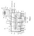
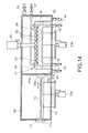
- numeral 41denotes a closed container forming a processing container composed of a lid body 41 a and a lower container 41 b
- a mounting table 42forming a mounting portion for the wafer W is provided in the lower container 41 b
- the mounting table 42is provided with, for example, three ascending and descending pins 43 raised and lowered by a raising and lowering mechanism 43 a to transfer the wafer W to the mounting table 42 , and exhaust paths 44 including valves V 1 are formed around the mounting table 42 .
- the aforesaid lid body 41 ais configured to be ascendable and descendable by means of a raising and lowering mechanism 45 via a raising and lowering shaft 45 a , and a light source unit 5 A is provided almost at the center of the lid body 41 a to face the mounting table 42 .
- the light source unit 5 Ais formed to be larger than, for example, the wafer W, and includes, for example, light sources and a reflector 51 .
- the light sourceirradiates the wafer W on the mounting table 42 with light such as an ultraviolet ray
- the reflector 51is formed of a material, for example, an aluminum evaporation film or the like, which reflects the light irradiated from the light source.
- the reflector 51is formed with almost semi-sphere shaped recessed portions 52 over its entire face, and, for example, excimer UV lamps 53 forming the aforesaid light sources are provided in the recessed portions 52 , thereby constituting the light source unit 5 A.
- the shape of the recessed portion 52is made so that the light from the UV lamp 53 is reflected on an inner face of the recessed portion 52 to reach the wafer W on the mounting table 42 , whereby the wafer W on the mounting table 42 is irradiated with the direct light from the UV lamp 53 and the light reflected on the reflector 51 .
- the light irradiated from the light sourcehere refers to light with a short wavelength and high energy, for example, light with a wavelength ranging from 150 nm to 365 nm.
- a low-pressure mercury lamp, a noble gas short arc lamp, a microwave excitation Hg—Cd lamp, or the like, in addition to the excimer UV lamp,can be used as the light source.
- an inert gassuch as helium gas, argon gas, or the like, in addition to nitrogen gas, can be used as a gas which does not absorb light.
- the lid body 41 ais formed with four gas supply paths 46 forming a hydrophobic processing gas supply portion at a plurality of positions, for example, outside a region where the reflector 51 is formed, for example, positions created by equally dividing the periphery thereof into four, the gas supply path 46 composed of a flexible pipe and is connected to a not shown gas supply source through a gas supply pipe 47 provided with a valve V 2 .
- the gas supply paths 46are formed to incline inward toward the lower side inside the lid body 41 a , whereby the gas from the gas supply paths 46 reach the entire front face of the wafer W.
- the aforesaid closed container 41is covered with a cover body 54 forming a processing chamber, and the cover body 54 is formed with a wafer transport opening 55 which is opened and closed by a shutter 55 a , and is connected to a gas supply pipe 78 forming a gas supply portion provided with a valve V 3 for supplying into the cover body 54 the aforesaid gas, for example, nitrogen gas, which does not absorb the aforesaid light (ultraviolet ray), and exhaust pipes 56 provided with valves V 4 .
- a gas supply pipe 78forming a gas supply portion provided with a valve V 3 for supplying into the cover body 54 the aforesaid gas, for example, nitrogen gas, which does not absorb the aforesaid light (ultraviolet ray), and exhaust pipes 56 provided with valves V 4 .
- a not shown controllerperforms the opening and closing operation of the shutter 55 a , the raising and lowering operations of the raising and lowering mechanisms 43 a and 45 , the ON/OFF operation of a power source 43 b of the UV lamps 53 , and the opening and closing operations of the valves V 1 to V 4 .
- numeral 24denotes a cup, in which a rotatable spin chuck 25 having a vacuum suction function is provided.
- the spin chuck 25is configured to be ascendable and descendable by means of a raising and lowering mechanism 26 , and while it stays above the cup 24 , the wafer W is transferred between the spin chuck 25 and an arm 35 described later of the aforesaid substrate transporter MA.
- Numeral 27denotes a discharge nozzle of a resist solution, numeral 28 a resist solution supply pipe, and numeral 29 a support arm for horizontally moving the nozzle.
- the discharge nozzle 27is configured to supply the resist solution, for example, near the center the wafer W, so that the resist solution is dripped from the discharge nozzle 27 to the front face of the wafer W on the spin chuck 25 and the spin chuck 25 is rotated to thereby extend the resist solution over the wafer W for coating.
- the developing unit Dhaving almost the same configuration as that of the coating unit C, in which a discharge nozzle 27 is configured to include many supply ports arranged in a direction of a diameter of the wafer W, and a developing solution is discharged from the discharge nozzle 27 to the front face of the wafer W on a spin chuck 25 and the spin chuck 25 is rotated a half turn, thereby applying the developing solution onto the wafer W, resulting in formation of a solution film of the developing solution.
- the aforesaid substrate transporter MAincluding, for example, three arms 35 for holding the wafer W, a base 36 for supporting the arms 35 and allowing them to be movable back and forth, and a pair of guide rails 37 and 38 for supporting the base 36 and for allowing them to be ascendable and descendable, is configured to be movable back and forth, to be ascendable and descendable, to be rotatable around the vertical axis by rotating the guide rails 37 and 38 by means of a rotation driver 39 .
- the interface station S 3is connected next to the processing station S 2 , and the aligner S 4 forming an aligner portion for exposing the wafer W formed with a resist film to light is connected to the interface station S 3 on the back side of the interface station S 3 .
- the interface station S 3includes the transport arm A for transferring the wafer W between the aforesaid shelf unit R 2 in the processing station S 2 and the aligner S 4 so as to transfer the wafer W between the processing station S 2 and the aligner S 4 .
- the cassette 22 housing, for example, 25 wafers Wis first carried into the cassette stage 21 by an automatic transport robot (or an operator), and the wafer W is taken out of the cassette 22 by the transfer arm 23 to be mounted on the transfer unit 33 of the shelf unit R 1 in the processing station S 2 .
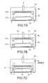
- the wafer Wis transported by the substrate transporter MA to the cleaning and hydrophobing unit U of the shelf unit R, where cleaning processing and hydrophobic processing for the front face of the wafer W are successively performed in this order.
- the valves V 3 and V 4are opened first to introduce nitrogen gas from the gas supply pipe 78 into the cover body 54 with an atmosphere in the cover body 54 being exhausted via the exhaust pipes 56 .
- the shutter 55 a of the cover body 54is opened, and the lid body 41 a of the closed container is raised, and then the substrate transporter MA carries in the wafer W through the wafer transport opening 55 and transfers it onto the mounting table 42 by combined operations thereof with the ascending and descending pins 43 .
- the shutter 55 ais closed to exchange the atmosphere inside the cover body 54 for nitrogen gas.
- the lid body 41 a of the closed containeris raised to adjust a distance L between the front face of the wafer W on the mounting table 42 and the lower end of the UV lamp 53 to a predetermined value.
- the UV lamps 53are turned on to irradiate the wafer W with ultraviolet rays with a wavelength of 172 nm for a predetermined period of time at a predetermined amount of irradiation electric power, thereby cleaning the wafer W.
- the strength of the UV lamp 53is 100 mW/cm2, the distance L between the UV lamp 53 and the wafer W is 2 mm, and the period of irradiation is 10 seconds, and, from an experimental example described later, it is preferable that the strength of the UV lamp 53 is 5 mW/cm2 to 120 mW/cm2, in this case the distance L between the UV lamp 53 and the wafer W being preferably 2 mm to 5 mm and the period of irradiation preferably 10 seconds to 30 seconds.
- the nitrogen gas atmosphererefers to an atmosphere having a nitrogen concentration higher than that of natural air, and the nitrogen concentration is preferably 90% or higher. Under the above-described conditions, the wafer W is irradiated with ultraviolet rays, whereby deposits such as organic substances on the front face of the wafer W are removed as described later.
- the lid body 41 ais lowered to close the closed container 41 , and then the valves V 1 and V 2 are opened to supply a hydrophobic processing gas, for example, HMDS (hexamethyldisilazane) gas from the gas supply pipe 47 through the gas supply paths 46 into the closed container 41 with the atmosphere inside the closed container 41 being exhausted through the exhaust paths 44 .
- HMDShexamethyldisilazane
- the above-described contact between the front face of the wafer W and the HMDS gasenhances hydrophobic properties of the substrate.
- the enhancement of the hydrophobic propertiesis enhancement an interfacial angle of contact with water, thereby enhancing adhesion between the resist and the front face of the wafer W, and preventing the developing solution from entering a resist-wafer W interface during the development.
- the hydrophobic processingis performed prior to coating with the resist solution to enhance adhesion between the wafer W and the resist to prevent a resist mask from flaking off the wafer W during a following developing step, and an ion-implanting step and an etching step to be performed thereafter.
- valve V 2is closed to stop the introduction of the HMDS gas, and the inside of the closed container 41 is sufficiently exhausted to prevent the HMDS gas from leaking outside because the HMDS gas has an amine group.
- the lid body 41 ais raised to open the closed container 41 and the shutter 55 a , and the wafer W is carried out through the wafer transport opening 55 by the substrate transporter MA.
- the exhaustion and the introduction of nitrogen gasare being performed inside the cover body 54 .
- the wafer Wis subsequently transported via the cooling unit 32 of the shelf unit R, the substrate transporter MA to the coating unit C, whereby the wafer W which has been subjected to temperature adjustment is coated with the resist solution at a predetermined temperature, for example, 23° C. Thereafter, the wafer W is transported via the substrate transporter MA, the heating unit 31 of the shelf unit R, the substrate transporter MA to the cooling unit 32 of the shelf unit R to thereby subjected to temperature adjustment, and subsequently, the wafer W is transported via the substrate transporter MA, the transfer unit 34 of the shelf unit R 2 , the transport arm A of the interface station S 3 to the aligner S 4 to be subjected to exposure.
- a predetermined temperaturefor example, 23° C.
- the wafer W after the exposureis transported via the aligner S 4 , the transport arm A of the interface station S 3 , the transfer unit 33 of the shelf unit R 2 , the substrate transporter MA, the heating unit 31 of the shelf unit R, the cooling unit 32 to the developing unit D, whereby the wafer W is subjected to temperature adjustment by being first heated to a predetermined temperature and then cooled to a predetermined temperature, and is subjected to developing processing at a predetermined temperature, for example, 23° C. which is a coating temperature of the developing solution in the developing unit D.
- the wafer Wis thereafter transported via the substrate transporter MA, the heating unit 32 of the shelf unit R, the substrate transporter MA, the cooling unit 32 of the shelf unit R, the substrate transporter MA, the transfer unit 34 of the shelf unit R 1 to the transfer arm 23 , whereby the wafer W, which has been once heated to a predetermined temperature and then cooled to a predetermined temperature, is returned into, for example, the original cassette 22 through the transfer unit 33 .
- the wafer Wis cleaned by being irradiated with ultraviolet rays prior to the coating with the resist solution, so that organic substances adhering to the wafer W, for example, in the clean room atmosphere can be removed.
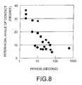
- FIG. 8is a characteristic chart showing effects of organic substance removal by ultraviolet-ray irradiation to a thermal oxide film wafer contaminated by organic substances, and a horizontal axis and a vertical axis in the chart indicate the period of irradiation with ultraviolet rays and the interfacial angle of contact respectively.
- the interfacial angle of contactrefers to an angle obtained by doubling the angle formed by a line which connects the crest of a waterdrop dripped on the front face of the substrate and the outer edge on the front face of the substrate with the front face of the substrate, and it is shown that the greater the interfacial angle of contact is, the greater is the amount of organic substances adhering to the substrate.
- the strength of the ultraviolet rayswas about 100 mW/cm2, and the experiment was carried out changing the distance L between the substrate and the UV lamp 53 to 2 mm, 5 mm, and 10 mm.
- nitrogen gas which does not absorb the ultraviolet raysis introduced into an irradiation region between the wafer W and the UV lamps during the irradiation with the ultraviolet rays to bring the region to a nitrogen gas atmosphere, so that the concentration of gas, for example, water vapor or oxygen, which absorbs the ultraviolet rays within the region, decreases, resulting in enhanced irradiation efficiency of the ultraviolet rays.
- Thiscan shorten the period of time required for the cleaning processing, thereby suppressing deterioration of throughput in the above-described coating and developing apparatus.
- the nitrogen gasis introduced here to prevent light with a wavelength 200 nm or shorter from being absorbed by oxygen or water so as to enhance the irradiation efficiency, and further an effect of inhibiting oxidation of the wafer W can also be obtained.
- FIGS. 10A, 10 B, and 10 Care mass analysis spectra obtained by a gas chromatograph/mass spectrograph to check the effect of organic substance removal by the ultraviolet ray irradiation in the nitrogen atmosphere.
- FIG. 10Ashows a spectrum of the wafer W left standing in a clean room
- FIG. 10Ba spectrum when the wafer W is laid in an oxygen atmosphere (oxygen concentration of 95% or higher) and irradiated with ultraviolet rays
- FIG. 10Ca spectrum when the wafer W is laid in a nitrogen atmosphere (nitrogen concentration of 99% or higher) and irradiated with ultraviolet rays, respectively.
- the strength of the ultraviolet rayswas 100 mW/cm2
- the period of irradiationwas 10 seconds
- the distance L between the substrate and the UV lamp 53was 2 mm.
- the position and the magnitude of a peakshow the kind of organic substance and the amount of adherence of the organic substances respectively, and it is shown that the larger the number of peaks is and the greater the magnitude of the peak is, the greater is the amount of adherence of the organic substances.
- the number of peaksis smallest and the magnitude of the peak is smallest in the case of irradiation with the ultraviolet rays in the nitrogen atmosphere. This provides an understanding of the fact that the irradiation efficiency of the ultraviolet ray is high in the nitrogen atmosphere, and thus the efficiency of cleaning of the organic substances is high.
- the cleaning unit and the hydrophobing unitcan be united in the same unit as in the above-described embodiment, thereby downsizing the apparatus in this case compared with the case in which the cleaning unit and the hydrophobing unit are separately provided. Further, the transport of the wafer W between the cleaning unit and the hydrophobing unit becomes unnecessary, thereby omitting the transporting step to improve the throughput further, and, more than that, preventing occurrence of re-adherence of the organic substances during the transport of the wafer W from the cleaning unit to the hydrophobing unit, so that the hydrophobic processing can be performed with the cleanliness of the wafer W being maintained.
- the reflector 51is provided on the opposite side to the side facing the wafer W of the UV lamps 53 , the light scattering from the UV lamps 53 is reflected by the reflector 51 to reach the wafer W, thereby further improving the irradiation efficiency of the ultraviolet rays, resulting in a shorter period of cleaning time.
- the cleaning and hydrophobing unit Umay be configured as that, for example, shown in FIG. 11 or in FIG. 12 .
- An example shown in FIG. 11is the one in which a gas supply chamber 61 forming the hydrophobic processing gas supply potion and a light source unit 5 B are provided in combination with the lid body 41 a .
- the gas supply chamber 61is provided almost at the center of the lid body 41 a
- the light source unit 5 Bis provided, for example, annularly outside the gas supply chamber 61 .
- the light source unit 5 Bis configured the same as for the light source unit 5 A in the aforesaid embodiment, in which the gas supply chamber 61 includes many gas supply ports 62 at the lower face and is connected to a not shown gas supply source through a gas supply pipe 47 constituted of a flexible pipe.
- the UV lamps 53 of the light source unit 5 Bare turned ON first to perform cleaning processing for the wafer W, and thereafter HMDS gas is supplied to the wafer W through the gas supply chamber 61 to perform hydrophobic processing.
- the HMDS gasis supplied to the wafer W from the gas supply chamber 61 provided almost at the center of the lid body 41 a , so that the HMDS gas evenly contacts the front face of the wafer W to enhance the uniformity in the hydrophobic processing.
- a condensing member(not shown), for example, a lens or the like may be provided to irradiate the center of the wafer W with the ultraviolet rays in this embodiment, in which the uniformity in the cleaning processing also improves.
- FIGS. 12A and 12BAn embodiment shown in FIGS. 12A and 12B is an example, in which a gas supply unit 6 forming the hydrophobic processing gas supply portion and a light source unit 5 C are detachably provided at the lid body 41 a to be movable between a position where these units are attached to the lid body 41 a and a position where they wait after being detached from the lid body 41 a by means of a not shown moving mechanism.
- the gas supply unit 6is configured the same as for the aforesaid gas supply chamber 61 shown in FIG. 11, and the light source unit 5 C is configured the same as for the light source unit 5 A shown in FIG. 4, and they are formed in a size attachable to an attachment opening 63 formed in the lid body 41 a.
- the light source unit 5 Cis first attached to the lid body 41 a to perform predetermined processing, and then the light source unit 5 C is detached and the gas supply unit 6 is attached to perform predetermined hydrophobic processing.
- the ultraviolet rays and the HMDS gasare supplied to the wafer W respectively from the light source unit 5 C and the gas supply unit 6 which are provided almost at the center of the lid body 41 a , thereby enhancing the uniformity in the cleaning processing and the hydrophobic processing.
- a cleaning unit 7 B for performing cleaning processing and a hydrophobing unit 7 C for performing hydrophobic processingare separately provided in a cover body 7 A, and an exclusive transport arm A 1 transfers the wafer W between the above units.
- the cover body 7 Ais provided with a load lock chamber 7 D on the side facing a substrate transporter MA, and the cleaning unit 7 B and the hydrophobing unit 7 C are provided on the front side and on the back side respectively, as seen from the load lock chamber 7 D side, and the transport arm A 1 is provided between them in the cover body 7 A.
- numeral 70denotes a wafer transport opening of the cover body 7 A
- numeral 71a wafer transport opening of the load lock chamber 7 D
- numerals 70 a and 71 aare respective shutters.
- a transport plate 72which is configured to be movable back and forth for transferring the wafer W between the substrate transporter MA and the cleaning unit 7 B.
- the transport plate 72is formed like a comb having, for example, three teeth, so that, for example, three ascending and descending pins 73 , which are raised and lowered by a raising and lowering mechanism 73 a composed of, for example, a cylinder, protrude between the teeth in such a manner not to interfere the teeth to transfer the wafer W to the plate 72 by combined operations with the substrate transporter MA.
- the aforesaid cleaning unit 7 Bincludes a mounting table 74 forming a mounting portion for the wafer W and a light source unit 75 provided to face the mounting table 74 .
- the mounting table 74includes, for example, three ascending and descending pins 76 which are raised and lowered by a raising and lowering mechanism 76 a , for transferring the wafer W to/from the mounting table 74 , and the ascending and descending pins 76 are provided at positions where they do not interfere the teeth of the transport plate 72 when the transport plate 72 enters the cleaning unit 7 B to transfer the wafer W thereto.
- the light source unit 75is configured, for example, the same as in the aforesaid embodiment (the same numerals and symbols are given to the same members).
- the distance L between the light source 75 and the wafer W on the mounting table 74is previously set to a predetermined value, but the light source unit 75 may be provided to ascend and descend freely by means of a not shown raising and lowering mechanism to change the distance L.
- the hydrophobing unit 7 Chas the same configuration as that of the cleaning and hydrophobing unit U shown in FIG. 4 other than that a gas supply unit 40 forming a hydrophobic processing gas supply portion connected to a not shown gas supply source through a gas supply pipe 47 composed of a flexible pipe is provided almost at the center of a lid body 41 a , and thus the same numerals and symbols are given to the same members.
- the gas supply unit 40is configured in the same manner as the aforesaid gas supply chamber 61 in FIG. 11 .
- the transport arm A 1includes one arm 77 for holding the wafer W and is configured to be movable back and forth, ascendable and descendable, and rotatable around the vertical axis to transfer the wafer W between the cleaning unit 7 B and the hydrophobing unit 7 C.
- the ascending and descending pins 73first wait for the wafer W to be carried into the load lock chamber 7 D with protruding from the transport plate 72 , and then the shutter 71 a is opened for the wafer W to be transferred onto the ascending and descending pins 73 , and thereafter the shutter 71 a is closed and the ascending and descending pins 73 are lowered to thereby mount the wafer W on the transport plate 72 . Then, the shutter 70 a is opened to allow the transport plate 72 to enter the cover body 7 A side, and, after the completion of movement of the plate 72 , the ascending and descending pins 76 of the cleaning unit 7 B are protruded and the wafer W is transferred thereto.
- the transport plate 72is retracted to the load lock chamber 7 D side, and then the shutter 70 a is closed.
- the valves V 5 and V 6are opened in the cover body 7 A to exchange the inside the cover body 7 A for a nitrogen atmosphere.
- the UV lamps 53are turned on to perform predetermined cleaning processing
- the lid body 41 a of the hydrophobing unit 7 Cis then opened for the transport arm A 1 to transfer the wafer W onto the mounting table 42 of the hydrophobing unit 7 C, and then the lid body 41 a is closed.
- the valves V 1 and V 2are opened to supply the HMDS gas to perform predetermined hydrophobic processing.
- HMDS gasis stopped and the inside of a closed container 41 is sufficiently exhausted, and then the lid body 41 a is opened to carry out the wafer W from the wafer transport opening 71 through the transport arm A 1 , the mounting table 74 of the cleaning unit 7 B, the transport plate 72 of the load lock chamber 7 D.
- a wafer transport opening not shownmay be provided to transfer the wafer W, for which the hydrophobic processing has been completed, from the hydrophobing unit 7 C directly to the substrate transporter MA, and in this case a second load lock chamber may be provided on the transport opening side.
- a load lock chambermay be provided for each cover body, for example, as shown in FIG. 14 .
- the example shown in FIG. 14is an example made by combination of the cover body 54 of the unit in FIG. 4 and the load lock chamber 50 of the unit in FIG. 13, and thus the same numerals and symbols are given to the same members.
- a hydrophobing unit 8 A and a cleaning unit 8 Bare multi-tiered in shelves, and an exclusive transport arm A 2 transfers the wafer W between these units through an exclusive transport path E.
- two hydrophobing units 8 A and one cleaning unit 8 Bare multi-tiered with the hydrophobing units 8 A at the upper tiers, and the transport path E exclusive for the transport arm A 2 is formed on the different side from the side facing the substrate transporter MA of the hydrophobing units 8 A and the cleaning unit 8 B.
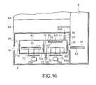
- the cleaning unit 8 Bas shown in FIG. 16, includes a load lock chamber 8 C at a position corresponding to the substrate transporter MA, and includes a cleaning chamber 8 D on the back side of the load lock chamber 8 C, as seen from the substrate transporter MA, and further the transport path E for the transport arm A 2 is formed on the back side of the cleaning chamber 8 D.
- the load lock chamber 8 C and the cleaning chamber 8 Dare provided in a shelf 8 formed with wafer transport openings 81 and 82 at positions corresponding to the substrate transporter MA and to the transport arm A 2 respectively, and a wafer transport opening 83 including a shutter 83 a is formed on the side facing the transport path E for the transport arm A 2 of the cleaning chamber 8 D.
- the rest of the configurationis the same as that of the aforesaid embodiment shown in FIG. 13 other than for the absence of, for example, the hydrophobing unit, and thus the same numerals and symbols are given to the same members.
- Each of the two hydrophobing units 8 Ais also provided in a shelf 8 formed with wafer transport openings (not shown) at positions corresponding to a position facing the substrate transporter MA and to a position corresponding to the transport arm A 2 respectively, and the rest of the configuration is the same as that of the aforesaid embodiment shown in FIG, 13 other than for the absence of, for example, the cleaning unit.
- the transport arm A 2includes one arm 84 for holding the wafer W which is configured to be movable back and forth and to be ascendable and descendable to transfer the wafer W between the cleaning unit 8 B and the hydrophobing units 8 A.
- the wafer Wis transported to the cleaning chamber 8 D through the load lock chamber 8 C to perform predetermined cleaning processing under a predetermined nitrogen atmosphere. Thereafter, the wafer W is transferred to the transport arm A 2 through the wafer transport opening 83 , and after the shutter 83 a is closed, the transport arm A 2 transports the wafer W to the hydrophobing unit 8 A through the exclusive transport path E. After the predetermined processing is completed in the hydrophobing unit 8 A, the wafer W is transferred to the substrate transporter MA through the wafer transport opening of the shelf 8 to be transported to the next step.
- the hydrophobing units 8 A and the cleaning unit 8 Bmay be provided at any of the shelf units R 1 to R 3 , or a shelf unit R including the hydrophobing units A and the cleaning unit 8 B may be separately provided. Further, the numbers of the hydrophobing units 8 A and the cleaning units 8 B are not limited to that of the above-described example, and further nitrogen gas may be supplied to the exclusive transport path E to bring its transport space to a nitrogen atmosphere.
- the effects of organic substance removal by irradiation with the ultraviolet rays and improvement in the cleaning efficiency by virtue of the introduction of the nitrogen gascan be obtained as in the aforesaid embodiments, and the plurality of hydrophobing units 8 A and the cleaning unit 8 B are multi-tiered and the common transport arm A 2 transports the wafer W between them, thereby downsizing the apparatus. Further, the wafer is less susceptible to re-contamination during the transport because of existence of the exclusive transport path E. Furthermore, the wafer transport opening corresponding to the substrate transporter MA and the wafer transport opening corresponding to the transport arm A 2 are separately provided in the shelf 8 in this embodiment, and thus the transport between them can be smoothly performed, resulting in improved throughput.
- the cleaning and hydrophobing unit Umay be equipped with a vacuum pump 91 for reducing a pressure in the unit.
- the vacuum pump 91preferably reduces the pressure in the unit to about 10 ⁇ 4 torr to perform the hydrophobic processing.
- the hydrophobing processingis performed under a reduced pressure, whereby a partial pressure of the hydrophobic processing gas rises, facilitating attachment of the gas to the wafer W, resulting in enhanced interfacial angle of contact.
- it is more preferable that the pressure inside the unitis first reduced and then the hydrophobic processing gas is introduced into the unit in the above-described processing. This can eliminate waste of the hydrophobic processing gas.
- an anti-reflection coatingmay be formed, in place of the hydrophobic processing, on the front face of the wafer W prior to the coating with the resist.
- the anti-reflection coatingis formed to prevent reflection from occurring on the lower side of a resist during the exposure when a chemically amplified resist is used.
- the substrateis not limited to the wafer but it may be a glass substrate for a liquid crystal display.
- the front face of the substrateis irradiated with light, thereby removing deposits such as organic substances adhering to the substrate to thereby improve the quality of the substrate and perform the cleaning of the substrate uniformly, resulting in enhanced coating properties of the resist solution.
- the gas which does not absorb lightis introduced into a light irradiation space between the light source and the substrate, thereby improving irradiation efficiency of the light, shortening the period of cleaning time, and further preventing oxidation of the substrate.
Landscapes
- Engineering & Computer Science (AREA)
- Physics & Mathematics (AREA)
- General Physics & Mathematics (AREA)
- Computer Hardware Design (AREA)
- Condensed Matter Physics & Semiconductors (AREA)
- Manufacturing & Machinery (AREA)
- Microelectronics & Electronic Packaging (AREA)
- Power Engineering (AREA)
- Optics & Photonics (AREA)
- Exposure Of Semiconductors, Excluding Electron Or Ion Beam Exposure (AREA)
- Cleaning Or Drying Semiconductors (AREA)
- Photosensitive Polymer And Photoresist Processing (AREA)
- Drying Of Semiconductors (AREA)
- Application Of Or Painting With Fluid Materials (AREA)
- Coating Apparatus (AREA)
Abstract
Description
1. Field of the Invention
The present invention relates to a substrate processing method and a substrate processing apparatus each for performing coating processing of, for example, a resist solution, developing processing, and the like for a substrate such as a semiconductor wafer, a glass substrate for a liquid crystal display, or the like.
2. Description of the Related Art
In the photolithography technology in processes of semiconductor device fabrication, a resist is applied to the front face of a semiconductor wafer (hereinafter, referred to as a “wafer”), the applied resist is subjected to exposure processing into a predetermined pattern and further to developing processing, thereby forming a resist film in the predetermined pattern. Such a series of processing is performed by a system in which an aligner is connected to a coating/developing apparatus.
FIG. 17 is a plan view showing an example of the above-described system, in which a cassette C housing therein substrates, for example, 25 wafers W is carried into acassette stage 1 in a cassette station A1. A processing station A2 is connected to the cassette station A1, and further an aligner not shown is connected to the processing station A2 through an interface station A3.
A wafer W in the cassette station C on thecassette stage 1 is taken out by atransfer arm 11 and sent via a transfer unit of ashelf unit 12 to acoating unit 13, where a resist is applied thereto. Thereafter, the wafer W is transported via a wafer transporter MA, a transfer unit of ashelf unit 14, the interface station A3, to the aligner to be exposed to light. The wafer W after the exposure is transported via a reverse route to the processing station A2, and developed in a developing unit not shown provided at the tier under thecoating unit 13, and thereafter the wafer W is transported via the wafer transporter MA, the transfer unit of theshelf unit 12 to the cassette C.
It should be noted that shelves of theshelf units shelf units numeral 15 denotes a transfer arm for transferring the wafer W between the processing station A2 and the aligner.
It is well known that organic substances adhere to the wafer W in a clean room atmosphere, the organic substances causing occurrence of flaking-off of the resist and coating particles, and thus there has been a great demand for removal of such organic substances. For the demand, it is more typical to clean the wafer W to thereby remove the organic substances, but the cleaning by a solution is often improper depending on the kind of films. Thus, the present inventor has developed a technique of removing the organic substances by irradiating the wafer W with an ultraviolet ray.
What is well known as the above-described UV cleaning apparatus is, for example, the configuration in which the wafer W on the mounting table is irradiated with the ultraviolet ray by a UV lamp for a predetermined period of time in a processing chamber of an atmosphere of natural air or an oxygen-rich atmosphere in a processing chamber. When this cleaning apparatus is installed into the aforesaid system, it is conceivable to dispose the apparatus, for example, in theshelf unit cassette stage 1, the transfer unit of theshelf unit 12, the cleaning apparatus, the hydrophobing unit, to the coating unit.
The cleaning apparatus, however, has a poor cleaning efficiency because of existence of gasses such as water vapor and oxygen which absorb the ultraviolet rays in the processing chamber, and thus it requires a period of cleaning, for example, 60 seconds to remove, to a predetermined amount or less, the organic substances adhering to the wafer W. Thus, the installation of the apparatus into the aforesaid coating and developing apparatus increases a period of time of the wafer W waiting for transport in the other units, whereby throughput is susceptible to deterioration. It is conceivable to increase the irradiation energy of the UV lamp in this event, but the power consumption also increases, presenting a problem in cost.
An object of the present invention is to provide a substrate processing method for removing deposits on a substrate in a short period of cleaning to improve coating properties of a resist solution and an apparatus therefor.
Thus, a substrate processing method of the present invention is characterized by comprising the steps of:
irradiating a front face of a substrate with a light from a light source to thereby remove a deposit on the front face of the substrate; subsequently, coating the front face of the substrate with a resist solution;
performing exposure processing for the substrate which has been coated with the resist solution; and
performing developing processing for the substrate after the exposure to obtain a resist pattern, wherein the step of removing the deposit on the front face of the substrate is performed while a gas absorbing no light is being introduced into a light irradiation space between the light source and the substrate. In this event, the light irradiated onto the front face of the substrate comprises an ultraviolet ray, and the gas absorbing no light comprises an inert gas.
In the above-described method, the front face of the substrate is irradiated with light, so that the deposits such as organic substances adhering to the substrate, for example, in a clean room atmosphere can be removed, resulting in improved coating properties of the resist solution. In this event, the gas absorbing no light is introduced into the light irradiation space between the light source and the substrate, thereby improving irradiation efficiency of the light, shortening the period of cleaning, and preventing oxidation of the substrate.
It is suitable to perform the step of supplying a hydrophobic processing gas to the front face of the substrate to perform hydrophobic processing for the front face between the step of removing the deposit on the front face of the substrate and the step of coating the front face of the substrate with the resist solution, and in this case the quality of the front face of the substrate is improved by the irradiation with light, resulting in improved coating properties of the hydrophobic processing gas in the hydrophobic processing.
The above-described substrate processing method is carried out in a substrate processing apparatus comprising: a cleaning and hydrophobing unit including a cleaning unit, having a light source for irradiating a substrate with a light and a gas supplier for introducing gas absorbing no light into a light irradiation space between the light source and the substrate, for irradiating the front face of the substrate with the light from the light source to thereby remove a deposit on the front face of the substrate, and a hydrophobing unit for supplying a hydrophobic processing gas to the front face of the substrate to perform hydrophobic processing for the front face; a coater for coating the front face of the substrate with a resist solution; and a developer for performing developing processing for the substrate which has been coated with the resist solution and subjected to exposure processing to obtain a resist pattern.
For example, the unit including the cleaning unit and the hydrophobing unit here comprises: a processing container including a mounting table for holding the substrate; a light source for irradiating the substrate held on the mounting table with the light; a hydrophobic processing gas supplier for supplying the hydrophobic processing gas to the substrate held on the mounting table; and the gas supplier for introducing the gas absorbing no light into the light irradiation space between the light source and the substrate, wherein the front face of the substrate is irradiated with the light from the light source while the gas absorbing no light is being introduced into the irradiation space, and subsequently the hydrophobic processing gas is supplied to the front face of the substrate.
Further, a substrate transporter for transporting the substrate between the cleaning unit and the hydrophobing unit may be provided, and in the case where the cleaning unit and the hydrophobing unit are provided in the same processing chamber, the apparatus can be downsized.
Further the cleaning unit and the hydrophobing unit may be provided in different processing chambers, and a transporter may transport the substrate between the cleaning unit and the hydrophobing unit through an exclusive transport path.
These objects and still other objects and advantages of the present invention will become apparent upon reading the following specification when taken in conjunction with the accompanying drawings.
FIG. 1 is a schematic plan view showing a coating and developing apparatus according to an embodiment of the present invention;
FIG. 2 is a schematic perspective view showing the coating and developing apparatus;
FIG. 3 is a side view showing an example of a shelf unit of the coating and developing apparatus;
FIG. 4 is a sectional view showing an example of a cleaning and hydrophobing unit;
FIG. 5 is a sectional view showing an example of a coating unit;
FIG. 6 is a sectional view showing a substrate transporter;
FIGS. 7A to7C are sectional views for explaining operations of the cleaning and hydrophobing unit;
FIG. 8 is a characteristic chart showing effects of organic substance removal by ultraviolet ray irradiation;
FIG. 9 is a characteristic chart showing a relation between a distance L between a wafer and a light source unit and performance of organic substances removal;
FIGS. 10A to10C are characteristic charts of effects of organic substance removal by ultraviolet ray irradiation under a nitrogen atmosphere;
FIG. 11 is a sectional view showing another embodiment of the cleaning and hydrophobing unit;
FIGS. 12A and 12B are sectional views showing still another embodiment of the cleaning and hydrophobing unit;
FIG. 13 is a sectional view showing still another embodiment of the cleaning and hydrophobing unit;
FIG. 14 is a sectional view showing still another embodiment of the cleaning and hydrophobing unit;
FIG. 15 is a side view showing still another embodiment of the cleaning and hydrophobing unit;
FIG. 16 is a sectional view of the cleaning and hydrophobing unit;
FIG. 17 is a schematic plan view showing a conventional coating and developing apparatus; and
FIG. 18 is a sectional view showing still another embodiment of the cleaning and hydrophobing unit.
Hereinafter, embodiments applied to a coating and developing apparatus for a substrate will be explained.
FIG. 1 is a schematic plan view of this embodiment, and FIG. 2 is a schematic perspective view revealing the inside thereof, in each of which S1 denotes a cassette station, S2 a processing station for performing coating processing of a resist and developing processing for a wafer W, S3 an interface station, and S4 an aligner.
The cassette station S1 comprises acassette stage 21 for mounting thereon, for example, four wafer cassettes (hereinafter, referred to as “cassettes”)22, each housing a plurality of substrates, for example, 25 wafers W, and atransfer arm 23 for transferring the wafer W between thecassette 22 on thecassette stage 21 and the processing station S2. Thetransfer arm 23 is configured to be ascendable and descendable, movable in X- and Y-directions, and rotatable around the vertical axis.
The processing station S2, including, for example, two coating units C (C1 and C2) forming coating processing portions, two developing units D (D1 and D2) forming developing processing portions, for example, three shelf units R (R1, R2, and R3), and, for example, one substrate transporter MA, is configured to transfer the wafer W between the cassette station S1 and the interface station S3 and perform processing of cleaning the wafer W, processing of hydrophobing the front face of the wafer W, processing of coating the wafer W with a resist solution, developing processing of the wafer W, processing of heating the wafer W to a predetermined temperature before and after the above processings and cooling it in the station S2.
Explaining an example of the layout of the above-described processing station S2, on the back side of theaforesaid transfer arm 23, for example, processing units, including the coating units C and the developing units D and the like, are provided in two tiers, for example, on the right side as seen from, for example, the cassette station S1 toward the back. In other words, the two coating units C1 and C2 are disposed side by side in a direction almost orthogonal to the direction of arrangement of the cassettes on thecassette stage 21 with the coating unit C1 on the front side. At the tiers under the coating units C1 and C2, the two developing units D1 and D2 are disposed side by side with the developing unit D1 on the front side. Incidentally, the explanation hereafter will be given assuming that the cassette station S1 side is designated the front side and the aligner S4 side the back side.
On the left side of the processing units as seen from the cassette station S1, provided is the substrate transporter MA, which is, for example, ascendable and descendable, movable laterally and longitudinally, and rotatable around the vertical axis, for transferring the wafer W between the coating units C, the developing units D, and the shelf units R. The shelf unit R1, the shelf unit R2, and the shelf unit R3 are disposed on the front side, on the back side, on the left side of the substrate transporter MA respectively as seen from the cassette station S1 side. The shelf unit R3 and the substrate transporter MA, however, are omitted in FIG. 2 for convenience.
In the aforesaid shelf units R (R1, R2, and R3), as in the shelf unit R1 shown in FIG. 3,heating units 31 for heating the wafer W, coolingunits 32 for cooling the wafer W, cleaning and hydrophobing units U for cleaning and hydrophobing the front face of the wafer, transferringunits 33 including transfer tables for transferring the wafer W between thetransfer arm 23 of the cassette station S1 and the substrate transporter MA in the shelf unit R1, and for transferring the wafer W between a transfer arm A of the interface station S3 described later and the substrate transporter MA in the shelf unit R2, and analignment unit 34 for aligning the wafer W in the shelf unit R1 are vertically arranged.
Explaining the aforesaid cleaning and hydrophobing unit U with reference to FIG. 4, numeral41 denotes a closed container forming a processing container composed of alid body 41aand alower container 41b, and a mounting table42 forming a mounting portion for the wafer W is provided in thelower container 41b. The mounting table42 is provided with, for example, three ascending and descendingpins 43 raised and lowered by a raising and loweringmechanism 43ato transfer the wafer W to the mounting table42, andexhaust paths 44 including valves V1 are formed around the mounting table42.
Theaforesaid lid body 41ais configured to be ascendable and descendable by means of a raising and loweringmechanism 45 via a raising and loweringshaft 45a, and alight source unit 5A is provided almost at the center of thelid body 41ato face the mounting table42. Thelight source unit 5A is formed to be larger than, for example, the wafer W, and includes, for example, light sources and areflector 51. The light source irradiates the wafer W on the mounting table42 with light such as an ultraviolet ray, and thereflector 51 is formed of a material, for example, an aluminum evaporation film or the like, which reflects the light irradiated from the light source. Thereflector 51 is formed with almost semi-sphere shaped recessedportions 52 over its entire face, and, for example,excimer UV lamps 53 forming the aforesaid light sources are provided in the recessedportions 52, thereby constituting thelight source unit 5A. The shape of the recessedportion 52 is made so that the light from theUV lamp 53 is reflected on an inner face of the recessedportion 52 to reach the wafer W on the mounting table42, whereby the wafer W on the mounting table42 is irradiated with the direct light from theUV lamp 53 and the light reflected on thereflector 51.
The light irradiated from the light source here refers to light with a short wavelength and high energy, for example, light with a wavelength ranging from 150 nm to 365 nm. A low-pressure mercury lamp, a noble gas short arc lamp, a microwave excitation Hg—Cd lamp, or the like, in addition to the excimer UV lamp, can be used as the light source. Further, an inert gas such as helium gas, argon gas, or the like, in addition to nitrogen gas, can be used as a gas which does not absorb light.
Thelid body 41ais formed with fourgas supply paths 46 forming a hydrophobic processing gas supply portion at a plurality of positions, for example, outside a region where thereflector 51 is formed, for example, positions created by equally dividing the periphery thereof into four, thegas supply path 46 composed of a flexible pipe and is connected to a not shown gas supply source through agas supply pipe 47 provided with a valve V2. Thegas supply paths 46 are formed to incline inward toward the lower side inside thelid body 41a, whereby the gas from thegas supply paths 46 reach the entire front face of the wafer W.
The aforesaidclosed container 41 is covered with acover body 54 forming a processing chamber, and thecover body 54 is formed with awafer transport opening 55 which is opened and closed by ashutter 55a, and is connected to agas supply pipe 78 forming a gas supply portion provided with a valve V3 for supplying into thecover body 54 the aforesaid gas, for example, nitrogen gas, which does not absorb the aforesaid light (ultraviolet ray), andexhaust pipes 56 provided with valves V4.
In the cleaning and hydrophobic processing unit U, a not shown controller performs the opening and closing operation of theshutter 55a, the raising and lowering operations of the raising and loweringmechanisms power source 43bof theUV lamps 53, and the opening and closing operations of the valves V1 to V4.
Explaining the aforesaid coating unit C with reference to FIG. 5, numeral24 denotes a cup, in which arotatable spin chuck 25 having a vacuum suction function is provided. Thespin chuck 25 is configured to be ascendable and descendable by means of a raising and loweringmechanism 26, and while it stays above thecup 24, the wafer W is transferred between thespin chuck 25 and anarm 35 described later of the aforesaid substrate transporter MA.
The developing unit D, having almost the same configuration as that of the coating unit C, in which adischarge nozzle 27 is configured to include many supply ports arranged in a direction of a diameter of the wafer W, and a developing solution is discharged from thedischarge nozzle 27 to the front face of the wafer W on aspin chuck 25 and thespin chuck 25 is rotated a half turn, thereby applying the developing solution onto the wafer W, resulting in formation of a solution film of the developing solution.
The aforesaid substrate transporter MA, as shown in FIG. 6, including, for example, threearms 35 for holding the wafer W, abase 36 for supporting thearms 35 and allowing them to be movable back and forth, and a pair ofguide rails base 36 and for allowing them to be ascendable and descendable, is configured to be movable back and forth, to be ascendable and descendable, to be rotatable around the vertical axis by rotating the guide rails37 and38 by means of arotation driver 39.
The interface station S3 is connected next to the processing station S2, and the aligner S4 forming an aligner portion for exposing the wafer W formed with a resist film to light is connected to the interface station S3 on the back side of the interface station S3. The interface station S3 includes the transport arm A for transferring the wafer W between the aforesaid shelf unit R2 in the processing station S2 and the aligner S4 so as to transfer the wafer W between the processing station S2 and the aligner S4.
Operations of the above-described embodiment will be explained next. Thecassette 22 housing, for example, 25 wafers W is first carried into thecassette stage 21 by an automatic transport robot (or an operator), and the wafer W is taken out of thecassette 22 by thetransfer arm 23 to be mounted on thetransfer unit 33 of the shelf unit R1 in the processing station S2.
The wafer W is transported by the substrate transporter MA to the cleaning and hydrophobing unit U of the shelf unit R, where cleaning processing and hydrophobic processing for the front face of the wafer W are successively performed in this order. More concretely, as shown in FIG. 7A, the valves V3 and V4 are opened first to introduce nitrogen gas from thegas supply pipe 78 into thecover body 54 with an atmosphere in thecover body 54 being exhausted via theexhaust pipes 56. In this state, theshutter 55aof thecover body 54 is opened, and thelid body 41aof the closed container is raised, and then the substrate transporter MA carries in the wafer W through thewafer transport opening 55 and transfers it onto the mounting table42 by combined operations thereof with the ascending and descending pins43. After the substrate transporter MA is retracted, theshutter 55ais closed to exchange the atmosphere inside thecover body 54 for nitrogen gas.
Then, as shown in FIG. 7B, thelid body 41aof the closed container is raised to adjust a distance L between the front face of the wafer W on the mounting table42 and the lower end of theUV lamp 53 to a predetermined value. In the sate in which the inside of theclosed container 41 has been brought to a nitrogen gas atmosphere as described above, theUV lamps 53 are turned on to irradiate the wafer W with ultraviolet rays with a wavelength of 172 nm for a predetermined period of time at a predetermined amount of irradiation electric power, thereby cleaning the wafer W.
As an example of cleaning conditions, the strength of theUV lamp 53 is 100 mW/cm2, the distance L between theUV lamp 53 and the wafer W is 2 mm, and the period of irradiation is 10 seconds, and, from an experimental example described later, it is preferable that the strength of theUV lamp 53 is 5 mW/cm2 to 120 mW/cm2, in this case the distance L between theUV lamp 53 and the wafer W being preferably 2 mm to 5 mm and the period of irradiation preferably 10 seconds to 30 seconds. The nitrogen gas atmosphere refers to an atmosphere having a nitrogen concentration higher than that of natural air, and the nitrogen concentration is preferably 90% or higher. Under the above-described conditions, the wafer W is irradiated with ultraviolet rays, whereby deposits such as organic substances on the front face of the wafer W are removed as described later.
After the cleaning of the wafer W is performed as described above, as shown in FIG. 7C, thelid body 41ais lowered to close theclosed container 41, and then the valves V1 and V2 are opened to supply a hydrophobic processing gas, for example, HMDS (hexamethyldisilazane) gas from thegas supply pipe 47 through thegas supply paths 46 into theclosed container 41 with the atmosphere inside theclosed container 41 being exhausted through theexhaust paths 44. The above-described contact between the front face of the wafer W and the HMDS gas enhances hydrophobic properties of the substrate. The enhancement of the hydrophobic properties is enhancement an interfacial angle of contact with water, thereby enhancing adhesion between the resist and the front face of the wafer W, and preventing the developing solution from entering a resist-wafer W interface during the development.
The hydrophobic processing is performed prior to coating with the resist solution to enhance adhesion between the wafer W and the resist to prevent a resist mask from flaking off the wafer W during a following developing step, and an ion-implanting step and an etching step to be performed thereafter.
Subsequently, the valve V2 is closed to stop the introduction of the HMDS gas, and the inside of theclosed container 41 is sufficiently exhausted to prevent the HMDS gas from leaking outside because the HMDS gas has an amine group. Subsequently, thelid body 41ais raised to open theclosed container 41 and theshutter 55a, and the wafer W is carried out through thewafer transport opening 55 by the substrate transporter MA. During a series of processing of the cleaning and the hydrophobic processing, the exhaustion and the introduction of nitrogen gas are being performed inside thecover body 54.
The wafer W is subsequently transported via thecooling unit 32 of the shelf unit R, the substrate transporter MA to the coating unit C, whereby the wafer W which has been subjected to temperature adjustment is coated with the resist solution at a predetermined temperature, for example, 23° C. Thereafter, the wafer W is transported via the substrate transporter MA, theheating unit 31 of the shelf unit R, the substrate transporter MA to thecooling unit 32 of the shelf unit R to thereby subjected to temperature adjustment, and subsequently, the wafer W is transported via the substrate transporter MA, thetransfer unit 34 of the shelf unit R2, the transport arm A of the interface station S3 to the aligner S4 to be subjected to exposure.
The wafer W after the exposure is transported via the aligner S4, the transport arm A of the interface station S3, thetransfer unit 33 of the shelf unit R2, the substrate transporter MA, theheating unit 31 of the shelf unit R, the coolingunit 32 to the developing unit D, whereby the wafer W is subjected to temperature adjustment by being first heated to a predetermined temperature and then cooled to a predetermined temperature, and is subjected to developing processing at a predetermined temperature, for example, 23° C. which is a coating temperature of the developing solution in the developing unit D.
The wafer W is thereafter transported via the substrate transporter MA, theheating unit 32 of the shelf unit R, the substrate transporter MA, the coolingunit 32 of the shelf unit R, the substrate transporter MA, thetransfer unit 34 of the shelf unit R1 to thetransfer arm 23, whereby the wafer W, which has been once heated to a predetermined temperature and then cooled to a predetermined temperature, is returned into, for example, theoriginal cassette 22 through thetransfer unit 33.
In the above-described embodiment, the wafer W is cleaned by being irradiated with ultraviolet rays prior to the coating with the resist solution, so that organic substances adhering to the wafer W, for example, in the clean room atmosphere can be removed.
FIG. 8 is a characteristic chart showing effects of organic substance removal by ultraviolet-ray irradiation to a thermal oxide film wafer contaminated by organic substances, and a horizontal axis and a vertical axis in the chart indicate the period of irradiation with ultraviolet rays and the interfacial angle of contact respectively. The interfacial angle of contact refers to an angle obtained by doubling the angle formed by a line which connects the crest of a waterdrop dripped on the front face of the substrate and the outer edge on the front face of the substrate with the front face of the substrate, and it is shown that the greater the interfacial angle of contact is, the greater is the amount of organic substances adhering to the substrate. The strength of the ultraviolet rays was about 100 mW/cm2, and the experiment was carried out changing the distance L between the substrate and theUV lamp 53 to 2 mm, 5 mm, and 10 mm. In the chart, marks ♦, ▪, and indicate L=2 mm, L=5 mm, and L=10 mm respectively.
As is clear from this chart, regardless of the value of the distance L, the longer the period of irradiation of the substrate with ultraviolet rays is, the smaller the interfacial angle of contact becomes, and it has been shown that the amount of adherence of the organic substances decrease by the irradiation with ultraviolet rays. Further, the relation between the aforesaid distance L and the performance of organic substance removal was examined by measuring a period of time required for the interfacial angle of contact to be eight degrees, obtaining the result shown in FIG. 9, and it has been shown that the shorter the distance L is within its range from 2 mm to 10 mm, the shorter the period of time required for removal of organic substances is.
Since the organic substances adhering to the wafer W are removed by cleaning by the ultraviolet rays as described above, coating properties of the resist solution improve, and further the front face of the wafer W is improved in quality by the irradiation with the ultraviolet rays to thereby decrease in surface tension, resulting in enhanced coating properties of the HMDS gas in the hydrophobic processing.
In the cleaning and hydrophobing unit U, for example, nitrogen gas which does not absorb the ultraviolet rays is introduced into an irradiation region between the wafer W and the UV lamps during the irradiation with the ultraviolet rays to bring the region to a nitrogen gas atmosphere, so that the concentration of gas, for example, water vapor or oxygen, which absorbs the ultraviolet rays within the region, decreases, resulting in enhanced irradiation efficiency of the ultraviolet rays. This can shorten the period of time required for the cleaning processing, thereby suppressing deterioration of throughput in the above-described coating and developing apparatus.
The nitrogen gas is introduced here to prevent light with a wavelength 200 nm or shorter from being absorbed by oxygen or water so as to enhance the irradiation efficiency, and further an effect of inhibiting oxidation of the wafer W can also be obtained.
FIGS. 10A,10B, and10C are mass analysis spectra obtained by a gas chromatograph/mass spectrograph to check the effect of organic substance removal by the ultraviolet ray irradiation in the nitrogen atmosphere. FIG. 10A shows a spectrum of the wafer W left standing in a clean room, FIG. 10B a spectrum when the wafer W is laid in an oxygen atmosphere (oxygen concentration of 95% or higher) and irradiated with ultraviolet rays, and FIG. 10C a spectrum when the wafer W is laid in a nitrogen atmosphere (nitrogen concentration of 99% or higher) and irradiated with ultraviolet rays, respectively. In this event, the strength of the ultraviolet rays was 100 mW/cm2, the period of irradiation was 10 seconds, the distance L between the substrate and theUV lamp 53 was 2 mm.
In the spectrum, the position and the magnitude of a peak show the kind of organic substance and the amount of adherence of the organic substances respectively, and it is shown that the larger the number of peaks is and the greater the magnitude of the peak is, the greater is the amount of adherence of the organic substances. As is clear from the charts, however, it has been shown that the number of peaks is smallest and the magnitude of the peak is smallest in the case of irradiation with the ultraviolet rays in the nitrogen atmosphere. This provides an understanding of the fact that the irradiation efficiency of the ultraviolet ray is high in the nitrogen atmosphere, and thus the efficiency of cleaning of the organic substances is high.
From a viewpoint of introduction of nitrogen gas, the cleaning unit and the hydrophobing unit can be united in the same unit as in the above-described embodiment, thereby downsizing the apparatus in this case compared with the case in which the cleaning unit and the hydrophobing unit are separately provided. Further, the transport of the wafer W between the cleaning unit and the hydrophobing unit becomes unnecessary, thereby omitting the transporting step to improve the throughput further, and, more than that, preventing occurrence of re-adherence of the organic substances during the transport of the wafer W from the cleaning unit to the hydrophobing unit, so that the hydrophobic processing can be performed with the cleanliness of the wafer W being maintained.
Further, in the above-described embodiment, since thereflector 51 is provided on the opposite side to the side facing the wafer W of theUV lamps 53, the light scattering from theUV lamps 53 is reflected by thereflector 51 to reach the wafer W, thereby further improving the irradiation efficiency of the ultraviolet rays, resulting in a shorter period of cleaning time.
In this embodiment in the above, the cleaning and hydrophobing unit U may be configured as that, for example, shown in FIG. 11 or in FIG.12. An example shown in FIG. 11 is the one in which agas supply chamber 61 forming the hydrophobic processing gas supply potion and alight source unit 5B are provided in combination with thelid body 41a. In this example, thegas supply chamber 61 is provided almost at the center of thelid body 41a, and thelight source unit 5B is provided, for example, annularly outside thegas supply chamber 61. Thelight source unit 5B, other than its annular formation, is configured the same as for thelight source unit 5A in the aforesaid embodiment, in which thegas supply chamber 61 includes manygas supply ports 62 at the lower face and is connected to a not shown gas supply source through agas supply pipe 47 constituted of a flexible pipe.
In this embodiment, theUV lamps 53 of thelight source unit 5B are turned ON first to perform cleaning processing for the wafer W, and thereafter HMDS gas is supplied to the wafer W through thegas supply chamber 61 to perform hydrophobic processing. In the above-described configuration, the HMDS gas is supplied to the wafer W from thegas supply chamber 61 provided almost at the center of thelid body 41a, so that the HMDS gas evenly contacts the front face of the wafer W to enhance the uniformity in the hydrophobic processing. Moreover, a condensing member (not shown), for example, a lens or the like may be provided to irradiate the center of the wafer W with the ultraviolet rays in this embodiment, in which the uniformity in the cleaning processing also improves.
An embodiment shown in FIGS. 12A and 12B is an example, in which agas supply unit 6 forming the hydrophobic processing gas supply portion and alight source unit 5C are detachably provided at thelid body 41ato be movable between a position where these units are attached to thelid body 41aand a position where they wait after being detached from thelid body 41aby means of a not shown moving mechanism. For example, thegas supply unit 6 is configured the same as for the aforesaidgas supply chamber 61 shown in FIG. 11, and thelight source unit 5C is configured the same as for thelight source unit 5A shown in FIG. 4, and they are formed in a size attachable to anattachment opening 63 formed in thelid body 41a.
In this embodiment, as shown in FIG. 12A, thelight source unit 5C is first attached to thelid body 41ato perform predetermined processing, and then thelight source unit 5C is detached and thegas supply unit 6 is attached to perform predetermined hydrophobic processing. In the above-described configuration, the ultraviolet rays and the HMDS gas are supplied to the wafer W respectively from thelight source unit 5C and thegas supply unit 6 which are provided almost at the center of thelid body 41a, thereby enhancing the uniformity in the cleaning processing and the hydrophobic processing.
Subsequently, another embodiment of the present invention will be explained with reference to FIG.13. In this embodiment, acleaning unit 7B for performing cleaning processing and ahydrophobing unit 7C for performing hydrophobic processing are separately provided in acover body 7A, and an exclusive transport arm A1 transfers the wafer W between the above units.
For example, thecover body 7A is provided with aload lock chamber 7D on the side facing a substrate transporter MA, and thecleaning unit 7B and thehydrophobing unit 7C are provided on the front side and on the back side respectively, as seen from theload lock chamber 7D side, and the transport arm A1 is provided between them in thecover body 7A.
In the drawing, numeral70 denotes a wafer transport opening of thecover body 7A, numeral71 a wafer transport opening of theload lock chamber 7D, andnumerals load lock chamber 7D, provided is atransport plate 72 which is configured to be movable back and forth for transferring the wafer W between the substrate transporter MA and thecleaning unit 7B.
Thetransport plate 72, as shown in a plan view in the drawing, is formed like a comb having, for example, three teeth, so that, for example, three ascending and descendingpins 73, which are raised and lowered by a raising and loweringmechanism 73acomposed of, for example, a cylinder, protrude between the teeth in such a manner not to interfere the teeth to transfer the wafer W to theplate 72 by combined operations with the substrate transporter MA.
Theaforesaid cleaning unit 7B includes a mounting table74 forming a mounting portion for the wafer W and alight source unit 75 provided to face the mounting table74. The mounting table74 includes, for example, three ascending and descendingpins 76 which are raised and lowered by a raising and loweringmechanism 76a, for transferring the wafer W to/from the mounting table74, and the ascending and descendingpins 76 are provided at positions where they do not interfere the teeth of thetransport plate 72 when thetransport plate 72 enters thecleaning unit 7B to transfer the wafer W thereto. Thelight source unit 75 is configured, for example, the same as in the aforesaid embodiment (the same numerals and symbols are given to the same members). In this embodiment, the distance L between thelight source 75 and the wafer W on the mounting table74 is previously set to a predetermined value, but thelight source unit 75 may be provided to ascend and descend freely by means of a not shown raising and lowering mechanism to change the distance L.
Thehydrophobing unit 7C has the same configuration as that of the cleaning and hydrophobing unit U shown in FIG. 4 other than that agas supply unit 40 forming a hydrophobic processing gas supply portion connected to a not shown gas supply source through agas supply pipe 47 composed of a flexible pipe is provided almost at the center of alid body 41a, and thus the same numerals and symbols are given to the same members. Thegas supply unit 40 is configured in the same manner as the aforesaidgas supply chamber 61 in FIG.11.
The transport arm A1 includes onearm 77 for holding the wafer W and is configured to be movable back and forth, ascendable and descendable, and rotatable around the vertical axis to transfer the wafer W between thecleaning unit 7B and thehydrophobing unit 7C. Agas supply pipe 78 including a valve V5 for supplying gas, for example, nitrogen gas, which does not absorb the irradiated light, into thecover body 7A, andexhaust pipes 79 including valves V6 are connected to thecover body 7A.
In the cleaning and hydrophobing unit, the ascending and descendingpins 73 first wait for the wafer W to be carried into theload lock chamber 7D with protruding from thetransport plate 72, and then theshutter 71ais opened for the wafer W to be transferred onto the ascending and descendingpins 73, and thereafter theshutter 71ais closed and the ascending and descendingpins 73 are lowered to thereby mount the wafer W on thetransport plate 72. Then, theshutter 70ais opened to allow thetransport plate 72 to enter thecover body 7A side, and, after the completion of movement of theplate 72, the ascending and descendingpins 76 of thecleaning unit 7B are protruded and the wafer W is transferred thereto. Thereafter, thetransport plate 72 is retracted to theload lock chamber 7D side, and then theshutter 70ais closed. On the other hand, the valves V5 and V6 are opened in thecover body 7A to exchange the inside thecover body 7A for a nitrogen atmosphere.
Subsequently, in the state in which the inside of the cover body is in a predetermined nitrogen concentration, theUV lamps 53 are turned on to perform predetermined cleaning processing, thelid body 41aof thehydrophobing unit 7C is then opened for the transport arm A1 to transfer the wafer W onto the mounting table42 of thehydrophobing unit 7C, and then thelid body 41ais closed. Then, the valves V1 and V2 are opened to supply the HMDS gas to perform predetermined hydrophobic processing.
Thereafter, the introduction of the HMDS gas is stopped and the inside of aclosed container 41 is sufficiently exhausted, and then thelid body 41ais opened to carry out the wafer W from thewafer transport opening 71 through the transport arm A1, the mounting table74 of thecleaning unit 7B, thetransport plate 72 of theload lock chamber 7D.
In this embodiment, the same effects as those of the aforesaid embodiments can also be obtained, and further the adjustment of the nitrogen concentration in thecover body 7A can be performed in a short period of time by virtue of the provision of theload lock chamber 7D, resulting in improved throughput. Further, in this embodiment, a wafer transport opening not shown may be provided to transfer the wafer W, for which the hydrophobic processing has been completed, from thehydrophobing unit 7C directly to the substrate transporter MA, and in this case a second load lock chamber may be provided on the transport opening side.
In the aforesaid embodiments shown in FIG. 4, FIG. 11, and FIG. 12, a load lock chamber may be provided for each cover body, for example, as shown in FIG.14. The example shown in FIG. 14 is an example made by combination of thecover body 54 of the unit in FIG.4 and theload lock chamber 50 of the unit in FIG. 13, and thus the same numerals and symbols are given to the same members.
Subsequently, another embodiment of the present invention will be explained with reference to FIG.15 and FIG.16. In this embodiment, ahydrophobing unit 8A and acleaning unit 8B are multi-tiered in shelves, and an exclusive transport arm A2 transfers the wafer W between these units through an exclusive transport path E.
In this embodiment, twohydrophobing units 8A and onecleaning unit 8B are multi-tiered with thehydrophobing units 8A at the upper tiers, and the transport path E exclusive for the transport arm A2 is formed on the different side from the side facing the substrate transporter MA of thehydrophobing units 8A and thecleaning unit 8B. For example, thecleaning unit 8B, as shown in FIG. 16, includes aload lock chamber 8C at a position corresponding to the substrate transporter MA, and includes acleaning chamber 8D on the back side of theload lock chamber 8C, as seen from the substrate transporter MA, and further the transport path E for the transport arm A2 is formed on the back side of thecleaning chamber 8D.
Theload lock chamber 8C and thecleaning chamber 8D are provided in ashelf 8 formed withwafer transport openings wafer transport opening 83 including ashutter 83ais formed on the side facing the transport path E for the transport arm A2 of thecleaning chamber 8D. The rest of the configuration is the same as that of the aforesaid embodiment shown in FIG. 13 other than for the absence of, for example, the hydrophobing unit, and thus the same numerals and symbols are given to the same members.
Each of the twohydrophobing units 8A is also provided in ashelf 8 formed with wafer transport openings (not shown) at positions corresponding to a position facing the substrate transporter MA and to a position corresponding to the transport arm A2 respectively, and the rest of the configuration is the same as that of the aforesaid embodiment shown in FIG,13 other than for the absence of, for example, the cleaning unit. The transport arm A2 includes onearm 84 for holding the wafer W which is configured to be movable back and forth and to be ascendable and descendable to transfer the wafer W between thecleaning unit 8B and thehydrophobing units 8A.
In the above-described cleaning and hydrophobing unit U, the wafer W is transported to thecleaning chamber 8D through theload lock chamber 8C to perform predetermined cleaning processing under a predetermined nitrogen atmosphere. Thereafter, the wafer W is transferred to the transport arm A2 through thewafer transport opening 83, and after theshutter 83ais closed, the transport arm A2 transports the wafer W to thehydrophobing unit 8A through the exclusive transport path E. After the predetermined processing is completed in thehydrophobing unit 8A, the wafer W is transferred to the substrate transporter MA through the wafer transport opening of theshelf 8 to be transported to the next step.
In this embodiment here, thehydrophobing units 8A and thecleaning unit 8B may be provided at any of the shelf units R1 to R3, or a shelf unit R including the hydrophobing units A and thecleaning unit 8B may be separately provided. Further, the numbers of thehydrophobing units 8A and thecleaning units 8B are not limited to that of the above-described example, and further nitrogen gas may be supplied to the exclusive transport path E to bring its transport space to a nitrogen atmosphere.
In the embodiment as described above, the effects of organic substance removal by irradiation with the ultraviolet rays and improvement in the cleaning efficiency by virtue of the introduction of the nitrogen gas can be obtained as in the aforesaid embodiments, and the plurality ofhydrophobing units 8A and thecleaning unit 8B are multi-tiered and the common transport arm A2 transports the wafer W between them, thereby downsizing the apparatus. Further, the wafer is less susceptible to re-contamination during the transport because of existence of the exclusive transport path E. Furthermore, the wafer transport opening corresponding to the substrate transporter MA and the wafer transport opening corresponding to the transport arm A2 are separately provided in theshelf 8 in this embodiment, and thus the transport between them can be smoothly performed, resulting in improved throughput.
Moreover, as shown in FIG. 18, the cleaning and hydrophobing unit U may be equipped with avacuum pump 91 for reducing a pressure in the unit. In this case, for example, after the UV processing, thevacuum pump 91 preferably reduces the pressure in the unit to about 10−4torr to perform the hydrophobic processing. The hydrophobing processing is performed under a reduced pressure, whereby a partial pressure of the hydrophobic processing gas rises, facilitating attachment of the gas to the wafer W, resulting in enhanced interfacial angle of contact. Incidentally, it is more preferable that the pressure inside the unit is first reduced and then the hydrophobic processing gas is introduced into the unit in the above-described processing. This can eliminate waste of the hydrophobic processing gas.
In the present invention in the above, an anti-reflection coating may be formed, in place of the hydrophobic processing, on the front face of the wafer W prior to the coating with the resist. The anti-reflection coating is formed to prevent reflection from occurring on the lower side of a resist during the exposure when a chemically amplified resist is used. Moreover, in the present invention, the substrate is not limited to the wafer but it may be a glass substrate for a liquid crystal display.
According to the present invention, the front face of the substrate is irradiated with light, thereby removing deposits such as organic substances adhering to the substrate to thereby improve the quality of the substrate and perform the cleaning of the substrate uniformly, resulting in enhanced coating properties of the resist solution. In this event, the gas which does not absorb light is introduced into a light irradiation space between the light source and the substrate, thereby improving irradiation efficiency of the light, shortening the period of cleaning time, and further preventing oxidation of the substrate.
The disclosure of Japanese Patent Application No. 2000-63192 filed Mar. 8, 2000 including specification, drawings and claims are herein incorporated by reference in its entirety.
Although only some exemplary embodiments of this invention have been described in detail above, those skilled in the art will readily appreciated that many modifications are possible in the exemplary embodiments without materially departing from the novel teachings and advantages of this invention. Accordingly, all such modifications are intended to be included within the scope of this invention.
Claims (7)
1. A substrate processing apparatus, comprising:
a processing chamber;
a mounting table provided in the processing chamber for mounting theron a substrate;
a light source for irradiating the substrate mounted on the mounting table with a light;
a gas supplier for introducing a gas absorbing no light into the processing chamber; and
a hydrophobing unit for supplying a hydrophobic processing gas into the processing chamber;
wherein the light source and the hydrophobing unit are configured to be movable above the mounting table.
2. An apparatus as set forth inclaim 1 , further comprising:
a load lock chamber disposed adjacent to the processing chamber.
3. An apparatus as set forth inclaim 1 , wherein the light source irradiates an ultraviolet ray.
4. An apparatus as set forth inclaim 3 , wherein the light source and the hydrophobic processing gas supplier are provided integrally with the lid body.
5. An apparatus as set forth inclaim 1 , wherein the gas supplier supplies an inert gas.
6. An apparatus as set forth inclaim 1 , further comprising:
a pressure reducing mechanism for reducing a pressure in the processing chamber.
7. An apparatus as set forth inclaim 1 , wherein the gas absorbing no light comprises an inert gas.
Applications Claiming Priority (2)
| Application Number | Priority Date | Filing Date | Title |
|---|---|---|---|
| JP2000063192AJP4054159B2 (en) | 2000-03-08 | 2000-03-08 | Substrate processing method and apparatus |
| JP2000-63192 | 2000-03-08 |
Publications (2)
| Publication Number | Publication Date |
|---|---|
| US20010021486A1 US20010021486A1 (en) | 2001-09-13 |
| US6620251B2true US6620251B2 (en) | 2003-09-16 |
Family
ID=18583096
Family Applications (1)
| Application Number | Title | Priority Date | Filing Date |
|---|---|---|---|
| US09/799,562Expired - Fee RelatedUS6620251B2 (en) | 2000-03-08 | 2001-03-07 | Substrate processing method and substrate processing apparatus |
Country Status (4)
| Country | Link |
|---|---|
| US (1) | US6620251B2 (en) |
| JP (1) | JP4054159B2 (en) |
| KR (1) | KR100624292B1 (en) |
| TW (1) | TW480610B (en) |
Cited By (374)
| Publication number | Priority date | Publication date | Assignee | Title |
|---|---|---|---|---|
| US20020127340A1 (en)* | 2000-05-11 | 2002-09-12 | Tokyo Electron Limited | Method and system for coating and developing |
| US20030049372A1 (en)* | 1997-08-11 | 2003-03-13 | Cook Robert C. | High rate deposition at low pressures in a small batch reactor |
| US20030192577A1 (en)* | 2002-04-11 | 2003-10-16 | Applied Materials, Inc. | Method and apparatus for wafer cleaning |
| US20050245072A1 (en)* | 2004-04-28 | 2005-11-03 | Hsien-Ming Lee | Method and apparatus for fabricating metal layer |
| US20060078481A1 (en)* | 2004-10-12 | 2006-04-13 | Infineon Technologies Richmond Lp | System and method for corrosive vapor reduction by ultraviolet light |
| US20060127293A1 (en)* | 2004-10-12 | 2006-06-15 | Infineon Technologies Richmond Lp | System and method for processing semiconductor material using radiant energy source |
| US20060201018A1 (en)* | 2005-03-10 | 2006-09-14 | Mckay Kevin | System, apparatus and method for curing of coatings in heavy gas |
| US20060201017A1 (en)* | 2005-03-10 | 2006-09-14 | Ellis Gregory P | System, apparatus and method for curing of coatings in heavy gas |
| US7357842B2 (en) | 2004-12-22 | 2008-04-15 | Sokudo Co., Ltd. | Cluster tool architecture for processing a substrate |
| US20080179006A1 (en)* | 2007-01-31 | 2008-07-31 | Tokyo Electron Limited | Substrate processing apparatus |
| US20090205677A1 (en)* | 2002-04-11 | 2009-08-20 | Randhir Thakur | Method and apparatus for wafer cleaning |
| US7651306B2 (en) | 2004-12-22 | 2010-01-26 | Applied Materials, Inc. | Cartesian robot cluster tool architecture |
| US20100081097A1 (en)* | 2005-06-24 | 2010-04-01 | Sokudo Co., Ltd. | Substrate processing apparatus |
| US7699021B2 (en) | 2004-12-22 | 2010-04-20 | Sokudo Co., Ltd. | Cluster tool substrate throughput optimization |
| US7798764B2 (en) | 2005-12-22 | 2010-09-21 | Applied Materials, Inc. | Substrate processing sequence in a cartesian robot cluster tool |
| US7819079B2 (en) | 2004-12-22 | 2010-10-26 | Applied Materials, Inc. | Cartesian cluster tool configuration for lithography type processes |
| US20110305836A1 (en)* | 2009-03-10 | 2011-12-15 | Mitsui Engineering & Shipbuilding Co., Ltd. | Atomic layer deposition apparatus and thin film forming method |
| US10083836B2 (en) | 2015-07-24 | 2018-09-25 | Asm Ip Holding B.V. | Formation of boron-doped titanium metal films with high work function |
| US20180290172A1 (en)* | 2017-04-07 | 2018-10-11 | Xerox Corporation | System for treating the surfaces of three-dimensional (3d) objects prior to printing the surfaces |
| US10103040B1 (en) | 2017-03-31 | 2018-10-16 | Asm Ip Holding B.V. | Apparatus and method for manufacturing a semiconductor device |
| US10134757B2 (en) | 2016-11-07 | 2018-11-20 | Asm Ip Holding B.V. | Method of processing a substrate and a device manufactured by using the method |
| US10229833B2 (en) | 2016-11-01 | 2019-03-12 | Asm Ip Holding B.V. | Methods for forming a transition metal nitride film on a substrate by atomic layer deposition and related semiconductor device structures |
| US10249577B2 (en) | 2016-05-17 | 2019-04-02 | Asm Ip Holding B.V. | Method of forming metal interconnection and method of fabricating semiconductor apparatus using the method |
| US10249524B2 (en) | 2017-08-09 | 2019-04-02 | Asm Ip Holding B.V. | Cassette holder assembly for a substrate cassette and holding member for use in such assembly |
| US10262859B2 (en) | 2016-03-24 | 2019-04-16 | Asm Ip Holding B.V. | Process for forming a film on a substrate using multi-port injection assemblies |
| US10269558B2 (en) | 2016-12-22 | 2019-04-23 | Asm Ip Holding B.V. | Method of forming a structure on a substrate |
| US10276355B2 (en) | 2015-03-12 | 2019-04-30 | Asm Ip Holding B.V. | Multi-zone reactor, system including the reactor, and method of using the same |
| US10283353B2 (en) | 2017-03-29 | 2019-05-07 | Asm Ip Holding B.V. | Method of reforming insulating film deposited on substrate with recess pattern |
| US10290508B1 (en) | 2017-12-05 | 2019-05-14 | Asm Ip Holding B.V. | Method for forming vertical spacers for spacer-defined patterning |
| US10312055B2 (en) | 2017-07-26 | 2019-06-04 | Asm Ip Holding B.V. | Method of depositing film by PEALD using negative bias |
| US10312129B2 (en) | 2015-09-29 | 2019-06-04 | Asm Ip Holding B.V. | Variable adjustment for precise matching of multiple chamber cavity housings |
| US10319588B2 (en) | 2017-10-10 | 2019-06-11 | Asm Ip Holding B.V. | Method for depositing a metal chalcogenide on a substrate by cyclical deposition |
| US10322384B2 (en) | 2015-11-09 | 2019-06-18 | Asm Ip Holding B.V. | Counter flow mixer for process chamber |
| US10340135B2 (en) | 2016-11-28 | 2019-07-02 | Asm Ip Holding B.V. | Method of topologically restricted plasma-enhanced cyclic deposition of silicon or metal nitride |
| US10340125B2 (en) | 2013-03-08 | 2019-07-02 | Asm Ip Holding B.V. | Pulsed remote plasma method and system |
| US10343920B2 (en) | 2016-03-18 | 2019-07-09 | Asm Ip Holding B.V. | Aligned carbon nanotubes |
| US10361201B2 (en) | 2013-09-27 | 2019-07-23 | Asm Ip Holding B.V. | Semiconductor structure and device formed using selective epitaxial process |
| US10364496B2 (en) | 2011-06-27 | 2019-07-30 | Asm Ip Holding B.V. | Dual section module having shared and unshared mass flow controllers |
| US10366864B2 (en) | 2013-03-08 | 2019-07-30 | Asm Ip Holding B.V. | Method and system for in-situ formation of intermediate reactive species |
| US10367080B2 (en) | 2016-05-02 | 2019-07-30 | Asm Ip Holding B.V. | Method of forming a germanium oxynitride film |
| US10378106B2 (en) | 2008-11-14 | 2019-08-13 | Asm Ip Holding B.V. | Method of forming insulation film by modified PEALD |
| US10381226B2 (en) | 2016-07-27 | 2019-08-13 | Asm Ip Holding B.V. | Method of processing substrate |
| US10381219B1 (en) | 2018-10-25 | 2019-08-13 | Asm Ip Holding B.V. | Methods for forming a silicon nitride film |
| US10388513B1 (en) | 2018-07-03 | 2019-08-20 | Asm Ip Holding B.V. | Method for depositing silicon-free carbon-containing film as gap-fill layer by pulse plasma-assisted deposition |
| US10388509B2 (en) | 2016-06-28 | 2019-08-20 | Asm Ip Holding B.V. | Formation of epitaxial layers via dislocation filtering |
| US10395919B2 (en) | 2016-07-28 | 2019-08-27 | Asm Ip Holding B.V. | Method and apparatus for filling a gap |
| US10403504B2 (en) | 2017-10-05 | 2019-09-03 | Asm Ip Holding B.V. | Method for selectively depositing a metallic film on a substrate |
| US10410943B2 (en) | 2016-10-13 | 2019-09-10 | Asm Ip Holding B.V. | Method for passivating a surface of a semiconductor and related systems |
| US10435790B2 (en) | 2016-11-01 | 2019-10-08 | Asm Ip Holding B.V. | Method of subatmospheric plasma-enhanced ALD using capacitively coupled electrodes with narrow gap |
| US10438965B2 (en) | 2014-12-22 | 2019-10-08 | Asm Ip Holding B.V. | Semiconductor device and manufacturing method thereof |
| US10446393B2 (en) | 2017-05-08 | 2019-10-15 | Asm Ip Holding B.V. | Methods for forming silicon-containing epitaxial layers and related semiconductor device structures |
| US10458018B2 (en) | 2015-06-26 | 2019-10-29 | Asm Ip Holding B.V. | Structures including metal carbide material, devices including the structures, and methods of forming same |
| US10468261B2 (en) | 2017-02-15 | 2019-11-05 | Asm Ip Holding B.V. | Methods for forming a metallic film on a substrate by cyclical deposition and related semiconductor device structures |
| US10468251B2 (en) | 2016-02-19 | 2019-11-05 | Asm Ip Holding B.V. | Method for forming spacers using silicon nitride film for spacer-defined multiple patterning |
| US10483099B1 (en) | 2018-07-26 | 2019-11-19 | Asm Ip Holding B.V. | Method for forming thermally stable organosilicon polymer film |
| US10480072B2 (en) | 2009-04-06 | 2019-11-19 | Asm Ip Holding B.V. | Semiconductor processing reactor and components thereof |
| US10501866B2 (en) | 2016-03-09 | 2019-12-10 | Asm Ip Holding B.V. | Gas distribution apparatus for improved film uniformity in an epitaxial system |
| US10504742B2 (en) | 2017-05-31 | 2019-12-10 | Asm Ip Holding B.V. | Method of atomic layer etching using hydrogen plasma |
| US10510536B2 (en) | 2018-03-29 | 2019-12-17 | Asm Ip Holding B.V. | Method of depositing a co-doped polysilicon film on a surface of a substrate within a reaction chamber |
| US10529542B2 (en) | 2015-03-11 | 2020-01-07 | Asm Ip Holdings B.V. | Cross-flow reactor and method |
| US10529563B2 (en) | 2017-03-29 | 2020-01-07 | Asm Ip Holdings B.V. | Method for forming doped metal oxide films on a substrate by cyclical deposition and related semiconductor device structures |
| US10529554B2 (en) | 2016-02-19 | 2020-01-07 | Asm Ip Holding B.V. | Method for forming silicon nitride film selectively on sidewalls or flat surfaces of trenches |
| US10535516B2 (en) | 2018-02-01 | 2020-01-14 | Asm Ip Holdings B.V. | Method for depositing a semiconductor structure on a surface of a substrate and related semiconductor structures |
| US10541173B2 (en) | 2016-07-08 | 2020-01-21 | Asm Ip Holding B.V. | Selective deposition method to form air gaps |
| US10541333B2 (en) | 2017-07-19 | 2020-01-21 | Asm Ip Holding B.V. | Method for depositing a group IV semiconductor and related semiconductor device structures |
| US10559458B1 (en) | 2018-11-26 | 2020-02-11 | Asm Ip Holding B.V. | Method of forming oxynitride film |
| US10561975B2 (en) | 2014-10-07 | 2020-02-18 | Asm Ip Holdings B.V. | Variable conductance gas distribution apparatus and method |
| US10566223B2 (en) | 2012-08-28 | 2020-02-18 | Asm Ip Holdings B.V. | Systems and methods for dynamic semiconductor process scheduling |
| US10590535B2 (en) | 2017-07-26 | 2020-03-17 | Asm Ip Holdings B.V. | Chemical treatment, deposition and/or infiltration apparatus and method for using the same |
| US10600673B2 (en) | 2015-07-07 | 2020-03-24 | Asm Ip Holding B.V. | Magnetic susceptor to baseplate seal |
| US10605530B2 (en) | 2017-07-26 | 2020-03-31 | Asm Ip Holding B.V. | Assembly of a liner and a flange for a vertical furnace as well as the liner and the vertical furnace |
| US10604847B2 (en) | 2014-03-18 | 2020-03-31 | Asm Ip Holding B.V. | Gas distribution system, reactor including the system, and methods of using the same |
| US10607895B2 (en) | 2017-09-18 | 2020-03-31 | Asm Ip Holdings B.V. | Method for forming a semiconductor device structure comprising a gate fill metal |
| US10612136B2 (en) | 2018-06-29 | 2020-04-07 | ASM IP Holding, B.V. | Temperature-controlled flange and reactor system including same |
| US10612137B2 (en) | 2016-07-08 | 2020-04-07 | Asm Ip Holdings B.V. | Organic reactants for atomic layer deposition |
| USD880437S1 (en) | 2018-02-01 | 2020-04-07 | Asm Ip Holding B.V. | Gas supply plate for semiconductor manufacturing apparatus |
| US10643904B2 (en) | 2016-11-01 | 2020-05-05 | Asm Ip Holdings B.V. | Methods for forming a semiconductor device and related semiconductor device structures |
| US10643826B2 (en) | 2016-10-26 | 2020-05-05 | Asm Ip Holdings B.V. | Methods for thermally calibrating reaction chambers |
| US10655221B2 (en) | 2017-02-09 | 2020-05-19 | Asm Ip Holding B.V. | Method for depositing oxide film by thermal ALD and PEALD |
| US10658181B2 (en) | 2018-02-20 | 2020-05-19 | Asm Ip Holding B.V. | Method of spacer-defined direct patterning in semiconductor fabrication |
| US10658205B2 (en) | 2017-09-28 | 2020-05-19 | Asm Ip Holdings B.V. | Chemical dispensing apparatus and methods for dispensing a chemical to a reaction chamber |
| US10665452B2 (en) | 2016-05-02 | 2020-05-26 | Asm Ip Holdings B.V. | Source/drain performance through conformal solid state doping |
| US10685834B2 (en) | 2017-07-05 | 2020-06-16 | Asm Ip Holdings B.V. | Methods for forming a silicon germanium tin layer and related semiconductor device structures |
| US10683571B2 (en) | 2014-02-25 | 2020-06-16 | Asm Ip Holding B.V. | Gas supply manifold and method of supplying gases to chamber using same |
| US10692741B2 (en) | 2017-08-08 | 2020-06-23 | Asm Ip Holdings B.V. | Radiation shield |
| US10707106B2 (en) | 2011-06-06 | 2020-07-07 | Asm Ip Holding B.V. | High-throughput semiconductor-processing apparatus equipped with multiple dual-chamber modules |
| US10714315B2 (en) | 2012-10-12 | 2020-07-14 | Asm Ip Holdings B.V. | Semiconductor reaction chamber showerhead |
| US10714335B2 (en) | 2017-04-25 | 2020-07-14 | Asm Ip Holding B.V. | Method of depositing thin film and method of manufacturing semiconductor device |
| US10714385B2 (en) | 2016-07-19 | 2020-07-14 | Asm Ip Holding B.V. | Selective deposition of tungsten |
| US10714350B2 (en) | 2016-11-01 | 2020-07-14 | ASM IP Holdings, B.V. | Methods for forming a transition metal niobium nitride film on a substrate by atomic layer deposition and related semiconductor device structures |
| US10734244B2 (en) | 2017-11-16 | 2020-08-04 | Asm Ip Holding B.V. | Method of processing a substrate and a device manufactured by the same |
| US10734497B2 (en) | 2017-07-18 | 2020-08-04 | Asm Ip Holding B.V. | Methods for forming a semiconductor device structure and related semiconductor device structures |
| US10731249B2 (en) | 2018-02-15 | 2020-08-04 | Asm Ip Holding B.V. | Method of forming a transition metal containing film on a substrate by a cyclical deposition process, a method for supplying a transition metal halide compound to a reaction chamber, and related vapor deposition apparatus |
| US10741385B2 (en) | 2016-07-28 | 2020-08-11 | Asm Ip Holding B.V. | Method and apparatus for filling a gap |
| US10755922B2 (en) | 2018-07-03 | 2020-08-25 | Asm Ip Holding B.V. | Method for depositing silicon-free carbon-containing film as gap-fill layer by pulse plasma-assisted deposition |
| US10770286B2 (en) | 2017-05-08 | 2020-09-08 | Asm Ip Holdings B.V. | Methods for selectively forming a silicon nitride film on a substrate and related semiconductor device structures |
| US10767789B2 (en) | 2018-07-16 | 2020-09-08 | Asm Ip Holding B.V. | Diaphragm valves, valve components, and methods for forming valve components |
| US10770336B2 (en) | 2017-08-08 | 2020-09-08 | Asm Ip Holding B.V. | Substrate lift mechanism and reactor including same |
| US10787741B2 (en) | 2014-08-21 | 2020-09-29 | Asm Ip Holding B.V. | Method and system for in situ formation of gas-phase compounds |
| US10797133B2 (en) | 2018-06-21 | 2020-10-06 | Asm Ip Holding B.V. | Method for depositing a phosphorus doped silicon arsenide film and related semiconductor device structures |
| US10804098B2 (en) | 2009-08-14 | 2020-10-13 | Asm Ip Holding B.V. | Systems and methods for thin-film deposition of metal oxides using excited nitrogen-oxygen species |
| US10808310B2 (en)* | 2016-06-03 | 2020-10-20 | Applied Mateirals, Inc. | Effective and novel design for lower particle count and better wafer quality by diffusing the flow inside the chamber |
| US10811256B2 (en) | 2018-10-16 | 2020-10-20 | Asm Ip Holding B.V. | Method for etching a carbon-containing feature |
| US10818758B2 (en) | 2018-11-16 | 2020-10-27 | Asm Ip Holding B.V. | Methods for forming a metal silicate film on a substrate in a reaction chamber and related semiconductor device structures |
| USD900036S1 (en) | 2017-08-24 | 2020-10-27 | Asm Ip Holding B.V. | Heater electrical connector and adapter |
| US10829852B2 (en) | 2018-08-16 | 2020-11-10 | Asm Ip Holding B.V. | Gas distribution device for a wafer processing apparatus |
| US10832903B2 (en) | 2011-10-28 | 2020-11-10 | Asm Ip Holding B.V. | Process feed management for semiconductor substrate processing |
| US10847365B2 (en) | 2018-10-11 | 2020-11-24 | Asm Ip Holding B.V. | Method of forming conformal silicon carbide film by cyclic CVD |
| US10844484B2 (en) | 2017-09-22 | 2020-11-24 | Asm Ip Holding B.V. | Apparatus for dispensing a vapor phase reactant to a reaction chamber and related methods |
| US10847371B2 (en) | 2018-03-27 | 2020-11-24 | Asm Ip Holding B.V. | Method of forming an electrode on a substrate and a semiconductor device structure including an electrode |
| US10847366B2 (en) | 2018-11-16 | 2020-11-24 | Asm Ip Holding B.V. | Methods for depositing a transition metal chalcogenide film on a substrate by a cyclical deposition process |
| US10854498B2 (en) | 2011-07-15 | 2020-12-01 | Asm Ip Holding B.V. | Wafer-supporting device and method for producing same |
| USD903477S1 (en) | 2018-01-24 | 2020-12-01 | Asm Ip Holdings B.V. | Metal clamp |
| US10851456B2 (en) | 2016-04-21 | 2020-12-01 | Asm Ip Holding B.V. | Deposition of metal borides |
| US10858737B2 (en) | 2014-07-28 | 2020-12-08 | Asm Ip Holding B.V. | Showerhead assembly and components thereof |
| US10867788B2 (en) | 2016-12-28 | 2020-12-15 | Asm Ip Holding B.V. | Method of forming a structure on a substrate |
| US10865475B2 (en) | 2016-04-21 | 2020-12-15 | Asm Ip Holding B.V. | Deposition of metal borides and silicides |
| US10867786B2 (en) | 2018-03-30 | 2020-12-15 | Asm Ip Holding B.V. | Substrate processing method |
| US10872771B2 (en) | 2018-01-16 | 2020-12-22 | Asm Ip Holding B. V. | Method for depositing a material film on a substrate within a reaction chamber by a cyclical deposition process and related device structures |
| US10886123B2 (en) | 2017-06-02 | 2021-01-05 | Asm Ip Holding B.V. | Methods for forming low temperature semiconductor layers and related semiconductor device structures |
| US10883175B2 (en) | 2018-08-09 | 2021-01-05 | Asm Ip Holding B.V. | Vertical furnace for processing substrates and a liner for use therein |
| US10892156B2 (en) | 2017-05-08 | 2021-01-12 | Asm Ip Holding B.V. | Methods for forming a silicon nitride film on a substrate and related semiconductor device structures |
| US10896820B2 (en) | 2018-02-14 | 2021-01-19 | Asm Ip Holding B.V. | Method for depositing a ruthenium-containing film on a substrate by a cyclical deposition process |
| US10910262B2 (en) | 2017-11-16 | 2021-02-02 | Asm Ip Holding B.V. | Method of selectively depositing a capping layer structure on a semiconductor device structure |
| US10916457B2 (en)* | 2016-10-31 | 2021-02-09 | Nissin Ion Equipment Co., Ltd. | Heating device and semiconductor manufacturing apparatus |
| US10914004B2 (en) | 2018-06-29 | 2021-02-09 | Asm Ip Holding B.V. | Thin-film deposition method and manufacturing method of semiconductor device |
| US10923344B2 (en) | 2017-10-30 | 2021-02-16 | Asm Ip Holding B.V. | Methods for forming a semiconductor structure and related semiconductor structures |
| US10928731B2 (en) | 2017-09-21 | 2021-02-23 | Asm Ip Holding B.V. | Method of sequential infiltration synthesis treatment of infiltrateable material and structures and devices formed using same |
| US10934619B2 (en) | 2016-11-15 | 2021-03-02 | Asm Ip Holding B.V. | Gas supply unit and substrate processing apparatus including the gas supply unit |
| US10941490B2 (en) | 2014-10-07 | 2021-03-09 | Asm Ip Holding B.V. | Multiple temperature range susceptor, assembly, reactor and system including the susceptor, and methods of using the same |
| US10975470B2 (en) | 2018-02-23 | 2021-04-13 | Asm Ip Holding B.V. | Apparatus for detecting or monitoring for a chemical precursor in a high temperature environment |
| US11001925B2 (en) | 2016-12-19 | 2021-05-11 | Asm Ip Holding B.V. | Substrate processing apparatus |
| US11011395B2 (en) | 2018-04-06 | 2021-05-18 | Samsung Electronics Co., Ltd. | Cover structure for a light source, light illuminating apparatus having the same |
| US11018002B2 (en) | 2017-07-19 | 2021-05-25 | Asm Ip Holding B.V. | Method for selectively depositing a Group IV semiconductor and related semiconductor device structures |
| US11018047B2 (en) | 2018-01-25 | 2021-05-25 | Asm Ip Holding B.V. | Hybrid lift pin |
| US11015245B2 (en) | 2014-03-19 | 2021-05-25 | Asm Ip Holding B.V. | Gas-phase reactor and system having exhaust plenum and components thereof |
| US11022879B2 (en) | 2017-11-24 | 2021-06-01 | Asm Ip Holding B.V. | Method of forming an enhanced unexposed photoresist layer |
| US11024523B2 (en) | 2018-09-11 | 2021-06-01 | Asm Ip Holding B.V. | Substrate processing apparatus and method |
| US11031242B2 (en) | 2018-11-07 | 2021-06-08 | Asm Ip Holding B.V. | Methods for depositing a boron doped silicon germanium film |
| USD922229S1 (en) | 2019-06-05 | 2021-06-15 | Asm Ip Holding B.V. | Device for controlling a temperature of a gas supply unit |
| US11049751B2 (en) | 2018-09-14 | 2021-06-29 | Asm Ip Holding B.V. | Cassette supply system to store and handle cassettes and processing apparatus equipped therewith |
| US11056344B2 (en) | 2017-08-30 | 2021-07-06 | Asm Ip Holding B.V. | Layer forming method |
| US11053591B2 (en) | 2018-08-06 | 2021-07-06 | Asm Ip Holding B.V. | Multi-port gas injection system and reactor system including same |
| US11056567B2 (en) | 2018-05-11 | 2021-07-06 | Asm Ip Holding B.V. | Method of forming a doped metal carbide film on a substrate and related semiconductor device structures |
| US11069510B2 (en) | 2017-08-30 | 2021-07-20 | Asm Ip Holding B.V. | Substrate processing apparatus |
| US11081345B2 (en) | 2018-02-06 | 2021-08-03 | Asm Ip Holding B.V. | Method of post-deposition treatment for silicon oxide film |
| US11087997B2 (en) | 2018-10-31 | 2021-08-10 | Asm Ip Holding B.V. | Substrate processing apparatus for processing substrates |
| US11088002B2 (en) | 2018-03-29 | 2021-08-10 | Asm Ip Holding B.V. | Substrate rack and a substrate processing system and method |
| US11114283B2 (en) | 2018-03-16 | 2021-09-07 | Asm Ip Holding B.V. | Reactor, system including the reactor, and methods of manufacturing and using same |
| US11114294B2 (en) | 2019-03-08 | 2021-09-07 | Asm Ip Holding B.V. | Structure including SiOC layer and method of forming same |
| USD930782S1 (en) | 2019-08-22 | 2021-09-14 | Asm Ip Holding B.V. | Gas distributor |
| US11127589B2 (en) | 2019-02-01 | 2021-09-21 | Asm Ip Holding B.V. | Method of topology-selective film formation of silicon oxide |
| US11127617B2 (en) | 2017-11-27 | 2021-09-21 | Asm Ip Holding B.V. | Storage device for storing wafer cassettes for use with a batch furnace |
| USD931978S1 (en) | 2019-06-27 | 2021-09-28 | Asm Ip Holding B.V. | Showerhead vacuum transport |
| US11139308B2 (en) | 2015-12-29 | 2021-10-05 | Asm Ip Holding B.V. | Atomic layer deposition of III-V compounds to form V-NAND devices |
| US11139191B2 (en) | 2017-08-09 | 2021-10-05 | Asm Ip Holding B.V. | Storage apparatus for storing cassettes for substrates and processing apparatus equipped therewith |
| US11158513B2 (en) | 2018-12-13 | 2021-10-26 | Asm Ip Holding B.V. | Methods for forming a rhenium-containing film on a substrate by a cyclical deposition process and related semiconductor device structures |
| US11171025B2 (en) | 2019-01-22 | 2021-11-09 | Asm Ip Holding B.V. | Substrate processing device |
| USD935572S1 (en) | 2019-05-24 | 2021-11-09 | Asm Ip Holding B.V. | Gas channel plate |
| US11205585B2 (en) | 2016-07-28 | 2021-12-21 | Asm Ip Holding B.V. | Substrate processing apparatus and method of operating the same |
| US11217444B2 (en) | 2018-11-30 | 2022-01-04 | Asm Ip Holding B.V. | Method for forming an ultraviolet radiation responsive metal oxide-containing film |
| USD940837S1 (en) | 2019-08-22 | 2022-01-11 | Asm Ip Holding B.V. | Electrode |
| US11222772B2 (en) | 2016-12-14 | 2022-01-11 | Asm Ip Holding B.V. | Substrate processing apparatus |
| US11227782B2 (en) | 2019-07-31 | 2022-01-18 | Asm Ip Holding B.V. | Vertical batch furnace assembly |
| US11227789B2 (en) | 2019-02-20 | 2022-01-18 | Asm Ip Holding B.V. | Method and apparatus for filling a recess formed within a substrate surface |
| US11232963B2 (en) | 2018-10-03 | 2022-01-25 | Asm Ip Holding B.V. | Substrate processing apparatus and method |
| US11233133B2 (en) | 2015-10-21 | 2022-01-25 | Asm Ip Holding B.V. | NbMC layers |
| US11230766B2 (en) | 2018-03-29 | 2022-01-25 | Asm Ip Holding B.V. | Substrate processing apparatus and method |
| US11251040B2 (en) | 2019-02-20 | 2022-02-15 | Asm Ip Holding B.V. | Cyclical deposition method including treatment step and apparatus for same |
| US11251068B2 (en) | 2018-10-19 | 2022-02-15 | Asm Ip Holding B.V. | Substrate processing apparatus and substrate processing method |
| USD944946S1 (en) | 2019-06-14 | 2022-03-01 | Asm Ip Holding B.V. | Shower plate |
| US11270899B2 (en) | 2018-06-04 | 2022-03-08 | Asm Ip Holding B.V. | Wafer handling chamber with moisture reduction |
| US11274369B2 (en) | 2018-09-11 | 2022-03-15 | Asm Ip Holding B.V. | Thin film deposition method |
| US11282698B2 (en) | 2019-07-19 | 2022-03-22 | Asm Ip Holding B.V. | Method of forming topology-controlled amorphous carbon polymer film |
| US11286558B2 (en) | 2019-08-23 | 2022-03-29 | Asm Ip Holding B.V. | Methods for depositing a molybdenum nitride film on a surface of a substrate by a cyclical deposition process and related semiconductor device structures including a molybdenum nitride film |
| US11289326B2 (en) | 2019-05-07 | 2022-03-29 | Asm Ip Holding B.V. | Method for reforming amorphous carbon polymer film |
| US11286562B2 (en) | 2018-06-08 | 2022-03-29 | Asm Ip Holding B.V. | Gas-phase chemical reactor and method of using same |
| USD947913S1 (en) | 2019-05-17 | 2022-04-05 | Asm Ip Holding B.V. | Susceptor shaft |
| US11295980B2 (en) | 2017-08-30 | 2022-04-05 | Asm Ip Holding B.V. | Methods for depositing a molybdenum metal film over a dielectric surface of a substrate by a cyclical deposition process and related semiconductor device structures |
| USD948463S1 (en) | 2018-10-24 | 2022-04-12 | Asm Ip Holding B.V. | Susceptor for semiconductor substrate supporting apparatus |
| USD949319S1 (en) | 2019-08-22 | 2022-04-19 | Asm Ip Holding B.V. | Exhaust duct |
| US11306395B2 (en) | 2017-06-28 | 2022-04-19 | Asm Ip Holding B.V. | Methods for depositing a transition metal nitride film on a substrate by atomic layer deposition and related deposition apparatus |
| US11315794B2 (en) | 2019-10-21 | 2022-04-26 | Asm Ip Holding B.V. | Apparatus and methods for selectively etching films |
| US11342216B2 (en) | 2019-02-20 | 2022-05-24 | Asm Ip Holding B.V. | Cyclical deposition method and apparatus for filling a recess formed within a substrate surface |
| US11339476B2 (en) | 2019-10-08 | 2022-05-24 | Asm Ip Holding B.V. | Substrate processing device having connection plates, substrate processing method |
| US11345999B2 (en) | 2019-06-06 | 2022-05-31 | Asm Ip Holding B.V. | Method of using a gas-phase reactor system including analyzing exhausted gas |
| US11355338B2 (en) | 2019-05-10 | 2022-06-07 | Asm Ip Holding B.V. | Method of depositing material onto a surface and structure formed according to the method |
| US11361990B2 (en) | 2018-05-28 | 2022-06-14 | Asm Ip Holding B.V. | Substrate processing method and device manufactured by using the same |
| US11374112B2 (en) | 2017-07-19 | 2022-06-28 | Asm Ip Holding B.V. | Method for depositing a group IV semiconductor and related semiconductor device structures |
| US11378337B2 (en) | 2019-03-28 | 2022-07-05 | Asm Ip Holding B.V. | Door opener and substrate processing apparatus provided therewith |
| US11393690B2 (en) | 2018-01-19 | 2022-07-19 | Asm Ip Holding B.V. | Deposition method |
| US11390945B2 (en) | 2019-07-03 | 2022-07-19 | Asm Ip Holding B.V. | Temperature control assembly for substrate processing apparatus and method of using same |
| US11390946B2 (en) | 2019-01-17 | 2022-07-19 | Asm Ip Holding B.V. | Methods of forming a transition metal containing film on a substrate by a cyclical deposition process |
| US11401605B2 (en) | 2019-11-26 | 2022-08-02 | Asm Ip Holding B.V. | Substrate processing apparatus |
| US11414760B2 (en) | 2018-10-08 | 2022-08-16 | Asm Ip Holding B.V. | Substrate support unit, thin film deposition apparatus including the same, and substrate processing apparatus including the same |
| US11424119B2 (en) | 2019-03-08 | 2022-08-23 | Asm Ip Holding B.V. | Method for selective deposition of silicon nitride layer and structure including selectively-deposited silicon nitride layer |
| US11430674B2 (en) | 2018-08-22 | 2022-08-30 | Asm Ip Holding B.V. | Sensor array, apparatus for dispensing a vapor phase reactant to a reaction chamber and related methods |
| US11430640B2 (en) | 2019-07-30 | 2022-08-30 | Asm Ip Holding B.V. | Substrate processing apparatus |
| US11437241B2 (en) | 2020-04-08 | 2022-09-06 | Asm Ip Holding B.V. | Apparatus and methods for selectively etching silicon oxide films |
| US11443926B2 (en) | 2019-07-30 | 2022-09-13 | Asm Ip Holding B.V. | Substrate processing apparatus |
| US11447864B2 (en) | 2019-04-19 | 2022-09-20 | Asm Ip Holding B.V. | Layer forming method and apparatus |
| US11447861B2 (en) | 2016-12-15 | 2022-09-20 | Asm Ip Holding B.V. | Sequential infiltration synthesis apparatus and a method of forming a patterned structure |
| US11453943B2 (en) | 2016-05-25 | 2022-09-27 | Asm Ip Holding B.V. | Method for forming carbon-containing silicon/metal oxide or nitride film by ALD using silicon precursor and hydrocarbon precursor |
| USD965044S1 (en) | 2019-08-19 | 2022-09-27 | Asm Ip Holding B.V. | Susceptor shaft |
| USD965524S1 (en) | 2019-08-19 | 2022-10-04 | Asm Ip Holding B.V. | Susceptor support |
| US11469098B2 (en) | 2018-05-08 | 2022-10-11 | Asm Ip Holding B.V. | Methods for depositing an oxide film on a substrate by a cyclical deposition process and related device structures |
| US11473195B2 (en) | 2018-03-01 | 2022-10-18 | Asm Ip Holding B.V. | Semiconductor processing apparatus and a method for processing a substrate |
| US11476109B2 (en) | 2019-06-11 | 2022-10-18 | Asm Ip Holding B.V. | Method of forming an electronic structure using reforming gas, system for performing the method, and structure formed using the method |
| US11482412B2 (en) | 2018-01-19 | 2022-10-25 | Asm Ip Holding B.V. | Method for depositing a gap-fill layer by plasma-assisted deposition |
| US11482533B2 (en) | 2019-02-20 | 2022-10-25 | Asm Ip Holding B.V. | Apparatus and methods for plug fill deposition in 3-D NAND applications |
| US11482418B2 (en) | 2018-02-20 | 2022-10-25 | Asm Ip Holding B.V. | Substrate processing method and apparatus |
| US11488854B2 (en) | 2020-03-11 | 2022-11-01 | Asm Ip Holding B.V. | Substrate handling device with adjustable joints |
| US11488819B2 (en) | 2018-12-04 | 2022-11-01 | Asm Ip Holding B.V. | Method of cleaning substrate processing apparatus |
| US11495459B2 (en) | 2019-09-04 | 2022-11-08 | Asm Ip Holding B.V. | Methods for selective deposition using a sacrificial capping layer |
| US11492703B2 (en) | 2018-06-27 | 2022-11-08 | Asm Ip Holding B.V. | Cyclic deposition methods for forming metal-containing material and films and structures including the metal-containing material |
| US11501968B2 (en) | 2019-11-15 | 2022-11-15 | Asm Ip Holding B.V. | Method for providing a semiconductor device with silicon filled gaps |
| US11499222B2 (en) | 2018-06-27 | 2022-11-15 | Asm Ip Holding B.V. | Cyclic deposition methods for forming metal-containing material and films and structures including the metal-containing material |
| US11499226B2 (en) | 2018-11-02 | 2022-11-15 | Asm Ip Holding B.V. | Substrate supporting unit and a substrate processing device including the same |
| US11515188B2 (en) | 2019-05-16 | 2022-11-29 | Asm Ip Holding B.V. | Wafer boat handling device, vertical batch furnace and method |
| US11515187B2 (en) | 2020-05-01 | 2022-11-29 | Asm Ip Holding B.V. | Fast FOUP swapping with a FOUP handler |
| US11521851B2 (en) | 2020-02-03 | 2022-12-06 | Asm Ip Holding B.V. | Method of forming structures including a vanadium or indium layer |
| US11527403B2 (en) | 2019-12-19 | 2022-12-13 | Asm Ip Holding B.V. | Methods for filling a gap feature on a substrate surface and related semiconductor structures |
| US11527400B2 (en) | 2019-08-23 | 2022-12-13 | Asm Ip Holding B.V. | Method for depositing silicon oxide film having improved quality by peald using bis(diethylamino)silane |
| US11527399B2 (en) | 2019-06-10 | 2022-12-13 | Samsung Electronics Co., Ltd. | Wafer cleaning apparatus based on light irradiation and wafer cleaning system including the same |
| US11530876B2 (en) | 2020-04-24 | 2022-12-20 | Asm Ip Holding B.V. | Vertical batch furnace assembly comprising a cooling gas supply |
| US11530483B2 (en) | 2018-06-21 | 2022-12-20 | Asm Ip Holding B.V. | Substrate processing system |
| US11532757B2 (en) | 2016-10-27 | 2022-12-20 | Asm Ip Holding B.V. | Deposition of charge trapping layers |
| US11551912B2 (en) | 2020-01-20 | 2023-01-10 | Asm Ip Holding B.V. | Method of forming thin film and method of modifying surface of thin film |
| US11551925B2 (en) | 2019-04-01 | 2023-01-10 | Asm Ip Holding B.V. | Method for manufacturing a semiconductor device |
| USD975665S1 (en) | 2019-05-17 | 2023-01-17 | Asm Ip Holding B.V. | Susceptor shaft |
| US11557474B2 (en) | 2019-07-29 | 2023-01-17 | Asm Ip Holding B.V. | Methods for selective deposition utilizing n-type dopants and/or alternative dopants to achieve high dopant incorporation |
| US11562901B2 (en) | 2019-09-25 | 2023-01-24 | Asm Ip Holding B.V. | Substrate processing method |
| US11572620B2 (en) | 2018-11-06 | 2023-02-07 | Asm Ip Holding B.V. | Methods for selectively depositing an amorphous silicon film on a substrate |
| US11581186B2 (en) | 2016-12-15 | 2023-02-14 | Asm Ip Holding B.V. | Sequential infiltration synthesis apparatus |
| US11587815B2 (en) | 2019-07-31 | 2023-02-21 | Asm Ip Holding B.V. | Vertical batch furnace assembly |
| US11587814B2 (en) | 2019-07-31 | 2023-02-21 | Asm Ip Holding B.V. | Vertical batch furnace assembly |
| US11594600B2 (en) | 2019-11-05 | 2023-02-28 | Asm Ip Holding B.V. | Structures with doped semiconductor layers and methods and systems for forming same |
| US11594450B2 (en) | 2019-08-22 | 2023-02-28 | Asm Ip Holding B.V. | Method for forming a structure with a hole |
| USD979506S1 (en) | 2019-08-22 | 2023-02-28 | Asm Ip Holding B.V. | Insulator |
| USD980814S1 (en) | 2021-05-11 | 2023-03-14 | Asm Ip Holding B.V. | Gas distributor for substrate processing apparatus |
| US11605528B2 (en) | 2019-07-09 | 2023-03-14 | Asm Ip Holding B.V. | Plasma device using coaxial waveguide, and substrate treatment method |
| USD980813S1 (en) | 2021-05-11 | 2023-03-14 | Asm Ip Holding B.V. | Gas flow control plate for substrate processing apparatus |
| US11610774B2 (en) | 2019-10-02 | 2023-03-21 | Asm Ip Holding B.V. | Methods for forming a topographically selective silicon oxide film by a cyclical plasma-enhanced deposition process |
| US11610775B2 (en) | 2016-07-28 | 2023-03-21 | Asm Ip Holding B.V. | Method and apparatus for filling a gap |
| USD981973S1 (en) | 2021-05-11 | 2023-03-28 | Asm Ip Holding B.V. | Reactor wall for substrate processing apparatus |
| US11615970B2 (en) | 2019-07-17 | 2023-03-28 | Asm Ip Holding B.V. | Radical assist ignition plasma system and method |
| US11626316B2 (en) | 2019-11-20 | 2023-04-11 | Asm Ip Holding B.V. | Method of depositing carbon-containing material on a surface of a substrate, structure formed using the method, and system for forming the structure |
| US11626308B2 (en) | 2020-05-13 | 2023-04-11 | Asm Ip Holding B.V. | Laser alignment fixture for a reactor system |
| US11629406B2 (en) | 2018-03-09 | 2023-04-18 | Asm Ip Holding B.V. | Semiconductor processing apparatus comprising one or more pyrometers for measuring a temperature of a substrate during transfer of the substrate |
| US11629407B2 (en) | 2019-02-22 | 2023-04-18 | Asm Ip Holding B.V. | Substrate processing apparatus and method for processing substrates |
| US11637011B2 (en) | 2019-10-16 | 2023-04-25 | Asm Ip Holding B.V. | Method of topology-selective film formation of silicon oxide |
| US11637014B2 (en) | 2019-10-17 | 2023-04-25 | Asm Ip Holding B.V. | Methods for selective deposition of doped semiconductor material |
| US11639548B2 (en) | 2019-08-21 | 2023-05-02 | Asm Ip Holding B.V. | Film-forming material mixed-gas forming device and film forming device |
| US11639811B2 (en) | 2017-11-27 | 2023-05-02 | Asm Ip Holding B.V. | Apparatus including a clean mini environment |
| US11643724B2 (en) | 2019-07-18 | 2023-05-09 | Asm Ip Holding B.V. | Method of forming structures using a neutral beam |
| US11646204B2 (en) | 2020-06-24 | 2023-05-09 | Asm Ip Holding B.V. | Method for forming a layer provided with silicon |
| US11644758B2 (en) | 2020-07-17 | 2023-05-09 | Asm Ip Holding B.V. | Structures and methods for use in photolithography |
| US11646205B2 (en) | 2019-10-29 | 2023-05-09 | Asm Ip Holding B.V. | Methods of selectively forming n-type doped material on a surface, systems for selectively forming n-type doped material, and structures formed using same |
| US11646184B2 (en) | 2019-11-29 | 2023-05-09 | Asm Ip Holding B.V. | Substrate processing apparatus |
| US11658029B2 (en) | 2018-12-14 | 2023-05-23 | Asm Ip Holding B.V. | Method of forming a device structure using selective deposition of gallium nitride and system for same |
| US11658035B2 (en) | 2020-06-30 | 2023-05-23 | Asm Ip Holding B.V. | Substrate processing method |
| US11664245B2 (en) | 2019-07-16 | 2023-05-30 | Asm Ip Holding B.V. | Substrate processing device |
| US11664199B2 (en) | 2018-10-19 | 2023-05-30 | Asm Ip Holding B.V. | Substrate processing apparatus and substrate processing method |
| US11664267B2 (en) | 2019-07-10 | 2023-05-30 | Asm Ip Holding B.V. | Substrate support assembly and substrate processing device including the same |
| US11674220B2 (en) | 2020-07-20 | 2023-06-13 | Asm Ip Holding B.V. | Method for depositing molybdenum layers using an underlayer |
| US11680839B2 (en) | 2019-08-05 | 2023-06-20 | Asm Ip Holding B.V. | Liquid level sensor for a chemical source vessel |
| USD990441S1 (en) | 2021-09-07 | 2023-06-27 | Asm Ip Holding B.V. | Gas flow control plate |
| USD990534S1 (en) | 2020-09-11 | 2023-06-27 | Asm Ip Holding B.V. | Weighted lift pin |
| US11685991B2 (en) | 2018-02-14 | 2023-06-27 | Asm Ip Holding B.V. | Method for depositing a ruthenium-containing film on a substrate by a cyclical deposition process |
| US11688603B2 (en) | 2019-07-17 | 2023-06-27 | Asm Ip Holding B.V. | Methods of forming silicon germanium structures |
| US11705333B2 (en) | 2020-05-21 | 2023-07-18 | Asm Ip Holding B.V. | Structures including multiple carbon layers and methods of forming and using same |
| US11718913B2 (en) | 2018-06-04 | 2023-08-08 | Asm Ip Holding B.V. | Gas distribution system and reactor system including same |
| US11725280B2 (en) | 2020-08-26 | 2023-08-15 | Asm Ip Holding B.V. | Method for forming metal silicon oxide and metal silicon oxynitride layers |
| US11725277B2 (en) | 2011-07-20 | 2023-08-15 | Asm Ip Holding B.V. | Pressure transmitter for a semiconductor processing environment |
| US11735422B2 (en) | 2019-10-10 | 2023-08-22 | Asm Ip Holding B.V. | Method of forming a photoresist underlayer and structure including same |
| US11742198B2 (en) | 2019-03-08 | 2023-08-29 | Asm Ip Holding B.V. | Structure including SiOCN layer and method of forming same |
| US11769682B2 (en) | 2017-08-09 | 2023-09-26 | Asm Ip Holding B.V. | Storage apparatus for storing cassettes for substrates and processing apparatus equipped therewith |
| US11767589B2 (en) | 2020-05-29 | 2023-09-26 | Asm Ip Holding B.V. | Substrate processing device |
| US11776846B2 (en) | 2020-02-07 | 2023-10-03 | Asm Ip Holding B.V. | Methods for depositing gap filling fluids and related systems and devices |
| US11781243B2 (en) | 2020-02-17 | 2023-10-10 | Asm Ip Holding B.V. | Method for depositing low temperature phosphorous-doped silicon |
| US11781221B2 (en) | 2019-05-07 | 2023-10-10 | Asm Ip Holding B.V. | Chemical source vessel with dip tube |
| US11804364B2 (en) | 2020-05-19 | 2023-10-31 | Asm Ip Holding B.V. | Substrate processing apparatus |
| US11814747B2 (en) | 2019-04-24 | 2023-11-14 | Asm Ip Holding B.V. | Gas-phase reactor system-with a reaction chamber, a solid precursor source vessel, a gas distribution system, and a flange assembly |
| US11821078B2 (en) | 2020-04-15 | 2023-11-21 | Asm Ip Holding B.V. | Method for forming precoat film and method for forming silicon-containing film |
| US11823876B2 (en) | 2019-09-05 | 2023-11-21 | Asm Ip Holding B.V. | Substrate processing apparatus |
| US11823866B2 (en) | 2020-04-02 | 2023-11-21 | Asm Ip Holding B.V. | Thin film forming method |
| US11830738B2 (en) | 2020-04-03 | 2023-11-28 | Asm Ip Holding B.V. | Method for forming barrier layer and method for manufacturing semiconductor device |
| US11827981B2 (en) | 2020-10-14 | 2023-11-28 | Asm Ip Holding B.V. | Method of depositing material on stepped structure |
| US11830730B2 (en) | 2017-08-29 | 2023-11-28 | Asm Ip Holding B.V. | Layer forming method and apparatus |
| US11828707B2 (en) | 2020-02-04 | 2023-11-28 | Asm Ip Holding B.V. | Method and apparatus for transmittance measurements of large articles |
| US11840761B2 (en) | 2019-12-04 | 2023-12-12 | Asm Ip Holding B.V. | Substrate processing apparatus |
| US11873557B2 (en) | 2020-10-22 | 2024-01-16 | Asm Ip Holding B.V. | Method of depositing vanadium metal |
| US11876356B2 (en) | 2020-03-11 | 2024-01-16 | Asm Ip Holding B.V. | Lockout tagout assembly and system and method of using same |
| US11885020B2 (en) | 2020-12-22 | 2024-01-30 | Asm Ip Holding B.V. | Transition metal deposition method |
| USD1012873S1 (en) | 2020-09-24 | 2024-01-30 | Asm Ip Holding B.V. | Electrode for semiconductor processing apparatus |
| US11887857B2 (en) | 2020-04-24 | 2024-01-30 | Asm Ip Holding B.V. | Methods and systems for depositing a layer comprising vanadium, nitrogen, and a further element |
| US11885013B2 (en) | 2019-12-17 | 2024-01-30 | Asm Ip Holding B.V. | Method of forming vanadium nitride layer and structure including the vanadium nitride layer |
| US11885023B2 (en) | 2018-10-01 | 2024-01-30 | Asm Ip Holding B.V. | Substrate retaining apparatus, system including the apparatus, and method of using same |
| US11891696B2 (en) | 2020-11-30 | 2024-02-06 | Asm Ip Holding B.V. | Injector configured for arrangement within a reaction chamber of a substrate processing apparatus |
| US11901179B2 (en) | 2020-10-28 | 2024-02-13 | Asm Ip Holding B.V. | Method and device for depositing silicon onto substrates |
| US11898243B2 (en) | 2020-04-24 | 2024-02-13 | Asm Ip Holding B.V. | Method of forming vanadium nitride-containing layer |
| US11915929B2 (en) | 2019-11-26 | 2024-02-27 | Asm Ip Holding B.V. | Methods for selectively forming a target film on a substrate comprising a first dielectric surface and a second metallic surface |
| US11923181B2 (en) | 2019-11-29 | 2024-03-05 | Asm Ip Holding B.V. | Substrate processing apparatus for minimizing the effect of a filling gas during substrate processing |
| US11929251B2 (en) | 2019-12-02 | 2024-03-12 | Asm Ip Holding B.V. | Substrate processing apparatus having electrostatic chuck and substrate processing method |
| US11946137B2 (en) | 2020-12-16 | 2024-04-02 | Asm Ip Holding B.V. | Runout and wobble measurement fixtures |
| US11959168B2 (en) | 2020-04-29 | 2024-04-16 | Asm Ip Holding B.V. | Solid source precursor vessel |
| US11961741B2 (en) | 2020-03-12 | 2024-04-16 | Asm Ip Holding B.V. | Method for fabricating layer structure having target topological profile |
| US11967488B2 (en) | 2013-02-01 | 2024-04-23 | Asm Ip Holding B.V. | Method for treatment of deposition reactor |
| USD1023959S1 (en) | 2021-05-11 | 2024-04-23 | Asm Ip Holding B.V. | Electrode for substrate processing apparatus |
| US11976359B2 (en) | 2020-01-06 | 2024-05-07 | Asm Ip Holding B.V. | Gas supply assembly, components thereof, and reactor system including same |
| US11987881B2 (en) | 2020-05-22 | 2024-05-21 | Asm Ip Holding B.V. | Apparatus for depositing thin films using hydrogen peroxide |
| US11986868B2 (en) | 2020-02-28 | 2024-05-21 | Asm Ip Holding B.V. | System dedicated for parts cleaning |
| US11993843B2 (en) | 2017-08-31 | 2024-05-28 | Asm Ip Holding B.V. | Substrate processing apparatus |
| US11996309B2 (en) | 2019-05-16 | 2024-05-28 | Asm Ip Holding B.V. | Wafer boat handling device, vertical batch furnace and method |
| US11996289B2 (en) | 2020-04-16 | 2024-05-28 | Asm Ip Holding B.V. | Methods of forming structures including silicon germanium and silicon layers, devices formed using the methods, and systems for performing the methods |
| US11993847B2 (en) | 2020-01-08 | 2024-05-28 | Asm Ip Holding B.V. | Injector |
| US11996292B2 (en) | 2019-10-25 | 2024-05-28 | Asm Ip Holding B.V. | Methods for filling a gap feature on a substrate surface and related semiconductor structures |
| US12006572B2 (en) | 2019-10-08 | 2024-06-11 | Asm Ip Holding B.V. | Reactor system including a gas distribution assembly for use with activated species and method of using same |
| US12009241B2 (en) | 2019-10-14 | 2024-06-11 | Asm Ip Holding B.V. | Vertical batch furnace assembly with detector to detect cassette |
| US12009224B2 (en) | 2020-09-29 | 2024-06-11 | Asm Ip Holding B.V. | Apparatus and method for etching metal nitrides |
| US12020934B2 (en) | 2020-07-08 | 2024-06-25 | Asm Ip Holding B.V. | Substrate processing method |
| US12027365B2 (en) | 2020-11-24 | 2024-07-02 | Asm Ip Holding B.V. | Methods for filling a gap and related systems and devices |
| US12025484B2 (en) | 2018-05-08 | 2024-07-02 | Asm Ip Holding B.V. | Thin film forming method |
| US12033885B2 (en) | 2020-01-06 | 2024-07-09 | Asm Ip Holding B.V. | Channeled lift pin |
| US12040200B2 (en) | 2017-06-20 | 2024-07-16 | Asm Ip Holding B.V. | Semiconductor processing apparatus and methods for calibrating a semiconductor processing apparatus |
| US12040177B2 (en) | 2020-08-18 | 2024-07-16 | Asm Ip Holding B.V. | Methods for forming a laminate film by cyclical plasma-enhanced deposition processes |
| US12040199B2 (en) | 2018-11-28 | 2024-07-16 | Asm Ip Holding B.V. | Substrate processing apparatus for processing substrates |
| US12043899B2 (en) | 2017-01-10 | 2024-07-23 | Asm Ip Holding B.V. | Reactor system and method to reduce residue buildup during a film deposition process |
| US12051567B2 (en) | 2020-10-07 | 2024-07-30 | Asm Ip Holding B.V. | Gas supply unit and substrate processing apparatus including gas supply unit |
| US12051602B2 (en) | 2020-05-04 | 2024-07-30 | Asm Ip Holding B.V. | Substrate processing system for processing substrates with an electronics module located behind a door in a front wall of the substrate processing system |
| US12057314B2 (en) | 2020-05-15 | 2024-08-06 | Asm Ip Holding B.V. | Methods for silicon germanium uniformity control using multiple precursors |
| US12074022B2 (en) | 2020-08-27 | 2024-08-27 | Asm Ip Holding B.V. | Method and system for forming patterned structures using multiple patterning process |
| US12087586B2 (en) | 2020-04-15 | 2024-09-10 | Asm Ip Holding B.V. | Method of forming chromium nitride layer and structure including the chromium nitride layer |
| US12106944B2 (en) | 2020-06-02 | 2024-10-01 | Asm Ip Holding B.V. | Rotating substrate support |
| US12107005B2 (en) | 2020-10-06 | 2024-10-01 | Asm Ip Holding B.V. | Deposition method and an apparatus for depositing a silicon-containing material |
| US12112940B2 (en) | 2019-07-19 | 2024-10-08 | Asm Ip Holding B.V. | Method of forming topology-controlled amorphous carbon polymer film |
| US12125700B2 (en) | 2020-01-16 | 2024-10-22 | Asm Ip Holding B.V. | Method of forming high aspect ratio features |
| US12129545B2 (en) | 2020-12-22 | 2024-10-29 | Asm Ip Holding B.V. | Precursor capsule, a vessel and a method |
| US12131885B2 (en) | 2020-12-22 | 2024-10-29 | Asm Ip Holding B.V. | Plasma treatment device having matching box |
| US12148609B2 (en) | 2020-09-16 | 2024-11-19 | Asm Ip Holding B.V. | Silicon oxide deposition method |
| US12154824B2 (en) | 2020-08-14 | 2024-11-26 | Asm Ip Holding B.V. | Substrate processing method |
| US12159788B2 (en) | 2020-12-14 | 2024-12-03 | Asm Ip Holding B.V. | Method of forming structures for threshold voltage control |
| US12169361B2 (en) | 2019-07-30 | 2024-12-17 | Asm Ip Holding B.V. | Substrate processing apparatus and method |
| US12173404B2 (en) | 2020-03-17 | 2024-12-24 | Asm Ip Holding B.V. | Method of depositing epitaxial material, structure formed using the method, and system for performing the method |
| US12195852B2 (en) | 2020-11-23 | 2025-01-14 | Asm Ip Holding B.V. | Substrate processing apparatus with an injector |
| US12209308B2 (en) | 2020-11-12 | 2025-01-28 | Asm Ip Holding B.V. | Reactor and related methods |
| US12211742B2 (en) | 2020-09-10 | 2025-01-28 | Asm Ip Holding B.V. | Methods for depositing gap filling fluid |
| USD1060598S1 (en) | 2021-12-03 | 2025-02-04 | Asm Ip Holding B.V. | Split showerhead cover |
| US12218000B2 (en) | 2020-09-25 | 2025-02-04 | Asm Ip Holding B.V. | Semiconductor processing method |
| US12217946B2 (en) | 2020-10-15 | 2025-02-04 | Asm Ip Holding B.V. | Method of manufacturing semiconductor device, and substrate treatment apparatus using ether-CAT |
| US12217954B2 (en) | 2020-08-25 | 2025-02-04 | Asm Ip Holding B.V. | Method of cleaning a surface |
| US12218269B2 (en) | 2020-02-13 | 2025-02-04 | Asm Ip Holding B.V. | Substrate processing apparatus including light receiving device and calibration method of light receiving device |
| US12221357B2 (en) | 2020-04-24 | 2025-02-11 | Asm Ip Holding B.V. | Methods and apparatus for stabilizing vanadium compounds |
| US12230531B2 (en) | 2018-04-09 | 2025-02-18 | Asm Ip Holding B.V. | Substrate supporting apparatus, substrate processing apparatus including the same, and substrate processing method |
| US12243742B2 (en) | 2020-04-21 | 2025-03-04 | Asm Ip Holding B.V. | Method for processing a substrate |
| US12243757B2 (en) | 2020-05-21 | 2025-03-04 | Asm Ip Holding B.V. | Flange and apparatus for processing substrates |
| US12243747B2 (en) | 2020-04-24 | 2025-03-04 | Asm Ip Holding B.V. | Methods of forming structures including vanadium boride and vanadium phosphide layers |
| US12241158B2 (en) | 2020-07-20 | 2025-03-04 | Asm Ip Holding B.V. | Method for forming structures including transition metal layers |
| US12247286B2 (en) | 2019-08-09 | 2025-03-11 | Asm Ip Holding B.V. | Heater assembly including cooling apparatus and method of using same |
| US12252785B2 (en) | 2019-06-10 | 2025-03-18 | Asm Ip Holding B.V. | Method for cleaning quartz epitaxial chambers |
| US12255053B2 (en) | 2020-12-10 | 2025-03-18 | Asm Ip Holding B.V. | Methods and systems for depositing a layer |
| US12266524B2 (en) | 2020-06-16 | 2025-04-01 | Asm Ip Holding B.V. | Method for depositing boron containing silicon germanium layers |
| US12272527B2 (en) | 2018-05-09 | 2025-04-08 | Asm Ip Holding B.V. | Apparatus for use with hydrogen radicals and method of using same |
| US12276023B2 (en) | 2017-08-04 | 2025-04-15 | Asm Ip Holding B.V. | Showerhead assembly for distributing a gas within a reaction chamber |
| US12278129B2 (en) | 2020-03-04 | 2025-04-15 | Asm Ip Holding B.V. | Alignment fixture for a reactor system |
| US12288710B2 (en) | 2020-12-18 | 2025-04-29 | Asm Ip Holding B.V. | Wafer processing apparatus with a rotatable table |
| US12322591B2 (en) | 2020-07-27 | 2025-06-03 | Asm Ip Holding B.V. | Thin film deposition process |
| US12378665B2 (en) | 2018-10-26 | 2025-08-05 | Asm Ip Holding B.V. | High temperature coatings for a preclean and etch apparatus and related methods |
| US12406846B2 (en) | 2020-05-26 | 2025-09-02 | Asm Ip Holding B.V. | Method for depositing boron and gallium containing silicon germanium layers |
| US12410515B2 (en) | 2020-01-29 | 2025-09-09 | Asm Ip Holding B.V. | Contaminant trap system for a reactor system |
| US12428726B2 (en) | 2019-10-08 | 2025-09-30 | Asm Ip Holding B.V. | Gas injection system and reactor system including same |
| US12431354B2 (en) | 2020-07-01 | 2025-09-30 | Asm Ip Holding B.V. | Silicon nitride and silicon oxide deposition methods using fluorine inhibitor |
| US12431334B2 (en) | 2020-02-13 | 2025-09-30 | Asm Ip Holding B.V. | Gas distribution assembly |
| US12444599B2 (en) | 2021-12-08 | 2025-10-14 | Asm Ip Holding B.V. | Method for forming an ultraviolet radiation responsive metal oxide-containing film |
Families Citing this family (35)
| Publication number | Priority date | Publication date | Assignee | Title |
|---|---|---|---|---|
| JP2001185089A (en)* | 1999-12-28 | 2001-07-06 | Quark Systems Co Ltd | Excimer irradiation device |
| EP1454945A1 (en) | 2003-03-06 | 2004-09-08 | Nippon Shokubai Co., Ltd. | Method and apparatus for production of fluorine-containing polyimide film |
| JP2006128188A (en)* | 2004-10-26 | 2006-05-18 | Nikon Corp | Substrate transport apparatus, substrate transport method, and exposure apparatus |
| JP5008280B2 (en)* | 2004-11-10 | 2012-08-22 | 株式会社Sokudo | Substrate processing apparatus and substrate processing method |
| JP4926433B2 (en)* | 2004-12-06 | 2012-05-09 | 株式会社Sokudo | Substrate processing apparatus and substrate processing method |
| JP5154007B2 (en) | 2004-12-06 | 2013-02-27 | 株式会社Sokudo | Substrate processing equipment |
| JP4794232B2 (en)* | 2004-12-06 | 2011-10-19 | 株式会社Sokudo | Substrate processing equipment |
| CN101128622B (en) | 2005-02-22 | 2010-08-25 | 埃克提斯公司 | Etching chamber with subchamber |
| JP4620536B2 (en)* | 2005-07-08 | 2011-01-26 | 東京エレクトロン株式会社 | Substrate processing equipment |
| JP4761907B2 (en)* | 2005-09-28 | 2011-08-31 | 株式会社Sokudo | Substrate processing equipment |
| JP4832201B2 (en)* | 2006-07-24 | 2011-12-07 | 大日本スクリーン製造株式会社 | Substrate processing equipment |
| JP2008034740A (en)* | 2006-07-31 | 2008-02-14 | Dainippon Screen Mfg Co Ltd | Load lock device, substrate processing apparatus and substrate processing system equipped therewith |
| JP5055971B2 (en)* | 2006-11-16 | 2012-10-24 | 株式会社ニコン | Surface treatment method, surface treatment apparatus, exposure method, exposure apparatus, and device manufacturing method |
| JP2008210980A (en)* | 2007-02-26 | 2008-09-11 | Toshiba Corp | Pattern formation method |
| US20080276867A1 (en) | 2007-05-09 | 2008-11-13 | Jason Schaller | Transfer chamber with vacuum extension for shutter disks |
| WO2008141106A1 (en)* | 2007-05-09 | 2008-11-20 | Applied Materials, Inc. | Transfer chamber with vacuum extension for shutter disks |
| JP5120017B2 (en) | 2007-05-15 | 2013-01-16 | 東京エレクトロン株式会社 | Probe device |
| JP5120018B2 (en)* | 2007-05-15 | 2013-01-16 | 東京エレクトロン株式会社 | Probe device |
| JP4859245B2 (en)* | 2007-10-29 | 2012-01-25 | 東京エレクトロン株式会社 | Substrate processing equipment |
| JP5254120B2 (en)* | 2009-04-22 | 2013-08-07 | 東京エレクトロン株式会社 | Liquid processing apparatus and liquid processing method |
| JP5136574B2 (en) | 2009-05-01 | 2013-02-06 | 東京エレクトロン株式会社 | Plasma processing apparatus and plasma processing method |
| JP5578675B2 (en)* | 2010-09-09 | 2014-08-27 | 東京エレクトロン株式会社 | Resist pattern forming device |
| JP5667953B2 (en)* | 2011-09-27 | 2015-02-12 | 東京エレクトロン株式会社 | Substrate processing method and substrate processing apparatus |
| JP6006145B2 (en)* | 2013-03-01 | 2016-10-12 | 東京エレクトロン株式会社 | Hydrophobic treatment apparatus, hydrophobic treatment method, and recording medium for hydrophobic treatment |
| JP6495707B2 (en)* | 2015-03-25 | 2019-04-03 | 株式会社Screenホールディングス | Exposure apparatus and substrate processing apparatus |
| DE102015011229B4 (en)* | 2015-08-27 | 2020-07-23 | Süss Microtec Photomask Equipment Gmbh & Co. Kg | Device for applying a liquid medium exposed to UV radiation to a substrate |
| TW201825197A (en)* | 2016-09-30 | 2018-07-16 | 日商東京威力科創股份有限公司 | Substrate processing method and substrate processing device |
| KR20190015666A (en)* | 2017-08-04 | 2019-02-14 | 세메스 주식회사 | Substrate processing apparatus and method |
| JP7009122B2 (en)* | 2017-09-05 | 2022-01-25 | 株式会社Screenホールディングス | Board processing equipment and board processing method |
| TWI747490B (en)* | 2019-09-19 | 2021-11-21 | 日商斯庫林集團股份有限公司 | Exposure device |
| KR102236594B1 (en)* | 2019-09-24 | 2021-04-06 | (주) 예스티 | Glass treating apparatus including lamp modules |
| KR102319197B1 (en)* | 2019-10-31 | 2021-11-01 | 세메스 주식회사 | Apparatus and Method for treating substrate |
| JP7407001B2 (en)* | 2020-01-24 | 2023-12-28 | 東京エレクトロン株式会社 | Substrate processing equipment and substrate processing method |
| US11289325B2 (en)* | 2020-06-25 | 2022-03-29 | Tokyo Electron Limited | Radiation of substrates during processing and systems thereof |
| KR102402737B1 (en)* | 2021-03-25 | 2022-05-30 | 주식회사 나래나노텍 | Apparatus for drying thin-film |
Citations (7)
| Publication number | Priority date | Publication date | Assignee | Title |
|---|---|---|---|---|
| US4924800A (en)* | 1985-12-02 | 1990-05-15 | Dainippon Screen Mfg. Co. Ltd. | Apparatus for applying photo-resist to substrate |
| US5700127A (en)* | 1995-06-27 | 1997-12-23 | Tokyo Electron Limited | Substrate processing method and substrate processing apparatus |
| US5795399A (en)* | 1994-06-30 | 1998-08-18 | Kabushiki Kaisha Toshiba | Semiconductor device manufacturing apparatus, method for removing reaction product, and method of suppressing deposition of reaction product |
| US5863338A (en)* | 1992-11-27 | 1999-01-26 | Matsushita Electric Industrial Co., Ltd. | Apparatus and method for forming thin film |
| US5863327A (en)* | 1997-02-10 | 1999-01-26 | Micron Technology, Inc. | Apparatus for forming materials |
| US6127262A (en)* | 1996-06-28 | 2000-10-03 | Applied Materials, Inc. | Method and apparatus for depositing an etch stop layer |
| US6284050B1 (en)* | 1998-05-18 | 2001-09-04 | Novellus Systems, Inc. | UV exposure for improving properties and adhesion of dielectric polymer films formed by chemical vapor deposition |
- 2000
- 2000-03-08JPJP2000063192Apatent/JP4054159B2/ennot_activeExpired - Fee Related
- 2001
- 2001-03-07TWTW090105348Apatent/TW480610B/ennot_activeIP Right Cessation
- 2001-03-07KRKR1020010011651Apatent/KR100624292B1/ennot_activeExpired - Fee Related
- 2001-03-07USUS09/799,562patent/US6620251B2/ennot_activeExpired - Fee Related
Patent Citations (7)
| Publication number | Priority date | Publication date | Assignee | Title |
|---|---|---|---|---|
| US4924800A (en)* | 1985-12-02 | 1990-05-15 | Dainippon Screen Mfg. Co. Ltd. | Apparatus for applying photo-resist to substrate |
| US5863338A (en)* | 1992-11-27 | 1999-01-26 | Matsushita Electric Industrial Co., Ltd. | Apparatus and method for forming thin film |
| US5795399A (en)* | 1994-06-30 | 1998-08-18 | Kabushiki Kaisha Toshiba | Semiconductor device manufacturing apparatus, method for removing reaction product, and method of suppressing deposition of reaction product |
| US5700127A (en)* | 1995-06-27 | 1997-12-23 | Tokyo Electron Limited | Substrate processing method and substrate processing apparatus |
| US6127262A (en)* | 1996-06-28 | 2000-10-03 | Applied Materials, Inc. | Method and apparatus for depositing an etch stop layer |
| US5863327A (en)* | 1997-02-10 | 1999-01-26 | Micron Technology, Inc. | Apparatus for forming materials |
| US6284050B1 (en)* | 1998-05-18 | 2001-09-04 | Novellus Systems, Inc. | UV exposure for improving properties and adhesion of dielectric polymer films formed by chemical vapor deposition |
Cited By (488)
| Publication number | Priority date | Publication date | Assignee | Title |
|---|---|---|---|---|
| US20030049372A1 (en)* | 1997-08-11 | 2003-03-13 | Cook Robert C. | High rate deposition at low pressures in a small batch reactor |
| US20020127340A1 (en)* | 2000-05-11 | 2002-09-12 | Tokyo Electron Limited | Method and system for coating and developing |
| US20050048421A1 (en)* | 2000-05-11 | 2005-03-03 | Tokyo Electron Limited | Method and system for coating and developing |
| US6875281B2 (en)* | 2000-05-11 | 2005-04-05 | Tokyo Electron Limited | Method and system for coating and developing |
| US20030192577A1 (en)* | 2002-04-11 | 2003-10-16 | Applied Materials, Inc. | Method and apparatus for wafer cleaning |
| US20090205677A1 (en)* | 2002-04-11 | 2009-08-20 | Randhir Thakur | Method and apparatus for wafer cleaning |
| US7226860B2 (en) | 2004-04-28 | 2007-06-05 | Taiwan Semiconductor Manfacturing Co. Ltd. | Method and apparatus for fabricating metal layer |
| US20070181434A1 (en)* | 2004-04-28 | 2007-08-09 | Hsien-Ming Lee | Method and apparatus for fabricating metal layer |
| US20050245072A1 (en)* | 2004-04-28 | 2005-11-03 | Hsien-Ming Lee | Method and apparatus for fabricating metal layer |
| US20060078481A1 (en)* | 2004-10-12 | 2006-04-13 | Infineon Technologies Richmond Lp | System and method for corrosive vapor reduction by ultraviolet light |
| US20060127293A1 (en)* | 2004-10-12 | 2006-06-15 | Infineon Technologies Richmond Lp | System and method for processing semiconductor material using radiant energy source |
| US8550031B2 (en) | 2004-12-22 | 2013-10-08 | Applied Materials, Inc. | Cluster tool architecture for processing a substrate |
| US7357842B2 (en) | 2004-12-22 | 2008-04-15 | Sokudo Co., Ltd. | Cluster tool architecture for processing a substrate |
| US7819079B2 (en) | 2004-12-22 | 2010-10-26 | Applied Materials, Inc. | Cartesian cluster tool configuration for lithography type processes |
| US8911193B2 (en) | 2004-12-22 | 2014-12-16 | Applied Materials, Inc. | Substrate processing sequence in a cartesian robot cluster tool |
| US7651306B2 (en) | 2004-12-22 | 2010-01-26 | Applied Materials, Inc. | Cartesian robot cluster tool architecture |
| US7925377B2 (en) | 2004-12-22 | 2011-04-12 | Applied Materials, Inc. | Cluster tool architecture for processing a substrate |
| US7694647B2 (en) | 2004-12-22 | 2010-04-13 | Applied Materials, Inc. | Cluster tool architecture for processing a substrate |
| US7699021B2 (en) | 2004-12-22 | 2010-04-20 | Sokudo Co., Ltd. | Cluster tool substrate throughput optimization |
| US7743728B2 (en) | 2004-12-22 | 2010-06-29 | Applied Materials, Inc. | Cluster tool architecture for processing a substrate |
| US20060201017A1 (en)* | 2005-03-10 | 2006-09-14 | Ellis Gregory P | System, apparatus and method for curing of coatings in heavy gas |
| US20060201018A1 (en)* | 2005-03-10 | 2006-09-14 | Mckay Kevin | System, apparatus and method for curing of coatings in heavy gas |
| US20100081097A1 (en)* | 2005-06-24 | 2010-04-01 | Sokudo Co., Ltd. | Substrate processing apparatus |
| US8066466B2 (en) | 2005-12-22 | 2011-11-29 | Applied Materials, Inc. | Substrate processing sequence in a Cartesian robot cluster tool |
| US7798764B2 (en) | 2005-12-22 | 2010-09-21 | Applied Materials, Inc. | Substrate processing sequence in a cartesian robot cluster tool |
| US8349085B2 (en)* | 2007-01-31 | 2013-01-08 | Tokyo Electron Limited | Substrate processing apparatus |
| US20080179006A1 (en)* | 2007-01-31 | 2008-07-31 | Tokyo Electron Limited | Substrate processing apparatus |
| TWI449097B (en)* | 2007-01-31 | 2014-08-11 | Tokyo Electron Ltd | Substrate processing device |
| US10378106B2 (en) | 2008-11-14 | 2019-08-13 | Asm Ip Holding B.V. | Method of forming insulation film by modified PEALD |
| US20110305836A1 (en)* | 2009-03-10 | 2011-12-15 | Mitsui Engineering & Shipbuilding Co., Ltd. | Atomic layer deposition apparatus and thin film forming method |
| US9068261B2 (en)* | 2009-03-10 | 2015-06-30 | Mitsui Engineering & Shipbuilding Co., Ltd. | Atomic layer deposition apparatus and thin film forming method |
| US10480072B2 (en) | 2009-04-06 | 2019-11-19 | Asm Ip Holding B.V. | Semiconductor processing reactor and components thereof |
| US10844486B2 (en) | 2009-04-06 | 2020-11-24 | Asm Ip Holding B.V. | Semiconductor processing reactor and components thereof |
| US10804098B2 (en) | 2009-08-14 | 2020-10-13 | Asm Ip Holding B.V. | Systems and methods for thin-film deposition of metal oxides using excited nitrogen-oxygen species |
| US10707106B2 (en) | 2011-06-06 | 2020-07-07 | Asm Ip Holding B.V. | High-throughput semiconductor-processing apparatus equipped with multiple dual-chamber modules |
| US10364496B2 (en) | 2011-06-27 | 2019-07-30 | Asm Ip Holding B.V. | Dual section module having shared and unshared mass flow controllers |
| US10854498B2 (en) | 2011-07-15 | 2020-12-01 | Asm Ip Holding B.V. | Wafer-supporting device and method for producing same |
| US11725277B2 (en) | 2011-07-20 | 2023-08-15 | Asm Ip Holding B.V. | Pressure transmitter for a semiconductor processing environment |
| US10832903B2 (en) | 2011-10-28 | 2020-11-10 | Asm Ip Holding B.V. | Process feed management for semiconductor substrate processing |
| US10566223B2 (en) | 2012-08-28 | 2020-02-18 | Asm Ip Holdings B.V. | Systems and methods for dynamic semiconductor process scheduling |
| US10714315B2 (en) | 2012-10-12 | 2020-07-14 | Asm Ip Holdings B.V. | Semiconductor reaction chamber showerhead |
| US11501956B2 (en) | 2012-10-12 | 2022-11-15 | Asm Ip Holding B.V. | Semiconductor reaction chamber showerhead |
| US11967488B2 (en) | 2013-02-01 | 2024-04-23 | Asm Ip Holding B.V. | Method for treatment of deposition reactor |
| US10366864B2 (en) | 2013-03-08 | 2019-07-30 | Asm Ip Holding B.V. | Method and system for in-situ formation of intermediate reactive species |
| US10340125B2 (en) | 2013-03-08 | 2019-07-02 | Asm Ip Holding B.V. | Pulsed remote plasma method and system |
| US10361201B2 (en) | 2013-09-27 | 2019-07-23 | Asm Ip Holding B.V. | Semiconductor structure and device formed using selective epitaxial process |
| US10683571B2 (en) | 2014-02-25 | 2020-06-16 | Asm Ip Holding B.V. | Gas supply manifold and method of supplying gases to chamber using same |
| US10604847B2 (en) | 2014-03-18 | 2020-03-31 | Asm Ip Holding B.V. | Gas distribution system, reactor including the system, and methods of using the same |
| US11015245B2 (en) | 2014-03-19 | 2021-05-25 | Asm Ip Holding B.V. | Gas-phase reactor and system having exhaust plenum and components thereof |
| US10858737B2 (en) | 2014-07-28 | 2020-12-08 | Asm Ip Holding B.V. | Showerhead assembly and components thereof |
| US10787741B2 (en) | 2014-08-21 | 2020-09-29 | Asm Ip Holding B.V. | Method and system for in situ formation of gas-phase compounds |
| US10941490B2 (en) | 2014-10-07 | 2021-03-09 | Asm Ip Holding B.V. | Multiple temperature range susceptor, assembly, reactor and system including the susceptor, and methods of using the same |
| US11795545B2 (en) | 2014-10-07 | 2023-10-24 | Asm Ip Holding B.V. | Multiple temperature range susceptor, assembly, reactor and system including the susceptor, and methods of using the same |
| US10561975B2 (en) | 2014-10-07 | 2020-02-18 | Asm Ip Holdings B.V. | Variable conductance gas distribution apparatus and method |
| US10438965B2 (en) | 2014-12-22 | 2019-10-08 | Asm Ip Holding B.V. | Semiconductor device and manufacturing method thereof |
| US10529542B2 (en) | 2015-03-11 | 2020-01-07 | Asm Ip Holdings B.V. | Cross-flow reactor and method |
| US10276355B2 (en) | 2015-03-12 | 2019-04-30 | Asm Ip Holding B.V. | Multi-zone reactor, system including the reactor, and method of using the same |
| US11742189B2 (en) | 2015-03-12 | 2023-08-29 | Asm Ip Holding B.V. | Multi-zone reactor, system including the reactor, and method of using the same |
| US10458018B2 (en) | 2015-06-26 | 2019-10-29 | Asm Ip Holding B.V. | Structures including metal carbide material, devices including the structures, and methods of forming same |
| US11242598B2 (en) | 2015-06-26 | 2022-02-08 | Asm Ip Holding B.V. | Structures including metal carbide material, devices including the structures, and methods of forming same |
| US10600673B2 (en) | 2015-07-07 | 2020-03-24 | Asm Ip Holding B.V. | Magnetic susceptor to baseplate seal |
| US10083836B2 (en) | 2015-07-24 | 2018-09-25 | Asm Ip Holding B.V. | Formation of boron-doped titanium metal films with high work function |
| US10312129B2 (en) | 2015-09-29 | 2019-06-04 | Asm Ip Holding B.V. | Variable adjustment for precise matching of multiple chamber cavity housings |
| US11233133B2 (en) | 2015-10-21 | 2022-01-25 | Asm Ip Holding B.V. | NbMC layers |
| US10322384B2 (en) | 2015-11-09 | 2019-06-18 | Asm Ip Holding B.V. | Counter flow mixer for process chamber |
| US11956977B2 (en) | 2015-12-29 | 2024-04-09 | Asm Ip Holding B.V. | Atomic layer deposition of III-V compounds to form V-NAND devices |
| US11139308B2 (en) | 2015-12-29 | 2021-10-05 | Asm Ip Holding B.V. | Atomic layer deposition of III-V compounds to form V-NAND devices |
| US10468251B2 (en) | 2016-02-19 | 2019-11-05 | Asm Ip Holding B.V. | Method for forming spacers using silicon nitride film for spacer-defined multiple patterning |
| US10529554B2 (en) | 2016-02-19 | 2020-01-07 | Asm Ip Holding B.V. | Method for forming silicon nitride film selectively on sidewalls or flat surfaces of trenches |
| US11676812B2 (en) | 2016-02-19 | 2023-06-13 | Asm Ip Holding B.V. | Method for forming silicon nitride film selectively on top/bottom portions |
| US10720322B2 (en) | 2016-02-19 | 2020-07-21 | Asm Ip Holding B.V. | Method for forming silicon nitride film selectively on top surface |
| US10501866B2 (en) | 2016-03-09 | 2019-12-10 | Asm Ip Holding B.V. | Gas distribution apparatus for improved film uniformity in an epitaxial system |
| US12240760B2 (en) | 2016-03-18 | 2025-03-04 | Asm Ip Holding B.V. | Aligned carbon nanotubes |
| US10343920B2 (en) | 2016-03-18 | 2019-07-09 | Asm Ip Holding B.V. | Aligned carbon nanotubes |
| US10262859B2 (en) | 2016-03-24 | 2019-04-16 | Asm Ip Holding B.V. | Process for forming a film on a substrate using multi-port injection assemblies |
| US10851456B2 (en) | 2016-04-21 | 2020-12-01 | Asm Ip Holding B.V. | Deposition of metal borides |
| US10865475B2 (en) | 2016-04-21 | 2020-12-15 | Asm Ip Holding B.V. | Deposition of metal borides and silicides |
| US11101370B2 (en) | 2016-05-02 | 2021-08-24 | Asm Ip Holding B.V. | Method of forming a germanium oxynitride film |
| US10665452B2 (en) | 2016-05-02 | 2020-05-26 | Asm Ip Holdings B.V. | Source/drain performance through conformal solid state doping |
| US10367080B2 (en) | 2016-05-02 | 2019-07-30 | Asm Ip Holding B.V. | Method of forming a germanium oxynitride film |
| US10249577B2 (en) | 2016-05-17 | 2019-04-02 | Asm Ip Holding B.V. | Method of forming metal interconnection and method of fabricating semiconductor apparatus using the method |
| US11453943B2 (en) | 2016-05-25 | 2022-09-27 | Asm Ip Holding B.V. | Method for forming carbon-containing silicon/metal oxide or nitride film by ALD using silicon precursor and hydrocarbon precursor |
| US10808310B2 (en)* | 2016-06-03 | 2020-10-20 | Applied Mateirals, Inc. | Effective and novel design for lower particle count and better wafer quality by diffusing the flow inside the chamber |
| US10388509B2 (en) | 2016-06-28 | 2019-08-20 | Asm Ip Holding B.V. | Formation of epitaxial layers via dislocation filtering |
| US10541173B2 (en) | 2016-07-08 | 2020-01-21 | Asm Ip Holding B.V. | Selective deposition method to form air gaps |
| US11094582B2 (en) | 2016-07-08 | 2021-08-17 | Asm Ip Holding B.V. | Selective deposition method to form air gaps |
| US11749562B2 (en) | 2016-07-08 | 2023-09-05 | Asm Ip Holding B.V. | Selective deposition method to form air gaps |
| US11649546B2 (en) | 2016-07-08 | 2023-05-16 | Asm Ip Holding B.V. | Organic reactants for atomic layer deposition |
| US10612137B2 (en) | 2016-07-08 | 2020-04-07 | Asm Ip Holdings B.V. | Organic reactants for atomic layer deposition |
| US10714385B2 (en) | 2016-07-19 | 2020-07-14 | Asm Ip Holding B.V. | Selective deposition of tungsten |
| US10381226B2 (en) | 2016-07-27 | 2019-08-13 | Asm Ip Holding B.V. | Method of processing substrate |
| US11610775B2 (en) | 2016-07-28 | 2023-03-21 | Asm Ip Holding B.V. | Method and apparatus for filling a gap |
| US11694892B2 (en) | 2016-07-28 | 2023-07-04 | Asm Ip Holding B.V. | Method and apparatus for filling a gap |
| US11205585B2 (en) | 2016-07-28 | 2021-12-21 | Asm Ip Holding B.V. | Substrate processing apparatus and method of operating the same |
| US11107676B2 (en) | 2016-07-28 | 2021-08-31 | Asm Ip Holding B.V. | Method and apparatus for filling a gap |
| US10741385B2 (en) | 2016-07-28 | 2020-08-11 | Asm Ip Holding B.V. | Method and apparatus for filling a gap |
| US10395919B2 (en) | 2016-07-28 | 2019-08-27 | Asm Ip Holding B.V. | Method and apparatus for filling a gap |
| US10410943B2 (en) | 2016-10-13 | 2019-09-10 | Asm Ip Holding B.V. | Method for passivating a surface of a semiconductor and related systems |
| US10643826B2 (en) | 2016-10-26 | 2020-05-05 | Asm Ip Holdings B.V. | Methods for thermally calibrating reaction chambers |
| US10943771B2 (en) | 2016-10-26 | 2021-03-09 | Asm Ip Holding B.V. | Methods for thermally calibrating reaction chambers |
| US11532757B2 (en) | 2016-10-27 | 2022-12-20 | Asm Ip Holding B.V. | Deposition of charge trapping layers |
| US10916457B2 (en)* | 2016-10-31 | 2021-02-09 | Nissin Ion Equipment Co., Ltd. | Heating device and semiconductor manufacturing apparatus |
| US10229833B2 (en) | 2016-11-01 | 2019-03-12 | Asm Ip Holding B.V. | Methods for forming a transition metal nitride film on a substrate by atomic layer deposition and related semiconductor device structures |
| US10435790B2 (en) | 2016-11-01 | 2019-10-08 | Asm Ip Holding B.V. | Method of subatmospheric plasma-enhanced ALD using capacitively coupled electrodes with narrow gap |
| US10643904B2 (en) | 2016-11-01 | 2020-05-05 | Asm Ip Holdings B.V. | Methods for forming a semiconductor device and related semiconductor device structures |
| US10714350B2 (en) | 2016-11-01 | 2020-07-14 | ASM IP Holdings, B.V. | Methods for forming a transition metal niobium nitride film on a substrate by atomic layer deposition and related semiconductor device structures |
| US10720331B2 (en) | 2016-11-01 | 2020-07-21 | ASM IP Holdings, B.V. | Methods for forming a transition metal nitride film on a substrate by atomic layer deposition and related semiconductor device structures |
| US11810788B2 (en) | 2016-11-01 | 2023-11-07 | Asm Ip Holding B.V. | Methods for forming a transition metal niobium nitride film on a substrate by atomic layer deposition and related semiconductor device structures |
| US10134757B2 (en) | 2016-11-07 | 2018-11-20 | Asm Ip Holding B.V. | Method of processing a substrate and a device manufactured by using the method |
| US10622375B2 (en) | 2016-11-07 | 2020-04-14 | Asm Ip Holding B.V. | Method of processing a substrate and a device manufactured by using the method |
| US10644025B2 (en) | 2016-11-07 | 2020-05-05 | Asm Ip Holding B.V. | Method of processing a substrate and a device manufactured by using the method |
| US10934619B2 (en) | 2016-11-15 | 2021-03-02 | Asm Ip Holding B.V. | Gas supply unit and substrate processing apparatus including the gas supply unit |
| US11396702B2 (en) | 2016-11-15 | 2022-07-26 | Asm Ip Holding B.V. | Gas supply unit and substrate processing apparatus including the gas supply unit |
| US10340135B2 (en) | 2016-11-28 | 2019-07-02 | Asm Ip Holding B.V. | Method of topologically restricted plasma-enhanced cyclic deposition of silicon or metal nitride |
| US11222772B2 (en) | 2016-12-14 | 2022-01-11 | Asm Ip Holding B.V. | Substrate processing apparatus |
| US12000042B2 (en) | 2016-12-15 | 2024-06-04 | Asm Ip Holding B.V. | Sequential infiltration synthesis apparatus and a method of forming a patterned structure |
| US11851755B2 (en) | 2016-12-15 | 2023-12-26 | Asm Ip Holding B.V. | Sequential infiltration synthesis apparatus and a method of forming a patterned structure |
| US11970766B2 (en) | 2016-12-15 | 2024-04-30 | Asm Ip Holding B.V. | Sequential infiltration synthesis apparatus |
| US11581186B2 (en) | 2016-12-15 | 2023-02-14 | Asm Ip Holding B.V. | Sequential infiltration synthesis apparatus |
| US11447861B2 (en) | 2016-12-15 | 2022-09-20 | Asm Ip Holding B.V. | Sequential infiltration synthesis apparatus and a method of forming a patterned structure |
| US11001925B2 (en) | 2016-12-19 | 2021-05-11 | Asm Ip Holding B.V. | Substrate processing apparatus |
| US10784102B2 (en) | 2016-12-22 | 2020-09-22 | Asm Ip Holding B.V. | Method of forming a structure on a substrate |
| US11251035B2 (en) | 2016-12-22 | 2022-02-15 | Asm Ip Holding B.V. | Method of forming a structure on a substrate |
| US10269558B2 (en) | 2016-12-22 | 2019-04-23 | Asm Ip Holding B.V. | Method of forming a structure on a substrate |
| US10867788B2 (en) | 2016-12-28 | 2020-12-15 | Asm Ip Holding B.V. | Method of forming a structure on a substrate |
| US12043899B2 (en) | 2017-01-10 | 2024-07-23 | Asm Ip Holding B.V. | Reactor system and method to reduce residue buildup during a film deposition process |
| US10655221B2 (en) | 2017-02-09 | 2020-05-19 | Asm Ip Holding B.V. | Method for depositing oxide film by thermal ALD and PEALD |
| US11410851B2 (en) | 2017-02-15 | 2022-08-09 | Asm Ip Holding B.V. | Methods for forming a metallic film on a substrate by cyclical deposition and related semiconductor device structures |
| US10468262B2 (en) | 2017-02-15 | 2019-11-05 | Asm Ip Holding B.V. | Methods for forming a metallic film on a substrate by a cyclical deposition and related semiconductor device structures |
| US10468261B2 (en) | 2017-02-15 | 2019-11-05 | Asm Ip Holding B.V. | Methods for forming a metallic film on a substrate by cyclical deposition and related semiconductor device structures |
| US12106965B2 (en) | 2017-02-15 | 2024-10-01 | Asm Ip Holding B.V. | Methods for forming a metallic film on a substrate by cyclical deposition and related semiconductor device structures |
| US11658030B2 (en) | 2017-03-29 | 2023-05-23 | Asm Ip Holding B.V. | Method for forming doped metal oxide films on a substrate by cyclical deposition and related semiconductor device structures |
| US10529563B2 (en) | 2017-03-29 | 2020-01-07 | Asm Ip Holdings B.V. | Method for forming doped metal oxide films on a substrate by cyclical deposition and related semiconductor device structures |
| US10283353B2 (en) | 2017-03-29 | 2019-05-07 | Asm Ip Holding B.V. | Method of reforming insulating film deposited on substrate with recess pattern |
| US10103040B1 (en) | 2017-03-31 | 2018-10-16 | Asm Ip Holding B.V. | Apparatus and method for manufacturing a semiconductor device |
| US10457070B2 (en)* | 2017-04-07 | 2019-10-29 | Xerox Corporation | System for treating the surfaces of three-dimensional (3D) objects prior to printing the surfaces |
| US20180290172A1 (en)* | 2017-04-07 | 2018-10-11 | Xerox Corporation | System for treating the surfaces of three-dimensional (3d) objects prior to printing the surfaces |
| US10714335B2 (en) | 2017-04-25 | 2020-07-14 | Asm Ip Holding B.V. | Method of depositing thin film and method of manufacturing semiconductor device |
| US10950432B2 (en) | 2017-04-25 | 2021-03-16 | Asm Ip Holding B.V. | Method of depositing thin film and method of manufacturing semiconductor device |
| US11848200B2 (en) | 2017-05-08 | 2023-12-19 | Asm Ip Holding B.V. | Methods for selectively forming a silicon nitride film on a substrate and related semiconductor device structures |
| US10892156B2 (en) | 2017-05-08 | 2021-01-12 | Asm Ip Holding B.V. | Methods for forming a silicon nitride film on a substrate and related semiconductor device structures |
| US10446393B2 (en) | 2017-05-08 | 2019-10-15 | Asm Ip Holding B.V. | Methods for forming silicon-containing epitaxial layers and related semiconductor device structures |
| US10770286B2 (en) | 2017-05-08 | 2020-09-08 | Asm Ip Holdings B.V. | Methods for selectively forming a silicon nitride film on a substrate and related semiconductor device structures |
| US10504742B2 (en) | 2017-05-31 | 2019-12-10 | Asm Ip Holding B.V. | Method of atomic layer etching using hydrogen plasma |
| US10886123B2 (en) | 2017-06-02 | 2021-01-05 | Asm Ip Holding B.V. | Methods for forming low temperature semiconductor layers and related semiconductor device structures |
| US12040200B2 (en) | 2017-06-20 | 2024-07-16 | Asm Ip Holding B.V. | Semiconductor processing apparatus and methods for calibrating a semiconductor processing apparatus |
| US11306395B2 (en) | 2017-06-28 | 2022-04-19 | Asm Ip Holding B.V. | Methods for depositing a transition metal nitride film on a substrate by atomic layer deposition and related deposition apparatus |
| US11976361B2 (en) | 2017-06-28 | 2024-05-07 | Asm Ip Holding B.V. | Methods for depositing a transition metal nitride film on a substrate by atomic layer deposition and related deposition apparatus |
| US10685834B2 (en) | 2017-07-05 | 2020-06-16 | Asm Ip Holdings B.V. | Methods for forming a silicon germanium tin layer and related semiconductor device structures |
| US11164955B2 (en) | 2017-07-18 | 2021-11-02 | Asm Ip Holding B.V. | Methods for forming a semiconductor device structure and related semiconductor device structures |
| US10734497B2 (en) | 2017-07-18 | 2020-08-04 | Asm Ip Holding B.V. | Methods for forming a semiconductor device structure and related semiconductor device structures |
| US11695054B2 (en) | 2017-07-18 | 2023-07-04 | Asm Ip Holding B.V. | Methods for forming a semiconductor device structure and related semiconductor device structures |
| US10541333B2 (en) | 2017-07-19 | 2020-01-21 | Asm Ip Holding B.V. | Method for depositing a group IV semiconductor and related semiconductor device structures |
| US11018002B2 (en) | 2017-07-19 | 2021-05-25 | Asm Ip Holding B.V. | Method for selectively depositing a Group IV semiconductor and related semiconductor device structures |
| US11004977B2 (en) | 2017-07-19 | 2021-05-11 | Asm Ip Holding B.V. | Method for depositing a group IV semiconductor and related semiconductor device structures |
| US11374112B2 (en) | 2017-07-19 | 2022-06-28 | Asm Ip Holding B.V. | Method for depositing a group IV semiconductor and related semiconductor device structures |
| US12363960B2 (en) | 2017-07-19 | 2025-07-15 | Asm Ip Holding B.V. | Method for depositing a Group IV semiconductor and related semiconductor device structures |
| US11802338B2 (en) | 2017-07-26 | 2023-10-31 | Asm Ip Holding B.V. | Chemical treatment, deposition and/or infiltration apparatus and method for using the same |
| US10312055B2 (en) | 2017-07-26 | 2019-06-04 | Asm Ip Holding B.V. | Method of depositing film by PEALD using negative bias |
| US10605530B2 (en) | 2017-07-26 | 2020-03-31 | Asm Ip Holding B.V. | Assembly of a liner and a flange for a vertical furnace as well as the liner and the vertical furnace |
| US10590535B2 (en) | 2017-07-26 | 2020-03-17 | Asm Ip Holdings B.V. | Chemical treatment, deposition and/or infiltration apparatus and method for using the same |
| US12276023B2 (en) | 2017-08-04 | 2025-04-15 | Asm Ip Holding B.V. | Showerhead assembly for distributing a gas within a reaction chamber |
| US11587821B2 (en) | 2017-08-08 | 2023-02-21 | Asm Ip Holding B.V. | Substrate lift mechanism and reactor including same |
| US10692741B2 (en) | 2017-08-08 | 2020-06-23 | Asm Ip Holdings B.V. | Radiation shield |
| US10770336B2 (en) | 2017-08-08 | 2020-09-08 | Asm Ip Holding B.V. | Substrate lift mechanism and reactor including same |
| US11417545B2 (en) | 2017-08-08 | 2022-08-16 | Asm Ip Holding B.V. | Radiation shield |
| US10672636B2 (en) | 2017-08-09 | 2020-06-02 | Asm Ip Holding B.V. | Cassette holder assembly for a substrate cassette and holding member for use in such assembly |
| US11769682B2 (en) | 2017-08-09 | 2023-09-26 | Asm Ip Holding B.V. | Storage apparatus for storing cassettes for substrates and processing apparatus equipped therewith |
| US11139191B2 (en) | 2017-08-09 | 2021-10-05 | Asm Ip Holding B.V. | Storage apparatus for storing cassettes for substrates and processing apparatus equipped therewith |
| US10249524B2 (en) | 2017-08-09 | 2019-04-02 | Asm Ip Holding B.V. | Cassette holder assembly for a substrate cassette and holding member for use in such assembly |
| USD900036S1 (en) | 2017-08-24 | 2020-10-27 | Asm Ip Holding B.V. | Heater electrical connector and adapter |
| US11830730B2 (en) | 2017-08-29 | 2023-11-28 | Asm Ip Holding B.V. | Layer forming method and apparatus |
| US11056344B2 (en) | 2017-08-30 | 2021-07-06 | Asm Ip Holding B.V. | Layer forming method |
| US11295980B2 (en) | 2017-08-30 | 2022-04-05 | Asm Ip Holding B.V. | Methods for depositing a molybdenum metal film over a dielectric surface of a substrate by a cyclical deposition process and related semiconductor device structures |
| US11069510B2 (en) | 2017-08-30 | 2021-07-20 | Asm Ip Holding B.V. | Substrate processing apparatus |
| US11581220B2 (en) | 2017-08-30 | 2023-02-14 | Asm Ip Holding B.V. | Methods for depositing a molybdenum metal film over a dielectric surface of a substrate by a cyclical deposition process and related semiconductor device structures |
| US11993843B2 (en) | 2017-08-31 | 2024-05-28 | Asm Ip Holding B.V. | Substrate processing apparatus |
| US10607895B2 (en) | 2017-09-18 | 2020-03-31 | Asm Ip Holdings B.V. | Method for forming a semiconductor device structure comprising a gate fill metal |
| US10928731B2 (en) | 2017-09-21 | 2021-02-23 | Asm Ip Holding B.V. | Method of sequential infiltration synthesis treatment of infiltrateable material and structures and devices formed using same |
| US10844484B2 (en) | 2017-09-22 | 2020-11-24 | Asm Ip Holding B.V. | Apparatus for dispensing a vapor phase reactant to a reaction chamber and related methods |
| US10658205B2 (en) | 2017-09-28 | 2020-05-19 | Asm Ip Holdings B.V. | Chemical dispensing apparatus and methods for dispensing a chemical to a reaction chamber |
| US11387120B2 (en) | 2017-09-28 | 2022-07-12 | Asm Ip Holding B.V. | Chemical dispensing apparatus and methods for dispensing a chemical to a reaction chamber |
| US12033861B2 (en) | 2017-10-05 | 2024-07-09 | Asm Ip Holding B.V. | Method for selectively depositing a metallic film on a substrate |
| US11094546B2 (en) | 2017-10-05 | 2021-08-17 | Asm Ip Holding B.V. | Method for selectively depositing a metallic film on a substrate |
| US10403504B2 (en) | 2017-10-05 | 2019-09-03 | Asm Ip Holding B.V. | Method for selectively depositing a metallic film on a substrate |
| US10734223B2 (en) | 2017-10-10 | 2020-08-04 | Asm Ip Holding B.V. | Method for depositing a metal chalcogenide on a substrate by cyclical deposition |
| US10319588B2 (en) | 2017-10-10 | 2019-06-11 | Asm Ip Holding B.V. | Method for depositing a metal chalcogenide on a substrate by cyclical deposition |
| US12040184B2 (en) | 2017-10-30 | 2024-07-16 | Asm Ip Holding B.V. | Methods for forming a semiconductor structure and related semiconductor structures |
| US10923344B2 (en) | 2017-10-30 | 2021-02-16 | Asm Ip Holding B.V. | Methods for forming a semiconductor structure and related semiconductor structures |
| US10910262B2 (en) | 2017-11-16 | 2021-02-02 | Asm Ip Holding B.V. | Method of selectively depositing a capping layer structure on a semiconductor device structure |
| US10734244B2 (en) | 2017-11-16 | 2020-08-04 | Asm Ip Holding B.V. | Method of processing a substrate and a device manufactured by the same |
| US11022879B2 (en) | 2017-11-24 | 2021-06-01 | Asm Ip Holding B.V. | Method of forming an enhanced unexposed photoresist layer |
| US11639811B2 (en) | 2017-11-27 | 2023-05-02 | Asm Ip Holding B.V. | Apparatus including a clean mini environment |
| US11127617B2 (en) | 2017-11-27 | 2021-09-21 | Asm Ip Holding B.V. | Storage device for storing wafer cassettes for use with a batch furnace |
| US11682572B2 (en) | 2017-11-27 | 2023-06-20 | Asm Ip Holdings B.V. | Storage device for storing wafer cassettes for use with a batch furnace |
| US10290508B1 (en) | 2017-12-05 | 2019-05-14 | Asm Ip Holding B.V. | Method for forming vertical spacers for spacer-defined patterning |
| US11501973B2 (en) | 2018-01-16 | 2022-11-15 | Asm Ip Holding B.V. | Method for depositing a material film on a substrate within a reaction chamber by a cyclical deposition process and related device structures |
| US10872771B2 (en) | 2018-01-16 | 2020-12-22 | Asm Ip Holding B. V. | Method for depositing a material film on a substrate within a reaction chamber by a cyclical deposition process and related device structures |
| US11972944B2 (en) | 2018-01-19 | 2024-04-30 | Asm Ip Holding B.V. | Method for depositing a gap-fill layer by plasma-assisted deposition |
| US12119228B2 (en) | 2018-01-19 | 2024-10-15 | Asm Ip Holding B.V. | Deposition method |
| US11393690B2 (en) | 2018-01-19 | 2022-07-19 | Asm Ip Holding B.V. | Deposition method |
| US11482412B2 (en) | 2018-01-19 | 2022-10-25 | Asm Ip Holding B.V. | Method for depositing a gap-fill layer by plasma-assisted deposition |
| USD903477S1 (en) | 2018-01-24 | 2020-12-01 | Asm Ip Holdings B.V. | Metal clamp |
| US11018047B2 (en) | 2018-01-25 | 2021-05-25 | Asm Ip Holding B.V. | Hybrid lift pin |
| USD913980S1 (en) | 2018-02-01 | 2021-03-23 | Asm Ip Holding B.V. | Gas supply plate for semiconductor manufacturing apparatus |
| US10535516B2 (en) | 2018-02-01 | 2020-01-14 | Asm Ip Holdings B.V. | Method for depositing a semiconductor structure on a surface of a substrate and related semiconductor structures |
| USD880437S1 (en) | 2018-02-01 | 2020-04-07 | Asm Ip Holding B.V. | Gas supply plate for semiconductor manufacturing apparatus |
| US11735414B2 (en) | 2018-02-06 | 2023-08-22 | Asm Ip Holding B.V. | Method of post-deposition treatment for silicon oxide film |
| US11081345B2 (en) | 2018-02-06 | 2021-08-03 | Asm Ip Holding B.V. | Method of post-deposition treatment for silicon oxide film |
| US11685991B2 (en) | 2018-02-14 | 2023-06-27 | Asm Ip Holding B.V. | Method for depositing a ruthenium-containing film on a substrate by a cyclical deposition process |
| US11387106B2 (en) | 2018-02-14 | 2022-07-12 | Asm Ip Holding B.V. | Method for depositing a ruthenium-containing film on a substrate by a cyclical deposition process |
| US10896820B2 (en) | 2018-02-14 | 2021-01-19 | Asm Ip Holding B.V. | Method for depositing a ruthenium-containing film on a substrate by a cyclical deposition process |
| US12173402B2 (en) | 2018-02-15 | 2024-12-24 | Asm Ip Holding B.V. | Method of forming a transition metal containing film on a substrate by a cyclical deposition process, a method for supplying a transition metal halide compound to a reaction chamber, and related vapor deposition apparatus |
| US10731249B2 (en) | 2018-02-15 | 2020-08-04 | Asm Ip Holding B.V. | Method of forming a transition metal containing film on a substrate by a cyclical deposition process, a method for supplying a transition metal halide compound to a reaction chamber, and related vapor deposition apparatus |
| US11482418B2 (en) | 2018-02-20 | 2022-10-25 | Asm Ip Holding B.V. | Substrate processing method and apparatus |
| US10658181B2 (en) | 2018-02-20 | 2020-05-19 | Asm Ip Holding B.V. | Method of spacer-defined direct patterning in semiconductor fabrication |
| US11939673B2 (en) | 2018-02-23 | 2024-03-26 | Asm Ip Holding B.V. | Apparatus for detecting or monitoring for a chemical precursor in a high temperature environment |
| US10975470B2 (en) | 2018-02-23 | 2021-04-13 | Asm Ip Holding B.V. | Apparatus for detecting or monitoring for a chemical precursor in a high temperature environment |
| US11473195B2 (en) | 2018-03-01 | 2022-10-18 | Asm Ip Holding B.V. | Semiconductor processing apparatus and a method for processing a substrate |
| US11629406B2 (en) | 2018-03-09 | 2023-04-18 | Asm Ip Holding B.V. | Semiconductor processing apparatus comprising one or more pyrometers for measuring a temperature of a substrate during transfer of the substrate |
| US11114283B2 (en) | 2018-03-16 | 2021-09-07 | Asm Ip Holding B.V. | Reactor, system including the reactor, and methods of manufacturing and using same |
| US12020938B2 (en) | 2018-03-27 | 2024-06-25 | Asm Ip Holding B.V. | Method of forming an electrode on a substrate and a semiconductor device structure including an electrode |
| US11398382B2 (en) | 2018-03-27 | 2022-07-26 | Asm Ip Holding B.V. | Method of forming an electrode on a substrate and a semiconductor device structure including an electrode |
| US10847371B2 (en) | 2018-03-27 | 2020-11-24 | Asm Ip Holding B.V. | Method of forming an electrode on a substrate and a semiconductor device structure including an electrode |
| US11230766B2 (en) | 2018-03-29 | 2022-01-25 | Asm Ip Holding B.V. | Substrate processing apparatus and method |
| US10510536B2 (en) | 2018-03-29 | 2019-12-17 | Asm Ip Holding B.V. | Method of depositing a co-doped polysilicon film on a surface of a substrate within a reaction chamber |
| US11088002B2 (en) | 2018-03-29 | 2021-08-10 | Asm Ip Holding B.V. | Substrate rack and a substrate processing system and method |
| US10867786B2 (en) | 2018-03-30 | 2020-12-15 | Asm Ip Holding B.V. | Substrate processing method |
| US11011395B2 (en) | 2018-04-06 | 2021-05-18 | Samsung Electronics Co., Ltd. | Cover structure for a light source, light illuminating apparatus having the same |
| US12230531B2 (en) | 2018-04-09 | 2025-02-18 | Asm Ip Holding B.V. | Substrate supporting apparatus, substrate processing apparatus including the same, and substrate processing method |
| US11469098B2 (en) | 2018-05-08 | 2022-10-11 | Asm Ip Holding B.V. | Methods for depositing an oxide film on a substrate by a cyclical deposition process and related device structures |
| US12025484B2 (en) | 2018-05-08 | 2024-07-02 | Asm Ip Holding B.V. | Thin film forming method |
| US12272527B2 (en) | 2018-05-09 | 2025-04-08 | Asm Ip Holding B.V. | Apparatus for use with hydrogen radicals and method of using same |
| US11056567B2 (en) | 2018-05-11 | 2021-07-06 | Asm Ip Holding B.V. | Method of forming a doped metal carbide film on a substrate and related semiconductor device structures |
| US11361990B2 (en) | 2018-05-28 | 2022-06-14 | Asm Ip Holding B.V. | Substrate processing method and device manufactured by using the same |
| US11908733B2 (en) | 2018-05-28 | 2024-02-20 | Asm Ip Holding B.V. | Substrate processing method and device manufactured by using the same |
| US11718913B2 (en) | 2018-06-04 | 2023-08-08 | Asm Ip Holding B.V. | Gas distribution system and reactor system including same |
| US11270899B2 (en) | 2018-06-04 | 2022-03-08 | Asm Ip Holding B.V. | Wafer handling chamber with moisture reduction |
| US11837483B2 (en) | 2018-06-04 | 2023-12-05 | Asm Ip Holding B.V. | Wafer handling chamber with moisture reduction |
| US11286562B2 (en) | 2018-06-08 | 2022-03-29 | Asm Ip Holding B.V. | Gas-phase chemical reactor and method of using same |
| US11530483B2 (en) | 2018-06-21 | 2022-12-20 | Asm Ip Holding B.V. | Substrate processing system |
| US11296189B2 (en) | 2018-06-21 | 2022-04-05 | Asm Ip Holding B.V. | Method for depositing a phosphorus doped silicon arsenide film and related semiconductor device structures |
| US10797133B2 (en) | 2018-06-21 | 2020-10-06 | Asm Ip Holding B.V. | Method for depositing a phosphorus doped silicon arsenide film and related semiconductor device structures |
| US11952658B2 (en) | 2018-06-27 | 2024-04-09 | Asm Ip Holding B.V. | Cyclic deposition methods for forming metal-containing material and films and structures including the metal-containing material |
| US11499222B2 (en) | 2018-06-27 | 2022-11-15 | Asm Ip Holding B.V. | Cyclic deposition methods for forming metal-containing material and films and structures including the metal-containing material |
| US11492703B2 (en) | 2018-06-27 | 2022-11-08 | Asm Ip Holding B.V. | Cyclic deposition methods for forming metal-containing material and films and structures including the metal-containing material |
| US11814715B2 (en) | 2018-06-27 | 2023-11-14 | Asm Ip Holding B.V. | Cyclic deposition methods for forming metal-containing material and films and structures including the metal-containing material |
| US11168395B2 (en) | 2018-06-29 | 2021-11-09 | Asm Ip Holding B.V. | Temperature-controlled flange and reactor system including same |
| US10914004B2 (en) | 2018-06-29 | 2021-02-09 | Asm Ip Holding B.V. | Thin-film deposition method and manufacturing method of semiconductor device |
| US10612136B2 (en) | 2018-06-29 | 2020-04-07 | ASM IP Holding, B.V. | Temperature-controlled flange and reactor system including same |
| US10755923B2 (en) | 2018-07-03 | 2020-08-25 | Asm Ip Holding B.V. | Method for depositing silicon-free carbon-containing film as gap-fill layer by pulse plasma-assisted deposition |
| US11646197B2 (en) | 2018-07-03 | 2023-05-09 | Asm Ip Holding B.V. | Method for depositing silicon-free carbon-containing film as gap-fill layer by pulse plasma-assisted deposition |
| US11923190B2 (en) | 2018-07-03 | 2024-03-05 | Asm Ip Holding B.V. | Method for depositing silicon-free carbon-containing film as gap-fill layer by pulse plasma-assisted deposition |
| US10755922B2 (en) | 2018-07-03 | 2020-08-25 | Asm Ip Holding B.V. | Method for depositing silicon-free carbon-containing film as gap-fill layer by pulse plasma-assisted deposition |
| US10388513B1 (en) | 2018-07-03 | 2019-08-20 | Asm Ip Holding B.V. | Method for depositing silicon-free carbon-containing film as gap-fill layer by pulse plasma-assisted deposition |
| US10767789B2 (en) | 2018-07-16 | 2020-09-08 | Asm Ip Holding B.V. | Diaphragm valves, valve components, and methods for forming valve components |
| US10483099B1 (en) | 2018-07-26 | 2019-11-19 | Asm Ip Holding B.V. | Method for forming thermally stable organosilicon polymer film |
| US11053591B2 (en) | 2018-08-06 | 2021-07-06 | Asm Ip Holding B.V. | Multi-port gas injection system and reactor system including same |
| US10883175B2 (en) | 2018-08-09 | 2021-01-05 | Asm Ip Holding B.V. | Vertical furnace for processing substrates and a liner for use therein |
| US10829852B2 (en) | 2018-08-16 | 2020-11-10 | Asm Ip Holding B.V. | Gas distribution device for a wafer processing apparatus |
| US11430674B2 (en) | 2018-08-22 | 2022-08-30 | Asm Ip Holding B.V. | Sensor array, apparatus for dispensing a vapor phase reactant to a reaction chamber and related methods |
| US11024523B2 (en) | 2018-09-11 | 2021-06-01 | Asm Ip Holding B.V. | Substrate processing apparatus and method |
| US11274369B2 (en) | 2018-09-11 | 2022-03-15 | Asm Ip Holding B.V. | Thin film deposition method |
| US11804388B2 (en) | 2018-09-11 | 2023-10-31 | Asm Ip Holding B.V. | Substrate processing apparatus and method |
| US11049751B2 (en) | 2018-09-14 | 2021-06-29 | Asm Ip Holding B.V. | Cassette supply system to store and handle cassettes and processing apparatus equipped therewith |
| US11885023B2 (en) | 2018-10-01 | 2024-01-30 | Asm Ip Holding B.V. | Substrate retaining apparatus, system including the apparatus, and method of using same |
| US11232963B2 (en) | 2018-10-03 | 2022-01-25 | Asm Ip Holding B.V. | Substrate processing apparatus and method |
| US11414760B2 (en) | 2018-10-08 | 2022-08-16 | Asm Ip Holding B.V. | Substrate support unit, thin film deposition apparatus including the same, and substrate processing apparatus including the same |
| US10847365B2 (en) | 2018-10-11 | 2020-11-24 | Asm Ip Holding B.V. | Method of forming conformal silicon carbide film by cyclic CVD |
| US10811256B2 (en) | 2018-10-16 | 2020-10-20 | Asm Ip Holding B.V. | Method for etching a carbon-containing feature |
| US11251068B2 (en) | 2018-10-19 | 2022-02-15 | Asm Ip Holding B.V. | Substrate processing apparatus and substrate processing method |
| US11664199B2 (en) | 2018-10-19 | 2023-05-30 | Asm Ip Holding B.V. | Substrate processing apparatus and substrate processing method |
| USD948463S1 (en) | 2018-10-24 | 2022-04-12 | Asm Ip Holding B.V. | Susceptor for semiconductor substrate supporting apparatus |
| US10381219B1 (en) | 2018-10-25 | 2019-08-13 | Asm Ip Holding B.V. | Methods for forming a silicon nitride film |
| US12378665B2 (en) | 2018-10-26 | 2025-08-05 | Asm Ip Holding B.V. | High temperature coatings for a preclean and etch apparatus and related methods |
| US11735445B2 (en) | 2018-10-31 | 2023-08-22 | Asm Ip Holding B.V. | Substrate processing apparatus for processing substrates |
| US11087997B2 (en) | 2018-10-31 | 2021-08-10 | Asm Ip Holding B.V. | Substrate processing apparatus for processing substrates |
| US11499226B2 (en) | 2018-11-02 | 2022-11-15 | Asm Ip Holding B.V. | Substrate supporting unit and a substrate processing device including the same |
| US11866823B2 (en) | 2018-11-02 | 2024-01-09 | Asm Ip Holding B.V. | Substrate supporting unit and a substrate processing device including the same |
| US11572620B2 (en) | 2018-11-06 | 2023-02-07 | Asm Ip Holding B.V. | Methods for selectively depositing an amorphous silicon film on a substrate |
| US11031242B2 (en) | 2018-11-07 | 2021-06-08 | Asm Ip Holding B.V. | Methods for depositing a boron doped silicon germanium film |
| US11411088B2 (en) | 2018-11-16 | 2022-08-09 | Asm Ip Holding B.V. | Methods for forming a metal silicate film on a substrate in a reaction chamber and related semiconductor device structures |
| US11798999B2 (en) | 2018-11-16 | 2023-10-24 | Asm Ip Holding B.V. | Methods for forming a metal silicate film on a substrate in a reaction chamber and related semiconductor device structures |
| US10847366B2 (en) | 2018-11-16 | 2020-11-24 | Asm Ip Holding B.V. | Methods for depositing a transition metal chalcogenide film on a substrate by a cyclical deposition process |
| US11244825B2 (en) | 2018-11-16 | 2022-02-08 | Asm Ip Holding B.V. | Methods for depositing a transition metal chalcogenide film on a substrate by a cyclical deposition process |
| US10818758B2 (en) | 2018-11-16 | 2020-10-27 | Asm Ip Holding B.V. | Methods for forming a metal silicate film on a substrate in a reaction chamber and related semiconductor device structures |
| US10559458B1 (en) | 2018-11-26 | 2020-02-11 | Asm Ip Holding B.V. | Method of forming oxynitride film |
| US12040199B2 (en) | 2018-11-28 | 2024-07-16 | Asm Ip Holding B.V. | Substrate processing apparatus for processing substrates |
| US11217444B2 (en) | 2018-11-30 | 2022-01-04 | Asm Ip Holding B.V. | Method for forming an ultraviolet radiation responsive metal oxide-containing film |
| US11488819B2 (en) | 2018-12-04 | 2022-11-01 | Asm Ip Holding B.V. | Method of cleaning substrate processing apparatus |
| US11769670B2 (en) | 2018-12-13 | 2023-09-26 | Asm Ip Holding B.V. | Methods for forming a rhenium-containing film on a substrate by a cyclical deposition process and related semiconductor device structures |
| US11158513B2 (en) | 2018-12-13 | 2021-10-26 | Asm Ip Holding B.V. | Methods for forming a rhenium-containing film on a substrate by a cyclical deposition process and related semiconductor device structures |
| US11658029B2 (en) | 2018-12-14 | 2023-05-23 | Asm Ip Holding B.V. | Method of forming a device structure using selective deposition of gallium nitride and system for same |
| US11959171B2 (en) | 2019-01-17 | 2024-04-16 | Asm Ip Holding B.V. | Methods of forming a transition metal containing film on a substrate by a cyclical deposition process |
| US11390946B2 (en) | 2019-01-17 | 2022-07-19 | Asm Ip Holding B.V. | Methods of forming a transition metal containing film on a substrate by a cyclical deposition process |
| US11171025B2 (en) | 2019-01-22 | 2021-11-09 | Asm Ip Holding B.V. | Substrate processing device |
| US11127589B2 (en) | 2019-02-01 | 2021-09-21 | Asm Ip Holding B.V. | Method of topology-selective film formation of silicon oxide |
| US11251040B2 (en) | 2019-02-20 | 2022-02-15 | Asm Ip Holding B.V. | Cyclical deposition method including treatment step and apparatus for same |
| US11227789B2 (en) | 2019-02-20 | 2022-01-18 | Asm Ip Holding B.V. | Method and apparatus for filling a recess formed within a substrate surface |
| US11615980B2 (en) | 2019-02-20 | 2023-03-28 | Asm Ip Holding B.V. | Method and apparatus for filling a recess formed within a substrate surface |
| US12176243B2 (en) | 2019-02-20 | 2024-12-24 | Asm Ip Holding B.V. | Method and apparatus for filling a recess formed within a substrate surface |
| US11798834B2 (en) | 2019-02-20 | 2023-10-24 | Asm Ip Holding B.V. | Cyclical deposition method and apparatus for filling a recess formed within a substrate surface |
| US11342216B2 (en) | 2019-02-20 | 2022-05-24 | Asm Ip Holding B.V. | Cyclical deposition method and apparatus for filling a recess formed within a substrate surface |
| US11482533B2 (en) | 2019-02-20 | 2022-10-25 | Asm Ip Holding B.V. | Apparatus and methods for plug fill deposition in 3-D NAND applications |
| US11629407B2 (en) | 2019-02-22 | 2023-04-18 | Asm Ip Holding B.V. | Substrate processing apparatus and method for processing substrates |
| US12410522B2 (en) | 2019-02-22 | 2025-09-09 | Asm Ip Holding B.V. | Substrate processing apparatus and method for processing substrates |
| US11114294B2 (en) | 2019-03-08 | 2021-09-07 | Asm Ip Holding B.V. | Structure including SiOC layer and method of forming same |
| US11424119B2 (en) | 2019-03-08 | 2022-08-23 | Asm Ip Holding B.V. | Method for selective deposition of silicon nitride layer and structure including selectively-deposited silicon nitride layer |
| US11901175B2 (en) | 2019-03-08 | 2024-02-13 | Asm Ip Holding B.V. | Method for selective deposition of silicon nitride layer and structure including selectively-deposited silicon nitride layer |
| US11742198B2 (en) | 2019-03-08 | 2023-08-29 | Asm Ip Holding B.V. | Structure including SiOCN layer and method of forming same |
| US11378337B2 (en) | 2019-03-28 | 2022-07-05 | Asm Ip Holding B.V. | Door opener and substrate processing apparatus provided therewith |
| US11551925B2 (en) | 2019-04-01 | 2023-01-10 | Asm Ip Holding B.V. | Method for manufacturing a semiconductor device |
| US11447864B2 (en) | 2019-04-19 | 2022-09-20 | Asm Ip Holding B.V. | Layer forming method and apparatus |
| US11814747B2 (en) | 2019-04-24 | 2023-11-14 | Asm Ip Holding B.V. | Gas-phase reactor system-with a reaction chamber, a solid precursor source vessel, a gas distribution system, and a flange assembly |
| US11781221B2 (en) | 2019-05-07 | 2023-10-10 | Asm Ip Holding B.V. | Chemical source vessel with dip tube |
| US11289326B2 (en) | 2019-05-07 | 2022-03-29 | Asm Ip Holding B.V. | Method for reforming amorphous carbon polymer film |
| US11355338B2 (en) | 2019-05-10 | 2022-06-07 | Asm Ip Holding B.V. | Method of depositing material onto a surface and structure formed according to the method |
| US11996309B2 (en) | 2019-05-16 | 2024-05-28 | Asm Ip Holding B.V. | Wafer boat handling device, vertical batch furnace and method |
| US11515188B2 (en) | 2019-05-16 | 2022-11-29 | Asm Ip Holding B.V. | Wafer boat handling device, vertical batch furnace and method |
| USD975665S1 (en) | 2019-05-17 | 2023-01-17 | Asm Ip Holding B.V. | Susceptor shaft |
| USD947913S1 (en) | 2019-05-17 | 2022-04-05 | Asm Ip Holding B.V. | Susceptor shaft |
| USD935572S1 (en) | 2019-05-24 | 2021-11-09 | Asm Ip Holding B.V. | Gas channel plate |
| USD922229S1 (en) | 2019-06-05 | 2021-06-15 | Asm Ip Holding B.V. | Device for controlling a temperature of a gas supply unit |
| US12195855B2 (en) | 2019-06-06 | 2025-01-14 | Asm Ip Holding B.V. | Gas-phase reactor system including a gas detector |
| US11345999B2 (en) | 2019-06-06 | 2022-05-31 | Asm Ip Holding B.V. | Method of using a gas-phase reactor system including analyzing exhausted gas |
| US11453946B2 (en) | 2019-06-06 | 2022-09-27 | Asm Ip Holding B.V. | Gas-phase reactor system including a gas detector |
| US11527399B2 (en) | 2019-06-10 | 2022-12-13 | Samsung Electronics Co., Ltd. | Wafer cleaning apparatus based on light irradiation and wafer cleaning system including the same |
| US12252785B2 (en) | 2019-06-10 | 2025-03-18 | Asm Ip Holding B.V. | Method for cleaning quartz epitaxial chambers |
| US11476109B2 (en) | 2019-06-11 | 2022-10-18 | Asm Ip Holding B.V. | Method of forming an electronic structure using reforming gas, system for performing the method, and structure formed using the method |
| US11908684B2 (en) | 2019-06-11 | 2024-02-20 | Asm Ip Holding B.V. | Method of forming an electronic structure using reforming gas, system for performing the method, and structure formed using the method |
| USD944946S1 (en) | 2019-06-14 | 2022-03-01 | Asm Ip Holding B.V. | Shower plate |
| USD931978S1 (en) | 2019-06-27 | 2021-09-28 | Asm Ip Holding B.V. | Showerhead vacuum transport |
| US11746414B2 (en) | 2019-07-03 | 2023-09-05 | Asm Ip Holding B.V. | Temperature control assembly for substrate processing apparatus and method of using same |
| US11390945B2 (en) | 2019-07-03 | 2022-07-19 | Asm Ip Holding B.V. | Temperature control assembly for substrate processing apparatus and method of using same |
| US11605528B2 (en) | 2019-07-09 | 2023-03-14 | Asm Ip Holding B.V. | Plasma device using coaxial waveguide, and substrate treatment method |
| US11664267B2 (en) | 2019-07-10 | 2023-05-30 | Asm Ip Holding B.V. | Substrate support assembly and substrate processing device including the same |
| US12107000B2 (en) | 2019-07-10 | 2024-10-01 | Asm Ip Holding B.V. | Substrate support assembly and substrate processing device including the same |
| US11664245B2 (en) | 2019-07-16 | 2023-05-30 | Asm Ip Holding B.V. | Substrate processing device |
| US11996304B2 (en) | 2019-07-16 | 2024-05-28 | Asm Ip Holding B.V. | Substrate processing device |
| US11615970B2 (en) | 2019-07-17 | 2023-03-28 | Asm Ip Holding B.V. | Radical assist ignition plasma system and method |
| US11688603B2 (en) | 2019-07-17 | 2023-06-27 | Asm Ip Holding B.V. | Methods of forming silicon germanium structures |
| US12129548B2 (en) | 2019-07-18 | 2024-10-29 | Asm Ip Holding B.V. | Method of forming structures using a neutral beam |
| US11643724B2 (en) | 2019-07-18 | 2023-05-09 | Asm Ip Holding B.V. | Method of forming structures using a neutral beam |
| US12112940B2 (en) | 2019-07-19 | 2024-10-08 | Asm Ip Holding B.V. | Method of forming topology-controlled amorphous carbon polymer film |
| US11282698B2 (en) | 2019-07-19 | 2022-03-22 | Asm Ip Holding B.V. | Method of forming topology-controlled amorphous carbon polymer film |
| US11557474B2 (en) | 2019-07-29 | 2023-01-17 | Asm Ip Holding B.V. | Methods for selective deposition utilizing n-type dopants and/or alternative dopants to achieve high dopant incorporation |
| US11443926B2 (en) | 2019-07-30 | 2022-09-13 | Asm Ip Holding B.V. | Substrate processing apparatus |
| US12169361B2 (en) | 2019-07-30 | 2024-12-17 | Asm Ip Holding B.V. | Substrate processing apparatus and method |
| US11430640B2 (en) | 2019-07-30 | 2022-08-30 | Asm Ip Holding B.V. | Substrate processing apparatus |
| US11876008B2 (en) | 2019-07-31 | 2024-01-16 | Asm Ip Holding B.V. | Vertical batch furnace assembly |
| US11227782B2 (en) | 2019-07-31 | 2022-01-18 | Asm Ip Holding B.V. | Vertical batch furnace assembly |
| US11587815B2 (en) | 2019-07-31 | 2023-02-21 | Asm Ip Holding B.V. | Vertical batch furnace assembly |
| US11587814B2 (en) | 2019-07-31 | 2023-02-21 | Asm Ip Holding B.V. | Vertical batch furnace assembly |
| US11680839B2 (en) | 2019-08-05 | 2023-06-20 | Asm Ip Holding B.V. | Liquid level sensor for a chemical source vessel |
| US12247286B2 (en) | 2019-08-09 | 2025-03-11 | Asm Ip Holding B.V. | Heater assembly including cooling apparatus and method of using same |
| USD965524S1 (en) | 2019-08-19 | 2022-10-04 | Asm Ip Holding B.V. | Susceptor support |
| USD965044S1 (en) | 2019-08-19 | 2022-09-27 | Asm Ip Holding B.V. | Susceptor shaft |
| US11639548B2 (en) | 2019-08-21 | 2023-05-02 | Asm Ip Holding B.V. | Film-forming material mixed-gas forming device and film forming device |
| US11594450B2 (en) | 2019-08-22 | 2023-02-28 | Asm Ip Holding B.V. | Method for forming a structure with a hole |
| USD979506S1 (en) | 2019-08-22 | 2023-02-28 | Asm Ip Holding B.V. | Insulator |
| USD949319S1 (en) | 2019-08-22 | 2022-04-19 | Asm Ip Holding B.V. | Exhaust duct |
| USD940837S1 (en) | 2019-08-22 | 2022-01-11 | Asm Ip Holding B.V. | Electrode |
| US12040229B2 (en) | 2019-08-22 | 2024-07-16 | Asm Ip Holding B.V. | Method for forming a structure with a hole |
| USD930782S1 (en) | 2019-08-22 | 2021-09-14 | Asm Ip Holding B.V. | Gas distributor |
| US11827978B2 (en) | 2019-08-23 | 2023-11-28 | Asm Ip Holding B.V. | Methods for depositing a molybdenum nitride film on a surface of a substrate by a cyclical deposition process and related semiconductor device structures including a molybdenum nitride film |
| US11286558B2 (en) | 2019-08-23 | 2022-03-29 | Asm Ip Holding B.V. | Methods for depositing a molybdenum nitride film on a surface of a substrate by a cyclical deposition process and related semiconductor device structures including a molybdenum nitride film |
| US11898242B2 (en) | 2019-08-23 | 2024-02-13 | Asm Ip Holding B.V. | Methods for forming a polycrystalline molybdenum film over a surface of a substrate and related structures including a polycrystalline molybdenum film |
| US12033849B2 (en) | 2019-08-23 | 2024-07-09 | Asm Ip Holding B.V. | Method for depositing silicon oxide film having improved quality by PEALD using bis(diethylamino)silane |
| US11527400B2 (en) | 2019-08-23 | 2022-12-13 | Asm Ip Holding B.V. | Method for depositing silicon oxide film having improved quality by peald using bis(diethylamino)silane |
| US11495459B2 (en) | 2019-09-04 | 2022-11-08 | Asm Ip Holding B.V. | Methods for selective deposition using a sacrificial capping layer |
| US11823876B2 (en) | 2019-09-05 | 2023-11-21 | Asm Ip Holding B.V. | Substrate processing apparatus |
| US11562901B2 (en) | 2019-09-25 | 2023-01-24 | Asm Ip Holding B.V. | Substrate processing method |
| US11610774B2 (en) | 2019-10-02 | 2023-03-21 | Asm Ip Holding B.V. | Methods for forming a topographically selective silicon oxide film by a cyclical plasma-enhanced deposition process |
| US12230497B2 (en) | 2019-10-02 | 2025-02-18 | Asm Ip Holding B.V. | Methods for forming a topographically selective silicon oxide film by a cyclical plasma-enhanced deposition process |
| US12428726B2 (en) | 2019-10-08 | 2025-09-30 | Asm Ip Holding B.V. | Gas injection system and reactor system including same |
| US11339476B2 (en) | 2019-10-08 | 2022-05-24 | Asm Ip Holding B.V. | Substrate processing device having connection plates, substrate processing method |
| US12006572B2 (en) | 2019-10-08 | 2024-06-11 | Asm Ip Holding B.V. | Reactor system including a gas distribution assembly for use with activated species and method of using same |
| US11735422B2 (en) | 2019-10-10 | 2023-08-22 | Asm Ip Holding B.V. | Method of forming a photoresist underlayer and structure including same |
| US12009241B2 (en) | 2019-10-14 | 2024-06-11 | Asm Ip Holding B.V. | Vertical batch furnace assembly with detector to detect cassette |
| US11637011B2 (en) | 2019-10-16 | 2023-04-25 | Asm Ip Holding B.V. | Method of topology-selective film formation of silicon oxide |
| US11637014B2 (en) | 2019-10-17 | 2023-04-25 | Asm Ip Holding B.V. | Methods for selective deposition of doped semiconductor material |
| US11315794B2 (en) | 2019-10-21 | 2022-04-26 | Asm Ip Holding B.V. | Apparatus and methods for selectively etching films |
| US11996292B2 (en) | 2019-10-25 | 2024-05-28 | Asm Ip Holding B.V. | Methods for filling a gap feature on a substrate surface and related semiconductor structures |
| US11646205B2 (en) | 2019-10-29 | 2023-05-09 | Asm Ip Holding B.V. | Methods of selectively forming n-type doped material on a surface, systems for selectively forming n-type doped material, and structures formed using same |
| US11594600B2 (en) | 2019-11-05 | 2023-02-28 | Asm Ip Holding B.V. | Structures with doped semiconductor layers and methods and systems for forming same |
| US12266695B2 (en) | 2019-11-05 | 2025-04-01 | Asm Ip Holding B.V. | Structures with doped semiconductor layers and methods and systems for forming same |
| US11501968B2 (en) | 2019-11-15 | 2022-11-15 | Asm Ip Holding B.V. | Method for providing a semiconductor device with silicon filled gaps |
| US11626316B2 (en) | 2019-11-20 | 2023-04-11 | Asm Ip Holding B.V. | Method of depositing carbon-containing material on a surface of a substrate, structure formed using the method, and system for forming the structure |
| US11915929B2 (en) | 2019-11-26 | 2024-02-27 | Asm Ip Holding B.V. | Methods for selectively forming a target film on a substrate comprising a first dielectric surface and a second metallic surface |
| US11401605B2 (en) | 2019-11-26 | 2022-08-02 | Asm Ip Holding B.V. | Substrate processing apparatus |
| US11923181B2 (en) | 2019-11-29 | 2024-03-05 | Asm Ip Holding B.V. | Substrate processing apparatus for minimizing the effect of a filling gas during substrate processing |
| US11646184B2 (en) | 2019-11-29 | 2023-05-09 | Asm Ip Holding B.V. | Substrate processing apparatus |
| US11929251B2 (en) | 2019-12-02 | 2024-03-12 | Asm Ip Holding B.V. | Substrate processing apparatus having electrostatic chuck and substrate processing method |
| US11840761B2 (en) | 2019-12-04 | 2023-12-12 | Asm Ip Holding B.V. | Substrate processing apparatus |
| US11885013B2 (en) | 2019-12-17 | 2024-01-30 | Asm Ip Holding B.V. | Method of forming vanadium nitride layer and structure including the vanadium nitride layer |
| US11527403B2 (en) | 2019-12-19 | 2022-12-13 | Asm Ip Holding B.V. | Methods for filling a gap feature on a substrate surface and related semiconductor structures |
| US12119220B2 (en) | 2019-12-19 | 2024-10-15 | Asm Ip Holding B.V. | Methods for filling a gap feature on a substrate surface and related semiconductor structures |
| US12033885B2 (en) | 2020-01-06 | 2024-07-09 | Asm Ip Holding B.V. | Channeled lift pin |
| US11976359B2 (en) | 2020-01-06 | 2024-05-07 | Asm Ip Holding B.V. | Gas supply assembly, components thereof, and reactor system including same |
| US11993847B2 (en) | 2020-01-08 | 2024-05-28 | Asm Ip Holding B.V. | Injector |
| US12125700B2 (en) | 2020-01-16 | 2024-10-22 | Asm Ip Holding B.V. | Method of forming high aspect ratio features |
| US11551912B2 (en) | 2020-01-20 | 2023-01-10 | Asm Ip Holding B.V. | Method of forming thin film and method of modifying surface of thin film |
| US12410515B2 (en) | 2020-01-29 | 2025-09-09 | Asm Ip Holding B.V. | Contaminant trap system for a reactor system |
| US11521851B2 (en) | 2020-02-03 | 2022-12-06 | Asm Ip Holding B.V. | Method of forming structures including a vanadium or indium layer |
| US11828707B2 (en) | 2020-02-04 | 2023-11-28 | Asm Ip Holding B.V. | Method and apparatus for transmittance measurements of large articles |
| US11776846B2 (en) | 2020-02-07 | 2023-10-03 | Asm Ip Holding B.V. | Methods for depositing gap filling fluids and related systems and devices |
| US12431334B2 (en) | 2020-02-13 | 2025-09-30 | Asm Ip Holding B.V. | Gas distribution assembly |
| US12218269B2 (en) | 2020-02-13 | 2025-02-04 | Asm Ip Holding B.V. | Substrate processing apparatus including light receiving device and calibration method of light receiving device |
| US11781243B2 (en) | 2020-02-17 | 2023-10-10 | Asm Ip Holding B.V. | Method for depositing low temperature phosphorous-doped silicon |
| US11986868B2 (en) | 2020-02-28 | 2024-05-21 | Asm Ip Holding B.V. | System dedicated for parts cleaning |
| US12278129B2 (en) | 2020-03-04 | 2025-04-15 | Asm Ip Holding B.V. | Alignment fixture for a reactor system |
| US11488854B2 (en) | 2020-03-11 | 2022-11-01 | Asm Ip Holding B.V. | Substrate handling device with adjustable joints |
| US11837494B2 (en) | 2020-03-11 | 2023-12-05 | Asm Ip Holding B.V. | Substrate handling device with adjustable joints |
| US11876356B2 (en) | 2020-03-11 | 2024-01-16 | Asm Ip Holding B.V. | Lockout tagout assembly and system and method of using same |
| US11961741B2 (en) | 2020-03-12 | 2024-04-16 | Asm Ip Holding B.V. | Method for fabricating layer structure having target topological profile |
| US12173404B2 (en) | 2020-03-17 | 2024-12-24 | Asm Ip Holding B.V. | Method of depositing epitaxial material, structure formed using the method, and system for performing the method |
| US11823866B2 (en) | 2020-04-02 | 2023-11-21 | Asm Ip Holding B.V. | Thin film forming method |
| US11830738B2 (en) | 2020-04-03 | 2023-11-28 | Asm Ip Holding B.V. | Method for forming barrier layer and method for manufacturing semiconductor device |
| US11437241B2 (en) | 2020-04-08 | 2022-09-06 | Asm Ip Holding B.V. | Apparatus and methods for selectively etching silicon oxide films |
| US12087586B2 (en) | 2020-04-15 | 2024-09-10 | Asm Ip Holding B.V. | Method of forming chromium nitride layer and structure including the chromium nitride layer |
| US11821078B2 (en) | 2020-04-15 | 2023-11-21 | Asm Ip Holding B.V. | Method for forming precoat film and method for forming silicon-containing film |
| US11996289B2 (en) | 2020-04-16 | 2024-05-28 | Asm Ip Holding B.V. | Methods of forming structures including silicon germanium and silicon layers, devices formed using the methods, and systems for performing the methods |
| US12243742B2 (en) | 2020-04-21 | 2025-03-04 | Asm Ip Holding B.V. | Method for processing a substrate |
| US11887857B2 (en) | 2020-04-24 | 2024-01-30 | Asm Ip Holding B.V. | Methods and systems for depositing a layer comprising vanadium, nitrogen, and a further element |
| US12130084B2 (en) | 2020-04-24 | 2024-10-29 | Asm Ip Holding B.V. | Vertical batch furnace assembly comprising a cooling gas supply |
| US12221357B2 (en) | 2020-04-24 | 2025-02-11 | Asm Ip Holding B.V. | Methods and apparatus for stabilizing vanadium compounds |
| US12243747B2 (en) | 2020-04-24 | 2025-03-04 | Asm Ip Holding B.V. | Methods of forming structures including vanadium boride and vanadium phosphide layers |
| US11530876B2 (en) | 2020-04-24 | 2022-12-20 | Asm Ip Holding B.V. | Vertical batch furnace assembly comprising a cooling gas supply |
| US11898243B2 (en) | 2020-04-24 | 2024-02-13 | Asm Ip Holding B.V. | Method of forming vanadium nitride-containing layer |
| US11959168B2 (en) | 2020-04-29 | 2024-04-16 | Asm Ip Holding B.V. | Solid source precursor vessel |
| US11515187B2 (en) | 2020-05-01 | 2022-11-29 | Asm Ip Holding B.V. | Fast FOUP swapping with a FOUP handler |
| US11798830B2 (en) | 2020-05-01 | 2023-10-24 | Asm Ip Holding B.V. | Fast FOUP swapping with a FOUP handler |
| US12051602B2 (en) | 2020-05-04 | 2024-07-30 | Asm Ip Holding B.V. | Substrate processing system for processing substrates with an electronics module located behind a door in a front wall of the substrate processing system |
| US11626308B2 (en) | 2020-05-13 | 2023-04-11 | Asm Ip Holding B.V. | Laser alignment fixture for a reactor system |
| US12057314B2 (en) | 2020-05-15 | 2024-08-06 | Asm Ip Holding B.V. | Methods for silicon germanium uniformity control using multiple precursors |
| US11804364B2 (en) | 2020-05-19 | 2023-10-31 | Asm Ip Holding B.V. | Substrate processing apparatus |
| US11705333B2 (en) | 2020-05-21 | 2023-07-18 | Asm Ip Holding B.V. | Structures including multiple carbon layers and methods of forming and using same |
| US12243757B2 (en) | 2020-05-21 | 2025-03-04 | Asm Ip Holding B.V. | Flange and apparatus for processing substrates |
| US11987881B2 (en) | 2020-05-22 | 2024-05-21 | Asm Ip Holding B.V. | Apparatus for depositing thin films using hydrogen peroxide |
| US12406846B2 (en) | 2020-05-26 | 2025-09-02 | Asm Ip Holding B.V. | Method for depositing boron and gallium containing silicon germanium layers |
| US11767589B2 (en) | 2020-05-29 | 2023-09-26 | Asm Ip Holding B.V. | Substrate processing device |
| US12106944B2 (en) | 2020-06-02 | 2024-10-01 | Asm Ip Holding B.V. | Rotating substrate support |
| US12266524B2 (en) | 2020-06-16 | 2025-04-01 | Asm Ip Holding B.V. | Method for depositing boron containing silicon germanium layers |
| US11646204B2 (en) | 2020-06-24 | 2023-05-09 | Asm Ip Holding B.V. | Method for forming a layer provided with silicon |
| US11658035B2 (en) | 2020-06-30 | 2023-05-23 | Asm Ip Holding B.V. | Substrate processing method |
| US12431354B2 (en) | 2020-07-01 | 2025-09-30 | Asm Ip Holding B.V. | Silicon nitride and silicon oxide deposition methods using fluorine inhibitor |
| US12020934B2 (en) | 2020-07-08 | 2024-06-25 | Asm Ip Holding B.V. | Substrate processing method |
| US11644758B2 (en) | 2020-07-17 | 2023-05-09 | Asm Ip Holding B.V. | Structures and methods for use in photolithography |
| US12055863B2 (en) | 2020-07-17 | 2024-08-06 | Asm Ip Holding B.V. | Structures and methods for use in photolithography |
| US12241158B2 (en) | 2020-07-20 | 2025-03-04 | Asm Ip Holding B.V. | Method for forming structures including transition metal layers |
| US11674220B2 (en) | 2020-07-20 | 2023-06-13 | Asm Ip Holding B.V. | Method for depositing molybdenum layers using an underlayer |
| US12322591B2 (en) | 2020-07-27 | 2025-06-03 | Asm Ip Holding B.V. | Thin film deposition process |
| US12154824B2 (en) | 2020-08-14 | 2024-11-26 | Asm Ip Holding B.V. | Substrate processing method |
| US12040177B2 (en) | 2020-08-18 | 2024-07-16 | Asm Ip Holding B.V. | Methods for forming a laminate film by cyclical plasma-enhanced deposition processes |
| US12217954B2 (en) | 2020-08-25 | 2025-02-04 | Asm Ip Holding B.V. | Method of cleaning a surface |
| US11725280B2 (en) | 2020-08-26 | 2023-08-15 | Asm Ip Holding B.V. | Method for forming metal silicon oxide and metal silicon oxynitride layers |
| US12074022B2 (en) | 2020-08-27 | 2024-08-27 | Asm Ip Holding B.V. | Method and system for forming patterned structures using multiple patterning process |
| US12211742B2 (en) | 2020-09-10 | 2025-01-28 | Asm Ip Holding B.V. | Methods for depositing gap filling fluid |
| USD990534S1 (en) | 2020-09-11 | 2023-06-27 | Asm Ip Holding B.V. | Weighted lift pin |
| US12148609B2 (en) | 2020-09-16 | 2024-11-19 | Asm Ip Holding B.V. | Silicon oxide deposition method |
| USD1012873S1 (en) | 2020-09-24 | 2024-01-30 | Asm Ip Holding B.V. | Electrode for semiconductor processing apparatus |
| US12218000B2 (en) | 2020-09-25 | 2025-02-04 | Asm Ip Holding B.V. | Semiconductor processing method |
| US12009224B2 (en) | 2020-09-29 | 2024-06-11 | Asm Ip Holding B.V. | Apparatus and method for etching metal nitrides |
| US12107005B2 (en) | 2020-10-06 | 2024-10-01 | Asm Ip Holding B.V. | Deposition method and an apparatus for depositing a silicon-containing material |
| US12051567B2 (en) | 2020-10-07 | 2024-07-30 | Asm Ip Holding B.V. | Gas supply unit and substrate processing apparatus including gas supply unit |
| US11827981B2 (en) | 2020-10-14 | 2023-11-28 | Asm Ip Holding B.V. | Method of depositing material on stepped structure |
| US12217946B2 (en) | 2020-10-15 | 2025-02-04 | Asm Ip Holding B.V. | Method of manufacturing semiconductor device, and substrate treatment apparatus using ether-CAT |
| US11873557B2 (en) | 2020-10-22 | 2024-01-16 | Asm Ip Holding B.V. | Method of depositing vanadium metal |
| US11901179B2 (en) | 2020-10-28 | 2024-02-13 | Asm Ip Holding B.V. | Method and device for depositing silicon onto substrates |
| US12209308B2 (en) | 2020-11-12 | 2025-01-28 | Asm Ip Holding B.V. | Reactor and related methods |
| US12195852B2 (en) | 2020-11-23 | 2025-01-14 | Asm Ip Holding B.V. | Substrate processing apparatus with an injector |
| US12027365B2 (en) | 2020-11-24 | 2024-07-02 | Asm Ip Holding B.V. | Methods for filling a gap and related systems and devices |
| US11891696B2 (en) | 2020-11-30 | 2024-02-06 | Asm Ip Holding B.V. | Injector configured for arrangement within a reaction chamber of a substrate processing apparatus |
| US12255053B2 (en) | 2020-12-10 | 2025-03-18 | Asm Ip Holding B.V. | Methods and systems for depositing a layer |
| US12159788B2 (en) | 2020-12-14 | 2024-12-03 | Asm Ip Holding B.V. | Method of forming structures for threshold voltage control |
| US11946137B2 (en) | 2020-12-16 | 2024-04-02 | Asm Ip Holding B.V. | Runout and wobble measurement fixtures |
| US12288710B2 (en) | 2020-12-18 | 2025-04-29 | Asm Ip Holding B.V. | Wafer processing apparatus with a rotatable table |
| US12129545B2 (en) | 2020-12-22 | 2024-10-29 | Asm Ip Holding B.V. | Precursor capsule, a vessel and a method |
| US12131885B2 (en) | 2020-12-22 | 2024-10-29 | Asm Ip Holding B.V. | Plasma treatment device having matching box |
| US11885020B2 (en) | 2020-12-22 | 2024-01-30 | Asm Ip Holding B.V. | Transition metal deposition method |
| US12442082B2 (en) | 2021-05-04 | 2025-10-14 | Asm Ip Holding B.V. | Reactor system comprising a tuning circuit |
| USD981973S1 (en) | 2021-05-11 | 2023-03-28 | Asm Ip Holding B.V. | Reactor wall for substrate processing apparatus |
| USD980813S1 (en) | 2021-05-11 | 2023-03-14 | Asm Ip Holding B.V. | Gas flow control plate for substrate processing apparatus |
| USD980814S1 (en) | 2021-05-11 | 2023-03-14 | Asm Ip Holding B.V. | Gas distributor for substrate processing apparatus |
| USD1023959S1 (en) | 2021-05-11 | 2024-04-23 | Asm Ip Holding B.V. | Electrode for substrate processing apparatus |
| USD990441S1 (en) | 2021-09-07 | 2023-06-27 | Asm Ip Holding B.V. | Gas flow control plate |
| USD1060598S1 (en) | 2021-12-03 | 2025-02-04 | Asm Ip Holding B.V. | Split showerhead cover |
| US12444599B2 (en) | 2021-12-08 | 2025-10-14 | Asm Ip Holding B.V. | Method for forming an ultraviolet radiation responsive metal oxide-containing film |
Also Published As
| Publication number | Publication date |
|---|---|
| JP2001250767A (en) | 2001-09-14 |
| KR100624292B1 (en) | 2006-09-13 |
| US20010021486A1 (en) | 2001-09-13 |
| TW480610B (en) | 2002-03-21 |
| KR20010088427A (en) | 2001-09-26 |
| JP4054159B2 (en) | 2008-02-27 |
Similar Documents
| Publication | Publication Date | Title |
|---|---|---|
| US6620251B2 (en) | Substrate processing method and substrate processing apparatus | |
| JP6543064B2 (en) | Exposure apparatus, substrate processing apparatus, substrate exposure method and substrate processing method | |
| US8848161B2 (en) | Resist coating and developing apparatus, resist coating and developing method, resist-film processing apparatus, and resist-film processing method | |
| CN112216631B (en) | Apparatus and method for processing a substrate | |
| US8540824B2 (en) | Substrate processing method | |
| US20100136257A1 (en) | Substrate processing apparatus | |
| US20100136492A1 (en) | Substrate processing apparatus and substrate processing method | |
| US11400480B2 (en) | Substrate processing apparatus and substrate processing method | |
| JP4343069B2 (en) | Coating, developing device, exposure device, and resist pattern forming method. | |
| TWI463591B (en) | Substrate processing apparatus and substrate processing method | |
| US20100129526A1 (en) | Substrate processing apparatus | |
| KR101846652B1 (en) | Exposure device and substrate processing apparatus | |
| US20060147201A1 (en) | Substrate processing apparatus and substrate processing method | |
| JPH0846010A (en) | Treatment system | |
| JP4014031B2 (en) | Substrate processing apparatus and substrate processing method | |
| KR101914483B1 (en) | Apparatus for heating substrate | |
| JP5025546B2 (en) | Substrate processing method and substrate processing apparatus | |
| JP3066519B2 (en) | Processing system and processing method | |
| US20090023297A1 (en) | Method and apparatus for hmds treatment of substrate edges | |
| KR20150076808A (en) | Unit for transferring substrate | |
| TWI688000B (en) | Substrtae processing apparatus and substrate processing method | |
| JP3382836B2 (en) | Processing device and processing method | |
| KR20240099623A (en) | Assembly for processing substrate edge and apparatus for processing substrate having the same | |
| WO2025187444A1 (en) | Reverse surface processing device, substrate processing system, and substrate transport method | |
| JP2004179671A (en) | Substrate processing device and method therefor, and method for manufacturing substrate |
Legal Events
| Date | Code | Title | Description |
|---|---|---|---|
| AS | Assignment | Owner name:TOKYO ELECTRON LIMITED, JAPAN Free format text:ASSIGNMENT OF ASSIGNORS INTEREST;ASSIGNOR:KITANO, JUNICHI;REEL/FRAME:014304/0694 Effective date:20010208 | |
| FEPP | Fee payment procedure | Free format text:PAYOR NUMBER ASSIGNED (ORIGINAL EVENT CODE: ASPN); ENTITY STATUS OF PATENT OWNER: LARGE ENTITY Free format text:PAYER NUMBER DE-ASSIGNED (ORIGINAL EVENT CODE: RMPN); ENTITY STATUS OF PATENT OWNER: LARGE ENTITY | |
| FPAY | Fee payment | Year of fee payment:4 | |
| REMI | Maintenance fee reminder mailed | ||
| LAPS | Lapse for failure to pay maintenance fees | ||
| STCH | Information on status: patent discontinuation | Free format text:PATENT EXPIRED DUE TO NONPAYMENT OF MAINTENANCE FEES UNDER 37 CFR 1.362 | |
| FP | Lapsed due to failure to pay maintenance fee | Effective date:20110916 |