US6620012B1 - Method for testing a light-emitting panel and the components therein - Google Patents
Method for testing a light-emitting panel and the components thereinDownload PDFInfo
- Publication number
- US6620012B1 US6620012B1US09/697,498US69749800AUS6620012B1US 6620012 B1US6620012 B1US 6620012B1US 69749800 AUS69749800 AUS 69749800AUS 6620012 B1US6620012 B1US 6620012B1
- Authority
- US
- United States
- Prior art keywords
- testing
- light
- component
- micro
- characteristic
- Prior art date
- Legal status (The legal status is an assumption and is not a legal conclusion. Google has not performed a legal analysis and makes no representation as to the accuracy of the status listed.)
- Expired - Lifetime, expires
Links
- 238000000034methodMethods0.000titleclaimsabstractdescription224
- 238000012360testing methodMethods0.000titleclaimsabstractdescription82
- 239000000758substrateSubstances0.000claimsabstractdescription119
- 230000008569processEffects0.000claimsabstractdescription117
- 238000004519manufacturing processMethods0.000claimsabstractdescription44
- 239000000203mixtureSubstances0.000claimsabstractdescription16
- 239000000463materialSubstances0.000claimsdescription188
- 238000000576coating methodMethods0.000claimsdescription55
- 239000011248coating agentSubstances0.000claimsdescription20
- 230000005855radiationEffects0.000claimsdescription17
- 230000015572biosynthetic processEffects0.000claimsdescription16
- 238000000059patterningMethods0.000claimsdescription15
- 238000012545processingMethods0.000claimsdescription6
- 238000007639printingMethods0.000claimsdescription5
- 238000010998test methodMethods0.000abstractdescription2
- 239000010410layerSubstances0.000description83
- 239000007789gasSubstances0.000description58
- 239000004020conductorSubstances0.000description38
- 238000004458analytical methodMethods0.000description17
- 238000000151depositionMethods0.000description14
- 230000008021depositionEffects0.000description14
- OAICVXFJPJFONN-UHFFFAOYSA-NPhosphorusChemical compound[P]OAICVXFJPJFONN-UHFFFAOYSA-N0.000description12
- 239000002019doping agentSubstances0.000description8
- 239000003990capacitorSubstances0.000description7
- 238000005234chemical depositionMethods0.000description7
- 238000005516engineering processMethods0.000description7
- 238000004544sputter depositionMethods0.000description7
- 238000000206photolithographyMethods0.000description6
- 239000004065semiconductorSubstances0.000description6
- 238000005229chemical vapour depositionMethods0.000description5
- 239000011253protective coatingSubstances0.000description5
- 238000012546transferMethods0.000description5
- 239000003989dielectric materialSubstances0.000description4
- 239000011521glassSubstances0.000description4
- 230000003287optical effectEffects0.000description4
- 239000004743PolypropyleneSubstances0.000description3
- 230000009471actionEffects0.000description3
- 239000000853adhesiveSubstances0.000description3
- 230000001070adhesive effectEffects0.000description3
- 239000007767bonding agentSubstances0.000description3
- 239000003086colorantSubstances0.000description3
- 230000005574cross-species transmissionEffects0.000description3
- 238000001514detection methodMethods0.000description3
- 230000000694effectsEffects0.000description3
- 230000005284excitationEffects0.000description3
- 239000003574free electronSubstances0.000description3
- 150000002500ionsChemical class0.000description3
- 239000007788liquidSubstances0.000description3
- 238000004020luminiscence typeMethods0.000description3
- 229910052751metalInorganic materials0.000description3
- 239000002184metalSubstances0.000description3
- 150000002739metalsChemical class0.000description3
- -1polypropylenePolymers0.000description3
- 229920001155polypropylenePolymers0.000description3
- 239000000047productSubstances0.000description3
- 239000010453quartzSubstances0.000description3
- 150000004760silicatesChemical class0.000description3
- VYPSYNLAJGMNEJ-UHFFFAOYSA-Nsilicon dioxideInorganic materialsO=[Si]=OVYPSYNLAJGMNEJ-UHFFFAOYSA-N0.000description3
- XKRFYHLGVUSROY-UHFFFAOYSA-NArgonChemical compound[Ar]XKRFYHLGVUSROY-UHFFFAOYSA-N0.000description2
- 238000013459approachMethods0.000description2
- 230000005540biological transmissionEffects0.000description2
- 230000008859changeEffects0.000description2
- 230000007547defectEffects0.000description2
- 230000005686electrostatic fieldEffects0.000description2
- 238000002955isolationMethods0.000description2
- 239000000395magnesium oxideSubstances0.000description2
- CPLXHLVBOLITMK-UHFFFAOYSA-Nmagnesium oxideInorganic materials[Mg]=OCPLXHLVBOLITMK-UHFFFAOYSA-N0.000description2
- AXZKOIWUVFPNLO-UHFFFAOYSA-Nmagnesium;oxygen(2-)Chemical compound[O-2].[Mg+2]AXZKOIWUVFPNLO-UHFFFAOYSA-N0.000description2
- 238000005259measurementMethods0.000description2
- QSHDDOUJBYECFT-UHFFFAOYSA-NmercuryChemical compound[Hg]QSHDDOUJBYECFT-UHFFFAOYSA-N0.000description2
- 229910052753mercuryInorganic materials0.000description2
- 229910052756noble gasInorganic materials0.000description2
- 239000002245particleSubstances0.000description2
- BASFCYQUMIYNBI-UHFFFAOYSA-NplatinumChemical compound[Pt]BASFCYQUMIYNBI-UHFFFAOYSA-N0.000description2
- ZIKATJAYWZUJPY-UHFFFAOYSA-Nthulium(iii) oxideChemical compound[O-2].[O-2].[O-2].[Tm+3].[Tm+3]ZIKATJAYWZUJPY-UHFFFAOYSA-N0.000description2
- 238000007740vapor depositionMethods0.000description2
- BQCADISMDOOEFD-UHFFFAOYSA-NSilverChemical compound[Ag]BQCADISMDOOEFD-UHFFFAOYSA-N0.000description1
- JXBFBSYDINUVRE-UHFFFAOYSA-N[Ne].[Ar]Chemical compound[Ne].[Ar]JXBFBSYDINUVRE-UHFFFAOYSA-N0.000description1
- UJLFQHSVIUGIOA-UHFFFAOYSA-N[O].[Xe]Chemical compound[O].[Xe]UJLFQHSVIUGIOA-UHFFFAOYSA-N0.000description1
- 238000005054agglomerationMethods0.000description1
- 230000002776aggregationEffects0.000description1
- 229910052782aluminiumInorganic materials0.000description1
- XAGFODPZIPBFFR-UHFFFAOYSA-NaluminiumChemical compound[Al]XAGFODPZIPBFFR-UHFFFAOYSA-N0.000description1
- 229910052786argonInorganic materials0.000description1
- QVGXLLKOCUKJST-UHFFFAOYSA-Natomic oxygenChemical compound[O]QVGXLLKOCUKJST-UHFFFAOYSA-N0.000description1
- 230000003190augmentative effectEffects0.000description1
- 238000010923batch productionMethods0.000description1
- 229910052792caesiumInorganic materials0.000description1
- TVFDJXOCXUVLDH-UHFFFAOYSA-Ncaesium atomChemical compound[Cs]TVFDJXOCXUVLDH-UHFFFAOYSA-N0.000description1
- 210000004027cellAnatomy0.000description1
- 210000002421cell wallAnatomy0.000description1
- 239000007795chemical reaction productSubstances0.000description1
- 238000012937correctionMethods0.000description1
- 238000001723curingMethods0.000description1
- 230000007423decreaseEffects0.000description1
- 230000002950deficientEffects0.000description1
- 238000013461designMethods0.000description1
- 238000005553drillingMethods0.000description1
- 238000001312dry etchingMethods0.000description1
- 238000005323electroformingMethods0.000description1
- 238000004049embossingMethods0.000description1
- 230000003628erosive effectEffects0.000description1
- PCHJSUWPFVWCPO-UHFFFAOYSA-NgoldChemical compound[Au]PCHJSUWPFVWCPO-UHFFFAOYSA-N0.000description1
- 229910052737goldInorganic materials0.000description1
- 239000010931goldSubstances0.000description1
- 238000010438heat treatmentMethods0.000description1
- 229910052734heliumInorganic materials0.000description1
- 239000001307heliumSubstances0.000description1
- SWQJXJOGLNCZEY-UHFFFAOYSA-Nhelium atomChemical compound[He]SWQJXJOGLNCZEY-UHFFFAOYSA-N0.000description1
- 238000005286illuminationMethods0.000description1
- 238000010191image analysisMethods0.000description1
- 238000003384imaging methodMethods0.000description1
- AMGQUBHHOARCQH-UHFFFAOYSA-Nindium;oxotinChemical compound[In].[Sn]=OAMGQUBHHOARCQH-UHFFFAOYSA-N0.000description1
- 238000005468ion implantationMethods0.000description1
- 229910052743kryptonInorganic materials0.000description1
- DNNSSWSSYDEUBZ-UHFFFAOYSA-Nkrypton atomChemical compound[Kr]DNNSSWSSYDEUBZ-UHFFFAOYSA-N0.000description1
- SLSBUGNNRDXZJZ-UHFFFAOYSA-Nkrypton neonChemical compound[Ne].[Kr]SLSBUGNNRDXZJZ-UHFFFAOYSA-N0.000description1
- 239000011159matrix materialSubstances0.000description1
- 238000012986modificationMethods0.000description1
- 230000004048modificationEffects0.000description1
- 229910052754neonInorganic materials0.000description1
- GKAOGPIIYCISHV-UHFFFAOYSA-Nneon atomChemical compound[Ne]GKAOGPIIYCISHV-UHFFFAOYSA-N0.000description1
- 150000002835noble gasesChemical class0.000description1
- 239000012811non-conductive materialSubstances0.000description1
- 229910052760oxygenInorganic materials0.000description1
- 239000001301oxygenSubstances0.000description1
- 238000010422paintingMethods0.000description1
- 230000010363phase shiftEffects0.000description1
- 229910052697platinumInorganic materials0.000description1
- 238000011112process operationMethods0.000description1
- 238000007789sealingMethods0.000description1
- 229910052709silverInorganic materials0.000description1
- 239000004332silverSubstances0.000description1
- 239000002356single layerSubstances0.000description1
- 238000010183spectrum analysisMethods0.000description1
- 230000001954sterilising effectEffects0.000description1
- 238000004659sterilization and disinfectionMethods0.000description1
- 239000000126substanceSubstances0.000description1
- 238000001039wet etchingMethods0.000description1
- 229910052724xenonInorganic materials0.000description1
- FHNFHKCVQCLJFQ-UHFFFAOYSA-Nxenon atomChemical compound[Xe]FHNFHKCVQCLJFQ-UHFFFAOYSA-N0.000description1
Images


Classifications
- H—ELECTRICITY
- H01—ELECTRIC ELEMENTS
- H01J—ELECTRIC DISCHARGE TUBES OR DISCHARGE LAMPS
- H01J11/00—Gas-filled discharge tubes with alternating current induction of the discharge, e.g. alternating current plasma display panels [AC-PDP]; Gas-filled discharge tubes without any main electrode inside the vessel; Gas-filled discharge tubes with at least one main electrode outside the vessel
- H01J11/10—AC-PDPs with at least one main electrode being out of contact with the plasma
- H01J11/18—AC-PDPs with at least one main electrode being out of contact with the plasma containing a plurality of independent closed structures for containing the gas, e.g. plasma tube array [PTA] display panels
- H—ELECTRICITY
- H01—ELECTRIC ELEMENTS
- H01J—ELECTRIC DISCHARGE TUBES OR DISCHARGE LAMPS
- H01J17/00—Gas-filled discharge tubes with solid cathode
- H01J17/38—Cold-cathode tubes
- H01J17/48—Cold-cathode tubes with more than one cathode or anode, e.g. sequence-discharge tube, counting tube, dekatron
- H01J17/49—Display panels, e.g. with crossed electrodes, e.g. making use of direct current
- H—ELECTRICITY
- H01—ELECTRIC ELEMENTS
- H01J—ELECTRIC DISCHARGE TUBES OR DISCHARGE LAMPS
- H01J9/00—Apparatus or processes specially adapted for the manufacture, installation, removal, maintenance of electric discharge tubes, discharge lamps, or parts thereof; Recovery of material from discharge tubes or lamps
- H01J9/42—Measurement or testing during manufacture
- G—PHYSICS
- G09—EDUCATION; CRYPTOGRAPHY; DISPLAY; ADVERTISING; SEALS
- G09G—ARRANGEMENTS OR CIRCUITS FOR CONTROL OF INDICATING DEVICES USING STATIC MEANS TO PRESENT VARIABLE INFORMATION
- G09G3/00—Control arrangements or circuits, of interest only in connection with visual indicators other than cathode-ray tubes
- G09G3/006—Electronic inspection or testing of displays and display drivers, e.g. of LED or LCD displays
- G—PHYSICS
- G09—EDUCATION; CRYPTOGRAPHY; DISPLAY; ADVERTISING; SEALS
- G09G—ARRANGEMENTS OR CIRCUITS FOR CONTROL OF INDICATING DEVICES USING STATIC MEANS TO PRESENT VARIABLE INFORMATION
- G09G3/00—Control arrangements or circuits, of interest only in connection with visual indicators other than cathode-ray tubes
- G09G3/20—Control arrangements or circuits, of interest only in connection with visual indicators other than cathode-ray tubes for presentation of an assembly of a number of characters, e.g. a page, by composing the assembly by combination of individual elements arranged in a matrix no fixed position being assigned to or needed to be assigned to the individual characters or partial characters
- G09G3/22—Control arrangements or circuits, of interest only in connection with visual indicators other than cathode-ray tubes for presentation of an assembly of a number of characters, e.g. a page, by composing the assembly by combination of individual elements arranged in a matrix no fixed position being assigned to or needed to be assigned to the individual characters or partial characters using controlled light sources
- H—ELECTRICITY
- H01—ELECTRIC ELEMENTS
- H01J—ELECTRIC DISCHARGE TUBES OR DISCHARGE LAMPS
- H01J2217/00—Gas-filled discharge tubes
- H01J2217/38—Cold-cathode tubes
- H01J2217/49—Display panels, e.g. not making use of alternating current
- H01J2217/492—Details
Definitions
- the present inventionis directed to a light-emitting display and methods of fabricating the same.
- the present inventionfurther relates to a method for testing a light-emitting display and the components therein.
- a gas or mixture of gasesis enclosed between orthogonally crossed and spaced conductors.
- the crossed conductorsdefine a matrix of cross over points, arranged as an array of miniature picture elements (pixels), which provide light.
- the orthogonally crossed and spaced conductorsfunction as opposed plates of a capacitor, with the enclosed gas serving as a dielectric.
- the gas at the pixelbreaks down creating free electrons that are drawn to the positive conductor and positively charged gas ions that are drawn to the negatively charged conductor.
- These free electrons and positively charged gas ionscollide with other gas atoms causing an avalanche effect creating still more free electrons and positively charged ions, thereby creating plasma.
- the voltage level at which this ionization occursis called the write voltage.
- the gas at the pixelionizes and emits light only briefly as free charges formed by the ionization migrate to the insulating dielectric walls of the cell where these charges produce an opposing voltage to the applied voltage and thereby extinguish the ionization.
- a continuous sequence of light emissionscan be produced by an alternating sustain voltage.
- the amplitude of the sustain waveformcan be less than the amplitude of the write voltage, because the wall charges that remain from the preceding write or sustain operation produce a voltage that adds to the voltage of the succeeding sustain waveform applied in the reverse polarity to produce the ionizing voltage.
- V SV W ⁇ V wall
- V Sthe sustain voltage
- V Wthe write voltage
- V wallthe wall voltage
- ITOindium tin oxide
- the first arrangementuses two orthogonally crossed conductors, one addressing conductor and one sustaining conductor.
- the sustain waveformis applied across all the addressing conductors and sustain conductors so that the gas panel maintains a previously written pattern of light emitting pixels.
- a suitable write voltage pulseis added to the sustain voltage waveform so that the combination of the write pulse and the sustain pulse produces ionization.
- each of the addressing and sustain conductorshas an individual selection circuit.
- the second arrangementuses three conductors.
- panels of this typecalled coplanar sustaining panels
- each pixelis formed at the intersection of three conductors, one addressing conductor and two parallel sustaining conductors.
- the addressing conductororthogonally crosses the two parallel sustaining conductors.
- the sustain functionis performed between the two parallel sustaining conductors and the addressing is done by the generation of discharges between the addressing conductor and one of the two parallel sustaining conductors.
- the sustaining conductorsare of two types, addressing-sustaining conductors and solely sustaining conductors.
- the function of the addressing-sustaining conductorsis twofold: to achieve a sustaining discharge in cooperation with the solely sustaining conductors; and to fulfill an addressing role. Consequently, the addressing-sustaining conductors are individually selectable so that an addressing waveform may be applied to any one or more addressing-sustaining conductors.
- the solely sustaining conductorsare typically connected in such a way that a sustaining waveform can be simultaneously applied to all of the solely sustaining conductors so that they can be carried to the same potential in the same instant.
- Numerous types of plasma panel display deviceshave been constructed with a variety of methods for enclosing a plasma forming gas between sets of electrodes.
- parallel plates of glass with wire electrodes on the surfaces thereofare spaced uniformly apart and sealed together at the outer edges with the plasma forming gas filling the cavity formed between the parallel plates.
- this type of open display structurehas various disadvantages.
- the sealing of the outer edges of the parallel plates and the introduction of the plasma forming gasare both expensive and time-consuming processes, resulting in a costly end product.
- Another disadvantageis that individual pixels are not segregated within the parallel plates. As a result, gas ionization activity in a selected pixel during a write operation may spill over to adjacent pixels, thereby raising the undesirable prospect of possibly igniting adjacent pixels. Even if adjacent pixels are not ignited, the ionization activity can change the turn-on and turn-off characteristics of the nearby pixels.
- the plasma forming gasis contained in transparent spheres formed of a closed transparent shell.
- Various methodshave been used to contain the gas filled spheres between the parallel plates. In one method, spheres of varying sizes are tightly bunched and randomly distributed throughout a single layer, and sandwiched between the parallel plates. In a second method, spheres are embedded in a sheet of transparent dielectric material and that material is then sandwiched between the parallel plates. In a third method, a perforated sheet of electrically nonconductive material is sandwiched between the parallel plates with the gas filled spheres distributed in the perforations.
- Preferred embodiments of the present inventionprovide a light-emitting panel that may be used as a large-area radiation source, for energy modulation, for particle detection and as a flat-panel display. Gas-plasma panels are preferred for these applications due to their unique characteristics.
- the light-emitting panelmay be used as a large area radiation source.
- the panelBy configuring the light-emitting panel to emit ultraviolet (UV) light, the panel has application for curing, painting, and sterilization. With the addition of a white phosphor coating to convert the UV light to visible white light, the panel also has application as an illumination source.
- UVultraviolet
- the light-emitting panelmay be used as a plasma-switched phase array by configuring the panel in at least one embodiment in a microwave transmission mode.
- the panelis configured in such a way that during ionization the plasma-forming gas creates a localized index of refraction change for the microwaves (although other wavelengths of light would work).
- the microwave beam from the panelcan then be steered or directed in any desirable pattern by introducing at a localized area a phase shift and/or directing the microwaves out of a specific aperture in the panel.
- the light-emitting panelmay be used for particle/photon detection.
- the light-emitting panelis subjected to a potential that is just slightly below the write voltage required for ionization.
- that additional energycauses the plasma forming gas in the specific area to ionize, thereby providing a means of detecting outside energy.
- the light-emitting panelmay be used in flat-panel displays.
- These displayscan be manufactured very thin and lightweight, when compared to similar sized cathode ray tube (CRTs), making them ideally suited for home, office, theaters and billboards.
- CTRscathode ray tube
- these displayscan be manufactured in large sizes and with sufficient resolution to accommodate high-definition television (HDTV).
- Gas-plasma panelsdo not suffer from electromagnetic distortions and are, therefore, suitable for applications strongly affected by magnetic fields, such as military applications, radar systems, railway stations and other underground systems.
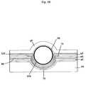
- a light-emitting panelis made from two substrates, wherein one of the substrates includes a plurality of sockets and wherein at least two electrodes are disposed. At least partially disposed in each socket is a micro-component, although more than one micro-component may be disposed therein. Each micro-component includes a shell at least partially filled with a gas or gas mixture capable of ionization. When a large enough voltage is applied across the micro-component the gas or gas mixture ionizes forming plasma and emitting radiation.
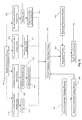
- a method for inline testing a plurality of light-emitting panelsincludes manufacturing a plurality of light-emitting panels in a web fabrication process that includes a plurality of process steps and component parts, testing a portion of one or more light-emitting panels after at least one process step is performed at least one time, processing data from the testing to produce at least one result; analyzing the results to determine whether the result is within acceptable tolerances and adjusting at least one of the process steps or at least one component part is the results are not within acceptable tolerances.
- a method for forming a light-emitting panelincludes providing a first substrate, forming a plurality of cavities on or within the first substrate, placing at least one micro-component in each cavity, providing a second substrate opposed to the first substrate such that at least one micro-component is sandwiched between the first and second substrates, disposing at least two electrodes so that voltage supplied to the at least two electrodes causes one or more micro-components to emit radiation; and inline testing at least one of the first substrate, at least one cavity, at least one micro-component, at least one electrode, and the second substrate.
- FIG. 1depicts a portion of a light-emitting panel showing the basic socket structure of a socket formed from patterning a substrate, as disclosed in an embodiment of the present invention.
- FIG. 2depicts a portion of a light-emitting panel showing the basic socket structure of a socket formed from patterning a substrate, as disclosed in another embodiment of the present invention.
- FIG. 3Ashows an example of a cavity that has a cube shape.
- FIG. 3Bshows an example of a cavity that has a cone shape.
- FIG. 3Cshows an example of a cavity that has a conical frustum shape.
- FIG. 3Dshows an example of a cavity that has a paraboloid shape.
- FIG. 3Eshows an example of a cavity that has a spherical shape.
- FIG. 3Fshows an example of a cavity that has a cylindrical shape.
- FIG. 3Gshows an example of a cavity that has a pyramid shape.
- FIG. 3Hshows an example of a cavity that has a pyramidal frustum shape.
- FIG. 3Ishows an example of a cavity that has a parallelepiped shape.
- FIG. 3Jshows an example of a cavity that has a prism shape.
- FIG. 4shows the socket structure from a light-emitting panel of an embodiment of the present invention with a narrower field of view.
- FIG. 5shows the socket structure from a light-emitting panel of an embodiment of the present invention with a wider field of view.
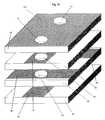
- FIG. 6Adepicts a portion of a light-emitting panel showing the basic socket structure of a socket formed from disposing a plurality of material layers and then selectively removing a portion of the material layers with the electrodes having a co-planar configuration.
- FIG. 6Bis a cut-away of FIG. 6A showing in more detail the co-planar sustaining electrodes.
- FIG. 7Adepicts a portion of a light-emitting panel showing the basic socket structure of a socket formed from disposing a plurality of material layers and then selectively removing a portion of the material layers with the electrodes having a mid-plane configuration.
- FIG. 7Bis a cut-away of FIG. 7A showing in more detail the uppermost sustain electrode.
- FIG. 8depicts a portion of a light-emitting panel showing the basic socket structure of a socket formed from disposing a plurality of material layers and then selectively removing a portion of the material layers with the electrodes having an configuration with two sustain and two address electrodes, where the address electrodes are between the two sustain electrodes.
- FIG. 9depicts a portion of a light-emitting panel showing the basic socket structure of a socket formed from patterning a substrate and then disposing a plurality of material layers on the substrate so that the material layers conform to the shape of the cavity with the electrodes having a co-planar configuration.
- FIG. 10depicts a portion of a light-emitting panel showing the basic socket structure of a socket formed from patterning a substrate and then disposing a plurality of material layers on the substrate so that the material layers conform to the shape of the cavity with the electrodes having a mid-plane configuration.
- FIG. 11depicts a portion of a light-emitting panel showing the basic socket structure of a socket formed from patterning a substrate and then disposing a plurality of material layers on the substrate so that the material layers conform to the shape of the cavity with the electrodes having an configuration with two sustain and two address electrodes, where the address electrodes are between the two sustain electrodes.
- FIG. 12is a flowchart describing a web fabrication method for manufacturing light-emitting panels and depicting various points throughout the method at which testing would take place as described in an embodiment of the present invention.
- FIG. 13is an example of data taken and stored after one of the fabrication process steps as described in an embodiment of the present invention.
- FIG. 14shows an exploded view of a portion of a light-emitting panel showing the basic socket structure of a socket formed by disposing a plurality of material layers with aligned apertures on a substrate with the electrodes having a co-planar configuration.
- FIG. 15shows an exploded view of a portion of a light-emitting panel showing the basic socket structure of a socket formed by disposing a plurality of material layers with aligned apertures on a substrate with the electrodes having a mid-plane configuration.
- FIG. 16shows an exploded view of a portion of a light-emitting panel showing the basic socket structure of a socket formed by disposing a plurality of material layers with aligned apertures on a substrate with electrodes having a configuration with two sustain and two address electrodes, where the address electrodes are between the two sustain electrodes.
- the preferred embodiments of the present inventionare directed to a novel light-emitting panel.
- preferred embodimentsare directed to light-emitting panels and a method for testing light-emitting panels and the components therein.
- FIGS. 1 and 2show two embodiments of the present invention wherein a light-emitting panel includes a first substrate 10 and a second substrate 20 .
- the first substrate 10may be made from silicates, polypropylene, quartz, glass, any polymeric-based material or any material or combination of materials known to one skilled in the art.
- second substrate 20may be made from silicates, polypropylene, quartz, glass, any polymeric-based material or any material or combination of materials known to one skilled in the art.
- First substrate 10 and second substrate 20may both be made from the same material or each of a different material.
- the first and second substratemay be made of a material that dissipates heat from the light-emitting panel.
- each substrateis made from a material that is mechanically flexible.
- the first substrate 10includes a plurality of sockets 30 .
- the sockets 30may be disposed in any pattern, having uniform or non-uniform spacing between adjacent sockets. Patterns may include, but are not limited to, alphanumeric characters, symbols, icons, or pictures.
- the sockets 30are disposed in the first substrate 10 so that the distance between adjacent sockets 30 is approximately equal.
- Sockets 30may also be disposed in groups such that the distance between one group of sockets and another group of sockets is approximately equal. This latter approach may be particularly relevant in color light-emitting panels, where each socket in each group of sockets may represent red, green and blue, respectively.
- each socket 30At least partially disposed in each socket 30 is at least one micro-component 40 .
- Multiple micro-componentsmay be disposed in a socket to provide increased luminosity and enhanced radiation transport efficiency.
- a single socketsupports three micro-components configured to emit red, green, and blue light, respectively.
- the micro-components 40may be of any shape, including, but not limited to, spherical, cylindrical, and aspherical.
- a micro-component 40includes a micro-component placed or formed inside another structure, such as placing a spherical micro-component inside a cylindrical-shaped structure.
- each cylindrical-shaped structureholds micro-components configured to emit a single color of visible light or multiple colors arranged red, green, blue, or in some other suitable color arrangement.
- an adhesive or bonding agentis applied to each micro-component to assist in placing/holding a micro-component 40 or plurality of micro-components in a socket 30 .
- an electrostatic chargeis placed on each micro-component and an electrostatic field is applied to each micro-component to assist in the placement of a micro-component 40 or plurality of micro-components in a socket 30 . Applying an electrostatic charge to the micro-components also helps avoid agglomeration among the plurality of micro-components.
- an electron gunis used to place an electrostatic charge on each micro-component and one electrode disposed proximate to each socket 30 is energized to provide the needed electrostatic field required to attract the electrostatically charged micro-component.
- a socket 30may contain a bonding agent or an adhesive.
- the bonding agent or adhesivemay be applied to the inside of the socket 30 by differential stripping, lithographic process, sputtering, laser deposition, chemical deposition, vapor deposition, or deposition using ink jet technology.
- differential strippinglithographic process, sputtering, laser deposition, chemical deposition, vapor deposition, or deposition using ink jet technology.
- each micro-component 40includes a shell 50 filled with a plasma-forming gas or gas mixture 45 .
- a plasma-forming gas or gas mixture 45Any suitable gas or gas mixture 45 capable of ionization may be used as the plasma-forming gas, including, but not limited to, krypton, xenon, argon, neon, oxygen, helium, mercury, and mixtures -thereof.
- any noble gascould be used as the plasma-forming gas, including, but not limited to, noble gases mixed with cesium or mercury.
- One skilled in the artwould recognize other gasses or gas mixtures that could also be used.
- the plasma-forming gas or gas mixture 45is chosen so that during ionization the gas will irradiate a specific wavelength of light corresponding to a desired color.
- a plasma-forming gas or gas mixture 45is used in a preferred embodiment, any other material capable of providing luminescence is also contemplated, such as an electro-luminescent material, organic light-emitting diodes (OLEDs), or an electro-phoretic material.
- the shell 50may be made from a wide assortment of materials, including, but not limited to, silicates, polypropylene, glass, any polymeric-based material, magnesium oxide and quartz and may be of any suitable size.
- the shell 50may have a diameter ranging from micrometers to centimeters as measured across its minor axis, with virtually no limitation as to its size as measured across its major axis.
- a cylindrical-shaped micro-componentmay be only 100 microns in diameter across its minor axis, but may be hundreds of meters long across its major-axis.
- the outside diameter of the shell, as measured across its minor axisis from 100 microns to 300 microns.
- the shell thicknessmay range from micrometers to millimeters, with a preferred thickness from 1 micron to 10 microns.
- the gas or gas mixtureWhen a sufficiently large voltage is applied across the micro-component the gas or gas mixture ionizes forming plasma and emitting radiation.
- the potential required to initially ionize the gas or gas mixture inside the shell 50is governed by Paschen's Law and is closely related to the pressure of the gas inside the shell.
- the gas pressure inside the shell 50ranges from tens of torrs to several atmospheres. In a preferred embodiment, the gas pressure ranges from 100 torr to 700 torr.
- the size and shape of a micro-component 40 and the type and pressure of the plasma-forming gas contained therein,influence the performance and characteristics of the light-emitting panel and are selected to optimize the panel's efficiency of operation.
- coatings 300 and dopantsthat may be added to a micro-component 40 that also influence the performance and characteristics of the light-emitting panel.
- the coatings 300may be applied to the outside or inside of the shell 50 , and may either partially or fully coat the shell 50 .
- Types of outside coatingsinclude, but are not limited to, coatings used to convert UV light to visible light (e.g. phosphor), coatings used as reflecting filters, and coatings used as band-gap filters.
- Types of inside coatingsinclude, but are not limited to, coatings used to convert UV light to visible light (e.g. phosphor), coatings used to enhance secondary emissions and coatings used to prevent erosion.
- coatingsmay also be used.
- the coatings 300may be applied to the shell 50 by differential stripping, lithographic process, sputtering, laser deposition, chemical deposition, vapor deposition, or deposition using ink jet technology.
- One skilled in the artwill realize that other methods of coating the inside and/or outside of the shell 50 may be used.
- Types of dopantsinclude, but are not limited to, dopants used to convert UV light to visible light (e.g., phosphor), dopants used to enhance secondary emissions and dopants used to provide a conductive path through the shell 50 .
- the dopantsare added to the shell 50 by any suitable technique known to one skilled in the art, including ion implantation.
- any combination of coatings and dopantsmay be added to a micro-component 40 .
- a variety of coatings 350may be coated on the inside of a socket 30 .
- These coatings 350include, but are not limited to, coatings used to convert UV light to visible light, coatings used as reflecting filters, and coatings used as band-gap filters.
- the UV lightwhen a micro-component is configured to emit UV light, the UV light is converted to visible light by at least partially coating the inside the shell 50 with phosphor, at least partially coating the outside of the shell 50 with phosphor, doping the shell 50 with phosphor and/or coating the inside of a socket 30 with phosphor.
- colored phosphoris chosen so the visible light emitted from alternating micro-components is colored red, green and blue, respectively. By combining these primary colors at varying intensities, all colors can be formed. It is contemplated that other color combinations and arrangements may be used.
- the UV lightis converted to visible light by disposing a single colored phosphor on the micro-component 40 and/or on the inside of the socket 30 .
- Colored filtersmay then be alternatingly applied over each socket 30 to convert the visible light to colored light of any suitable arrangement, for example red, green and blue.
- the shell 50 of each micro-component 40is at least partially coated with a secondary emission enhancement material.
- a secondary emission enhancement materialAny low affinity material may be used including, but not limited to, magnesium oxide and thulium oxide.
- the shell 50is doped with a secondary emission enhancement material. It is contemplated that the doping of shell 50 with a secondary emission enhancement material may be in addition to coating the shell 50 with a secondary emission enhancement material. In this case, the secondary emission enhancement material used to coat the shell 50 and dope the shell 50 may be different.
- the shell 50is doped with a conductive material.
- conductive materialsinclude, but are not limited to silver, gold, platinum, and aluminum. Doping the shell 50 with a conductive material provides a direct conductive path to the gas or gas mixture contained in the shell and provides one possible means of achieving a DC light-emitting panel.
- the shell 50 of the micro-component 40is coated with a reflective material.
- An index matching material that matches the index of refraction of the reflective materialis disposed so as to be in contact with at least a portion of the reflective material.
- the reflective coating and index matching materialmay be separate from, or in conjunction with, the phosphor coating and secondary emission enhancement coating of previous embodiments.
- the reflective coatingis applied to the shell 50 in order to enhance radiation transport.
- the index matching materialis coated directly over at least a portion of the reflective coating.
- the index matching materialis disposed on a material layer, or the like, that is brought in contact with the micro-component such that the index matching material is in contact with at least a portion of the reflective coating.
- the size of the interfaceis selected to achieve a specific field of view for the light-emitting panel.
- a cavity 55 formed within and/or on the first substrate 10provides the basic socket 30 structure.
- the cavity 55may be any shape and size.
- the shape of the cavity 55may include, but is not limited to, a cube 100 , a cone 110 , a conical frustum 120 , a paraboloid 130 , spherical 140 , cylindrical 150 , a pyramid 160 , a pyramidal frustum 170 , a parallelepiped 180 , or a prism 190 .
- the size and shape of the socket 30influence the performance and characteristics of the light-emitting panel and are selected to optimize the panel's efficiency of operation.
- socket geometrymay be selected based on the shape and size of the micro-component to optimize the surface contact between the micro-component and the socket and/or to ensure connectivity of the micro-component and any electrodes disposed within the socket.
- the size and shape of the sockets 30may be chosen to optimize photon generation and provide increased luminosity and radiation transport efficiency. As shown by example in FIGS.
- the size and shapemay be chosen to provide a field of view 400 with a specific angle ⁇ , such that a micro-component 40 disposed in a deep socket 30 may provide more collimated light and hence a narrower viewing angle ⁇ (FIG. 4 ), while a micro-component 40 disposed in a shallow socket 30 may provide a wider viewing angle ⁇ (FIG. 5 ). That is to say, the cavity may be sized, for example, so that its depth subsumes a micro-component deposited in a socket, or it may be made shallow so that a micro-component is only partially disposed within a socket.
- the field of view 400may be set to a specific angle ⁇ by disposing on the second substrate at least one optical lens.
- the lensmay cover the entire second substrate or, in the case of multiple optical lenses, arranged so as to be in register with each socket.
- the optical lens or optical lensesare configurable to adjust the field of view of the light-emitting panel.
- a cavity 55is formed, or patterned, in a substrate 10 to create a basic socket shape.
- the cavitymay be formed in any suitable shape and size by any combination of physically, mechanically, thermally, electrically, optically, or chemically deforming the substrate.
- Disposed proximate to, and/or in, each socketmay be a variety of enhancement materials 325 .
- the enhancement materials 325include, but are not limited to, anti-glare coatings, touch sensitive surfaces, contrast enhancement coatings, protective coatings, transistors, integrated-circuits, semiconductor devices, inductors, capacitors, resistors, control electronics, drive electronics, diodes, pulse-forming networks, pulse compressors, pulse transformers, and tuned-circuits.
- a socket 30is formed by disposing a plurality of material layers 60 to form a first substrate 10 , disposing at least one electrode either directly on the first substrate 10 , within the material layers or any combination thereof, and selectively removing a portion of the material layers 60 to create a cavity.
- the material layers 60include any combination, in whole or in part, of dielectric materials, metals, and enhancement materials 325 .
- the enhancement materials 325include, but are not limited to, anti-glare coatings, touch sensitive surfaces, contrast enhancement coatings, protective coatings, transistors, integrated-circuits, semiconductor devices, inductors, capacitors, resistors, control electronics, drive electronics, diodes, pulse-forming networks, pulse compressors, pulse transformers, and tuned-circuits.
- the placement of the material layers 60may be accomplished by any transfer process, photolithography, sputtering, laser deposition, chemical deposition, vapor deposition, or deposition using ink jet technology.
- One of general skill in the artwill recognize other appropriate methods of disposing a plurality of material layers on a substrate.
- the cavity 55may be formed in the material layers 60 by a variety of methods including, but not limited to, wet or dry etching, photolithography, laser heat treatment, thermal form, mechanical punch, embossing, stamping-out, drilling, electroforming or by dimpling.
- a socket 30is formed by patterning a cavity 55 in a first substrate 10 , disposing a plurality of material layers 65 on the first substrate 10 so that the material layers 65 conform to the cavity 55 , and disposing at least one electrode on the first substrate 10 , within the material layers 65 , or any combination thereof.
- the cavitymay be formed in any suitable shape and size by any combination of physically, mechanically, thermally, electrically, optically, or chemically deforming the substrate.
- the material layers 60include any combination, in whole or in part, of dielectric materials, metals, and enhancement materials 325 .
- the enhancement materials 325include, but are not limited to, anti-glare coatings, touch sensitive surfaces, contrast enhancement coatings, protective coatings, transistors, integrated-circuits, semiconductor devices, inductors, capacitors, resistors, control electronics, drive electronics, diodes, pulse-forming networks, pulse compressors, pulse transformers, and tuned-circuits.
- the placement of the material layers 60may be accomplished by any transfer process, photolithography, sputtering, laser deposition, chemical deposition, vapor deposition, or deposition using ink jet technology.
- One of general skill in the artwill recognize other appropriate methods of disposing a plurality of material layers on a substrate.
- a socket 30is formed by disposing a plurality of material layers 66 on a first substrate 10 and disposing at least one electrode on the first substrate 10 , within the material layers 66 ,-or any combination thereof.
- Each of the material layersincludes a preformed aperture 56 that extends through the entire material layer.
- the aperturesmay be of the same size or may be of different sizes.
- The. plurality of material layers 66are disposed on the first substrate with the apertures in alignment thereby forming a cavity 55 .
- the material layers 66include any combination, in whole or in part, of dielectric materials, metals, and enhancement materials 325 .
- the enhancement materials 325include, but are not limited to, anti-glare coatings, touch sensitive surfaces, contrast enhancement coatings, protective coatings, transistors, integrated-circuits, semiconductor devices, inductors, capacitors, resistors, diodes, control electronics, drive electronics, pulse-forming networks, pulse compressors, pulse transformers, and tuned-circuits.
- the placement of the material layers 66may be accomplished by any transfer process, photolithography, sputtering, laser deposition, chemical deposition, vapor-deposition, or deposition using ink jet technology.
- One of general skill in the artwill recognize other appropriate methods of disposing a plurality of material layers on a substrate.
- each socketmay be at least one enhancement material.
- the enhancement material 325may include, but is not limited to, anti-glare coatings, touch sensitive surfaces, contrast enhancement coatings, protective coatings, transistors, integrated-circuits, semiconductor devices, inductors, capacitors, resistors, control electronics, drive electronics, diodes, pulse-forming networks, pulse compressors, pulse transformers, and tuned-circuits.
- the enhancement materialsmay be disposed in, or proximate to each socket by any transfer process, photolithography, sputtering, laser deposition, chemical deposition, vapor deposition, deposition using ink jet technology, or mechanical means.
- a method for making a light-emitting panelincludes disposing at least one electrical enhancement (e.g. the transistors, integrated-circuits, semiconductor devices, inductors, capacitors, resistors, control electronics, drive electronics, diodes, pulse-forming networks, pulse compressors, pulse transformers, and tuned-circuits), in, or proximate to, each socket by suspending the at least one electrical enhancement in a liquid and flowing the liquid across the first substrate.
- at least one electrical enhancemente.g. the transistors, integrated-circuits, semiconductor devices, inductors, capacitors, resistors, control electronics, drive electronics, diodes, pulse-forming networks, pulse compressors, pulse transformers, and tuned-circuits
- the at least one electrical enhancementwill settle in each socket. It is contemplated that other substances or means may be use to move the electrical enhancements across the substrate. One such means may include, but is not limited to, using air to move the electrical enhancements across the substrate.
- the socketis of a corresponding shape to the at least one electrical enhancement such that the at least one electrical enhancement self-aligns with the socket.
- the electrical enhancementsmay be used in a light-emitting panel for a number of purposes including, but not limited to, lowering the voltage necessary to ionize the plasma-forming gas in a micro-component, lowering the voltage required to sustain/erase the ionization charge in a micro-component, increasing the luminosity and/or radiation transport efficiency of a micro-component, and augmenting the frequency at which a micro-component is lit.
- the electrical enhancementsmay be used in conjunction with the light-emitting panel driving circuitry to alter the power requirements necessary to drive the light-emitting panel.
- a tuned-circuitmay be used in conjunction with the driving circuitry to allow a DC power source to power an AC-type light-emitting panel.
- a controlleris provided that is connected to the electrical enhancements and capable of controlling their operation. Having the ability to individual control the electrical enhancements at each pixel/subpixel provides a means by which the characteristics of individual micro-components may be altered/corrected after fabrication of the light-emitting panel. These characteristics include, but are not limited to, luminosity and the frequency at which a micro-component is lit.
- electrical enhancementsdisposed in, or proximate to, each socket in a light-emitting panel.
- the electrical potential necessary to energize a micro-component 40is supplied via at least two electrodes.
- the electrodesmay be disposed in the light-emitting panel using any technique know to one skilled in the art including, but not limited to, any transfer process, photolithography, sputtering, laser deposition, chemical deposition, vapor deposition, deposition using ink jet technology, or mechanical means.
- a light-emitting panelincludes a plurality of electrodes, wherein at least two electrodes are adhered to the first substrate, the second substrate or any combination thereof and wherein the electrodes are arranged so that voltage applied to the electrodes causes one or more micro-components to emit radiation.
- a light-emitting panelin another general embodiment, includes a plurality of electrodes, wherein at least two electrodes are arranged so that voltage supplied to the electrodes cause one or more micro-components to emit radiation throughout the field of view of the light-emitting panel without crossing either of the electrodes.
- At least two electrodesmay be disposed on the first substrate 10 , the second substrate 20 , or any combination thereof.
- a sustain electrode 70is adhered on the second substrate 20 and an address electrode 80 is adhered on the first substrate 10 .
- at least one electrode adhered to the first substrate 10is at least partly disposed within the socket (FIGS. 1 and 2 ).
- first substrate 10includes a plurality of material layers 60 and the sockets 30 are formed within the material layers
- at least two electrodesmay be disposed on the first substrate 10 , disposed within the material layers 60 , disposed on the second substrate 20 , or any combination thereof.
- a first address electrode 80is disposed within the material layers 60
- a first sustain electrode 70is disposed within the material layers 60
- a second sustain electrode 75is disposed within the material layers 60 , such that the first sustain electrode and the second sustain electrode are in a co-planar configuration.
- FIG. 6Bis a cut-away of FIG. 6A showing the arrangement of the co-planar sustain electrodes 70 and 75 .
- FIG. 6Ais a cut-away of FIG. 6A showing the arrangement of the co-planar sustain electrodes 70 and 75 .
- FIG. 7Aa first sustain electrode 70 is disposed on the first substrate 10 , a first address electrode 80 is disposed within the material layers 60 , and a second sustain electrode 75 is disposed within the material layers 60 , such that the first address electrode is located between the first sustain electrode and the second sustain electrode in a mid-plane configuration.
- FIG. 7Bis a cut-away of FIG. 7A showing the first sustain electrode 70 . As seen in FIG.
- a first sustain electrode 70is disposed within the material layers 60
- a first address electrode 80is disposed within the material layers 60
- a second address electrode 85is disposed within the material layers 60
- a second sustain electrode 75is disposed within the material layers 60 , such that the first address electrode and the second address electrode are located between the first sustain electrode and the second sustain electrode.
- At least two electrodesmay be disposed on the first substrate 10 , at least partially disposed within the material layers 65 , disposed on the second substrate 20 , or any combination thereof.
- a first address electrode 80is disposed on the first substrate 10
- a first sustain electrode 70is disposed within the material layers 65
- a second sustain electrode 75is disposed within the material layers 65 , such that the first sustain electrode and the second sustain electrode are in a co-planar configuration.
- a first sustain electrode 70is disposed on the first substrate 10
- a first address electrode 80is disposed within the material layers 65
- a second sustain electrode 75is disposed within the material layers 65 , such that the first address electrode is located between the first sustain electrode and the second sustain electrode in a mid-plane configuration.
- a first sustain electrode 70is disposed on the first substrate 10
- a first address electrode 80is disposed within the material layers 65
- a second address electrode 85is disposed within the material layers 65
- a second sustain electrode 75is disposed within the material layers 65 , such that the first address electrode and the second address electrode are located between the first sustain electrode and the second sustain electrode.
- At least two electrodesmay be disposed on the first substrate 10 , at least partially disposed within the material layers 65 , disposed on the second substrate 20 , or any combination thereof.
- a first address electrode 80is disposed on the first substrate 10
- a first sustain electrode 70is disposed within the material layers 66
- a second sustain electrode 75is disposed within the material layers 66 , such that the first sustain electrode and the second sustain electrode are in a co-planar configuration.
- FIG. 14shows that the first sustain electrode and the second sustain electrode are in a co-planar configuration.
- a first sustain electrode 70is disposed on the first substrate 10
- a first address electrode 80is disposed within the material layers 66
- a second sustain electrode 75is disposed within the material layers 66 , such that the first address electrode is located between the first sustain electrode and the second sustain electrode in a mid-plane configuration.
- a first sustain electrode 70is disposed on the first substrate 10
- a first address electrode 80is disposed within the material layers 66
- a second address electrode 85is disposed within the material layers 66
- a second sustain electrode 75is disposed within the material layers 66 , such that the first address electrode and the second address electrode are located between the first sustain electrode and the second sustain electrode.
- a process for testing a plurality of light-emitting panelscomprises manufacturing a plurality of light-emitting panels in a web fabrication process.
- the web fabrication processincludes a series of process steps and a plurality of component parts, as described in this application.
- a portion of a light-emitting panelis tested after one or more of the process steps.
- Data from the testingis processed and the results are analyzed to determine whether the results are within a specific target range of acceptable values for the portion of the light-emitting panel being tested. If the results are within acceptable ranges then no action is taken. If, however, the results fall outside the target range, then the results are used to adjust at least one of the process steps of the web fabrication process to bring the fabrication process back within acceptable tolerances.
- testingbe performed at larger intervals. That is to say, by way of a non-limiting example, that it is contemplated that an electrode disposed as part of an electrode printing process may be tested either after each time the electrode printing process is performed or after every fifth time the electrode printing process is performed. It is also contemplated, in another embodiment of the present invention, that testing results may either be immediately used to adjust at least one process step of the manufacturing process and/or at least one component part of the light-emitting panel or the testing results may be stored.
- the testing resultsare analyzed to determine whether the results fall within a target range of acceptable values. If the results are acceptable no action is taken, however, if the results fall outside the target range, at least one process step and/or at least one component part is adjusted according to the results to bring the manufacturing process back within acceptable tolerances. In the latter case, the stored testing results are analyzed to determine whether a pattern of consistent non-conformity exists.
- FIG. 13shows an example of data taken after the micro-component forming process regarding the thickness of the micro-component shell. The data was taken after each micro-component forming process operation and stored.
- FIG. 13shows the upper target limit 550 , the lower target limit 560 and the target value 570 .
- a web fabrication process for manufacturing light-emitting panelsincludes the following process steps: a micro-component forming process 900 ; a socket formation process 910 ; an electrode placement process 920 ; a micro-component placement process 930 ; an alignment process 940 ; and a panel dicing process 950 . It should be made clear that the process steps may be performed in any suitable order.
- process stepsmay be performed in conjunction with other process steps such that two or more process steps are performed simultaneously. Furthermore, it is contemplated that two or more process steps may be combined into a single process step.
- a testing method used to test a characteristic of a component partmay be used regardless of the what component part is being tested. That is to say, unless otherwise noted, that the testing method is related to the characteristic being tested not the component part. Therefore, unless otherwise noted, testing methods for similar characteristics will not be repeatedly discussed.
- the micro-component forming process 900at least one micro-component is formed and at least partially filled with a plasma-producing gas.
- the micro-component forming process 900also includes a micro-component coating process 905 .
- the micro-component coating process 905may occur at any suitable place during or after the micro-component forming process 900 .
- inline testingis performed on at least one micro-component.
- the characteristics of the one or more micro-components that may be testedinclude, but are not limited to, size, shape, impedance, gas composition and pressure, and shell thickness.
- the size of the micro-componentmay be tested using image capture, process, and analysis, laser acoustic analysis, expert system analysis or another method known to one of skill in the art.
- the shape of the micro-componentmay be tested using image capture, process and analysis, or another method known to one of skill in the art.
- the impedance of the micro-component, in the case where the micro-component shell is doped with a conductive material,may be tested using microwave excitation or another method known to one of skill in the art.
- the gas composition and pressure of the micro-componentmay be tested using microwave excitation and intensity measurements, ultraviolet spectral analysis or another method known to one of skill in the art.
- the shell thickness of the micro-componentmay be tested interferometricly, using laser analysis or using another method known to one of skill in the art. It is contemplated, in an embodiment, that preformed micro-components with/without coatings may be used in the web fabrication process thereby alleviating the need for a micro-component forming process 900 or micro-component coating process 905 .
- a plurality of sockets 30are formed within or on a first substrate 10 .
- the socket formation process 910includes an electrode and enhancement material placement process 912 and a patterning process 914 .
- the socket formation process 910includes an electrode and enhancement material placement process 912 , a material layer placement process 916 , and a material layer removal process 918 .
- the socket formation process 910includes an electrode and enhancement material placement process 912 , a patterning process 914 , and-a material layer placement and conforming process 919 .
- the socket formation process 910includes an electrode and enhancement material placement process 912 and a material layer placement and alignment process 917 .
- inline testingis performed on at least one socket. It is contemplated that since each embodiment of the socket formation process 910 includes a plurality of process steps that the inline testing may be performed after each of the process steps as opposed to inline testing after the socket is completely formed.
- inline testingis performed on at least one electrode and/or at least one enhancement material.
- the characteristics of the one or more electrodes and/or the one or more enhancement materials that may be testedinclude, but are not limited to, placement, impedance, size, shape, material properties and enhancement material functionality. The placement of the electrode and/or enhancement material may be tested using image capture, process and analysis or another method known to one of skill in the art.
- the impedance of the electrode and/or enhancement materialwhen applicable, may be tested using standard time domain analysis or another method known to one of skill in the art.
- the material properties of the electrode and/or enhancement materialmay be tested using light transmission and intensity measurements, expert system analysis, image capture, process and analysis, laser acoustic analysis or another method known to one of skill in the art.
- inline testingis performed on at least one cavity.
- the characteristics of the one or more cavities that may be testedinclude, but are not limited to, placement, impedance, size, shape, depth, wall quality and edge quality.
- the depth of the cavitymay be tested using image capture, process and analysis, laser scanning and profiling, position-spatial frequency or another method known to one of skill in the art.
- inline testingis performed on at least one material layer.
- the characteristics of the one or more material layers that may be testedinclude, but are not limited to, size, shape, thickness and material properties.
- inline testingis preformed on at least one cavity formed in the plurality of material layers as a result of the material layer removal process.
- the characteristics of the one or more cavitiesincludes, but is not limited to, size, shape, depth, wall quality and edge quality.
- inline testingis performed on at least one material layer.
- the characteristics of the one or more material layers that may be testedinclude, but are not limited to, size, shape, thickness and material properties.
- At least one electrode and/or driving or control circuitryis disposed on or within the first substrate, on the second substrate, or any combination thereof. It is contemplated that the electrode placement process 920 may be performed as part of the electrode and enhancement material placement process 912 when an electrode is disposed on or within the first substrate or may be performed as a separate step when an electrode is disposed on the second substrate. After the electrode placement process 920 , inline testing is performed on at least one electrode. The characteristics of the one or more electrodes that may be tested include, but are not limited to, placement, impedance, size, shape, material properties and electrical component functionality.
- micro-component placement process 930at least one micro-component is at least partially disposed in each socket.
- inline testingis performed on at least one micro-component.
- the characteristics of the one or more micro-components that may be testedinclude, but are not limited to, position and orientation.
- the position of the micro-componentmay be tested using image capture, process and analysis, expert system analysis, spatial frequency analysis or anther method known to one of skill in the art.
- the orientation of the micro-componentmay be tested using image capture, process and analysis, expert system analysis, or another method known to one of skill in the art.
- the additional characteristic of whether a proper color micro-component is placed in the proper socketmay also be tested by using ultraviolet excitation and visible color imaging or another method known to one of skill in the art.
- a second substrate 20is positioned and placed, directly or indirectly, on the first substrate 10 so that one or more micro-components are sandwiched between the first and second substrates.
- inline testingis performed on the second substrate.
- the characteristics of the second substrate that may be testedinclude, but are not limited to, position and orientation.
- the first and second “sandwiched” substratesare diced to form an individual light-emitting panel.
- inline testingis performed on the individual light-emitting panel.
- the characteristics of the individual light-emitting panel that may be testedinclude, but are not limited to, size, shape and luminosity.
- the luminosity, in both visible and non-visible regions, of the light-emitting displaymay be tested by pixel by pixel image analysis.
- the method of testing a light-emitting panelincludes manufacturing a light-emitting panel in a series of process steps, testing at least one component part of the light-emitting panel after at least one process step, analyzing the test data to produce at least one result and utilizing the at least one result to adjust one or more component parts of the light-emitting panel. It is contemplated in this embodiment, however, that the adjustment may be zero (i.e. no adjustment) if the results show that the fabrication process is within specified tolerances.
- the series of process stepsincludes providing a first substrate, forming a plurality of cavities on or within the first substrate, placing at least one micro-component at least partially in each cavity, providing a second substrate opposed to the first substrate such that the at least one micro-component is sandwiched between the first and second substrates, disposing at least two electrodes so that voltage applied to the electrodes causes one or more micro-components to emit radiation. Testing may be performed on the first substrate, at least one cavity, at least one micro-component, at least one electrode, and/or the second substrate.
- Adjustments, after testing and analysis,may be made to the first substrate, the formation of the first substrate, the formation of the plurality of cavities, the plurality of cavities, the at least one micro-component, the disposition of at least one of the at least two electrodes, one or more electrodes, the placement of the second substrate and/or the second substrate.
Landscapes
- Engineering & Computer Science (AREA)
- Manufacturing & Machinery (AREA)
- Physics & Mathematics (AREA)
- Plasma & Fusion (AREA)
- Electroluminescent Light Sources (AREA)
- Gas-Filled Discharge Tubes (AREA)
- Luminescent Compositions (AREA)
- Testing Of Optical Devices Or Fibers (AREA)
- Manufacture Of Electron Tubes, Discharge Lamp Vessels, Lead-In Wires, And The Like (AREA)
- Formation Of Various Coating Films On Cathode Ray Tubes And Lamps (AREA)
Abstract
Description
Claims (29)
Priority Applications (9)
| Application Number | Priority Date | Filing Date | Title |
|---|---|---|---|
| US09/697,498US6620012B1 (en) | 2000-10-27 | 2000-10-27 | Method for testing a light-emitting panel and the components therein |
| PCT/US2001/042782WO2002035510A1 (en) | 2000-10-27 | 2001-10-26 | A method for testing a light-emitting panel and the components therein |
| EP01988926AEP1332486A1 (en) | 2000-10-27 | 2001-10-26 | A method for testing a light-emitting panel and the components therein |
| KR10-2003-7005730AKR20030074612A (en) | 2000-10-27 | 2001-10-26 | A method for testing a light-emitting panel and the components therein |
| AU2002232386AAU2002232386A1 (en) | 2000-10-27 | 2001-10-26 | A method for testing a light-emitting panel and the components therein |
| JP2002538414AJP2004531690A (en) | 2000-10-27 | 2001-10-26 | Light-emitting panel and method of inspecting its components |
| CNA018179789ACN1471702A (en) | 2000-10-27 | 2001-10-26 | A method for testinga light-emtiting panel and the components therein |
| US10/214,716US6935913B2 (en) | 2000-10-27 | 2002-08-09 | Method for on-line testing of a light emitting panel |
| US10/606,246US20040063373A1 (en) | 2000-10-27 | 2003-06-26 | Method for testing a light-emitting panel and the components therein |
Applications Claiming Priority (1)
| Application Number | Priority Date | Filing Date | Title |
|---|---|---|---|
| US09/697,498US6620012B1 (en) | 2000-10-27 | 2000-10-27 | Method for testing a light-emitting panel and the components therein |
Related Child Applications (2)
| Application Number | Title | Priority Date | Filing Date |
|---|---|---|---|
| US10/214,716Continuation-In-PartUS6935913B2 (en) | 2000-10-27 | 2002-08-09 | Method for on-line testing of a light emitting panel |
| US10/606,246ContinuationUS20040063373A1 (en) | 2000-10-27 | 2003-06-26 | Method for testing a light-emitting panel and the components therein |
Publications (1)
| Publication Number | Publication Date |
|---|---|
| US6620012B1true US6620012B1 (en) | 2003-09-16 |
Family
ID=24801357
Family Applications (2)
| Application Number | Title | Priority Date | Filing Date |
|---|---|---|---|
| US09/697,498Expired - LifetimeUS6620012B1 (en) | 2000-10-27 | 2000-10-27 | Method for testing a light-emitting panel and the components therein |
| US10/606,246AbandonedUS20040063373A1 (en) | 2000-10-27 | 2003-06-26 | Method for testing a light-emitting panel and the components therein |
Family Applications After (1)
| Application Number | Title | Priority Date | Filing Date |
|---|---|---|---|
| US10/606,246AbandonedUS20040063373A1 (en) | 2000-10-27 | 2003-06-26 | Method for testing a light-emitting panel and the components therein |
Country Status (7)
| Country | Link |
|---|---|
| US (2) | US6620012B1 (en) |
| EP (1) | EP1332486A1 (en) |
| JP (1) | JP2004531690A (en) |
| KR (1) | KR20030074612A (en) |
| CN (1) | CN1471702A (en) |
| AU (1) | AU2002232386A1 (en) |
| WO (1) | WO2002035510A1 (en) |
Cited By (49)
| Publication number | Priority date | Publication date | Assignee | Title |
|---|---|---|---|---|
| WO2004015661A3 (en)* | 2002-08-09 | 2004-07-01 | Science Applic Int Corp | Method for on-line testing of a light-emitting panel |
| US6796867B2 (en)* | 2000-10-27 | 2004-09-28 | Science Applications International Corporation | Use of printing and other technology for micro-component placement |
| US20050130547A1 (en)* | 2003-12-12 | 2005-06-16 | Pioneer Plasma Display Corporation | Method of manufacturing plasma display panel and method of manufacturing plasma display apparatus |
| US7122961B1 (en) | 2002-05-21 | 2006-10-17 | Imaging Systems Technology | Positive column tubular PDP |
| US7157854B1 (en) | 2002-05-21 | 2007-01-02 | Imaging Systems Technology | Tubular PDP |
| US7288014B1 (en)* | 2000-10-27 | 2007-10-30 | Science Applications International Corporation | Design, fabrication, testing, and conditioning of micro-components for use in a light-emitting panel |
| US7405516B1 (en) | 2004-04-26 | 2008-07-29 | Imaging Systems Technology | Plasma-shell PDP with organic luminescent substance |
| US20080315109A1 (en)* | 2007-06-19 | 2008-12-25 | Stephan Andrew C | Neutron detector |
| US20080315108A1 (en)* | 2007-06-19 | 2008-12-25 | Stephan Andrew C | Neutron detector |
| US7535175B1 (en) | 2006-02-16 | 2009-05-19 | Imaging Systems Technology | Electrode configurations for plasma-dome PDP |
| US7595774B1 (en) | 1999-04-26 | 2009-09-29 | Imaging Systems Technology | Simultaneous address and sustain of plasma-shell display |
| US7604523B1 (en) | 2004-06-21 | 2009-10-20 | Imaging Systems Technology | Plasma-shell PDP |
| US7619591B1 (en) | 1999-04-26 | 2009-11-17 | Imaging Systems Technology | Addressing and sustaining of plasma display with plasma-shells |
| US7622866B1 (en) | 2005-02-22 | 2009-11-24 | Imaging Systems Technology | Plasma-dome PDP |
| US7628666B1 (en) | 2002-05-21 | 2009-12-08 | Imaging Systems Technology | Process for manufacturing plasma-dome PDP |
| US7638943B1 (en) | 2002-05-21 | 2009-12-29 | Imaging Systems Technology | Plasma-disc article of manufacture |
| US20100019164A1 (en)* | 2007-06-19 | 2010-01-28 | Stephan Andrew C | Neutron detector |
| US7679286B1 (en) | 2002-05-21 | 2010-03-16 | Imaging Systems Technology | Positive column tubular PDP |
| US7727040B1 (en) | 2002-05-21 | 2010-06-01 | Imaging Systems Technology | Process for manufacturing plasma-disc PDP |
| US7730746B1 (en) | 2005-07-14 | 2010-06-08 | Imaging Systems Technology | Apparatus to prepare discrete hollow microsphere droplets |
| US20100155617A1 (en)* | 2007-06-19 | 2010-06-24 | Stephan Andrew C | Neutron detector |
| US7772774B1 (en) | 2002-05-21 | 2010-08-10 | Imaging Systems Technology | Positive column plasma display tubular device |
| US7772773B1 (en) | 2003-11-13 | 2010-08-10 | Imaging Systems Technology | Electrode configurations for plasma-dome PDP |
| US7791037B1 (en) | 2006-03-16 | 2010-09-07 | Imaging Systems Technology | Plasma-tube radiation detector |
| US7863815B1 (en) | 2006-01-26 | 2011-01-04 | Imaging Systems Technology | Electrode configurations for plasma-disc PDP |
| US7923930B1 (en) | 2000-01-12 | 2011-04-12 | Imaging Systems Technology | Plasma-shell device |
| US7932674B1 (en) | 2002-05-21 | 2011-04-26 | Imaging Systems Technology | Plasma-dome article of manufacture |
| US7969092B1 (en) | 2000-01-12 | 2011-06-28 | Imaging Systems Technology, Inc. | Gas discharge display |
| US8035303B1 (en) | 2006-02-16 | 2011-10-11 | Imaging Systems Technology | Electrode configurations for gas discharge device |
| US8106586B1 (en) | 2004-04-26 | 2012-01-31 | Imaging Systems Technology, Inc. | Plasma discharge display with fluorescent conversion material |
| US8110987B1 (en) | 2002-05-21 | 2012-02-07 | Imaging Systems Technology, Inc. | Microshell plasma display |
| US8113898B1 (en) | 2004-06-21 | 2012-02-14 | Imaging Systems Technology, Inc. | Gas discharge device with electrical conductive bonding material |
| US8129906B1 (en) | 2004-04-26 | 2012-03-06 | Imaging Systems Technology, Inc. | Lumino-shells |
| US8138673B1 (en)* | 2002-05-21 | 2012-03-20 | Imaging Systems Technology | Radiation shielding |
| US8198811B1 (en) | 2002-05-21 | 2012-06-12 | Imaging Systems Technology | Plasma-Disc PDP |
| US8198812B1 (en)* | 2002-05-21 | 2012-06-12 | Imaging Systems Technology | Gas filled detector shell with dipole antenna |
| US8232725B1 (en) | 2002-05-21 | 2012-07-31 | Imaging Systems Technology | Plasma-tube gas discharge device |
| US8278824B1 (en) | 2006-02-16 | 2012-10-02 | Imaging Systems Technology, Inc. | Gas discharge electrode configurations |
| US8299696B1 (en) | 2005-02-22 | 2012-10-30 | Imaging Systems Technology | Plasma-shell gas discharge device |
| US8339041B1 (en) | 2004-04-26 | 2012-12-25 | Imaging Systems Technology, Inc. | Plasma-shell gas discharge device with combined organic and inorganic luminescent substances |
| US8368303B1 (en) | 2004-06-21 | 2013-02-05 | Imaging Systems Technology, Inc. | Gas discharge device with electrical conductive bonding material |
| US8410695B1 (en) | 2006-02-16 | 2013-04-02 | Imaging Systems Technology | Gas discharge device incorporating gas-filled plasma-shell and method of manufacturing thereof |
| US8513887B1 (en) | 2002-05-21 | 2013-08-20 | Imaging Systems Technology, Inc. | Plasma-dome article of manufacture |
| US8618733B1 (en) | 2006-01-26 | 2013-12-31 | Imaging Systems Technology, Inc. | Electrode configurations for plasma-shell gas discharge device |
| US8951608B1 (en) | 2004-10-22 | 2015-02-10 | Imaging Systems Technology, Inc. | Aqueous manufacturing process and article |
| US9013102B1 (en) | 2009-05-23 | 2015-04-21 | Imaging Systems Technology, Inc. | Radiation detector with tiled substrates |
| US9229937B2 (en) | 2006-04-06 | 2016-01-05 | Samsung Electronics Co., Ltd. | Apparatus and method for managing digital contents distributed over network |
| US9281153B1 (en)* | 2008-11-22 | 2016-03-08 | Imaging Systems Technology, Inc. | Gas filled detector shell |
| US20180100780A1 (en)* | 2016-10-12 | 2018-04-12 | Wal-Mart Stores, Inc. | Systems, Devices, and Methods for Detecting Spills |
Families Citing this family (5)
| Publication number | Priority date | Publication date | Assignee | Title |
|---|---|---|---|---|
| US6822626B2 (en)* | 2000-10-27 | 2004-11-23 | Science Applications International Corporation | Design, fabrication, testing, and conditioning of micro-components for use in a light-emitting panel |
| US6764367B2 (en)* | 2000-10-27 | 2004-07-20 | Science Applications International Corporation | Liquid manufacturing processes for panel layer fabrication |
| US20090309623A1 (en)* | 2008-06-11 | 2009-12-17 | Amethyst Research, Inc. | Method for Assessment of Material Defects |
| KR101578831B1 (en)* | 2014-06-02 | 2015-12-21 | 주식회사 코디에스 | Driving film for testing display panel and method for producing thereof |
| US10012520B2 (en) | 2014-12-01 | 2018-07-03 | Cooledge Lighting Inc. | Automated test systems and methods utilizing images to determine locations of non-functional light-emitting elements in light-emitting arrays |
Citations (123)
| Publication number | Priority date | Publication date | Assignee | Title |
|---|---|---|---|---|
| US3559190A (en) | 1966-01-18 | 1971-01-26 | Univ Illinois | Gaseous display and memory apparatus |
| US3646384A (en) | 1970-06-09 | 1972-02-29 | Ibm | One-sided plasma display panel |
| US3704052A (en) | 1971-05-03 | 1972-11-28 | Ncr Co | Method of making a plasma display panel |
| US3755027A (en) | 1970-11-19 | 1973-08-28 | Philips Corp | Method of manufacturing a gas discharge panel and panel manufactured by said method |
| US3848248A (en) | 1972-02-10 | 1974-11-12 | Sanders Associates Inc | Gaseous discharge device |
| US3969651A (en) | 1974-12-30 | 1976-07-13 | Ibm Corporation | Display system |
| US3990068A (en) | 1976-01-26 | 1976-11-02 | Control Data Corporation | Plasma display panel drive system |
| US3998618A (en) | 1975-11-17 | 1976-12-21 | Sanders Associates, Inc. | Method for making small gas-filled beads |
| US4027246A (en) | 1976-03-26 | 1977-05-31 | International Business Machines Corporation | Automated integrated circuit manufacturing system |
| US4035690A (en) | 1974-10-25 | 1977-07-12 | Raytheon Company | Plasma panel display device including spheroidal glass shells |
| US4303433A (en) | 1978-08-28 | 1981-12-01 | Torobin Leonard B | Centrifuge apparatus and method for producing hollow microspheres |
| US4393326A (en) | 1980-02-22 | 1983-07-12 | Okaya Electric Industries Co., Ltd. | DC Plasma display panel |
| US4429303A (en) | 1980-12-22 | 1984-01-31 | International Business Machines Corporation | Color plasma display device |
| US4534743A (en) | 1983-08-31 | 1985-08-13 | Timex Corporation | Process for making an electroluminescent lamp |
| US4554537A (en) | 1982-10-27 | 1985-11-19 | At&T Bell Laboratories | Gas plasma display |
| US4563617A (en)* | 1983-01-10 | 1986-01-07 | Davidson Allen S | Flat panel television/display |
| US4591847A (en) | 1969-12-15 | 1986-05-27 | International Business Machines Corporation | Method and apparatus for gas display panel |
| US4654561A (en) | 1985-10-07 | 1987-03-31 | Shelton Jay D | Plasma containment device |
| US4697123A (en) | 1980-11-19 | 1987-09-29 | Fujitsu Limited | Gas discharge panel |
| US4728864A (en) | 1986-03-03 | 1988-03-01 | American Telephone And Telegraph Company, At&T Bell Laboratories | AC plasma display |
| US4833463A (en) | 1986-09-26 | 1989-05-23 | American Telephone And Telegraph Company, At&T Bell Laboratories | Gas plasma display |
| US4843281A (en) | 1986-10-17 | 1989-06-27 | United Technologies Corporation | Gas plasma panel |
| US4887003A (en) | 1988-05-10 | 1989-12-12 | Parker William P | Screen printable luminous panel display device |
| US4912364A (en) | 1987-07-16 | 1990-03-27 | Tungsram Reszvenytarsasag | Three-phase high-pressure gas discharge lamp filled with a gas containing sodium or a metal-halide |
| US5019807A (en) | 1984-07-25 | 1991-05-28 | Staplevision, Inc. | Display screen |
| US5030888A (en) | 1988-08-26 | 1991-07-09 | Thomson-Csf | Very fast method of control by semi-selective and selective addressing of a coplanar sustaining AC type of plasma panel |
| US5062916A (en) | 1990-08-01 | 1991-11-05 | W. H. Brady Co. | Method for the manufacture of electrical membrane panels having circuits on flexible plastic films |
| US5068916A (en) | 1990-10-29 | 1991-11-26 | International Business Machines Corporation | Coordination of wireless medium among a plurality of base stations |
| US5075597A (en) | 1988-08-26 | 1991-12-24 | Thomson-Csf | Method for the row-by-row control of a coplanar sustaining ac type of plasma panel |
| US5126632A (en) | 1988-05-10 | 1992-06-30 | Parker William P | Luminous panel display device |
| US5150007A (en) | 1990-05-11 | 1992-09-22 | Bell Communications Research, Inc. | Non-phosphor full-color plasma display device |
| US5315129A (en) | 1990-08-20 | 1994-05-24 | University Of Southern California | Organic optoelectronic devices and methods |
| US5396149A (en) | 1991-09-28 | 1995-03-07 | Samsung Electron Devices Co., Ltd. | Color plasma display panel |
| US5500287A (en) | 1992-10-30 | 1996-03-19 | Innovation Associates, Inc. | Thermal insulating material and method of manufacturing same |
| US5510678A (en) | 1991-07-18 | 1996-04-23 | Nippon Hoso Kyokai | DC type gas-discharge display panel and gas-discharge display apparatus with employment of the same |
| US5514934A (en) | 1991-05-31 | 1996-05-07 | Mitsubishi Denki Kabushiki Kaisha | Discharge lamp, image display device using the same and discharge lamp producing method |
| US5674351A (en) | 1992-04-10 | 1997-10-07 | Candescent Technologies Corporation | Self supporting flat video display |
| US5675212A (en) | 1992-04-10 | 1997-10-07 | Candescent Technologies Corporation | Spacer structures for use in flat panel displays and methods for forming same |
| US5686790A (en) | 1993-06-22 | 1997-11-11 | Candescent Technologies Corporation | Flat panel device with ceramic backplate |
| US5703436A (en) | 1994-12-13 | 1997-12-30 | The Trustees Of Princeton University | Transparent contacts for organic devices |
| US5707745A (en) | 1994-12-13 | 1998-01-13 | The Trustees Of Princeton University | Multicolor organic light emitting devices |
| US5725787A (en) | 1992-04-10 | 1998-03-10 | Candescent Technologies Corporation | Fabrication of light-emitting device with raised black matrix for use in optical devices such as flat-panel cathode-ray tubes |
| US5746635A (en) | 1992-04-10 | 1998-05-05 | Candescent Technologies Corporation | Methods for fabricating a flat panel display having high voltage supports |
| US5747931A (en) | 1996-05-24 | 1998-05-05 | David Sarnoff Research Center, Inc. | Plasma display and method of making same |
| US5755944A (en) | 1996-06-07 | 1998-05-26 | Candescent Technologies Corporation | Formation of layer having openings produced by utilizing particles deposited under influence of electric field |
| US5757139A (en) | 1997-02-03 | 1998-05-26 | The Trustees Of Princeton University | Driving circuit for stacked organic light emitting devices |
| US5757131A (en) | 1995-08-11 | 1998-05-26 | Nec Corporation | Color plasma display panel and fabricating method |
| US5777782A (en) | 1996-12-24 | 1998-07-07 | Xerox Corporation | Auxiliary optics for a twisting ball display |
| US5788814A (en) | 1996-04-09 | 1998-08-04 | David Sarnoff Research Center | Chucks and methods for positioning multiple objects on a substrate |
| US5793158A (en) | 1992-08-21 | 1998-08-11 | Wedding, Sr.; Donald K. | Gas discharge (plasma) displays |
| US5808403A (en) | 1994-08-05 | 1998-09-15 | Pixel International S.A. | Microtip cathode with auxiliary insulating layer |
| US5811833A (en) | 1996-12-23 | 1998-09-22 | University Of So. Ca | Electron transporting and light emitting layers based on organic free radicals |
| US5815306A (en) | 1996-12-24 | 1998-09-29 | Xerox Corporation | "Eggcrate" substrate for a twisting ball display |
| US5837221A (en) | 1996-07-29 | 1998-11-17 | Acusphere, Inc. | Polymer-lipid microencapsulated gases for use as imaging agents |
| US5844363A (en) | 1997-01-23 | 1998-12-01 | The Trustees Of Princeton Univ. | Vacuum deposited, non-polymeric flexible organic light emitting devices |
| US5853446A (en) | 1996-04-16 | 1998-12-29 | Corning Incorporated | Method for forming glass rib structures |
| US5862054A (en)* | 1997-02-20 | 1999-01-19 | Taiwan Semiconductor Manufacturing Company, Ltd. | Process monitoring system for real time statistical process control |
| US5865657A (en) | 1996-06-07 | 1999-02-02 | Candescent Technologies Corporation | Fabrication of gated electron-emitting device utilizing distributed particles to form gate openings typically beveled and/or combined with lift-off or electrochemical removal of excess emitter material |
| US5897414A (en) | 1995-10-24 | 1999-04-27 | Candescent Technologies Corporation | Technique for increasing manufacturing yield of matrix-addressable device |
| US5898266A (en) | 1996-07-18 | 1999-04-27 | Candescent Technologies Corporation | Method for displaying frame of pixel information on flat panel display |
| US5914150A (en) | 1997-02-28 | 1999-06-22 | Candescent Technologies Corporation | Formation of polycarbonate film with apertures determined by etching charged-particle tracks |
| US5913704A (en) | 1993-09-08 | 1999-06-22 | Candescent Technologies Corporation | Fabrication of electronic devices by method that involves ion tracking |
| US5917646A (en) | 1996-12-24 | 1999-06-29 | Xerox Corporation | Rotatable lens transmissive twisting ball display |
| US5920080A (en) | 1997-06-23 | 1999-07-06 | Fed Corporation | Emissive display using organic light emitting diodes |
| US5945174A (en) | 1995-04-06 | 1999-08-31 | Delta V Technologies, Inc. | Acrylate polymer release coated sheet materials and method of production thereof |
| US5953587A (en) | 1997-11-24 | 1999-09-14 | The Trustees Of Princeton University | Method for deposition and patterning of organic thin film |
| US5965109A (en) | 1994-08-02 | 1999-10-12 | Molecular Biosystems, Inc. | Process for making insoluble gas-filled microspheres containing a liquid hydrophobic barrier |
| US5964630A (en) | 1996-12-23 | 1999-10-12 | Candescent Technologies Corporation | Method of increasing resistance of flat-panel device to bending, and associated getter-containing flat-panel device |
| US5969472A (en) | 1997-12-03 | 1999-10-19 | Lockheed Martin Energy Research Corporation | Lighting system of encapsulated luminous material |
| US5967871A (en) | 1997-07-24 | 1999-10-19 | Photonics Systems, Inc. | Method for making back glass substrate for plasma display panel |
| US5985460A (en) | 1994-12-05 | 1999-11-16 | E. I. Du Pont De Nemours And Company | Insulator composition, green tape, and method for forming plasma display apparatus barrier-rib |
| US5986409A (en) | 1998-03-30 | 1999-11-16 | Micron Technology, Inc. | Flat panel display and method of its manufacture |
| US5984747A (en) | 1996-03-28 | 1999-11-16 | Corning Incorporated | Glass structures for information displays |
| US5990614A (en) | 1998-02-27 | 1999-11-23 | Candescent Technologies Corporation | Flat-panel display having temperature-difference accommodating spacer system |
| US5990620A (en) | 1997-09-30 | 1999-11-23 | Lepselter; Martin P. | Pressurized plasma display |
| US6013538A (en) | 1997-11-24 | 2000-01-11 | The Trustees Of Princeton University | Method of fabricating and patterning OLEDs |
| US6017584A (en) | 1995-07-20 | 2000-01-25 | E Ink Corporation | Multi-color electrophoretic displays and materials for making the same |
| US6019657A (en) | 1997-09-17 | 2000-02-01 | Candescent Technologies Corporation | Dual-layer metal for flat panel display |
| US6022652A (en) | 1994-11-21 | 2000-02-08 | Candescent Technologies Corporation | High resolution flat panel phosphor screen with tall barriers |
| US6023259A (en) | 1997-07-11 | 2000-02-08 | Fed Corporation | OLED active matrix using a single transistor current mode pixel design |
| US6025097A (en) | 1997-02-28 | 2000-02-15 | Candescent Technologies Corporation | Method for creating a color filter layer on a field emission display screen structure |
| US6030715A (en) | 1997-10-09 | 2000-02-29 | The University Of Southern California | Azlactone-related dopants in the emissive layer of an OLED |
| US6030269A (en) | 1997-03-31 | 2000-02-29 | Candescent Technologies Corporation | Method for forming a multi-level conductive black matrix for a flat panel display |
| US6033547A (en) | 1996-11-26 | 2000-03-07 | The Trustees Of Princeton University | Apparatus for electrohydrodynamically assembling patterned colloidal structures |
| US6037710A (en) | 1998-04-29 | 2000-03-14 | Candescent Technologies, Inc. | Microwave sealing of flat panel displays |
| US6037918A (en) | 1998-03-30 | 2000-03-14 | Candescent Technologies, Inc. | Error compensator circuits used in color balancing with time multiplexed voltage signals for a flat panel display unit |
| US6038002A (en) | 1996-07-13 | 2000-03-14 | Lg Electronics Inc. | Thin film transistor liquid crystal display and method for fabricating the same |
| US6039619A (en) | 1997-05-22 | 2000-03-21 | Samsung Display Devices Co., Ltd. | Method and apparatus for manufacturing partition wall of plasma display device |
| US6045930A (en) | 1996-12-23 | 2000-04-04 | The Trustees Of Princeton University | Materials for multicolor light emitting diodes |
| US6046543A (en) | 1996-12-23 | 2000-04-04 | The Trustees Of Princeton University | High reliability, high efficiency, integratable organic light emitting devices and methods of producing same |
| US6049366A (en) | 1995-06-09 | 2000-04-11 | Sniaricerche S.C.P.A. | Polymer stabilized liquid crystals and flexible devices thereof |
| US6048630A (en) | 1996-07-02 | 2000-04-11 | The Trustees Of Princeton University | Red-emitting organic light emitting devices (OLED's) |
| US6069443A (en) | 1997-06-23 | 2000-05-30 | Fed Corporation | Passive matrix OLED display |
| US6072276A (en) | 1996-06-21 | 2000-06-06 | Nec Corporation | Color plasma display panel and method of manufacturing the same |
| US6080606A (en) | 1996-03-26 | 2000-06-27 | The Trustees Of Princeton University | Electrophotographic patterning of thin film circuits |
| US6087196A (en) | 1998-01-30 | 2000-07-11 | The Trustees Of Princeton University | Fabrication of organic semiconductor devices using ink jet printing |
| US6091195A (en) | 1997-02-03 | 2000-07-18 | The Trustees Of Princeton University | Displays having mesa pixel configuration |
| US6091380A (en) | 1996-06-18 | 2000-07-18 | Mitsubishi Denki Kabushiki Kaisha | Plasma display |
| US6097147A (en) | 1998-09-14 | 2000-08-01 | The Trustees Of Princeton University | Structure for high efficiency electroluminescent device |
| US6130655A (en) | 1996-03-18 | 2000-10-10 | U.S. Philips Corporation | Plasma-addressed display |
| US6137553A (en) | 1997-10-08 | 2000-10-24 | Sharp Kabushiki Kaisha | Display device and manufacturing method thereof |
| US6201518B1 (en) | 1997-09-26 | 2001-03-13 | Sarnoff Corporation | Continuous drive AC plasma display device |
| US6255777B1 (en) | 1998-07-01 | 2001-07-03 | Plasmion Corporation | Capillary electrode discharge plasma display panel device and method of fabricating the same |
| US6262706B1 (en) | 1995-07-20 | 2001-07-17 | E Ink Corporation | Retroreflective electrophoretic displays and materials for making the same |
| US6265826B1 (en) | 1998-09-11 | 2001-07-24 | Sony Corporation | Plasma addressing display device |
| US6281863B1 (en) | 1995-11-15 | 2001-08-28 | Hitachi, Ltd. | Plasma display panel driving system and method |
| US6285129B1 (en) | 1997-05-12 | 2001-09-04 | Samsung Display Devices Co., Ltd. | Helium plasma display device |
| US6288693B1 (en) | 1996-11-30 | 2001-09-11 | Lg Electronics Inc. | Plasma display panel driving method |
| US6288488B1 (en) | 1997-11-13 | 2001-09-11 | Pioneer Electronic Corporation | Plasma display panel having particular structure of electrodes |
| US6292159B1 (en) | 1997-05-08 | 2001-09-18 | Mitsubishi Denki Kabushiki Kaisha | Method for driving plasma display panel |
| US6291925B1 (en) | 1998-01-12 | 2001-09-18 | Massachusetts Institute Of Technology | Apparatus and methods for reversible imaging of nonemissive display systems |
| US6292160B1 (en) | 1997-05-20 | 2001-09-18 | Samsung Display Devices, Ltd. | Plasma display panel and driving method thereof |
| US6295040B1 (en) | 1995-10-16 | 2001-09-25 | Fujitsu Limited | AC-type plasma display panel and its driving method |
| US6296539B1 (en) | 1997-02-24 | 2001-10-02 | Fujitsu Limited | Method of making plasma display panel with dielectric layer suppressing reduced electrode conductivity |
| US6297590B1 (en) | 1995-08-25 | 2001-10-02 | Fujitsu Limited | Surface discharge plasma display panel |
| US6300152B1 (en) | 1999-06-30 | 2001-10-09 | Samsung Electronics Co., Ltd. | Method for manufacturing a panel for a liquid crystal display with a plasma-treated organic insulating layer |
| US6300932B1 (en) | 1997-08-28 | 2001-10-09 | E Ink Corporation | Electrophoretic displays with luminescent particles and materials for making the same |
| US6304238B1 (en) | 1998-08-25 | 2001-10-16 | Sony Corporation | Driving apparatus for plasma addressed liquid crystal display apparatus |
| US6304032B1 (en) | 1998-06-24 | 2001-10-16 | Nec Corporation | Plasma display panel and method of producing the same |
| US6304031B1 (en) | 1997-08-01 | 2001-10-16 | Matsushita Electric Industrial Co., Ltd. | Plasma display panel |
| US6307319B1 (en) | 1999-12-28 | 2001-10-23 | Samsung Sdi Co., Ltd. | Plasma display panel and method for manufacturing the same |
| US6312971B1 (en) | 1999-08-31 | 2001-11-06 | E Ink Corporation | Solvent annealing process for forming a thin semiconductor film with advantageous properties |
| US6312304B1 (en) | 1998-12-15 | 2001-11-06 | E Ink Corporation | Assembly of microencapsulated electronic displays |
Family Cites Families (26)
| Publication number | Priority date | Publication date | Assignee | Title |
|---|---|---|---|---|
| US1961735A (en)* | 1928-08-17 | 1934-06-05 | Gen Electric Vapor Lamp Co | Electric sign |
| US1923148A (en)* | 1929-10-05 | 1933-08-22 | Hotchner Fred | Method and means of fabricating tubing of vitreous material |
| US2036616A (en)* | 1935-02-13 | 1936-04-07 | Joseph C Asch | Lighting device |
| US3453478A (en)* | 1966-05-31 | 1969-07-01 | Stanford Research Inst | Needle-type electron source |
| US3684468A (en)* | 1969-04-28 | 1972-08-15 | Owens Illinois Inc | Fabrication of planar capillary tube structure for gas discharge panel |
| US3755704A (en)* | 1970-02-06 | 1973-08-28 | Stanford Research Inst | Field emission cathode structures and devices utilizing such structures |
| US4379301A (en)* | 1981-09-22 | 1983-04-05 | Xerox Corporation | Method for ink jet printing |
| US4386358A (en)* | 1981-09-22 | 1983-05-31 | Xerox Corporation | Ink jet printing using electrostatic deflection |
| US4459156A (en)* | 1982-12-20 | 1984-07-10 | The Dow Chemical Company | Phosphate bonding of reactive spinels for use as refractory materials |
| US4658269A (en)* | 1986-06-02 | 1987-04-14 | Xerox Corporation | Ink jet printer with integral electrohydrodynamic electrodes and nozzle plate |
| US4890383A (en)* | 1988-01-15 | 1990-01-02 | Simens Corporate Research & Support, Inc. | Method for producing displays and modular components |
| FR2707795B1 (en)* | 1993-07-12 | 1995-08-11 | Commissariat Energie Atomique | Improvement to a manufacturing process of a microtip electron source. |
| ID21831A (en)* | 1996-12-17 | 1999-07-29 | Toray Industries | METHODS AND EQUIPMENT FOR PRODUCING PLASMA DISPLAY |
| US6048469A (en)* | 1997-02-26 | 2000-04-11 | The Regents Of The University Of California | Advanced phosphors |
| US6079814A (en)* | 1997-06-27 | 2000-06-27 | Xerox Corporation | Ink jet printer having improved ink droplet placement |
| JPH1138241A (en)* | 1997-07-14 | 1999-02-12 | Tomoegawa Paper Co Ltd | Flexible optical waveguide device and method of manufacturing the same |
| JP4162039B2 (en)* | 1998-08-11 | 2008-10-08 | 株式会社日立プラズマパテントライセンシング | Manufacturing method of substrate structure used for assembly of display panel |
| WO2000048218A1 (en)* | 1999-02-12 | 2000-08-17 | Toppan Printing Co., Ltd. | Plasma display panel, method and device for production therefor |
| US6864631B1 (en)* | 2000-01-12 | 2005-03-08 | Imaging Systems Technology | Gas discharge display device |
| TW509960B (en)* | 2000-04-04 | 2002-11-11 | Matsushita Electric Industrial Co Ltd | Highly productive method of producing plasma display panel |
| US6551720B2 (en)* | 2000-05-02 | 2003-04-22 | Sarnoff Corporation | Materials to fabricate a high resolution plasma display back panel |
| TW522435B (en)* | 2000-05-23 | 2003-03-01 | Toray Industries | Slurry, display component and process for producing the display component |
| TWI256976B (en)* | 2000-08-04 | 2006-06-21 | Hannstar Display Corp | Method of patterning an ITO layer |
| US6762566B1 (en)* | 2000-10-27 | 2004-07-13 | Science Applications International Corporation | Micro-component for use in a light-emitting panel |
| US6822626B2 (en)* | 2000-10-27 | 2004-11-23 | Science Applications International Corporation | Design, fabrication, testing, and conditioning of micro-components for use in a light-emitting panel |
| US6612889B1 (en)* | 2000-10-27 | 2003-09-02 | Science Applications International Corporation | Method for making a light-emitting panel |
- 2000
- 2000-10-27USUS09/697,498patent/US6620012B1/ennot_activeExpired - Lifetime
- 2001
- 2001-10-26CNCNA018179789Apatent/CN1471702A/enactivePending
- 2001-10-26JPJP2002538414Apatent/JP2004531690A/enactivePending
- 2001-10-26KRKR10-2003-7005730Apatent/KR20030074612A/ennot_activeWithdrawn
- 2001-10-26WOPCT/US2001/042782patent/WO2002035510A1/ennot_activeApplication Discontinuation
- 2001-10-26EPEP01988926Apatent/EP1332486A1/ennot_activeWithdrawn
- 2001-10-26AUAU2002232386Apatent/AU2002232386A1/ennot_activeAbandoned
- 2003
- 2003-06-26USUS10/606,246patent/US20040063373A1/ennot_activeAbandoned
Patent Citations (128)
| Publication number | Priority date | Publication date | Assignee | Title |
|---|---|---|---|---|
| US3559190A (en) | 1966-01-18 | 1971-01-26 | Univ Illinois | Gaseous display and memory apparatus |
| US4591847A (en) | 1969-12-15 | 1986-05-27 | International Business Machines Corporation | Method and apparatus for gas display panel |
| US3646384A (en) | 1970-06-09 | 1972-02-29 | Ibm | One-sided plasma display panel |
| US3755027A (en) | 1970-11-19 | 1973-08-28 | Philips Corp | Method of manufacturing a gas discharge panel and panel manufactured by said method |
| US3704052A (en) | 1971-05-03 | 1972-11-28 | Ncr Co | Method of making a plasma display panel |
| US3848248A (en) | 1972-02-10 | 1974-11-12 | Sanders Associates Inc | Gaseous discharge device |
| US4035690A (en) | 1974-10-25 | 1977-07-12 | Raytheon Company | Plasma panel display device including spheroidal glass shells |
| US3969651A (en) | 1974-12-30 | 1976-07-13 | Ibm Corporation | Display system |
| US3998618A (en) | 1975-11-17 | 1976-12-21 | Sanders Associates, Inc. | Method for making small gas-filled beads |
| US3990068A (en) | 1976-01-26 | 1976-11-02 | Control Data Corporation | Plasma display panel drive system |
| US4027246A (en) | 1976-03-26 | 1977-05-31 | International Business Machines Corporation | Automated integrated circuit manufacturing system |
| US4303433A (en) | 1978-08-28 | 1981-12-01 | Torobin Leonard B | Centrifuge apparatus and method for producing hollow microspheres |
| US4393326A (en) | 1980-02-22 | 1983-07-12 | Okaya Electric Industries Co., Ltd. | DC Plasma display panel |
| US4697123A (en) | 1980-11-19 | 1987-09-29 | Fujitsu Limited | Gas discharge panel |
| US4429303A (en) | 1980-12-22 | 1984-01-31 | International Business Machines Corporation | Color plasma display device |
| US4554537A (en) | 1982-10-27 | 1985-11-19 | At&T Bell Laboratories | Gas plasma display |
| US4563617A (en)* | 1983-01-10 | 1986-01-07 | Davidson Allen S | Flat panel television/display |
| US4534743A (en) | 1983-08-31 | 1985-08-13 | Timex Corporation | Process for making an electroluminescent lamp |
| US5019807A (en) | 1984-07-25 | 1991-05-28 | Staplevision, Inc. | Display screen |
| US4654561A (en) | 1985-10-07 | 1987-03-31 | Shelton Jay D | Plasma containment device |
| US4728864A (en) | 1986-03-03 | 1988-03-01 | American Telephone And Telegraph Company, At&T Bell Laboratories | AC plasma display |
| US4833463A (en) | 1986-09-26 | 1989-05-23 | American Telephone And Telegraph Company, At&T Bell Laboratories | Gas plasma display |
| US4843281A (en) | 1986-10-17 | 1989-06-27 | United Technologies Corporation | Gas plasma panel |
| US4912364A (en) | 1987-07-16 | 1990-03-27 | Tungsram Reszvenytarsasag | Three-phase high-pressure gas discharge lamp filled with a gas containing sodium or a metal-halide |
| US4887003A (en) | 1988-05-10 | 1989-12-12 | Parker William P | Screen printable luminous panel display device |
| US5126632A (en) | 1988-05-10 | 1992-06-30 | Parker William P | Luminous panel display device |
| US5030888A (en) | 1988-08-26 | 1991-07-09 | Thomson-Csf | Very fast method of control by semi-selective and selective addressing of a coplanar sustaining AC type of plasma panel |
| US5075597A (en) | 1988-08-26 | 1991-12-24 | Thomson-Csf | Method for the row-by-row control of a coplanar sustaining ac type of plasma panel |
| US5150007A (en) | 1990-05-11 | 1992-09-22 | Bell Communications Research, Inc. | Non-phosphor full-color plasma display device |
| US5062916A (en) | 1990-08-01 | 1991-11-05 | W. H. Brady Co. | Method for the manufacture of electrical membrane panels having circuits on flexible plastic films |
| US5315129A (en) | 1990-08-20 | 1994-05-24 | University Of Southern California | Organic optoelectronic devices and methods |
| US5068916A (en) | 1990-10-29 | 1991-11-26 | International Business Machines Corporation | Coordination of wireless medium among a plurality of base stations |
| US5514934A (en) | 1991-05-31 | 1996-05-07 | Mitsubishi Denki Kabushiki Kaisha | Discharge lamp, image display device using the same and discharge lamp producing method |
| US5510678A (en) | 1991-07-18 | 1996-04-23 | Nippon Hoso Kyokai | DC type gas-discharge display panel and gas-discharge display apparatus with employment of the same |
| US5396149A (en) | 1991-09-28 | 1995-03-07 | Samsung Electron Devices Co., Ltd. | Color plasma display panel |
| US5725787A (en) | 1992-04-10 | 1998-03-10 | Candescent Technologies Corporation | Fabrication of light-emitting device with raised black matrix for use in optical devices such as flat-panel cathode-ray tubes |
| US5798604A (en) | 1992-04-10 | 1998-08-25 | Candescent Technologies Corporation | Flat panel display with gate layer in contact with thicker patterned further conductive layer |
| US5674351A (en) | 1992-04-10 | 1997-10-07 | Candescent Technologies Corporation | Self supporting flat video display |
| US5675212A (en) | 1992-04-10 | 1997-10-07 | Candescent Technologies Corporation | Spacer structures for use in flat panel displays and methods for forming same |
| US5746635A (en) | 1992-04-10 | 1998-05-05 | Candescent Technologies Corporation | Methods for fabricating a flat panel display having high voltage supports |
| US5793158A (en) | 1992-08-21 | 1998-08-11 | Wedding, Sr.; Donald K. | Gas discharge (plasma) displays |
| US5501871A (en) | 1992-10-30 | 1996-03-26 | Innovation Associates, Inc. | Thermal insulating material and method of manufacturing same |
| US5500287A (en) | 1992-10-30 | 1996-03-19 | Innovation Associates, Inc. | Thermal insulating material and method of manufacturing same |
| US5686790A (en) | 1993-06-22 | 1997-11-11 | Candescent Technologies Corporation | Flat panel device with ceramic backplate |
| US5913704A (en) | 1993-09-08 | 1999-06-22 | Candescent Technologies Corporation | Fabrication of electronic devices by method that involves ion tracking |
| US5965109A (en) | 1994-08-02 | 1999-10-12 | Molecular Biosystems, Inc. | Process for making insoluble gas-filled microspheres containing a liquid hydrophobic barrier |
| US5808403A (en) | 1994-08-05 | 1998-09-15 | Pixel International S.A. | Microtip cathode with auxiliary insulating layer |
| US6022652A (en) | 1994-11-21 | 2000-02-08 | Candescent Technologies Corporation | High resolution flat panel phosphor screen with tall barriers |
| US5985460A (en) | 1994-12-05 | 1999-11-16 | E. I. Du Pont De Nemours And Company | Insulator composition, green tape, and method for forming plasma display apparatus barrier-rib |
| US5707745A (en) | 1994-12-13 | 1998-01-13 | The Trustees Of Princeton University | Multicolor organic light emitting devices |
| US5703436A (en) | 1994-12-13 | 1997-12-30 | The Trustees Of Princeton University | Transparent contacts for organic devices |
| US5757026A (en) | 1994-12-13 | 1998-05-26 | The Trustees Of Princeton University | Multicolor organic light emitting devices |
| US5721160A (en) | 1994-12-13 | 1998-02-24 | The Trustees Of Princeton University | Multicolor organic light emitting devices |
| US5945174A (en) | 1995-04-06 | 1999-08-31 | Delta V Technologies, Inc. | Acrylate polymer release coated sheet materials and method of production thereof |
| US6049366A (en) | 1995-06-09 | 2000-04-11 | Sniaricerche S.C.P.A. | Polymer stabilized liquid crystals and flexible devices thereof |
| US6017584A (en) | 1995-07-20 | 2000-01-25 | E Ink Corporation | Multi-color electrophoretic displays and materials for making the same |
| US6262706B1 (en) | 1995-07-20 | 2001-07-17 | E Ink Corporation | Retroreflective electrophoretic displays and materials for making the same |
| US5757131A (en) | 1995-08-11 | 1998-05-26 | Nec Corporation | Color plasma display panel and fabricating method |
| US6297590B1 (en) | 1995-08-25 | 2001-10-02 | Fujitsu Limited | Surface discharge plasma display panel |
| US6295040B1 (en) | 1995-10-16 | 2001-09-25 | Fujitsu Limited | AC-type plasma display panel and its driving method |
| US5897414A (en) | 1995-10-24 | 1999-04-27 | Candescent Technologies Corporation | Technique for increasing manufacturing yield of matrix-addressable device |
| US6281863B1 (en) | 1995-11-15 | 2001-08-28 | Hitachi, Ltd. | Plasma display panel driving system and method |
| US6130655A (en) | 1996-03-18 | 2000-10-10 | U.S. Philips Corporation | Plasma-addressed display |
| US6080606A (en) | 1996-03-26 | 2000-06-27 | The Trustees Of Princeton University | Electrophotographic patterning of thin film circuits |
| US5984747A (en) | 1996-03-28 | 1999-11-16 | Corning Incorporated | Glass structures for information displays |
| US5788814A (en) | 1996-04-09 | 1998-08-04 | David Sarnoff Research Center | Chucks and methods for positioning multiple objects on a substrate |
| US5853446A (en) | 1996-04-16 | 1998-12-29 | Corning Incorporated | Method for forming glass rib structures |
| US5747931A (en) | 1996-05-24 | 1998-05-05 | David Sarnoff Research Center, Inc. | Plasma display and method of making same |
| US5865657A (en) | 1996-06-07 | 1999-02-02 | Candescent Technologies Corporation | Fabrication of gated electron-emitting device utilizing distributed particles to form gate openings typically beveled and/or combined with lift-off or electrochemical removal of excess emitter material |
| US5755944A (en) | 1996-06-07 | 1998-05-26 | Candescent Technologies Corporation | Formation of layer having openings produced by utilizing particles deposited under influence of electric field |
| US6091380A (en) | 1996-06-18 | 2000-07-18 | Mitsubishi Denki Kabushiki Kaisha | Plasma display |
| US6072276A (en) | 1996-06-21 | 2000-06-06 | Nec Corporation | Color plasma display panel and method of manufacturing the same |
| US6048630A (en) | 1996-07-02 | 2000-04-11 | The Trustees Of Princeton University | Red-emitting organic light emitting devices (OLED's) |
| US6038002A (en) | 1996-07-13 | 2000-03-14 | Lg Electronics Inc. | Thin film transistor liquid crystal display and method for fabricating the same |
| US6002198A (en) | 1996-07-18 | 1999-12-14 | Candescent Technologies Corporation | Flat panel display with spacer of high dielectric constant |
| US5898266A (en) | 1996-07-18 | 1999-04-27 | Candescent Technologies Corporation | Method for displaying frame of pixel information on flat panel display |
| US5837221A (en) | 1996-07-29 | 1998-11-17 | Acusphere, Inc. | Polymer-lipid microencapsulated gases for use as imaging agents |
| US6033547A (en) | 1996-11-26 | 2000-03-07 | The Trustees Of Princeton University | Apparatus for electrohydrodynamically assembling patterned colloidal structures |
| US6288693B1 (en) | 1996-11-30 | 2001-09-11 | Lg Electronics Inc. | Plasma display panel driving method |
| US5811833A (en) | 1996-12-23 | 1998-09-22 | University Of So. Ca | Electron transporting and light emitting layers based on organic free radicals |
| US6046543A (en) | 1996-12-23 | 2000-04-04 | The Trustees Of Princeton University | High reliability, high efficiency, integratable organic light emitting devices and methods of producing same |
| US5964630A (en) | 1996-12-23 | 1999-10-12 | Candescent Technologies Corporation | Method of increasing resistance of flat-panel device to bending, and associated getter-containing flat-panel device |
| US6045930A (en) | 1996-12-23 | 2000-04-04 | The Trustees Of Princeton University | Materials for multicolor light emitting diodes |
| US5917646A (en) | 1996-12-24 | 1999-06-29 | Xerox Corporation | Rotatable lens transmissive twisting ball display |
| US5815306A (en) | 1996-12-24 | 1998-09-29 | Xerox Corporation | "Eggcrate" substrate for a twisting ball display |
| US5777782A (en) | 1996-12-24 | 1998-07-07 | Xerox Corporation | Auxiliary optics for a twisting ball display |
| US5844363A (en) | 1997-01-23 | 1998-12-01 | The Trustees Of Princeton Univ. | Vacuum deposited, non-polymeric flexible organic light emitting devices |
| US6091195A (en) | 1997-02-03 | 2000-07-18 | The Trustees Of Princeton University | Displays having mesa pixel configuration |
| US5757139A (en) | 1997-02-03 | 1998-05-26 | The Trustees Of Princeton University | Driving circuit for stacked organic light emitting devices |
| US5862054A (en)* | 1997-02-20 | 1999-01-19 | Taiwan Semiconductor Manufacturing Company, Ltd. | Process monitoring system for real time statistical process control |
| US6296539B1 (en) | 1997-02-24 | 2001-10-02 | Fujitsu Limited | Method of making plasma display panel with dielectric layer suppressing reduced electrode conductivity |
| US5914150A (en) | 1997-02-28 | 1999-06-22 | Candescent Technologies Corporation | Formation of polycarbonate film with apertures determined by etching charged-particle tracks |
| US6025097A (en) | 1997-02-28 | 2000-02-15 | Candescent Technologies Corporation | Method for creating a color filter layer on a field emission display screen structure |
| US6030269A (en) | 1997-03-31 | 2000-02-29 | Candescent Technologies Corporation | Method for forming a multi-level conductive black matrix for a flat panel display |
| US6292159B1 (en) | 1997-05-08 | 2001-09-18 | Mitsubishi Denki Kabushiki Kaisha | Method for driving plasma display panel |
| US6285129B1 (en) | 1997-05-12 | 2001-09-04 | Samsung Display Devices Co., Ltd. | Helium plasma display device |
| US6292160B1 (en) | 1997-05-20 | 2001-09-18 | Samsung Display Devices, Ltd. | Plasma display panel and driving method thereof |
| US6039619A (en) | 1997-05-22 | 2000-03-21 | Samsung Display Devices Co., Ltd. | Method and apparatus for manufacturing partition wall of plasma display device |
| US6069443A (en) | 1997-06-23 | 2000-05-30 | Fed Corporation | Passive matrix OLED display |
| US5920080A (en) | 1997-06-23 | 1999-07-06 | Fed Corporation | Emissive display using organic light emitting diodes |
| US6023259A (en) | 1997-07-11 | 2000-02-08 | Fed Corporation | OLED active matrix using a single transistor current mode pixel design |
| US5967871A (en) | 1997-07-24 | 1999-10-19 | Photonics Systems, Inc. | Method for making back glass substrate for plasma display panel |
| US6304031B1 (en) | 1997-08-01 | 2001-10-16 | Matsushita Electric Industrial Co., Ltd. | Plasma display panel |
| US6300932B1 (en) | 1997-08-28 | 2001-10-09 | E Ink Corporation | Electrophoretic displays with luminescent particles and materials for making the same |
| US6019657A (en) | 1997-09-17 | 2000-02-01 | Candescent Technologies Corporation | Dual-layer metal for flat panel display |
| US6201518B1 (en) | 1997-09-26 | 2001-03-13 | Sarnoff Corporation | Continuous drive AC plasma display device |
| US5990620A (en) | 1997-09-30 | 1999-11-23 | Lepselter; Martin P. | Pressurized plasma display |
| US6137553A (en) | 1997-10-08 | 2000-10-24 | Sharp Kabushiki Kaisha | Display device and manufacturing method thereof |
| US6030715A (en) | 1997-10-09 | 2000-02-29 | The University Of Southern California | Azlactone-related dopants in the emissive layer of an OLED |
| US6288488B1 (en) | 1997-11-13 | 2001-09-11 | Pioneer Electronic Corporation | Plasma display panel having particular structure of electrodes |
| US6013538A (en) | 1997-11-24 | 2000-01-11 | The Trustees Of Princeton University | Method of fabricating and patterning OLEDs |
| US5953587A (en) | 1997-11-24 | 1999-09-14 | The Trustees Of Princeton University | Method for deposition and patterning of organic thin film |
| US5969472A (en) | 1997-12-03 | 1999-10-19 | Lockheed Martin Energy Research Corporation | Lighting system of encapsulated luminous material |
| US6291925B1 (en) | 1998-01-12 | 2001-09-18 | Massachusetts Institute Of Technology | Apparatus and methods for reversible imaging of nonemissive display systems |
| US6087196A (en) | 1998-01-30 | 2000-07-11 | The Trustees Of Princeton University | Fabrication of organic semiconductor devices using ink jet printing |
| US5990614A (en) | 1998-02-27 | 1999-11-23 | Candescent Technologies Corporation | Flat-panel display having temperature-difference accommodating spacer system |
| US6037918A (en) | 1998-03-30 | 2000-03-14 | Candescent Technologies, Inc. | Error compensator circuits used in color balancing with time multiplexed voltage signals for a flat panel display unit |
| US5986409A (en) | 1998-03-30 | 1999-11-16 | Micron Technology, Inc. | Flat panel display and method of its manufacture |
| US6037710A (en) | 1998-04-29 | 2000-03-14 | Candescent Technologies, Inc. | Microwave sealing of flat panel displays |
| US6304032B1 (en) | 1998-06-24 | 2001-10-16 | Nec Corporation | Plasma display panel and method of producing the same |
| US6255777B1 (en) | 1998-07-01 | 2001-07-03 | Plasmion Corporation | Capillary electrode discharge plasma display panel device and method of fabricating the same |
| US6304238B1 (en) | 1998-08-25 | 2001-10-16 | Sony Corporation | Driving apparatus for plasma addressed liquid crystal display apparatus |
| US6265826B1 (en) | 1998-09-11 | 2001-07-24 | Sony Corporation | Plasma addressing display device |
| US6097147A (en) | 1998-09-14 | 2000-08-01 | The Trustees Of Princeton University | Structure for high efficiency electroluminescent device |
| US6312304B1 (en) | 1998-12-15 | 2001-11-06 | E Ink Corporation | Assembly of microencapsulated electronic displays |
| US6300152B1 (en) | 1999-06-30 | 2001-10-09 | Samsung Electronics Co., Ltd. | Method for manufacturing a panel for a liquid crystal display with a plasma-treated organic insulating layer |
| US6312971B1 (en) | 1999-08-31 | 2001-11-06 | E Ink Corporation | Solvent annealing process for forming a thin semiconductor film with advantageous properties |
| US6307319B1 (en) | 1999-12-28 | 2001-10-23 | Samsung Sdi Co., Ltd. | Plasma display panel and method for manufacturing the same |
Non-Patent Citations (32)
| Title |
|---|
| "Electronics & Telecommunications" [online], LG Electronics, Copyright 2001 [retrieved on Nov. 7, 2001], 1 p., Retrieved from the Internet: http://www.lg.co.kr/English/company/electronic/index.jsp?code=A3. |
| "LG Electronics Becomes First in Korea to Export PDP Module" [online], LG Electronics, Copyright 2001 [retrieved on Nov. 7, 2001], 2 pp., Retrieved from the Internet: http://www.pdpdisplay.com/eng/news/e_read.asp?nSeqNo=19&type=&word=. |
| "LG Electronics Becomes the First in Korea to Export PDP" [online], LG Electronics, Copyright 2001 [Retrieved on Nov. 7, 2001], 2 pp., retrieved from the Internet: http://www.pdpdisplay.com/eng/news/e_read.asp?nSeqNo=14&type=&word=. |
| "LG Electronics Held the Ceremony for the Completion of the PDP Factory" [online], LG Electronics, Copyright 2001 [retrieved on Nov. 7, 2001], 2 pp. Retrieved from the Internet: http://www.pdpdisplay.com/eng/news/e_read.asp?nSeqNo=13&type=&word. |
| "LG Electronics Introduces 42-Inch Digital PDP TV" [online], LG Electronics, Copyright 2001 [retrieved on Nov. 7, 2001], 2 pp., Retrieved from the Internet: http://www.pdpdisplay.com/eng/news/e_read.as?nSeqno=22. |
| "LG Electronics-To the Top in PDP Business" [online], LG Electronics, Copyright 2001 [retrieved on Nov. 7, 2001], 2 pp., Retrieved from the Internet: http://www.pdpdisplay.com/eng/news/e_read.asp?nSeqNo=16&type=&word=. |
| "LG PDP Now Available at World Renowned Harrods Department Store" [online], LG Electronics, Copyright 2001 [retrieved on Nov. 7, 2001], 2 pp., Retrieved from the Internet: http://www.pdpdisplay.com/eng/news/e_read.asp?nSeqno21. |
| "Monitor" [online], LG Electronics, Copyright 2001 [retrieved on Nov. 7, 2001], 2 pp., Retrieved from the Internet: http://www.lgeus.com/Product/Monitor/newmonitors.asp. |
| "New Product" [online], LG Electronics, Copyright 2001 [retrieved on Nov. 7, 2001], 1 p., Retrieved from the Internet: http://www.lge.com. |
| "Rolltronics" [online], Feb. 20, 2000 [retrieved on Mar. 12, 2000], 13 pp., Retrieved from the Internet: http:www.rolltronics.com. |
| "Runco PlasmaWall P1-50c" [online], Copyright 2001 [retrieved on Jan. 17, 2002], 2 pp., Retrieved from the Internet: http://www.runco.com/Products/Plasma/PL50c.htm. |
| "Runco PlasmaWall PL-42cx" [online], Copyright 2001 [retrieved on Jan. 17, 2002], 2 pp., Retrieved from the Internet: http://www.runco.com/Products/Plasma/PL42cx.htm. |
| "Runco PlasmaWall Systems with Vivex Processing" [online], Copyright 2001, [retrieved on Jan. 17, 2002], 2 pp., Retrieved from the Internet: http://www.runco.com/Products/Plasma/Default.htm. |
| "Runco PlasmaWall(TM) PL-61cx" [online], Copyright 2002 [retrieved on Jan. 17, 2001], 2 pp., Retrieved from the Internet: http://www.runco.com/Products/Plasma/PL61.htm. |
| "Runco PlasmaWall™ PL-61cx" [online], Copyright 2002 [retrieved on Jan. 17, 2001], 2 pp., Retrieved from the Internet: http://www.runco.com/Products/Plasma/PL61.htm. |
| Alien Technology Corporation's Technology Overview; copyright (C) 2000, Alien Technology(TM); http://www.alientechnology.com/d/technology/overview.html. |
| Alien Technology Corporation's Technology Overview; copyright © 2000, Alien Technology™; http://www.alientechnology.com/d/technology/overview.html. |
| Anonymous, Alien Technology Corporation White Paper-Fludic Self Assembly, Alien Technology Corp., Oct. 1999, pp. 1-7. |
| Franjione, et al., "The Art and Science of Microencapsulation" [online] Technology Today, Summer, 1995 [retrieved on Dec. 4, 2002], 10 pp., Retrieved from the Internet: http://www.swri.edu/3pubs/ttoday/summer95/microeng.htm. |
| International Search Report dated Sep. 23, 2002. |
| International Search Report for Application No. PCT/US01/42782, dated Apr. 11, 2002 (mailing date). |
| International Search Report for Application No. PCT/US01/42803, dated Dec. 9, 2002 (mailing date). |
| International Search Report for Application No. PCT/US01/42807, dated May 20, 2002 (mailing date). |
| Jacobson, et al., "The Last Book" [online], IBM Systems Journal, vol. 36, No. 3, 1997 [retrieved on Dec. 4, 2002], 6 pp., Retrieved from the Internet: http://www.research.ibm.com/journal/sj/363/Jacobson.html. |
| Kurihara, M. Makabe, T., Two-Dimensional Modeling of a Micro-Cell Plasma in Xe Driven by High Frequency, IEEE Transactions on Plasma Science, vol. 27, No. 5, Oct. 1999, pp. 1372-1378. |
| Peterson, "Rethinking Ink" [online], Science News, vol. 153, No. 25, Jun. 20, 1998 [retrieved on Dec. 4, 2002], 7 pp., Retrieved from the Internet: http://www.sciencenews.org/sn_arc98/6_20_98/bob2.htm. |
| Preliminary Examination Report for Application No. PCT/US01/42787, dated Jun. 4, 2003 (mailing date). |
| Preliminary Examination Report for Application No. PCT/US01/42807, dated Dec. 8, 2002 (mailing date). |
| Rauf, S., Kushner, M.J., Operation of a Coplanar-Electrode Plasma Display Panel Cell, IEEE Transactions on Plasma Science, vol. 27, No. 1, Feb. 1999, pp. 10-11. |
| Shin, Y.K., Lee, J.K., Shon, C.H., Two-Dimensional Breakdown Characteristics of PDP Cells for Varying Geometry, IEEE Transactions on Plasma Science, vol. 27, No 1, Feb. 1999, pp. 14-15. |
| Written Opinion for Application No. PCT/US01/42782, dated Dec. 31, 2002 (mailing date). |
| Written Opinion for Application No. PCT/US01/42807, dated Sep. 17, 2002 (mailing date). |
Cited By (62)
| Publication number | Priority date | Publication date | Assignee | Title |
|---|---|---|---|---|
| US7619591B1 (en) | 1999-04-26 | 2009-11-17 | Imaging Systems Technology | Addressing and sustaining of plasma display with plasma-shells |
| US7595774B1 (en) | 1999-04-26 | 2009-09-29 | Imaging Systems Technology | Simultaneous address and sustain of plasma-shell display |
| US7969092B1 (en) | 2000-01-12 | 2011-06-28 | Imaging Systems Technology, Inc. | Gas discharge display |
| US7923930B1 (en) | 2000-01-12 | 2011-04-12 | Imaging Systems Technology | Plasma-shell device |
| US7288014B1 (en)* | 2000-10-27 | 2007-10-30 | Science Applications International Corporation | Design, fabrication, testing, and conditioning of micro-components for use in a light-emitting panel |
| US6796867B2 (en)* | 2000-10-27 | 2004-09-28 | Science Applications International Corporation | Use of printing and other technology for micro-component placement |
| US7789725B1 (en) | 2000-10-27 | 2010-09-07 | Science Applications International Corporation | Manufacture of light-emitting panels provided with texturized micro-components |
| US8198812B1 (en)* | 2002-05-21 | 2012-06-12 | Imaging Systems Technology | Gas filled detector shell with dipole antenna |
| US7157854B1 (en) | 2002-05-21 | 2007-01-02 | Imaging Systems Technology | Tubular PDP |
| US8513887B1 (en) | 2002-05-21 | 2013-08-20 | Imaging Systems Technology, Inc. | Plasma-dome article of manufacture |
| US8232725B1 (en) | 2002-05-21 | 2012-07-31 | Imaging Systems Technology | Plasma-tube gas discharge device |
| US7122961B1 (en) | 2002-05-21 | 2006-10-17 | Imaging Systems Technology | Positive column tubular PDP |
| US8198811B1 (en) | 2002-05-21 | 2012-06-12 | Imaging Systems Technology | Plasma-Disc PDP |
| US8138673B1 (en)* | 2002-05-21 | 2012-03-20 | Imaging Systems Technology | Radiation shielding |
| US7176628B1 (en) | 2002-05-21 | 2007-02-13 | Imaging Systems Technology | Positive column tubular PDP |
| US8110987B1 (en) | 2002-05-21 | 2012-02-07 | Imaging Systems Technology, Inc. | Microshell plasma display |
| US7772774B1 (en) | 2002-05-21 | 2010-08-10 | Imaging Systems Technology | Positive column plasma display tubular device |
| US7727040B1 (en) | 2002-05-21 | 2010-06-01 | Imaging Systems Technology | Process for manufacturing plasma-disc PDP |
| US7628666B1 (en) | 2002-05-21 | 2009-12-08 | Imaging Systems Technology | Process for manufacturing plasma-dome PDP |
| US7638943B1 (en) | 2002-05-21 | 2009-12-29 | Imaging Systems Technology | Plasma-disc article of manufacture |
| US7932674B1 (en) | 2002-05-21 | 2011-04-26 | Imaging Systems Technology | Plasma-dome article of manufacture |
| US7679286B1 (en) | 2002-05-21 | 2010-03-16 | Imaging Systems Technology | Positive column tubular PDP |
| WO2004014657A3 (en)* | 2002-08-09 | 2004-12-29 | Science Applic Int Corp | Use of printing and other technology for micro-component placement |
| WO2004015661A3 (en)* | 2002-08-09 | 2004-07-01 | Science Applic Int Corp | Method for on-line testing of a light-emitting panel |
| US7772773B1 (en) | 2003-11-13 | 2010-08-10 | Imaging Systems Technology | Electrode configurations for plasma-dome PDP |
| US20050130547A1 (en)* | 2003-12-12 | 2005-06-16 | Pioneer Plasma Display Corporation | Method of manufacturing plasma display panel and method of manufacturing plasma display apparatus |
| US7431627B2 (en)* | 2003-12-12 | 2008-10-07 | Pioneer Corporation | Method of manufacturing plasma display panel and method of manufacturing plasma display apparatus |
| US7405516B1 (en) | 2004-04-26 | 2008-07-29 | Imaging Systems Technology | Plasma-shell PDP with organic luminescent substance |
| US8106586B1 (en) | 2004-04-26 | 2012-01-31 | Imaging Systems Technology, Inc. | Plasma discharge display with fluorescent conversion material |
| US7833076B1 (en) | 2004-04-26 | 2010-11-16 | Imaging Systems Technology, Inc. | Method of fabricating a plasma-shell PDP with combined organic and inorganic luminescent substances |
| US8339041B1 (en) | 2004-04-26 | 2012-12-25 | Imaging Systems Technology, Inc. | Plasma-shell gas discharge device with combined organic and inorganic luminescent substances |
| US8129906B1 (en) | 2004-04-26 | 2012-03-06 | Imaging Systems Technology, Inc. | Lumino-shells |
| US8113898B1 (en) | 2004-06-21 | 2012-02-14 | Imaging Systems Technology, Inc. | Gas discharge device with electrical conductive bonding material |
| US7604523B1 (en) | 2004-06-21 | 2009-10-20 | Imaging Systems Technology | Plasma-shell PDP |
| US8368303B1 (en) | 2004-06-21 | 2013-02-05 | Imaging Systems Technology, Inc. | Gas discharge device with electrical conductive bonding material |
| US8951608B1 (en) | 2004-10-22 | 2015-02-10 | Imaging Systems Technology, Inc. | Aqueous manufacturing process and article |
| US8299696B1 (en) | 2005-02-22 | 2012-10-30 | Imaging Systems Technology | Plasma-shell gas discharge device |
| US7622866B1 (en) | 2005-02-22 | 2009-11-24 | Imaging Systems Technology | Plasma-dome PDP |
| US7730746B1 (en) | 2005-07-14 | 2010-06-08 | Imaging Systems Technology | Apparatus to prepare discrete hollow microsphere droplets |
| US7863815B1 (en) | 2006-01-26 | 2011-01-04 | Imaging Systems Technology | Electrode configurations for plasma-disc PDP |
| US8618733B1 (en) | 2006-01-26 | 2013-12-31 | Imaging Systems Technology, Inc. | Electrode configurations for plasma-shell gas discharge device |
| US8823260B1 (en) | 2006-01-26 | 2014-09-02 | Imaging Systems Technology | Plasma-disc PDP |
| US8035303B1 (en) | 2006-02-16 | 2011-10-11 | Imaging Systems Technology | Electrode configurations for gas discharge device |
| US7535175B1 (en) | 2006-02-16 | 2009-05-19 | Imaging Systems Technology | Electrode configurations for plasma-dome PDP |
| US7978154B1 (en) | 2006-02-16 | 2011-07-12 | Imaging Systems Technology, Inc. | Plasma-shell for pixels of a plasma display |
| US8410695B1 (en) | 2006-02-16 | 2013-04-02 | Imaging Systems Technology | Gas discharge device incorporating gas-filled plasma-shell and method of manufacturing thereof |
| US8278824B1 (en) | 2006-02-16 | 2012-10-02 | Imaging Systems Technology, Inc. | Gas discharge electrode configurations |
| US7808178B1 (en) | 2006-02-16 | 2010-10-05 | Imaging Systems Technology | Method of manufacture and operation |
| US7791037B1 (en) | 2006-03-16 | 2010-09-07 | Imaging Systems Technology | Plasma-tube radiation detector |
| US9229937B2 (en) | 2006-04-06 | 2016-01-05 | Samsung Electronics Co., Ltd. | Apparatus and method for managing digital contents distributed over network |
| US20100019164A1 (en)* | 2007-06-19 | 2010-01-28 | Stephan Andrew C | Neutron detector |
| US20080315109A1 (en)* | 2007-06-19 | 2008-12-25 | Stephan Andrew C | Neutron detector |
| US20080315108A1 (en)* | 2007-06-19 | 2008-12-25 | Stephan Andrew C | Neutron detector |
| US7514694B2 (en) | 2007-06-19 | 2009-04-07 | Material Innovations, Inc. | Neutron detector |
| US20100155617A1 (en)* | 2007-06-19 | 2010-06-24 | Stephan Andrew C | Neutron detector |
| US7923698B2 (en) | 2007-06-19 | 2011-04-12 | Material Innovations, Inc. | Neutron detector |
| US7919758B2 (en) | 2007-06-19 | 2011-04-05 | Material Innovations, Inc. | Neutron detector |
| US9281153B1 (en)* | 2008-11-22 | 2016-03-08 | Imaging Systems Technology, Inc. | Gas filled detector shell |
| US9013102B1 (en) | 2009-05-23 | 2015-04-21 | Imaging Systems Technology, Inc. | Radiation detector with tiled substrates |
| US20180100780A1 (en)* | 2016-10-12 | 2018-04-12 | Wal-Mart Stores, Inc. | Systems, Devices, and Methods for Detecting Spills |
| US10215658B2 (en)* | 2016-10-12 | 2019-02-26 | Walmart Apollo, Llc | Systems, devices, and methods for detecting spills |
| US10620077B2 (en) | 2016-10-12 | 2020-04-14 | Walmart Apollo, Llc | Systems, devices, and methods for detecting spills |
Also Published As
| Publication number | Publication date |
|---|---|
| US20040063373A1 (en) | 2004-04-01 |
| WO2002035510A8 (en) | 2002-07-11 |
| AU2002232386A1 (en) | 2002-05-06 |
| CN1471702A (en) | 2004-01-28 |
| KR20030074612A (en) | 2003-09-19 |
| EP1332486A1 (en) | 2003-08-06 |
| WO2002035510A1 (en) | 2002-05-02 |
| JP2004531690A (en) | 2004-10-14 |
Similar Documents
| Publication | Publication Date | Title |
|---|---|---|
| US6620012B1 (en) | Method for testing a light-emitting panel and the components therein | |
| US6791264B2 (en) | Light-emitting panel and a method for making | |
| US6935913B2 (en) | Method for on-line testing of a light emitting panel | |
| US7137857B2 (en) | Method for manufacturing a light-emitting panel | |
| US7005793B2 (en) | Socket for use with a micro-component in a light-emitting panel | |
| US6762566B1 (en) | Micro-component for use in a light-emitting panel | |
| US6796867B2 (en) | Use of printing and other technology for micro-component placement | |
| US6801001B2 (en) | Method and apparatus for addressing micro-components in a plasma display panel | |
| US20050095944A1 (en) | Design, fabrication, testing, and conditioning of micro-components for use in a light-emitting panel |
Legal Events
| Date | Code | Title | Description |
|---|---|---|---|
| AS | Assignment | Owner name:SCIENCE APPLICATIONS INTERNATIONAL CORPORATION, CA Free format text:ASSIGNMENT OF ASSIGNORS INTEREST;ASSIGNORS:JOHNSON, ROGER LAVERNE;GREEN, ALBERT MYRON;GEORGE, EDWARD VICTOR;AND OTHERS;REEL/FRAME:011267/0001;SIGNING DATES FROM 20001020 TO 20001023 | |
| STCF | Information on status: patent grant | Free format text:PATENTED CASE | |
| FPAY | Fee payment | Year of fee payment:4 | |
| FPAY | Fee payment | Year of fee payment:8 | |
| AS | Assignment | Owner name:LEIDOS, INC., VIRGINIA Free format text:CHANGE OF NAME;ASSIGNOR:SCIENCE APPLICATIONS INTERNATIONAL CORPORATION;REEL/FRAME:032642/0346 Effective date:20130927 | |
| FPAY | Fee payment | Year of fee payment:12 | |
| AS | Assignment | Owner name:CITIBANK, N.A., DELAWARE Free format text:SECURITY INTEREST;ASSIGNOR:LEIDOS, INC.;REEL/FRAME:039809/0801 Effective date:20160816 Owner name:CITIBANK, N.A., DELAWARE Free format text:SECURITY INTEREST;ASSIGNOR:LEIDOS, INC.;REEL/FRAME:039818/0272 Effective date:20160816 | |
| AS | Assignment | Owner name:LEIDOS, INC., VIRGINIA Free format text:RELEASE BY SECURED PARTY;ASSIGNOR:CITIBANK, N.A., AS COLLATERAL AGENT;REEL/FRAME:051632/0819 Effective date:20200117 Owner name:LEIDOS, INC., VIRGINIA Free format text:RELEASE BY SECURED PARTY;ASSIGNOR:CITIBANK, N.A., AS COLLATERAL AGENT;REEL/FRAME:051632/0742 Effective date:20200117 |