US6618030B2 - Active matrix light emitting diode pixel structure and concomitant method - Google Patents
Active matrix light emitting diode pixel structure and concomitant methodDownload PDFInfo
- Publication number
- US6618030B2 US6618030B2US09/793,933US79393301AUS6618030B2US 6618030 B2US6618030 B2US 6618030B2US 79393301 AUS79393301 AUS 79393301AUS 6618030 B2US6618030 B2US 6618030B2
- Authority
- US
- United States
- Prior art keywords
- pixel
- voltage
- data
- display
- autozeroing
- Prior art date
- Legal status (The legal status is an assumption and is not a legal conclusion. Google has not performed a legal analysis and makes no representation as to the accuracy of the status listed.)
- Expired - Lifetime
Links
Images


Classifications
- G—PHYSICS
- G09—EDUCATION; CRYPTOGRAPHY; DISPLAY; ADVERTISING; SEALS
- G09G—ARRANGEMENTS OR CIRCUITS FOR CONTROL OF INDICATING DEVICES USING STATIC MEANS TO PRESENT VARIABLE INFORMATION
- G09G3/00—Control arrangements or circuits, of interest only in connection with visual indicators other than cathode-ray tubes
- G09G3/20—Control arrangements or circuits, of interest only in connection with visual indicators other than cathode-ray tubes for presentation of an assembly of a number of characters, e.g. a page, by composing the assembly by combination of individual elements arranged in a matrix no fixed position being assigned to or needed to be assigned to the individual characters or partial characters
- G09G3/22—Control arrangements or circuits, of interest only in connection with visual indicators other than cathode-ray tubes for presentation of an assembly of a number of characters, e.g. a page, by composing the assembly by combination of individual elements arranged in a matrix no fixed position being assigned to or needed to be assigned to the individual characters or partial characters using controlled light sources
- G09G3/30—Control arrangements or circuits, of interest only in connection with visual indicators other than cathode-ray tubes for presentation of an assembly of a number of characters, e.g. a page, by composing the assembly by combination of individual elements arranged in a matrix no fixed position being assigned to or needed to be assigned to the individual characters or partial characters using controlled light sources using electroluminescent panels
- G09G3/32—Control arrangements or circuits, of interest only in connection with visual indicators other than cathode-ray tubes for presentation of an assembly of a number of characters, e.g. a page, by composing the assembly by combination of individual elements arranged in a matrix no fixed position being assigned to or needed to be assigned to the individual characters or partial characters using controlled light sources using electroluminescent panels semiconductive, e.g. using light-emitting diodes [LED]
- G09G3/3208—Control arrangements or circuits, of interest only in connection with visual indicators other than cathode-ray tubes for presentation of an assembly of a number of characters, e.g. a page, by composing the assembly by combination of individual elements arranged in a matrix no fixed position being assigned to or needed to be assigned to the individual characters or partial characters using controlled light sources using electroluminescent panels semiconductive, e.g. using light-emitting diodes [LED] organic, e.g. using organic light-emitting diodes [OLED]
- G09G3/3275—Details of drivers for data electrodes
- G09G3/3291—Details of drivers for data electrodes in which the data driver supplies a variable data voltage for setting the current through, or the voltage across, the light-emitting elements
- G—PHYSICS
- G09—EDUCATION; CRYPTOGRAPHY; DISPLAY; ADVERTISING; SEALS
- G09G—ARRANGEMENTS OR CIRCUITS FOR CONTROL OF INDICATING DEVICES USING STATIC MEANS TO PRESENT VARIABLE INFORMATION
- G09G3/00—Control arrangements or circuits, of interest only in connection with visual indicators other than cathode-ray tubes
- G09G3/20—Control arrangements or circuits, of interest only in connection with visual indicators other than cathode-ray tubes for presentation of an assembly of a number of characters, e.g. a page, by composing the assembly by combination of individual elements arranged in a matrix no fixed position being assigned to or needed to be assigned to the individual characters or partial characters
- G09G3/22—Control arrangements or circuits, of interest only in connection with visual indicators other than cathode-ray tubes for presentation of an assembly of a number of characters, e.g. a page, by composing the assembly by combination of individual elements arranged in a matrix no fixed position being assigned to or needed to be assigned to the individual characters or partial characters using controlled light sources
- G09G3/30—Control arrangements or circuits, of interest only in connection with visual indicators other than cathode-ray tubes for presentation of an assembly of a number of characters, e.g. a page, by composing the assembly by combination of individual elements arranged in a matrix no fixed position being assigned to or needed to be assigned to the individual characters or partial characters using controlled light sources using electroluminescent panels
- G09G3/32—Control arrangements or circuits, of interest only in connection with visual indicators other than cathode-ray tubes for presentation of an assembly of a number of characters, e.g. a page, by composing the assembly by combination of individual elements arranged in a matrix no fixed position being assigned to or needed to be assigned to the individual characters or partial characters using controlled light sources using electroluminescent panels semiconductive, e.g. using light-emitting diodes [LED]
- G09G3/3208—Control arrangements or circuits, of interest only in connection with visual indicators other than cathode-ray tubes for presentation of an assembly of a number of characters, e.g. a page, by composing the assembly by combination of individual elements arranged in a matrix no fixed position being assigned to or needed to be assigned to the individual characters or partial characters using controlled light sources using electroluminescent panels semiconductive, e.g. using light-emitting diodes [LED] organic, e.g. using organic light-emitting diodes [OLED]
- G09G3/3225—Control arrangements or circuits, of interest only in connection with visual indicators other than cathode-ray tubes for presentation of an assembly of a number of characters, e.g. a page, by composing the assembly by combination of individual elements arranged in a matrix no fixed position being assigned to or needed to be assigned to the individual characters or partial characters using controlled light sources using electroluminescent panels semiconductive, e.g. using light-emitting diodes [LED] organic, e.g. using organic light-emitting diodes [OLED] using an active matrix
- G09G3/3233—Control arrangements or circuits, of interest only in connection with visual indicators other than cathode-ray tubes for presentation of an assembly of a number of characters, e.g. a page, by composing the assembly by combination of individual elements arranged in a matrix no fixed position being assigned to or needed to be assigned to the individual characters or partial characters using controlled light sources using electroluminescent panels semiconductive, e.g. using light-emitting diodes [LED] organic, e.g. using organic light-emitting diodes [OLED] using an active matrix with pixel circuitry controlling the current through the light-emitting element
- G—PHYSICS
- G09—EDUCATION; CRYPTOGRAPHY; DISPLAY; ADVERTISING; SEALS
- G09G—ARRANGEMENTS OR CIRCUITS FOR CONTROL OF INDICATING DEVICES USING STATIC MEANS TO PRESENT VARIABLE INFORMATION
- G09G2300/00—Aspects of the constitution of display devices
- G09G2300/08—Active matrix structure, i.e. with use of active elements, inclusive of non-linear two terminal elements, in the pixels together with light emitting or modulating elements
- G09G2300/0809—Several active elements per pixel in active matrix panels
- G09G2300/0819—Several active elements per pixel in active matrix panels used for counteracting undesired variations, e.g. feedback or autozeroing
- G—PHYSICS
- G09—EDUCATION; CRYPTOGRAPHY; DISPLAY; ADVERTISING; SEALS
- G09G—ARRANGEMENTS OR CIRCUITS FOR CONTROL OF INDICATING DEVICES USING STATIC MEANS TO PRESENT VARIABLE INFORMATION
- G09G2300/00—Aspects of the constitution of display devices
- G09G2300/08—Active matrix structure, i.e. with use of active elements, inclusive of non-linear two terminal elements, in the pixels together with light emitting or modulating elements
- G09G2300/0809—Several active elements per pixel in active matrix panels
- G09G2300/0842—Several active elements per pixel in active matrix panels forming a memory circuit, e.g. a dynamic memory with one capacitor
- G09G2300/0861—Several active elements per pixel in active matrix panels forming a memory circuit, e.g. a dynamic memory with one capacitor with additional control of the display period without amending the charge stored in a pixel memory, e.g. by means of additional select electrodes
- G—PHYSICS
- G09—EDUCATION; CRYPTOGRAPHY; DISPLAY; ADVERTISING; SEALS
- G09G—ARRANGEMENTS OR CIRCUITS FOR CONTROL OF INDICATING DEVICES USING STATIC MEANS TO PRESENT VARIABLE INFORMATION
- G09G2300/00—Aspects of the constitution of display devices
- G09G2300/08—Active matrix structure, i.e. with use of active elements, inclusive of non-linear two terminal elements, in the pixels together with light emitting or modulating elements
- G09G2300/088—Active matrix structure, i.e. with use of active elements, inclusive of non-linear two terminal elements, in the pixels together with light emitting or modulating elements using a non-linear two-terminal element
- G09G2300/089—Pixel comprising a non-linear two-terminal element in series with each display pixel element, the series comprising also other elements
- G—PHYSICS
- G09—EDUCATION; CRYPTOGRAPHY; DISPLAY; ADVERTISING; SEALS
- G09G—ARRANGEMENTS OR CIRCUITS FOR CONTROL OF INDICATING DEVICES USING STATIC MEANS TO PRESENT VARIABLE INFORMATION
- G09G2310/00—Command of the display device
- G09G2310/02—Addressing, scanning or driving the display screen or processing steps related thereto
- G09G2310/0243—Details of the generation of driving signals
- G09G2310/0248—Precharge or discharge of column electrodes before or after applying exact column voltages
- G—PHYSICS
- G09—EDUCATION; CRYPTOGRAPHY; DISPLAY; ADVERTISING; SEALS
- G09G—ARRANGEMENTS OR CIRCUITS FOR CONTROL OF INDICATING DEVICES USING STATIC MEANS TO PRESENT VARIABLE INFORMATION
- G09G2310/00—Command of the display device
- G09G2310/02—Addressing, scanning or driving the display screen or processing steps related thereto
- G09G2310/0243—Details of the generation of driving signals
- G09G2310/0251—Precharge or discharge of pixel before applying new pixel voltage
- G—PHYSICS
- G09—EDUCATION; CRYPTOGRAPHY; DISPLAY; ADVERTISING; SEALS
- G09G—ARRANGEMENTS OR CIRCUITS FOR CONTROL OF INDICATING DEVICES USING STATIC MEANS TO PRESENT VARIABLE INFORMATION
- G09G2310/00—Command of the display device
- G09G2310/02—Addressing, scanning or driving the display screen or processing steps related thereto
- G09G2310/0243—Details of the generation of driving signals
- G09G2310/0254—Control of polarity reversal in general, other than for liquid crystal displays
- G—PHYSICS
- G09—EDUCATION; CRYPTOGRAPHY; DISPLAY; ADVERTISING; SEALS
- G09G—ARRANGEMENTS OR CIRCUITS FOR CONTROL OF INDICATING DEVICES USING STATIC MEANS TO PRESENT VARIABLE INFORMATION
- G09G2310/00—Command of the display device
- G09G2310/02—Addressing, scanning or driving the display screen or processing steps related thereto
- G09G2310/0264—Details of driving circuits
- G09G2310/027—Details of drivers for data electrodes, the drivers handling digital grey scale data, e.g. use of D/A converters
- G—PHYSICS
- G09—EDUCATION; CRYPTOGRAPHY; DISPLAY; ADVERTISING; SEALS
- G09G—ARRANGEMENTS OR CIRCUITS FOR CONTROL OF INDICATING DEVICES USING STATIC MEANS TO PRESENT VARIABLE INFORMATION
- G09G2310/00—Command of the display device
- G09G2310/06—Details of flat display driving waveforms
- G—PHYSICS
- G09—EDUCATION; CRYPTOGRAPHY; DISPLAY; ADVERTISING; SEALS
- G09G—ARRANGEMENTS OR CIRCUITS FOR CONTROL OF INDICATING DEVICES USING STATIC MEANS TO PRESENT VARIABLE INFORMATION
- G09G2310/00—Command of the display device
- G09G2310/06—Details of flat display driving waveforms
- G09G2310/061—Details of flat display driving waveforms for resetting or blanking
- G—PHYSICS
- G09—EDUCATION; CRYPTOGRAPHY; DISPLAY; ADVERTISING; SEALS
- G09G—ARRANGEMENTS OR CIRCUITS FOR CONTROL OF INDICATING DEVICES USING STATIC MEANS TO PRESENT VARIABLE INFORMATION
- G09G2320/00—Control of display operating conditions
- G09G2320/02—Improving the quality of display appearance
- G—PHYSICS
- G09—EDUCATION; CRYPTOGRAPHY; DISPLAY; ADVERTISING; SEALS
- G09G—ARRANGEMENTS OR CIRCUITS FOR CONTROL OF INDICATING DEVICES USING STATIC MEANS TO PRESENT VARIABLE INFORMATION
- G09G2320/00—Control of display operating conditions
- G09G2320/02—Improving the quality of display appearance
- G09G2320/0233—Improving the luminance or brightness uniformity across the screen
- G—PHYSICS
- G09—EDUCATION; CRYPTOGRAPHY; DISPLAY; ADVERTISING; SEALS
- G09G—ARRANGEMENTS OR CIRCUITS FOR CONTROL OF INDICATING DEVICES USING STATIC MEANS TO PRESENT VARIABLE INFORMATION
- G09G2320/00—Control of display operating conditions
- G09G2320/02—Improving the quality of display appearance
- G09G2320/0238—Improving the black level
- G—PHYSICS
- G09—EDUCATION; CRYPTOGRAPHY; DISPLAY; ADVERTISING; SEALS
- G09G—ARRANGEMENTS OR CIRCUITS FOR CONTROL OF INDICATING DEVICES USING STATIC MEANS TO PRESENT VARIABLE INFORMATION
- G09G2320/00—Control of display operating conditions
- G09G2320/02—Improving the quality of display appearance
- G09G2320/0285—Improving the quality of display appearance using tables for spatial correction of display data
- G—PHYSICS
- G09—EDUCATION; CRYPTOGRAPHY; DISPLAY; ADVERTISING; SEALS
- G09G—ARRANGEMENTS OR CIRCUITS FOR CONTROL OF INDICATING DEVICES USING STATIC MEANS TO PRESENT VARIABLE INFORMATION
- G09G2320/00—Control of display operating conditions
- G09G2320/02—Improving the quality of display appearance
- G09G2320/029—Improving the quality of display appearance by monitoring one or more pixels in the display panel, e.g. by monitoring a fixed reference pixel
- G09G2320/0295—Improving the quality of display appearance by monitoring one or more pixels in the display panel, e.g. by monitoring a fixed reference pixel by monitoring each display pixel
- G—PHYSICS
- G09—EDUCATION; CRYPTOGRAPHY; DISPLAY; ADVERTISING; SEALS
- G09G—ARRANGEMENTS OR CIRCUITS FOR CONTROL OF INDICATING DEVICES USING STATIC MEANS TO PRESENT VARIABLE INFORMATION
- G09G2320/00—Control of display operating conditions
- G09G2320/04—Maintaining the quality of display appearance
- G09G2320/043—Preventing or counteracting the effects of ageing
- G—PHYSICS
- G09—EDUCATION; CRYPTOGRAPHY; DISPLAY; ADVERTISING; SEALS
- G09G—ARRANGEMENTS OR CIRCUITS FOR CONTROL OF INDICATING DEVICES USING STATIC MEANS TO PRESENT VARIABLE INFORMATION
- G09G2360/00—Aspects of the architecture of display systems
- G09G2360/14—Detecting light within display terminals, e.g. using a single or a plurality of photosensors
- G09G2360/145—Detecting light within display terminals, e.g. using a single or a plurality of photosensors the light originating from the display screen
- G—PHYSICS
- G09—EDUCATION; CRYPTOGRAPHY; DISPLAY; ADVERTISING; SEALS
- G09G—ARRANGEMENTS OR CIRCUITS FOR CONTROL OF INDICATING DEVICES USING STATIC MEANS TO PRESENT VARIABLE INFORMATION
- G09G2360/00—Aspects of the architecture of display systems
- G09G2360/16—Calculation or use of calculated indices related to luminance levels in display data
Definitions
- the inventionrelates to an active matrix light emitting diode pixel structure. More particularly, the invention relates to a pixel structure that improves brightness uniformity by reducing current nonuniformities in a light-emitting diode of the pixel structure and method of operating said active matrix light emitting diode pixel structure.
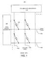
- Matrix displaysare well known in the art, where pixels are illuminated using matrix addressing as illustrated in FIG. 1.
- a typical display 100comprises a plurality of picture or display elements (pixels) 160 that are arranged in rows and columns.
- the displayincorporates a column data generator 110 and a row select generator 120 .
- each rowis sequentially activated via row line 130 , where the corresponding pixels are activated using the corresponding column lines 140 .
- each row of pixelsis illuminated sequentially one by one, whereas in an active matrix display, each row of pixels is first loaded with data sequentially. Namely, each row in the passive matrix display is only “active” for a fraction of the total frame time, whereas each row in the active matrix display can be set to be “active” for the entire total frame time.
- LCDliquid crystal display
- LEDlight-emitting diode
- a backlightis on for the entire duration in which the display is in use. Namely, all pixels in a LCD are illuminated, where a “dark” pixel is achieved by causing a polarized layer to block the illumination through that pixel. In contrast, a LED display only illuminates those pixels that are activated, thereby conserving power by not having to illuminate dark pixels.
- FIG. 2illustrates a prior art active matrix LED pixel structure 200 having two NMOS transistors N 1 and N 2 .
- the data(a voltage) is initially stored in the capacitor C by activating transistor N 1 and then activating “drive transistor” N 2 to illuminate the LED.
- a display that employs the pixel structure 200can reduce power consumption, such pixel structure exhibits nonuniformity in intensity level arising from several sources.
- the brightness of the LEDis proportional to the current passing through the LED.
- the threshold voltage of the “drive transistor” N 2may drift, thereby causing a change in the current passing through the LED. This varying current contributes to the no uniformity in the intensity of the display.
- the “drive transistor” N 2is manufactured from a material that is difficult to ensure initial threshold voltage uniformity of the transistors such that variations exist from pixel to pixel.
- LED electrical parametersmay also exhibit nonuniformity. For example, it is expected that OLED (organic light-emitting diode) turn-on voltages may increase under bias-temperature stress conditions.
- OLEDorganic light-emitting diode
- the present inventionincorporates a LED (or an OLED) pixel structure and method that improve brightness uniformity by reducing current nonuniformities in a light-emitting diode of the pixel structure.
- a pixel structure having five transistorsis disclosed.
- a pixel structure having three transistors and a diodeis disclosed.
- a different pixel structure having five transistorsis disclosed.
- an additional lineis provided to extend the autozeroing voltage range.
- an external measuring module and various external measuring methodsare disclosed to measure pixel parameters that are then used to adjust input pixel data.
- FIG. 1depicts a block diagram of a matrix addressing interface
- FIG. 2depicts a schematic diagram of a prior art active matrix LED pixel structure
- FIG. 3depicts a schematic diagram of an active matrix LED pixel structure of the present invention
- FIG. 4depicts a timing diagram for active matrix LED pixel structure of FIG. 3;
- FIG. 5depicts a schematic diagram of an alternate embodiment of an active matrix LED pixel structure of the present invention.
- FIG. 6depicts a timing diagram for active matrix LED pixel structure of FIG. 5;
- FIG. 7depicts a schematic diagram of an alternate embodiment of an active matrix LED pixel structure of the present invention.
- FIG. 8depicts a timing diagram for active matrix LED pixel structure of FIG. 7;
- FIG. 9depicts a schematic diagram of an alternate embodiment of an active matrix LED pixel structure of the present invention.
- FIG. 10depicts a schematic diagram of an alternate embodiment of an active matrix LED pixel structure of the present invention.
- FIG. 11depicts a timing diagram for active matrix LED pixel structure of FIG. 10
- FIG. 12illustrates a schematic diagram of an array of pixels interconnected into a pixel block
- FIG. 13is a schematic diagram illustrating the interconnection between a display and a display controller
- FIG. 14illustrates a flowchart of a method for initializing the display by measuring the parameters of all the pixels
- FIG. 15illustrates a flowchart of a method for correcting input data representing pixel voltages
- FIG. 16illustrates a flowchart of a method for correcting input video data representing pixel currents, i.e., luminances
- FIG. 17illustrates a flowchart of a method for initializing the display by measuring the parameters of all the pixels where the video data represent pixel voltage
- FIG. 18illustrates a flowchart of a method for correcting input video data representing pixel voltages
- FIG. 19illustrates a flowchart of a method for initializing the display by measuring the parameters of all the pixels for the situation where the video data represents pixel currents;
- FIG. 20illustrates a flowchart of a method for correcting input video data represented in pixel currents, i.e., luminances
- FIG. 21illustrates a flowchart of a method for initializing the display by measuring the parameters of all the pixels for the situation where the video data represents gamma-corrected luminance data
- FIG. 22illustrates a flowchart of a method for correcting input video data represented in gamma-corrected luminance data
- FIG. 23depicts a block diagram of a system employing a display having a plurality of active matrix LED pixel structures of the present invention.
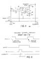
- FIG. 3depicts a schematic diagram of an active matrix LED pixel structure 300 of the present invention.
- the active matrix LED pixel structureis implemented using thin film transistors (TFTs), e.g., transistors manufactured using poly-silicon or amorphous silicon.
- TFTsthin film transistors
- the active matrix LED pixel structureincorporates an organic light-emitting diode (OLED).
- OLEDorganic light-emitting diode
- the present pixel structureis implemented using thin film transistors and an organic light-emitting diode, it should be understood that the present invention can be implemented using other types of transistors and light emitting diodes.
- the present pixel structure 300provides a uniform current drive in the presence of a large transistor threshold voltage (V t ) nonuniformity and OLED turn-on voltage nonuniformity. In other words, it is desirable to maintain a uniform current through the OLEDs, thereby ensuring uniformity in the intensity of the display.
- V ttransistor threshold voltage
- pixel structure 300comprises five NMOS transistors N 1 ( 310 ), N 2 ( 320 ), N 3 ( 330 ), N 4 ( 340 ) and N 5 ( 350 ), a capacitor 302 and a LED (OLED) (light element) 304 (light element).
- a Select line 370is coupled to the gate of transistor 350 .
- a Data line 360is coupled to one terminal of the capacitor 302 .
- An Autozero line 380is coupled to the gate of transistor 340 .
- a VDD line 390is coupled to the drain of transistors 320 and 330 .
- An Autozero line 382 from a previous row in the pixel arrayis coupled to the gate of transistor 330 .
- Autozero line 382 from a previous rowcan be implemented as a second Select line. Namely, the timing of the present pixel is such that the Autozero line 382 from a previous row can be exploited without the need of a second Select line, thereby reducing complexity and cost of the present pixel.
- One terminal of the capacitor 302is coupled (at node A) to the source of transistor 330 and to the drain of transistors 340 and 350 .
- the source of transistor 350is coupled (at node B) to the gate of transistors 310 and 320 .
- the drain of transistor 310is coupled to the source of transistor 340 .
- the source of transistors 310 and 320are coupled to one terminal of the LED 304 .
- each LED pixelis driven in a manner that is insensitive to variations in the LED turn-on voltage, as well as to variations in the TFT threshold voltages.
- the present pixelis able to determine an offset voltage parameter using an autozeroing method that is used to account for these variations in the LED turn-on voltage, and the TFT threshold voltages.
- datais provided to each pixel as a data voltage in a manner that is very similar to that used in conventional active-matrix liquid crystal displays.
- the present display architecturecan be employed with conventional column and row scanners, either external or integrated on the display plate.
- the present pixeluses five (5) TFTs and one capacitor, and the LED.
- TFTsare connected to the anode of the LED, and not the cathode, which is required by the fact that ITO is the hole emitter in conventional organic LED.
- the LEDis coupled to the source of a TFT, and not the drain.
- Each display columnhas 2 row lines (the autozero line and the select line), and 1 1 ⁇ 2 column lines (the data line and the +Vdd line, which is shared by neighboring columns).
- the waveforms on each lineare also shown in FIG. 4 .
- the operation of the pixel 300is described below in three phases or stages.
- the first phaseis a precharge phase.
- a positive pulse on the autozero (AZ) line of the previous row 382turns “on” transistor 330 and precharges node A of the pixel up to Vdd, e.g., +10 volts.
- Vdde.g. +10 volts.
- the Data linechanges from its baseline value to write data into the pixel of the previous row, and returns to its baseline. This has no net effect on the pixel under consideration.
- the second phaseis an auto-zero phase.
- the Ariz. and SELECT lines for the present rowgo high, turning “on” transistors 340 and 350 and causing the gate of transistor N 1 310 to drop, self-biasing to a turn-on voltage that permits a very small trickle of current to flow through the LED.
- the sum of the turn-on voltage of the LED and the threshold voltage of N 1are stored on the gate of N 1 . Since N 1 and N 2 can be placed very close together, their initial threshold voltages will be very similar. In addition, these two transistors should have the same gate to source voltage, Vgs.
- the threshold voltage of N 2is also stored on its gate. After auto-zeroing is complete, the Autozero line returns low, while Select line stays high.
- the third phaseis a data writing phase.
- the datais applied as a voltage above the baseline voltage on the Data line, and is written into the pixel through the capacitor. Then, the Select line returns low, and the sum of the data voltage, plus the LED turn-on voltage, plus N 2 's threshold voltage, is stored at node B for the rest of the frame. It should be noted that a capacitor from node B to +Vdd can be employed in order to protect the stored voltage from leaking away.
- the LED's turn-on voltage, as well as N 2 's threshold voltage,are “measured” and stored at node B using a trickle current.
- This auto-zero phaseis essentially a current-drive mode of operation, where the drive current is very small. It is only after the auto-zero phase, in the writing phase, that the voltage on the LED is incremented above turn-on using the applied data voltage.
- the present inventioncan be referred to as having a “hybrid drive,” rather than a voltage drive or current drive.
- the hybrid drive methodcombines the advantages of voltage drive and current drive, without the disadvantages of either. Variations in the turn-on voltage of the LED and the threshold voltage of the TFT are corrected, just as in current drive. At the same time, all lines on the display are driven by voltages, and can therefore be driven fast.
- the data voltage increment applied to the Data line 360does not appear directly across the LED 304 , but is split between Vgs of N 2 320 and the LED. This simply means that there is a nonlinear mapping from the data voltage to the LED voltage. This mapping, combined with the nonlinear mapping from LED voltage to LED current, yields the overall transfer function from data voltage to LED current, which is monotonic, and, as noted above, is stable over the life of the display.
- An advantage of the present pixel architecture 300is that the transistors in the pixel whose threshold shifts are uncorrected (N 3 , N 4 , and N 5 ) are turned on for only one row-time per frame, and therefore have a very low duty-cycle and are not expected to shift appreciably. Additionally, N 2 is the only transistor in the LED's current path. Additional transistors connected in series on this path may degrade display efficiency or may create problems due to uncorrected TFT threshold shifts, and, if shared by all pixels on a column, may introduce significant vertical crosstalk.
- Select and Autozero (AZ) pulsesare generated by row scanners.
- the column datais applied on top of a fixed (and arbitrary) baseline voltage in the time-slot between AZ pulses.
- the falling edge of Select signaloccurs while data is valid on the Data line.
- Various external and integrated column-scanner designseither of the direct-sample or chopped-ramp type, can produce data with this timing.
- the above pixel architecturepermits large direct-view displays to be built using organic LEDs.
- the present pixel structureis also applicable to any display technology that uses display elements requiring drive current, particularly, when the display elements or the TFTs have turn-on voltages that shift or are nonuniform.
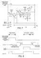
- FIG. 5depicts a schematic diagram of an alternate embodiment of an active matrix LED pixel structure 500 of the present invention.
- the pixel structure 500is similar to the pixel structure 300 of FIG. 3, where a Schottky diode is now employed in lieu in of two transistors.
- the pixel structure 300employs a single Schottky diode in each pixel that reduces the number of transistors from five to three transistors, while performing the same functions as previously described.
- pixel structure 500comprises three NMOS transistors N 1 ( 510 ), N 2 ( 520 ), N 3 ( 530 ), a capacitor 502 , a Schottky diode 540 and a LED (OLED) 550 (light element).
- a Select line 570is coupled to the gate of transistor 530 .
- a Data line 560is coupled to one terminal of the capacitor 502 .
- An Autozero line 580is coupled to the gate of transistor 520 .
- An Illuminate (similar to a VDD line) line 590is coupled to one terminal of the Schottky diode 540 .
- One terminal of the capacitor 502is coupled (at node A) to the drain of transistors 520 and 530 .
- the source of transistor 530is coupled (at node B) to the gate of transistor 510 .
- the drain of transistor 510is coupled to the source of transistor 520 , and one terminal of the Schottky diode 540 .
- the pixel structure 500also has three phases of operation: a precharge phase, an autozero phase, and a data writing phase as discussed below. All of the Illuminate lines are connected together at the periphery of the display, and before the precharge phase begins, the Illuminate lines are held at a positive voltage V ILL , which is approximately +15V. For the purpose of the following discussion, a row under consideration is referred to as “row i”. The waveforms on each line are also shown in FIG. 6 .
- the first phaseis a precharge phase. Precharge is initiated when the Autozero (AZ) line turns on transistor N 2 , and the Select line turns on transistor N 3 . This phase is performed while the Data line is at a reset level. The voltage at Nodes A and B rises to the same voltage as the drain of transistor N 1 , which is a diode drop below V ILL .
- AZAutozero
- the second phaseis an autozero phase.
- the Illuminate linedrops to ground.
- all pixels on the arraywill briefly darken.
- Autozeroing of N 1now begins with the Schottky diode 540 causing the drain of transistor N 1 to be isolated from the grounded Illuminate line.
- the AZ lineis used to turn transistor N 2 “off”, and the Illuminate line is restored to V ILL . All pixels in unselected rows light up again.
- the third phaseis a data writing phase.
- the data for row iis loaded onto the data line.
- the voltage rise at Nodes A and Bwill equal the difference between the Data line's reset voltage level and the data voltage level. Thus, variations in the threshold voltage of transistor N 1 and the LED's turn-on voltage will be compensated.
- the Select line for row iis used to turn off transistor N 3 , and the Data line is reset. The proper data voltage is now stored on the pixel until the next frame.
- a three-transistor pixel for OLED displayshas been described, that possesses the advantages described previously for the 5-transistor pixel 300 , but requires fewer transistors.
- An additional advantageis that the 5-transistor pixel employs separate transistors for autozeroing and driving the LED. Proper operation of pixel 300 requires that these two transistors have matching initial thresholds that would drift over life in the same way. Recent experimental data suggest that TFTs with different drain voltages (as these two transistors have) may not drift in the same way. Thus, pixel 500 performs autozeroing on the same transistor that drives the LED, such that proper autozeroing is guaranteed.
- FIG. 7depicts a schematic diagram of an alternate embodiment of an active matrix LED pixel structure 700 of the present invention.
- the pixel structure 700is similar to the pixel structure 300 of FIG. 3, with the exception that pixel structure 700 may generate a more precise autozero voltage.
- the autozeroingarises from the fact that each precharge cycle, as shown in FIG. 3, injects a large positive charge Q PC onto Node A of the pixel 300 .
- the precharge phasenearly all of the capacitance on Node A is from capacitor C data , such that the charge injected onto Node A is:
- V Ais the voltage that was on Node A before the precharge phase began.
- V Adepends on the threshold voltage of N 3 330 and the turn-on voltage of the LED 304 , as well as the previous data applied to the pixel 300 . Since C data is a large capacitance (approx. 1 pF), Q PC is also relatively large, on the order of ten picocoulombs.
- N 1When the pixel 300 is at a stable autozero level, Q PC flows through N 1 310 and the LED 304 during the autozero phase. Since the autozero interval is short (approximately 10 ⁇ sec.), N 1 may be left with a gate-to-source autozero voltage higher than its threshold voltage, and similarly the LED autozeroes above its turn-on voltage. Thus, the autozeroing process may not produce a true zero-current autozero voltage at Nodes A and B, but instead, an approximation of a zero-current autozero voltage.
- the pixel structure 700is capable of reducing the precharge Q PC to a very small value.
- a “variable precharge” methodis disclosed, that permits Q PC to vary, depending on the amount of charge that is actually needed for autozeroing. In brief, if the current autozero voltage is too low, Q PC assumes its maximum value of about 0.1 picocoulomb in order to raise the autozero voltage toward its desired value. However, if the current autozero voltage is too high, then Q PC is essentially zero, allowing the autozero voltage to drop quickly.
- pixel structure 700comprises five NMOS transistors N 1 ( 710 ), N 2 ( 720 ), N 3 ( 730 ), N 4 ( 740 ), N 5 ( 750 ), a capacitor 702 , and a LED (OLED) 704 (light element).
- a Select line 770is coupled to the gate of transistor 710 .
- a Data line 760is coupled to one terminal of the capacitor 702 .
- An Autozero line 780is coupled to the gate of transistor 740 .
- a VDD line 790is coupled to the drain of transistors 720 and 750 .
- An Autozero line 782 from a previous row in the pixel arrayis coupled to the gate of transistor 750 .
- Autozero line 782 from a previous rowcan be implemented as a second Select line. Namely, the timing of the present pixel is such that the Autozero line 782 from a previous row can be exploited without the need of a second Select line, thereby reducing complexity and cost of the present pixel.
- One terminal of the capacitor 702is coupled (at node A) to the drain of transistor 710 .
- the source of transistor 710is coupled (at node B) to the gate of transistors 720 and 730 and is coupled to the source of transistor 740 .
- the drain of transistor 740is coupled (at node C) to the source of transistor 750 , and to the drain of transistor 730 .
- the source of transistors 730 and 720are coupled to one terminal of the LED 704 .
- the pixel 700is similar to the pixel 300 , except that the precharge voltage is now applied to Node C, which is the drain of transistor N 3 730 .
- the precharge voltageis now applied to Node C, which is the drain of transistor N 3 730 .
- the operation of the pixel 700is again described below in three phases or stages.
- the first phaseis a precharge phase that occurs during the previous line time, i.e., before data is applied to the previous row's pixels.
- a positive pulse on the Select lineturns “on” N 1 , thereby shorting Nodes A and B together, which returns the pixel 700 to the state it was in after the last autozero phase. Namely, the pixel is returned to a data-independent voltage that is the pixel's most recent estimate of its proper autozero voltage.
- transistor N 1is “on”
- a positive pulse on the Autozero line 782 from a previous row lineturns “on” transistor N 5 , thereby precharging Node C to V dd .
- transistors N 1 and N 5are turned “off”.
- transistor N 1 and N 5are not very important, except that transistor nil must be “on” before transistor N 5 is turned “off”. Otherwise, transistor N 3 may still be turned “on” in response to the old data voltage, and the charge injected onto Node C may inadvertently drain away through transistor N 3 .
- the charge Q PCis stored at Node C on the gate-to-source/drain capacitances of transistors N 3 , N 4 and N 5 . Since these capacitances add up to a very small capacitance (about 10 fF), and the precharge interval raises Node C about 10V, Q PC is initially approximately 0.1 picocoulombs. However, this charge will drain from Node C to varying degrees prior to the autozero phase, depending on how well the previous autozero voltage approximates the true autozero voltage.
- transistors N 1 and N 5are not critical, the preferred timing is shown in FIG. 8 .
- the two transistors N 1 and N 5turn “on” at the same time in order to minimize the time required for precharge.
- N 1turns “off” before N 5 such that the (intentional) draining of Q PC from Node C is in response to a Node B voltage that has been capacitively pushed down by N 1 turning “off”. This ensures that the draining of Q PC from Node C is in response to a Node B voltage that is the same as when zero data is applied to the pixel.
- the pixel 700when compared to the pixel 300 , provides a means of precharging the pixel that allows a more effective autozeroing. Specifically, the autozeroing of pixel 700 is more accurate, faster, and data independent. Computer simulations have verified that the pixel 700 autozeroes well and is able to maintain a nearly constant OLED current vs. data voltage characteristic over an operational lifetime of 10,000 hours.
- FIG. 9depicts a schematic diagram of an alternate embodiment of an active matrix LED pixel structure 900 of the present invention.
- the pixel structure 900is similar to the pixel structure 700 of FIG. 7, with the exception of having an additional V precharge line 992 , that permits the range of autozero voltages to be extended without raising the LED supply voltage V dd . This additional modification of the pixel extends the life and efficiency of the pixel.
- the above described pixels( 200 , 300 , 700 ) have the limitation that the autozero voltage cannot exceed V dd , since this is the precharge voltage.
- V ddthe threshold voltages of transistors N 2 and N 3 drift over the life of the transistor, a point is reached where an autozero voltage higher than V dd is required in order to compensate for drift in the TFT threshold voltage and in the OLED turn-on voltage. Since the autozero voltage cannot reach higher voltages, display uniformity will quickly degrade, signaling the end of the useful life of the display. Raising V dd will permit higher autozero voltages to be achieved, but at the expense of power efficiency, since V dd is also the OLED drive supply.
- the range of autozero voltageswill be restricted even further if, in order to improve power efficiency, V dd is reduced to operate transistor N 2 in the linear region. (Of course, this will require N 2 to be made larger than if it was operated in saturation.) In this case, the operating lifetime will be quite short, since after a short period of operation, the autozero voltage will need to reach a level higher than V dd .
- an optional modificationis incorporated into the pixel 700 that removes restrictions on the autozero voltage, thereby permitting it to be extended to well above V dd .
- the pixel 900is identical to the pixel 700 with the exception of an additional column line 992 , that is coupled to the drain of transistor 950 .
- the column line 992is added to the array to carry a DC voltage V precharge to all the pixels. All of these column lines are connected together at the edge of the display. By raising V precharge to a level higher than V dd , the pixel 900 can precharge and autozero to a voltage higher than V dd . A high value of V precharge will have very little effect on display efficiency.
- each V preharge line 992can be shared by neighboring columns of pixels.
- the V precharge linescan also run as row lines, shared by neighboring rows.
- pixel structuresare designed for an OLED display in such a manner that transistor threshold voltage variations and OLED turn-on voltage variations in the pixel can be compensated, these pixel structures are not designed to address nonuniformity that is generated external to the pixel. It was pointed out that the pixel could be used with conventional column driver circuits, either external to the display plate or integrated on the display.
- integrated data driversare typically not as accurate as external drivers. While commercially available external drivers can achieve ⁇ 12 mV accuracy, it has proven difficult to achieve accuracy better than ⁇ 50 mV using integrated drivers.
- the particular type of error produced by integrated driversis primarily offset error, i.e., it is a data-independent DC level that adds to all data voltages.
- the offset erroris nonuniform, i.e., the value of the DC level varies from one data driver to the next.
- Liquid crystal displaystend to be forgiving of offset errors because the liquid crystal is driven with opposite polarity data in successive frames, such that in one frame the offset error causes the liquid crystal to be slightly too dark, and in the next frame too light, but the average is nearly correct and the alternating errors are not noticeable to the eye.
- an OLED pixelis driven with unipolar data. Therefore, the bipolar cancellation of offset errors does not occur, and serious nonuniformity problems may result when integrated scanners are used.
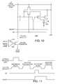
- FIG. 10depicts a schematic diagram of an active matrix LED pixel structure 300 of the present invention coupled to a data driver 1010 via a column transistor 1020 .
- the present inventiondescribes a method for canceling offset errors in integrated data scanners for OLED displays. Namely, the present method is designed to operate with any pixel in which the pixel is capacitively coupled to a data line, and has an autozero phase, e.g., pixels 200 , 300 , 500 , and 700 as discussed above.
- the pixel 300 as described aboveis coupled to a Data line that provides the pixel with an analog level to establish the brightness of the OLED element.
- the Data lineis driven by a data driver that uses the chopped ramp technique to set the voltage on the Data line.
- Various sources of error exist in this approachthat may give rise to offset errors on the Data line.
- the time at which the voltage comparator s itchescan vary depending on the comparator's maximum slew rate. It has also been observed experimentally that the maximum slew rate can be highly variable.
- the offset errorwill affect the voltage stored in the pixel. Since it is nonuniform, the offset error will also lead to brightness variations across the display.
- the period during which the pixel autozeros to cancel its own internal threshold erroris also used to calibrate out the data scanner's offset error.
- the waveforms of the various linesis shown in FIG. 11 .
- This reference black level, applied during the pixel's autozero phase,is set on the Data line in exactly the same manner that the actual data voltage will be set: the data ramp is chopped at a time determined by the voltage comparator.
- the voltage across capacitor C of the pixelis determined by the difference between the pixel's turn-on voltage and the combined black level plus the offset error voltage.
- the reference black levelis maintained for the entire autozero phase.
- This techniquecan be applied not only to integrated scanners that use a chopped ramp, but also to scanners using direct sampling onto the columns.
- direct samplingthe error arises from the nonuniform capacitive feedthrough of the gate signal onto the Data line when the (large) column transistor turns off. Variations in the threshold voltage of this transistor produce a nonuniform offset error, just like the nonuniform offset error produced by the chopped ramp data scanners.
- a black reference voltageis written onto the columns during the pixel's autozero phase. Since all of the pixels in a row autozero at the same time, this black level is written onto all of the data columns simultaneously at the beginning of the line time. The black level is maintained for the entire autozero phase.
- the offset errorwill be canceled by the voltage stored on the pixel capacitor.
- the time overhead required to perform offset error correctionis smaller using the direct-sampling technique than with the chopped ramp technique.
- the present method for correcting data driver errorsshould permit organic LED displays to be built with much better brightness uniformity than would otherwise be possible. Using the method described here, together with any of the above autozeroing pixels, brightness uniformity of 8-bits should be achievable, with no visible uniformity degradation over the lifetime of the display.
- the above disclosuredescribes a plurality of pixel structures that can be employed to account for nonuniformity in the intensity of a display
- an alternative approachis to compensate such nonuniformity by using external means. More specifically, the disclosure below describes an external calibration circuit and method to account for nonuniformity in the intensity of a display.
- the non-uniformityis measured and stored for all the pixels such that the data (e.g., data voltages) can be calibrated using the measured non-uniformity.
- the present external calibration circuit and methodcan be employed with other pixel structures, including but not limited to, the pixels 300 , 500 , and 700 as described above.
- a more simplified pixel structurecan be employed in the display, thereby increasing display yield and fill-factor.
- FIG. 12illustrates a schematic diagram of an array of pixels 200 interconnected into a pixel block 1200 .
- datais written into the pixel array in the manner commonly used with active matrix displays. Namely, a row of pixels is selected by driving the Select line high, thereby turning on access transistor N 1 . Data is written into the pixels in this row by applying data voltages to the Data lines. After the voltage at node A has settled, the row is deselected by driving the Select line low. The data voltage is stored at node A until this row is selected again on the next frame. There may be some charge leakage from node A during the time that N 1 is turned off, and a storage capacitor may be required at node A to prevent an unacceptable level of voltage decay.
- the dotted linesillustrate how a capacitor can be connected to address the voltage decay. However, it is possible that there is sufficient capacitance associated with the gate of N 2 to render such additional capacitance unnecessary.
- the luminance L of an OLEDis approximately proportional to its current I, with the constant of proportionality being fairly stable and uniform across the display. Therefore, the display will be visually uniform if well-defined OLED currents are produced.
- the present inventiondescribes a method for correcting the data voltage applied to the gate of N 2 in such a way that variations in the TFT and OLED electrical parameters are compensated, thereby permitting well-defined OLED currents to be produced in the pixel array.
- FIGS. 2 and 12illustrate a pixel array having VDD supply lines that are disposed parallel to the Data lines. (In alternative embodiments, the VDD lines may run parallel to the Select lines.) As such, each VDD line can be shared by two or more neighboring columns of pixels to reduce the number of VDD lines.
- FIG. 12illustrates the VDD lines as being tied together into blocks on the periphery of the display. Each pixel block 1200 may contain as few as one VDD line, or as many as the total number of VDD lines on the display. However, in the preferred embodiment, each pixel block 1200 contain about 24 VDD lines, i.e., about 48 pixel columns.
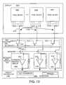
- FIG. 13is a schematic diagram illustrating the interconnection between a display 1310 and a display controller 1320 .
- the display 1310comprises a plurality of pixel blocks 1200 .
- the display controller 1320comprises a VDD control module 1350 , a measurement module 1330 and various I/O devices 1340 such as A/D converters and a memory for storing pixel parameters.
- Each pixel blockis coupled to a sensing pin (VDD/SENSE) 1210 at the edge of the display, as shown in FIGS. 12 and 13.
- the sensing pins 1210are switched to an external V dd supply, e.g., between 10-15V, thereby supplying current to the display for illuminating the OLED elements.
- each VDD/SENSE pin 1210is associated with a pair of p-channel transistors P 1 ( 1352 ) and P 2 ( 1332 ) and a current sensing circuit 1334 in the display controller 1320 .
- an ILLUMINATE signal from the display controlleractivates P 1 to connect a VDD/SENSE pin to the V dd supply.
- the current through P 1is expected to be approximately 1 mA per column.
- the external current sensing circuits 1334are activated via a MEASURE signal to collect information about each pixel's parameters during a special measurement cycle. The collected information is used to calculate or adjust the appropriate data voltages for establishing the desired OLED currents during normal display operation.
- all other pixels in the pixel blockare tuned off by loading these pixels with low data voltages (e.g., zero volts or less), thereby ensuring negligible current draw from the “off” pixels.
- the current drawn by the pixel of interestis measured in response to one or more applied data voltages.
- the data patterni.e., consisting of all pixels in a block turned “off” except for one pixel turned “on”
- the displayis partitioned into a plurality of pixel blocks, a plurality of pixels can be measured by turning on at least one pixel in each pixel block simultaneously.
- the current drawn by the pixel of interest in each pixel blockis measured externally by driving the ILLUMINATE and MEASURE lines to levels that disconnect the VDD/SENSE pin 1210 from VDD source and connect the sensing pin to the input of a current-sensing circuit 1334 through P 2 , where the current drawn by the pixel of interest is measured.
- the pixel currentis expected to be in the range of 1-10 uA.
- the current-sensing circuit 1334is shown as a transimpedance amplifier in FIG. 13, but other embodiments of current-sensing circuit can be implemented. In the present invention, the amplifier generates a voltage at the output that is proportional to the current at the input. This measured information is then collected by I/O devices 1340 where the information is converted into digital form and then stored for calibrating data voltages.
- the resistor in the current-sensing circuit 1334is approximately one Megohm.
- multiple current-sensing circuits 1334are illustrated with a one to one correspondence with the pixel blocks, fewer current-sensing circuits can be employed through the use of a multiplexer (not shown). Namely, multiple VDD/SENSE pins are multiplexed to a single current-sensing circuit 1334 . In one extreme, a single current-sensing circuit is used for the entire display. Multiplexing the VDD/SENSE pins to the sensing circuits in this manner reduces the complexity of the external circuitry, but at the expense of added display measurement time.
- pixel measurementsshould be scheduled in a manner that will least disrupt the viewer. Since the pixel parameters change slowly, a given pixel does not need to be measured frequently, and measurement cycles can be spread over a long period of time.
- compensation or calibration of the data voltagescan be applied to the display to correct for various sources of display nonuniformity.
- compensation of the data voltagescan be performed to account for transistor threshold-voltage variations and OLED turn-on voltage variations.
- the discussion belowdescribes a plurality of methods that are capable of compensating the above sources of display nonuniformity, including other sources of display nonuniformity as well. By using these methods, a display with several sources of nonuniformity, some of them severe, can still provide a uniform, high-quality displayed image.
- the stored voltage on Node Ais the gate voltage of N 2 , and thus establishes a current through N 2 and through the LED.
- the gate voltage on N 2the LED current can be varied.
- the gate voltage V gcan be divided into two parts, the gate-to-source voltage V gs of N 2 and the voltage V diode across the LED:
- V gV gs +V diode (2)
- Ik 2 ⁇ ( V gs - V t ) 2 ( 3 )
- V gs2 ⁇ I k + V t ( 4 )
- the forward current through the OLEDis approximately:
- V diodeI A m ( 6 )
- V gV t + 2 ⁇ I k + I A m ( 7 )
- the present inventionis not limited to the detailed functional form of the OLED I-V characteristic as disclosed above, and as such, can be adapted to operate for any diode-like characteristic.
- the luminance L of an OLEDis approximately proportional to its current I, with the constant of proportionality being fairly stable and uniform across the display.
- the displayis visually uniform if well-defined OLED currents can be produced.
- the pixelis programmed with the voltage V g and not the current I.
- TFT parameters V t and kwill exhibit some initial nonuniformity across a display, as well OLED parameters A and m. Furthermore, it is well known that V t increases under bias-temperature stress conditions.
- the OLED parameter Ais directly related to the OLED's turn-on voltage, and is known to decrease under bias stress.
- the OLED parameter mis related to the distribution of traps in the organic band gap, and may also vary over the life of the OLED.
- these parametersare expected to be initially nonuniform, and to vary over the life of the display in a manner that depends on the individual bias history of each pixel. Programming the gate voltage without compensating for the variations of these parameters will yield a display that is initially nonuniform, with increasing nonuniformity over the life of the display.
- the gate voltage V gis not necessarily equal to the intended data voltage V data .
- gain and offset errors in the data drivers, as well as (data-dependent) feedthrough arising from the deselection of N 1may cause these two voltages to be different.
- These sources of errorcan also be nonuniform and can vary over the life of the display.
- V gBV data +V 0 (8)
- V dataV off + C ⁇ I + D ⁇ I m ( 9 )
- V off , C, and Dare combinations of the earlier parameters.
- the present inventionprovides various compensation methods for correcting the intended (input) data voltage V data to compensate for variations in V off , C, D, and m, thereby permitting well-defined OLED currents to be produced in the pixel array.
- the external current sensing circuitsas described above, collect information about each pixel's parameters, i.e., the current drawn by a single pixel can be measured externally.
- the present inventionuses the measured information for the parameters V off , C, D, and m, calculates the appropriate data voltages V data in accordance with equation (9), for establishing the desired OLED currents during normal display operation.
- pixel nonuniformityis characterized using only two parameters instead of four as discussed above. Referring to the pixel's current-voltage characteristic of equation (9), at normal illumination levels, the C ⁇ square root over (I) ⁇ term, associated with V gs of N 2 , and the D ⁇ I m
- V diodeV diode
- equation (9)can be approximated as:
- V dataV offset +C ⁇ square root over (I) ⁇ (10)
- V offsetV off + D ⁇ I m
- V offset and Cvary from pixel to pixel.
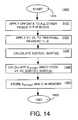
- FIG. 14illustrates a flowchart of a method 1400 for initializing the display by measuring the parameters of all the pixels.
- Method 1400starts in step 1405 and proceeds to step 1410 , where an “off” data voltage is applied to all pixels in a pixel block, except for the pixel of interest.
- step 1420to determine V offset and C for a given pixel of interest, method 1400 applies two data voltages (V 1 and V 2 ), and the current is measured for each data voltage.
- step 1430the square root of the currents I 1 and I 2 are calculated.
- a square root tableis used in this calculation.
- V offset and Care determined, i.e., two equations are available to solve two variables.
- the calculated V offset and C for a given pixel of interestare stored in a storage, e.g., memory.
- the memorycontains the two parameters V offset and C for each pixel in the array. These values can be used at a later time to calibrate or adjust V data in accordance with equation (10).
- Method 1400then ends in step 1455 .
- this conditioncan be satisfied by making one measurement at the highest data voltage that the system can generate, and then the other measurement at a slightly lower data voltage.
- the raw input video data supplied to the display modulecan be corrected.
- the input video datacan exist in various formats, e.g., the video data can represent (1) pixel voltages, (2) gamma-corrected pixel luminances, or (3) pixel currents.
- the use of the stored parameters V offset and C to calibrate or adjust the input video datadepends on each specific format.
- FIG. 15illustrates a flowchart of a method 1500 for correcting input video data representing pixel voltages.
- Method 1500starts in step 1505 and proceeds to step 1510 , where the stored parameters, e.g., V offset and C are retrieved for a pixel of interest.
- the stored parameterse.g., V offset and C are retrieved for a pixel of interest.
- the division by C 0can be avoided if the video data V data has already been scaled by the constant factor 1/C 0 .
- the multiplication by Ccan be performed directly in digital logic, or using at look-up table. For example, in the latter case, each value of C specifies a table where the value of the video data is an index, and the table entries consist of the result of the multiplication. (Alternatively, the roles of C and the input video data in the look-up table can be reversed.) After the multiplication is performed, rapid addition of V offset can be implemented with digital logic.
- step 1530the resulting voltage V data , i.e., the corrected or adjusted input data, is then forwarded to the data driver of pixel array.
- Method 1500then ends in step 1535 .
- the input video dataare proportional to L 0.45 , where L is luminance. This is typical for video data that have been pre-corrected for CRT luminance-voltage characteristics. Since L 0.45 ⁇ square root over (L) ⁇ , and the OLED luminance is proportional to its current, the data can be treated as proportional to ⁇ square root over (I) ⁇ . Thus, the calculation can be performed in the same way as for zero-offset voltage data as discussed above.
- FIG. 16illustrates a flowchart of a method 1600 for correcting input video data representing pixel currents, i.e., luminances.
- Method 1600starts in step 1605 and proceeds to step 1610 , where the square-root values of the measured current are calculated.
- method 1600is similar to the method 1500 described above, with the exception that the video data representing I must be processed to yield ⁇ square root over (I) ⁇ .
- this operationcan be implemented using a table that provides square-root values as needed for deriving the pixel parameters V offset and C from pixel current measurements, as illustrated in FIG. 14 .
- this tableis used again to generate ⁇ square root over (I) ⁇ from the video data.
- the data correction steps 1610 - 1645 of method 1600are identical to the method 1500 as described above, with the exception that the square root of the input data is multiplied by C in step 1630 and then followed by an addition of V offset to yield the corrected data voltage.
- pixel nonuniformityis characterized using only one parameter instead of two or four parameters as discussed above. Namely, an additional simplification is made such that pixel nonuniformity is characterized using a single parameter.
- V offsetthe only significant source of nonuniformity. This occurs when the TFT transconductance parameter k and the voltage gain factor B are uniform. In this case, it is sufficient to determine each pixel's V offset Then, data correction does not involve multiplication (since the gain factor C is assumed to be uniform), but only involves addition of the offset parameter.
- This one-parameter approximationis similar to the above autozeroing OLED pixel structures.
- the present one-parameter compensation methodshould produce satisfactory display uniformity, while reducing computational expense.
- the above described two or four-parameter methodscan be employed at the expense of increasing computational complexity and expense.
- the display initialization processdepends on the format of the data.
- the single-parameter methodcan be used to initialize the display and to correct video data for the cases of video data representing (1) pixel voltages, (2) pixel currents, and (3) gamma-corrected pixel luminances.
- FIG. 17illustrates a flowchart of a method 1700 for initializing the display by measuring the parameters of all the pixels.
- Method 1700starts in step 1705 and proceeds to step 1710 , where an “off” data voltage is applied to all pixels in a pixel block, except for the pixel of interest.
- step 1720to determine V offset and C for a given pixel of interest, method 1700 applies two data voltages (V 1 and V 2 ), and the current is measured for each data voltage.
- step 1730the square root of the currents I 1 and I 2 are calculated.
- a square root tableis used in this calculation.
- step 1740the average C is determined. Namely, using a table to calculate ⁇ square root over (I) ⁇ for each current measurement, an average value of C for the display can be calculated.
- V offsetis determined for each pixel from its current measurements based on the average C. In this manner, small variations in C across the display are partially compensated by the calculated V offset . For reasons given above, it is preferable to make each pixel's current measurement at the highest possible data voltage.
- each pixel's V offsetis stored in a storage, e.g., memory.
- Method 1700then ends in step 1765 .
- FIG. 18illustrates a flowchart of a method 1800 for correcting input video data representing pixel voltages.
- Method 1800starts in step 1805 and proceeds to step 1810 , where the stored parameters, e.g., V offset is retrieved for a pixel of interest.
- step 1830the resulting voltage V data , i.e., the corrected or adjusted input data, is then forwarded to the data driver of pixel array.
- Method 1800then ends in step 1835 .
- FIG. 19illustrates a flowchart of a method 1900 for initializing the display by measuring the parameters of all the pixels for the situation where the video data represents pixel currents.
- method 1900is very similar to method 1700 as discussed above.
- the tableis expected to provide a more accurate representation of the pixel's current-voltage characteristics than the square-root function.
- the tableis then stored in a storage, e.g., a memory for later use. Then the individual pixel current measurements are used as indexes to enter this table, and individual pixel offsets V offset are determined.
- FIG. 20illustrates a flowchart of a method 2000 for correcting input video data represented in pixel currents, i.e., luminances.
- Method 2000starts in step 2005 and proceeds to step 2010 , where the current pixel of interest's V offset is retrieved from storage.
- step 2020the zero-offset data voltage vs. pixel current table is used to obtain a zero-offset data voltage from the input video data current. This zero-offset data voltage is added to the retrieved V offset in step 2030 . Finally, in step 2040 , the corrected or adjusted input video data, is then forwarded to the data driver of the pixel array.
- the zero-offset data voltage corresponding to each currentis looked up in the V-I table. Then the stored pixel offset is added to the zero-offset voltage, and the result is the input to the data driver. Method 2000 then ends in step 2045 .
- FIG. 21illustrates a flowchart of a method 2100 for initializing the display by measuring the parameters of all the pixels for the situation where the video data represents gamma-corrected luminance data.
- method 2100is very similar to method 1900 as discussed above.
- a calculated average value of Cis used to generate a table of zero-offset data voltage vs. the square root of the pixel current.
- the video datacan be approximated as representing ⁇ square root over (I) ⁇ .
- the average value of Cis used to create a zero-offset table of V data vs. ⁇ square root over (I) ⁇ , and this table is saved in a storage such as a memory.
- FIG. 22illustrates a flowchart of a method 2200 for correcting input video data represented in gamma-corrected luminance data. It should be noted that method 2200 is very similar to method 2000 as discussed above. The only exception arises in the zero-offset table of V data vs. ⁇ square root over (I) ⁇ . Thus, in sum, incoming video data are used to look up the zero-offset data voltages, and stored pixel offsets are added to these voltages.
- V dataV off + C ⁇ ( I ) ⁇ I + D ⁇ I m ( 11 )
- V offV off , if the current is sufficiently high, such that only an offset term and a gain factor need to be determined as discussed above.
- the two-parameter correction methodwill likely perform significantly better than the one-parameter correction method, if N 2 is operated in the linear region.
- FIG. 23illustrates a block diagram of a system 2300 employing a display 2320 having a plurality of active matrix LED pixel structures 300 , 500 , or 700 of the present invention.
- the system 2300comprises a display controller 2310 and a display 2320 .
- the display controllercan be implemented as a general purpose computer having a central processing unit CPU 2312 , a memory 2314 and a plurality of I/O devices 2316 (e.g., a mouse, a keyboard, storage devices, e.g., magnetic and optical drives, a modem, A/D converter, various modules, e.g., measurement module 1330 as discussed above, and the like).
- Software instructionse.g., the various methods described above
- the software instructions of the present inventioncan be stored on a computer-readable medium.
- the display 2320comprises a pixel interface 2322 and a plurality of pixels (pixel structures 300 , 500 , or 700 ).
- the pixel interface 2322contains the necessary circuitry to drive the pixels 300 , 500 , or 700 .
- the pixel interface 2322can be a matrix addressing interface as illustrated in FIG. 1 and may optionally include additional signal/control lines as discussed above.
- the system 2300can be implemented as a laptop computer.
- the display controller 2310can be implemented in other manners such as a microcontroller or application specific integrated circuit (ASIC) or a combination of hardware and software instructions.
- the system 2300can be implemented within a larger system that incorporates a display of the present invention.
Landscapes
- Engineering & Computer Science (AREA)
- Physics & Mathematics (AREA)
- Computer Hardware Design (AREA)
- General Physics & Mathematics (AREA)
- Theoretical Computer Science (AREA)
- Control Of Indicators Other Than Cathode Ray Tubes (AREA)
- Control Of El Displays (AREA)
- Electroluminescent Light Sources (AREA)
- Devices For Indicating Variable Information By Combining Individual Elements (AREA)
- Led Devices (AREA)
Abstract
Description


Claims (4)
Priority Applications (1)
| Application Number | Priority Date | Filing Date | Title |
|---|---|---|---|
| US09/793,933US6618030B2 (en) | 1997-09-29 | 2001-02-27 | Active matrix light emitting diode pixel structure and concomitant method |
Applications Claiming Priority (4)
| Application Number | Priority Date | Filing Date | Title |
|---|---|---|---|
| US6038797P | 1997-09-29 | 1997-09-29 | |
| US6038697P | 1997-09-29 | 1997-09-29 | |
| US09/161,862US6229508B1 (en) | 1997-09-29 | 1998-09-28 | Active matrix light emitting diode pixel structure and concomitant method |
| US09/793,933US6618030B2 (en) | 1997-09-29 | 2001-02-27 | Active matrix light emitting diode pixel structure and concomitant method |
Related Parent Applications (1)
| Application Number | Title | Priority Date | Filing Date |
|---|---|---|---|
| US09/161,862DivisionUS6229508B1 (en) | 1997-09-29 | 1998-09-28 | Active matrix light emitting diode pixel structure and concomitant method |
Publications (2)
| Publication Number | Publication Date |
|---|---|
| US20010024186A1 US20010024186A1 (en) | 2001-09-27 |
| US6618030B2true US6618030B2 (en) | 2003-09-09 |
Family
ID=26739867
Family Applications (2)
| Application Number | Title | Priority Date | Filing Date |
|---|---|---|---|
| US09/161,862Expired - Fee RelatedUS6229508B1 (en) | 1997-09-29 | 1998-09-28 | Active matrix light emitting diode pixel structure and concomitant method |
| US09/793,933Expired - LifetimeUS6618030B2 (en) | 1997-09-29 | 2001-02-27 | Active matrix light emitting diode pixel structure and concomitant method |
Family Applications Before (1)
| Application Number | Title | Priority Date | Filing Date |
|---|---|---|---|
| US09/161,862Expired - Fee RelatedUS6229508B1 (en) | 1997-09-29 | 1998-09-28 | Active matrix light emitting diode pixel structure and concomitant method |
Country Status (4)
| Country | Link |
|---|---|
| US (2) | US6229508B1 (en) |
| EP (1) | EP0905673B1 (en) |
| JP (2) | JP3767877B2 (en) |
| DE (1) | DE69840254D1 (en) |
Cited By (148)
| Publication number | Priority date | Publication date | Assignee | Title |
|---|---|---|---|---|
| US20020126075A1 (en)* | 2001-03-12 | 2002-09-12 | Willis Donald Henry | Reducing sparkle artifacts with post gamma correction slew rate limiting |
| US20030057895A1 (en)* | 2001-09-07 | 2003-03-27 | Semiconductor Energy Laboratory Co., Ltd. | Light emitting device and method of driving the same |
| US20030142088A1 (en)* | 2001-10-19 | 2003-07-31 | Lechevalier Robert | Method and system for precharging OLED/PLED displays with a precharge latency |
| US20040007989A1 (en)* | 2002-07-12 | 2004-01-15 | Au Optronics Corp. | Driving circuit for unit pixel of organic light emitting displays |
| US20040130543A1 (en)* | 2003-01-03 | 2004-07-08 | Wein-Town Sun | Method for reducing power consumption of an LCD panel in a standby mode |
| US20050052377A1 (en)* | 2003-09-08 | 2005-03-10 | Wei-Chieh Hsueh | Pixel driving circuit and method for use in active matrix OLED with threshold voltage compensation |
| US20050068275A1 (en)* | 2003-09-29 | 2005-03-31 | Kane Michael Gillis | Driver circuit, as for an OLED display |
| US20050067971A1 (en)* | 2003-09-29 | 2005-03-31 | Michael Gillis Kane | Pixel circuit for an active matrix organic light-emitting diode display |
| US6876348B2 (en)* | 2001-01-10 | 2005-04-05 | Kabushiki Kaisha Toshiba | Display device equipped with SRAM in pixel and driving method of the same |
| US20050156831A1 (en)* | 2002-04-23 | 2005-07-21 | Semiconductor Energy Laboratory Co., Ltd. | Light emitting device and production system of the same |
| WO2006000101A1 (en)* | 2004-06-29 | 2006-01-05 | Ignis Innovation Inc. | Voltage-programming scheme for current-driven amoled displays |
| US20060007078A1 (en)* | 2004-07-06 | 2006-01-12 | Au Optronics Corp. | Active matrix organic light emitting diode (AMOLED) display panel and a driving circuit thereof |
| US20060028407A1 (en)* | 2004-08-06 | 2006-02-09 | Chen-Jean Chou | Light emitting device display circuit and drive method thereof |
| US20060038762A1 (en)* | 2004-08-21 | 2006-02-23 | Chen-Jean Chou | Light emitting device display circuit and drive method thereof |
| US20060050040A1 (en)* | 2004-09-03 | 2006-03-09 | Chen-Jean Chou | Active Matrix Light Emitting Device Display and Drive Method Thereof |
| US20060066527A1 (en)* | 2004-09-24 | 2006-03-30 | Chen-Jean Chou | Active matrix light emitting device display pixel circuit and drive method |
| US20060071887A1 (en)* | 2004-10-01 | 2006-04-06 | Chen-Jean Chou | Active matrix display and drive method thereof |
| US20060114192A1 (en)* | 2001-08-02 | 2006-06-01 | Seiko Epson Corporation | Driving of data lines used in unit circuit control |
| WO2006130981A1 (en)* | 2005-06-08 | 2006-12-14 | Ignis Innovation Inc. | Method and system for driving a light emitting device display |
| US20070008253A1 (en)* | 2005-07-06 | 2007-01-11 | Arokia Nathan | Method and system for driving a pixel circuit in an active matrix display |
| US20070052634A1 (en)* | 2000-02-29 | 2007-03-08 | Semiconductor Energy Laboratory Co., Ltd. | Light-Emitting Device |
| US20070063932A1 (en)* | 2005-09-13 | 2007-03-22 | Arokia Nathan | Compensation technique for luminance degradation in electro-luminance devices |
| US20070152919A1 (en)* | 2006-01-04 | 2007-07-05 | Toppoly Optoelectronics Corp. | Pixel unit and display and electronic device utilizing the same |
| US20070164959A1 (en)* | 2004-01-07 | 2007-07-19 | Koninklijke Philips Electronic, N.V. | Threshold voltage compensation method for electroluminescent display devices |
| US20070195020A1 (en)* | 2006-02-10 | 2007-08-23 | Ignis Innovation, Inc. | Method and System for Light Emitting Device Displays |
| US20070236440A1 (en)* | 2006-04-06 | 2007-10-11 | Emagin Corporation | OLED active matrix cell designed for optimal uniformity |
| US20070247398A1 (en)* | 2006-04-19 | 2007-10-25 | Ignis Innovation Inc. | Stable driving scheme for active matrix displays |
| US20080055223A1 (en)* | 2006-06-16 | 2008-03-06 | Roger Stewart | Pixel circuits and methods for driving pixels |
| US20080062091A1 (en)* | 2006-06-16 | 2008-03-13 | Roger Stewart | Pixel circuits and methods for driving pixels |
| US20080062090A1 (en)* | 2006-06-16 | 2008-03-13 | Roger Stewart | Pixel circuits and methods for driving pixels |
| US20080136338A1 (en)* | 2006-12-11 | 2008-06-12 | Lehigh University | Active matrix display and method |
| WO2007149233A3 (en)* | 2006-06-16 | 2008-09-25 | Kotab Dominic M | Pixel circuits and methods for driving pixels |
| US20090015575A1 (en)* | 2005-12-20 | 2009-01-15 | Philippe Le Roy | Method for Controlling a Display Panel by Capacitive Coupling |
| US20090262101A1 (en)* | 2008-04-16 | 2009-10-22 | Ignis Innovation Inc. | Pixel circuit, display system and driving method thereof |
| US20100020056A1 (en)* | 2005-12-20 | 2010-01-28 | Philippe Le Roy | Display Panel and Control Method Using Transient Capacitive Coupling |
| US20100033469A1 (en)* | 2004-12-15 | 2010-02-11 | Ignis Innovation Inc. | Method and system for programming, calibrating and driving a light emitting device display |
| US20100039458A1 (en)* | 2008-04-18 | 2010-02-18 | Ignis Innovation Inc. | System and driving method for light emitting device display |
| US20110128262A1 (en)* | 2009-12-01 | 2011-06-02 | Ignis Innovation Inc. | High resolution pixel architecture |
| US20110134094A1 (en)* | 2004-11-16 | 2011-06-09 | Ignis Innovation Inc. | System and driving method for active matrix light emitting device display |
| US7978187B2 (en) | 2003-09-23 | 2011-07-12 | Ignis Innovation Inc. | Circuit and method for driving an array of light emitting pixels |
| US20110191042A1 (en)* | 2010-02-04 | 2011-08-04 | Ignis Innovation Inc. | System and methods for extracting correlation curves for an organic light emitting device |
| US8026876B2 (en) | 2006-08-15 | 2011-09-27 | Ignis Innovation Inc. | OLED luminance degradation compensation |
| US20120086694A1 (en)* | 2010-10-08 | 2012-04-12 | Au Optronics Corp. | Pixel circuit and display panel with ir-drop compensation function |
| CN101228569B (en)* | 2005-06-08 | 2012-07-04 | 伊格尼斯创新有限公司 | Method and system for driving a light emitting device display |
| US8576217B2 (en) | 2011-05-20 | 2013-11-05 | Ignis Innovation Inc. | System and methods for extraction of threshold and mobility parameters in AMOLED displays |
| US8599191B2 (en) | 2011-05-20 | 2013-12-03 | Ignis Innovation Inc. | System and methods for extraction of threshold and mobility parameters in AMOLED displays |
| US8659518B2 (en) | 2005-01-28 | 2014-02-25 | Ignis Innovation Inc. | Voltage programmed pixel circuit, display system and driving method thereof |
| US8664644B2 (en) | 2001-02-16 | 2014-03-04 | Ignis Innovation Inc. | Pixel driver circuit and pixel circuit having the pixel driver circuit |
| US8803417B2 (en) | 2009-12-01 | 2014-08-12 | Ignis Innovation Inc. | High resolution pixel architecture |
| US8816943B2 (en) | 2008-10-16 | 2014-08-26 | Global Oled Technology Llc | Display device with compensation for variations in pixel transistors mobility |
| US8901579B2 (en) | 2011-08-03 | 2014-12-02 | Ignis Innovation Inc. | Organic light emitting diode and method of manufacturing |
| US8907991B2 (en) | 2010-12-02 | 2014-12-09 | Ignis Innovation Inc. | System and methods for thermal compensation in AMOLED displays |
| US8922544B2 (en) | 2012-05-23 | 2014-12-30 | Ignis Innovation Inc. | Display systems with compensation for line propagation delay |
| US8994617B2 (en) | 2010-03-17 | 2015-03-31 | Ignis Innovation Inc. | Lifetime uniformity parameter extraction methods |
| US9030506B2 (en) | 2009-11-12 | 2015-05-12 | Ignis Innovation Inc. | Stable fast programming scheme for displays |
| US9058775B2 (en) | 2006-01-09 | 2015-06-16 | Ignis Innovation Inc. | Method and system for driving an active matrix display circuit |
| US9070775B2 (en) | 2011-08-03 | 2015-06-30 | Ignis Innovations Inc. | Thin film transistor |
| US9087476B2 (en) | 2000-01-17 | 2015-07-21 | Semiconductor Energy Laboratory Co., Ltd. | Display system and electrical appliance |
| US9093028B2 (en) | 2009-12-06 | 2015-07-28 | Ignis Innovation Inc. | System and methods for power conservation for AMOLED pixel drivers |
| US9111485B2 (en) | 2009-06-16 | 2015-08-18 | Ignis Innovation Inc. | Compensation technique for color shift in displays |
| US9134825B2 (en) | 2011-05-17 | 2015-09-15 | Ignis Innovation Inc. | Systems and methods for display systems with dynamic power control |
| US9153172B2 (en) | 2004-12-07 | 2015-10-06 | Ignis Innovation Inc. | Method and system for programming and driving active matrix light emitting device pixel having a controllable supply voltage |
| US9171504B2 (en) | 2013-01-14 | 2015-10-27 | Ignis Innovation Inc. | Driving scheme for emissive displays providing compensation for driving transistor variations |
| US9171500B2 (en) | 2011-05-20 | 2015-10-27 | Ignis Innovation Inc. | System and methods for extraction of parasitic parameters in AMOLED displays |
| US9190456B2 (en) | 2012-04-25 | 2015-11-17 | Ignis Innovation Inc. | High resolution display panel with emissive organic layers emitting light of different colors |
| US9202412B2 (en) | 2010-03-25 | 2015-12-01 | Joled Inc. | Organic EL display apparatus and method of fabricating organic EL display apparatus |
| US9208721B2 (en) | 2010-03-25 | 2015-12-08 | Joled Inc. | Organic EL display apparatus and method of fabricating organic EL display apparatus |
| US9269322B2 (en) | 2006-01-09 | 2016-02-23 | Ignis Innovation Inc. | Method and system for driving an active matrix display circuit |
| US9275579B2 (en) | 2004-12-15 | 2016-03-01 | Ignis Innovation Inc. | System and methods for extraction of threshold and mobility parameters in AMOLED displays |
| US9280933B2 (en) | 2004-12-15 | 2016-03-08 | Ignis Innovation Inc. | System and methods for extraction of threshold and mobility parameters in AMOLED displays |
| US9305488B2 (en) | 2013-03-14 | 2016-04-05 | Ignis Innovation Inc. | Re-interpolation with edge detection for extracting an aging pattern for AMOLED displays |
| US9311859B2 (en) | 2009-11-30 | 2016-04-12 | Ignis Innovation Inc. | Resetting cycle for aging compensation in AMOLED displays |
| US9324268B2 (en) | 2013-03-15 | 2016-04-26 | Ignis Innovation Inc. | Amoled displays with multiple readout circuits |
| US9336717B2 (en) | 2012-12-11 | 2016-05-10 | Ignis Innovation Inc. | Pixel circuits for AMOLED displays |
| US9343006B2 (en) | 2012-02-03 | 2016-05-17 | Ignis Innovation Inc. | Driving system for active-matrix displays |
| US9351368B2 (en) | 2013-03-08 | 2016-05-24 | Ignis Innovation Inc. | Pixel circuits for AMOLED displays |
| US9370075B2 (en) | 2008-12-09 | 2016-06-14 | Ignis Innovation Inc. | System and method for fast compensation programming of pixels in a display |
| US9385169B2 (en) | 2011-11-29 | 2016-07-05 | Ignis Innovation Inc. | Multi-functional active matrix organic light-emitting diode display |
| US9384698B2 (en) | 2009-11-30 | 2016-07-05 | Ignis Innovation Inc. | System and methods for aging compensation in AMOLED displays |
| US9437137B2 (en) | 2013-08-12 | 2016-09-06 | Ignis Innovation Inc. | Compensation accuracy |
| US9466240B2 (en) | 2011-05-26 | 2016-10-11 | Ignis Innovation Inc. | Adaptive feedback system for compensating for aging pixel areas with enhanced estimation speed |
| US9489891B2 (en) | 2006-01-09 | 2016-11-08 | Ignis Innovation Inc. | Method and system for driving an active matrix display circuit |
| US9502653B2 (en) | 2013-12-25 | 2016-11-22 | Ignis Innovation Inc. | Electrode contacts |
| US9530349B2 (en) | 2011-05-20 | 2016-12-27 | Ignis Innovations Inc. | Charged-based compensation and parameter extraction in AMOLED displays |
| US9606607B2 (en) | 2011-05-17 | 2017-03-28 | Ignis Innovation Inc. | Systems and methods for display systems with dynamic power control |
| US9697771B2 (en) | 2013-03-08 | 2017-07-04 | Ignis Innovation Inc. | Pixel circuits for AMOLED displays |
| US9721505B2 (en) | 2013-03-08 | 2017-08-01 | Ignis Innovation Inc. | Pixel circuits for AMOLED displays |
| US9741282B2 (en) | 2013-12-06 | 2017-08-22 | Ignis Innovation Inc. | OLED display system and method |
| US9747834B2 (en) | 2012-05-11 | 2017-08-29 | Ignis Innovation Inc. | Pixel circuits including feedback capacitors and reset capacitors, and display systems therefore |
| US9755633B2 (en) | 2014-12-26 | 2017-09-05 | Semiconductor Energy Laboratory Co., Ltd. | Semiconductor device |
| US9761170B2 (en) | 2013-12-06 | 2017-09-12 | Ignis Innovation Inc. | Correction for localized phenomena in an image array |
| US9773439B2 (en) | 2011-05-27 | 2017-09-26 | Ignis Innovation Inc. | Systems and methods for aging compensation in AMOLED displays |
| USRE46561E1 (en) | 2008-07-29 | 2017-09-26 | Ignis Innovation Inc. | Method and system for driving light emitting display |
| US9786209B2 (en) | 2009-11-30 | 2017-10-10 | Ignis Innovation Inc. | System and methods for aging compensation in AMOLED displays |
| US9786223B2 (en) | 2012-12-11 | 2017-10-10 | Ignis Innovation Inc. | Pixel circuits for AMOLED displays |
| US9799246B2 (en) | 2011-05-20 | 2017-10-24 | Ignis Innovation Inc. | System and methods for extraction of threshold and mobility parameters in AMOLED displays |
| US9825202B2 (en) | 2014-10-31 | 2017-11-21 | eLux, Inc. | Display with surface mount emissive elements |
| US9830857B2 (en) | 2013-01-14 | 2017-11-28 | Ignis Innovation Inc. | Cleaning common unwanted signals from pixel measurements in emissive displays |
| US9842889B2 (en) | 2014-11-28 | 2017-12-12 | Ignis Innovation Inc. | High pixel density array architecture |
| US9881587B2 (en) | 2011-05-28 | 2018-01-30 | Ignis Innovation Inc. | Systems and methods for operating pixels in a display to mitigate image flicker |
| US9881532B2 (en) | 2010-02-04 | 2018-01-30 | Ignis Innovation Inc. | System and method for extracting correlation curves for an organic light emitting device |
| US9886899B2 (en) | 2011-05-17 | 2018-02-06 | Ignis Innovation Inc. | Pixel Circuits for AMOLED displays |
| US9947293B2 (en) | 2015-05-27 | 2018-04-17 | Ignis Innovation Inc. | Systems and methods of reduced memory bandwidth compensation |
| US9952698B2 (en) | 2013-03-15 | 2018-04-24 | Ignis Innovation Inc. | Dynamic adjustment of touch resolutions on an AMOLED display |
| US10012678B2 (en) | 2004-12-15 | 2018-07-03 | Ignis Innovation Inc. | Method and system for programming, calibrating and/or compensating, and driving an LED display |
| US10013907B2 (en) | 2004-12-15 | 2018-07-03 | Ignis Innovation Inc. | Method and system for programming, calibrating and/or compensating, and driving an LED display |
| US10074304B2 (en) | 2015-08-07 | 2018-09-11 | Ignis Innovation Inc. | Systems and methods of pixel calibration based on improved reference values |
| US10078984B2 (en) | 2005-02-10 | 2018-09-18 | Ignis Innovation Inc. | Driving circuit for current programmed organic light-emitting diode displays |
| US10089921B2 (en) | 2010-02-04 | 2018-10-02 | Ignis Innovation Inc. | System and methods for extracting correlation curves for an organic light emitting device |
| US10089924B2 (en) | 2011-11-29 | 2018-10-02 | Ignis Innovation Inc. | Structural and low-frequency non-uniformity compensation |
| US10102808B2 (en) | 2015-10-14 | 2018-10-16 | Ignis Innovation Inc. | Systems and methods of multiple color driving |
| US10134325B2 (en) | 2014-12-08 | 2018-11-20 | Ignis Innovation Inc. | Integrated display system |
| US10152915B2 (en) | 2015-04-01 | 2018-12-11 | Ignis Innovation Inc. | Systems and methods of display brightness adjustment |
| US10163996B2 (en) | 2003-02-24 | 2018-12-25 | Ignis Innovation Inc. | Pixel having an organic light emitting diode and method of fabricating the pixel |
| US10163401B2 (en) | 2010-02-04 | 2018-12-25 | Ignis Innovation Inc. | System and methods for extracting correlation curves for an organic light emitting device |
| US10176736B2 (en) | 2010-02-04 | 2019-01-08 | Ignis Innovation Inc. | System and methods for extracting correlation curves for an organic light emitting device |
| US10176752B2 (en) | 2014-03-24 | 2019-01-08 | Ignis Innovation Inc. | Integrated gate driver |
| US10181282B2 (en) | 2015-01-23 | 2019-01-15 | Ignis Innovation Inc. | Compensation for color variations in emissive devices |
| US10192479B2 (en) | 2014-04-08 | 2019-01-29 | Ignis Innovation Inc. | Display system using system level resources to calculate compensation parameters for a display module in a portable device |
| US10204540B2 (en) | 2015-10-26 | 2019-02-12 | Ignis Innovation Inc. | High density pixel pattern |
| US10236279B2 (en) | 2014-10-31 | 2019-03-19 | eLux, Inc. | Emissive display with light management system |
| US10235933B2 (en) | 2005-04-12 | 2019-03-19 | Ignis Innovation Inc. | System and method for compensation of non-uniformities in light emitting device displays |
| US10242977B2 (en) | 2014-10-31 | 2019-03-26 | eLux, Inc. | Fluid-suspended microcomponent harvest, distribution, and reclamation |
| US10242619B2 (en) | 2013-03-08 | 2019-03-26 | Ignis Innovation Inc. | Pixel circuits for amoled displays |
| US10311780B2 (en) | 2015-05-04 | 2019-06-04 | Ignis Innovation Inc. | Systems and methods of optical feedback |
| US10319878B2 (en) | 2014-10-31 | 2019-06-11 | eLux, Inc. | Stratified quantum dot phosphor structure |
| US10319307B2 (en) | 2009-06-16 | 2019-06-11 | Ignis Innovation Inc. | Display system with compensation techniques and/or shared level resources |
| US10373554B2 (en) | 2015-07-24 | 2019-08-06 | Ignis Innovation Inc. | Pixels and reference circuits and timing techniques |
| US10381335B2 (en) | 2014-10-31 | 2019-08-13 | ehux, Inc. | Hybrid display using inorganic micro light emitting diodes (uLEDs) and organic LEDs (OLEDs) |
| US10381332B2 (en) | 2014-10-31 | 2019-08-13 | eLux Inc. | Fabrication method for emissive display with light management system |
| US10410579B2 (en) | 2015-07-24 | 2019-09-10 | Ignis Innovation Inc. | Systems and methods of hybrid calibration of bias current |
| US10418527B2 (en) | 2014-10-31 | 2019-09-17 | eLux, Inc. | System and method for the fluidic assembly of emissive displays |
| US10446728B2 (en) | 2014-10-31 | 2019-10-15 | eLux, Inc. | Pick-and remove system and method for emissive display repair |
| US10520769B2 (en) | 2014-10-31 | 2019-12-31 | eLux, Inc. | Emissive display with printed light modification structures |
| US10535640B2 (en) | 2014-10-31 | 2020-01-14 | eLux Inc. | System and method for the fluidic assembly of micro-LEDs utilizing negative pressure |
| US10543486B2 (en) | 2014-10-31 | 2020-01-28 | eLux Inc. | Microperturbation assembly system and method |
| US10573231B2 (en) | 2010-02-04 | 2020-02-25 | Ignis Innovation Inc. | System and methods for extracting correlation curves for an organic light emitting device |
| US10586491B2 (en) | 2016-12-06 | 2020-03-10 | Ignis Innovation Inc. | Pixel circuits for mitigation of hysteresis |
| US10657895B2 (en) | 2015-07-24 | 2020-05-19 | Ignis Innovation Inc. | Pixels and reference circuits and timing techniques |
| US10714018B2 (en) | 2017-05-17 | 2020-07-14 | Ignis Innovation Inc. | System and method for loading image correction data for displays |
| US10867536B2 (en) | 2013-04-22 | 2020-12-15 | Ignis Innovation Inc. | Inspection system for OLED display panels |
| US10971078B2 (en) | 2018-02-12 | 2021-04-06 | Ignis Innovation Inc. | Pixel measurement through data line |
| US10996258B2 (en) | 2009-11-30 | 2021-05-04 | Ignis Innovation Inc. | Defect detection and correction of pixel circuits for AMOLED displays |
| US10997901B2 (en) | 2014-02-28 | 2021-05-04 | Ignis Innovation Inc. | Display system |
| US11025899B2 (en) | 2017-08-11 | 2021-06-01 | Ignis Innovation Inc. | Optical correction systems and methods for correcting non-uniformity of emissive display devices |
| US11037964B2 (en) | 2001-11-13 | 2021-06-15 | Semiconductor Energy Laboratory Co., Ltd. | Display device and method for driving the same |
| US20220293054A1 (en)* | 2019-10-30 | 2022-09-15 | Lg Electronics Inc. | Display apparatus and method for controlling same |
| US11455940B2 (en) | 2018-06-06 | 2022-09-27 | Semiconductor Energy Laboratory Co., Ltd. | Method for actuating display device |
Families Citing this family (328)
| Publication number | Priority date | Publication date | Assignee | Title |
|---|---|---|---|---|
| JP3520396B2 (en)* | 1997-07-02 | 2004-04-19 | セイコーエプソン株式会社 | Active matrix substrate and display device |
| JP3580092B2 (en)* | 1997-08-21 | 2004-10-20 | セイコーエプソン株式会社 | Active matrix display |
| CN100517424C (en)* | 1997-08-21 | 2009-07-22 | 精工爱普生株式会社 | display device |
| US6738035B1 (en) | 1997-09-22 | 2004-05-18 | Nongqiang Fan | Active matrix LCD based on diode switches and methods of improving display uniformity of same |
| US6897855B1 (en)* | 1998-02-17 | 2005-05-24 | Sarnoff Corporation | Tiled electronic display structure |
| US6476783B2 (en)* | 1998-02-17 | 2002-11-05 | Sarnoff Corporation | Contrast enhancement for an electronic display device by using a black matrix and lens array on outer surface of display |
| JP3629939B2 (en) | 1998-03-18 | 2005-03-16 | セイコーエプソン株式会社 | Transistor circuit, display panel and electronic device |
| JP4066501B2 (en)* | 1998-04-10 | 2008-03-26 | 富士ゼロックス株式会社 | Two-dimensional light emitting element array and driving method thereof |
| US6348906B1 (en)* | 1998-09-03 | 2002-02-19 | Sarnoff Corporation | Line scanning circuit for a dual-mode display |
| US6473065B1 (en)* | 1998-11-16 | 2002-10-29 | Nongqiang Fan | Methods of improving display uniformity of organic light emitting displays by calibrating individual pixel |
| US6384804B1 (en) | 1998-11-25 | 2002-05-07 | Lucent Techonologies Inc. | Display comprising organic smart pixels |
| JP2000310969A (en)* | 1999-02-25 | 2000-11-07 | Canon Inc | Image display device and driving method of image display device |
| US6618031B1 (en)* | 1999-02-26 | 2003-09-09 | Three-Five Systems, Inc. | Method and apparatus for independent control of brightness and color balance in display and illumination systems |
| JP4264607B2 (en)* | 1999-05-19 | 2009-05-20 | ソニー株式会社 | Comparator, display device using the same in drive system, and method for driving comparator |
| JP3259774B2 (en)* | 1999-06-09 | 2002-02-25 | 日本電気株式会社 | Image display method and apparatus |
| JP4092857B2 (en)* | 1999-06-17 | 2008-05-28 | ソニー株式会社 | Image display device |
| GB9914808D0 (en)* | 1999-06-25 | 1999-08-25 | Koninkl Philips Electronics Nv | Active matrix electroluminscent device |
| GB9914807D0 (en)* | 1999-06-25 | 1999-08-25 | Koninkl Philips Electronics Nv | Active matrix electroluminescent display device |
| EP1130565A4 (en)* | 1999-07-14 | 2006-10-04 | Sony Corp | Current drive circuit and display comprising the same, pixel circuit, and drive method |
| JP3733582B2 (en)* | 1999-07-22 | 2006-01-11 | セイコーエプソン株式会社 | EL display device |
| JP2001042822A (en)* | 1999-08-03 | 2001-02-16 | Pioneer Electronic Corp | Active matrix type display device |
| JP2001083924A (en)* | 1999-09-08 | 2001-03-30 | Matsushita Electric Ind Co Ltd | Driving circuit and driving method of current control type light emitting element |
| EP1138036A1 (en)* | 1999-10-12 | 2001-10-04 | Koninklijke Philips Electronics N.V. | Led display device |
| JP2001147659A (en)* | 1999-11-18 | 2001-05-29 | Sony Corp | Display device |
| TW587239B (en) | 1999-11-30 | 2004-05-11 | Semiconductor Energy Lab | Electric device |
| US6636191B2 (en) | 2000-02-22 | 2003-10-21 | Eastman Kodak Company | Emissive display with improved persistence |
| TW521303B (en)* | 2000-02-28 | 2003-02-21 | Semiconductor Energy Lab | Electronic device |
| US6278242B1 (en) | 2000-03-20 | 2001-08-21 | Eastman Kodak Company | Solid state emissive display with on-demand refresh |
| US20010030511A1 (en)* | 2000-04-18 | 2001-10-18 | Shunpei Yamazaki | Display device |
| EP1158483A3 (en)* | 2000-05-24 | 2003-02-05 | Eastman Kodak Company | Solid-state display with reference pixel |
| JP4831889B2 (en)* | 2000-06-22 | 2011-12-07 | 株式会社半導体エネルギー研究所 | Display device |
| US6738034B2 (en)* | 2000-06-27 | 2004-05-18 | Hitachi, Ltd. | Picture image display device and method of driving the same |
| JP3906653B2 (en)* | 2000-07-18 | 2007-04-18 | ソニー株式会社 | Image display device and manufacturing method thereof |
| US20070057955A1 (en)* | 2005-08-31 | 2007-03-15 | Mckay Brent T | Display panels and methods and apparatus for driving the same |
| US6552735B1 (en)* | 2000-09-01 | 2003-04-22 | Rockwell Collins, Inc. | Method for eliminating latent images on display devices |
| DE10043538B4 (en)* | 2000-09-05 | 2004-10-14 | Grundig Ag | Additional device for displaying television broadcast signals and Internet signals under optimized conditions of use |
| KR100823047B1 (en) | 2000-10-02 | 2008-04-18 | 가부시키가이샤 한도오따이 에네루기 켄큐쇼 | Self-luminescent device and driving method thereof |
| JP4461616B2 (en) | 2000-12-14 | 2010-05-12 | ソニー株式会社 | Element transfer method, element holding substrate forming method, and element holding substrate |
| KR100370286B1 (en)* | 2000-12-29 | 2003-01-29 | 삼성에스디아이 주식회사 | circuit of electroluminescent display pixel for voltage driving |
| US6580657B2 (en)* | 2001-01-04 | 2003-06-17 | International Business Machines Corporation | Low-power organic light emitting diode pixel circuit |
| KR100370095B1 (en)* | 2001-01-05 | 2003-02-05 | 엘지전자 주식회사 | Drive Circuit of Active Matrix Formula for Display Device |
| JP3757797B2 (en)* | 2001-01-09 | 2006-03-22 | 株式会社日立製作所 | Organic LED display and driving method thereof |
| JP4757388B2 (en)* | 2001-01-15 | 2011-08-24 | 株式会社 日立ディスプレイズ | Image display device and driving method thereof |
| JP2002215095A (en)* | 2001-01-22 | 2002-07-31 | Pioneer Electronic Corp | Pixel driving circuit of light emitting display |
| JP2002304156A (en)* | 2001-01-29 | 2002-10-18 | Semiconductor Energy Lab Co Ltd | Light-emitting device |
| SG107573A1 (en) | 2001-01-29 | 2004-12-29 | Semiconductor Energy Lab | Light emitting device |
| TW569016B (en)* | 2001-01-29 | 2004-01-01 | Semiconductor Energy Lab | Light emitting device |
| JP4649745B2 (en) | 2001-02-01 | 2011-03-16 | ソニー株式会社 | Light-emitting element transfer method |
| US20040129933A1 (en)* | 2001-02-16 | 2004-07-08 | Arokia Nathan | Pixel current driver for organic light emitting diode displays |
| JP2002278504A (en)* | 2001-03-19 | 2002-09-27 | Mitsubishi Electric Corp | Self-luminous display |
| US6661180B2 (en)* | 2001-03-22 | 2003-12-09 | Semiconductor Energy Laboratory Co., Ltd. | Light emitting device, driving method for the same and electronic apparatus |
| US6872635B2 (en) | 2001-04-11 | 2005-03-29 | Sony Corporation | Device transferring method, and device arraying method and image display unit fabricating method using the same |
| US7079130B2 (en) | 2001-05-09 | 2006-07-18 | Clare Micronix Integrated Systems, Inc. | Method for periodic element voltage sensing to control precharge |
| US7079131B2 (en)* | 2001-05-09 | 2006-07-18 | Clare Micronix Integrated Systems, Inc. | Apparatus for periodic element voltage sensing to control precharge |
| US6943761B2 (en)* | 2001-05-09 | 2005-09-13 | Clare Micronix Integrated Systems, Inc. | System for providing pulse amplitude modulation for OLED display drivers |
| AU2002309692A1 (en)* | 2001-05-09 | 2002-11-18 | Clare Micronix Integrated Systems, Inc. | Apparatus and method of periodic voltage sensing for control of precharging of a pixel |
| US6594606B2 (en)* | 2001-05-09 | 2003-07-15 | Clare Micronix Integrated Systems, Inc. | Matrix element voltage sensing for precharge |
| US6972742B2 (en)* | 2001-05-09 | 2005-12-06 | Clare Micronix Integrated Systems, Inc. | Method of current balancing in visual display devices |
| RU2182731C1 (en)* | 2001-05-11 | 2002-05-20 | Полунин Андрей Вадимович | Information display |
| US6566911B1 (en)* | 2001-05-18 | 2003-05-20 | Pixelworks, Inc. | Multiple-mode CMOS I/O cell |
| JP3570394B2 (en)* | 2001-05-25 | 2004-09-29 | ソニー株式会社 | Active matrix type display device, active matrix type organic electroluminescence display device, and driving method thereof |
| JP3610923B2 (en) | 2001-05-30 | 2005-01-19 | ソニー株式会社 | Active matrix display device, active matrix organic electroluminescence display device, and driving method thereof |
| JP4982014B2 (en)* | 2001-06-21 | 2012-07-25 | 株式会社日立製作所 | Image display device |
| US8633878B2 (en) | 2001-06-21 | 2014-01-21 | Japan Display Inc. | Image display |
| US6734636B2 (en)* | 2001-06-22 | 2004-05-11 | International Business Machines Corporation | OLED current drive pixel circuit |
| JP5147150B2 (en)* | 2001-07-16 | 2013-02-20 | 株式会社半導体エネルギー研究所 | LIGHT EMITTING DEVICE AND ELECTRONIC DEVICE |
| SG148032A1 (en)* | 2001-07-16 | 2008-12-31 | Semiconductor Energy Lab | Light emitting device |
| JP2003043998A (en)* | 2001-07-30 | 2003-02-14 | Pioneer Electronic Corp | Display device |
| JP2003045901A (en) | 2001-08-01 | 2003-02-14 | Sony Corp | Method for transferring element and method for arraying element using the same, and method for manufacturing image display unit |
| JP2005122206A (en)* | 2001-08-02 | 2005-05-12 | Seiko Epson Corp | Driving data lines used to control unit circuits |
| JP2003114646A (en)* | 2001-08-03 | 2003-04-18 | Semiconductor Energy Lab Co Ltd | Display device and its driving method |
| JP3682584B2 (en) | 2001-08-06 | 2005-08-10 | ソニー株式会社 | Method for mounting light emitting element and method for manufacturing image display device |
| TW523724B (en)* | 2001-08-09 | 2003-03-11 | Chi Mei Electronics Corp | Display panel with time domain multiplex driving circuit |
| US6795046B2 (en)* | 2001-08-16 | 2004-09-21 | Koninklijke Philips Electronics N.V. | Self-calibrating image display device |
| TW559751B (en)* | 2001-08-24 | 2003-11-01 | Delta Optoelectronics Inc | Driving circuit and method of organic light-emitting diode |
| KR100819138B1 (en)* | 2001-08-25 | 2008-04-21 | 엘지.필립스 엘시디 주식회사 | Driving device of electroluminescence panel and driving method thereof |
| JP2003077940A (en) | 2001-09-06 | 2003-03-14 | Sony Corp | Device transfer method, device array method using the same, and image display device manufacturing method |
| JP2008052289A (en)* | 2001-09-07 | 2008-03-06 | Semiconductor Energy Lab Co Ltd | Light emitting device and electronic apparatus |
| JP2010122700A (en)* | 2001-09-10 | 2010-06-03 | Seiko Epson Corp | Electro-optical device and electronic equipment |
| US7446743B2 (en)* | 2001-09-11 | 2008-11-04 | Intel Corporation | Compensating organic light emitting device displays for temperature effects |
| JP4197647B2 (en)* | 2001-09-21 | 2008-12-17 | 株式会社半導体エネルギー研究所 | Display device and semiconductor device |
| TW594150B (en)* | 2001-09-25 | 2004-06-21 | Sanyo Electric Co | Display device |
| JP2003108067A (en)* | 2001-09-28 | 2003-04-11 | Sanyo Electric Co Ltd | Display device |
| JP3899886B2 (en) | 2001-10-10 | 2007-03-28 | 株式会社日立製作所 | Image display device |
| JP2003122305A (en)* | 2001-10-10 | 2003-04-25 | Sony Corp | Organic el display device and its control method |
| US20030071821A1 (en)* | 2001-10-11 | 2003-04-17 | Sundahl Robert C. | Luminance compensation for emissive displays |
| US20030169219A1 (en)* | 2001-10-19 | 2003-09-11 | Lechevalier Robert | System and method for exposure timing compensation for row resistance |
| WO2003034390A2 (en)* | 2001-10-19 | 2003-04-24 | Clare Micronix Integrated Systems, Inc. | Precharge circuit and method for passive matrix oled display |
| US20030169241A1 (en)* | 2001-10-19 | 2003-09-11 | Lechevalier Robert E. | Method and system for ramp control of precharge voltage |
| AU2002348472A1 (en)* | 2001-10-19 | 2003-04-28 | Clare Micronix Integrated Systems, Inc. | System and method for providing pulse amplitude modulation for oled display drivers |
| US7365713B2 (en) | 2001-10-24 | 2008-04-29 | Semiconductor Energy Laboratory Co., Ltd. | Semiconductor device and driving method thereof |
| US7456810B2 (en) | 2001-10-26 | 2008-11-25 | Semiconductor Energy Laboratory Co., Ltd. | Light-emitting device and driving method thereof |
| JP2003150107A (en)* | 2001-11-09 | 2003-05-23 | Sharp Corp | Display device and driving method thereof |
| US7167169B2 (en)* | 2001-11-20 | 2007-01-23 | Toppoly Optoelectronics Corporation | Active matrix oled voltage drive pixel circuit |
| AU2002352830A1 (en)* | 2001-11-20 | 2003-06-23 | International Business Machines Corporation | Active matrix organic light-emitting-diodes with amorphous silicon transistors |
| JP2003162253A (en)* | 2001-11-27 | 2003-06-06 | Nippon Seiki Co Ltd | Drive circuit for organic electroluminescent device |
| US20040070565A1 (en)* | 2001-12-05 | 2004-04-15 | Nayar Shree K | Method and apparatus for displaying images |
| JP2003202837A (en)* | 2001-12-28 | 2003-07-18 | Pioneer Electronic Corp | Device and method for driving display panel |
| US6747639B2 (en)* | 2001-12-28 | 2004-06-08 | Osram Opto Semiconductors Gmbh | Voltage-source thin film transistor driver for active matrix displays |
| US7274363B2 (en) | 2001-12-28 | 2007-09-25 | Pioneer Corporation | Panel display driving device and driving method |
| KR100834346B1 (en)* | 2001-12-28 | 2008-06-02 | 엘지디스플레이 주식회사 | Active matrix organic electroluminescent device |
| JP2003202836A (en)* | 2001-12-28 | 2003-07-18 | Pioneer Electronic Corp | Device and method for driving display panel |
| EP2348502B1 (en) | 2002-01-24 | 2013-04-03 | Semiconductor Energy Laboratory Co. Ltd. | Semiconductor device and method of driving the semiconductor device |
| JP3723507B2 (en) | 2002-01-29 | 2005-12-07 | 三洋電機株式会社 | Driving circuit |
| JP2003228336A (en)* | 2002-01-31 | 2003-08-15 | Toshiba Corp | Flat panel display |
| TW540025B (en)* | 2002-02-04 | 2003-07-01 | Au Optronics Corp | Driving circuit of display |
| JP2003308030A (en) | 2002-02-18 | 2003-10-31 | Sanyo Electric Co Ltd | Display device |
| JP2003258094A (en) | 2002-03-05 | 2003-09-12 | Sanyo Electric Co Ltd | Wiring structure, method of manufacturing the same, and display device |
| JP2003330387A (en) | 2002-03-05 | 2003-11-19 | Sanyo Electric Co Ltd | Display apparatus |
| JP2003332058A (en) | 2002-03-05 | 2003-11-21 | Sanyo Electric Co Ltd | Electroluminescent panel and method of manufacturing the same |
| CN100517422C (en) | 2002-03-07 | 2009-07-22 | 三洋电机株式会社 | Wiring structure, manufacturing method thereof, and optical device |
| JP3837344B2 (en) | 2002-03-11 | 2006-10-25 | 三洋電機株式会社 | Optical element and manufacturing method thereof |
| KR100649243B1 (en)* | 2002-03-21 | 2006-11-24 | 삼성에스디아이 주식회사 | Organic electroluminescent display and driving method thereof |
| JP4266682B2 (en)* | 2002-03-29 | 2009-05-20 | セイコーエプソン株式会社 | Electronic device, driving method of electronic device, electro-optical device, and electronic apparatus |
| US6806497B2 (en) | 2002-03-29 | 2004-10-19 | Seiko Epson Corporation | Electronic device, method for driving the electronic device, electro-optical device, and electronic equipment |
| JP2003302936A (en)* | 2002-03-29 | 2003-10-24 | Internatl Business Mach Corp <Ibm> | Display device, oled panel, device and method for controlling thin film transistor, and method for controlling oled display |
| US6930328B2 (en) | 2002-04-11 | 2005-08-16 | Semiconductor Energy Laboratory Co., Ltd. | Semiconductor device and method of manufacturing the same |
| JP3637911B2 (en)* | 2002-04-24 | 2005-04-13 | セイコーエプソン株式会社 | Electronic device, electronic apparatus, and driving method of electronic device |
| JP4653775B2 (en)* | 2002-04-26 | 2011-03-16 | 東芝モバイルディスプレイ株式会社 | Inspection method for EL display device |
| CN1666242A (en)* | 2002-04-26 | 2005-09-07 | 东芝松下显示技术有限公司 | Driving Circuit for Electroluminescence Display |
| JP2003330419A (en)* | 2002-05-15 | 2003-11-19 | Semiconductor Energy Lab Co Ltd | Display device |
| US7184034B2 (en)* | 2002-05-17 | 2007-02-27 | Semiconductor Energy Laboratory Co., Ltd. | Display device |
| JP2004054238A (en)* | 2002-05-31 | 2004-02-19 | Seiko Epson Corp | Electronic circuit, electro-optical device, method of driving electro-optical device, and electronic apparatus |
| GB2389952A (en)* | 2002-06-18 | 2003-12-24 | Cambridge Display Tech Ltd | Driver circuits for electroluminescent displays with reduced power consumption |
| KR100967191B1 (en) | 2002-06-18 | 2010-07-05 | 캠브리지 디스플레이 테크놀로지 리미티드 | Display driver circuit |
| GB2389951A (en)* | 2002-06-18 | 2003-12-24 | Cambridge Display Tech Ltd | Display driver circuits for active matrix OLED displays |
| FR2843225A1 (en)* | 2002-07-30 | 2004-02-06 | Thomson Licensing Sa | Active matrix image display device with compensation for trigger thresholds, uses measurement of current drawn by pixel driver to determine its threshold voltage and generates correction to command voltage to match threshold voltage |
| JP4123084B2 (en) | 2002-07-31 | 2008-07-23 | セイコーエプソン株式会社 | Electronic circuit, electro-optical device, and electronic apparatus |
| JP3829778B2 (en)* | 2002-08-07 | 2006-10-04 | セイコーエプソン株式会社 | Electronic circuit, electro-optical device, and electronic apparatus |
| WO2004015671A1 (en)* | 2002-08-09 | 2004-02-19 | Iljin Diamond Co., Ltd. | Electronic column non-uniformity measurement and compensation |
| US7119765B2 (en)* | 2002-08-23 | 2006-10-10 | Samsung Sdi Co., Ltd. | Circuit for driving matrix display panel with photoluminescence quenching devices, and matrix display apparatus incorporating the circuit |
| TW558699B (en)* | 2002-08-28 | 2003-10-21 | Au Optronics Corp | Driving circuit and method for light emitting device |
| JP4144462B2 (en) | 2002-08-30 | 2008-09-03 | セイコーエプソン株式会社 | Electro-optical device and electronic apparatus |
| TWI318490B (en) | 2002-08-30 | 2009-12-11 | Semiconductor Energy Lab | Current source circuit, display device using the same and driving method thereof |
| JP2004145278A (en)* | 2002-08-30 | 2004-05-20 | Seiko Epson Corp | Electronic circuit, method of driving electronic circuit, electro-optical device, method of driving electro-optical device, and electronic apparatus |
| JP2004139042A (en)* | 2002-09-24 | 2004-05-13 | Seiko Epson Corp | Electronic circuit, electro-optical device, method of driving electro-optical device, and electronic apparatus |
| JP2004118132A (en)* | 2002-09-30 | 2004-04-15 | Hitachi Ltd | DC current display |
| JP2004145300A (en)* | 2002-10-03 | 2004-05-20 | Seiko Epson Corp | Electronic circuit, method of driving electronic circuit, electronic device, electro-optical device, method of driving electro-optical device, and electronic apparatus |
| GB0223305D0 (en)* | 2002-10-08 | 2002-11-13 | Koninkl Philips Electronics Nv | Electroluminescent display devices |
| JP2004133177A (en)* | 2002-10-10 | 2004-04-30 | Seiko Epson Corp | Burn-in suppression circuit and burn-in suppression method, liquid crystal display device and projector |
| FR2846454A1 (en)* | 2002-10-28 | 2004-04-30 | Thomson Licensing Sa | VISUALIZATION DEVICE FOR IMAGES WITH CAPACITIVE ENERGY RECOVERY |
| JP4103544B2 (en)* | 2002-10-28 | 2008-06-18 | セイコーエプソン株式会社 | Organic EL device |
| JP2004157250A (en)* | 2002-11-05 | 2004-06-03 | Hitachi Ltd | Display device |
| US6911964B2 (en)* | 2002-11-07 | 2005-06-28 | Duke University | Frame buffer pixel circuit for liquid crystal display |
| US20040095297A1 (en)* | 2002-11-20 | 2004-05-20 | International Business Machines Corporation | Nonlinear voltage controlled current source with feedback circuit |
| US6972881B1 (en) | 2002-11-21 | 2005-12-06 | Nuelight Corp. | Micro-electro-mechanical switch (MEMS) display panel with on-glass column multiplexers using MEMS as mux elements |
| JP4339103B2 (en) | 2002-12-25 | 2009-10-07 | 株式会社半導体エネルギー研究所 | Semiconductor device and display device |
| JP4865986B2 (en)* | 2003-01-10 | 2012-02-01 | グローバル・オーエルイーディー・テクノロジー・リミテッド・ライアビリティ・カンパニー | Organic EL display device |
| KR100490622B1 (en) | 2003-01-21 | 2005-05-17 | 삼성에스디아이 주식회사 | Organic electroluminescent display and driving method and pixel circuit thereof |
| GB0301659D0 (en)* | 2003-01-24 | 2003-02-26 | Koninkl Philips Electronics Nv | Electroluminescent display devices |
| US7161566B2 (en)* | 2003-01-31 | 2007-01-09 | Eastman Kodak Company | OLED display with aging compensation |
| CN1296884C (en)* | 2003-02-18 | 2007-01-24 | 友达光电股份有限公司 | Method for Reducing Power Consumption of LCD Panel in Standby Mode |
| JP4734529B2 (en)* | 2003-02-24 | 2011-07-27 | 奇美電子股▲ふん▼有限公司 | Display device |
| TWI230914B (en)* | 2003-03-12 | 2005-04-11 | Au Optronics Corp | Circuit of current driving active matrix organic light emitting diode pixel and driving method thereof |
| US20040222954A1 (en)* | 2003-04-07 | 2004-11-11 | Lueder Ernst H. | Methods and apparatus for a display |
| CN100367333C (en)* | 2003-04-24 | 2008-02-06 | 友达光电股份有限公司 | Method of driving organic light emitting diode |
| CN100357999C (en)* | 2003-04-24 | 2007-12-26 | 友达光电股份有限公司 | Organic Light Emitting Diode Driver Circuit |
| KR100515299B1 (en)* | 2003-04-30 | 2005-09-15 | 삼성에스디아이 주식회사 | Image display and display panel and driving method of thereof |
| EP1627372A1 (en)* | 2003-05-02 | 2006-02-22 | Koninklijke Philips Electronics N.V. | Active matrix oled display device with threshold voltage drift compensation |
| US7453427B2 (en)* | 2003-05-09 | 2008-11-18 | Semiconductor Energy Laboratory Co., Ltd. | Semiconductor device and driving method thereof |
| US7369125B2 (en)* | 2003-05-28 | 2008-05-06 | Mitsubishi Denki Kabushiki Kaisha | Current supply circuit and display device having the current supply circuit |
| US7256758B2 (en)* | 2003-06-02 | 2007-08-14 | Au Optronics Corporation | Apparatus and method of AC driving OLED |
| JP4425571B2 (en)* | 2003-06-11 | 2010-03-03 | 株式会社半導体エネルギー研究所 | Light emitting device and element substrate |
| US20040257352A1 (en)* | 2003-06-18 | 2004-12-23 | Nuelight Corporation | Method and apparatus for controlling |
| JP4502602B2 (en)* | 2003-06-20 | 2010-07-14 | 三洋電機株式会社 | Display device |
| TWI250496B (en)* | 2003-06-20 | 2006-03-01 | Au Optronics Corp | Driving method for current driven active matrix organic light emitting diode pixel |
| JP4502603B2 (en)* | 2003-06-20 | 2010-07-14 | 三洋電機株式会社 | Display device |
| JP4235045B2 (en) | 2003-06-24 | 2009-03-04 | 株式会社 日立ディスプレイズ | Driving method of display device |
| CN100380428C (en)* | 2003-06-27 | 2008-04-09 | 友达光电股份有限公司 | Pixel driving method of current-driven active matrix organic light-emitting diode |
| US8552933B2 (en)* | 2003-06-30 | 2013-10-08 | Semiconductor Energy Laboratory Co., Ltd. | Light emitting device and driving method of the same |
| JP2007501953A (en)* | 2003-08-08 | 2007-02-01 | コーニンクレッカ フィリップス エレクトロニクス エヌ ヴィ | Electroluminescent display device |
| GB0320212D0 (en)* | 2003-08-29 | 2003-10-01 | Koninkl Philips Electronics Nv | Light emitting display devices |
| JP2005084260A (en)* | 2003-09-05 | 2005-03-31 | Agilent Technol Inc | Display panel conversion data determination method and measuring apparatus |
| KR100560468B1 (en)* | 2003-09-16 | 2006-03-13 | 삼성에스디아이 주식회사 | Image display device and its display panel |
| WO2005029456A1 (en)* | 2003-09-23 | 2005-03-31 | Ignis Innovation Inc. | Circuit and method for driving an array of light emitting pixels |
| US7038392B2 (en)* | 2003-09-26 | 2006-05-02 | International Business Machines Corporation | Active-matrix light emitting display and method for obtaining threshold voltage compensation for same |
| KR100778409B1 (en)* | 2003-10-29 | 2007-11-22 | 삼성에스디아이 주식회사 | Image display panel and its driving method |
| KR100515306B1 (en)* | 2003-10-29 | 2005-09-15 | 삼성에스디아이 주식회사 | Electroluminescent display panel |
| KR100529077B1 (en)* | 2003-11-13 | 2005-11-15 | 삼성에스디아이 주식회사 | Image display apparatus, display panel and driving method thereof |
| US6995519B2 (en)* | 2003-11-25 | 2006-02-07 | Eastman Kodak Company | OLED display with aging compensation |
| GB0328584D0 (en)* | 2003-12-10 | 2004-01-14 | Koninkl Philips Electronics Nv | Video data signal correction |
| US7400098B2 (en)* | 2003-12-30 | 2008-07-15 | Solomon Systech Limited | Method and apparatus for applying adaptive precharge to an electroluminescence display |
| US7889157B2 (en)* | 2003-12-30 | 2011-02-15 | Lg Display Co., Ltd. | Electro-luminescence display device and driving apparatus thereof |
| US20050200294A1 (en)* | 2004-02-24 | 2005-09-15 | Naugler W. E.Jr. | Sidelight illuminated flat panel display and touch panel input device |
| US20050200296A1 (en)* | 2004-02-24 | 2005-09-15 | Naugler W. E.Jr. | Method and device for flat panel emissive display using shielded or partially shielded sensors to detect user screen inputs |
| US20050200292A1 (en)* | 2004-02-24 | 2005-09-15 | Naugler W. E.Jr. | Emissive display device having sensing for luminance stabilization and user light or touch screen input |
| GB2411758A (en)* | 2004-03-04 | 2005-09-07 | Seiko Epson Corp | Pixel circuit |
| JP4033149B2 (en)* | 2004-03-04 | 2008-01-16 | セイコーエプソン株式会社 | Electro-optical device, driving circuit and driving method thereof, and electronic apparatus |
| KR100684712B1 (en)* | 2004-03-09 | 2007-02-20 | 삼성에스디아이 주식회사 | Light emitting display |
| KR100568597B1 (en)* | 2004-03-25 | 2006-04-07 | 엘지.필립스 엘시디 주식회사 | Electro-luminescence display and its driving method |
| JP2005275315A (en)* | 2004-03-26 | 2005-10-06 | Semiconductor Energy Lab Co Ltd | Display device, driving method therefor, and electronic equipment using the same |
| TWI324332B (en)* | 2004-03-30 | 2010-05-01 | Au Optronics Corp | Display array and display panel |
| JP4855648B2 (en)* | 2004-03-30 | 2012-01-18 | グローバル・オーエルイーディー・テクノロジー・リミテッド・ライアビリティ・カンパニー | Organic EL display device |
| US20050243023A1 (en)* | 2004-04-06 | 2005-11-03 | Damoder Reddy | Color filter integrated with sensor array for flat panel display |
| US7129938B2 (en)* | 2004-04-12 | 2006-10-31 | Nuelight Corporation | Low power circuits for active matrix emissive displays and methods of operating the same |
| US20050231448A1 (en)* | 2004-04-20 | 2005-10-20 | Hisao Tanabe | Organic EL display apparatus |
| US20050248515A1 (en)* | 2004-04-28 | 2005-11-10 | Naugler W E Jr | Stabilized active matrix emissive display |
| KR101066414B1 (en)* | 2004-05-19 | 2011-09-21 | 재단법인서울대학교산학협력재단 | Driving device and driving method of organic light emitting device, display panel and display device having same |
| US8378930B2 (en) | 2004-05-28 | 2013-02-19 | Sony Corporation | Pixel circuit and display device having symmetric pixel circuits and shared voltage lines |
| JP2005340721A (en)* | 2004-05-31 | 2005-12-08 | Anelva Corp | Method for depositing high dielectric constant dielectric films |
| DE602005023939D1 (en)* | 2004-06-01 | 2010-11-18 | Lg Display Co Ltd | Organic electroluminescent display and driving method therefor |
| DE102004028233A1 (en)* | 2004-06-11 | 2005-12-29 | Deutsche Thomson-Brandt Gmbh | Method for controlling and switching an element of a light-emitting display |
| US6989636B2 (en) | 2004-06-16 | 2006-01-24 | Eastman Kodak Company | Method and apparatus for uniformity and brightness correction in an OLED display |
| KR101080351B1 (en)* | 2004-06-22 | 2011-11-04 | 삼성전자주식회사 | Display device and driving method thereof |
| JP4834876B2 (en)* | 2004-06-25 | 2011-12-14 | 京セラ株式会社 | Image display device |
| KR100583126B1 (en)* | 2004-06-25 | 2006-05-23 | 삼성에스디아이 주식회사 | Light emitting display |
| US20060007205A1 (en)* | 2004-06-29 | 2006-01-12 | Damoder Reddy | Active-matrix display and pixel structure for feedback stabilized flat panel display |
| JP4496469B2 (en)* | 2004-07-01 | 2010-07-07 | カシオ計算機株式会社 | Display drive device, display device, and drive control method thereof |
| JP4020106B2 (en)* | 2004-07-08 | 2007-12-12 | セイコーエプソン株式会社 | Pixel circuit, driving method thereof, electro-optical device, and electronic apparatus |
| US7332699B2 (en)* | 2004-07-23 | 2008-02-19 | Avago Technologies Ecbu Ip (Singapore) Pte Ltd | Feed-forward methods and apparatus for setting the light intensities of one or more LEDs |
| US7868856B2 (en)* | 2004-08-20 | 2011-01-11 | Koninklijke Philips Electronics N.V. | Data signal driver for light emitting display |
| US20060044299A1 (en)* | 2004-08-31 | 2006-03-02 | Jian Wang | System and method for compensating for a fabrication artifact in an electronic device |
| JP4846998B2 (en)* | 2004-10-08 | 2011-12-28 | 株式会社 日立ディスプレイズ | Image display device |
| FR2877479B1 (en)* | 2004-10-28 | 2007-01-26 | Du Roscoat Brieuc Rolland | DISPLAY AND CONTROL DEVICE THEREFOR |
| KR100606416B1 (en)* | 2004-11-17 | 2006-07-31 | 엘지.필립스 엘시디 주식회사 | Driving device and driving method of organic light emitting diode |
| US7116058B2 (en)* | 2004-11-30 | 2006-10-03 | Wintek Corporation | Method of improving the stability of active matrix OLED displays driven by amorphous silicon thin-film transistors |
| US7502040B2 (en)* | 2004-12-06 | 2009-03-10 | Semiconductor Energy Laboratory Co., Ltd. | Display device, driving method thereof and electronic appliance |
| CA2504571A1 (en)* | 2005-04-12 | 2006-10-12 | Ignis Innovation Inc. | A fast method for compensation of non-uniformities in oled displays |
| US20060139265A1 (en)* | 2004-12-28 | 2006-06-29 | Semiconductor Energy Laboratory Co., Ltd. | Driving method of display device |
| KR101142996B1 (en)* | 2004-12-31 | 2012-05-08 | 재단법인서울대학교산학협력재단 | Display device and driving method thereof |
| US20060158399A1 (en) | 2005-01-14 | 2006-07-20 | Semiconductor Energy Laboratory Co., Ltd. | Driving method of display device |
| JP2006251049A (en) | 2005-03-08 | 2006-09-21 | Toshiba Matsushita Display Technology Co Ltd | Display device and array substrate |
| US7301618B2 (en)* | 2005-03-29 | 2007-11-27 | Eastman Kodak Company | Method and apparatus for uniformity and brightness correction in an OLED display |
| US7719526B2 (en) | 2005-04-14 | 2010-05-18 | Semiconductor Energy Laboratory Co., Ltd. | Display device, and driving method and electronic apparatus of the display device |
| JP5007491B2 (en)* | 2005-04-14 | 2012-08-22 | セイコーエプソン株式会社 | Electro-optical device and electronic apparatus |
| US8633919B2 (en)* | 2005-04-14 | 2014-01-21 | Semiconductor Energy Laboratory Co., Ltd. | Display device, driving method of the display device, and electronic device |
| EP2264690A1 (en) | 2005-05-02 | 2010-12-22 | Semiconductor Energy Laboratory Co, Ltd. | Display device and gray scale driving method with subframes thereof |
| JP2006339550A (en)* | 2005-06-06 | 2006-12-14 | Sony Corp | Semiconductor element and manufacturing method thereof, and semiconductor device and manufacturing method thereof |
| US7456580B2 (en)* | 2005-06-30 | 2008-11-25 | Lg Display Co., Ltd. | Light emitting device |
| JP2007011205A (en)* | 2005-07-04 | 2007-01-18 | Nippon Hoso Kyokai <Nhk> | Organic LED display |
| KR100698699B1 (en)* | 2005-08-01 | 2007-03-23 | 삼성에스디아이 주식회사 | Data driving circuit, light emitting display device and driving method thereof |
| KR100754131B1 (en)* | 2005-08-01 | 2007-08-30 | 삼성에스디아이 주식회사 | Data driving circuit, organic light emitting display using same and driving method thereof |
| WO2007044514A2 (en)* | 2005-10-07 | 2007-04-19 | Lee, Michael, J. | Method for improving refractive index control in pecvd deposited a-siny films |
| US9153341B2 (en) | 2005-10-18 | 2015-10-06 | Semiconductor Energy Laboratory Co., Ltd. | Shift register, semiconductor device, display device, and electronic device |
| EP1793366A3 (en) | 2005-12-02 | 2009-11-04 | Semiconductor Energy Laboratory Co., Ltd. | Semiconductor device, display device, and electronic device |
| EP1796070A1 (en) | 2005-12-08 | 2007-06-13 | Thomson Licensing | Luminous display and method for controlling the same |
| TWI301922B (en)* | 2006-01-19 | 2008-10-11 | Everlight Electronics Co Ltd | Backlight module of light emitting diode |
| KR101404582B1 (en)* | 2006-01-20 | 2014-06-09 | 가부시키가이샤 한도오따이 에네루기 켄큐쇼 | Method of driving display device |
| KR100671669B1 (en)* | 2006-02-28 | 2007-01-19 | 삼성에스디아이 주식회사 | Data driver, organic light emitting display using same and driving method thereof |
| US7881690B2 (en)* | 2006-04-07 | 2011-02-01 | Belair Networks Inc. | System and method for zero intermediate frequency filtering of information communicated in wireless networks |
| US20090117859A1 (en)* | 2006-04-07 | 2009-05-07 | Belair Networks Inc. | System and method for frequency offsetting of information communicated in mimo based wireless networks |
| US8254865B2 (en) | 2006-04-07 | 2012-08-28 | Belair Networks | System and method for frequency offsetting of information communicated in MIMO-based wireless networks |
| US20080048951A1 (en)* | 2006-04-13 | 2008-02-28 | Naugler Walter E Jr | Method and apparatus for managing and uniformly maintaining pixel circuitry in a flat panel display |
| US7636074B2 (en)* | 2006-06-28 | 2009-12-22 | Eastman Kodak Company | Active matrix display compensating apparatus |
| US7642997B2 (en)* | 2006-06-28 | 2010-01-05 | Eastman Kodak Company | Active matrix display compensation |
| JP4240068B2 (en)* | 2006-06-30 | 2009-03-18 | ソニー株式会社 | Display device and driving method thereof |
| JP4208902B2 (en)* | 2006-06-30 | 2009-01-14 | キヤノン株式会社 | Active matrix display device and driving method thereof |
| US8055695B2 (en)* | 2006-07-12 | 2011-11-08 | Wintek Corporation | Shift register with each stage controlled by a specific voltage of the next stage and the stage after thereof |
| KR20080010796A (en)* | 2006-07-28 | 2008-01-31 | 삼성전자주식회사 | OLED display and driving method thereof |
| TWI348677B (en)* | 2006-09-12 | 2011-09-11 | Ind Tech Res Inst | System for increasing circuit reliability and method thereof |
| JP4240097B2 (en)* | 2006-09-25 | 2009-03-18 | ソニー株式会社 | Pixel circuit and display device |
| KR101285537B1 (en)* | 2006-10-31 | 2013-07-11 | 엘지디스플레이 주식회사 | Organic light emitting diode display and driving method thereof |
| JP4596176B2 (en)* | 2006-11-06 | 2010-12-08 | 株式会社 日立ディスプレイズ | Image display device |
| JP2008152156A (en)* | 2006-12-20 | 2008-07-03 | Sony Corp | Display apparatus and method for manufacturing the same |
| JP5095200B2 (en)* | 2006-12-22 | 2012-12-12 | オンセミコンダクター・トレーディング・リミテッド | Electroluminescence display device and display panel drive device |
| US7355574B1 (en)* | 2007-01-24 | 2008-04-08 | Eastman Kodak Company | OLED display with aging and efficiency compensation |
| JP4281019B2 (en) | 2007-02-19 | 2009-06-17 | ソニー株式会社 | Display device |
| JP4737120B2 (en)* | 2007-03-08 | 2011-07-27 | セイコーエプソン株式会社 | Pixel circuit driving method, electro-optical device, and electronic apparatus |
| KR101526475B1 (en) | 2007-06-29 | 2015-06-05 | 가부시키가이샤 한도오따이 에네루기 켄큐쇼 | Display device and driving method thereof |
| KR100873707B1 (en) | 2007-07-27 | 2008-12-12 | 삼성모바일디스플레이주식회사 | Organic light emitting display device and driving method thereof |
| US9342266B2 (en) | 2007-08-08 | 2016-05-17 | Landmark Screens, Llc | Apparatus for dynamically circumventing faults in the light emitting diodes (LEDs) of a pixel in a graphical display |
| US9536463B2 (en) | 2007-08-08 | 2017-01-03 | Landmark Screens, Llc | Method for fault-healing in a light emitting diode (LED) based display |
| US9262118B2 (en)* | 2007-08-08 | 2016-02-16 | Landmark Screens, Llc | Graphical display comprising a plurality of modules each controlling a group of pixels corresponding to a portion of the graphical display |
| US9779644B2 (en) | 2007-08-08 | 2017-10-03 | Landmark Screens, Llc | Method for computing drive currents for a plurality of LEDs in a pixel of a signboard to achieve a desired color at a desired luminous intensity |
| JP5201712B2 (en)* | 2007-08-10 | 2013-06-05 | 株式会社ジャパンディスプレイイースト | Display device |
| KR100893482B1 (en)* | 2007-08-23 | 2009-04-17 | 삼성모바일디스플레이주식회사 | Organic light emitting display device and driving method thereof |
| JP5106010B2 (en)* | 2007-08-31 | 2012-12-26 | エルジー ディスプレイ カンパニー リミテッド | Image display device, current measuring method in image display device, and driving method of electronic device |
| KR100889675B1 (en)* | 2007-10-25 | 2009-03-19 | 삼성모바일디스플레이주식회사 | Pixel and organic light emitting display device using the same |
| CA2610148A1 (en)* | 2007-10-29 | 2009-04-29 | Ignis Innovation Inc. | High aperture ratio pixel layout for amoled display |
| JP5308656B2 (en)* | 2007-12-10 | 2013-10-09 | グローバル・オーエルイーディー・テクノロジー・リミテッド・ライアビリティ・カンパニー | Pixel circuit |
| US8026873B2 (en)* | 2007-12-21 | 2011-09-27 | Global Oled Technology Llc | Electroluminescent display compensated analog transistor drive signal |
| WO2009090969A1 (en)* | 2008-01-15 | 2009-07-23 | Semiconductor Energy Laboratory Co., Ltd. | Light-emitting device |
| KR100902238B1 (en) | 2008-01-18 | 2009-06-11 | 삼성모바일디스플레이주식회사 | Organic light emitting display device and driving method thereof |
| JP4438869B2 (en) | 2008-02-04 | 2010-03-24 | ソニー株式会社 | Display device, driving method thereof, and electronic apparatus |
| JP2009204992A (en)* | 2008-02-28 | 2009-09-10 | Sony Corp | El display panel, electronic device, and drive method of el display panel |
| US8358258B1 (en)* | 2008-03-16 | 2013-01-22 | Nongqiang Fan | Active matrix display having pixel element with light-emitting element |
| JP5352101B2 (en)* | 2008-03-19 | 2013-11-27 | グローバル・オーエルイーディー・テクノロジー・リミテッド・ライアビリティ・カンパニー | Display panel |
| JP5236324B2 (en)* | 2008-03-19 | 2013-07-17 | グローバル・オーエルイーディー・テクノロジー・リミテッド・ライアビリティ・カンパニー | Display panel |
| JP2009276671A (en)* | 2008-05-16 | 2009-11-26 | Canon Inc | Light-emitting device |
| CN101765874B (en)* | 2008-05-28 | 2014-09-10 | 松下电器产业株式会社 | Display device, manufacturing method and control method of display device |
| KR101471157B1 (en)* | 2008-06-02 | 2014-12-10 | 삼성디스플레이 주식회사 | A method of driving an emission block, a backlight assembly for performing the same, and a display device having the same |
| KR100922065B1 (en) | 2008-06-11 | 2009-10-19 | 삼성모바일디스플레이주식회사 | Pixel and organic light emitting display device using same |
| US8314765B2 (en) | 2008-06-17 | 2012-11-20 | Semiconductor Energy Laboratory Co., Ltd. | Driver circuit, display device, and electronic device |
| JP4905420B2 (en)* | 2008-07-29 | 2012-03-28 | ソニー株式会社 | Display device, display device driving method and manufacturing method, and electronic apparatus |
| JP2010039435A (en)* | 2008-08-08 | 2010-02-18 | Sony Corp | Display panel module and electronic apparatus |
| JP5225782B2 (en)* | 2008-08-08 | 2013-07-03 | 株式会社ジャパンディスプレイイースト | Display device |
| JP2010039436A (en)* | 2008-08-08 | 2010-02-18 | Sony Corp | Display panel module and electronic apparatus |
| JP2010085474A (en)* | 2008-09-29 | 2010-04-15 | Sony Corp | Display panel module and electronic apparatus |
| JP5157791B2 (en)* | 2008-09-29 | 2013-03-06 | カシオ計算機株式会社 | Display drive device, display device, and drive control method for display device |
| JP5239773B2 (en)* | 2008-11-17 | 2013-07-17 | ソニー株式会社 | Display device |
| KR101479992B1 (en)* | 2008-12-12 | 2015-01-08 | 삼성디스플레이 주식회사 | Method for compensating voltage drop and system therefor and display deivce including the same |
| JP5580536B2 (en)* | 2009-01-09 | 2014-08-27 | グローバル・オーエルイーディー・テクノロジー・リミテッド・ライアビリティ・カンパニー | Display device |
| WO2010087420A1 (en)* | 2009-01-30 | 2010-08-05 | Fujifilm Corporation | Driving of oled display device with interleaving of control phases |
| JP2010249955A (en) | 2009-04-13 | 2010-11-04 | Global Oled Technology Llc | Display device |
| JP5531496B2 (en)* | 2009-08-18 | 2014-06-25 | セイコーエプソン株式会社 | Image processing apparatus, display system, electronic apparatus, and image processing method |
| JP5471165B2 (en)* | 2009-08-26 | 2014-04-16 | セイコーエプソン株式会社 | Image processing apparatus, display system, electronic apparatus, and image processing method |
| JP2011145344A (en) | 2010-01-12 | 2011-07-28 | Seiko Epson Corp | Electric optical apparatus, driving method thereof and electronic device |
| JP5589392B2 (en)* | 2010-01-13 | 2014-09-17 | ソニー株式会社 | Signal processing device, display device, electronic device, signal processing method and program |
| JP5577812B2 (en)* | 2010-04-15 | 2014-08-27 | セイコーエプソン株式会社 | Image processing apparatus, display system, electronic apparatus, and image processing method |
| KR101765778B1 (en)* | 2010-12-06 | 2017-08-08 | 삼성디스플레이 주식회사 | Organic Light Emitting Display Device |
| JP2012141334A (en)* | 2010-12-28 | 2012-07-26 | Sony Corp | Signal processing device, signal processing method, display device, and electronic device |
| KR101493226B1 (en) | 2011-12-26 | 2015-02-17 | 엘지디스플레이 주식회사 | Method and apparatus for measuring characteristic parameter of pixel driving circuit of organic light emitting diode display device |
| US9320111B2 (en) | 2012-05-31 | 2016-04-19 | Semiconductor Energy Laboratory Co., Ltd. | Light-emitting device |
| US8995607B2 (en) | 2012-05-31 | 2015-03-31 | Semiconductor Energy Laboratory Co., Ltd. | Pulse signal output circuit and shift register |
| TWI459352B (en)* | 2012-06-13 | 2014-11-01 | Innocom Tech Shenzhen Co Ltd | Displays |
| KR20140000075A (en)* | 2012-06-22 | 2014-01-02 | 삼성디스플레이 주식회사 | Power unit and organic light emitting display device having the same |
| KR20140014694A (en)* | 2012-07-25 | 2014-02-06 | 삼성디스플레이 주식회사 | Apparatus and method for compensating of image in display device |
| US9711092B2 (en)* | 2013-03-14 | 2017-07-18 | Sharp Kabushiki Kaisha | Display device and method for driving same |
| KR101597037B1 (en) | 2014-06-26 | 2016-02-24 | 엘지디스플레이 주식회사 | Organic Light Emitting Display For Compensating Electrical Characteristics Deviation Of Driving Element |
| US10170055B2 (en) | 2014-09-26 | 2019-01-01 | Semiconductor Energy Laboratory Co., Ltd. | Display device and driving method thereof |
| US10002564B2 (en) | 2014-10-31 | 2018-06-19 | Semiconductor Energy Laboratory Co., Ltd. | Display device, display module, and electronic device |
| JP6618779B2 (en) | 2014-11-28 | 2019-12-11 | 株式会社半導体エネルギー研究所 | Semiconductor device |
| KR102435932B1 (en)* | 2015-09-21 | 2022-08-25 | 삼성디스플레이 주식회사 | Organic light emitting display device and method of driving the same |
| KR102326167B1 (en)* | 2015-11-10 | 2021-11-17 | 엘지디스플레이 주식회사 | Organic Light Emitting Display and Method of Driving the same |
| KR102465354B1 (en)* | 2015-11-11 | 2022-11-11 | 엘지디스플레이 주식회사 | Organic Light Emitting Display and Method of Driving the same |
| JP6721328B2 (en)* | 2015-12-21 | 2020-07-15 | 株式会社ジャパンディスプレイ | Display device |
| KR102707620B1 (en)* | 2016-08-31 | 2024-09-20 | 엘지디스플레이 주식회사 | Display and driving method for the same |
| CN106782312B (en) | 2017-03-08 | 2019-01-29 | 合肥鑫晟光电科技有限公司 | A kind of pixel circuit and its driving method, display device |
| KR102296403B1 (en)* | 2017-07-31 | 2021-09-01 | 엘지디스플레이 주식회사 | Electroluminescence display and driving method thereof |
| US11967666B2 (en) | 2018-03-07 | 2024-04-23 | Technische Universität Braunschweig Korperschaft Des Offentlichen Rechts | Semiconductor device for transmitting electromagnetic radiation and method for production thereof |
| US10867548B2 (en) | 2018-05-08 | 2020-12-15 | Apple Inc. | Systems and methods for memory circuitry in an electronic display |
| US10909926B2 (en) | 2018-05-08 | 2021-02-02 | Apple Inc. | Pixel circuitry and operation for memory-containing electronic display |
| US11049448B2 (en) | 2018-05-08 | 2021-06-29 | Apple Inc. | Memory-in-pixel architecture |
| CN110880293B (en)* | 2019-12-09 | 2021-04-06 | 合肥视涯技术有限公司 | Pixel compensation circuit, display panel and pixel compensation method |
| US12317670B2 (en) | 2020-04-14 | 2025-05-27 | Sharp Kabushiki Kaisha | Display device |
| KR20220085118A (en)* | 2020-12-14 | 2022-06-22 | 삼성디스플레이 주식회사 | Display apparatus and method of driving the same |
| CN113990266A (en)* | 2021-10-28 | 2022-01-28 | Tcl华星光电技术有限公司 | Pixel circuit and display device |
| CN115019735B (en)* | 2022-06-28 | 2023-12-26 | 惠科股份有限公司 | Pixel compensation method, pixel compensation device and display device |
Citations (20)
| Publication number | Priority date | Publication date | Assignee | Title |
|---|---|---|---|---|
| US4996523A (en)* | 1988-10-20 | 1991-02-26 | Eastman Kodak Company | Electroluminescent storage display with improved intensity driver circuits |
| US5170155A (en)* | 1990-10-19 | 1992-12-08 | Thomson S.A. | System for applying brightness signals to a display device and comparator therefore |
| US5198803A (en)* | 1990-06-06 | 1993-03-30 | Opto Tech Corporation | Large scale movie display system with multiple gray levels |
| JPH05130542A (en)* | 1991-11-05 | 1993-05-25 | Sharp Corp | Digital video signal control circuit |
| US5510807A (en)* | 1993-01-05 | 1996-04-23 | Yuen Foong Yu H.K. Co., Ltd. | Data driver circuit and associated method for use with scanned LCD video display |
| US5670979A (en)* | 1995-03-06 | 1997-09-23 | Thomson Consumer Electronics, S.A. | Data line drivers with common reference ramp display |
| US5701143A (en)* | 1995-01-31 | 1997-12-23 | Cirrus Logic, Inc. | Circuits, systems and methods for improving row select speed in a row select memory device |
| US5703621A (en)* | 1994-04-28 | 1997-12-30 | Xerox Corporation | Universal display that presents all image types with high image fidelity |
| US5708454A (en)* | 1993-05-31 | 1998-01-13 | Sharp Kabushiki Kaisha | Matrix type display apparatus and a method for driving the same |
| US5712652A (en)* | 1995-02-16 | 1998-01-27 | Kabushiki Kaisha Toshiba | Liquid crystal display device |
| US5748160A (en)* | 1995-08-21 | 1998-05-05 | Mororola, Inc. | Active driven LED matrices |
| US5805150A (en)* | 1994-09-22 | 1998-09-08 | International Business Machines Corporation | Synchronous signal separation circuit |
| US5903246A (en)* | 1997-04-04 | 1999-05-11 | Sarnoff Corporation | Circuit and method for driving an organic light emitting diode (O-LED) display |
| US5952789A (en)* | 1997-04-14 | 1999-09-14 | Sarnoff Corporation | Active matrix organic light emitting diode (amoled) display pixel structure and data load/illuminate circuit therefor |
| US6023259A (en)* | 1997-07-11 | 2000-02-08 | Fed Corporation | OLED active matrix using a single transistor current mode pixel design |
| US6072517A (en)* | 1997-01-17 | 2000-06-06 | Xerox Corporation | Integrating xerographic light emitter array with grey scale |
| US6075524A (en)* | 1995-07-28 | 2000-06-13 | 1294339 Ontario, Inc. | Integrated analog source driver for active matrix liquid crystal display |
| US6157356A (en)* | 1996-04-12 | 2000-12-05 | International Business Machines Company | Digitally driven gray scale operation of active matrix OLED displays |
| US6229506B1 (en)* | 1997-04-23 | 2001-05-08 | Sarnoff Corporation | Active matrix light emitting diode pixel structure and concomitant method |
| US6246384B1 (en)* | 1998-03-26 | 2001-06-12 | Sanyo Electric Co., Ltd. | Electroluminescence display apparatus |
Family Cites Families (8)
| Publication number | Priority date | Publication date | Assignee | Title |
|---|---|---|---|---|
| GB2106299B (en) | 1981-09-23 | 1985-06-19 | Smiths Industries Plc | Electroluminescent display devices |
| KR960004150B1 (en)* | 1991-02-16 | 1996-03-27 | 가부시끼가이샤 한도다이 에네르기 겐꾸쇼 | Display |
| US5302966A (en) | 1992-06-02 | 1994-04-12 | David Sarnoff Research Center, Inc. | Active matrix electroluminescent display and method of operation |
| JP2821347B2 (en) | 1993-10-12 | 1998-11-05 | 日本電気株式会社 | Current control type light emitting element array |
| US5686935A (en) | 1995-03-06 | 1997-11-11 | Thomson Consumer Electronics, S.A. | Data line drivers with column initialization transistor |
| DE69531294D1 (en) | 1995-07-20 | 2003-08-21 | St Microelectronics Srl | Method and apparatus for unifying brightness and reducing phosphorus degradation in a flat image emission display device |
| US5959599A (en)* | 1995-11-07 | 1999-09-28 | Semiconductor Energy Laboratory Co., Ltd. | Active matrix type liquid-crystal display unit and method of driving the same |
| US5723950A (en)* | 1996-06-10 | 1998-03-03 | Motorola | Pre-charge driver for light emitting devices and method |
- 1998
- 1998-09-28JPJP31156998Apatent/JP3767877B2/ennot_activeExpired - Fee Related
- 1998-09-28USUS09/161,862patent/US6229508B1/ennot_activeExpired - Fee Related
- 1998-09-29DEDE69840254Tpatent/DE69840254D1/ennot_activeExpired - Lifetime
- 1998-09-29EPEP98307912Apatent/EP0905673B1/ennot_activeExpired - Lifetime
- 2001
- 2001-02-27USUS09/793,933patent/US6618030B2/ennot_activeExpired - Lifetime
- 2005
- 2005-12-26JPJP2005371476Apatent/JP4045285B2/ennot_activeExpired - Fee Related
Patent Citations (20)
| Publication number | Priority date | Publication date | Assignee | Title |
|---|---|---|---|---|
| US4996523A (en)* | 1988-10-20 | 1991-02-26 | Eastman Kodak Company | Electroluminescent storage display with improved intensity driver circuits |
| US5198803A (en)* | 1990-06-06 | 1993-03-30 | Opto Tech Corporation | Large scale movie display system with multiple gray levels |
| US5170155A (en)* | 1990-10-19 | 1992-12-08 | Thomson S.A. | System for applying brightness signals to a display device and comparator therefore |
| JPH05130542A (en)* | 1991-11-05 | 1993-05-25 | Sharp Corp | Digital video signal control circuit |
| US5510807A (en)* | 1993-01-05 | 1996-04-23 | Yuen Foong Yu H.K. Co., Ltd. | Data driver circuit and associated method for use with scanned LCD video display |
| US5708454A (en)* | 1993-05-31 | 1998-01-13 | Sharp Kabushiki Kaisha | Matrix type display apparatus and a method for driving the same |
| US5703621A (en)* | 1994-04-28 | 1997-12-30 | Xerox Corporation | Universal display that presents all image types with high image fidelity |
| US5805150A (en)* | 1994-09-22 | 1998-09-08 | International Business Machines Corporation | Synchronous signal separation circuit |
| US5701143A (en)* | 1995-01-31 | 1997-12-23 | Cirrus Logic, Inc. | Circuits, systems and methods for improving row select speed in a row select memory device |
| US5712652A (en)* | 1995-02-16 | 1998-01-27 | Kabushiki Kaisha Toshiba | Liquid crystal display device |
| US5670979A (en)* | 1995-03-06 | 1997-09-23 | Thomson Consumer Electronics, S.A. | Data line drivers with common reference ramp display |
| US6075524A (en)* | 1995-07-28 | 2000-06-13 | 1294339 Ontario, Inc. | Integrated analog source driver for active matrix liquid crystal display |
| US5748160A (en)* | 1995-08-21 | 1998-05-05 | Mororola, Inc. | Active driven LED matrices |
| US6157356A (en)* | 1996-04-12 | 2000-12-05 | International Business Machines Company | Digitally driven gray scale operation of active matrix OLED displays |
| US6072517A (en)* | 1997-01-17 | 2000-06-06 | Xerox Corporation | Integrating xerographic light emitter array with grey scale |
| US5903246A (en)* | 1997-04-04 | 1999-05-11 | Sarnoff Corporation | Circuit and method for driving an organic light emitting diode (O-LED) display |
| US5952789A (en)* | 1997-04-14 | 1999-09-14 | Sarnoff Corporation | Active matrix organic light emitting diode (amoled) display pixel structure and data load/illuminate circuit therefor |
| US6229506B1 (en)* | 1997-04-23 | 2001-05-08 | Sarnoff Corporation | Active matrix light emitting diode pixel structure and concomitant method |
| US6023259A (en)* | 1997-07-11 | 2000-02-08 | Fed Corporation | OLED active matrix using a single transistor current mode pixel design |
| US6246384B1 (en)* | 1998-03-26 | 2001-06-12 | Sanyo Electric Co., Ltd. | Electroluminescence display apparatus |
Non-Patent Citations (4)
| Title |
|---|
| C. C. Wu et al., "Integration on Organic LEDs and Amorphous Si TFTs onto Flexible and Lightweight Metal Foil substrates." IEEE Electron Device Letters, vol. 18, No. 12, Dec. 1997. |
| C. C. Wu et al., "Integration on Organic LEDs and Amorphous Si TFTs onto Unbreakable Metal Foil Substrates," 1996 Int. Electron Devices Meeting Tech. Digest, pp. 957-959. |
| R.M.A. Dawson et al., "Design of an Improved Pixel for a Polysilicon Active-Matrix Organic LED Display," Technical Digest for the 1998 Symposium of the Society for Information Display, pp. 11-14. |
| T. Wakimoto, "Organic LED Dot Matrix Display," Technical Digest for the 1996 Symposium of the Society for Information Display, pp. 849-852. |
Cited By (345)
| Publication number | Priority date | Publication date | Assignee | Title |
|---|---|---|---|---|
| US9087476B2 (en) | 2000-01-17 | 2015-07-21 | Semiconductor Energy Laboratory Co., Ltd. | Display system and electrical appliance |
| US10522076B2 (en) | 2000-01-17 | 2019-12-31 | Semiconductor Energy Laboratory Co., Ltd. | Display system and electrical appliance |
| US9368089B2 (en) | 2000-01-17 | 2016-06-14 | Semiconductor Energy Laboratory Co., Ltd. | Display system and electrical appliance |
| US10467961B2 (en) | 2000-01-17 | 2019-11-05 | Semiconductor Energy Laboratory Co., Ltd. | Display system and electrical appliance |
| US8493295B2 (en) | 2000-02-29 | 2013-07-23 | Semiconductor Energy Laboratory Co., Ltd. | Light-emitting device |
| US9035853B2 (en) | 2000-02-29 | 2015-05-19 | Semiconductor Energy Laboratory Co., Ltd. | Light-emitting device |
| US20070052634A1 (en)* | 2000-02-29 | 2007-03-08 | Semiconductor Energy Laboratory Co., Ltd. | Light-Emitting Device |
| US9331130B2 (en) | 2000-02-29 | 2016-05-03 | Semiconductor Energy Laboratory Co., Ltd. | Light-emitting device |
| US9178004B2 (en) | 2000-02-29 | 2015-11-03 | Semiconductor Energy Laboratory Co., Ltd. | Light-emitting device |
| US9502483B2 (en) | 2000-02-29 | 2016-11-22 | Semiconductor Energy Laboratory Co., Ltd. | Light-emitting device |
| US8674909B2 (en) | 2000-02-29 | 2014-03-18 | Semiconductor Energy Laboratory Co., Ltd. | Light-emitting device |
| US10032840B2 (en) | 2000-02-29 | 2018-07-24 | Semiconductor Energy Laboratory Co., Ltd. | Light-emitting device |
| US20110109604A1 (en)* | 2000-02-29 | 2011-05-12 | Semiconductor Energy Laboratory Co., Ltd. | Light-emitting device |
| US7995010B2 (en)* | 2000-02-29 | 2011-08-09 | Semiconductor Energy Laboratory Co., Ltd. | Light-emitting device |
| US6876348B2 (en)* | 2001-01-10 | 2005-04-05 | Kabushiki Kaisha Toshiba | Display device equipped with SRAM in pixel and driving method of the same |
| US8664644B2 (en) | 2001-02-16 | 2014-03-04 | Ignis Innovation Inc. | Pixel driver circuit and pixel circuit having the pixel driver circuit |
| US8890220B2 (en) | 2001-02-16 | 2014-11-18 | Ignis Innovation, Inc. | Pixel driver circuit and pixel circuit having control circuit coupled to supply voltage |
| US7495640B2 (en)* | 2001-03-12 | 2009-02-24 | Thomson Licensing | Reducing sparkle artifacts with post gamma correction slew rate limiting |
| US20020126075A1 (en)* | 2001-03-12 | 2002-09-12 | Willis Donald Henry | Reducing sparkle artifacts with post gamma correction slew rate limiting |
| US20060114192A1 (en)* | 2001-08-02 | 2006-06-01 | Seiko Epson Corporation | Driving of data lines used in unit circuit control |
| US7466311B2 (en) | 2001-08-02 | 2008-12-16 | Seiko Epson Corporation | Driving of data lines used in unit circuit control |
| US20090079677A1 (en)* | 2001-08-02 | 2009-03-26 | Seiko Epson Corporation | Driving of data lines used in unit circuit control |
| US8947328B2 (en)* | 2001-09-07 | 2015-02-03 | Semiconductor Energy Laboratory Co., Ltd. | Light emitting device and method of driving the same |
| US7088052B2 (en) | 2001-09-07 | 2006-08-08 | Semiconductor Energy Laboratory Co., Ltd. | Light emitting device and method of driving the same |
| US20030057895A1 (en)* | 2001-09-07 | 2003-03-27 | Semiconductor Energy Laboratory Co., Ltd. | Light emitting device and method of driving the same |
| US20050179628A1 (en)* | 2001-09-07 | 2005-08-18 | Semiconductor Energy Laboratory Co., Ltd. | Light emitting device and method of driving the same |
| US20030142088A1 (en)* | 2001-10-19 | 2003-07-31 | Lechevalier Robert | Method and system for precharging OLED/PLED displays with a precharge latency |
| US11037964B2 (en) | 2001-11-13 | 2021-06-15 | Semiconductor Energy Laboratory Co., Ltd. | Display device and method for driving the same |
| US8102126B2 (en) | 2002-04-23 | 2012-01-24 | Semiconductor Energy Laboratory Co., Ltd. | Light emitting device and production system of the same |
| US20110075038A1 (en)* | 2002-04-23 | 2011-03-31 | Semiconductor Energy Laboratory Co., Ltd. | Light emitting device and production system of the same |
| US8569958B2 (en) | 2002-04-23 | 2013-10-29 | Semiconductor Energy Laboratory Co., Ltd. | Light emitting device and production system of the same |
| US7863824B2 (en) | 2002-04-23 | 2011-01-04 | Semiconductor Energy Laboratory Co., Ltd. | Light emitting device and production system of the same |
| US8242699B2 (en) | 2002-04-23 | 2012-08-14 | Semiconductor Energy Laboratory Co., Ltd. | Light emitting device and production system of the same |
| US20050156831A1 (en)* | 2002-04-23 | 2005-07-21 | Semiconductor Energy Laboratory Co., Ltd. | Light emitting device and production system of the same |
| US20090081816A1 (en)* | 2002-04-23 | 2009-03-26 | Semiconductor Energy Laboratory Co., Ltd. | Light emitting device and production system of the same |
| US7456579B2 (en) | 2002-04-23 | 2008-11-25 | Semiconductor Energy Laboratory Co., Ltd. | Light emitting device and production system of the same |
| US6756741B2 (en)* | 2002-07-12 | 2004-06-29 | Au Optronics Corp. | Driving circuit for unit pixel of organic light emitting displays |
| US20040007989A1 (en)* | 2002-07-12 | 2004-01-15 | Au Optronics Corp. | Driving circuit for unit pixel of organic light emitting displays |
| US20040130543A1 (en)* | 2003-01-03 | 2004-07-08 | Wein-Town Sun | Method for reducing power consumption of an LCD panel in a standby mode |
| US6967649B2 (en)* | 2003-01-03 | 2005-11-22 | Au Optronics Corp. | Method for reducing power consumption of an LCD panel in a standby mode |
| US10163996B2 (en) | 2003-02-24 | 2018-12-25 | Ignis Innovation Inc. | Pixel having an organic light emitting diode and method of fabricating the pixel |
| US7317435B2 (en)* | 2003-09-08 | 2008-01-08 | Tpo Displays Corp. | Pixel driving circuit and method for use in active matrix OLED with threshold voltage compensation |
| US20050052377A1 (en)* | 2003-09-08 | 2005-03-10 | Wei-Chieh Hsueh | Pixel driving circuit and method for use in active matrix OLED with threshold voltage compensation |
| US9472139B2 (en) | 2003-09-23 | 2016-10-18 | Ignis Innovation Inc. | Circuit and method for driving an array of light emitting pixels |
| US9852689B2 (en) | 2003-09-23 | 2017-12-26 | Ignis Innovation Inc. | Circuit and method for driving an array of light emitting pixels |
| US10089929B2 (en) | 2003-09-23 | 2018-10-02 | Ignis Innovation Inc. | Pixel driver circuit with load-balance in current mirror circuit |
| US8941697B2 (en) | 2003-09-23 | 2015-01-27 | Ignis Innovation Inc. | Circuit and method for driving an array of light emitting pixels |
| US7978187B2 (en) | 2003-09-23 | 2011-07-12 | Ignis Innovation Inc. | Circuit and method for driving an array of light emitting pixels |
| US8553018B2 (en) | 2003-09-23 | 2013-10-08 | Ignis Innovation Inc. | Circuit and method for driving an array of light emitting pixels |
| US9472138B2 (en) | 2003-09-23 | 2016-10-18 | Ignis Innovation Inc. | Pixel driver circuit with load-balance in current mirror circuit |
| US7956825B2 (en) | 2003-09-29 | 2011-06-07 | Transpacific Infinity, Llc | Pixel circuit for an active matrix organic light-emitting diode display |
| US20090115704A1 (en)* | 2003-09-29 | 2009-05-07 | Michael Gillis Kane | Pixel circuit for an active matrix organic light-emitting diode display |
| US20050067971A1 (en)* | 2003-09-29 | 2005-03-31 | Michael Gillis Kane | Pixel circuit for an active matrix organic light-emitting diode display |
| US7310077B2 (en) | 2003-09-29 | 2007-12-18 | Michael Gillis Kane | Pixel circuit for an active matrix organic light-emitting diode display |
| US7633470B2 (en) | 2003-09-29 | 2009-12-15 | Michael Gillis Kane | Driver circuit, as for an OLED display |
| US20050068275A1 (en)* | 2003-09-29 | 2005-03-31 | Kane Michael Gillis | Driver circuit, as for an OLED display |
| US20070164959A1 (en)* | 2004-01-07 | 2007-07-19 | Koninklijke Philips Electronic, N.V. | Threshold voltage compensation method for electroluminescent display devices |
| US7719492B2 (en)* | 2004-01-07 | 2010-05-18 | Koninklijke Philips Electronics N.V. | Threshold voltage compensation method for electroluminescent display devices |
| USRE47257E1 (en) | 2004-06-29 | 2019-02-26 | Ignis Innovation Inc. | Voltage-programming scheme for current-driven AMOLED displays |
| US20080191976A1 (en)* | 2004-06-29 | 2008-08-14 | Arokia Nathan | Voltage-Programming Scheme for Current-Driven Arnoled Displays |
| CN1977303B (en)* | 2004-06-29 | 2012-02-08 | 伊格尼斯创新有限公司 | Voltage programming scheme for current-driven AMOLED displays |
| USRE45291E1 (en) | 2004-06-29 | 2014-12-16 | Ignis Innovation Inc. | Voltage-programming scheme for current-driven AMOLED displays |
| US8115707B2 (en)* | 2004-06-29 | 2012-02-14 | Ignis Innovation Inc. | Voltage-programming scheme for current-driven AMOLED displays |
| US8232939B2 (en) | 2004-06-29 | 2012-07-31 | Ignis Innovation, Inc. | Voltage-programming scheme for current-driven AMOLED displays |
| WO2006000101A1 (en)* | 2004-06-29 | 2006-01-05 | Ignis Innovation Inc. | Voltage-programming scheme for current-driven amoled displays |
| US20060007078A1 (en)* | 2004-07-06 | 2006-01-12 | Au Optronics Corp. | Active matrix organic light emitting diode (AMOLED) display panel and a driving circuit thereof |
| US7046225B2 (en) | 2004-08-06 | 2006-05-16 | Chen-Jean Chou | Light emitting device display circuit and drive method thereof |
| US20060028407A1 (en)* | 2004-08-06 | 2006-02-09 | Chen-Jean Chou | Light emitting device display circuit and drive method thereof |
| US20060038762A1 (en)* | 2004-08-21 | 2006-02-23 | Chen-Jean Chou | Light emitting device display circuit and drive method thereof |
| US7053875B2 (en) | 2004-08-21 | 2006-05-30 | Chen-Jean Chou | Light emitting device display circuit and drive method thereof |
| US7589706B2 (en) | 2004-09-03 | 2009-09-15 | Chen-Jean Chou | Active matrix light emitting device display and drive method thereof |
| US20060050040A1 (en)* | 2004-09-03 | 2006-03-09 | Chen-Jean Chou | Active Matrix Light Emitting Device Display and Drive Method Thereof |
| US7589707B2 (en) | 2004-09-24 | 2009-09-15 | Chen-Jean Chou | Active matrix light emitting device display pixel circuit and drive method |
| US20060066527A1 (en)* | 2004-09-24 | 2006-03-30 | Chen-Jean Chou | Active matrix light emitting device display pixel circuit and drive method |
| US20060071887A1 (en)* | 2004-10-01 | 2006-04-06 | Chen-Jean Chou | Active matrix display and drive method thereof |
| US8319712B2 (en) | 2004-11-16 | 2012-11-27 | Ignis Innovation Inc. | System and driving method for active matrix light emitting device display |
| US20110134094A1 (en)* | 2004-11-16 | 2011-06-09 | Ignis Innovation Inc. | System and driving method for active matrix light emitting device display |
| US9741292B2 (en) | 2004-12-07 | 2017-08-22 | Ignis Innovation Inc. | Method and system for programming and driving active matrix light emitting device pixel having a controllable supply voltage |
| US9153172B2 (en) | 2004-12-07 | 2015-10-06 | Ignis Innovation Inc. | Method and system for programming and driving active matrix light emitting device pixel having a controllable supply voltage |
| US9970964B2 (en) | 2004-12-15 | 2018-05-15 | Ignis Innovation Inc. | Method and system for programming, calibrating and driving a light emitting device display |
| US20100033469A1 (en)* | 2004-12-15 | 2010-02-11 | Ignis Innovation Inc. | Method and system for programming, calibrating and driving a light emitting device display |
| US8736524B2 (en) | 2004-12-15 | 2014-05-27 | Ignis Innovation, Inc. | Method and system for programming, calibrating and driving a light emitting device display |
| US10013907B2 (en) | 2004-12-15 | 2018-07-03 | Ignis Innovation Inc. | Method and system for programming, calibrating and/or compensating, and driving an LED display |
| US8816946B2 (en) | 2004-12-15 | 2014-08-26 | Ignis Innovation Inc. | Method and system for programming, calibrating and driving a light emitting device display |
| US8259044B2 (en) | 2004-12-15 | 2012-09-04 | Ignis Innovation Inc. | Method and system for programming, calibrating and driving a light emitting device display |
| US9275579B2 (en) | 2004-12-15 | 2016-03-01 | Ignis Innovation Inc. | System and methods for extraction of threshold and mobility parameters in AMOLED displays |
| US8994625B2 (en) | 2004-12-15 | 2015-03-31 | Ignis Innovation Inc. | Method and system for programming, calibrating and driving a light emitting device display |
| US9280933B2 (en) | 2004-12-15 | 2016-03-08 | Ignis Innovation Inc. | System and methods for extraction of threshold and mobility parameters in AMOLED displays |
| US10699624B2 (en) | 2004-12-15 | 2020-06-30 | Ignis Innovation Inc. | Method and system for programming, calibrating and/or compensating, and driving an LED display |
| US10012678B2 (en) | 2004-12-15 | 2018-07-03 | Ignis Innovation Inc. | Method and system for programming, calibrating and/or compensating, and driving an LED display |
| US9728135B2 (en) | 2005-01-28 | 2017-08-08 | Ignis Innovation Inc. | Voltage programmed pixel circuit, display system and driving method thereof |
| US9373645B2 (en) | 2005-01-28 | 2016-06-21 | Ignis Innovation Inc. | Voltage programmed pixel circuit, display system and driving method thereof |
| US8659518B2 (en) | 2005-01-28 | 2014-02-25 | Ignis Innovation Inc. | Voltage programmed pixel circuit, display system and driving method thereof |
| US10078984B2 (en) | 2005-02-10 | 2018-09-18 | Ignis Innovation Inc. | Driving circuit for current programmed organic light-emitting diode displays |
| US10235933B2 (en) | 2005-04-12 | 2019-03-19 | Ignis Innovation Inc. | System and method for compensation of non-uniformities in light emitting device displays |
| US9805653B2 (en) | 2005-06-08 | 2017-10-31 | Ignis Innovation Inc. | Method and system for driving a light emitting device display |
| CN101228569B (en)* | 2005-06-08 | 2012-07-04 | 伊格尼斯创新有限公司 | Method and system for driving a light emitting device display |
| JP2008542845A (en)* | 2005-06-08 | 2008-11-27 | イグニス・イノベイション・インコーポレーテッド | Method and system for driving a light emitting device display |
| US10388221B2 (en) | 2005-06-08 | 2019-08-20 | Ignis Innovation Inc. | Method and system for driving a light emitting device display |
| US20060290614A1 (en)* | 2005-06-08 | 2006-12-28 | Arokia Nathan | Method and system for driving a light emitting device display |
| WO2006130981A1 (en)* | 2005-06-08 | 2006-12-14 | Ignis Innovation Inc. | Method and system for driving a light emitting device display |
| US8860636B2 (en) | 2005-06-08 | 2014-10-14 | Ignis Innovation Inc. | Method and system for driving a light emitting device display |
| US7852298B2 (en) | 2005-06-08 | 2010-12-14 | Ignis Innovation Inc. | Method and system for driving a light emitting device display |
| US9330598B2 (en) | 2005-06-08 | 2016-05-03 | Ignis Innovation Inc. | Method and system for driving a light emitting device display |
| US20070008253A1 (en)* | 2005-07-06 | 2007-01-11 | Arokia Nathan | Method and system for driving a pixel circuit in an active matrix display |
| US8223177B2 (en) | 2005-07-06 | 2012-07-17 | Ignis Innovation Inc. | Method and system for driving a pixel circuit in an active matrix display |
| US8749595B2 (en) | 2005-09-13 | 2014-06-10 | Ignis Innovation Inc. | Compensation technique for luminance degradation in electro-luminance devices |
| US8188946B2 (en) | 2005-09-13 | 2012-05-29 | Ignis Innovation Inc. | Compensation technique for luminance degradation in electro-luminance devices |
| US20070063932A1 (en)* | 2005-09-13 | 2007-03-22 | Arokia Nathan | Compensation technique for luminance degradation in electro-luminance devices |
| US10019941B2 (en) | 2005-09-13 | 2018-07-10 | Ignis Innovation Inc. | Compensation technique for luminance degradation in electro-luminance devices |
| US20110141160A1 (en)* | 2005-09-13 | 2011-06-16 | Ignis Innovation Inc. | Compensation technique for luminance degradation in electro-luminance devices |
| US8362984B2 (en) | 2005-12-20 | 2013-01-29 | Thomson Licensing | Method for controlling a display panel by capacitive coupling |
| US8094101B2 (en) | 2005-12-20 | 2012-01-10 | Thomson Licensing | Display panel and control method using transient capacitive coupling |
| US20090015575A1 (en)* | 2005-12-20 | 2009-01-15 | Philippe Le Roy | Method for Controlling a Display Panel by Capacitive Coupling |
| US20100020056A1 (en)* | 2005-12-20 | 2010-01-28 | Philippe Le Roy | Display Panel and Control Method Using Transient Capacitive Coupling |
| US7545348B2 (en)* | 2006-01-04 | 2009-06-09 | Tpo Displays Corp. | Pixel unit and display and electronic device utilizing the same |
| US20070152919A1 (en)* | 2006-01-04 | 2007-07-05 | Toppoly Optoelectronics Corp. | Pixel unit and display and electronic device utilizing the same |
| US9489891B2 (en) | 2006-01-09 | 2016-11-08 | Ignis Innovation Inc. | Method and system for driving an active matrix display circuit |
| US9058775B2 (en) | 2006-01-09 | 2015-06-16 | Ignis Innovation Inc. | Method and system for driving an active matrix display circuit |
| US9269322B2 (en) | 2006-01-09 | 2016-02-23 | Ignis Innovation Inc. | Method and system for driving an active matrix display circuit |
| US10262587B2 (en) | 2006-01-09 | 2019-04-16 | Ignis Innovation Inc. | Method and system for driving an active matrix display circuit |
| US10229647B2 (en) | 2006-01-09 | 2019-03-12 | Ignis Innovation Inc. | Method and system for driving an active matrix display circuit |
| US7924249B2 (en) | 2006-02-10 | 2011-04-12 | Ignis Innovation Inc. | Method and system for light emitting device displays |
| US20070195020A1 (en)* | 2006-02-10 | 2007-08-23 | Ignis Innovation, Inc. | Method and System for Light Emitting Device Displays |
| US20070236440A1 (en)* | 2006-04-06 | 2007-10-11 | Emagin Corporation | OLED active matrix cell designed for optimal uniformity |
| US20070247398A1 (en)* | 2006-04-19 | 2007-10-25 | Ignis Innovation Inc. | Stable driving scheme for active matrix displays |
| US20200005715A1 (en)* | 2006-04-19 | 2020-01-02 | Ignis Innovation Inc. | Stable driving scheme for active matrix displays |
| US8477121B2 (en) | 2006-04-19 | 2013-07-02 | Ignis Innovation, Inc. | Stable driving scheme for active matrix displays |
| US8743096B2 (en) | 2006-04-19 | 2014-06-03 | Ignis Innovation, Inc. | Stable driving scheme for active matrix displays |
| US10127860B2 (en) | 2006-04-19 | 2018-11-13 | Ignis Innovation Inc. | Stable driving scheme for active matrix displays |
| US10650754B2 (en)* | 2006-04-19 | 2020-05-12 | Ignis Innovation Inc. | Stable driving scheme for active matrix displays |
| US9633597B2 (en) | 2006-04-19 | 2017-04-25 | Ignis Innovation Inc. | Stable driving scheme for active matrix displays |
| US10453397B2 (en) | 2006-04-19 | 2019-10-22 | Ignis Innovation Inc. | Stable driving scheme for active matrix displays |
| US9842544B2 (en) | 2006-04-19 | 2017-12-12 | Ignis Innovation Inc. | Stable driving scheme for active matrix displays |
| US8446394B2 (en)* | 2006-06-16 | 2013-05-21 | Visam Development L.L.C. | Pixel circuits and methods for driving pixels |
| US20080062091A1 (en)* | 2006-06-16 | 2008-03-13 | Roger Stewart | Pixel circuits and methods for driving pixels |
| US8937582B2 (en) | 2006-06-16 | 2015-01-20 | Visam Development L.L.C. | Pixel circuit display driver |
| US7679586B2 (en) | 2006-06-16 | 2010-03-16 | Roger Green Stewart | Pixel circuits and methods for driving pixels |
| US20080055223A1 (en)* | 2006-06-16 | 2008-03-06 | Roger Stewart | Pixel circuits and methods for driving pixels |
| WO2007149233A3 (en)* | 2006-06-16 | 2008-09-25 | Kotab Dominic M | Pixel circuits and methods for driving pixels |
| US20100118018A1 (en)* | 2006-06-16 | 2010-05-13 | Roger Stewart | Pixel circuits and methods for driving pixels |
| US8531359B2 (en) | 2006-06-16 | 2013-09-10 | Visam Development L.L.C. | Pixel circuits and methods for driving pixels |
| US20080062090A1 (en)* | 2006-06-16 | 2008-03-13 | Roger Stewart | Pixel circuits and methods for driving pixels |
| US9125278B2 (en) | 2006-08-15 | 2015-09-01 | Ignis Innovation Inc. | OLED luminance degradation compensation |
| US8279143B2 (en) | 2006-08-15 | 2012-10-02 | Ignis Innovation Inc. | OLED luminance degradation compensation |
| US9530352B2 (en) | 2006-08-15 | 2016-12-27 | Ignis Innovations Inc. | OLED luminance degradation compensation |
| US8026876B2 (en) | 2006-08-15 | 2011-09-27 | Ignis Innovation Inc. | OLED luminance degradation compensation |
| US10325554B2 (en) | 2006-08-15 | 2019-06-18 | Ignis Innovation Inc. | OLED luminance degradation compensation |
| US8581809B2 (en) | 2006-08-15 | 2013-11-12 | Ignis Innovation Inc. | OLED luminance degradation compensation |
| US8390536B2 (en) | 2006-12-11 | 2013-03-05 | Matias N Troccoli | Active matrix display and method |
| US20080136338A1 (en)* | 2006-12-11 | 2008-06-12 | Lehigh University | Active matrix display and method |
| US20090262101A1 (en)* | 2008-04-16 | 2009-10-22 | Ignis Innovation Inc. | Pixel circuit, display system and driving method thereof |
| US8299984B2 (en) | 2008-04-16 | 2012-10-30 | Ignis Innovation Inc. | Pixel circuit, display system and driving method thereof |
| US8614652B2 (en) | 2008-04-18 | 2013-12-24 | Ignis Innovation Inc. | System and driving method for light emitting device display |
| US9877371B2 (en) | 2008-04-18 | 2018-01-23 | Ignis Innovations Inc. | System and driving method for light emitting device display |
| US10555398B2 (en) | 2008-04-18 | 2020-02-04 | Ignis Innovation Inc. | System and driving method for light emitting device display |
| US20100039458A1 (en)* | 2008-04-18 | 2010-02-18 | Ignis Innovation Inc. | System and driving method for light emitting device display |
| US9867257B2 (en) | 2008-04-18 | 2018-01-09 | Ignis Innovation Inc. | System and driving method for light emitting device display |
| USRE46561E1 (en) | 2008-07-29 | 2017-09-26 | Ignis Innovation Inc. | Method and system for driving light emitting display |
| USRE49389E1 (en) | 2008-07-29 | 2023-01-24 | Ignis Innovation Inc. | Method and system for driving light emitting display |
| US8816943B2 (en) | 2008-10-16 | 2014-08-26 | Global Oled Technology Llc | Display device with compensation for variations in pixel transistors mobility |
| US10134335B2 (en) | 2008-12-09 | 2018-11-20 | Ignis Innovation Inc. | Systems and method for fast compensation programming of pixels in a display |
| US9370075B2 (en) | 2008-12-09 | 2016-06-14 | Ignis Innovation Inc. | System and method for fast compensation programming of pixels in a display |
| US9824632B2 (en) | 2008-12-09 | 2017-11-21 | Ignis Innovation Inc. | Systems and method for fast compensation programming of pixels in a display |
| US11030949B2 (en) | 2008-12-09 | 2021-06-08 | Ignis Innovation Inc. | Systems and method for fast compensation programming of pixels in a display |
| US9111485B2 (en) | 2009-06-16 | 2015-08-18 | Ignis Innovation Inc. | Compensation technique for color shift in displays |
| US10319307B2 (en) | 2009-06-16 | 2019-06-11 | Ignis Innovation Inc. | Display system with compensation techniques and/or shared level resources |
| US9418587B2 (en) | 2009-06-16 | 2016-08-16 | Ignis Innovation Inc. | Compensation technique for color shift in displays |
| US9117400B2 (en) | 2009-06-16 | 2015-08-25 | Ignis Innovation Inc. | Compensation technique for color shift in displays |
| US10553141B2 (en) | 2009-06-16 | 2020-02-04 | Ignis Innovation Inc. | Compensation technique for color shift in displays |
| US9818376B2 (en) | 2009-11-12 | 2017-11-14 | Ignis Innovation Inc. | Stable fast programming scheme for displays |
| US10685627B2 (en) | 2009-11-12 | 2020-06-16 | Ignis Innovation Inc. | Stable fast programming scheme for displays |
| US9030506B2 (en) | 2009-11-12 | 2015-05-12 | Ignis Innovation Inc. | Stable fast programming scheme for displays |
| US10304390B2 (en) | 2009-11-30 | 2019-05-28 | Ignis Innovation Inc. | System and methods for aging compensation in AMOLED displays |
| US10679533B2 (en) | 2009-11-30 | 2020-06-09 | Ignis Innovation Inc. | System and methods for aging compensation in AMOLED displays |
| US9311859B2 (en) | 2009-11-30 | 2016-04-12 | Ignis Innovation Inc. | Resetting cycle for aging compensation in AMOLED displays |
| US10699613B2 (en) | 2009-11-30 | 2020-06-30 | Ignis Innovation Inc. | Resetting cycle for aging compensation in AMOLED displays |
| US10996258B2 (en) | 2009-11-30 | 2021-05-04 | Ignis Innovation Inc. | Defect detection and correction of pixel circuits for AMOLED displays |
| US9384698B2 (en) | 2009-11-30 | 2016-07-05 | Ignis Innovation Inc. | System and methods for aging compensation in AMOLED displays |
| US12033589B2 (en) | 2009-11-30 | 2024-07-09 | Ignis Innovation Inc. | System and methods for aging compensation in AMOLED displays |
| US9786209B2 (en) | 2009-11-30 | 2017-10-10 | Ignis Innovation Inc. | System and methods for aging compensation in AMOLED displays |
| US8803417B2 (en) | 2009-12-01 | 2014-08-12 | Ignis Innovation Inc. | High resolution pixel architecture |
| US20110128262A1 (en)* | 2009-12-01 | 2011-06-02 | Ignis Innovation Inc. | High resolution pixel architecture |
| US8552636B2 (en) | 2009-12-01 | 2013-10-08 | Ignis Innovation Inc. | High resolution pixel architecture |
| US9059117B2 (en) | 2009-12-01 | 2015-06-16 | Ignis Innovation Inc. | High resolution pixel architecture |
| US9262965B2 (en) | 2009-12-06 | 2016-02-16 | Ignis Innovation Inc. | System and methods for power conservation for AMOLED pixel drivers |
| US9093028B2 (en) | 2009-12-06 | 2015-07-28 | Ignis Innovation Inc. | System and methods for power conservation for AMOLED pixel drivers |
| US10089921B2 (en) | 2010-02-04 | 2018-10-02 | Ignis Innovation Inc. | System and methods for extracting correlation curves for an organic light emitting device |
| US8589100B2 (en) | 2010-02-04 | 2013-11-19 | Ignis Innovation Inc. | System and methods for extracting correlation curves for an organic light emitting device |
| US10176736B2 (en) | 2010-02-04 | 2019-01-08 | Ignis Innovation Inc. | System and methods for extracting correlation curves for an organic light emitting device |
| US10573231B2 (en) | 2010-02-04 | 2020-02-25 | Ignis Innovation Inc. | System and methods for extracting correlation curves for an organic light emitting device |
| US20110191042A1 (en)* | 2010-02-04 | 2011-08-04 | Ignis Innovation Inc. | System and methods for extracting correlation curves for an organic light emitting device |
| US9430958B2 (en) | 2010-02-04 | 2016-08-30 | Ignis Innovation Inc. | System and methods for extracting correlation curves for an organic light emitting device |
| US9773441B2 (en) | 2010-02-04 | 2017-09-26 | Ignis Innovation Inc. | System and methods for extracting correlation curves for an organic light emitting device |
| US9881532B2 (en) | 2010-02-04 | 2018-01-30 | Ignis Innovation Inc. | System and method for extracting correlation curves for an organic light emitting device |
| US11200839B2 (en) | 2010-02-04 | 2021-12-14 | Ignis Innovation Inc. | System and methods for extracting correlation curves for an organic light emitting device |
| US10163401B2 (en) | 2010-02-04 | 2018-12-25 | Ignis Innovation Inc. | System and methods for extracting correlation curves for an organic light emitting device |
| US10395574B2 (en) | 2010-02-04 | 2019-08-27 | Ignis Innovation Inc. | System and methods for extracting correlation curves for an organic light emitting device |
| US10032399B2 (en) | 2010-02-04 | 2018-07-24 | Ignis Innovation Inc. | System and methods for extracting correlation curves for an organic light emitting device |
| US10971043B2 (en) | 2010-02-04 | 2021-04-06 | Ignis Innovation Inc. | System and method for extracting correlation curves for an organic light emitting device |
| US8994617B2 (en) | 2010-03-17 | 2015-03-31 | Ignis Innovation Inc. | Lifetime uniformity parameter extraction methods |
| US9202412B2 (en) | 2010-03-25 | 2015-12-01 | Joled Inc. | Organic EL display apparatus and method of fabricating organic EL display apparatus |
| US9208721B2 (en) | 2010-03-25 | 2015-12-08 | Joled Inc. | Organic EL display apparatus and method of fabricating organic EL display apparatus |
| US20120086694A1 (en)* | 2010-10-08 | 2012-04-12 | Au Optronics Corp. | Pixel circuit and display panel with ir-drop compensation function |
| US9997110B2 (en) | 2010-12-02 | 2018-06-12 | Ignis Innovation Inc. | System and methods for thermal compensation in AMOLED displays |
| US9489897B2 (en) | 2010-12-02 | 2016-11-08 | Ignis Innovation Inc. | System and methods for thermal compensation in AMOLED displays |
| US8907991B2 (en) | 2010-12-02 | 2014-12-09 | Ignis Innovation Inc. | System and methods for thermal compensation in AMOLED displays |
| US10460669B2 (en) | 2010-12-02 | 2019-10-29 | Ignis Innovation Inc. | System and methods for thermal compensation in AMOLED displays |
| US9134825B2 (en) | 2011-05-17 | 2015-09-15 | Ignis Innovation Inc. | Systems and methods for display systems with dynamic power control |
| US10515585B2 (en) | 2011-05-17 | 2019-12-24 | Ignis Innovation Inc. | Pixel circuits for AMOLED displays |
| US9606607B2 (en) | 2011-05-17 | 2017-03-28 | Ignis Innovation Inc. | Systems and methods for display systems with dynamic power control |
| US10249237B2 (en) | 2011-05-17 | 2019-04-02 | Ignis Innovation Inc. | Systems and methods for display systems with dynamic power control |
| US9886899B2 (en) | 2011-05-17 | 2018-02-06 | Ignis Innovation Inc. | Pixel Circuits for AMOLED displays |
| US9530349B2 (en) | 2011-05-20 | 2016-12-27 | Ignis Innovations Inc. | Charged-based compensation and parameter extraction in AMOLED displays |
| US9355584B2 (en) | 2011-05-20 | 2016-05-31 | Ignis Innovation Inc. | System and methods for extraction of threshold and mobility parameters in AMOLED displays |
| US8576217B2 (en) | 2011-05-20 | 2013-11-05 | Ignis Innovation Inc. | System and methods for extraction of threshold and mobility parameters in AMOLED displays |
| US8599191B2 (en) | 2011-05-20 | 2013-12-03 | Ignis Innovation Inc. | System and methods for extraction of threshold and mobility parameters in AMOLED displays |
| US10127846B2 (en) | 2011-05-20 | 2018-11-13 | Ignis Innovation Inc. | System and methods for extraction of threshold and mobility parameters in AMOLED displays |
| US9589490B2 (en) | 2011-05-20 | 2017-03-07 | Ignis Innovation Inc. | System and methods for extraction of threshold and mobility parameters in AMOLED displays |
| US9093029B2 (en) | 2011-05-20 | 2015-07-28 | Ignis Innovation Inc. | System and methods for extraction of threshold and mobility parameters in AMOLED displays |
| US9799248B2 (en) | 2011-05-20 | 2017-10-24 | Ignis Innovation Inc. | System and methods for extraction of threshold and mobility parameters in AMOLED displays |
| US10325537B2 (en) | 2011-05-20 | 2019-06-18 | Ignis Innovation Inc. | System and methods for extraction of threshold and mobility parameters in AMOLED displays |
| US9171500B2 (en) | 2011-05-20 | 2015-10-27 | Ignis Innovation Inc. | System and methods for extraction of parasitic parameters in AMOLED displays |
| US10032400B2 (en) | 2011-05-20 | 2018-07-24 | Ignis Innovation Inc. | System and methods for extraction of threshold and mobility parameters in AMOLED displays |
| US9799246B2 (en) | 2011-05-20 | 2017-10-24 | Ignis Innovation Inc. | System and methods for extraction of threshold and mobility parameters in AMOLED displays |
| US10580337B2 (en) | 2011-05-20 | 2020-03-03 | Ignis Innovation Inc. | System and methods for extraction of threshold and mobility parameters in AMOLED displays |
| US10475379B2 (en) | 2011-05-20 | 2019-11-12 | Ignis Innovation Inc. | Charged-based compensation and parameter extraction in AMOLED displays |
| US9978297B2 (en) | 2011-05-26 | 2018-05-22 | Ignis Innovation Inc. | Adaptive feedback system for compensating for aging pixel areas with enhanced estimation speed |
| US10706754B2 (en) | 2011-05-26 | 2020-07-07 | Ignis Innovation Inc. | Adaptive feedback system for compensating for aging pixel areas with enhanced estimation speed |
| US9466240B2 (en) | 2011-05-26 | 2016-10-11 | Ignis Innovation Inc. | Adaptive feedback system for compensating for aging pixel areas with enhanced estimation speed |
| US9640112B2 (en) | 2011-05-26 | 2017-05-02 | Ignis Innovation Inc. | Adaptive feedback system for compensating for aging pixel areas with enhanced estimation speed |
| US10417945B2 (en) | 2011-05-27 | 2019-09-17 | Ignis Innovation Inc. | Systems and methods for aging compensation in AMOLED displays |
| US9984607B2 (en) | 2011-05-27 | 2018-05-29 | Ignis Innovation Inc. | Systems and methods for aging compensation in AMOLED displays |
| US9773439B2 (en) | 2011-05-27 | 2017-09-26 | Ignis Innovation Inc. | Systems and methods for aging compensation in AMOLED displays |
| US9881587B2 (en) | 2011-05-28 | 2018-01-30 | Ignis Innovation Inc. | Systems and methods for operating pixels in a display to mitigate image flicker |
| US10290284B2 (en) | 2011-05-28 | 2019-05-14 | Ignis Innovation Inc. | Systems and methods for operating pixels in a display to mitigate image flicker |
| US8901579B2 (en) | 2011-08-03 | 2014-12-02 | Ignis Innovation Inc. | Organic light emitting diode and method of manufacturing |
| US9224954B2 (en) | 2011-08-03 | 2015-12-29 | Ignis Innovation Inc. | Organic light emitting diode and method of manufacturing |
| US9070775B2 (en) | 2011-08-03 | 2015-06-30 | Ignis Innovations Inc. | Thin film transistor |
| US9818806B2 (en) | 2011-11-29 | 2017-11-14 | Ignis Innovation Inc. | Multi-functional active matrix organic light-emitting diode display |
| US10079269B2 (en) | 2011-11-29 | 2018-09-18 | Ignis Innovation Inc. | Multi-functional active matrix organic light-emitting diode display |
| US10380944B2 (en) | 2011-11-29 | 2019-08-13 | Ignis Innovation Inc. | Structural and low-frequency non-uniformity compensation |
| US10089924B2 (en) | 2011-11-29 | 2018-10-02 | Ignis Innovation Inc. | Structural and low-frequency non-uniformity compensation |
| US9385169B2 (en) | 2011-11-29 | 2016-07-05 | Ignis Innovation Inc. | Multi-functional active matrix organic light-emitting diode display |
| US10453904B2 (en) | 2011-11-29 | 2019-10-22 | Ignis Innovation Inc. | Multi-functional active matrix organic light-emitting diode display |
| US9343006B2 (en) | 2012-02-03 | 2016-05-17 | Ignis Innovation Inc. | Driving system for active-matrix displays |
| US10043448B2 (en) | 2012-02-03 | 2018-08-07 | Ignis Innovation Inc. | Driving system for active-matrix displays |
| US9792857B2 (en) | 2012-02-03 | 2017-10-17 | Ignis Innovation Inc. | Driving system for active-matrix displays |
| US10453394B2 (en) | 2012-02-03 | 2019-10-22 | Ignis Innovation Inc. | Driving system for active-matrix displays |
| USRE48002E1 (en) | 2012-04-25 | 2020-05-19 | Ignis Innovation Inc. | High resolution display panel with emissive organic layers emitting light of different colors |
| US9190456B2 (en) | 2012-04-25 | 2015-11-17 | Ignis Innovation Inc. | High resolution display panel with emissive organic layers emitting light of different colors |
| US10424245B2 (en) | 2012-05-11 | 2019-09-24 | Ignis Innovation Inc. | Pixel circuits including feedback capacitors and reset capacitors, and display systems therefore |
| US9747834B2 (en) | 2012-05-11 | 2017-08-29 | Ignis Innovation Inc. | Pixel circuits including feedback capacitors and reset capacitors, and display systems therefore |
| US9940861B2 (en) | 2012-05-23 | 2018-04-10 | Ignis Innovation Inc. | Display systems with compensation for line propagation delay |
| US9368063B2 (en) | 2012-05-23 | 2016-06-14 | Ignis Innovation Inc. | Display systems with compensation for line propagation delay |
| US9741279B2 (en) | 2012-05-23 | 2017-08-22 | Ignis Innovation Inc. | Display systems with compensation for line propagation delay |
| US10176738B2 (en) | 2012-05-23 | 2019-01-08 | Ignis Innovation Inc. | Display systems with compensation for line propagation delay |
| US8922544B2 (en) | 2012-05-23 | 2014-12-30 | Ignis Innovation Inc. | Display systems with compensation for line propagation delay |
| US9536460B2 (en) | 2012-05-23 | 2017-01-03 | Ignis Innovation Inc. | Display systems with compensation for line propagation delay |
| US9997106B2 (en) | 2012-12-11 | 2018-06-12 | Ignis Innovation Inc. | Pixel circuits for AMOLED displays |
| US9685114B2 (en) | 2012-12-11 | 2017-06-20 | Ignis Innovation Inc. | Pixel circuits for AMOLED displays |
| US10140925B2 (en) | 2012-12-11 | 2018-11-27 | Ignis Innovation Inc. | Pixel circuits for AMOLED displays |
| US9786223B2 (en) | 2012-12-11 | 2017-10-10 | Ignis Innovation Inc. | Pixel circuits for AMOLED displays |
| US10311790B2 (en) | 2012-12-11 | 2019-06-04 | Ignis Innovation Inc. | Pixel circuits for amoled displays |
| US11030955B2 (en) | 2012-12-11 | 2021-06-08 | Ignis Innovation Inc. | Pixel circuits for AMOLED displays |
| US9336717B2 (en) | 2012-12-11 | 2016-05-10 | Ignis Innovation Inc. | Pixel circuits for AMOLED displays |
| US9978310B2 (en) | 2012-12-11 | 2018-05-22 | Ignis Innovation Inc. | Pixel circuits for amoled displays |
| US9171504B2 (en) | 2013-01-14 | 2015-10-27 | Ignis Innovation Inc. | Driving scheme for emissive displays providing compensation for driving transistor variations |
| US11875744B2 (en) | 2013-01-14 | 2024-01-16 | Ignis Innovation Inc. | Cleaning common unwanted signals from pixel measurements in emissive displays |
| US10847087B2 (en) | 2013-01-14 | 2020-11-24 | Ignis Innovation Inc. | Cleaning common unwanted signals from pixel measurements in emissive displays |
| US9830857B2 (en) | 2013-01-14 | 2017-11-28 | Ignis Innovation Inc. | Cleaning common unwanted signals from pixel measurements in emissive displays |
| US9351368B2 (en) | 2013-03-08 | 2016-05-24 | Ignis Innovation Inc. | Pixel circuits for AMOLED displays |
| US9659527B2 (en) | 2013-03-08 | 2017-05-23 | Ignis Innovation Inc. | Pixel circuits for AMOLED displays |
| US10013915B2 (en) | 2013-03-08 | 2018-07-03 | Ignis Innovation Inc. | Pixel circuits for AMOLED displays |
| US9721505B2 (en) | 2013-03-08 | 2017-08-01 | Ignis Innovation Inc. | Pixel circuits for AMOLED displays |
| US9934725B2 (en) | 2013-03-08 | 2018-04-03 | Ignis Innovation Inc. | Pixel circuits for AMOLED displays |
| US9697771B2 (en) | 2013-03-08 | 2017-07-04 | Ignis Innovation Inc. | Pixel circuits for AMOLED displays |
| US10242619B2 (en) | 2013-03-08 | 2019-03-26 | Ignis Innovation Inc. | Pixel circuits for amoled displays |
| US10593263B2 (en) | 2013-03-08 | 2020-03-17 | Ignis Innovation Inc. | Pixel circuits for AMOLED displays |
| US9922596B2 (en) | 2013-03-08 | 2018-03-20 | Ignis Innovation Inc. | Pixel circuits for AMOLED displays |
| US9305488B2 (en) | 2013-03-14 | 2016-04-05 | Ignis Innovation Inc. | Re-interpolation with edge detection for extracting an aging pattern for AMOLED displays |
| US10198979B2 (en) | 2013-03-14 | 2019-02-05 | Ignis Innovation Inc. | Re-interpolation with edge detection for extracting an aging pattern for AMOLED displays |
| US9818323B2 (en) | 2013-03-14 | 2017-11-14 | Ignis Innovation Inc. | Re-interpolation with edge detection for extracting an aging pattern for AMOLED displays |
| US9536465B2 (en) | 2013-03-14 | 2017-01-03 | Ignis Innovation Inc. | Re-interpolation with edge detection for extracting an aging pattern for AMOLED displays |
| US9324268B2 (en) | 2013-03-15 | 2016-04-26 | Ignis Innovation Inc. | Amoled displays with multiple readout circuits |
| US9952698B2 (en) | 2013-03-15 | 2018-04-24 | Ignis Innovation Inc. | Dynamic adjustment of touch resolutions on an AMOLED display |
| US10460660B2 (en) | 2013-03-15 | 2019-10-29 | Ingis Innovation Inc. | AMOLED displays with multiple readout circuits |
| US9997107B2 (en) | 2013-03-15 | 2018-06-12 | Ignis Innovation Inc. | AMOLED displays with multiple readout circuits |
| US9721512B2 (en) | 2013-03-15 | 2017-08-01 | Ignis Innovation Inc. | AMOLED displays with multiple readout circuits |
| US10867536B2 (en) | 2013-04-22 | 2020-12-15 | Ignis Innovation Inc. | Inspection system for OLED display panels |
| US9990882B2 (en) | 2013-08-12 | 2018-06-05 | Ignis Innovation Inc. | Compensation accuracy |
| US9437137B2 (en) | 2013-08-12 | 2016-09-06 | Ignis Innovation Inc. | Compensation accuracy |
| US10600362B2 (en) | 2013-08-12 | 2020-03-24 | Ignis Innovation Inc. | Compensation accuracy |
| US10395585B2 (en) | 2013-12-06 | 2019-08-27 | Ignis Innovation Inc. | OLED display system and method |
| US9741282B2 (en) | 2013-12-06 | 2017-08-22 | Ignis Innovation Inc. | OLED display system and method |
| US10186190B2 (en) | 2013-12-06 | 2019-01-22 | Ignis Innovation Inc. | Correction for localized phenomena in an image array |
| US9761170B2 (en) | 2013-12-06 | 2017-09-12 | Ignis Innovation Inc. | Correction for localized phenomena in an image array |
| US10439159B2 (en) | 2013-12-25 | 2019-10-08 | Ignis Innovation Inc. | Electrode contacts |
| US9502653B2 (en) | 2013-12-25 | 2016-11-22 | Ignis Innovation Inc. | Electrode contacts |
| US9831462B2 (en) | 2013-12-25 | 2017-11-28 | Ignis Innovation Inc. | Electrode contacts |
| US10997901B2 (en) | 2014-02-28 | 2021-05-04 | Ignis Innovation Inc. | Display system |
| US10176752B2 (en) | 2014-03-24 | 2019-01-08 | Ignis Innovation Inc. | Integrated gate driver |
| US10192479B2 (en) | 2014-04-08 | 2019-01-29 | Ignis Innovation Inc. | Display system using system level resources to calculate compensation parameters for a display module in a portable device |
| US10236279B2 (en) | 2014-10-31 | 2019-03-19 | eLux, Inc. | Emissive display with light management system |
| US10381332B2 (en) | 2014-10-31 | 2019-08-13 | eLux Inc. | Fabrication method for emissive display with light management system |
| US10242977B2 (en) | 2014-10-31 | 2019-03-26 | eLux, Inc. | Fluid-suspended microcomponent harvest, distribution, and reclamation |
| US10535640B2 (en) | 2014-10-31 | 2020-01-14 | eLux Inc. | System and method for the fluidic assembly of micro-LEDs utilizing negative pressure |
| US10543486B2 (en) | 2014-10-31 | 2020-01-28 | eLux Inc. | Microperturbation assembly system and method |
| US9825202B2 (en) | 2014-10-31 | 2017-11-21 | eLux, Inc. | Display with surface mount emissive elements |
| US10170664B2 (en) | 2014-10-31 | 2019-01-01 | eLux, Inc. | Surface mount emissive elements |
| US10319878B2 (en) | 2014-10-31 | 2019-06-11 | eLux, Inc. | Stratified quantum dot phosphor structure |
| US10211364B2 (en) | 2014-10-31 | 2019-02-19 | eLux, Inc. | Display with surface mount emissive elements and active matrix drive |
| US10520769B2 (en) | 2014-10-31 | 2019-12-31 | eLux, Inc. | Emissive display with printed light modification structures |
| US10381335B2 (en) | 2014-10-31 | 2019-08-13 | ehux, Inc. | Hybrid display using inorganic micro light emitting diodes (uLEDs) and organic LEDs (OLEDs) |
| US10446728B2 (en) | 2014-10-31 | 2019-10-15 | eLux, Inc. | Pick-and remove system and method for emissive display repair |
| US10811403B2 (en) | 2014-10-31 | 2020-10-20 | eLux Inc. | Method for fabricating a hybrid display using inorganic micro light emitting diodes (uLEDs) and organic LEDs (OLEDs) |
| US10418527B2 (en) | 2014-10-31 | 2019-09-17 | eLux, Inc. | System and method for the fluidic assembly of emissive displays |
| US9842889B2 (en) | 2014-11-28 | 2017-12-12 | Ignis Innovation Inc. | High pixel density array architecture |
| US10170522B2 (en) | 2014-11-28 | 2019-01-01 | Ignis Innovations Inc. | High pixel density array architecture |
| US10134325B2 (en) | 2014-12-08 | 2018-11-20 | Ignis Innovation Inc. | Integrated display system |
| US10726761B2 (en) | 2014-12-08 | 2020-07-28 | Ignis Innovation Inc. | Integrated display system |
| US9755633B2 (en) | 2014-12-26 | 2017-09-05 | Semiconductor Energy Laboratory Co., Ltd. | Semiconductor device |
| US10033371B2 (en) | 2014-12-26 | 2018-07-24 | Semiconductor Energy Laboratory Co., Ltd. | Semiconductor device |
| US10181282B2 (en) | 2015-01-23 | 2019-01-15 | Ignis Innovation Inc. | Compensation for color variations in emissive devices |
| US10152915B2 (en) | 2015-04-01 | 2018-12-11 | Ignis Innovation Inc. | Systems and methods of display brightness adjustment |
| US10311780B2 (en) | 2015-05-04 | 2019-06-04 | Ignis Innovation Inc. | Systems and methods of optical feedback |
| US9947293B2 (en) | 2015-05-27 | 2018-04-17 | Ignis Innovation Inc. | Systems and methods of reduced memory bandwidth compensation |
| US10403230B2 (en) | 2015-05-27 | 2019-09-03 | Ignis Innovation Inc. | Systems and methods of reduced memory bandwidth compensation |
| US10373554B2 (en) | 2015-07-24 | 2019-08-06 | Ignis Innovation Inc. | Pixels and reference circuits and timing techniques |
| US10657895B2 (en) | 2015-07-24 | 2020-05-19 | Ignis Innovation Inc. | Pixels and reference circuits and timing techniques |
| US10410579B2 (en) | 2015-07-24 | 2019-09-10 | Ignis Innovation Inc. | Systems and methods of hybrid calibration of bias current |
| US10339860B2 (en) | 2015-08-07 | 2019-07-02 | Ignis Innovation, Inc. | Systems and methods of pixel calibration based on improved reference values |
| US10074304B2 (en) | 2015-08-07 | 2018-09-11 | Ignis Innovation Inc. | Systems and methods of pixel calibration based on improved reference values |
| US10446086B2 (en) | 2015-10-14 | 2019-10-15 | Ignis Innovation Inc. | Systems and methods of multiple color driving |
| US10102808B2 (en) | 2015-10-14 | 2018-10-16 | Ignis Innovation Inc. | Systems and methods of multiple color driving |
| US10204540B2 (en) | 2015-10-26 | 2019-02-12 | Ignis Innovation Inc. | High density pixel pattern |
| US10586491B2 (en) | 2016-12-06 | 2020-03-10 | Ignis Innovation Inc. | Pixel circuits for mitigation of hysteresis |
| US10714018B2 (en) | 2017-05-17 | 2020-07-14 | Ignis Innovation Inc. | System and method for loading image correction data for displays |
| US11025899B2 (en) | 2017-08-11 | 2021-06-01 | Ignis Innovation Inc. | Optical correction systems and methods for correcting non-uniformity of emissive display devices |
| US11792387B2 (en) | 2017-08-11 | 2023-10-17 | Ignis Innovation Inc. | Optical correction systems and methods for correcting non-uniformity of emissive display devices |
| US11847976B2 (en) | 2018-02-12 | 2023-12-19 | Ignis Innovation Inc. | Pixel measurement through data line |
| US10971078B2 (en) | 2018-02-12 | 2021-04-06 | Ignis Innovation Inc. | Pixel measurement through data line |
| US11455940B2 (en) | 2018-06-06 | 2022-09-27 | Semiconductor Energy Laboratory Co., Ltd. | Method for actuating display device |
| US20220293054A1 (en)* | 2019-10-30 | 2022-09-15 | Lg Electronics Inc. | Display apparatus and method for controlling same |
| US11783771B2 (en)* | 2019-10-30 | 2023-10-10 | Lg Electronics Inc. | Display apparatus and method for controlling same |
Also Published As
| Publication number | Publication date |
|---|---|
| JPH11219146A (en) | 1999-08-10 |
| EP0905673A1 (en) | 1999-03-31 |
| US20010024186A1 (en) | 2001-09-27 |
| JP2006146257A (en) | 2006-06-08 |
| EP0905673B1 (en) | 2008-11-26 |
| DE69840254D1 (en) | 2009-01-08 |
| JP3767877B2 (en) | 2006-04-19 |
| US6229508B1 (en) | 2001-05-08 |
| JP4045285B2 (en) | 2008-02-13 |
Similar Documents
| Publication | Publication Date | Title |
|---|---|---|
| US6618030B2 (en) | Active matrix light emitting diode pixel structure and concomitant method | |
| US10325554B2 (en) | OLED luminance degradation compensation | |
| US9865198B2 (en) | Display device of active matrix type | |
| KR101301111B1 (en) | Electroluminescent display compensated drive signal | |
| US8299983B2 (en) | Electroluminescent display with initial nonuniformity compensation | |
| KR101391813B1 (en) | A display device, and a control circuit for the optical modulator | |
| US8212798B2 (en) | Display device and electronic product | |
| WO2004097782A1 (en) | Active matrix oled display device with threshold voltage drift compensation | |
| WO2008065584A1 (en) | Active matrix display device with optical feedback and driving method thereof | |
| US20090167644A1 (en) | Resetting drive transistors in electronic displays | |
| US20080231566A1 (en) | Minimizing dark current in oled display using modified gamma network | |
| WO2004088626A1 (en) | Active matrix display devices with modelling circuit located outside the display area for compensating threshold variations of the pixel drive transistor | |
| US9483995B2 (en) | Display device, method for driving the same, and electronic device | |
| KR102281009B1 (en) | Orgainc emitting diode display device and method for driving the same | |
| JP4502602B2 (en) | Display device | |
| HK1133729A (en) | Display drive apparatus and display apparatus |
Legal Events
| Date | Code | Title | Description |
|---|---|---|---|
| STCF | Information on status: patent grant | Free format text:PATENTED CASE | |
| AS | Assignment | Owner name:TRANSPACIFIC IP LTD., TAIWAN Free format text:ASSIGNMENT OF ASSIGNORS INTEREST;ASSIGNOR:SARNOFF CORPORATION;REEL/FRAME:016967/0406 Effective date:20051007 | |
| AS | Assignment | Owner name:MITSUBISHI CHEMICAL CORPORATION, JAPAN Free format text:ASSIGNMENT OF ASSIGNORS INTEREST;ASSIGNORS:KANE, MICHAEL GILLIS;ATHERTON, JAMES HAROLD;STEWART, ROGER GREEN;AND OTHERS;REEL/FRAME:018353/0984;SIGNING DATES FROM 19980925 TO 19980928 Owner name:SARNOFF CORPORATION, NEW JERSEY Free format text:ASSIGNMENT OF ASSIGNORS INTEREST;ASSIGNORS:KANE, MICHAEL GILLIS;ATHERTON, JAMES HAROLD;STEWART, ROGER GREEN;AND OTHERS;REEL/FRAME:018353/0984;SIGNING DATES FROM 19980925 TO 19980928 | |
| FPAY | Fee payment | Year of fee payment:4 | |
| FEPP | Fee payment procedure | Free format text:PAYOR NUMBER ASSIGNED (ORIGINAL EVENT CODE: ASPN); ENTITY STATUS OF PATENT OWNER: LARGE ENTITY | |
| FEPP | Fee payment procedure | Free format text:PAYER NUMBER DE-ASSIGNED (ORIGINAL EVENT CODE: RMPN); ENTITY STATUS OF PATENT OWNER: LARGE ENTITY Free format text:PAYOR NUMBER ASSIGNED (ORIGINAL EVENT CODE: ASPN); ENTITY STATUS OF PATENT OWNER: LARGE ENTITY | |
| AS | Assignment | Owner name:TRANSPACIFIC INFINITY, LLC, DELAWARE Free format text:ASSIGNMENT OF ASSIGNORS INTEREST;ASSIGNOR:TRANSPACIFIC IP LTD.;REEL/FRAME:022856/0281 Effective date:20090601 Owner name:TRANSPACIFIC INFINITY, LLC,DELAWARE Free format text:ASSIGNMENT OF ASSIGNORS INTEREST;ASSIGNOR:TRANSPACIFIC IP LTD.;REEL/FRAME:022856/0281 Effective date:20090601 | |
| FPAY | Fee payment | Year of fee payment:8 | |
| FPAY | Fee payment | Year of fee payment:12 | |
| AS | Assignment | Owner name:INTELLECTUAL VENTURES ASSETS 91 LLC, DELAWARE Free format text:ASSIGNMENT OF ASSIGNORS INTEREST;ASSIGNOR:TRANSPACIFIC INFINITY, LLC;REEL/FRAME:046717/0337 Effective date:20180718 | |
| AS | Assignment | Owner name:MEC MANAGEMENT, LLC, SOUTH DAKOTA Free format text:ASSIGNMENT OF ASSIGNORS INTEREST;ASSIGNOR:BYLAS DISTRICT ECONOMIC ENTERPRISE LLC;REEL/FRAME:050143/0861 Effective date:20190808 | |
| AS | Assignment | Owner name:INTELLECTUAL VENTURES ASSETS 91 LLC, DELAWARE Free format text:SECURITY INTEREST;ASSIGNOR:BYLAS DISTRICT ECONOMIC ENTERPRISE, LLC;REEL/FRAME:054071/0566 Effective date:20180731 Owner name:INTELLECTUAL VENTURES ASSETS 84 LLC, DELAWARE Free format text:SECURITY INTEREST;ASSIGNOR:BYLAS DISTRICT ECONOMIC ENTERPRISE, LLC;REEL/FRAME:054071/0566 Effective date:20180731 |