US6617797B2 - Display apparatus and display method - Google Patents
Display apparatus and display methodDownload PDFInfo
- Publication number
- US6617797B2 US6617797B2US10/150,970US15097002AUS6617797B2US 6617797 B2US6617797 B2US 6617797B2US 15097002 AUS15097002 AUS 15097002AUS 6617797 B2US6617797 B2US 6617797B2
- Authority
- US
- United States
- Prior art keywords
- blocks
- block
- average luminance
- luminance
- level
- Prior art date
- Legal status (The legal status is an assumption and is not a legal conclusion. Google has not performed a legal analysis and makes no representation as to the accuracy of the status listed.)
- Expired - Fee Related
Links
- 238000000034methodMethods0.000titleclaimsdescription6
- 230000004044responseEffects0.000claimsabstractdescription12
- 238000001514detection methodMethods0.000description6
- 230000020169heat generationEffects0.000description4
- 238000010586diagramMethods0.000description3
- 238000010276constructionMethods0.000description2
- 230000006866deteriorationEffects0.000description2
- 239000011159matrix materialSubstances0.000description1
- 230000002265preventionEffects0.000description1
Images


Classifications
- G—PHYSICS
- G09—EDUCATION; CRYPTOGRAPHY; DISPLAY; ADVERTISING; SEALS
- G09G—ARRANGEMENTS OR CIRCUITS FOR CONTROL OF INDICATING DEVICES USING STATIC MEANS TO PRESENT VARIABLE INFORMATION
- G09G3/00—Control arrangements or circuits, of interest only in connection with visual indicators other than cathode-ray tubes
- G09G3/20—Control arrangements or circuits, of interest only in connection with visual indicators other than cathode-ray tubes for presentation of an assembly of a number of characters, e.g. a page, by composing the assembly by combination of individual elements arranged in a matrix no fixed position being assigned to or needed to be assigned to the individual characters or partial characters
- G09G3/22—Control arrangements or circuits, of interest only in connection with visual indicators other than cathode-ray tubes for presentation of an assembly of a number of characters, e.g. a page, by composing the assembly by combination of individual elements arranged in a matrix no fixed position being assigned to or needed to be assigned to the individual characters or partial characters using controlled light sources
- G09G3/28—Control arrangements or circuits, of interest only in connection with visual indicators other than cathode-ray tubes for presentation of an assembly of a number of characters, e.g. a page, by composing the assembly by combination of individual elements arranged in a matrix no fixed position being assigned to or needed to be assigned to the individual characters or partial characters using controlled light sources using luminous gas-discharge panels, e.g. plasma panels
- G09G3/288—Control arrangements or circuits, of interest only in connection with visual indicators other than cathode-ray tubes for presentation of an assembly of a number of characters, e.g. a page, by composing the assembly by combination of individual elements arranged in a matrix no fixed position being assigned to or needed to be assigned to the individual characters or partial characters using controlled light sources using luminous gas-discharge panels, e.g. plasma panels using AC panels
- G09G3/296—Driving circuits for producing the waveforms applied to the driving electrodes
- G—PHYSICS
- G09—EDUCATION; CRYPTOGRAPHY; DISPLAY; ADVERTISING; SEALS
- G09G—ARRANGEMENTS OR CIRCUITS FOR CONTROL OF INDICATING DEVICES USING STATIC MEANS TO PRESENT VARIABLE INFORMATION
- G09G2320/00—Control of display operating conditions
- G09G2320/06—Adjustment of display parameters
- G09G2320/0626—Adjustment of display parameters for control of overall brightness
- G—PHYSICS
- G09—EDUCATION; CRYPTOGRAPHY; DISPLAY; ADVERTISING; SEALS
- G09G—ARRANGEMENTS OR CIRCUITS FOR CONTROL OF INDICATING DEVICES USING STATIC MEANS TO PRESENT VARIABLE INFORMATION
- G09G2330/00—Aspects of power supply; Aspects of display protection and defect management
- G09G2330/02—Details of power systems and of start or stop of display operation
- G09G2330/021—Power management, e.g. power saving
- G—PHYSICS
- G09—EDUCATION; CRYPTOGRAPHY; DISPLAY; ADVERTISING; SEALS
- G09G—ARRANGEMENTS OR CIRCUITS FOR CONTROL OF INDICATING DEVICES USING STATIC MEANS TO PRESENT VARIABLE INFORMATION
- G09G2330/00—Aspects of power supply; Aspects of display protection and defect management
- G09G2330/04—Display protection
- G09G2330/045—Protection against panel overheating
- G—PHYSICS
- G09—EDUCATION; CRYPTOGRAPHY; DISPLAY; ADVERTISING; SEALS
- G09G—ARRANGEMENTS OR CIRCUITS FOR CONTROL OF INDICATING DEVICES USING STATIC MEANS TO PRESENT VARIABLE INFORMATION
- G09G2360/00—Aspects of the architecture of display systems
- G09G2360/16—Calculation or use of calculated indices related to luminance levels in display data
Definitions
- the present inventionrelates to a display apparatus having a display panel such as a plasma display panel of a matrix display system and to a displaying method regarding the display panel.
- an average luminance level of an image signalis obtained and, when the average luminance level increases to a reference value or more, luminance is restricted. This is because it is intended to suppress electric power consumption of the display apparatus and prevent deterioration of the display panel which results from heat generation.
- an object of the present inventionto provide display apparatus and method which can prevent heat generation from a display panel without unnecessarily reducing a luminance level.
- a display apparatuscomprising: an average luminance level detector for dividing a frame shown by an input image signal into a plurality of blocks and detecting an average luminance level of the image signal in each of the plurality of blocks; an adjacent block detector for detecting adjacent blocks having a relation such that a difference of the average luminance levels is equal to or larger than a predetermined level from the plurality of blocks in accordance with the average luminance level of each of the plurality of blocks detected by the average luminance level detector; a state continuation detector for detecting that the adjacent blocks detected by the adjacent block detector have continued the state where the difference of the average luminance levels is equal to or larger than the predetermined level for a predetermined time, to generate a luminance restriction command signal; and a display element for displaying an image corresponding to the image signal while restricting a luminance level of the image signal in response to the luminance restriction command signal.
- a displaying methodcomprising the steps of: dividing a frame shown by an input image signal into a plurality of blocks and detecting an average luminance level of the image signal in each of the plurality of block; detecting adjacent blocks having a relation such that a difference of the average luminance levels is equal to or larger than a predetermined level from the plurality of blocks in accordance with the average luminance level of each of the plurality of blocks; detecting that the adjacent blocks have continued the state where the difference of the average luminance levels is equal to or larger than the predetermined level for a predetermined time, to generate a luminance restriction command signal; and displaying an image corresponding to the image signal while restricting a luminance level of the image signal in response to the luminance restriction command signal.
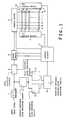
- FIG. 1is a block diagram showing an embodiment of the invention
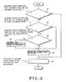
- FIG. 2is a flowchart showing the operation of a high/low luminance adjacent block detecting circuit
- FIGS. 3A to 3 Care diagrams showing high luminance blocks and low luminance blocks in an image.
- FIG. 1is a diagram showing a schematic construction of a display apparatus using a plasma display panel (hereinafter, referred to as a PDP) according to the invention.
- a PDPplasma display panel
- the display apparatuscomprises: an A/D converter 1 ; a level adjusting circuit 2 ; a control circuit 3 ; a frame memory device 4 ; an address driver 6 ; first and second sustain drivers 7 and 8 ; a PDP 10 ; an average luminance level detecting circuit 11 ; a high luminance block detecting circuit 12 ; a low luminance block detecting circuit 13 ; and a high/low luminance adjacent block detecting circuit 14 .
- the A/D converter 1samples an analog input image signal in response to a clock signal which is supplied from the control circuit 3 , converts the sampled signal into pixel data (input pixel data) D of, for example, 8 bits every pixel, and supplies it to the level adjusting circuit 2 and average luminance level detecting circuit 11 .
- the level adjusting circuit 2adjusts a luminance level of the supplied pixel data D in response to a level restriction command which is supplied from the control circuit 3 .
- the control circuit 3Synchronously with horizontal and vertical sync signals in the input image signal, the control circuit 3 generates a clock signal to the A/D converter 1 and write/read signals to the frame memory device 4 . Further, synchronously with the horizontal and vertical sync signals, the control circuit 3 generates various timing signals for driving each of the address driver 6 , first sustain driver 7 , and second sustain driver 8 .
- an adjacent block continuation detection signalwhich will be explained hereinlater, is supplied from the high/low luminance adjacent block detecting circuit 14 , the control circuit 3 generates the level restriction command to the level adjusting circuit 2 .
- the frame memory device 4sequentially writes the pixel data D supplied from the level adjusting circuit 2 into an internal memory body (not shown) in accordance with the write signal supplied from the control circuit 3 .
- the frame memory device 4divides the pixel data of one frame every bit digit, reads out the divided data from the internal memory body, and sequentially supplies them every row to the address driver 6 .
- the address driver 6generates m pixel data pulses each having a voltage corresponding to the logic level of each of the pixel data bits of one row read out from the frame memory device 4 in response to the timing signal supplied from the control circuit 3 , and applies them to column electrodes D 1 to D m of the PDP 10 , respectively.
- the PDP 10has the column electrodes D 1 to D m as address electrodes and row electrodes X 1 to X n and row electrodes Y 1 to Y n arranged so as to perpendicularly cross the column electrodes.
- row electrodes corresponding to one roware formed by a pair of row electrodes X and Y. That is, the row electrode pair of the first row in the PDP 10 is the row electrodes X 1 and Y 1 and the row electrode pair of the nth row is the row electrodes X n and Y n , respectively.
- Each of the row electrode pairs and the column electrodesis coated with a dielectric layer for a discharge space.
- a discharge cell corresponding to one pixelis formed at a cross point of each of the row electrode pairs and each of the column electrodes.
- Each of the first sustain driver 7 and the second sustain driver 8generates various driving pulses as will be explained hereinlater in response to the timing signals supplied from the control circuit 3 , and applies them to the row electrodes X 1 to X n and Y 1 to Y n of the PDP 10 .
- the average luminance level detecting circuit 11divides one frame corresponding to the screen of the PDP 10 into a predetermined number of blocks (for example, 6 blocks in the lateral direction ⁇ 5 blocks in the vertical direction), detects an average luminance level of each block on the basis of the pixel data D which is supplied from the A/D converter 1 , and generates average luminance data of each block to the high luminance block detecting circuit 12 and low luminance block detecting circuit 13 .
- the high luminance block detecting circuit 12detects a block of which an average luminance level is equal to or larger than a first reference value Th1, that is, a high luminance block from the average luminance data of each block which is supplied from the average luminance level detecting circuit 11 .
- the low luminance block detecting circuit 13detects a block of which an average luminance level is equal to or smaller than a second reference value Th2 (Th2 ⁇ Th1), that is, a low luminance block from the average luminance data of each block which is supplied from the average luminance level detecting circuit 11 .
- High luminance block data indicative of the position of the high luminance block detected by the high luminance block detecting circuit 12 and low luminance block data indicative of the position of the low luminance block detected by the low luminance block detecting circuit 13are supplied to the high/low luminance adjacent block detecting circuit 14 .
- the high/low luminance adjacent block detecting circuit 14detects the blocks in which the high luminance block and the low luminance block are adjacent to each other in the present frame in accordance with the high luminance block data and the low luminance block data, and further generates an adjacent block continuation detection signal to the control circuit 3 in the case where the adjacent blocks continue in the same state for a predetermined time.
- the blockwhen the average luminance data of an arbitrary block which is sequentially supplied from the average luminance level detecting circuit 11 is equal to or larger than the first reference value Th1, the block is detected by the high luminance block detecting circuit 12 .
- the average luminance data of an arbitrary block which is sequentially supplied from the average luminance level detecting circuit 11is equal to or smaller than the second reference value Th2, the block is detected by the low luminance block detecting circuit 13 .
- the high/low luminance adjacent block detecting circuit 14discriminates for each frame whether the adjacent blocks (block pair), which consist of a high luminance block and a low luminance block, exist or not in the detected high luminance block (blocks) and low luminance block (blocks) (step S 1 ), as shown in FIG. 2 . If the adjacent blocks in which the high luminance block and the low luminance block are neighboring mutually exist, whether the adjacent blocks have already been detected as adjacent blocks consisting of the same high luminance block and low luminance block in the previous frame or not is discriminated (step S 2 ).
- step S 3If the present detected adjacent blocks are not the adjacent blocks consisting of the same high luminance block and low luminance block in the previous frame, the positions of the adjacent blocks and the present time are stored into an internal memory (not shown) (step S 3 ). After completion of the execution in step S 3 , the positions of the adjacent blocks which do not continue in the previous and present frames and the stored time are deleted from the internal memory (step S 4 ). Step S 4 is also executed in the case where the adjacent blocks consisting of a high luminance block and a low luminance block do not exist in the present frame.
- step S 5If it is determined in step S 2 that the adjacent blocks in the present frame has already continued the state of the same high luminance block and low luminance block in the previous frame, whether the state of the same high luminance block and low luminance block has continued for a predetermined time or not is discriminated (step S 5 ).
- the continuation timeis discriminated from the time stored in the internal memory.
- the predetermined timeis set to, for example, a few seconds. If the adjacent blocks have continued the state of the same high luminance block and low luminance block for the predetermined time, the adjacent block continuation detection signal is generated to the control circuit 3 (step S 6 ).
- step S 3follows. Also after completion of the execution in step S 6 , the processing routine advances to step S 3 .
- the adjacent block continuation detection signalis generated from the high/low luminance adjacent block detecting circuit 14 .
- the control circuit 3issues a level restriction command to the level adjusting circuit 2 in response to the adjacent block continuation detection signal.
- the level adjusting circuit 2restricts the luminance level of the supplied pixel data D.
- the restricted pixel data Dis supplied to the frame memory device 4 .
- the pixel data Dis sequentially supplied to the address driver 6 .
- the PDP 10is driven by the address driver 6 , first sustain driver 7 , and second sustain driver 8 , so that an image corresponding to the input image signal is displayed by the PDP 10 .
- the display by the PDP 10if the luminance level of the pixel data D is restricted by the level adjusting circuit 2 , the large temperature difference is suppressed in the boundary portion of the high luminance block and the low luminance block, so that the deterioration of the display panel of the PDP 10 can be prevented.
- the display period of time of one fieldis divided into N subfields, the number of light emitting times corresponding to the weight of the bit digit of the pixel data (N bits) according to the input image signal is allocated every subfield, and the light emission driving is performed.
- the number of light emitting times of each subfieldcan be also reduced in response to the adjacent block continuation detection signal.
- the embodimenthas been described with respect to the example in which the invention is applied to the display apparatus using the PDP, the invention is not limited to it but can be also applied to another display apparatus using a display panel with an organic EL device.
- the luminance leveldoes not decrease unnecessarily and a situation that the frame is darkened due to the luminance restriction as in the conventional apparatus can be prevented.
Landscapes
- Engineering & Computer Science (AREA)
- Physics & Mathematics (AREA)
- Power Engineering (AREA)
- Plasma & Fusion (AREA)
- Computer Hardware Design (AREA)
- General Physics & Mathematics (AREA)
- Theoretical Computer Science (AREA)
- Control Of Indicators Other Than Cathode Ray Tubes (AREA)
- Control Of Gas Discharge Display Tubes (AREA)
- Transforming Electric Information Into Light Information (AREA)
- Controls And Circuits For Display Device (AREA)
Abstract
Description
Claims (3)
Applications Claiming Priority (2)
| Application Number | Priority Date | Filing Date | Title |
|---|---|---|---|
| JP2001-174062 | 2001-06-08 | ||
| JP2001174062AJP4610793B2 (en) | 2001-06-08 | 2001-06-08 | Display apparatus and method |
Publications (2)
| Publication Number | Publication Date |
|---|---|
| US20020195957A1 US20020195957A1 (en) | 2002-12-26 |
| US6617797B2true US6617797B2 (en) | 2003-09-09 |
Family
ID=19015403
Family Applications (1)
| Application Number | Title | Priority Date | Filing Date |
|---|---|---|---|
| US10/150,970Expired - Fee RelatedUS6617797B2 (en) | 2001-06-08 | 2002-05-21 | Display apparatus and display method |
Country Status (3)
| Country | Link |
|---|---|
| US (1) | US6617797B2 (en) |
| EP (1) | EP1265213A3 (en) |
| JP (1) | JP4610793B2 (en) |
Cited By (9)
| Publication number | Priority date | Publication date | Assignee | Title |
|---|---|---|---|---|
| US20030210256A1 (en)* | 2002-03-25 | 2003-11-13 | Yukio Mori | Display method and display apparatus |
| US20040239698A1 (en)* | 2003-03-31 | 2004-12-02 | Fujitsu Display Technologies Corporation | Image processing method and liquid-crystal display device using the same |
| US20050200291A1 (en)* | 2004-02-24 | 2005-09-15 | Naugler W. E.Jr. | Method and device for reading display pixel emission and ambient luminance levels |
| US20060007250A1 (en)* | 2004-05-25 | 2006-01-12 | Byoung-Hwa Jung | Display apparatus and control method thereof |
| US20080007494A1 (en)* | 2006-06-30 | 2008-01-10 | Lg.Philips Lcd Co., Ltd. | Organic light emitting diode display device and driving method thereof |
| US20080130750A1 (en)* | 2006-12-01 | 2008-06-05 | Samsung Electronics Co., Ltd. | Illumination compensation method and apparatus and video encoding and decoding method and apparatus using the illumination compensation method |
| US20080170014A1 (en)* | 2007-01-15 | 2008-07-17 | Jin Woung Jung | Organic light emitting display and method of correcting images thereof |
| US20100309099A1 (en)* | 2009-06-05 | 2010-12-09 | Woung Kim | Display device and driving method thereof |
| US20110037785A1 (en)* | 2008-06-27 | 2011-02-17 | Sharp Kabushiki Kaisha | Control device for liquid crystal display device, liquid crystal display device, method for controlling liquid crystal display devicde, program, and storage medium |
Families Citing this family (8)
| Publication number | Priority date | Publication date | Assignee | Title |
|---|---|---|---|---|
| US7277076B2 (en)* | 2002-12-27 | 2007-10-02 | Sharp Kabushiki Kaisha | Method of driving a display, display, and computer program therefor |
| DE10320300A1 (en)* | 2003-05-07 | 2004-12-02 | Grundig Aktiengesellschaft | Method and device for improving the gray value resolution of a pulse width controlled image display device |
| JP2005315956A (en)* | 2004-04-27 | 2005-11-10 | Pioneer Electronic Corp | Display unit driving device and driving method therefor |
| KR20050115008A (en)* | 2004-06-03 | 2005-12-07 | 엘지전자 주식회사 | Device and method for driving plasma display panel |
| KR100585527B1 (en)* | 2004-07-02 | 2006-06-07 | 엘지전자 주식회사 | Driving apparatus and driving method of plasma display panel |
| JP5137325B2 (en)* | 2006-04-27 | 2013-02-06 | 株式会社日立製作所 | Plasma display device and processing method thereof |
| JP5304211B2 (en)* | 2008-12-11 | 2013-10-02 | ソニー株式会社 | Display device, brightness adjusting device, backlight device, brightness adjusting method and program |
| KR20230065423A (en)* | 2021-11-04 | 2023-05-12 | 삼성디스플레이 주식회사 | Display device |
Citations (5)
| Publication number | Priority date | Publication date | Assignee | Title |
|---|---|---|---|---|
| US5724053A (en)* | 1994-09-07 | 1998-03-03 | Pioneer Electronic Corporation | Plasma display apparatus adapted to multiple frequencies |
| US6340961B1 (en)* | 1997-10-16 | 2002-01-22 | Nec Corporation | Method and apparatus for displaying moving images while correcting false moving image contours |
| US6396508B1 (en)* | 1999-12-02 | 2002-05-28 | Matsushita Electronics Corp. | Dynamic low-level enhancement and reduction of moving picture disturbance for a digital display |
| US6476824B1 (en)* | 1998-08-05 | 2002-11-05 | Mitsubishi Denki Kabushiki Kaisha | Luminance resolution enhancement circuit and display apparatus using same |
| US6496165B1 (en)* | 1999-07-01 | 2002-12-17 | Pioneer Corporation | Driving apparatus for driving a plasma display panel based on power consumed during a non-light emitting period of a unit display period |
Family Cites Families (4)
| Publication number | Priority date | Publication date | Assignee | Title |
|---|---|---|---|---|
| JP3455265B2 (en)* | 1994-01-25 | 2003-10-14 | パイオニア株式会社 | Driving circuit and driving method for flat display device |
| JP3636573B2 (en)* | 1997-06-27 | 2005-04-06 | パイオニア株式会社 | Brightness control device |
| JP3642170B2 (en)* | 1998-02-02 | 2005-04-27 | 三菱電機株式会社 | Plasma display panel temperature control method and plasma display apparatus |
| DE19832261A1 (en)* | 1998-07-17 | 2000-01-20 | Thomson Brandt Gmbh | Arrangement for regulating the luminance |
- 2001
- 2001-06-08JPJP2001174062Apatent/JP4610793B2/ennot_activeExpired - Fee Related
- 2002
- 2002-05-15EPEP02010878Apatent/EP1265213A3/ennot_activeWithdrawn
- 2002-05-21USUS10/150,970patent/US6617797B2/ennot_activeExpired - Fee Related
Patent Citations (5)
| Publication number | Priority date | Publication date | Assignee | Title |
|---|---|---|---|---|
| US5724053A (en)* | 1994-09-07 | 1998-03-03 | Pioneer Electronic Corporation | Plasma display apparatus adapted to multiple frequencies |
| US6340961B1 (en)* | 1997-10-16 | 2002-01-22 | Nec Corporation | Method and apparatus for displaying moving images while correcting false moving image contours |
| US6476824B1 (en)* | 1998-08-05 | 2002-11-05 | Mitsubishi Denki Kabushiki Kaisha | Luminance resolution enhancement circuit and display apparatus using same |
| US6496165B1 (en)* | 1999-07-01 | 2002-12-17 | Pioneer Corporation | Driving apparatus for driving a plasma display panel based on power consumed during a non-light emitting period of a unit display period |
| US6396508B1 (en)* | 1999-12-02 | 2002-05-28 | Matsushita Electronics Corp. | Dynamic low-level enhancement and reduction of moving picture disturbance for a digital display |
Cited By (18)
| Publication number | Priority date | Publication date | Assignee | Title |
|---|---|---|---|---|
| US20030210256A1 (en)* | 2002-03-25 | 2003-11-13 | Yukio Mori | Display method and display apparatus |
| US7139008B2 (en)* | 2002-03-25 | 2006-11-21 | Sanyo Electric Co., Ltd. | Display method and display apparatus |
| US20040239698A1 (en)* | 2003-03-31 | 2004-12-02 | Fujitsu Display Technologies Corporation | Image processing method and liquid-crystal display device using the same |
| US8502762B2 (en) | 2003-03-31 | 2013-08-06 | Sharp Kabushiki Kaisha | Image processing method and liquid-crystal display device using the same |
| US8094143B2 (en)* | 2003-03-31 | 2012-01-10 | Sharp Kabushiki Kaisha | Image processing method and liquid-crystal display device using the same |
| US20100103206A1 (en)* | 2003-03-31 | 2010-04-29 | Sharp Kabushiki Kaisha | Image processing method and liquid-crystal display device using the same |
| US20100090938A1 (en)* | 2003-03-31 | 2010-04-15 | Sharp Kabushiki Kaisha | Image processing method and liquid-crystal display device using the same |
| US20050200291A1 (en)* | 2004-02-24 | 2005-09-15 | Naugler W. E.Jr. | Method and device for reading display pixel emission and ambient luminance levels |
| US7605780B2 (en)* | 2004-05-25 | 2009-10-20 | Samsung Electronics Co., Ltd. | Display apparatus and control method thereof |
| US20060007250A1 (en)* | 2004-05-25 | 2006-01-12 | Byoung-Hwa Jung | Display apparatus and control method thereof |
| US7978159B2 (en)* | 2006-06-30 | 2011-07-12 | Lg Display Co., Ltd. | Organic light emitting diode display device and driving method thereof |
| US20080007494A1 (en)* | 2006-06-30 | 2008-01-10 | Lg.Philips Lcd Co., Ltd. | Organic light emitting diode display device and driving method thereof |
| US20080130750A1 (en)* | 2006-12-01 | 2008-06-05 | Samsung Electronics Co., Ltd. | Illumination compensation method and apparatus and video encoding and decoding method and apparatus using the illumination compensation method |
| US8774282B2 (en)* | 2006-12-01 | 2014-07-08 | Samsung Electronics Co., Ltd. | Illumination compensation method and apparatus and video encoding and decoding method and apparatus using the illumination compensation method |
| US20080170014A1 (en)* | 2007-01-15 | 2008-07-17 | Jin Woung Jung | Organic light emitting display and method of correcting images thereof |
| US20110037785A1 (en)* | 2008-06-27 | 2011-02-17 | Sharp Kabushiki Kaisha | Control device for liquid crystal display device, liquid crystal display device, method for controlling liquid crystal display devicde, program, and storage medium |
| US8917293B2 (en)* | 2008-06-27 | 2014-12-23 | Sharp Kabushiki Kaisha | Control device for liquid crystal display device, liquid crystal display device, method for controlling liquid crystal display device, program, and storage medium |
| US20100309099A1 (en)* | 2009-06-05 | 2010-12-09 | Woung Kim | Display device and driving method thereof |
Also Published As
| Publication number | Publication date |
|---|---|
| EP1265213A3 (en) | 2005-04-20 |
| US20020195957A1 (en) | 2002-12-26 |
| EP1265213A2 (en) | 2002-12-11 |
| JP4610793B2 (en) | 2011-01-12 |
| JP2002366087A (en) | 2002-12-20 |
Similar Documents
| Publication | Publication Date | Title |
|---|---|---|
| US6617797B2 (en) | Display apparatus and display method | |
| US6465970B2 (en) | Plasma display panel driving method | |
| US6278422B1 (en) | Method of driving plasma display panel and display apparatus | |
| US7233300B2 (en) | Apparatus and method for displaying gray scales of plasma display panel | |
| US6717557B2 (en) | Driving apparatus and driving method of an AC type plasma display panel having auxiliary electrodes | |
| US7142175B2 (en) | Method and apparatus for displaying grayscale of plasma display panel | |
| KR20010098797A (en) | Cascade stage plasma display panel for reducing the power in writing the data | |
| US7525513B2 (en) | Method and apparatus for driving plasma display panel having operation mode selection based on motion detected | |
| US6798393B2 (en) | Plasma display device | |
| KR100603311B1 (en) | Panel driving method and device | |
| US6753831B1 (en) | Display device | |
| JP2002023694A (en) | Multi-tone image display device with reduced power consumption during data writing | |
| US6999047B1 (en) | Displaying video on a plasma display panel | |
| KR100271132B1 (en) | Apparatus for protesting screen and driving thereof for plasma display panel | |
| US7164398B2 (en) | Apparatus and method for driving plasma display panel, and processing program embodied in a recording medium for driving plasma display panel | |
| KR20060001406A (en) | Driving Method of Plasma Display Panel | |
| US20030038758A1 (en) | Display apparatus | |
| US20070109222A1 (en) | Plasma display device and driving method thereof | |
| KR100542212B1 (en) | Driving method of plasma display panel and apparatus thereof | |
| KR100489277B1 (en) | Method and apparatus for driving plasma display panel | |
| KR100257484B1 (en) | Plasma display panel and its control method | |
| KR100573136B1 (en) | Display panel driving method and device | |
| JP2003066893A (en) | Driving method of plasma display panel | |
| KR100490627B1 (en) | Method and device for driving of plasma display panel | |
| KR100581883B1 (en) | Panel driving method and device |
Legal Events
| Date | Code | Title | Description |
|---|---|---|---|
| AS | Assignment | Owner name:PIONEER CORPORATION, JAPAN Free format text:ASSIGNMENT OF ASSIGNORS INTEREST;ASSIGNORS:HIGUCHI, YASUNORI;MOCHIZUKI, HITOSHI;REEL/FRAME:012917/0610;SIGNING DATES FROM 20020423 TO 20020425 Owner name:SHIZUOKA PIONEER CORPORATION, JAPAN Free format text:ASSIGNMENT OF ASSIGNORS INTEREST;ASSIGNORS:HIGUCHI, YASUNORI;MOCHIZUKI, HITOSHI;REEL/FRAME:012917/0610;SIGNING DATES FROM 20020423 TO 20020425 | |
| AS | Assignment | Owner name:PIONEER DISPLAY PRODUCTS CORPORATION, JAPAN Free format text:CHANGE OF NAME;ASSIGNOR:SHIZUOKA PIONEER CORPORATION;REEL/FRAME:014295/0877 Effective date:20030401 | |
| FPAY | Fee payment | Year of fee payment:4 | |
| FEPP | Fee payment procedure | Free format text:PAYOR NUMBER ASSIGNED (ORIGINAL EVENT CODE: ASPN); ENTITY STATUS OF PATENT OWNER: LARGE ENTITY | |
| AS | Assignment | Owner name:PANASONIC CORPORATION, JAPAN Free format text:ASSIGNMENT OF ASSIGNORS INTEREST;ASSIGNORS:PIONEER CORPORATION (FORMERLY CALLED PIONEER ELECTRONIC CORPORATION);PIONEER DISPLAY PRODUCTS CORPORATION (FORMERLY SHIZUOKA PIONEER ELECTRONIC CORPORATION);REEL/FRAME:023234/0158 Effective date:20090907 | |
| FPAY | Fee payment | Year of fee payment:8 | |
| REMI | Maintenance fee reminder mailed | ||
| LAPS | Lapse for failure to pay maintenance fees | ||
| STCH | Information on status: patent discontinuation | Free format text:PATENT EXPIRED DUE TO NONPAYMENT OF MAINTENANCE FEES UNDER 37 CFR 1.362 | |
| FP | Lapsed due to failure to pay maintenance fee | Effective date:20150909 |