US6617525B2 - Molded stiffener for flexible circuit molding - Google Patents
Molded stiffener for flexible circuit moldingDownload PDFInfo
- Publication number
- US6617525B2 US6617525B2US10/043,603US4360302AUS6617525B2US 6617525 B2US6617525 B2US 6617525B2US 4360302 AUS4360302 AUS 4360302AUS 6617525 B2US6617525 B2US 6617525B2
- Authority
- US
- United States
- Prior art keywords
- molded
- flexible
- stiffener
- flexible circuit
- circuit
- Prior art date
- Legal status (The legal status is an assumption and is not a legal conclusion. Google has not performed a legal analysis and makes no representation as to the accuracy of the status listed.)
- Expired - Lifetime
Links
- 239000003351stiffenerSubstances0.000titleclaimsabstractdescription46
- 238000000465mouldingMethods0.000titledescription14
- 238000005538encapsulationMethods0.000claimsabstractdescription10
- 239000000463materialSubstances0.000claimsdescription12
- 239000004642PolyimideSubstances0.000claimsdescription3
- 229920001721polyimidePolymers0.000claimsdescription3
- 239000004593EpoxySubstances0.000claims1
- 238000000034methodMethods0.000abstractdescription5
- 230000015572biosynthetic processEffects0.000abstractdescription2
- 150000001875compoundsChemical class0.000description9
- PCHJSUWPFVWCPO-UHFFFAOYSA-NgoldChemical compound[Au]PCHJSUWPFVWCPO-UHFFFAOYSA-N0.000description8
- RYGMFSIKBFXOCR-UHFFFAOYSA-NCopperChemical compound[Cu]RYGMFSIKBFXOCR-UHFFFAOYSA-N0.000description6
- 229910052802copperInorganic materials0.000description6
- 239000010949copperSubstances0.000description6
- 229910000679solderInorganic materials0.000description6
- 230000000712assemblyEffects0.000description3
- 238000000429assemblyMethods0.000description3
- 239000008393encapsulating agentSubstances0.000description3
- 238000001746injection mouldingMethods0.000description2
- 239000000853adhesiveSubstances0.000description1
- 230000001070adhesive effectEffects0.000description1
- 238000004806packaging method and processMethods0.000description1
- 239000000843powderSubstances0.000description1
- 239000004065semiconductorSubstances0.000description1
- 239000000758substrateSubstances0.000description1
Images


Classifications
- H—ELECTRICITY
- H01—ELECTRIC ELEMENTS
- H01L—SEMICONDUCTOR DEVICES NOT COVERED BY CLASS H10
- H01L23/00—Details of semiconductor or other solid state devices
- H01L23/28—Encapsulations, e.g. encapsulating layers, coatings, e.g. for protection
- H01L23/31—Encapsulations, e.g. encapsulating layers, coatings, e.g. for protection characterised by the arrangement or shape
- H01L23/3107—Encapsulations, e.g. encapsulating layers, coatings, e.g. for protection characterised by the arrangement or shape the device being completely enclosed
- H01L23/3121—Encapsulations, e.g. encapsulating layers, coatings, e.g. for protection characterised by the arrangement or shape the device being completely enclosed a substrate forming part of the encapsulation
- B—PERFORMING OPERATIONS; TRANSPORTING
- B29—WORKING OF PLASTICS; WORKING OF SUBSTANCES IN A PLASTIC STATE IN GENERAL
- B29C—SHAPING OR JOINING OF PLASTICS; SHAPING OF MATERIAL IN A PLASTIC STATE, NOT OTHERWISE PROVIDED FOR; AFTER-TREATMENT OF THE SHAPED PRODUCTS, e.g. REPAIRING
- B29C45/00—Injection moulding, i.e. forcing the required volume of moulding material through a nozzle into a closed mould; Apparatus therefor
- B29C45/14—Injection moulding, i.e. forcing the required volume of moulding material through a nozzle into a closed mould; Apparatus therefor incorporating preformed parts or layers, e.g. injection moulding around inserts or for coating articles
- B29C45/14639—Injection moulding, i.e. forcing the required volume of moulding material through a nozzle into a closed mould; Apparatus therefor incorporating preformed parts or layers, e.g. injection moulding around inserts or for coating articles for obtaining an insulating effect, e.g. for electrical components
- H—ELECTRICITY
- H01—ELECTRIC ELEMENTS
- H01L—SEMICONDUCTOR DEVICES NOT COVERED BY CLASS H10
- H01L21/00—Processes or apparatus adapted for the manufacture or treatment of semiconductor or solid state devices or of parts thereof
- H01L21/02—Manufacture or treatment of semiconductor devices or of parts thereof
- H01L21/04—Manufacture or treatment of semiconductor devices or of parts thereof the devices having potential barriers, e.g. a PN junction, depletion layer or carrier concentration layer
- H01L21/50—Assembly of semiconductor devices using processes or apparatus not provided for in a single one of the groups H01L21/18 - H01L21/326 or H10D48/04 - H10D48/07 e.g. sealing of a cap to a base of a container
- H01L21/56—Encapsulations, e.g. encapsulation layers, coatings
- H01L21/565—Moulds
- H—ELECTRICITY
- H01—ELECTRIC ELEMENTS
- H01L—SEMICONDUCTOR DEVICES NOT COVERED BY CLASS H10
- H01L23/00—Details of semiconductor or other solid state devices
- H01L23/48—Arrangements for conducting electric current to or from the solid state body in operation, e.g. leads, terminal arrangements ; Selection of materials therefor
- H01L23/488—Arrangements for conducting electric current to or from the solid state body in operation, e.g. leads, terminal arrangements ; Selection of materials therefor consisting of soldered or bonded constructions
- H01L23/498—Leads, i.e. metallisations or lead-frames on insulating substrates, e.g. chip carriers
- H01L23/4985—Flexible insulating substrates
- H—ELECTRICITY
- H01—ELECTRIC ELEMENTS
- H01L—SEMICONDUCTOR DEVICES NOT COVERED BY CLASS H10
- H01L2224/00—Indexing scheme for arrangements for connecting or disconnecting semiconductor or solid-state bodies and methods related thereto as covered by H01L24/00
- H01L2224/01—Means for bonding being attached to, or being formed on, the surface to be connected, e.g. chip-to-package, die-attach, "first-level" interconnects; Manufacturing methods related thereto
- H01L2224/42—Wire connectors; Manufacturing methods related thereto
- H01L2224/44—Structure, shape, material or disposition of the wire connectors prior to the connecting process
- H01L2224/45—Structure, shape, material or disposition of the wire connectors prior to the connecting process of an individual wire connector
- H01L2224/45001—Core members of the connector
- H01L2224/45099—Material
- H01L2224/451—Material with a principal constituent of the material being a metal or a metalloid, e.g. boron (B), silicon (Si), germanium (Ge), arsenic (As), antimony (Sb), tellurium (Te) and polonium (Po), and alloys thereof
- H01L2224/45138—Material with a principal constituent of the material being a metal or a metalloid, e.g. boron (B), silicon (Si), germanium (Ge), arsenic (As), antimony (Sb), tellurium (Te) and polonium (Po), and alloys thereof the principal constituent melting at a temperature of greater than or equal to 950°C and less than 1550°C
- H01L2224/45144—Gold (Au) as principal constituent
- H—ELECTRICITY
- H01—ELECTRIC ELEMENTS
- H01L—SEMICONDUCTOR DEVICES NOT COVERED BY CLASS H10
- H01L2224/00—Indexing scheme for arrangements for connecting or disconnecting semiconductor or solid-state bodies and methods related thereto as covered by H01L24/00
- H01L2224/01—Means for bonding being attached to, or being formed on, the surface to be connected, e.g. chip-to-package, die-attach, "first-level" interconnects; Manufacturing methods related thereto
- H01L2224/42—Wire connectors; Manufacturing methods related thereto
- H01L2224/47—Structure, shape, material or disposition of the wire connectors after the connecting process
- H01L2224/48—Structure, shape, material or disposition of the wire connectors after the connecting process of an individual wire connector
- H01L2224/4805—Shape
- H01L2224/4809—Loop shape
- H01L2224/48091—Arched
- H—ELECTRICITY
- H01—ELECTRIC ELEMENTS
- H01L—SEMICONDUCTOR DEVICES NOT COVERED BY CLASS H10
- H01L2224/00—Indexing scheme for arrangements for connecting or disconnecting semiconductor or solid-state bodies and methods related thereto as covered by H01L24/00
- H01L2224/01—Means for bonding being attached to, or being formed on, the surface to be connected, e.g. chip-to-package, die-attach, "first-level" interconnects; Manufacturing methods related thereto
- H01L2224/42—Wire connectors; Manufacturing methods related thereto
- H01L2224/47—Structure, shape, material or disposition of the wire connectors after the connecting process
- H01L2224/48—Structure, shape, material or disposition of the wire connectors after the connecting process of an individual wire connector
- H01L2224/481—Disposition
- H01L2224/48151—Connecting between a semiconductor or solid-state body and an item not being a semiconductor or solid-state body, e.g. chip-to-substrate, chip-to-passive
- H01L2224/48221—Connecting between a semiconductor or solid-state body and an item not being a semiconductor or solid-state body, e.g. chip-to-substrate, chip-to-passive the body and the item being stacked
- H01L2224/48225—Connecting between a semiconductor or solid-state body and an item not being a semiconductor or solid-state body, e.g. chip-to-substrate, chip-to-passive the body and the item being stacked the item being non-metallic, e.g. insulating substrate with or without metallisation
- H01L2224/48227—Connecting between a semiconductor or solid-state body and an item not being a semiconductor or solid-state body, e.g. chip-to-substrate, chip-to-passive the body and the item being stacked the item being non-metallic, e.g. insulating substrate with or without metallisation connecting the wire to a bond pad of the item
- H01L2224/48228—Connecting between a semiconductor or solid-state body and an item not being a semiconductor or solid-state body, e.g. chip-to-substrate, chip-to-passive the body and the item being stacked the item being non-metallic, e.g. insulating substrate with or without metallisation connecting the wire to a bond pad of the item the bond pad being disposed in a recess of the surface of the item
- H—ELECTRICITY
- H01—ELECTRIC ELEMENTS
- H01L—SEMICONDUCTOR DEVICES NOT COVERED BY CLASS H10
- H01L24/00—Arrangements for connecting or disconnecting semiconductor or solid-state bodies; Methods or apparatus related thereto
- H01L24/01—Means for bonding being attached to, or being formed on, the surface to be connected, e.g. chip-to-package, die-attach, "first-level" interconnects; Manufacturing methods related thereto
- H01L24/42—Wire connectors; Manufacturing methods related thereto
- H01L24/44—Structure, shape, material or disposition of the wire connectors prior to the connecting process
- H01L24/45—Structure, shape, material or disposition of the wire connectors prior to the connecting process of an individual wire connector
- H—ELECTRICITY
- H01—ELECTRIC ELEMENTS
- H01L—SEMICONDUCTOR DEVICES NOT COVERED BY CLASS H10
- H01L24/00—Arrangements for connecting or disconnecting semiconductor or solid-state bodies; Methods or apparatus related thereto
- H01L24/01—Means for bonding being attached to, or being formed on, the surface to be connected, e.g. chip-to-package, die-attach, "first-level" interconnects; Manufacturing methods related thereto
- H01L24/42—Wire connectors; Manufacturing methods related thereto
- H01L24/47—Structure, shape, material or disposition of the wire connectors after the connecting process
- H01L24/48—Structure, shape, material or disposition of the wire connectors after the connecting process of an individual wire connector
- H—ELECTRICITY
- H01—ELECTRIC ELEMENTS
- H01L—SEMICONDUCTOR DEVICES NOT COVERED BY CLASS H10
- H01L2924/00—Indexing scheme for arrangements or methods for connecting or disconnecting semiconductor or solid-state bodies as covered by H01L24/00
- H01L2924/01—Chemical elements
- H01L2924/01013—Aluminum [Al]
- H—ELECTRICITY
- H01—ELECTRIC ELEMENTS
- H01L—SEMICONDUCTOR DEVICES NOT COVERED BY CLASS H10
- H01L2924/00—Indexing scheme for arrangements or methods for connecting or disconnecting semiconductor or solid-state bodies as covered by H01L24/00
- H01L2924/01—Chemical elements
- H01L2924/01079—Gold [Au]
- H—ELECTRICITY
- H01—ELECTRIC ELEMENTS
- H01L—SEMICONDUCTOR DEVICES NOT COVERED BY CLASS H10
- H01L2924/00—Indexing scheme for arrangements or methods for connecting or disconnecting semiconductor or solid-state bodies as covered by H01L24/00
- H01L2924/10—Details of semiconductor or other solid state devices to be connected
- H01L2924/11—Device type
- H01L2924/14—Integrated circuits
- H—ELECTRICITY
- H01—ELECTRIC ELEMENTS
- H01L—SEMICONDUCTOR DEVICES NOT COVERED BY CLASS H10
- H01L2924/00—Indexing scheme for arrangements or methods for connecting or disconnecting semiconductor or solid-state bodies as covered by H01L24/00
- H01L2924/15—Details of package parts other than the semiconductor or other solid state devices to be connected
- H01L2924/151—Die mounting substrate
- H01L2924/153—Connection portion
- H01L2924/1531—Connection portion the connection portion being formed only on the surface of the substrate opposite to the die mounting surface
- H01L2924/15311—Connection portion the connection portion being formed only on the surface of the substrate opposite to the die mounting surface being a ball array, e.g. BGA
- H—ELECTRICITY
- H01—ELECTRIC ELEMENTS
- H01L—SEMICONDUCTOR DEVICES NOT COVERED BY CLASS H10
- H01L2924/00—Indexing scheme for arrangements or methods for connecting or disconnecting semiconductor or solid-state bodies as covered by H01L24/00
- H01L2924/15—Details of package parts other than the semiconductor or other solid state devices to be connected
- H01L2924/181—Encapsulation
Definitions
- This inventionrelates to the formation of molded stiffeners which are formed at the same time molded circuit elements are formed.
- molded flexible circuit assembliesrequire the use of stiffeners to provide adequate rigidity of the flexible assembly during processing.
- This inventiondescribes the use of a molded stiffener to accomplish the required rigidity.
- U.S. Pat. No. 5,635,671 to Freyman et al.describes encapsulation of an electronic device using injection molding with a two piece mold using a degating region having a material chosen such that the material in the degating region forms a weak bond with the encapsulant used.
- U.S. Pat. No. 5,506,756 to Haleydescribes a ball grid array package containing an integrated circuit die that is directly mounted to either a heat sink or a printed circuit board.
- U.S. Pat. No. 5,241,133 to Mullen, III et al.describes a leadless pad array chip carrier package.
- a semiconductor deviceis electrically wire bonded and attached with conductive adhesive to a metallized pattern on a printed circuit board.
- Flexible circuitsare frequently used in electronic circuit packaging. Molded flexible circuit elements are formed on a flexible tape so that several such circuit elements can be processed simultaneously for such operations as electronic chip attachment, wire bond attachment, and encapsulation. Stiffeners are required to provide adequate rigidity to the flexible circuits for these processing operations.
- FIGS. 1 and 2show a number of flexible circuit elements 12 formed on a flexible tape 10 .
- the detail of the circuit elements 12is not shown here but the circuit elements typically include a die in a molded encapsulation.
- a stiffener 14is attached to the assembly to provide rigidity during the processing operations. These flexible circuit assemblies must use a stiffener 14 to add rigidity during these processing operations and this stiffener which must be removed at the last operation of the process, adding cost and complexity.
- the mold sectionincludes circuit element cavities, a stiffener cavity, mold runner cavities, and a molding compound cull block. Uncured molding compound is placed in the molding compound cull block and flowed through the mold runner cavities into the circuit element cavities and the stiffener cavity. The molding compound is cured and the mold section removed leaving molded circuit elements and stiffeners formed on the flexible tape.
- the molded circuit elementswhich will be explained in more detail later, include a circuit die and wiring.
- the molded stiffenersprovide adequate stiffening for subsequent processing operations and no additional stiffeners are required.
- the molded stiffenerscan be used in the processing and are removed when the molded circuit elements are removed from the flexible tape.
- FIG. 1shows a top view of a conventional flexible circuit assembly with a stiffener attached.
- FIG. 2shows a cross section view of a conventional flexible circuit assembly with a stiffener attached.
- FIG. 3shows a bottom view of a mold section used to form the flexible circuit assembly with stiffeners of this invention.
- FIG. 4shows a top view of the flexible circuit assembly with a molded stiffener of this invention.
- FIG. 5shows a cross section view of the flexible circuit assembly with a molded stiffener of FIG. 4 along line 5 - 5 ′ of FIG. 4 .
- FIG. 6shows a cross section view of the flexible circuit assembly with a molded stiffener of FIG. 4 along line 6 - 6 ′ of FIG. 4 .
- FIG. 7shows a cross section view of a first example of a circuit element on a flexible tape.
- FIG. 8shows a cross section view of a second example of a circuit element on a flexible tape.
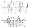
- FIG. 3shows a bottom view of a mold section 25 which will be used to mold circuit elements and stiffeners for the molded flexible circuit assembly.
- the mold section 25has a molding compound cull block 21 , a first mold runner cavity 19 , a stiffener cavity 17 , second mold runner gate cavities 15 , and circuit element cavities 11 .
- the molding compoundis a material such as a compacted powder in a semicured state which is later cured using time and temperature.
- the molding compoundis then cured using time and temperature, such as between about 125° C. and 190° C. for between about one and two minutes.
- the mold sectionis then removed leaving cured molding compound to form a first mold runner 20 , a stiffener 18 , second mold runners 16 , and molded circuit elements 12 formed on the flexible tape 10 .
- Any cured molding compound residue, and any part of the first mold runner 20 not on the flexible tape 10is removed after the molding is completed.
- FIGS. 4 and 5show an example of a mold section 25 providing two circuit elements 12 each, however mold sections having a larger or smaller number of circuit elements, for example one, three, four, or more, can also be used.
- the mold sectioncan be used to repeat the pattern of circuit elements any number of times on the flexible tape 10 desired or needed.
- Molded circuit elements 12 and stiffeners 18are formed on the flexible tape 10 .
- the stiffeners 18provide rigidity to the molded flexible circuit assembly and no additional stiffeners are required.
- the molded circuit elements 12have circuit dies attached, have wiring attached to the circuit dies, and can have via holes formed in the flexible tape depending on the needs of a particular circuit element design.
- the flexible circuit assemblieshave sufficient rigidity supplied by the molded stiffeners 18 for subsequent processing operations such as forming wiring traces on the first or second surfaces of the flexible tape 10 or attachment of circuit dies to the flexible tape 10 .
- FIG. 4shows four molded circuit elements 12 on a segment of the flexible tape 10 however more or fewer molded circuit elements 12 and be formed on a segment of flexible tape 10 and processed as a group.
- FIG. 5shows a cross section of the flexible circuit assembly along the line 5 - 5 ′ of FIG. 4 showing molded circuit elements 12 on a segment of flexible tape 10 with no additional stiffener attached to the flexible tape 10 .
- FIG. 5does not show the wiring and circuit dies of the molded circuit elements.
- FIGS. 7 and 8show more detail of examples of molded circuit elements and will be described later.
- FIG. 6shows a cross section of the flexible circuit assembly along the line 6 - 6 ′ of FIG. 4 showing a molded stiffener 18 on a segment of flexible tape 10 with no additional stiffener attached to the flexible tape 10 .
- the molded stiffeners 18are formed at the same time the mold runners and molded circuit elements 12 are formed and do not add any processing steps or complexity.
- the molded stiffeners 18can be removed from the molded circuit elements 12 at the same time the mold runners are removed after the processing of the molded circuit elements has been completed. The removal of the molded stiffeners 18 does not add any processing steps or complexity to the removal of the mold runners, since the final package form does not normally include mold runners.
- FIG. 7shows a first example of a molded circuit element 12 having a circuit die 30 attached to the flexible tape 10 .
- the flexible tape 10is a flexible material such as polyimide or the like. Copper pads 34 are formed on the opposite side of the flexible tape from the circuit die 30 . Wire bonds using a material such as gold wire 32 are bonded to the circuit die 30 and to the copper pads 34 through via holes 40 in the flexible tape 10 . Solder balls 36 are attached to the copper pads 34 through a solder mask 38 formed of a material not wettable by the solder.
- the circuit die 30 and gold wire 32are encapsulated in a molded encapsulant 42 using the molding process described earlier.
- FIG. 8shows a second example of a molded circuit element 12 having a circuit die 30 attached to the flexible tape 10 .
- the flexible tape 10is a flexible material such as polyimide or the like.
- Via holes 41is formed in the flexible tape 10 and copper pads 35 are formed on both sides and in the via holes 41 of the flexible tape 10 .
- Wire bonds using a material such as gold wire 32are bonded to the circuit die 30 and to the copper pads 35 .
- Solder balls 36are attached to the copper pads 35 through a solder mask 39 formed of a material not wettable by the solder.
- the circuit die 30 and gold wire 32are encapsulated in a molded encapsulant 42 using the molding process described earlier.
Landscapes
- Engineering & Computer Science (AREA)
- Microelectronics & Electronic Packaging (AREA)
- Physics & Mathematics (AREA)
- Condensed Matter Physics & Semiconductors (AREA)
- General Physics & Mathematics (AREA)
- Computer Hardware Design (AREA)
- Power Engineering (AREA)
- Manufacturing & Machinery (AREA)
- Mechanical Engineering (AREA)
- Moulds For Moulding Plastics Or The Like (AREA)
Abstract
Description
Claims (6)
Priority Applications (1)
| Application Number | Priority Date | Filing Date | Title |
|---|---|---|---|
| US10/043,603US6617525B2 (en) | 1999-02-12 | 2002-01-14 | Molded stiffener for flexible circuit molding |
Applications Claiming Priority (2)
| Application Number | Priority Date | Filing Date | Title |
|---|---|---|---|
| US09/249,251US6355199B1 (en) | 1999-02-12 | 1999-02-12 | Method of molding flexible circuit with molded stiffener |
| US10/043,603US6617525B2 (en) | 1999-02-12 | 2002-01-14 | Molded stiffener for flexible circuit molding |
Related Parent Applications (1)
| Application Number | Title | Priority Date | Filing Date |
|---|---|---|---|
| US09/249,251DivisionUS6355199B1 (en) | 1999-02-12 | 1999-02-12 | Method of molding flexible circuit with molded stiffener |
Publications (2)
| Publication Number | Publication Date |
|---|---|
| US20020056570A1 US20020056570A1 (en) | 2002-05-16 |
| US6617525B2true US6617525B2 (en) | 2003-09-09 |
Family
ID=22942651
Family Applications (2)
| Application Number | Title | Priority Date | Filing Date |
|---|---|---|---|
| US09/249,251Expired - LifetimeUS6355199B1 (en) | 1999-02-12 | 1999-02-12 | Method of molding flexible circuit with molded stiffener |
| US10/043,603Expired - LifetimeUS6617525B2 (en) | 1999-02-12 | 2002-01-14 | Molded stiffener for flexible circuit molding |
Family Applications Before (1)
| Application Number | Title | Priority Date | Filing Date |
|---|---|---|---|
| US09/249,251Expired - LifetimeUS6355199B1 (en) | 1999-02-12 | 1999-02-12 | Method of molding flexible circuit with molded stiffener |
Country Status (2)
| Country | Link |
|---|---|
| US (2) | US6355199B1 (en) |
| SG (2) | SG108836A1 (en) |
Cited By (3)
| Publication number | Priority date | Publication date | Assignee | Title |
|---|---|---|---|---|
| US20060093259A1 (en)* | 2003-12-30 | 2006-05-04 | International Business Machines Corporation | Electro-Optical Module Comprising Flexible Connection Cable and Method of Making the Same |
| US20080069494A1 (en)* | 2004-11-02 | 2008-03-20 | International Business Machines Corporation | Electro-optical module comprising flexible connection cable and method of making the same |
| US20090107630A1 (en)* | 2007-10-24 | 2009-04-30 | International Business Machines Corporation | Mechanically decoupled opto-mechanical connector for flexible optical waveguides embedded and/or attached to a printed circuit board |
Families Citing this family (14)
| Publication number | Priority date | Publication date | Assignee | Title |
|---|---|---|---|---|
| EP2298728A1 (en)* | 1998-11-12 | 2011-03-23 | Life Technologies Corporation | Transfection reagents |
| US6523254B1 (en)* | 2000-04-19 | 2003-02-25 | Micron Technology, Inc. | Method for gate blocking x-outs during a molding process |
| FR2809229B1 (en)* | 2000-05-22 | 2002-12-13 | St Microelectronics Sa | ANTI-BURRY INJECTION MOLD OF AN ENCAPSULATION MATERIAL OF A CHIP OF INTEGRATED CIRCUITS |
| US6812552B2 (en)* | 2002-04-29 | 2004-11-02 | Advanced Interconnect Technologies Limited | Partially patterned lead frames and methods of making and using the same in semiconductor packaging |
| US8236612B2 (en)* | 2002-04-29 | 2012-08-07 | Unisem (Mauritius) Holdings Limited | Partially patterned lead frames and methods of making and using the same in semiconductor packaging |
| US7799611B2 (en)* | 2002-04-29 | 2010-09-21 | Unisem (Mauritius) Holdings Limited | Partially patterned lead frames and methods of making and using the same in semiconductor packaging |
| US20040058478A1 (en)* | 2002-09-25 | 2004-03-25 | Shafidul Islam | Taped lead frames and methods of making and using the same in semiconductor packaging |
| US20040214371A1 (en)* | 2003-04-25 | 2004-10-28 | Mahmood Syed Omar Syed | System and method for conventional molding using a new design potblock |
| TW591773B (en)* | 2003-08-12 | 2004-06-11 | Advanced Semiconductor Eng | Mold and method for molding semiconductor devices |
| US7061085B2 (en)* | 2003-09-19 | 2006-06-13 | Micron Technology, Inc. | Semiconductor component and system having stiffener and circuit decal |
| US20060055691A1 (en)* | 2004-09-11 | 2006-03-16 | Bursett Jeffrey M | Attachable informational appliance |
| US20070120240A1 (en)* | 2005-11-29 | 2007-05-31 | 3M Innovative Properties Company | Circuit substrate and method of manufacture |
| CN101601133B (en)* | 2006-10-27 | 2011-08-10 | 宇芯(毛里求斯)控股有限公司 | Partially patterned leadframe and methods of making and using same in semiconductor package |
| US7998797B2 (en)* | 2008-12-09 | 2011-08-16 | Infineon Technologies Ag | Semiconductor device |
Citations (10)
| Publication number | Priority date | Publication date | Assignee | Title |
|---|---|---|---|---|
| US5241133A (en) | 1990-12-21 | 1993-08-31 | Motorola, Inc. | Leadless pad array chip carrier |
| US5355283A (en)* | 1993-04-14 | 1994-10-11 | Amkor Electronics, Inc. | Ball grid array with via interconnection |
| US5397921A (en)* | 1993-09-03 | 1995-03-14 | Advanced Semiconductor Assembly Technology | Tab grid array |
| US5506756A (en) | 1994-01-25 | 1996-04-09 | Intel Corporation | Tape BGA package die-up/die down |
| US5635671A (en) | 1994-03-16 | 1997-06-03 | Amkor Electronics, Inc. | Mold runner removal from a substrate-based packaged electronic device |
| US5835355A (en)* | 1997-09-22 | 1998-11-10 | Lsi Logic Corporation | Tape ball grid array package with perforated metal stiffener |
| US5859475A (en)* | 1996-04-24 | 1999-01-12 | Amkor Technology, Inc. | Carrier strip and molded flex circuit ball grid array |
| US5888849A (en)* | 1997-04-07 | 1999-03-30 | International Business Machines Corporation | Method for fabricating an electronic package |
| US5901041A (en)* | 1997-12-02 | 1999-05-04 | Northern Telecom Limited | Flexible integrated circuit package |
| US6326544B1 (en)* | 1996-02-05 | 2001-12-04 | Micron Technology, Inc. | Polymer based circuit |
Family Cites Families (6)
| Publication number | Priority date | Publication date | Assignee | Title |
|---|---|---|---|---|
| US3797138A (en)* | 1973-03-02 | 1974-03-19 | A Closson | Foamed sheet for making stiffening elements |
| US5760465A (en)* | 1996-02-01 | 1998-06-02 | International Business Machines Corporation | Electronic package with strain relief means |
| US5852870A (en)* | 1996-04-24 | 1998-12-29 | Amkor Technology, Inc. | Method of making grid array assembly |
| CA2180807C (en)* | 1996-07-09 | 2002-11-05 | Lynda Boutin | Integrated circuit chip package and encapsulation process |
| US5882459A (en)* | 1996-11-08 | 1999-03-16 | W. L. Gore & Associates, Inc. | Method for aligning and laminating substrates to stiffeners in electrical circuits |
| US5868887A (en)* | 1996-11-08 | 1999-02-09 | W. L. Gore & Associates, Inc. | Method for minimizing warp and die stress in the production of an electronic assembly |
- 1999
- 1999-02-12USUS09/249,251patent/US6355199B1/ennot_activeExpired - Lifetime
- 1999-06-30SGSG200201106Apatent/SG108836A1/enunknown
- 1999-06-30SGSG9903190Apatent/SG89285A1/enunknown
- 2002
- 2002-01-14USUS10/043,603patent/US6617525B2/ennot_activeExpired - Lifetime
Patent Citations (10)
| Publication number | Priority date | Publication date | Assignee | Title |
|---|---|---|---|---|
| US5241133A (en) | 1990-12-21 | 1993-08-31 | Motorola, Inc. | Leadless pad array chip carrier |
| US5355283A (en)* | 1993-04-14 | 1994-10-11 | Amkor Electronics, Inc. | Ball grid array with via interconnection |
| US5397921A (en)* | 1993-09-03 | 1995-03-14 | Advanced Semiconductor Assembly Technology | Tab grid array |
| US5506756A (en) | 1994-01-25 | 1996-04-09 | Intel Corporation | Tape BGA package die-up/die down |
| US5635671A (en) | 1994-03-16 | 1997-06-03 | Amkor Electronics, Inc. | Mold runner removal from a substrate-based packaged electronic device |
| US6326544B1 (en)* | 1996-02-05 | 2001-12-04 | Micron Technology, Inc. | Polymer based circuit |
| US5859475A (en)* | 1996-04-24 | 1999-01-12 | Amkor Technology, Inc. | Carrier strip and molded flex circuit ball grid array |
| US5888849A (en)* | 1997-04-07 | 1999-03-30 | International Business Machines Corporation | Method for fabricating an electronic package |
| US5835355A (en)* | 1997-09-22 | 1998-11-10 | Lsi Logic Corporation | Tape ball grid array package with perforated metal stiffener |
| US5901041A (en)* | 1997-12-02 | 1999-05-04 | Northern Telecom Limited | Flexible integrated circuit package |
Cited By (6)
| Publication number | Priority date | Publication date | Assignee | Title |
|---|---|---|---|---|
| US20060093259A1 (en)* | 2003-12-30 | 2006-05-04 | International Business Machines Corporation | Electro-Optical Module Comprising Flexible Connection Cable and Method of Making the Same |
| US7389012B2 (en)* | 2003-12-30 | 2008-06-17 | International Business Machines Corporation | Electro-optical module comprising flexible connection cable and method of making the same |
| US20080069494A1 (en)* | 2004-11-02 | 2008-03-20 | International Business Machines Corporation | Electro-optical module comprising flexible connection cable and method of making the same |
| US7382946B2 (en)* | 2004-11-02 | 2008-06-03 | International Business Machines Corporation | Electro-optical module comprising flexible connection cable and method of making the same |
| US20090107630A1 (en)* | 2007-10-24 | 2009-04-30 | International Business Machines Corporation | Mechanically decoupled opto-mechanical connector for flexible optical waveguides embedded and/or attached to a printed circuit board |
| US7794561B2 (en)* | 2007-10-24 | 2010-09-14 | International Business Machines Corporation | Mechanically decoupled opto-mechanical connector for flexible optical waveguides embedded and/or attached to a printed circuit board |
Also Published As
| Publication number | Publication date |
|---|---|
| US20020056570A1 (en) | 2002-05-16 |
| SG108836A1 (en) | 2005-02-28 |
| SG89285A1 (en) | 2002-06-18 |
| US6355199B1 (en) | 2002-03-12 |
Similar Documents
| Publication | Publication Date | Title |
|---|---|---|
| US6617525B2 (en) | Molded stiffener for flexible circuit molding | |
| US10468344B2 (en) | Method of manufacturing semiconductor devices and corresponding product | |
| US7112048B2 (en) | BOC BGA package for die with I-shaped bond pad layout | |
| US6664616B2 (en) | Semiconductor device and manufacturing method thereof | |
| KR100280762B1 (en) | Thermally Reinforced Semiconductor Devices Having Exposed Backsides and Methods of Manufacturing the Same | |
| US6284569B1 (en) | Method of manufacturing a flexible integrated circuit package utilizing an integrated carrier ring/stiffener | |
| US7138706B2 (en) | Semiconductor device and method for manufacturing the same | |
| US7019406B2 (en) | Thermally enhanced semiconductor package | |
| US6692987B2 (en) | BOC BGA package for die with I-shaped bond pad layout | |
| US7804168B2 (en) | Ball grid array structures having tape-based circuitry | |
| US6593169B2 (en) | Method of making hybrid integrated circuit device | |
| US6110755A (en) | Method for manufacturing semiconductor device | |
| US5981873A (en) | Printed circuit board for ball grid array semiconductor package | |
| KR20050022881A (en) | Power module flip chip package | |
| JPH11121643A (en) | Semiconductor device | |
| US5888849A (en) | Method for fabricating an electronic package | |
| US6770962B2 (en) | Disposable mold runner gate for substrate based electronic packages | |
| US7781259B2 (en) | Method of manufacturing a semiconductor using a rigid substrate | |
| JP2907195B2 (en) | Method for manufacturing semiconductor device | |
| KR100520443B1 (en) | Chip scale package and its manufacturing method | |
| KR100406499B1 (en) | equipment for molding of semiconductor package and molding method using it | |
| JP2001007267A (en) | Method for manufacturing lead frame for semiconductor package | |
| KR19990000382A (en) | Lead frame, chip scale package using same and manufacturing method thereof | |
| KR20000013584U (en) | E, B, G, A package structure | |
| JP2001024142A (en) | Method for manufacturing lead frame for semiconductor package |
Legal Events
| Date | Code | Title | Description |
|---|---|---|---|
| STCF | Information on status: patent grant | Free format text:PATENTED CASE | |
| FEPP | Fee payment procedure | Free format text:PAYER NUMBER DE-ASSIGNED (ORIGINAL EVENT CODE: RMPN); ENTITY STATUS OF PATENT OWNER: LARGE ENTITY Free format text:PAYOR NUMBER ASSIGNED (ORIGINAL EVENT CODE: ASPN); ENTITY STATUS OF PATENT OWNER: LARGE ENTITY | |
| FPAY | Fee payment | Year of fee payment:4 | |
| FPAY | Fee payment | Year of fee payment:8 | |
| FPAY | Fee payment | Year of fee payment:12 | |
| AS | Assignment | Owner name:CITICORP INTERNATIONAL LIMITED, AS COMMON SECURITY AGENT, HONG KONG Free format text:SECURITY INTEREST;ASSIGNORS:STATS CHIPPAC, INC.;STATS CHIPPAC LTD.;REEL/FRAME:036288/0748 Effective date:20150806 Owner name:STATS CHIPPAC LTD., SINGAPORE Free format text:CHANGE OF NAME;ASSIGNOR:ST ASSEMBLY TEST SERVICES LTD.;REEL/FRAME:036286/0590 Effective date:20040608 Owner name:CITICORP INTERNATIONAL LIMITED, AS COMMON SECURITY Free format text:SECURITY INTEREST;ASSIGNORS:STATS CHIPPAC, INC.;STATS CHIPPAC LTD.;REEL/FRAME:036288/0748 Effective date:20150806 | |
| AS | Assignment | Owner name:STATS CHIPPAC PTE. LTE., SINGAPORE Free format text:CHANGE OF NAME;ASSIGNOR:STATS CHIPPAC LTD.;REEL/FRAME:038378/0400 Effective date:20160329 | |
| AS | Assignment | Owner name:STATS CHIPPAC PTE. LTD. FORMERLY KNOWN AS STATS CHIPPAC LTD., SINGAPORE Free format text:RELEASE BY SECURED PARTY;ASSIGNOR:CITICORP INTERNATIONAL LIMITED, AS COMMON SECURITY AGENT;REEL/FRAME:052950/0497 Effective date:20190503 Owner name:STATS CHIPPAC, INC., CALIFORNIA Free format text:RELEASE BY SECURED PARTY;ASSIGNOR:CITICORP INTERNATIONAL LIMITED, AS COMMON SECURITY AGENT;REEL/FRAME:052950/0497 Effective date:20190503 | |
| AS | Assignment | Owner name:STATS CHIPPAC PTE. LTD., DISTRICT OF COLUMBIA Free format text:CORRECTIVE ASSIGNMENT TO CORRECT THE ASSIGNEE'S NAME PREVIOUSLY RECORDED AT REEL: 038378 FRAME: 0400. ASSIGNOR(S) HEREBY CONFIRMS THE ASSIGNMENT;ASSIGNOR:STATS CHIPPAC LTD.;REEL/FRAME:064806/0593 Effective date:20160329 |