US6617192B1 - Electrically programmable memory element with multi-regioned contact - Google Patents
Electrically programmable memory element with multi-regioned contactDownload PDFInfo
- Publication number
- US6617192B1 US6617192B1US09/677,957US67795700AUS6617192B1US 6617192 B1US6617192 B1US 6617192B1US 67795700 AUS67795700 AUS 67795700AUS 6617192 B1US6617192 B1US 6617192B1
- Authority
- US
- United States
- Prior art keywords
- conductive
- region
- memory material
- contact
- layer
- Prior art date
- Legal status (The legal status is an assumption and is not a legal conclusion. Google has not performed a legal analysis and makes no representation as to the accuracy of the status listed.)
- Expired - Lifetime
Links
Images


Classifications
- G—PHYSICS
- G11—INFORMATION STORAGE
- G11C—STATIC STORES
- G11C11/00—Digital stores characterised by the use of particular electric or magnetic storage elements; Storage elements therefor
- G11C11/56—Digital stores characterised by the use of particular electric or magnetic storage elements; Storage elements therefor using storage elements with more than two stable states represented by steps, e.g. of voltage, current, phase, frequency
- G11C11/5678—Digital stores characterised by the use of particular electric or magnetic storage elements; Storage elements therefor using storage elements with more than two stable states represented by steps, e.g. of voltage, current, phase, frequency using amorphous/crystalline phase transition storage elements
- H—ELECTRICITY
- H10—SEMICONDUCTOR DEVICES; ELECTRIC SOLID-STATE DEVICES NOT OTHERWISE PROVIDED FOR
- H10B—ELECTRONIC MEMORY DEVICES
- H10B63/00—Resistance change memory devices, e.g. resistive RAM [ReRAM] devices
- H10B63/80—Arrangements comprising multiple bistable or multi-stable switching components of the same type on a plane parallel to the substrate, e.g. cross-point arrays
- H10B63/82—Arrangements comprising multiple bistable or multi-stable switching components of the same type on a plane parallel to the substrate, e.g. cross-point arrays the switching components having a common active material layer
- H—ELECTRICITY
- H10—SEMICONDUCTOR DEVICES; ELECTRIC SOLID-STATE DEVICES NOT OTHERWISE PROVIDED FOR
- H10N—ELECTRIC SOLID-STATE DEVICES NOT OTHERWISE PROVIDED FOR
- H10N70/00—Solid-state devices having no potential barriers, and specially adapted for rectifying, amplifying, oscillating or switching
- H10N70/011—Manufacture or treatment of multistable switching devices
- H—ELECTRICITY
- H10—SEMICONDUCTOR DEVICES; ELECTRIC SOLID-STATE DEVICES NOT OTHERWISE PROVIDED FOR
- H10N—ELECTRIC SOLID-STATE DEVICES NOT OTHERWISE PROVIDED FOR
- H10N70/00—Solid-state devices having no potential barriers, and specially adapted for rectifying, amplifying, oscillating or switching
- H10N70/20—Multistable switching devices, e.g. memristors
- H10N70/231—Multistable switching devices, e.g. memristors based on solid-state phase change, e.g. between amorphous and crystalline phases, Ovshinsky effect
- H—ELECTRICITY
- H10—SEMICONDUCTOR DEVICES; ELECTRIC SOLID-STATE DEVICES NOT OTHERWISE PROVIDED FOR
- H10N—ELECTRIC SOLID-STATE DEVICES NOT OTHERWISE PROVIDED FOR
- H10N70/00—Solid-state devices having no potential barriers, and specially adapted for rectifying, amplifying, oscillating or switching
- H10N70/801—Constructional details of multistable switching devices
- H10N70/821—Device geometry
- H10N70/826—Device geometry adapted for essentially vertical current flow, e.g. sandwich or pillar type devices
- H—ELECTRICITY
- H10—SEMICONDUCTOR DEVICES; ELECTRIC SOLID-STATE DEVICES NOT OTHERWISE PROVIDED FOR
- H10N—ELECTRIC SOLID-STATE DEVICES NOT OTHERWISE PROVIDED FOR
- H10N70/00—Solid-state devices having no potential barriers, and specially adapted for rectifying, amplifying, oscillating or switching
- H10N70/801—Constructional details of multistable switching devices
- H10N70/841—Electrodes
- H10N70/8413—Electrodes adapted for resistive heating
- H—ELECTRICITY
- H10—SEMICONDUCTOR DEVICES; ELECTRIC SOLID-STATE DEVICES NOT OTHERWISE PROVIDED FOR
- H10N—ELECTRIC SOLID-STATE DEVICES NOT OTHERWISE PROVIDED FOR
- H10N70/00—Solid-state devices having no potential barriers, and specially adapted for rectifying, amplifying, oscillating or switching
- H10N70/801—Constructional details of multistable switching devices
- H10N70/881—Switching materials
- H10N70/882—Compounds of sulfur, selenium or tellurium, e.g. chalcogenides
- H10N70/8828—Tellurides, e.g. GeSbTe
- G—PHYSICS
- G11—INFORMATION STORAGE
- G11C—STATIC STORES
- G11C13/00—Digital stores characterised by the use of storage elements not covered by groups G11C11/00, G11C23/00, or G11C25/00
- G11C13/0002—Digital stores characterised by the use of storage elements not covered by groups G11C11/00, G11C23/00, or G11C25/00 using resistive RAM [RRAM] elements
- G11C13/0004—Digital stores characterised by the use of storage elements not covered by groups G11C11/00, G11C23/00, or G11C25/00 using resistive RAM [RRAM] elements comprising amorphous/crystalline phase transition cells
Definitions
- the present inventionrelates generally to a uniquely designed solid state, electrically operated memory element. More specifically, the present invention relates to a new structural relationship between the electrical contacts and the memory material which are integral parts of the memory element.
- Programmable resistance memory elementsformed from materials that can be programmed to exhibit at least a high or low stable ohmic state are known in the art. Such programmable resistance elements may be programmed to a high resistance state to store, for example, a logic ONE data bit. As well, they may be programmed to a low resistance state to store, for example, a logic ZERO data bit.
- phase change materialOne type of material that can be used as the memory material for programmable resistance elements is phase change material.
- Phase change materialsmay be programmed between a first structural state where the material is generally more amorphous (less ordered) and a second structural state where the material is generally more crystalline (more ordered).
- amorphousrefers to a condition which is relatively structurally less ordered or more disordered than a single crystal and has a detectable characteristic, such as high electrical resistivity.
- crystallinerefers to a condition which is relatively structurally more ordered than amorphous and has lower electrical resistivity than the amorphous state.
- phase change materialsfor electronic memory applications
- U.S. Pat. Nos. 3,271,591 and 3,530,441the contents of which are incorporated herein by reference.
- the early phase change materials described in the '591 and '441 Patentswere based on changes in local structural order.
- the changes in structural orderwere typically accompanied by atomic migration of certain species within the material. Such atomic migration between the amorphous and crystalline states made programming energies relatively high.
- the electrical energy required to produce a detectable change in resistance in these materialswas typically in the range of about a microjoule. This amount of energy must be delivered to each of the memory elements in the solid state matrix of rows and columns of memory cells. Such high energy requirements translate into high current carrying requirements for the address lines and for the cell isolation/address device associated with each discrete memory element.
- the high energy requirements for programming the memory cells described in the '591 and '441 patentslimited the use of these cells as a direct and universal replacement for present computer memory applications, such as tape, floppy disks, magnetic or optical hard disk drives, solid state disk flash, DRAM, SRAM, and socket flash memory.
- low programming energyis important when the EEPROMs are used for large-scale archival storage. Used in this manner, the EEPROMs would replace the mechanical hard drives (such as magnetic or optical hard drives) of present computer systems.
- mechanical hard drivessuch as magnetic or optical hard drives
- the programming energy requirements of a programmable resistance memory elementmay be reduced in different ways.
- the programming energiesmay be reduced by the appropriate selection of the composition of the memory material.
- An example of a phase change material having reduced energy requirementsis described in U.S. Pat. No. 5,166,758, the disclosure of which is incorporated by reference herein.
- Other examples of memory materialsare provided in U.S. Pat. Nos. 5,296,716, 5,414,271, 5,359,205, and 5,534,712 disclosures of which are all incorporated by reference herein.
- the programming energy requirementmay also be reduced through the appropriate modification of the electrical contacts used to deliver the programming energy to the memory material.
- reduction in programming energymay be achieved by modifying the composition and/or shape and/or configuration (positioning relative to the memory material) of the electrical contacts. Examples of such “contact modification” are provided in U.S. Pat. Nos. 5341,328, 5,406,509, 5,534,711, 5,536,947, 5,687,112, 5,933,365 all of which are incorporated by reference herein. Further examples are provided in U.S. patent application Ser. No. 09/276,273, and in U.S. patent application Ser. No. 09/620,318, both of these applications are also incorporated by reference herein.
- the present inventionis directed to a novel structure of a programmable resistance memory element.
- the novel structureincludes a unique electrical contact designed to provide increased Joule heating in the vicinity of the memory material and to reduce the total amount of energy needed to program the memory device.
- An objective of the present inventionis to provide a programmable resistance memory element having reduced programming energy requirements.
- an electrically operated memory elementcomprising:
- a volume of memory materialprogrammable to at least a first resistance state and a second resistance state
- the contactin electrical communication with the memory material, the contact including at least a first region having a first resistivity and a second region having a second resistivity greater than the first resistivity.
- the contact materialincludes at least a first region having a first resistivity and a second region having a second resistivity greater than said first resistivity
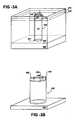
- FIG. 1Ais a cross sectional view of a memory device of the present invention comprising multi-region conductive sidewall spacers;
- FIG. 1Bis a three-dimensional view of a portion of the memory device shown in FIG. 1A;
- FIG. 1Cis a cross sectional view of a memory device of the present invention having angled multi-region conductive sidewall spacers
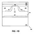
- FIG. 1Dis a cross sectional view along the channel width of a memory element having a narrowed edge adjacent to the memory material
- FIG. 1Eis the narrowed conductive sidewall spacer of FIG. 1D showing placement of a more resistive region R 2 adjacent to the memory material and a less resistive region R 1 remote to the memory material;
- FIG. 1Fshows a memory device having an intermediate layer disposed between the memory material and the conductive sidewall spacers
- FIG. 1Gshows a memory device wherein the conductive sidewall spacers have an additional region R 3 adjacent to the memory material
- FIGS. 2 A′- 2 D′show an alternate process for making a memory device having multi-region conductive spacers as electrical contacts
- FIG. 3Ais a three-dimensional view of a memory device of the present invention having a multi-region cylindrically shaped conductive sidewall spacer as an electrical contact;
- FIG. 3Bis a three-dimensional view of cylindrically shaped conductive sidewall spacer with columnar protrusions
- FIG. 4Ais a conductive liner formed in a trench
- FIG. 4Bis a conductive liner formed in a rectangular via
- FIG. 4Cis a conductive liner formed in a circular via
- FIG. 5Ais a three-dimensional view of a memory device having a multi-region conductive liner as an electrical contact
- FIG. 5Bis a cross-sectional view of the memory device of FIG. 5A;
- FIG. 5Cis a three-demensional view of a cylindrically shaped conductive liner with columnar protrusions
- FIGS. 6A-6Gis a process for making a memory device of the present invention having a multi-region conductive liner as an electrical contact;
- FIG. 7Ais a three-dimensional view of a memory element of the present invention having a horizontally disposed contact layer edgewise adjacent to a volume of memory material;
- FIG. 7Bis a cross-sectional view of the memory element from FIG. 7A.
- the present inventionis directed to electrically programmable memory elements and, in particular, to programmable resistance memory elements.
- the memory elementpreferably comprises a volume of memory material which is programmable between at least a first resistance state and a second resistance state in response to an electrical signal.
- the memory elementfurther comprises a means of delivering the electrical signal to the volume of memory material.
- the means of delivering the electrical signalcomprises one or more electrical contacts which are in electrical communication with the volume of memory material.
- At least one of the electrical contactsis a conductive sidewall spacer.
- the conductive sidewall spaceris in electrical communication with the volume of memory material.
- substantially all of said electrical communicationis through at least a portion of an edge of the conductive sidewall spacer. That is, substantially all of the electrical communication is through an edge or a portion of an edge of the conductive sidewall spacer.
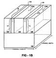
- FIG. 1Ais an example of this first embodiment. Shown is a cross-sectional view of a memory device 100 of the present invention formed on a semiconductor substrate 102 .
- the “channel length” of the memory device 100is parallel to the plane of the illustration.
- the “channel width” of the memory device(not shown in FIG. 1A) is perpendicular to the plane of the illustration.
- the memory device 100comprises two independent single-cell memory elements.
- the first memory elementcomprises a first contact 130 A, a layer of memory material 250 and a second contact 270 .
- the second memory elementcomprises a first contact 130 B, a layer of memory material 250 and a second contact 270 .
- the volume of memory materialis a substantially horizontally disposed layer of memory material 250 .
- the layer of memory material 250 and the second contact 270are shared by the first and second memory elements.
- each memory elementhas a unique corresponding volume (or layer) of memory material and a unique corresponding second contact.
- the dielectric region 140electrically isolates the electrical contact 130 A from the electrical contact 130 B.
- An upper dielectric region 180is deposited on top of the memory device 100 .
- the upper dielectric layer 180may comprise boron-phosphate silica glass (BPSG).
- Each of the electrical contacts 130 A and 130 Bis in the form of a conductive sidewall spacer.
- reference to the “conductive sidewall spacer 130 A,B”refers to either conductive spacer 130 A or conductive spacer 130 B.
- Reference to the “conductive sidewall spacers 130 A,B”refers to both conductive spacers 130 A and 130 B of device 100 .
- each conductive sidewall spacer 130 A,Bis “single-layered”. That is, each conductive spacer 130 A,B is a single, substantially vertically disposed, sidewall layer. Each sidewall layer may be formed by the substantial conformal deposition of a suitable contact material onto a sidewall surface 128 S. (In FIG. 1, sidewall surfaces 128 S and bottom surface 106 form a trench extending perpendicular to the plane of the illustration of FIG. 1 A).
- a “single-layered” conductive spaceris distinguishable from a “multi-layered” conductive spacer where one or more additional sidewall layers are substantially conformally deposited onto the surface of an existing sidewall layer. (Of course, contacts in the form of multi-layered conductive spacers are also possible).
- the layer of memory material 250is deposited onto the conductive spacer 130 A,B so that only the top end 132 of the conductive spacer 130 A,B is adjacent to the memory material 250 . The remainder of the conductive spacer is remote to the memory material. Hence, substantially all electrical communication between the conductive spacer 130 A,B and the memory material 250 is through the top end 132 of the conductive spacer.
- the terminology “above” and “below” as well as the terminology “top” and “bottom”are defined in terms of relative distances from the substrate. The terminology is independent of the orientation of the substrate.
- the top end of the conductive spacer 130 A,Bis an edge of the conductive spacer (i.e., the “top edge”).
- An example of an edge of a layeris a surface substantially parallel to the thickness dimension of the layer (where the thickness is preferably the layer's smallest dimension).
- the conductive sidewall spacer 130 A,Bis a substantially vertically disposed sidewall layer.
- the thickness “t” of the conductive spacer 130 A,Bis the dimension of the sidewall layer substantially parallel to the channel length
- the top edge 132is a surface substantially parallel to the substrate 102 .
- FIG. 1Bis a three-dimensional view of the conductive spacer 130 A,B showing its thickness “t”, width “w” and a height “h”.
- the thickness “t” of the conductive sidewall spacer 130 A,Bis the dimension of the spacer along the channel length (parallel to plane of the illustration).
- the width “w”is the dimension of the conductive spacer along the channel width (perpendicular to the plane of the illustration of FIG. 1A)
- the height “h”is the distance above the substrate 102 .
- each conductive spacer 130 A,Bis adjacent to the memory material 250 while the remainder of each conductive spacer is remote to the memory material. Hence, substantially all electrical communication between the conductive spacer 130 A,B and the memory material 250 is through at least a portion of the top edge 132 . That is, substantially all electrical communication is through all or a portion of the top edge 132 . It is noted that the top edge 132 need not be in actually contact with the memory material.
- the memory material 250is adjacent to the entire top edge 132 of both conductive spacers 130 A,B.
- the conductive spacers 130 A,Bare sidewall layers which are substantially vertically disposed and thus substantially perpendicular to the layer of memory material 250 and to the substrate. It is, of course, also possible that the conductive spacers 130 A,B be “tilted” so that they are not substantially perpendicular to the memory material. As shown in FIG. 1C, the sidewall layers 130 A,B may be formed on “angled” sidewall surfaces 128 s (for example, the sidewall spacers 130 A,B could be formed in a V-shaped trench). This type of structure is also within the spirit and scope of the present invention. The surfaces 132 shown in FIG. 1C (substantially parallel to the substrate) are also considered “edges” of the conductive sidewall spacers 130 A,B of FIG. 1 C.
- the layers 130 A,Bform an angle of incidence “THETA” with the layer of memory material 250 .
- THETAis greater than 30° and less than 150°. More preferably, THETA is greater than 45° and less than 135°. Most preferably, THETA is greater than 60° and less than 120°.
- each conductive spacer 130 A,Bis the surfaces defined by the thickness “t” and the height “h”.
- the conductive spaceris “edgewise adjacent” to the memory material. That is, only an edge or a portion of an edge of the conductive spacer 130 A,B is adjacent to the memory material. Substantially all of the remainder of the conductive spacer is remote to the memory material.
- substantially all of the electrical communication between the conductive sidewall spaceris through an edge of the conductive spacer or a portion of an edge. That is, it is preferable that substantially all electrical communication is through at least a portion of an edge (i.e., an “edge portion”) of the conductive sidewall spacer.
- the terminology “area of contact”is the portion of the surface of an electrical contact through which the electrical contact electrically communicates with the memory material. As noted, it is preferable that substantially all electrical communication between the memory material 250 and a conductive sidewall spacer 130 A,B occurs through all or a portion of an edge of the conductive spacer (for example, through all or a portion of the top edge 132 ). Hence, the area of contact between the conductive spacer 130 A,B and the memory material 250 is an edge of the conductive sidewall spacer or a portion of an edge of the conductive sidewall spacer. That is, the area of contact between the conductive spacer and the memory material is an “edge portion” of the conductive sidewall spacer.
- the conductive spacerneed not actually physically contact the memory material. It is sufficient that the conductive spacer is in electrical communication with the memory material.
- the area of contact, being only an edge portion (i.e., an edge or a portion of an edge) of the conductive spacer,is thus very small and is proportional to the thickness of the conductive spacer.
- the conductive sidewall spacersare edgewise adjacent to the memory material, this does not have to be the case. It is conceivable that other embodiments are also possible.
- the area of contact between the conductive spacer and the memory materialmay be all or a portion of a side face of the conductive spacer (that is the surface defined by the height “h” and width “w” as shown in FIG. 1 B).
- each of the conductive sidewall spacers 130 A,Bis multi-regioned.
- each single sidewall layer 130 A,Bcomprises at least a first region R 1 having a first resistivity and a second region R 2 having a second resistivity.
- the resistivity of the second region R 2is greater than the resistivity of the first region R 1 .
- the first and second regionsmay be positioned anywhere within the conductive sidewall spacer. There are many different ways of positioning the regions within the conductive sidewall spacer. For example, the more resistive second region R 2 may be positioned adjacent to the memory material. In addition the less resistive first region may be positioned remote to the memory material.
- the more resistive second regionmay be adjacent to the area of contact between the memory material and the conductive spacer while the less resistive first region may be remote to the area of contact.
- Area of contactwas defined above as the surface portion of the conductive sidewall spacer through which the electrical communication with the memory material occurs).
- the more resistive second regionmay be adjacent to an edge of the conductive spacer (for example, the top edge) and the less resistive first region may be remote to this edge.
- the area of contact between the memory material and the conductive spacermay be an edge portion of the conductive spacer.
- the more resistive region R 2may be positioned adjacent to the edge portion defining the area of contact and the less resistive region R 1 may be positioned remote to the edge portion defining the area of contact.
- the conductive spacermay be “edgewise adjacent” to the memory material. That is, only an edge or a portion of an edge—i.e., an edge portion of the conductive spacer 130 A,B, is adjacent to the memory material while substantially all of the remainder of the conductive spacer is remote to the memory material. Hence, the more resistive region R 2 may be positioned adjacent to the edge portion that is adjacent to the memory material while the less resistive region R 1 is positioned remote to this edge portion.
- Certain embodiments of the memory elementmay satisfy more than one of the configurations discussed above. Other configurations are also; possible. As discussed above, the present invention is not limited to any specific configuration or configurations. Furthermore, while the possible ways of positioning the first and second regions R 1 , R 2 was discussed in regards to a conductive sidewall spacer, the discussion is applicable to all embodiments of the present invention.
- the more resistive second region R 2is a portion of the conductive sidewall layer.
- this portion of the sidewall layer(that is, this “layer portion”) includes at least a portion of an edge of the sidewall layer (that is, the more resistive sidewall layer portion R 2 preferably includes an “edge portion” of the sidewall layer).
- the more resistive second region R 2is a “top portion” of the conductive spacer that includes the top edge 132 (and remote to substrate 102 ). That is, it extends from the top edge 132 downwardly (i.e., toward the substrate 102 ) into the interior of the conductive spacer for some distance “h 2 ” (the “height” of the more resistive section region R 2 ).
- the distance “h 2 ”is not fixed. It may be very small, for example, between about 10 to about 20 Angstroms. In this case, the more resistive top portion is essentially the surface defined by all or a portion of the top edge. Alternately, the distance “h 2 ” may extend further below the top edge 132 and into the interior of the conductive spacer. For example, the distance “h 2 ” may be about 500 Angstroms to about 600 Angstroms.
- the height “h 2 ” of the regions R 2are preferably less than about 1000 Angstroms, more preferably less than about 800 Angstroms, and most preferably less than about 600 Angstroms.
- the less resistive region R 1is remote to the top edge 132 . In the example shown, it extends from the bottom of the first region R 2 to the substrate 102 .
- the height “h 1 ” of the first region R 1is indicated in FIG. 1 A.
- the height of regions R 1is preferably less than about 10,000 Angstroms, more preferably, less than about 7,000 Angstroms, most preferably less than about 5,000 Angstroms.
- region R 1 , region R 2 and the memory materialare is electrical series. It is further noted that in the embodiment shown in FIG. 1A, conductive sidewall spacer 130 A,B comprises only two regions R 1 and R 2 . However, in other embodiments, one or both of the conductive spacers 130 A,B may comprise more than two regions of material.
- Examples of materials which may be used for the more resistive second region R 2include n-type doped polysilicon, p-type doped polysilicon, n-type doped silicon carbon compounds and/or alloys, p-type doped silicon carbon compounds and/or alloys, titanium carbon-nitride, titanium aluminum nitride, titanium silicon-nitride, carbon, and forms of titanium nitride.
- Examples of materials which may be used for the less resistive first region R 1include n-type doped polysilicon, p-type doped polysilicon, n-type doped silicon carbide, p-type doped silicon carbide, titanium-tungsten, tungsten silicide, tungsten, molydenum, and titanium nitride.
- each of the conductive sidewall spacers 130 A,Bdelivers electrical current to the memory material.
- the electrical currentpasses through the conductive sidewall spacers and through the memory material, at least a portion of the electric potential energy of the electrons is transferred to the surrounding material as heat. That is, the electrical energy is converted to heat energy via Joule heating.
- the amount of electrical energy converted to heat energyincreases with the resistivity of the material as well as with the current density passing through the material.
- the conductive sidewall spacers of the present inventionmay be formed having a more resistive material adjacent to the memory material and a less resistive material remote to the memory material.
- the multi-region sidewall spacermay be referred to as a “matchstick” contact. It has a relatively “cooler” bottom portion R 1 and relatively “hotter” top portion R 2 .
- dissipating power in the electrical contact from Joule heating adjacent to the memory materialmay at least partially assist (or may even dominate) the programming of the memory material. It is also believed that dissipating power in the electrical contact remote to the memory material may actually waste power and increase the total energy needed to program the memory material. Hence, providing an electrical contact structure having a relatively high power dissipation adjacent to the memory material and a relatively low power dissipation remote to the memory material may thus decrease the total power and energy needed to program the memory device.
- the conductive sidewall spacermay be edgewise adjacent to the memory material and the area of contact between the memory material and the conductive sidewall spacer may be an edge or a portion of an edge of the conductive spacer. This is a very small area of contact. While not wishing to be bound by theory it is believed that reducing the size of the area of contact reduces the volume of the memory material which is programmed, thereby reducing the total current needed to program the memory device.
- the use of a specially designed “multi-region” conductive sidewall spacer as an electrical contact as well as the unique positioning of the conductive spacer relative to the memory materialprovides for more efficient heating of the memory material as well as for more efficient use of the total energy supplied to the memory element. Hence, less total energy may be needed to affect a state change in the memory material (that is, less energy may be needed to program the device).
- the multi-region conductive spacerprovides a way to increase the flow of the heat energy into the memory material.
- a layer of insulation materialmay optionally be placed so that it at least partially surrounds the memory material.
- a layer of insulation materialmay be disposed in between the memory material 250 and a portion of the second contact 270 to provide a “thermal blanket” for the memory material and serving to keep heat energy within the memory material layer 250 .
- each conductive sidewall spacer 130 A,Bhas a substantially uniform width “w”.
- the conductive spacermay be formed so that the width narrows or tapers adjacent to the memory material (i.e. remote to the substrate).
- This embodimentreferred to as a “narrowed” or “rapier” conductive spacer, is shown in FIG. 1 D.
- FIG. 1Dis a two-dimensional view of a memory device 100 ′ using a “narrowed” conductive sidewall spacer with a “rapier” design. The plane of the illustration is parallel to the channel width of the memory device 100 ′.
- the conductive spacerhas been appropriately etched so that its width decreases adjacent to the memory material.
- the conductive spacerhas been appropriately etched to form a columnar portion 135 which protrudes upwardly toward the material 250 .
- the height of the columnar protrusion as well as the extent of any taperingmay be controlled to adjust the width w 2 adjacent to the memory material.
- Dielectric material 145is positioned between the remainder of the conductive spacer 130 ′ and the memory material.
- the width w 2 of the conductive spacer adjacent to the memory materialis less than the width “w 1 ” of the conductive spacer adjacent to the substrate.
- the surface portion of the conductive sidewall spacer 130 ′ through which the conductive spacer 130 ′ electrically communicates with the memory material 250is referred to as the “area of contact” between the conductive spacer 130 ′ and the memory material.
- the area of contactis the surface portion defined by the width “w 2 ” and the thickness “t” of the conductive spacer 130 ′ (the thickness being perpendicular to the plane of the illustration). Decreasing the width “w 2 ” of the conductive spacer adjacent to the memory material and/or decreasing the thickness “t” of the conductive spacer decreases the area of contact with the memory material.
- the area of contact defined by the width “w 2 ” and thickness “t”may be viewed as the “top edge” of the narrowed conductive spacer. Alternately, the area of contact defined by the width “w 2 ” and thickness “t” may be viewed as a portion of the edge defined by segments “s 1 +w 2 +S 2 ” and thickness “t”. In either case, the area of contact between the conductive spacer 130 ′ and the memory material 250 (that is, the surface portion of the conductive spacer 130 ′ through which substantially all electrical communication occurs) is all or a portion of an edge of the narrowed conductive sidewall spacer 130 ′.
- the narrowed conductive sidewall spacermay also include at least a first region R 1 with a first resistivity and a second region R 2 with a second resistivity greater than the first resistivity.
- FIG. 1 EAn example of a specific configuration is shown in FIG. 1 E. Referring to FIG. 1E, it is seen that the more resistive region R 2 is adjacent to the area.of contact (i.e., the surface defined by width “w 2 ” and thickness “t”) and the less resistive region R 1 is remote to the area of contact. (It is, of course, also the case that the more resistive region R 2 is adjacent to the memory material while the less resistive region R 1 is remote to the memory material).
- the narrowed conductive sidewall spacer 130 ′may be made by forming an oxide spacer over the conductive spacer 130 A,B shown in FIGS. 1A and 1B. Specifically, the oxide spacer is positioned along the width of the conductive spacer where it is desired to position the protruding column 135 .
- the oxide spaceris a mask for either an anisotropic or isotropic etch. That is, the exposed sections of the conductive spacer will be etched away while the section underlying the mask be protected from the etch so as to form the column 135 .
- FIGS. 2A-2HAn embodiment of a method for fabricating the memory device 100 from FIG. 1A is shown in FIGS. 2A-2H.
- a substrate 102is provided and a dielectric layer 128 is deposited on top of the substrate 102 to form the structure 200 A shown in FIG. 2 A.
- the dielectric layer 128may be a dielectric material such as silicon dioxide SiO 2 which may be deposited by means such as chemical vapor deposition (CVD).
- the dielectric layer 128is then appropriately masked and etched to form the structure 200 B having a trench 170 which runs perpendicular to the plane of the illustration.
- the trench 170has sidewall surfaces 128 S (corresponding to the sidewall surfaces of the dielectric regions 128 ) and bottom surface 106 .
- a layer 133 of a contact materialis deposited onto the structure 200 B to form the structure 200 C shown in FIG. 2 C.
- the depositionis a conformal deposition.
- the layer 133is deposited onto the top surfaces 128 T of the dielectric regions 128 , onto the sidewall surfaces 128 S of the dielectric regions 128 , and onto the bottom surface 106 of the trench 170 .
- portions of the layer 133are deposited along the two sidewall surfaces 128 S of the trench 170 .
- These portions of the layer 133are sidewall layer portions 133 S of the layer 133 .
- the conformal deposition of layer 133may be done using chemical vapor deposition techniques.
- the material of layer 133will form the first region R 1 of the conductive sidewall spacers 130 A,B that are shown in FIG. 1 A.
- the material used for layer 133is preferably a conductive material having the appropriate resistivity.
- Materials which may be used for layer 133are those which are suitable for the first region R 1 . As noted above, these materials include n-type doped polysilicon, p-type doped polysilicon, n-type doped silicon carbide, p-type doped silicon carbide, titanium-tungsten, tungsten silicide, tungsten, molydenum, and titanium nitride.
- the n-type polysiliconmay be formed “in situ” by depositing undoped polysilicon in the trench 170 using a CVD process in the presence of phosphene. Alternately, the n-type polysilicon may be formed by first depositing undoped polysilicon and then doping the polysilicon with phosphorous or arsenic. P-type doped polysilicon may be formed by first depositing undoped polysilicon and then doping the polysilicon with boron.
- the layer 133is conformally deposited it is then anisotropically etched.
- the anisotropic etchremoves those sections of the layer 133 which are substantially horizontally disposed and leaves those sections which are substantially vertically disposed. Specifically, the anisotropic etch removes the substantially horizontally disposed sections of the layer 133 that were deposited on top surfaces 128 T of the regions 128 . It also removes the substantially horizontally disposed section of the layer 133 deposited onto the bottom surface 106 of trench 170 .
- the anisotropic etchleaves those sections of the layer 133 conformally deposited along the sidewall surfaces 128 S. Hence, the anisotropic etch leaves the sidewall layer portions 133 S of the layer 133 .
- each of the conductive spacerscomprises only the single sidewall layer 133 S and each sidewall layer 133 S comprises only a single region of material.
- the remaining sidewall layers 133 Sare shown as conductive sidewall spacers 130 A,B.
- the conductive sidewall spacers 130 A,Bwill have a lateral thickness substantially equal to the selected thickness of the layer 133 .
- the layer 133is deposited so that the resulting conductive sidewall spacers 130 A,B have a substantially uniform thickness between about 50 and about 1000 Angstroms, and more preferably between about 100 and about 500 Angstroms. (However, it is possible that the thickness of the deposited sidewall layers is nonuniform).
- the conductive sidewall spacers 130 A,B shown in FIG. 2Dextend continuously along the width of the trench 170 (i.e perpendicular to the plane of the illustration of FIG. 2 D).
- the next step in the processis to mask and etch the conductive sidewall spacers 130 A,B so as to form a plurality of individual conductive sidewall spacers along the width of the memory array. These conductive spacers define individual memory elements along the channel width of the memory array.
- the next step in the processis to fill the trench region 170 with a dielectric material such as silicon dioxide SiO 2 .
- a dielectric materialsuch as silicon dioxide SiO 2 .
- Thismay be done by depositing the dielectric material 140 onto the structure 200 D to form structure 200 E that is shown in FIG. 2 E.
- the dielectric material 140is deposited into the trench 170 as well as onto the top surfaces of the dielectric regions 128 .
- the depositionmay be done using a chemical vapor deposition process.
- the structure 200 Emay then chemically mechanically polished (CMP) or dry etched to form the structure 200 F shown in FIG. 2 F.
- CMPchemically mechanically polished
- the chemical mechanical polishing or dry etchingpreferably planarizes the top surfaces of the conductive spacers to form top edges 132 which are substantially planar (as shown in FIG. 2 F).
- each conductive spacer 130 A,B shown in FIG. 2Fwas formed by the deposition and anisotropic etch of a single layer of material (i.e., layer 133 shown in FIG. 2 C).
- each conductive spacer 130 A,B shown in FIG. 2Fis a single sidewall layer comprising a single region of material. This region of material is denoted as the first region R 1 in FIG. 2 F.
- a second region R 2(as seen in FIG. 1 A), having a greater resistivity than region R 1 , may be formed in each of the conductive spacers 130 A,B in several different ways. The approach used depends, at least in part, on the material of region R 1 .
- One way of forming the second region R 2is to alter a portion of the region R 1 of each conductive spacer 130 A,B so as to increase the resistivity of the R 1 material.
- a “top portion” of the conductive spaceris altered.
- Top portionrefers to a section of the conductive sidewall spacer starting from the top edge 132 (or a portion of the top edge 132 ) and extending downwardly (i.e., toward the substrate) into the interior of the conductive sidewall spacer.
- a top portion of the conductive sidewall spacerincludes all or a portion of the top edge 132 of the conductive spacer.
- any method of increasing the resistivity of the materialis within the spirit and scope of this invention.
- the resistance of the materialmay be increased using ion implantation techniques and/or by appropriately doping the material (introducing dopants into the material). This alters the dopant level of the material.
- the second region R 2may be formed by appropriately “counter-doping” a top portion of the region R 1 of each conductive spacer 130 A,B shown in FIG. 2 F.
- a top portion of each region R 1may be counter-doped with boron (by well known ion implantation techniques) to form regions R 2 having a resistivity which is greater than the resistivity of regions R 1 .
- a region R 2may be formed which comprises n-polysilicon. If the n-type polysilicon of region R 1 is more heavily counter-doped with boron, then a region R 2 may be formed which comprises p-polysilicon.
- each region R 1may be counter-doped with phosphorous to form regions R 2 which also have a resistivity greater than the resistivity of regions R 1 . If the p-type polysilicon of region R 1 is lightly counter-doped with phosphorous, then a region R 2 may be formed which comprises p-polysilicon. If the p-type polysilicon of region R 1 is more heavily counter-doped with phosphorous, than a region R 2 may be formed which comprises n-polysilicon.
- a top portion of the first region R 1may be counter-doped to form a second region R 2 which has a higher resistivity than the first region R 1 .
- a top portion of the region R 1may be sufficiently counter-doped with boron to form a second region R 2 comprising n-polysilicon.
- a top portion of the region R 1may be sufficiently counter-doped with boron to form a second region R 2 comprising p-polysilicon. In either case, the second region R 2 is doped differently from the first region R 1 .
- the multi-region conductive sidewall spacers 130 A,B comprising a first region of material R 1 and a second region of material R 2is shown in FIG. 2 G.
- the more resistive regions R 2start at the top edges 132 .
- the height “h 2 ” of the regions R 2are preferably less than about 1000 Angstroms, more preferably less than about 800 Angstroms, and most preferably less than about 600 Angstroms.
- the height of regions R 1is preferably less than about 10,000 Angstroms, more preferably, less than about 7,000 Angstroms, most preferably less than about 5,000 Angstroms. Of course, the heights of regions R 1 and R 2 may vary.
- the structure 200 His formed by depositing a layer of memory material 250 on top of the structure shown in FIG. 2G.
- a layer of contact material 270is then deposited on top of the memory layer 250 to form a second contact. While not shown in FIG. 2H, it is possible that the second contact 270 may also be formed to include at least a first region having a first resistivity and a second region having a second resistivity greater than the first resistivity.
- the deposited memory layer 250is in contact with only each of the top edges 132 or a portion of each of the top edges 132 of the conductive spacers 130 A,B. Substantially all electrical communication between each conductive spacer 132 A,B and the memory material is through the edge 132 or a portion of the edge 132 of the respective conductive spacer.
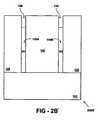
- FIGS. 2 A′- 2 D′show conductive sidewall spacers 130 A,B comprising a single sidewall layer of material R 1 (FIG. 2 A′ is the same as FIG. 2 F).
- the structure 200 A′may be masked and selectively etched to remove a portion (in particular, a top portion) of the conductive sidewall spacers 130 A,B so as to create recesses in a top portion of material R 1 of each of the conductive spacers 130 A,B.
- the recesses 150are shown in structure 200 B′.
- the recesses 150are filled by depositing a layer of material 160 on top of structure 200 B′ to form the structure 200 C′ shown in FIG. 2 C′. As shown in FIG. 2 C′, the layer 160 fills the recesses 150 and also lies on top of the dielectric regions 128 , 140 .
- the structure 200 C′may then be chemically mechanically polished (CMP) or dry etched to form the substantially planar top edges 132 as shown in structure 200 D′ of FIG. 2 D′.
- the structure 200 D′includes conductive sidewall spacers 130 A,B where each of the conductive spacers includes two regions of material—the first region R 1 and the second region R 2 .
- the regions R 2consist of the material of layer 160 shown in FIG. 2 C′. It is noted that the structure shown in FIG. 2 D′ is the same as the structure shown in FIG. 2 G.
- the second regions R 2 shown in FIG. 2 D′may be formed of a material which, without any further modification, has the appropriate resistivity.
- the material chosen for the second region R 2has a resistivity that is greater than the resistivity of the R 1 material removed by the etching process to create the recesses 150 (shown in FIG. 2 B′).
- appropriate materialsinclude n-doped polysilicon, p-doped polysilicon, n-doped silicon carbon compounds and/or alloys, p-doped silicon carbon compounds and/or alloys, titanium carbon-nitride, titanium aluminum nitride, titanium silicon-nitride, carbon, and forms of titanium nitride.
- the second regions R 2may initially be formed from a material that still needs to be altered to change its resistivity.
- the second region R 2may be formed from undoped polysilicon (that is, the layer 160 shown in FIG. 2 C′ may be deposited as an undoped polysilicon).
- the undoped polysilicon of the second regions R 2may then be doped with boron to form a p-polysilicon region.
- the undoped polysilicon of the second regions R 2may be doped with a material such as phosphorous or arsenic to form an n-polysilicon region.
- an electrical contact for each of the single-cell memory elements in the deviceis a conductive sidewall spacer.
- the conductive sidewall spacer 130 A,Bis a single sidewall layer formed along the sidewall surface of a trench by depositing a layer of conductive material into the trench and then anisotropically etching the layer to remove the horizontally disposed surfaces.
- the shape of the conductive spacer shown in FIGS. 1A and 1Bare in the form of substantially planar sidewall layers.
- Alternate forms of electrical contactsmay be formed from sidewall layers that are made by the conformal deposition of material onto the other types of sidewall surfaces (that is, sidewall surfaces other that the sidewall surfaces of a trench).
- a layer of conductive materialmay be substantially conformally deposited onto the surfaces of a via (a hole), mesa or pillar.
- the via, mesa or pillarmay be round, square, rectangular or irregularly shaped.
- Anisotropically etching the conformally deposited conductive layerremoves the horizontally disposed portions of the deposited layer and leaves only one or more vertically disposed portions. The remaining one or more vertically disposed portions are sidewall layers in the form of conductive sidewall spacers.
- the sidewall spacer formed, for example, by the conformal deposition of a conductive material into a cylindrical via (followed by an anisotropic etch)will be in the form of a cylindrical surface (with an axis substantially perpendicular to the substrate) having two open ends.
- Changing the shape of the via (or pillar or mesa)will change the shape of the sidewall spacer. That is, the lateral cross section of the conductive sidewall spacer (i.e. the cross section parallel to the substrate) corresponds to the shape of the via, mesa or pillar. It may be an annulus. Alternately, it may be rectangular or irregularly shaped.
- FIG. 3Ashows a three-dimensional view of a cylindrical, multi-region conductive sidewall spacer 330 formed in a circular via (and thus having a horizontal cross-section in the shape of an annulus).
- the cylindrical conductive spacer 330is “single-layered”. That is, it comprises a single, cylindrically shaped sidewall layer.
- the thickness “t” of this cylindrically shaped sidewall layeris the distance between the inner and outer cylindrical surfaces as shown in FIG. 3 A.
- the cylindrical sidewall layerhas two open ends or “rims” forming the top edge 332 and the bottom edge 331 .
- the top and bottom edges 332 and 331 of the cylindrically shaped conductive sidewall layer 330are annular surfaces formed by intersecting the conductive layer 330 with a planes substantially parallel to the substrate.
- the layer of memory material 250is adjacent only to the top end of the cylindrical sidewall spacer 330 .
- the memory material 250is adjacent only to the top edge 332 .
- the layer 250 of memory materialis deposited on top of the conductive spacer 330 and the second contact layer 270 is deposited on top of the memory material 250 .
- the layer 250 of memory material(which is preferably substantially horizontally disposed) is adjacent only to the top edge 332 or portion of the top edge 332 of the conductive sidewall spacer 330 is adjacent to the memory material 250 . All electrical communication between the conductive spacer 330 and the memory material 250 is through the top edge 332 or a portion of the top edge 332 .
- area of contact between the conductive spacer 330 and the memory material 250is the edge 332 or a portion of the edge 332 . (That is, all or a portion of the annular surface 332 ).
- the conductive spacer 330comprises at least a first region R 1 having a first resistivity and a second region R 2 having a second resistivity.
- the resistivity of the second region R 2is greater than the resistivity of the first region R 1 .
- the more resistive second region R 2is adjacent to the memory material while the first region R 1 is remote to the memory material.
- the more resistive second region R 2is a “top portion” of the conductive spacer adjacent to the top edge 332 (and remote to substrate 102 ). That is, it extends from the top edge 332 downwardly (i.e., toward the substrate 102 ) into the interior of the cylindrical conductive spacer for some distance “h 2 ” (the “height” of the more resistive section region R 2 ).
- the regions R 1 and R 2 of the cylindrically shaped conductive spacermay be formed by methods similar to those used to form the regions R 1 and R 2 of the “planer” conductive spacer 130 A,B shown in FIG. 1 A.
- a more resistive second region R 2may be form by the appropriate ion-implantation techniques. Such ion implantation techniques may be used to appropriately counter-dope the material R 1 to form the more resistive material R 2 . Alternately, the material R 1 may first be etched and refilled with a more resistive material R 2 .
- all of the methods and materials described aboveare applicable to this embodiment.
- FIG. 3Bshows an alternate embodiment of a cylindrical conductive sidewall spacer 330 ′.
- This cylindrical conductive sidewall spacerincludes at least one columnar portion which protrudes toward the memory material (not shown in this diagram).
- the columnar portions 350each have a thickness which is substantially the same as the thickness of the remainder of the conductive spacer.
- FIG. 3Bshows the cylindrical conductive sidewall spacer 330 ′ disposed on top of a substrate 102 .
- Such columnar protrusionsmay be used with conductive sidewall spacers of all different shapes.
- the columnar protrusionsmay be formed with the use of oxide spacers.
- substantially all electrical communication between the conductive spacer 330 ′ and the memory materialis through one or more of the tips 352 of the columnar protrusions 350 .
- the contact 330 ′ and memory materialmay be positioned so that only the tip(s) 352 of one or more of the columnar protrusions 350 is/are adjacent to the memory material while substantially all of the remaining portion of the contact is remote to the memory material.
- the columnar protrusions 350may also include at least a first region R 1 with a first resistivity and a second region R 2 with a second resistivity greater than the first resistivity. The more resistive region is preferably adjacent to the memory material while the less resistive region is preferably remote to memory material. In the examples of the memory device shown in FIGS.
- the conductive sidewall spacer 130 A,B (or 330 )is adjacent to the memory material such that there are no “intermediate” layers disposed between the memory material and the conductive sidewall spacer 130 A,B (or 330 ).
- one or more intermediate layersexit between the conductive sidewall spacer and the memory material.
- FIG. 1Fshows an intermediate layer 280 is disposed between the memory layer 250 and the conductive sidewall spacer 130 A,B.
- substantially all electrical communication between the memory material 250 and the conductive sidewall spacer 130 A,Bis through the top edge 132 or a portion of top edge 132 of the conductive spacer 130 A,B even though the layer 280 is disposed between the memory material 250 and the conductive spacer 130 A,B.
- FIG. 1Fwhere an intermediate layer 280 is disposed between the memory layer 250 and the conductive sidewall spacer 130 A,B.
- the more resistive second region R 2is adjacent to the area of contact (which is top edge 132 ) while the less resistive first region R 1 is remote to the area of contact (which is top edge 132 ). Also, it is seen that the more resistive second region R 2 is positioned closer to the memory material 250 than the less resistive first region R 1 . That is, the second region R 2 is “proximate to” the memory material while the first region R 1 is “distant from” the memory material.
- the conductive sidewall spacers(such conductive spacers 130 A,B in FIG. 1A or conductive spacer 330 in FIG. 3) comprise one or more regions of material in addition to the more resistive second region R 2 and the less resistive first region R 1 .
- the conductive sidewall spacers 130 A,Beach comprise a third region R 3 disposed between the memory material 250 and the second region R 2 . It is noted that in this embodiment, it is still the case that substantially all electrical communication between the memory material and the conductive sidewall spacer 130 A,B is through the top edge 132 or a portion of the top edge 132 .
- the first and second regions R 1 and R 2are positioned so that the region R 2 is closer to the top edge 132 than region R 1 . (That is, region R 2 is “proximate to” the top edge 132 while the region R 1 is “distant from” to the top edge 132 ). Hence, region R 2 is also closer to the area of contact between the conductive spacer and the memory material while the region R 1 is further from the area of contact. (That is, region R 2 is “proximate to” the area of contact while region R 1 is “distant from” from the area of contact). Furthermore, it is also true that region R 2 is closer to the memory material than region R 1 . (That is, region R 2 is “proximate to” the memory material 250 while region R 1 is “distant from” from the memory material).
- an electrical contact for a programmable resistance memory elementmay also be formed as a “conductive liner”.
- the conductive lineris preferably a single layer of conductive material covering the sidewall surfaces as well as the bottom surface of a trench, via, or the like. Examples of conductive liners are shown in FIGS. 4A-C.
- FIG. 4Athe conductive liner 430 A is formed in a trench.
- FIG. 4Bis an example of a conductive liner 430 B formed in a rectangular via hole.
- FIG. 4Cis an example of a conductive liner 430 C formed in a circular via hole. Of course, other shapes are also possible. As shown in the FIGS.
- each conductive linerhas one or more sidewall layer portions as well as a bottom layer portion.
- the top end of the conductive linersis an open end having a top edge 432 .
- the “top edge” 432 of each conductive lineris the surface formed by intersecting the respective conductive liner with a plane substantially parallel with the substrate 102 ). It is noted that the U-shaped conductive liner shown in FIG. 4A has a “dual” top edge 432 .
- the sidewall layer portionsare substantially vertically disposed. However, this does not have to be the case.
- the sidewall layer portionsmay be tilted. This would be the case if the conductive liners were formed in either a trench or via having angled sidewall surfaces.
- the conductive lineris preferably edgewise adjacent to the memory material. That is, only an edge or a portion of an edge of the conductive liner is adjacent to the memory material. Substantially all of the remainder of the conductive liner is remote to the memory material. Preferably, substantially all electrical communication between the conductive liner and the memory material is through an edge or a portion of an edge of the conductive liner (that is, through an “edge portion” of the conductive liner.
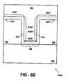
- FIGS. 5A and 5Bdepict an embodiment of the memory element of the present invention where one of the electrical contacts is a conductive liner 530 formed in a circular via hole.
- FIG. 5Ais a three-dimensional view of the memory element.
- FIG. 5Bis a cross-sectional view formed by intersecting a vertical plane through the memory element.
- the conductive liner 530is a cylindrical shell having an open top end (remote to and facing away from the substrate 102 ) and a closed bottom end (proximate to the substrate).
- the open top endhas an annular-shaped top edge 532 .
- the conductive liner 530is a cylindrically shaped sidewall layer portion 530 S and a bottom layer portion 530 B.
- the conductive liner 530is in the shape of a cylindrically shaped cup. As shown in FIG. 5B, the sidewall layer portion 530 S forms the side of the cup while the bottom layer portion 530 B forms the bottom of the cup.
- the top edge 532may be referred to as the “rim” of the cup.
- the conductive linermay have other cup shapes such as a paraboloid, hemisphere, cone, and frustum.
- the layer 250 of memory materialis preferably a planar, substantially horizontally disposed layer positioned adjacent to the open end of the conductive liner 530 .
- the memory materialis adjacent only to the top edge 532 (i.e., the rim) of the conductive liner 530 or a portion of the top edge 532 of the conductive liner.
- the remainder of the conductive liner 530is remote to the memory material.
- substantially all electrical communication between the conductive liner 530 and the memory materialoccurs through the edge 532 or a portion of the edge 532 .
- the area of contactis defined by all or a portion of the edge 532 (i.e., an edge portion).
- the edge 532is an annulus having a thickness equal to the thickness of the conductive liner 530 .
- the thickness of this annulus, and hence the area of contact between the conductive liner and the memory materialmay be reduced by decreasing the thickness of the conductive liner 530 deposited into the circular via.
- the conductive linersare “multi-regioned” and comprise at least a first region R 1 having a first resistivity and a second region R 2 having a second resistivity which is greater than the resistivity of the first region R 1 .
- the first region R 1 and second region R 2may be positioned anywhere in the conductive liners. Examples of possible ways of positioning the first and second regions were discussed above with regards to conductive sidewall spacers. That entire discussion is applicable to conductive liners.
- the more resistive second region R 2may be positioned adjacent to the memory material while the less resistive first region R 1 may be positioned remote to the memory material.
- the second region R 2is may be positioned adjacent to the area of contact while the region R 1 may be remote to the area of contact. In yet another configuration, the second region R 2 may be positioned adjacent to an edge of the conductive liner while the region R 1 may be positioned remote to this edge.
- the more resistive region R 2is a “top portion” of the conductive liner adjacent to the top edge. 532 and extending for some distance downwardly (toward the substrate) into the interior of the conductive liner. (That is, the more resistive top portion of the conductive liner includes all or a portion of the top edge 532 ).
- one or more intermediate layersbe disposed between the memory material and the conductive liner.
- the conductive linerinclude at least a third region of material in addition to the first and second regions discussed above. The third region may be disposed between the memory material and the more resistive second region.
- FIGS. 6A-6FAn embodiment of a method for fabricating the memory element 500 from FIGS. 5A and 5B is shown in FIGS. 6A-6F.
- a substrate 102is provided and a dielectric layer 128 is deposited on top of the substrate 102 .
- the dielectric layermay be formed from silicon dioxide and may be deposited by a chemical vapor deposition process.
- the dielectric layer 128is then appropriately masked and etched to form a via hole 640 in the dielectric 128 as shown.
- the via holemay be round, square, rectangular or irregularly shaped. (Alternately, the dielectric layer 128 may be masked and etched to form a trench).
- FIG. 6AAn embodiment of a method for fabricating the memory element 500 from FIGS. 5A and 5B is shown in FIGS. 6A-6F.
- a substrate 102is provided and a dielectric layer 128 is deposited on top of the substrate 102 .
- the dielectric layermay be formed from silicon
- the resulting structure 600 Ais a circular via 640 which is formed in the dielectric 128 .
- FIG. 6Bis a vertical cross-sectional view of the structure 600 A shown in FIG. 6 A.
- the sidewall surface 128 S and the bottom surface 106 of the circular via 640is shown in FIG. 6 B.
- a layer 633 of a conductive materialis deposited on top of the structure shown in FIGS. 6A and 6B to form the structure 600 C shown in FIG. 6 C.
- the layer 633 of conductive materialis conformally deposited on top surfaces 128 T of the dielectric region 128 , on the sidewall surface 128 S of the region 128 and the bottom surface 106 of the via hole 640 .
- the layer 633has a top portion 633 T, a sidewall layer portion 633 S, and a bottom layer portion 633 B. It is noted that the layer 633 will form the first region R 1 of the “dual-regioned” conductive liner electrical contact shown in FIGS. 5A and 5B.
- the materials chosen for the layer 633should have the appropriate resistivity.
- n-type doped polysiliconexamples include n-type doped polysilicon, p-type doped polysilicon, n-type doped silicon carbide, p-type doped silicon carbide, titanium tungsten, tungsten silicide, tungsten, molybdenum, and titanium nitride.
- a first region R 1 of n-type polysiliconmay be formed by depositing and doping intrinsic polysilicon. That is, by doping intrinsic polysilicon in situ (i.e., CVD deposition in a phosphene environment).
- n-type polysiliconmay be formed by first depositing intrinsic polysilicon and then doping the polysilicon via ion implantation of phosphorous or arsenic.
- P-type polysiliconmay be formed by first depositing intrinsic polysilicon and then doping the polysilicon via ion implantation of boron. Ion implantation may be performed by an “angle implant” whereby the ion beam comes in at an angle to an axis which is perpendicular to the substrate.
- a layer of dielectric material 140(such as silicon dioxide) may then be deposited on top of the layer 633 so as to fill the via 670 and form the structure 600 D shown in FIG. 6 D.
- the structure 600 Dmay then be chemically mechanically polished (CMP) or dry etched so as to planarize the top surface thereby removing the top surface 633 T portion of the layer 633 and forming a cylindrical, cup-shaped conductive liner.
- CMPchemically mechanically polished
- the conductive liner 630has a sidewall layer portion 630 S along the sidewall 128 S and a bottom layer portion 630 B along the bottom surface 106 .
- the conductive liner 630has a top edge 632 .
- the planarization stepforms a substantially planar top edge 632 .
- the conductive liner 630comprises only a single region of material which is denoted in FIG. 6E as the first region of material R 1 .
- the next stepis to increase the resistivity of a portion of the conductive liner 630 that includes the top edge 632 or a portion of the top edge 632 .
- a second region R 2is formed in a top portion of the conductive liner adjoining the edge 632 .
- the second region R 2 of the conductive linermay be formed by any of the methods which have been described above with regards to forming the multi-region conductive sidewall spacers.
- the second region R 2may be formed by counter doping the n-type polysilicon of the first region R 1 .
- the n-type polysiliconmay be counter doped with boron to form a second region R 2 comprising either n- or p-polysilicon.
- the second regionmay also be implanted with modifier elements in combination with the counter-doping ions or individually.
- a top portion of the first region R 1may be removed (preferably, by being selectively etched) to form a recess. This recess may then be filled with a material which has a resistivity which is greater than the resistivity of the R 1 material.
- the recessmay be filled with a material such as n- or p-polysilicon.
- the recessmay be filled with undoped polysilicon which can then be appropriately doped (preferably with boron, arsenic or phosphorus) to make it more resistive.
- the layer 250 of memory material and the layer 270 of conductive materialmay then be deposited.
- the area of contact between the conductive liner 630 and the memory material 250is the surface portion of the conductive liner through which substantially all electrical communication (between the conductive liner and the memory material) occurs. This may be the entire edge 632 or a portion of the edge 632 . (If the entire edge makes contact with the memory material then the area of contact is in the form of an annular ring). Hence, the memory material 250 is in electrical communication with the conductive liner 630 only through all or a portion of the edge 632 .
- FIG. 5Cshows an alternate embodiment of a cylindrical conductive liner.
- the conductive linerincludes at least one columnar portion 550 which protrudes toward the memory material (the memory material is not shown in this diagram).
- the columnar portions 550each have a thickness which is substantially the same as the thickness of the remainder of the conductive liner 530 ′.
- FIG. 5Cshows the cylindrical conductive liner 530 ′ disposed on top of a substrate 102 .
- the columnar protrusionsmay be formed on all types of conductive liners (for example, they may be formed on the conductive liners shown in FIGS. 4 A- 4 C). Furthermore, they may be formed with the use of oxide spacers.
- substantially all of the electrical communication between the memory material and the conductive liner 530 ′is through a tip 552 of at least one of the columnar protrusions 550 .
- the contact 530 ′ and the memory materialmay be positioned so that only the tip(s) 52 of one or more of the columnar protrusions 550 is/are adjacent to the memory material while substantially all of the remaining portion of the contact is remote to the memory material.
- the columnar protrusions 550may also include at least a first region R 1 with a first resistivity and a second region R 2 with a second resistivity greater than the first resistivity. The more resistive region is preferably adjacent to the memory material while the less resistive region is preferably remote to the memory material.
- an electrically operated memory elementcomprising a volume of memory material and one or more electrical contacts in electrical communication with the memory material.
- substantially, all electrical communication between the memory material and at least one of the contactsis through an edge of a contact or a portion of an edge of a contact.
- the “area of contact” between the contact and the memory materialis an edge or a portion of an edge of the contact (i.e., an edge portion).
- the contactis preferably “edgewise adjacent” to the memory material so that only an edge or a portion of an edge of the contact is adjacent to the memory material while substantially all of the remainder of the contact is remote to the memory material. Examples of edgewise adjacent configurations have been described above.
- the contactmay be in the form of a single layer referred to as a “contact layer”.
- the contact layermay have any shape or conformation. It may be a substantially planar surface. Alternately, it may be a curved surface.
- the layermay be in the shape of a saddle, a cup, a cylinder, a tube, a hemisphere, a cone, a box, etc.
- the contact layermay have any orientation. For example, it may be substantially vertically disposed, substantially horizontally disposed or tilted at some angle.
- the contact layermay be a sidewall layer deposited along a sidewall surface. Any sidewall surface may be used. Examples include the sidewall surface of a trench, via, mesa or pillar. The sidewall surface may also be angled from the substrate and/or angled from the memory material.
- the contact layermay be a substantially vertically disposed layer which is formed in other ways besides with the use of conformal deposition.
- the contact layermay be in the form of a conductive spacer or a conductive liner.
- the contact layermay be cupped shaped.
- the contact layerneed not actually contact the memory material. Also, it is possible that there me one or more intermediate layers between the memory material and the contact layer.
- the contact layeris substantially perpendicular to the volume of memory material. That is, the angle of incidence “THETA” between the memory material and the contact layer is preferably about 90°. Other embodiments are also possible where the contact layer and the memory material are not substantially perpendicular. In one embodiment, the angle of incidence “THETA” between the contact layer and the memory material may be any angle greater than about 15° and less than about 165°. In another embodiment, the angle of incidence “THETA” is preferably between about 30° and 150°, more preferably between about 45° and 135°, and most preferably between about 60° and about 120°.
- positioning the contact layer so that it is substantially perpendicular to the memory materialmay increase the effective amount of heat energy transferred to and remaining within the memory material.
- the area of contact(defined by the edge of the contact layer) is smaller when the contact layer is perpendicular to the memory material.
- the less resistive material R 1may behave as a heat sink, absorbing some of the heat generated by the more resistive portion R 2 (adjacent the memory material). Positioning the contact layer substantially perpendicular to the memory material increases the average distance between the memory material and the less resistive material R 1 of the contact layer. Hence, less of the Joule heat generated in or near the memory material is absorbed back by the contact layer.
- FIG. 7Ashows a three-dimensional view of an embodiment of a memory element 700 of the present invention formed on a substrate 102 .
- the memory element 700comprises the volume of memory material 750 , a first electrical contact in the form of contact layer 730 , and a second electrical contact 770 spacedly disposed from the contact layer 730 .
- the contact layer 730is a substantially horizontally disposed layer having an edge 732 adjacent to the memory material 750 .
- FIG. 7Bis a vertical cross-sectional slice of the same memory device 700 .
- the contact layer 730has a first region R 1 remote to the volume of memory material 750 and a second region R 2 which is adjacent to the memory material 750 .
- the adjacent second region R 2has a higher resistivity than the remote first region R 1 .
- the first contact 730is a contact layer 730 which is substantially horizontally disposed onto the substrate 102 .
- the contact layer 730is edgewise adjacent to the memory material 750 . That is, the contact layer 730 has an edge 732 which is adjacent to the volume of memory material 750 . The remainder of the contact layer 730 is remote to the memory material. Hence, all electrical communication between the contact layer 730 and the memory material 750 is through the edge 732 . Hence, the area of contact between the memory material 750 and the contact layer 730 is the edge 732 of the contact layer 730 . (As shown, in this embodiment the edge is a surface substantially parallel to the thickness of the contact layer). The area of contact between the contact layer 730 and the memory material 750 is proportional to the thickness of the contact layer 730 .
- the edge 732encircles a cross-sectional slice of the volume of memory material 750 .
- “encircles”means that the edge 732 passes completely around a cross-sectional slice of the volume of memory material 750 .
- the memory elementmay be structured so that the edge only partially encircles a cross-sectional slice of the volume of memory material 750 .
- the cross-sectional sliceis substantially parallel to the plane of the substrate 102 , however, other orientations are also possible.
- the second contact 770may be a layer of conductive material and is preferably formed as a thin-film layer. In the embodiment shown in FIGS. 7 A,B, the second contact 770 is a conductive layer deposited on top of the memory material 750 so that the bottom surface of the conductive layer 770 is adjacent to the top surface of memory material 750 .
- one or more intermediate layersmay be disposed between the memory material and the contact layer.
- the contact layermay have one or more additional regions in addition to the first and second regions described above. It is possible that the additional regions be placed anywhere in the contact layer.
- Another embodiment of the present inventionis an electrically operated memory element having a volume of memory material and one or more contacts in electrical communication with the memory material.
- at least one of the contactincludes at least a first region R 1 having a first resistivity and a second region R 2 having a second resisitivity greater than the first resistivity.
- the contactmay have any shape and need not be positioned edgewise adjacent to the memory material (although, as shown in FIG. 1A, it may be).
- FIG. 8shows a memory element 800 having a first contact 830 in electrical communication with memory material 850 .
- Dielectric material 828forms a trench or via structure.
- the first contact 830includes a first region R 1 having a first resistivity and a second region R 2 having a second resistivity greater than the first resistivity.
- the first contact 830is a single layer (that is, it is a single “contact layer”).
- the higher resistivity second regionis adjacent to the memory material while the lower resistivity first region is remote to the memory material. It is noted that in the embodiment shown in FIG. 8, the electrical communication between the first contact 830 is through a portion of a face of the contact layer rather than through an edge of the contact layer.
- the first and second regions R 1 and R 2may be formed from the appropriate contact materials. Examples of appropriate materials have been described above. In one embodiment, the region R 1 and the region R 2 may be differently doped.
- the memory element 800also includes a second contact 870 .
- the second contact 870may also be multi-regioned. That is, it may also include at least a first region having a first resistivity and a second region having a second resistivity greater than the first resistivity.
- the first and second regionsmay be positioned anywhere.
- the more resistive second regionmay be adjacent (either directly or proximately) to the memory material and the less resistive first region may be remote to the memory material. Positioning the more resistive second region adjacent to the memory material and the less resistive first region remote to the memory material provides for more efficient heat transfer from the contact material to the memory material.
- the materials used for the first region R 1 and second region R 2are described above with reference to the conductive spacers and conductive liners.
- the memory elements of the present inventionmay be electrically coupled to isolation/selection devices and to addressing lines in order to form a memory array.
- the isolation/addressing devicespermit each discrete memory cell to be read and written to without interfering with information stored in adjacent or remote memory cells of the array.
- the present inventionis not limited to the use of any specific type of isolation/addressing device.
- isolation/addressing devicesinclude field-effect transistors, bipolar junction transistors, and diodes.
- Examples of field-effect transistorsinclude JFET and MOSFET.
- Examples of MOSFETinclude NMOS transistors and PMOS transistors. Furthermore NMOS and PMOS may even be formed on the same chip for CMOS technologies.
- isolation/addressing devicewhich serves as an isolation/addressing device for that memory element thereby enabling that cell to be read and written without interfering with information stored in other adjacent or remote memory elements of the array.
- the memory element of the present inventioncomprises a volume of memory material.
- the volume of memory materialis programmable to at least a first resistance state and a second resistance state.
- the memory materialis preferably programmed in response to electrical signals.
- the electrical signals used to program the materialsare electrical currents which are directed to the memory material.
- the memory materialis programmable to two resistance states so that each of the memory elements is capable of storing a single bit of information. In another embodiment, the memory material is programmable to at least three resistance states so that each of the memory elements is capable of storing more than one bit of information. In yet another embodiment, the memory material is programmable to at least four resistance states so that each of the memory elements is capable of storing at least two bits of information.
- the memory materialsmay have a range of resistance values providing for the gray scale storage of multiple bits of information.
- the memory materialsmay be directly overwritable so that they can be programmed from any of their resistance states to any other of their resistance states without first having to be set to a starting state.
- the same programming pulse or pulsesmay be used to program the memory material to a specific resistance state regardless of its previous resistance state.
- the same current pulse or pulsesmay be used to program the material to its high resistance state regardless of its previous state.
- the memory materialmay be a phase change material.
- the phase-change materialsmay be any phase change memory material known in the art.
- the phase change materialsare capable of exhibiting a first order phase transition. Examples of materials are described in U.S. Pat. Nos. 5,166,758, 5,296,716, 5,414,271, 5,359,205, 5,341,328, 5,536,947, 5,534,712, 5,687,112, and 5,825,046 the disclosures of which are all incorporated by reference herein.
- the phase change materialsmay be formed from a plurality of atomic elements.
- the memory materialincludes at least one chalcogen element.
- the chalcogen elementmay be chosen from the group consisting of Te, Se, and mixtures or alloys thereof.
- the memory materialmay further include at least one element selected from the group consisting of Ge, Sb, Bi, Pb, Sn, As, S, Si, P, O, and mixtures or alloys thereof.
- the memory materialcomprises the elements Te, Ge and Sb.
- the memory materialconsists essentially of Te, Ge and Sb.
- An example of a memory material which may be usedis Te 2 Ge 2 Sb 5 .
- the memory materialmay include at least one transition metal element.
- transition metalas used herein includes elements 21 to 30, 39 to 48, 57 and 72 to 80.
- the one or more transition metal elementsare selected from the group consisting of Cr, Fe, Ni, Nb, Pd, Pt and mixtures or alloys thereof.
- the memory materials which include transition metalsmay be elementally modified forms of the memory materials in the Te—Ge—Sb ternary system. This elemental modification may be achieved by the incorporation of transition metals into the basic Te—Ge—Sb ternary system, with or without an additional chalcogen element, such as Se.
- a first example of an elementally modified memory materialis a phase-change memory material which includes Te, Ge, Sb and a transition metal, in the ratio (Te a Ge b Sb 100 ⁇ (a+b) ) c TM 100 ⁇ c where the subscripts are in atomic percentages which total 100% of the constituent elements, wherein TM is one or more transition metals, a and b are as set forth herein above for the basic Te—Ge—Sb ternary system and c is between about 90% and about 99.99%.
- the transition metalmay include Cr, Fe, Ni, Nb, Pd, Pt and mixtures or alloys thereof.
- a second example of an elementally modified memory materialis a phase-change memory material which includes Te, Ge, Sb, Se and a transition metal, in the ratio (Te a Ge b Sb 100 ⁇ (a+b) ) c TM d Se 100 ⁇ (c+d) where the subscripts are in atomic percentages which total 100% of the constituent elements, TM is one or more transition metals, a and b are as set forth hereinabove for the basic Te—Ge—Sb ternary system, c is between about 90% and 99.5% and d is between about 0.01% and 10%.
- the transition metalmay include Cr, Fe, Ni, Pd, Pt, Nb, and mixtures or alloys thereof.
Landscapes
- Engineering & Computer Science (AREA)
- Computer Hardware Design (AREA)
- Chemical & Material Sciences (AREA)
- Crystallography & Structural Chemistry (AREA)
- Manufacturing & Machinery (AREA)
- Semiconductor Memories (AREA)
Abstract
Description
Claims (11)
Priority Applications (12)
| Application Number | Priority Date | Filing Date | Title |
|---|---|---|---|
| US09/677,957US6617192B1 (en) | 1997-10-01 | 2000-10-03 | Electrically programmable memory element with multi-regioned contact |
| US09/813,267US6943365B2 (en) | 1999-03-25 | 2001-03-20 | Electrically programmable memory element with reduced area of contact and method for making same |
| US09/891,157US6750079B2 (en) | 1999-03-25 | 2001-06-26 | Method for making programmable resistance memory element |
| PCT/US2001/022550WO2002009206A1 (en) | 2000-07-22 | 2001-07-23 | Electrically programmable memory element |
| AU2001275971AAU2001275971A1 (en) | 2000-07-22 | 2001-07-23 | Electrically programmable memory element |
| TW090120438ATW556343B (en) | 2000-07-22 | 2001-08-21 | Electrically programmable memory element |
| US10/649,562US6764897B2 (en) | 1997-10-01 | 2003-08-26 | Method of making programmable resistance memory element |
| US10/801,414US6927093B2 (en) | 1999-03-25 | 2004-03-16 | Method for making programmable resistance memory element |
| US10/891,970US7576350B2 (en) | 1997-10-01 | 2004-07-15 | Programmable resistance memory element with multi-regioned contact |
| US11/122,367US20050201136A1 (en) | 1999-03-25 | 2005-05-05 | Electrically programmable memory element with reduced area of contact and method for making same |
| US11/221,627US7092286B2 (en) | 1999-03-25 | 2005-09-08 | Electrically programmable memory element with reduced area of contact |
| US11/503,606US20060274575A1 (en) | 1999-03-25 | 2006-08-14 | Electrically programmable memory element with reduced area of contact |
Applications Claiming Priority (4)
| Application Number | Priority Date | Filing Date | Title |
|---|---|---|---|
| US94200097A | 1997-10-01 | 1997-10-01 | |
| US09/276,273US6969866B1 (en) | 1997-10-01 | 1999-03-25 | Electrically programmable memory element with improved contacts |
| US62031800A | 2000-07-22 | 2000-07-22 | |
| US09/677,957US6617192B1 (en) | 1997-10-01 | 2000-10-03 | Electrically programmable memory element with multi-regioned contact |
Related Parent Applications (1)
| Application Number | Title | Priority Date | Filing Date |
|---|---|---|---|
| US62031800AContinuation-In-Part | 1997-10-01 | 2000-07-22 |
Related Child Applications (4)
| Application Number | Title | Priority Date | Filing Date |
|---|---|---|---|
| US62031800AContinuation-In-Part | 1997-10-01 | 2000-07-22 | |
| US09/813,267Continuation-In-PartUS6943365B2 (en) | 1999-03-25 | 2001-03-20 | Electrically programmable memory element with reduced area of contact and method for making same |
| US09/891,157Continuation-In-PartUS6750079B2 (en) | 1999-03-25 | 2001-06-26 | Method for making programmable resistance memory element |
| US10/649,562ContinuationUS6764897B2 (en) | 1997-10-01 | 2003-08-26 | Method of making programmable resistance memory element |
Publications (1)
| Publication Number | Publication Date |
|---|---|
| US6617192B1true US6617192B1 (en) | 2003-09-09 |
Family
ID=31892241
Family Applications (3)
| Application Number | Title | Priority Date | Filing Date |
|---|---|---|---|
| US09/677,957Expired - LifetimeUS6617192B1 (en) | 1997-10-01 | 2000-10-03 | Electrically programmable memory element with multi-regioned contact |
| US10/649,562Expired - LifetimeUS6764897B2 (en) | 1997-10-01 | 2003-08-26 | Method of making programmable resistance memory element |
| US10/891,970Expired - Fee RelatedUS7576350B2 (en) | 1997-10-01 | 2004-07-15 | Programmable resistance memory element with multi-regioned contact |
Family Applications After (2)
| Application Number | Title | Priority Date | Filing Date |
|---|---|---|---|
| US10/649,562Expired - LifetimeUS6764897B2 (en) | 1997-10-01 | 2003-08-26 | Method of making programmable resistance memory element |
| US10/891,970Expired - Fee RelatedUS7576350B2 (en) | 1997-10-01 | 2004-07-15 | Programmable resistance memory element with multi-regioned contact |
Country Status (1)
| Country | Link |
|---|---|
| US (3) | US6617192B1 (en) |
Cited By (184)
| Publication number | Priority date | Publication date | Assignee | Title |
|---|---|---|---|---|
| US20030040187A1 (en)* | 2001-08-27 | 2003-02-27 | Matsushita Electric Industrial Co., Ltd. | Method for fabricating semiconductor device |
| US20030122156A1 (en)* | 2001-06-26 | 2003-07-03 | Jon Maimon | Programmable resistance memory element and method for making same |
| US20030161195A1 (en)* | 2002-01-17 | 2003-08-28 | Stmicroelectronics S.R.L. | Integrated resistor, phase-change memory element including this resistor, and process for the fabrication thereof |
| US20030219924A1 (en)* | 2001-12-05 | 2003-11-27 | Stmicroelectronics S.R.L. | Small area contact region, high efficiency phase change memory cell and fabrication method thereof |
| US20040038445A1 (en)* | 1997-10-01 | 2004-02-26 | Tyler Lowrey | Method of making programmable resistance memory element |
| US20040202032A1 (en)* | 2002-06-21 | 2004-10-14 | Micron Technology, Inc. | Vertical NROM having a storage density of 1 bit per 1F2 |
| US20040211953A1 (en)* | 2003-01-15 | 2004-10-28 | Stmicroelectronics S.R.L. | Sublithographic contact structure, in particular for a phase change memory cell, and fabrication process thereof |
| US20050001284A1 (en)* | 2001-12-05 | 2005-01-06 | Stmicroelectronics S.R.L. | Self-aligned process for manufacturing a phase change memory cell and phase change memory cell thereby manufactured |
| US20050062074A1 (en)* | 2002-08-09 | 2005-03-24 | Macronix International Co., Ltd. | Spacer chalcogenide memory method |
| US20050094461A1 (en)* | 2003-09-02 | 2005-05-05 | Martin Perner | Integrated semiconductor memory |
| US20050152208A1 (en)* | 2002-02-20 | 2005-07-14 | Stmicroelectronics S.R.L. | Phase change memory cell and manufacturing method thereof using minitrenches |
| US6985377B2 (en) | 2002-10-15 | 2006-01-10 | Nanochip, Inc. | Phase change media for high density data storage |
| US20060049391A1 (en)* | 2002-02-20 | 2006-03-09 | Stmicroelectronics S.R.L. | Sublithographic contact structure, phase change memory cell with optimized heater shape, and manufacturing method thereof |
| US20060118774A1 (en)* | 2003-09-08 | 2006-06-08 | Ovshinsky Stanford R | Multiple bit chalcogenide storage device |
| US20060124916A1 (en)* | 2004-12-09 | 2006-06-15 | Macronix International Co., Ltd. | Self-aligned small contact phase-change memory method and device |
| US20060284158A1 (en)* | 2005-06-17 | 2006-12-21 | Macronix International Co., Ltd. | Self-aligned, embedded phase change ram and manufacturing method |
| US20060284157A1 (en)* | 2005-06-17 | 2006-12-21 | Macronix International Co., Ltd. | Thin film plate phase change RAM circuit and manufacturing method |
| US20060286709A1 (en)* | 2005-06-17 | 2006-12-21 | Macronix International Co., Ltd. | Manufacturing methods for thin film fuse phase change ram |
| US20060286743A1 (en)* | 2005-06-17 | 2006-12-21 | Macronix International Co., Ltd. | Method for Manufacturing a Narrow Structure on an Integrated Circuit |
| US20060284279A1 (en)* | 2005-06-17 | 2006-12-21 | Macronix International Co., Ltd. | Thin film fuse phase change RAM and manufacturing method |
| US20060284214A1 (en)* | 2005-06-17 | 2006-12-21 | Macronix International Co., Ltd. | Thin film fuse phase change cell with thermal isolation layer and manufacturing method |
| US20070051935A1 (en)* | 2005-09-13 | 2007-03-08 | Samsung Electronics Co., Ltd. | Phase change random access memory and method of operating the same |
| US20070109843A1 (en)* | 2005-11-15 | 2007-05-17 | Macronix International Co., Ltd. | Phase Change Memory Device and Manufacturing Method |
| US20070111429A1 (en)* | 2005-11-14 | 2007-05-17 | Macronix International Co., Ltd. | Method of manufacturing a pipe shaped phase change memory |
| US20070108429A1 (en)* | 2005-11-14 | 2007-05-17 | Macronix International Co., Ltd. | Pipe shaped phase change memory |
| US20070109836A1 (en)* | 2005-11-15 | 2007-05-17 | Macronix International Co., Ltd. | Thermally insulated phase change memory device and manufacturing method |
| US20070121363A1 (en)* | 2005-11-28 | 2007-05-31 | Macronix International Co., Ltd. | Phase Change Memory Cell and Manufacturing Method |
| US20070131922A1 (en)* | 2005-12-13 | 2007-06-14 | Macronix International Co., Ltd. | Thin Film Fuse Phase Change Cell with Thermal Isolation Pad and Manufacturing Method |
| US20070131980A1 (en)* | 2005-11-21 | 2007-06-14 | Lung Hsiang L | Vacuum jacket for phase change memory element |
| US20070148855A1 (en)* | 2005-12-28 | 2007-06-28 | Industrial Technology Research Institute | Phase change memory device and fabricating method therefor |
| US20070154847A1 (en)* | 2005-12-30 | 2007-07-05 | Macronix International Co., Ltd. | Chalcogenide layer etching method |
| US20070155172A1 (en)* | 2005-12-05 | 2007-07-05 | Macronix International Co., Ltd. | Manufacturing Method for Phase Change RAM with Electrode Layer Process |
| US20070161186A1 (en)* | 2006-01-09 | 2007-07-12 | Macronix International Co., Ltd. | Programmable Resistive RAM and Manufacturing Method |
| US20070158690A1 (en)* | 2006-01-09 | 2007-07-12 | Macronix International Co., Ltd. | Programmable Resistive RAM and Manufacturing Method |
| US20070158645A1 (en)* | 2006-01-11 | 2007-07-12 | Macronix International Co., Ltd. | Self-align planerized bottom electrode phase change memory and manufacturing method |
| US20070176261A1 (en)* | 2006-01-30 | 2007-08-02 | Macronix International Co., Ltd. | Vertical Side Wall Active Pin Structures in a Phase Change Memory and Manufacturing Methods |
| US20070215852A1 (en)* | 2006-03-15 | 2007-09-20 | Macronix International Co., Ltd. | Manufacturing method for pipe-shaped electrode phase change memory |
| US20070241371A1 (en)* | 2006-04-17 | 2007-10-18 | Macronix International Co., Ltd. | Memory device and manufacturing method |
| US20070257300A1 (en)* | 2006-05-05 | 2007-11-08 | Macronix International Co., Ltd. | Structures and Methods of a Bistable Resistive Random Access Memory |
| US20070262388A1 (en)* | 2006-05-09 | 2007-11-15 | Macronix International Co., Ltd. | Bridge Resistance Random Access Memory Device and Method With A Singular Contact Structure |
| US7301887B2 (en) | 2004-04-16 | 2007-11-27 | Nanochip, Inc. | Methods for erasing bit cells in a high density data storage device |
| US20070272950A1 (en)* | 2006-05-24 | 2007-11-29 | Samsung Electronics Co., Ltd. | Semiconductor memory devices and methods of fabricating the same |
| US20070278529A1 (en)* | 2006-05-30 | 2007-12-06 | Macronix International Co., Ltd. | Resistor random access memory cell with l-shaped electrode |
| US20070281420A1 (en)* | 2006-05-30 | 2007-12-06 | Macronix International Co., Ltd. | Resistor random access memory cell with reduced active area and reduced contact areas |
| US7309630B2 (en) | 2005-07-08 | 2007-12-18 | Nanochip, Inc. | Method for forming patterned media for a high density data storage device |
| US20080043520A1 (en)* | 2006-02-07 | 2008-02-21 | Chen Shih H | I-shaped phase change memory cell with thermal isolation |
| US7336524B2 (en) | 2002-10-15 | 2008-02-26 | Nanochip, Inc. | Atomic probes and media for high density data storage |
| US20080096341A1 (en)* | 2006-10-24 | 2008-04-24 | Macronix International Co., Ltd. | Method for Manufacturing a Resistor Random Access Memory with Reduced Active Area and Reduced Contact Areas |
| US20080094885A1 (en)* | 2006-10-24 | 2008-04-24 | Macronix International Co., Ltd. | Bistable Resistance Random Access Memory Structures with Multiple Memory Layers and Multilevel Memory States |
| US20080096375A1 (en)* | 2006-10-18 | 2008-04-24 | Macronix International Co., Ltd. | Method for Making Memory Cell Device |
| US20080099791A1 (en)* | 2006-10-04 | 2008-05-01 | Macronix International Co., Ltd. | Memory Cell Device with Circumferentially-Extending Memory Element |
| US7367119B2 (en) | 2005-06-24 | 2008-05-06 | Nanochip, Inc. | Method for forming a reinforced tip for a probe storage device |
| US20080116437A1 (en)* | 2006-11-17 | 2008-05-22 | Oh Gyu-Hwan | Phase Change Memory Device and Method of Forming the Same |
| US20080116440A1 (en)* | 2006-11-16 | 2008-05-22 | Macronix International Co., Ltd. | Resistance Random Access Memory Structure for Enhanced Retention |
| US7379412B2 (en) | 2004-04-16 | 2008-05-27 | Nanochip, Inc. | Methods for writing and reading highly resolved domains for high density data storage |
| US20080121861A1 (en)* | 2006-08-16 | 2008-05-29 | Macronix International Co., Ltd. | Self-Aligned Structure and Method for Confining a Melting Point in a Resistor Random Access Memory |
| US20080138931A1 (en)* | 2006-12-06 | 2008-06-12 | Macronix International Co., Ltd. | Method for Making a Self-Converged Void and Bottom Electrode for Memoery Cell |
| US20080138929A1 (en)* | 2006-12-06 | 2008-06-12 | Macronix International Co., Ltd. | Method for Making a Self-Converged Memory Material Element for Memory Cell |
| US20080135824A1 (en)* | 2006-12-07 | 2008-06-12 | Macronix International Co., Ltd. | Method and Structure of a Multi-Level Cell Resistance Random Access Memory with Metal Oxides |
| US7388771B2 (en) | 2006-10-24 | 2008-06-17 | Macronix International Co., Ltd. | Methods of operating a bistable resistance random access memory with multiple memory layers and multilevel memory states |
| US7391707B2 (en) | 1998-12-18 | 2008-06-24 | Nanochip, Inc. | Devices and methods of detecting movement between media and probe tip in a probe data storage system |
| US20080157053A1 (en)* | 2006-12-28 | 2008-07-03 | Macronix International Co., Ltd. | Resistor Random Access Memory Cell Device |
| US20080165570A1 (en)* | 2007-01-05 | 2008-07-10 | Macronix International Co., Ltd. | Current Compliant Sensing Architecture for Multilevel Phase Change Memory |
| US20080186761A1 (en)* | 2007-02-07 | 2008-08-07 | Macronix International Co., Ltd. | Memory Cell with Separate Read and Program Paths |
| US7414953B2 (en) | 2004-04-16 | 2008-08-19 | Nanochip, Inc. | Memory having a layer with electrical conductivity anisotropy |
| US7414258B2 (en) | 2005-11-16 | 2008-08-19 | Macronix International Co., Ltd. | Spacer electrode small pin phase change memory RAM and manufacturing method |
| US20080197334A1 (en)* | 2007-02-21 | 2008-08-21 | Macronix International Co., Ltd. | Phase Change Memory Cell with Heater and Method for Fabricating the Same |
| US20080197333A1 (en)* | 2007-02-21 | 2008-08-21 | Macronix International Co., Ltd. | Programmable Resistive Memory Cell with Self-Forming Gap |
| US20080203375A1 (en)* | 2007-02-27 | 2008-08-28 | Macronix International Co., Ltd. | Memory Cell with Memory Element Contacting Ring-Shaped Upper End of Bottom Electrode |
| US7423300B2 (en) | 2006-05-24 | 2008-09-09 | Macronix International Co., Ltd. | Single-mask phase change memory element |
| US7432206B2 (en) | 2006-01-24 | 2008-10-07 | Macronix International Co., Ltd. | Self-aligned manufacturing method, and manufacturing method for thin film fuse phase change ram |
| US7433226B2 (en) | 2007-01-09 | 2008-10-07 | Macronix International Co., Ltd. | Method, apparatus and computer program product for read before programming process on multiple programmable resistive memory cell |
| US7440315B2 (en) | 2007-01-09 | 2008-10-21 | Macronix International Co., Ltd. | Method, apparatus and computer program product for stepped reset programming process on programmable resistive memory cell |
| US20080266933A1 (en)* | 2007-04-24 | 2008-10-30 | Macronix International Co., Ltd. | Method and Apparatus for Refreshing Programmable Resistive Memory |
| US20080272355A1 (en)* | 2007-05-04 | 2008-11-06 | Samsung Electronics Co., Ltd. | Phase change memory device and method for forming the same |
| US7450411B2 (en) | 2005-11-15 | 2008-11-11 | Macronix International Co., Ltd. | Phase change memory device and manufacturing method |
| US7463573B2 (en) | 2005-06-24 | 2008-12-09 | Nanochip, Inc. | Patterned media for a high density data storage device |
| US7463512B2 (en) | 2007-02-08 | 2008-12-09 | Macronix International Co., Ltd. | Memory element with reduced-current phase change element |
| US7479649B2 (en) | 2005-11-21 | 2009-01-20 | Macronix International Co., Ltd. | Vacuum jacketed electrode for phase change memory element |
| US20090032794A1 (en)* | 2007-08-01 | 2009-02-05 | Industrial Technology Research Institute | Phase change memory device and fabrication method thereof |
| US20090034323A1 (en)* | 2007-08-02 | 2009-02-05 | Macronix International Co., Ltd. | Phase change memory with dual word lines and source lines and method of operating same |
| US7507986B2 (en) | 2005-11-21 | 2009-03-24 | Macronix International Co., Ltd. | Thermal isolation for an active-sidewall phase change memory cell |
| US7521364B2 (en) | 2005-12-02 | 2009-04-21 | Macronix Internation Co., Ltd. | Surface topology improvement method for plug surface areas |
| US7531825B2 (en) | 2005-12-27 | 2009-05-12 | Macronix International Co., Ltd. | Method for forming self-aligned thermal isolation cell for a variable resistance memory array |
| US7534647B2 (en) | 2005-06-17 | 2009-05-19 | Macronix International Co., Ltd. | Damascene phase change RAM and manufacturing method |
| US7535756B2 (en) | 2007-01-31 | 2009-05-19 | Macronix International Co., Ltd. | Method to tighten set distribution for PCRAM |
| US7551473B2 (en) | 2007-10-12 | 2009-06-23 | Macronix International Co., Ltd. | Programmable resistive memory with diode structure |
| US7560337B2 (en) | 2006-01-09 | 2009-07-14 | Macronix International Co., Ltd. | Programmable resistive RAM and manufacturing method |
| US7569844B2 (en) | 2007-04-17 | 2009-08-04 | Macronix International Co., Ltd. | Memory cell sidewall contacting side electrode |
| US20090225588A1 (en)* | 2008-03-07 | 2009-09-10 | Wolodymyr Czubatyj | Memory Device |
| US7599217B2 (en) | 2005-11-22 | 2009-10-06 | Macronix International Co., Ltd. | Memory cell device and manufacturing method |
| US20090250680A1 (en)* | 2003-05-22 | 2009-10-08 | Hitachi, Ltd. | Semiconductor integrated circuit device |
| US7608503B2 (en) | 2004-11-22 | 2009-10-27 | Macronix International Co., Ltd. | Side wall active pin memory and manufacturing method |
| US7619311B2 (en) | 2007-02-02 | 2009-11-17 | Macronix International Co., Ltd. | Memory cell device with coplanar electrode surface and method |
| US7635855B2 (en) | 2005-11-15 | 2009-12-22 | Macronix International Co., Ltd. | I-shaped phase change memory cell |
| US7639527B2 (en) | 2008-01-07 | 2009-12-29 | Macronix International Co., Ltd. | Phase change memory dynamic resistance test and manufacturing methods |
| US7642125B2 (en) | 2007-09-14 | 2010-01-05 | Macronix International Co., Ltd. | Phase change memory cell in via array with self-aligned, self-converged bottom electrode and method for manufacturing |
| US7646631B2 (en) | 2007-12-07 | 2010-01-12 | Macronix International Co., Ltd. | Phase change memory cell having interface structures with essentially equal thermal impedances and manufacturing methods |
| US7663135B2 (en) | 2007-01-31 | 2010-02-16 | Macronix International Co., Ltd. | Memory cell having a side electrode contact |
| US7682868B2 (en) | 2006-12-06 | 2010-03-23 | Macronix International Co., Ltd. | Method for making a keyhole opening during the manufacture of a memory cell |
| US7688619B2 (en) | 2005-11-28 | 2010-03-30 | Macronix International Co., Ltd. | Phase change memory cell and manufacturing method |
| US7696506B2 (en) | 2006-06-27 | 2010-04-13 | Macronix International Co., Ltd. | Memory cell with memory material insulation and manufacturing method |
| US7696503B2 (en) | 2005-06-17 | 2010-04-13 | Macronix International Co., Ltd. | Multi-level memory cell having phase change element and asymmetrical thermal boundary |
| US7701759B2 (en) | 2007-02-05 | 2010-04-20 | Macronix International Co., Ltd. | Memory cell device and programming methods |
| US7701750B2 (en) | 2008-05-08 | 2010-04-20 | Macronix International Co., Ltd. | Phase change device having two or more substantial amorphous regions in high resistance state |
| US7719913B2 (en) | 2008-09-12 | 2010-05-18 | Macronix International Co., Ltd. | Sensing circuit for PCRAM applications |
| US7755076B2 (en) | 2007-04-17 | 2010-07-13 | Macronix International Co., Ltd. | 4F2 self align side wall active phase change memory |
| US7772581B2 (en) | 2006-09-11 | 2010-08-10 | Macronix International Co., Ltd. | Memory device having wide area phase change element and small electrode contact area |
| US7777215B2 (en) | 2007-07-20 | 2010-08-17 | Macronix International Co., Ltd. | Resistive memory structure with buffer layer |
| US7786461B2 (en) | 2007-04-03 | 2010-08-31 | Macronix International Co., Ltd. | Memory structure with reduced-size memory element between memory material portions |
| US7785920B2 (en) | 2006-07-12 | 2010-08-31 | Macronix International Co., Ltd. | Method for making a pillar-type phase change memory element |
| US7791057B2 (en) | 2008-04-22 | 2010-09-07 | Macronix International Co., Ltd. | Memory cell having a buried phase change region and method for fabricating the same |
| US7804083B2 (en) | 2007-11-14 | 2010-09-28 | Macronix International Co., Ltd. | Phase change memory cell including a thermal protect bottom electrode and manufacturing methods |
| US7816661B2 (en) | 2005-11-21 | 2010-10-19 | Macronix International Co., Ltd. | Air cell thermal isolation for a memory array formed of a programmable resistive material |
| US7825398B2 (en) | 2008-04-07 | 2010-11-02 | Macronix International Co., Ltd. | Memory cell having improved mechanical stability |
| US7829876B2 (en) | 2005-11-21 | 2010-11-09 | Macronix International Co., Ltd. | Vacuum cell thermal isolation for a phase change memory device |
| US7863655B2 (en) | 2006-10-24 | 2011-01-04 | Macronix International Co., Ltd. | Phase change memory cells with dual access devices |
| US7869270B2 (en) | 2008-12-29 | 2011-01-11 | Macronix International Co., Ltd. | Set algorithm for phase change memory cell |
| US7879645B2 (en) | 2008-01-28 | 2011-02-01 | Macronix International Co., Ltd. | Fill-in etching free pore device |
| US7879643B2 (en) | 2008-01-18 | 2011-02-01 | Macronix International Co., Ltd. | Memory cell with memory element contacting an inverted T-shaped bottom electrode |
| US7884342B2 (en) | 2007-07-31 | 2011-02-08 | Macronix International Co., Ltd. | Phase change memory bridge cell |
| US7884343B2 (en) | 2007-02-14 | 2011-02-08 | Macronix International Co., Ltd. | Phase change memory cell with filled sidewall memory element and method for fabricating the same |
| US7894254B2 (en) | 2009-07-15 | 2011-02-22 | Macronix International Co., Ltd. | Refresh circuitry for phase change memory |
| US7897954B2 (en) | 2008-10-10 | 2011-03-01 | Macronix International Co., Ltd. | Dielectric-sandwiched pillar memory device |
| US7903457B2 (en) | 2008-08-19 | 2011-03-08 | Macronix International Co., Ltd. | Multiple phase change materials in an integrated circuit for system on a chip application |
| US7903447B2 (en) | 2006-12-13 | 2011-03-08 | Macronix International Co., Ltd. | Method, apparatus and computer program product for read before programming process on programmable resistive memory cell |
| US7919766B2 (en) | 2007-10-22 | 2011-04-05 | Macronix International Co., Ltd. | Method for making self aligning pillar memory cell device |
| US7928421B2 (en) | 2006-04-21 | 2011-04-19 | Macronix International Co., Ltd. | Phase change memory cell with vacuum spacer |
| US7933139B2 (en) | 2009-05-15 | 2011-04-26 | Macronix International Co., Ltd. | One-transistor, one-resistor, one-capacitor phase change memory |
| US7932506B2 (en) | 2008-07-22 | 2011-04-26 | Macronix International Co., Ltd. | Fully self-aligned pore-type memory cell having diode access device |
| US7968876B2 (en) | 2009-05-22 | 2011-06-28 | Macronix International Co., Ltd. | Phase change memory cell having vertical channel access transistor |
| US8030634B2 (en) | 2008-03-31 | 2011-10-04 | Macronix International Co., Ltd. | Memory array with diode driver and method for fabricating the same |
| US8030635B2 (en) | 2009-01-13 | 2011-10-04 | Macronix International Co., Ltd. | Polysilicon plug bipolar transistor for phase change memory |
| US8036014B2 (en)* | 2008-11-06 | 2011-10-11 | Macronix International Co., Ltd. | Phase change memory program method without over-reset |
| US8064248B2 (en) | 2009-09-17 | 2011-11-22 | Macronix International Co., Ltd. | 2T2R-1T1R mix mode phase change memory array |
| US8064247B2 (en) | 2009-01-14 | 2011-11-22 | Macronix International Co., Ltd. | Rewritable memory device based on segregation/re-absorption |
| US8077505B2 (en) | 2008-05-07 | 2011-12-13 | Macronix International Co., Ltd. | Bipolar switching of phase change device |
| US8084760B2 (en) | 2009-04-20 | 2011-12-27 | Macronix International Co., Ltd. | Ring-shaped electrode and manufacturing method for same |
| US8084842B2 (en) | 2008-03-25 | 2011-12-27 | Macronix International Co., Ltd. | Thermally stabilized electrode structure |
| US8089137B2 (en) | 2009-01-07 | 2012-01-03 | Macronix International Co., Ltd. | Integrated circuit memory with single crystal silicon on silicide driver and manufacturing method |
| US8097871B2 (en) | 2009-04-30 | 2012-01-17 | Macronix International Co., Ltd. | Low operational current phase change memory structures |
| US8107283B2 (en) | 2009-01-12 | 2012-01-31 | Macronix International Co., Ltd. | Method for setting PCRAM devices |
| US8110822B2 (en) | 2009-07-15 | 2012-02-07 | Macronix International Co., Ltd. | Thermal protect PCRAM structure and methods for making |
| US8134857B2 (en) | 2008-06-27 | 2012-03-13 | Macronix International Co., Ltd. | Methods for high speed reading operation of phase change memory and device employing same |
| US8138028B2 (en) | 2007-02-12 | 2012-03-20 | Macronix International Co., Ltd | Method for manufacturing a phase change memory device with pillar bottom electrode |
| US20120074367A1 (en)* | 2010-09-28 | 2012-03-29 | Xiying Costa | Counter doping compensation methods to improve diode performance |
| US8158965B2 (en) | 2008-02-05 | 2012-04-17 | Macronix International Co., Ltd. | Heating center PCRAM structure and methods for making |
| US8173987B2 (en) | 2009-04-27 | 2012-05-08 | Macronix International Co., Ltd. | Integrated circuit 3D phase change memory array and manufacturing method |
| US8178386B2 (en) | 2007-09-14 | 2012-05-15 | Macronix International Co., Ltd. | Phase change memory cell array with self-converged bottom electrode and method for manufacturing |
| US8178387B2 (en) | 2009-10-23 | 2012-05-15 | Macronix International Co., Ltd. | Methods for reducing recrystallization time for a phase change material |
| US8198619B2 (en) | 2009-07-15 | 2012-06-12 | Macronix International Co., Ltd. | Phase change memory cell structure |
| US8238149B2 (en) | 2009-06-25 | 2012-08-07 | Macronix International Co., Ltd. | Methods and apparatus for reducing defect bits in phase change memory |
| US8310864B2 (en) | 2010-06-15 | 2012-11-13 | Macronix International Co., Ltd. | Self-aligned bit line under word line memory array |
| US8324605B2 (en) | 2008-10-02 | 2012-12-04 | Macronix International Co., Ltd. | Dielectric mesh isolated phase change structure for phase change memory |
| US8324681B2 (en) | 2005-12-09 | 2012-12-04 | Macronix International Co., Ltd. | Stacked non-volatile memory device and methods for fabricating the same |
| US8344347B2 (en) | 2006-12-15 | 2013-01-01 | Macronix International Co., Ltd. | Multi-layer electrode structure |
| US8350316B2 (en) | 2009-05-22 | 2013-01-08 | Macronix International Co., Ltd. | Phase change memory cells having vertical channel access transistor and memory plane |
| US8363463B2 (en) | 2009-06-25 | 2013-01-29 | Macronix International Co., Ltd. | Phase change memory having one or more non-constant doping profiles |
| US8395935B2 (en) | 2010-10-06 | 2013-03-12 | Macronix International Co., Ltd. | Cross-point self-aligned reduced cell size phase change memory |
| US8406033B2 (en) | 2009-06-22 | 2013-03-26 | Macronix International Co., Ltd. | Memory device and method for sensing and fixing margin cells |
| US8415651B2 (en) | 2008-06-12 | 2013-04-09 | Macronix International Co., Ltd. | Phase change memory cell having top and bottom sidewall contacts |
| US8467238B2 (en) | 2010-11-15 | 2013-06-18 | Macronix International Co., Ltd. | Dynamic pulse operation for phase change memory |
| US20130187120A1 (en)* | 2012-01-20 | 2013-07-25 | Micron Technology, Inc. | Memory cells having heaters with angled sidewalls |
| US8497705B2 (en) | 2010-11-09 | 2013-07-30 | Macronix International Co., Ltd. | Phase change device for interconnection of programmable logic device |
| US8497182B2 (en) | 2011-04-19 | 2013-07-30 | Macronix International Co., Ltd. | Sidewall thin film electrode with self-aligned top electrode and programmable resistance memory |
| KR101296288B1 (en) | 2006-12-29 | 2013-08-14 | 삼성전자주식회사 | Non-volatile memory device and method of operating the same |
| US8513637B2 (en) | 2007-07-13 | 2013-08-20 | Macronix International Co., Ltd. | 4F2 self align fin bottom electrodes FET drive phase change memory |
| US8610098B2 (en) | 2007-04-06 | 2013-12-17 | Macronix International Co., Ltd. | Phase change memory bridge cell with diode isolation device |
| US8624215B2 (en) | 2005-12-20 | 2014-01-07 | University Of Southampton | Phase change memory devices and methods comprising gallium, lanthanide and chalcogenide compounds |
| US8664689B2 (en) | 2008-11-07 | 2014-03-04 | Macronix International Co., Ltd. | Memory cell access device having a pn-junction with polycrystalline plug and single-crystal semiconductor regions |
| US20140097398A1 (en)* | 2010-10-29 | 2014-04-10 | Hans S. Cho | Memristive devices and memristors with ribbon-like junctions and methods for fabricating the same |
| US8729521B2 (en) | 2010-05-12 | 2014-05-20 | Macronix International Co., Ltd. | Self aligned fin-type programmable memory cell |
| US8809829B2 (en) | 2009-06-15 | 2014-08-19 | Macronix International Co., Ltd. | Phase change memory having stabilized microstructure and manufacturing method |
| US8907316B2 (en) | 2008-11-07 | 2014-12-09 | Macronix International Co., Ltd. | Memory cell access device having a pn-junction with polycrystalline and single crystal semiconductor regions |
| US8916414B2 (en) | 2013-03-13 | 2014-12-23 | Macronix International Co., Ltd. | Method for making memory cell by melting phase change material in confined space |
| US8933536B2 (en) | 2009-01-22 | 2015-01-13 | Macronix International Co., Ltd. | Polysilicon pillar bipolar transistor with self-aligned memory element |
| US8987700B2 (en) | 2011-12-02 | 2015-03-24 | Macronix International Co., Ltd. | Thermally confined electrode for programmable resistance memory |
| US9018615B2 (en) | 2007-08-03 | 2015-04-28 | Macronix International Co., Ltd. | Resistor random access memory structure having a defined small area of electrical contact |
| US20150188050A1 (en)* | 2004-12-30 | 2015-07-02 | Micron Technology, Inc. | Dual resistance heater for phase change devices and manufacturing method thereof |
| US9159412B1 (en) | 2014-07-15 | 2015-10-13 | Macronix International Co., Ltd. | Staggered write and verify for phase change memory |
| US20160064656A1 (en)* | 2014-08-28 | 2016-03-03 | Taiwan Semiconductor Manufacturing Co., Ltd. | Phase Change Memory Structure to Reduce Leakage from the Heating Element to the Surrounding Material |
| US9336879B2 (en) | 2014-01-24 | 2016-05-10 | Macronix International Co., Ltd. | Multiple phase change materials in an integrated circuit for system on a chip application |
| US9559113B2 (en) | 2014-05-01 | 2017-01-31 | Macronix International Co., Ltd. | SSL/GSL gate oxide in 3D vertical channel NAND |
| US9672906B2 (en) | 2015-06-19 | 2017-06-06 | Macronix International Co., Ltd. | Phase change memory with inter-granular switching |
Families Citing this family (22)
| Publication number | Priority date | Publication date | Assignee | Title |
|---|---|---|---|---|
| KR100543445B1 (en)* | 2003-03-04 | 2006-01-23 | 삼성전자주식회사 | Phase change memory device and its formation method |
| US6930369B2 (en)* | 2003-11-14 | 2005-08-16 | Hewlett-Packard Development Company, L.P. | Thin film device and a method of providing thermal assistance therein |
| US7193889B2 (en)* | 2004-02-11 | 2007-03-20 | Hewlett-Packard Development Company, Lp. | Switching of MRAM devices having soft magnetic reference layers |
| US7718479B2 (en)* | 2004-08-25 | 2010-05-18 | Intel Corporation | Forming integrated circuits with replacement metal gate electrodes |
| US7390740B2 (en)* | 2004-09-02 | 2008-06-24 | Micron Technology, Inc. | Sloped vias in a substrate, spring-like contacts, and methods of making |
| US20060273297A1 (en)* | 2005-06-07 | 2006-12-07 | Thomas Happ | Phase change memory cell having ring contacts |
| US7560723B2 (en)* | 2006-08-29 | 2009-07-14 | Micron Technology, Inc. | Enhanced memory density resistance variable memory cells, arrays, devices and systems including the same, and methods of fabrication |
| KR100810615B1 (en)* | 2006-09-20 | 2008-03-06 | 삼성전자주식회사 | Phase-transition memory device with high-temperature phase-transition pattern and method of manufacturing the same |
| US8372084B2 (en)* | 2006-09-22 | 2013-02-12 | Pioneer Surgical Technology, Inc. | System and methods for inserting a spinal disc device into an intervertebral space |
| KR100819560B1 (en)* | 2007-03-26 | 2008-04-08 | 삼성전자주식회사 | Phase change memory device and manufacturing method |
| US7704788B2 (en)* | 2007-04-06 | 2010-04-27 | Samsung Electronics Co., Ltd. | Methods of fabricating multi-bit phase-change memory devices and devices formed thereby |
| KR100881055B1 (en)* | 2007-06-20 | 2009-01-30 | 삼성전자주식회사 | Phase change memory unit, manufacturing method thereof, phase change memory device including same and manufacturing method thereof |
| US8637080B2 (en)* | 2007-06-28 | 2014-01-28 | Osmotica Kereskedelmi és Szolgáltató, KFT | Rupturing controlled release device comprising a subcoat |
| TWI354387B (en)* | 2007-11-16 | 2011-12-11 | Ind Tech Res Inst | Phase-change memory element and method for fabrica |
| JP5846906B2 (en)* | 2008-04-01 | 2016-01-20 | エヌエックスピー ビー ヴィNxp B.V. | Vertical type phase change memory cell |
| US8435830B2 (en)* | 2009-03-18 | 2013-05-07 | Samsung Electronics Co., Ltd. | Methods of fabricating semiconductor devices |
| JP2013145803A (en)* | 2012-01-13 | 2013-07-25 | Toshiba Corp | Semiconductor memory device |
| US8802558B2 (en) | 2012-11-07 | 2014-08-12 | International Business Machines Corporation | Copper interconnect structures and methods of making same |
| US9287123B2 (en) | 2014-04-28 | 2016-03-15 | Varian Semiconductor Equipment Associates, Inc. | Techniques for forming angled structures for reduced defects in heteroepitaxy of semiconductor films |
| US9954165B2 (en) | 2015-01-09 | 2018-04-24 | Hewlett Packard Enterprise Development Lp | Sidewall spacers |
| WO2019051260A1 (en) | 2017-09-08 | 2019-03-14 | Pioneer Surgical Technology, Inc. | Intervertebral implants, instruments, and methods |
| USD907771S1 (en) | 2017-10-09 | 2021-01-12 | Pioneer Surgical Technology, Inc. | Intervertebral implant |
Citations (4)
| Publication number | Priority date | Publication date | Assignee | Title |
|---|---|---|---|---|
| US5441907A (en)* | 1994-06-27 | 1995-08-15 | Taiwan Semiconductor Manufacturing Company | Process for manufacturing a plug-diode mask ROM |
| US5854102A (en)* | 1996-03-01 | 1998-12-29 | Micron Technology, Inc. | Vertical diode structures with low series resistance |
| US5937280A (en)* | 1997-01-15 | 1999-08-10 | United Microelectronics Corp. | Method of manufacturing a ROM |
| US6423621B2 (en)* | 1996-10-02 | 2002-07-23 | Micron Technology, Inc. | Controllable ovonic phase-change semiconductor memory device and methods of fabricating the same |
Family Cites Families (7)
| Publication number | Priority date | Publication date | Assignee | Title |
|---|---|---|---|---|
| US6420786B1 (en)* | 1996-02-02 | 2002-07-16 | Micron Technology, Inc. | Conductive spacer in a via |
| US6653733B1 (en)* | 1996-02-23 | 2003-11-25 | Micron Technology, Inc. | Conductors in semiconductor devices |
| US5998244A (en)* | 1996-08-22 | 1999-12-07 | Micron Technology, Inc. | Memory cell incorporating a chalcogenide element and method of making same |
| US6617192B1 (en)* | 1997-10-01 | 2003-09-09 | Ovonyx, Inc. | Electrically programmable memory element with multi-regioned contact |
| US7023009B2 (en)* | 1997-10-01 | 2006-04-04 | Ovonyx, Inc. | Electrically programmable memory element with improved contacts |
| US6563164B2 (en)* | 2000-09-29 | 2003-05-13 | Ovonyx, Inc. | Compositionally modified resistive electrode |
| US6555860B2 (en)* | 2000-09-29 | 2003-04-29 | Intel Corporation | Compositionally modified resistive electrode |
- 2000
- 2000-10-03USUS09/677,957patent/US6617192B1/ennot_activeExpired - Lifetime
- 2003
- 2003-08-26USUS10/649,562patent/US6764897B2/ennot_activeExpired - Lifetime
- 2004
- 2004-07-15USUS10/891,970patent/US7576350B2/ennot_activeExpired - Fee Related
Patent Citations (4)
| Publication number | Priority date | Publication date | Assignee | Title |
|---|---|---|---|---|
| US5441907A (en)* | 1994-06-27 | 1995-08-15 | Taiwan Semiconductor Manufacturing Company | Process for manufacturing a plug-diode mask ROM |
| US5854102A (en)* | 1996-03-01 | 1998-12-29 | Micron Technology, Inc. | Vertical diode structures with low series resistance |
| US6423621B2 (en)* | 1996-10-02 | 2002-07-23 | Micron Technology, Inc. | Controllable ovonic phase-change semiconductor memory device and methods of fabricating the same |
| US5937280A (en)* | 1997-01-15 | 1999-08-10 | United Microelectronics Corp. | Method of manufacturing a ROM |
Cited By (345)
| Publication number | Priority date | Publication date | Assignee | Title |
|---|---|---|---|---|
| US6764897B2 (en)* | 1997-10-01 | 2004-07-20 | Ovonyx, Inc. | Method of making programmable resistance memory element |
| US20040038445A1 (en)* | 1997-10-01 | 2004-02-26 | Tyler Lowrey | Method of making programmable resistance memory element |
| US7391707B2 (en) | 1998-12-18 | 2008-06-24 | Nanochip, Inc. | Devices and methods of detecting movement between media and probe tip in a probe data storage system |
| US20030122156A1 (en)* | 2001-06-26 | 2003-07-03 | Jon Maimon | Programmable resistance memory element and method for making same |
| US7365354B2 (en)* | 2001-06-26 | 2008-04-29 | Ovonyx, Inc. | Programmable resistance memory element and method for making same |
| US6855633B2 (en)* | 2001-08-27 | 2005-02-15 | Matsushita Electric Industrial Co., Ltd. | Method for fabricating semiconductor device |
| US20030040187A1 (en)* | 2001-08-27 | 2003-02-27 | Matsushita Electric Industrial Co., Ltd. | Method for fabricating semiconductor device |
| US7227171B2 (en)* | 2001-12-05 | 2007-06-05 | Stmicroelectronics S.R.L. | Small area contact region, high efficiency phase change memory cell and fabrication method thereof |
| US20050001284A1 (en)* | 2001-12-05 | 2005-01-06 | Stmicroelectronics S.R.L. | Self-aligned process for manufacturing a phase change memory cell and phase change memory cell thereby manufactured |
| US20070057341A9 (en)* | 2001-12-05 | 2007-03-15 | Stmicroelectronics S.R.L. | Self-aligned process for manufacturing a phase change memory cell and phase change memory cell thereby manufactured |
| US20030219924A1 (en)* | 2001-12-05 | 2003-11-27 | Stmicroelectronics S.R.L. | Small area contact region, high efficiency phase change memory cell and fabrication method thereof |
| US6946673B2 (en)* | 2002-01-17 | 2005-09-20 | Stmicroelectronics S.R.L. | Integrated resistor, phase-change memory element including this resistor, and process for the fabrication thereof |
| US20030161195A1 (en)* | 2002-01-17 | 2003-08-28 | Stmicroelectronics S.R.L. | Integrated resistor, phase-change memory element including this resistor, and process for the fabrication thereof |
| US20050269667A1 (en)* | 2002-01-17 | 2005-12-08 | Stmicroelectronics S.R.L. | Process for manufacturing integrated resistor and phase-change memory element including this resistor |
| US20050152208A1 (en)* | 2002-02-20 | 2005-07-14 | Stmicroelectronics S.R.L. | Phase change memory cell and manufacturing method thereof using minitrenches |
| US9876166B2 (en) | 2002-02-20 | 2018-01-23 | Micron Technology, Inc. | Phase change memory cell and manufacturing method thereof using minitrenches |
| US7372166B2 (en) | 2002-02-20 | 2008-05-13 | Stmicroelectronics S.R.L. | Sublithographic contact structure, phase change memory cell with optimized heater shape, and manufacturing method thereof |
| US20060049391A1 (en)* | 2002-02-20 | 2006-03-09 | Stmicroelectronics S.R.L. | Sublithographic contact structure, phase change memory cell with optimized heater shape, and manufacturing method thereof |
| US7993957B2 (en) | 2002-02-20 | 2011-08-09 | Micron Technology, Inc. | Phase change memory cell and manufacturing method thereof using minitrenches |
| US20110237045A1 (en)* | 2002-02-20 | 2011-09-29 | Roberto Bez | Phase change memory cell and manufacturing method thereof using minitrenches |
| US20040202032A1 (en)* | 2002-06-21 | 2004-10-14 | Micron Technology, Inc. | Vertical NROM having a storage density of 1 bit per 1F2 |
| US6842370B2 (en)* | 2002-06-21 | 2005-01-11 | Micron Technology, Inc. | Vertical NROM having a storage density of 1 bit per 1F2 |
| US20050062074A1 (en)* | 2002-08-09 | 2005-03-24 | Macronix International Co., Ltd. | Spacer chalcogenide memory method |
| US7385235B2 (en) | 2002-08-09 | 2008-06-10 | Macronix International Co., Ltd. | Spacer chalcogenide memory device |
| US20050093022A1 (en)* | 2002-08-09 | 2005-05-05 | Macronix International Co., Ltd. | Spacer chalcogenide memory device |
| US7033856B2 (en) | 2002-08-09 | 2006-04-25 | Macronix International Co. Ltd | Spacer chalcogenide memory method |
| US7336524B2 (en) | 2002-10-15 | 2008-02-26 | Nanochip, Inc. | Atomic probes and media for high density data storage |
| US6985377B2 (en) | 2002-10-15 | 2006-01-10 | Nanochip, Inc. | Phase change media for high density data storage |
| US20060284160A1 (en)* | 2003-01-15 | 2006-12-21 | Stmicroelectronics S.R.L. | Sublithographic contact structure, in particular for a phase change memory cell, and fabrication process thereof |
| US20040211953A1 (en)* | 2003-01-15 | 2004-10-28 | Stmicroelectronics S.R.L. | Sublithographic contact structure, in particular for a phase change memory cell, and fabrication process thereof |
| US7122824B2 (en) | 2003-01-15 | 2006-10-17 | Stmicroelectronics S.R.L. | Sublithographic contact structure, in particular for a phase change memory cell, and fabrication process thereof |
| US7618840B2 (en) | 2003-01-15 | 2009-11-17 | Stmicroelectronics S.R.L. | Sublithographic contact structure, in particular for a phase change memory cell, and fabrication process thereof |
| US8129707B2 (en)* | 2003-05-22 | 2012-03-06 | Hitachi, Ltd. | Semiconductor integrated circuit device |
| US20090250680A1 (en)* | 2003-05-22 | 2009-10-08 | Hitachi, Ltd. | Semiconductor integrated circuit device |
| US7057201B2 (en) | 2003-09-02 | 2006-06-06 | Infineon Technologies Ag | Integrated semiconductor memory |
| US20050094461A1 (en)* | 2003-09-02 | 2005-05-05 | Martin Perner | Integrated semiconductor memory |
| US7227221B2 (en)* | 2003-09-08 | 2007-06-05 | Energy Conversion Devices, Inc. | Multiple bit chalcogenide storage device |
| US20060118774A1 (en)* | 2003-09-08 | 2006-06-08 | Ovshinsky Stanford R | Multiple bit chalcogenide storage device |
| US7379412B2 (en) | 2004-04-16 | 2008-05-27 | Nanochip, Inc. | Methods for writing and reading highly resolved domains for high density data storage |
| US7414953B2 (en) | 2004-04-16 | 2008-08-19 | Nanochip, Inc. | Memory having a layer with electrical conductivity anisotropy |
| US7301887B2 (en) | 2004-04-16 | 2007-11-27 | Nanochip, Inc. | Methods for erasing bit cells in a high density data storage device |
| US7608503B2 (en) | 2004-11-22 | 2009-10-27 | Macronix International Co., Ltd. | Side wall active pin memory and manufacturing method |
| US7220983B2 (en) | 2004-12-09 | 2007-05-22 | Macronix International Co., Ltd. | Self-aligned small contact phase-change memory method and device |
| US20060124916A1 (en)* | 2004-12-09 | 2006-06-15 | Macronix International Co., Ltd. | Self-aligned small contact phase-change memory method and device |
| US20150188050A1 (en)* | 2004-12-30 | 2015-07-02 | Micron Technology, Inc. | Dual resistance heater for phase change devices and manufacturing method thereof |
| US10522756B2 (en)* | 2004-12-30 | 2019-12-31 | Micron Technology, Inc. | Dual resistance heater for phase change memory devices |
| US10522757B2 (en) | 2004-12-30 | 2019-12-31 | Micron Technology, Inc. | Dual resistive-material regions for phase change memory devices |
| US20100151652A1 (en)* | 2005-06-17 | 2010-06-17 | Macronix International Co., Ltd. | Multi-level memory cell having phase change element and asymmetrical thermal boundary |
| US20060284214A1 (en)* | 2005-06-17 | 2006-12-21 | Macronix International Co., Ltd. | Thin film fuse phase change cell with thermal isolation layer and manufacturing method |
| US20060284158A1 (en)* | 2005-06-17 | 2006-12-21 | Macronix International Co., Ltd. | Self-aligned, embedded phase change ram and manufacturing method |
| US20060284157A1 (en)* | 2005-06-17 | 2006-12-21 | Macronix International Co., Ltd. | Thin film plate phase change RAM circuit and manufacturing method |
| US7964468B2 (en) | 2005-06-17 | 2011-06-21 | Macronix International Co., Ltd. | Multi-level memory cell having phase change element and asymmetrical thermal boundary |
| US7238994B2 (en) | 2005-06-17 | 2007-07-03 | Macronix International Co., Ltd. | Thin film plate phase change ram circuit and manufacturing method |
| US7696503B2 (en) | 2005-06-17 | 2010-04-13 | Macronix International Co., Ltd. | Multi-level memory cell having phase change element and asymmetrical thermal boundary |
| US7598512B2 (en) | 2005-06-17 | 2009-10-06 | Macronix International Co., Ltd. | Thin film fuse phase change cell with thermal isolation layer and manufacturing method |
| US20060286709A1 (en)* | 2005-06-17 | 2006-12-21 | Macronix International Co., Ltd. | Manufacturing methods for thin film fuse phase change ram |
| US20060286743A1 (en)* | 2005-06-17 | 2006-12-21 | Macronix International Co., Ltd. | Method for Manufacturing a Narrow Structure on an Integrated Circuit |
| US20060284279A1 (en)* | 2005-06-17 | 2006-12-21 | Macronix International Co., Ltd. | Thin film fuse phase change RAM and manufacturing method |
| US7514288B2 (en) | 2005-06-17 | 2009-04-07 | Macronix International Co., Ltd. | Manufacturing methods for thin film fuse phase change ram |
| US7514367B2 (en) | 2005-06-17 | 2009-04-07 | Macronix International Co., Ltd. | Method for manufacturing a narrow structure on an integrated circuit |
| US7514334B2 (en) | 2005-06-17 | 2009-04-07 | Macronix International Co., Ltd. | Thin film plate phase change RAM circuit and manufacturing method |
| US7321130B2 (en) | 2005-06-17 | 2008-01-22 | Macronix International Co., Ltd. | Thin film fuse phase change RAM and manufacturing method |
| US7579613B2 (en) | 2005-06-17 | 2009-08-25 | Macronix International Co., Ltd. | Thin film fuse phase change RAM and manufacturing method |
| US8237140B2 (en) | 2005-06-17 | 2012-08-07 | Macronix International Co., Ltd. | Self-aligned, embedded phase change RAM |
| US7534647B2 (en) | 2005-06-17 | 2009-05-19 | Macronix International Co., Ltd. | Damascene phase change RAM and manufacturing method |
| US7463573B2 (en) | 2005-06-24 | 2008-12-09 | Nanochip, Inc. | Patterned media for a high density data storage device |
| US7367119B2 (en) | 2005-06-24 | 2008-05-06 | Nanochip, Inc. | Method for forming a reinforced tip for a probe storage device |
| US7309630B2 (en) | 2005-07-08 | 2007-12-18 | Nanochip, Inc. | Method for forming patterned media for a high density data storage device |
| US20070051935A1 (en)* | 2005-09-13 | 2007-03-08 | Samsung Electronics Co., Ltd. | Phase change random access memory and method of operating the same |
| US7642540B2 (en) | 2005-09-13 | 2010-01-05 | Samsung Electronics Co., Ltd. | Phase change random access memory and method of operating the same |
| US20070111429A1 (en)* | 2005-11-14 | 2007-05-17 | Macronix International Co., Ltd. | Method of manufacturing a pipe shaped phase change memory |
| US7397060B2 (en) | 2005-11-14 | 2008-07-08 | Macronix International Co., Ltd. | Pipe shaped phase change memory |
| US20070108429A1 (en)* | 2005-11-14 | 2007-05-17 | Macronix International Co., Ltd. | Pipe shaped phase change memory |
| US20070108430A1 (en)* | 2005-11-15 | 2007-05-17 | Macronix International Co., Ltd. | Thermally contained/insulated phase change memory device and method (combined) |
| US7993962B2 (en) | 2005-11-15 | 2011-08-09 | Macronix International Co., Ltd. | I-shaped phase change memory cell |
| US7635855B2 (en) | 2005-11-15 | 2009-12-22 | Macronix International Co., Ltd. | I-shaped phase change memory cell |
| US20070109836A1 (en)* | 2005-11-15 | 2007-05-17 | Macronix International Co., Ltd. | Thermally insulated phase change memory device and manufacturing method |
| US7450411B2 (en) | 2005-11-15 | 2008-11-11 | Macronix International Co., Ltd. | Phase change memory device and manufacturing method |
| US20070109843A1 (en)* | 2005-11-15 | 2007-05-17 | Macronix International Co., Ltd. | Phase Change Memory Device and Manufacturing Method |
| US7471555B2 (en) | 2005-11-15 | 2008-12-30 | Macronix International Co., Ltd. | Thermally insulated phase change memory device |
| US7932101B2 (en) | 2005-11-15 | 2011-04-26 | Macronix International Co., Ltd. | Thermally contained/insulated phase change memory device and method |
| US7394088B2 (en) | 2005-11-15 | 2008-07-01 | Macronix International Co., Ltd. | Thermally contained/insulated phase change memory device and method (combined) |
| US8008114B2 (en) | 2005-11-15 | 2011-08-30 | Macronix International Co., Ltd. | Phase change memory device and manufacturing method |
| US7786460B2 (en) | 2005-11-15 | 2010-08-31 | Macronix International Co., Ltd. | Phase change memory device and manufacturing method |
| US7642123B2 (en) | 2005-11-15 | 2010-01-05 | Macronix International Co., Ltd. | Thermally insulated phase change memory manufacturing method |
| US20080166875A1 (en)* | 2005-11-15 | 2008-07-10 | Macronix International Co., Ltd. | Thermally contained/insulated phase change memory device and method (combined) |
| US7867815B2 (en) | 2005-11-16 | 2011-01-11 | Macronix International Co., Ltd. | Spacer electrode small pin phase change RAM and manufacturing method |
| US7414258B2 (en) | 2005-11-16 | 2008-08-19 | Macronix International Co., Ltd. | Spacer electrode small pin phase change memory RAM and manufacturing method |
| US7507986B2 (en) | 2005-11-21 | 2009-03-24 | Macronix International Co., Ltd. | Thermal isolation for an active-sidewall phase change memory cell |
| US8097487B2 (en) | 2005-11-21 | 2012-01-17 | Macronix International Co., Ltd. | Method for making a phase change memory device with vacuum cell thermal isolation |
| US20090023242A1 (en)* | 2005-11-21 | 2009-01-22 | Macronix International Co., Ltd. | Vacuum jacket for phase change memory element |
| US7479649B2 (en) | 2005-11-21 | 2009-01-20 | Macronix International Co., Ltd. | Vacuum jacketed electrode for phase change memory element |
| US8110430B2 (en) | 2005-11-21 | 2012-02-07 | Macronix International Co., Ltd. | Vacuum jacket for phase change memory element |
| US7842536B2 (en) | 2005-11-21 | 2010-11-30 | Macronix International Co., Ltd. | Vacuum jacket for phase change memory element |
| US20110034003A1 (en)* | 2005-11-21 | 2011-02-10 | Macronix International Co., Ltd. | Vacuum Cell Thermal Isolation for a Phase Change Memory Device |
| US7829876B2 (en) | 2005-11-21 | 2010-11-09 | Macronix International Co., Ltd. | Vacuum cell thermal isolation for a phase change memory device |
| US20070131980A1 (en)* | 2005-11-21 | 2007-06-14 | Lung Hsiang L | Vacuum jacket for phase change memory element |
| US7816661B2 (en) | 2005-11-21 | 2010-10-19 | Macronix International Co., Ltd. | Air cell thermal isolation for a memory array formed of a programmable resistive material |
| US7449710B2 (en) | 2005-11-21 | 2008-11-11 | Macronix International Co., Ltd. | Vacuum jacket for phase change memory element |
| US7687307B2 (en) | 2005-11-21 | 2010-03-30 | Macronix International Co., Ltd. | Vacuum jacketed electrode for phase change memory element |
| US7599217B2 (en) | 2005-11-22 | 2009-10-06 | Macronix International Co., Ltd. | Memory cell device and manufacturing method |
| US7902538B2 (en) | 2005-11-28 | 2011-03-08 | Macronix International Co., Ltd. | Phase change memory cell with first and second transition temperature portions |
| US7459717B2 (en) | 2005-11-28 | 2008-12-02 | Macronix International Co., Ltd. | Phase change memory cell and manufacturing method |
| US20070121363A1 (en)* | 2005-11-28 | 2007-05-31 | Macronix International Co., Ltd. | Phase Change Memory Cell and Manufacturing Method |
| US7688619B2 (en) | 2005-11-28 | 2010-03-30 | Macronix International Co., Ltd. | Phase change memory cell and manufacturing method |
| US7929340B2 (en) | 2005-11-28 | 2011-04-19 | Macronix International Co., Ltd. | Phase change memory cell and manufacturing method |
| US7521364B2 (en) | 2005-12-02 | 2009-04-21 | Macronix Internation Co., Ltd. | Surface topology improvement method for plug surface areas |
| US7605079B2 (en) | 2005-12-05 | 2009-10-20 | Macronix International Co., Ltd. | Manufacturing method for phase change RAM with electrode layer process |
| US20070155172A1 (en)* | 2005-12-05 | 2007-07-05 | Macronix International Co., Ltd. | Manufacturing Method for Phase Change RAM with Electrode Layer Process |
| US8324681B2 (en) | 2005-12-09 | 2012-12-04 | Macronix International Co., Ltd. | Stacked non-volatile memory device and methods for fabricating the same |
| US7642539B2 (en) | 2005-12-13 | 2010-01-05 | Macronix International Co., Ltd. | Thin film fuse phase change cell with thermal isolation pad and manufacturing method |
| US20100068878A1 (en)* | 2005-12-13 | 2010-03-18 | Macronix International Co., Ltd. | Thin film fuse phase change cell with thermal isolation pad and manufacturing method |
| US8062923B2 (en) | 2005-12-13 | 2011-11-22 | Macronix International Co. Ltd. | Thin film fuse phase change cell with thermal isolation pad and manufacturing method |
| US20070131922A1 (en)* | 2005-12-13 | 2007-06-14 | Macronix International Co., Ltd. | Thin Film Fuse Phase Change Cell with Thermal Isolation Pad and Manufacturing Method |
| US9029823B2 (en) | 2005-12-20 | 2015-05-12 | University Of South Hampton | Phase change memory devices and methods comprising gallium, lanthanide and chalcogenide compounds |
| US8624215B2 (en) | 2005-12-20 | 2014-01-07 | University Of Southampton | Phase change memory devices and methods comprising gallium, lanthanide and chalcogenide compounds |
| US7531825B2 (en) | 2005-12-27 | 2009-05-12 | Macronix International Co., Ltd. | Method for forming self-aligned thermal isolation cell for a variable resistance memory array |
| US7923285B2 (en) | 2005-12-27 | 2011-04-12 | Macronix International, Co. Ltd. | Method for forming self-aligned thermal isolation cell for a variable resistance memory array |
| US20070148855A1 (en)* | 2005-12-28 | 2007-06-28 | Industrial Technology Research Institute | Phase change memory device and fabricating method therefor |
| US7598113B2 (en)* | 2005-12-28 | 2009-10-06 | Industrial Technology Research Institute | Phase change memory device and fabricating method therefor |
| US20100140583A1 (en)* | 2005-12-28 | 2010-06-10 | Industrial Technology Research Institute | Phase change memory device and fabricating method therefor |
| US7868314B2 (en)* | 2005-12-28 | 2011-01-11 | Industrial Technology Research Institute | Phase change memory device and fabricating method therefor |
| US20070154847A1 (en)* | 2005-12-30 | 2007-07-05 | Macronix International Co., Ltd. | Chalcogenide layer etching method |
| US8062833B2 (en) | 2005-12-30 | 2011-11-22 | Macronix International Co., Ltd. | Chalcogenide layer etching method |
| US8158963B2 (en) | 2006-01-09 | 2012-04-17 | Macronix International Co., Ltd. | Programmable resistive RAM and manufacturing method |
| US7595218B2 (en) | 2006-01-09 | 2009-09-29 | Macronix International Co., Ltd. | Programmable resistive RAM and manufacturing method |
| US8178388B2 (en) | 2006-01-09 | 2012-05-15 | Macronix International Co., Ltd. | Programmable resistive RAM and manufacturing method |
| US7560337B2 (en) | 2006-01-09 | 2009-07-14 | Macronix International Co., Ltd. | Programmable resistive RAM and manufacturing method |
| US7741636B2 (en) | 2006-01-09 | 2010-06-22 | Macronix International Co., Ltd. | Programmable resistive RAM and manufacturing method |
| US20070158690A1 (en)* | 2006-01-09 | 2007-07-12 | Macronix International Co., Ltd. | Programmable Resistive RAM and Manufacturing Method |
| US20070161186A1 (en)* | 2006-01-09 | 2007-07-12 | Macronix International Co., Ltd. | Programmable Resistive RAM and Manufacturing Method |
| US20110017970A1 (en)* | 2006-01-11 | 2011-01-27 | Macronix International Co., Ltd. | Self-align planerized bottom electrode phase change memory and manufacturing method |
| US20070158645A1 (en)* | 2006-01-11 | 2007-07-12 | Macronix International Co., Ltd. | Self-align planerized bottom electrode phase change memory and manufacturing method |
| US8143089B2 (en) | 2006-01-11 | 2012-03-27 | Macronix International Co., Ltd. | Self-align planerized bottom electrode phase change memory and manufacturing method |
| US7825396B2 (en) | 2006-01-11 | 2010-11-02 | Macronix International Co., Ltd. | Self-align planerized bottom electrode phase change memory and manufacturing method |
| US7432206B2 (en) | 2006-01-24 | 2008-10-07 | Macronix International Co., Ltd. | Self-aligned manufacturing method, and manufacturing method for thin film fuse phase change ram |
| US7932129B2 (en) | 2006-01-30 | 2011-04-26 | Macronix International Co., Ltd. | Vertical side wall active pin structures in a phase change memory and manufacturing methods |
| US20070176261A1 (en)* | 2006-01-30 | 2007-08-02 | Macronix International Co., Ltd. | Vertical Side Wall Active Pin Structures in a Phase Change Memory and Manufacturing Methods |
| US20090042335A1 (en)* | 2006-01-30 | 2009-02-12 | Macronix International Co., Ltd. | Vertical side wall active pin structures in a phase change memory and manufacturing methods |
| US7456421B2 (en) | 2006-01-30 | 2008-11-25 | Macronix International Co., Ltd. | Vertical side wall active pin structures in a phase change memory and manufacturing methods |
| US7956358B2 (en) | 2006-02-07 | 2011-06-07 | Macronix International Co., Ltd. | I-shaped phase change memory cell with thermal isolation |
| US20080043520A1 (en)* | 2006-02-07 | 2008-02-21 | Chen Shih H | I-shaped phase change memory cell with thermal isolation |
| US7910907B2 (en)* | 2006-03-15 | 2011-03-22 | Macronix International Co., Ltd. | Manufacturing method for pipe-shaped electrode phase change memory |
| US20070215852A1 (en)* | 2006-03-15 | 2007-09-20 | Macronix International Co., Ltd. | Manufacturing method for pipe-shaped electrode phase change memory |
| CN100583484C (en)* | 2006-03-15 | 2010-01-20 | 旺宏电子股份有限公司 | Method for manufacturing tubular electrode phase change memory |
| US20110163288A1 (en)* | 2006-03-15 | 2011-07-07 | Macronix International Co., Ltd. | Manufacturing Method for Pipe-Shaped Electrode Phase Change Memory |
| US8912515B2 (en)* | 2006-03-15 | 2014-12-16 | Macronix International Co., Ltd. | Manufacturing method for pipe-shaped electrode phase change memory |
| US20070241371A1 (en)* | 2006-04-17 | 2007-10-18 | Macronix International Co., Ltd. | Memory device and manufacturing method |
| US7972893B2 (en) | 2006-04-17 | 2011-07-05 | Macronix International Co., Ltd. | Memory device manufacturing method |
| US7554144B2 (en)* | 2006-04-17 | 2009-06-30 | Macronix International Co., Ltd. | Memory device and manufacturing method |
| US7928421B2 (en) | 2006-04-21 | 2011-04-19 | Macronix International Co., Ltd. | Phase change memory cell with vacuum spacer |
| US8129706B2 (en) | 2006-05-05 | 2012-03-06 | Macronix International Co., Ltd. | Structures and methods of a bistable resistive random access memory |
| US20070257300A1 (en)* | 2006-05-05 | 2007-11-08 | Macronix International Co., Ltd. | Structures and Methods of a Bistable Resistive Random Access Memory |
| US8110429B2 (en) | 2006-05-09 | 2012-02-07 | Macronix International Co., Ltd. | Bridge resistance random access memory device and method with a singular contact structure |
| US7608848B2 (en) | 2006-05-09 | 2009-10-27 | Macronix International Co., Ltd. | Bridge resistance random access memory device with a singular contact structure |
| US20070262388A1 (en)* | 2006-05-09 | 2007-11-15 | Macronix International Co., Ltd. | Bridge Resistance Random Access Memory Device and Method With A Singular Contact Structure |
| US20100015757A1 (en)* | 2006-05-09 | 2010-01-21 | Macronix International Co., Ltd. | Bridge resistance random access memory device and method with a singular contact structure |
| US7423300B2 (en) | 2006-05-24 | 2008-09-09 | Macronix International Co., Ltd. | Single-mask phase change memory element |
| US20070272950A1 (en)* | 2006-05-24 | 2007-11-29 | Samsung Electronics Co., Ltd. | Semiconductor memory devices and methods of fabricating the same |
| US7732800B2 (en) | 2006-05-30 | 2010-06-08 | Macronix International Co., Ltd. | Resistor random access memory cell with L-shaped electrode |
| US20070278529A1 (en)* | 2006-05-30 | 2007-12-06 | Macronix International Co., Ltd. | Resistor random access memory cell with l-shaped electrode |
| US7820997B2 (en) | 2006-05-30 | 2010-10-26 | Macronix International Co., Ltd. | Resistor random access memory cell with reduced active area and reduced contact areas |
| US20110012084A1 (en)* | 2006-05-30 | 2011-01-20 | Macronix International Co., Ltd. | Resistor random access memory cell with reduced active area and reduced contact areas |
| US8080440B2 (en) | 2006-05-30 | 2011-12-20 | Macronix International Co., Ltd. | Resistor random access memory cell with L-shaped electrode |
| US20100207095A1 (en)* | 2006-05-30 | 2010-08-19 | Macronix International Co., Ltd. | Resistor random access memory cell with l-shaped electrode |
| US8039392B2 (en) | 2006-05-30 | 2011-10-18 | Macronix International Co., Ltd. | Resistor random access memory cell with reduced active area and reduced contact areas |
| US20070281420A1 (en)* | 2006-05-30 | 2007-12-06 | Macronix International Co., Ltd. | Resistor random access memory cell with reduced active area and reduced contact areas |
| US7696506B2 (en) | 2006-06-27 | 2010-04-13 | Macronix International Co., Ltd. | Memory cell with memory material insulation and manufacturing method |
| US7785920B2 (en) | 2006-07-12 | 2010-08-31 | Macronix International Co., Ltd. | Method for making a pillar-type phase change memory element |
| US20090020746A1 (en)* | 2006-08-16 | 2009-01-22 | Macronix International Co., Ltd. | Self-aligned structure and method for confining a melting point in a resistor random access memory |
| US20080121861A1 (en)* | 2006-08-16 | 2008-05-29 | Macronix International Co., Ltd. | Self-Aligned Structure and Method for Confining a Melting Point in a Resistor Random Access Memory |
| US8243494B2 (en) | 2006-08-16 | 2012-08-14 | Macronix International Co., Ltd. | Self-aligned structure and method for confining a melting point in a resistor random access memory |
| US7442603B2 (en) | 2006-08-16 | 2008-10-28 | Macronix International Co., Ltd. | Self-aligned structure and method for confining a melting point in a resistor random access memory |
| US7772581B2 (en) | 2006-09-11 | 2010-08-10 | Macronix International Co., Ltd. | Memory device having wide area phase change element and small electrode contact area |
| US7964437B2 (en) | 2006-09-11 | 2011-06-21 | Macronix International Co., Ltd. | Memory device having wide area phase change element and small electrode contact area |
| US7910906B2 (en) | 2006-10-04 | 2011-03-22 | Macronix International Co., Ltd. | Memory cell device with circumferentially-extending memory element |
| US7504653B2 (en) | 2006-10-04 | 2009-03-17 | Macronix International Co., Ltd. | Memory cell device with circumferentially-extending memory element |
| US20080099791A1 (en)* | 2006-10-04 | 2008-05-01 | Macronix International Co., Ltd. | Memory Cell Device with Circumferentially-Extending Memory Element |
| US20080096375A1 (en)* | 2006-10-18 | 2008-04-24 | Macronix International Co., Ltd. | Method for Making Memory Cell Device |
| US7510929B2 (en) | 2006-10-18 | 2009-03-31 | Macronix International Co., Ltd. | Method for making memory cell device |
| US8110456B2 (en) | 2006-10-24 | 2012-02-07 | Macronix International Co., Ltd. | Method for making a self aligning memory device |
| US20080094885A1 (en)* | 2006-10-24 | 2008-04-24 | Macronix International Co., Ltd. | Bistable Resistance Random Access Memory Structures with Multiple Memory Layers and Multilevel Memory States |
| US7924600B2 (en) | 2006-10-24 | 2011-04-12 | Macronix International Co., Ltd. | Methods of operating a bistable resistance random access memory with multiple memory layers and multilevel memory states |
| US20080096341A1 (en)* | 2006-10-24 | 2008-04-24 | Macronix International Co., Ltd. | Method for Manufacturing a Resistor Random Access Memory with Reduced Active Area and Reduced Contact Areas |
| US20090303774A1 (en)* | 2006-10-24 | 2009-12-10 | Macronix International Co., Ltd. | Methods of operating a bistable resistance random access memory with multiple memory layers and multilevel memory states |
| US7863655B2 (en) | 2006-10-24 | 2011-01-04 | Macronix International Co., Ltd. | Phase change memory cells with dual access devices |
| US7586778B2 (en) | 2006-10-24 | 2009-09-08 | Macronix International Co., Ltd. | Methods of operating a bistable resistance random access memory with multiple memory layers and multilevel memory states |
| US7388771B2 (en) | 2006-10-24 | 2008-06-17 | Macronix International Co., Ltd. | Methods of operating a bistable resistance random access memory with multiple memory layers and multilevel memory states |
| US7527985B2 (en) | 2006-10-24 | 2009-05-05 | Macronix International Co., Ltd. | Method for manufacturing a resistor random access memory with reduced active area and reduced contact areas |
| US8587983B2 (en) | 2006-11-16 | 2013-11-19 | Macronix International Co., Ltd. | Resistance random access memory structure for enhanced retention |
| US9076964B2 (en) | 2006-11-16 | 2015-07-07 | Macronix International Co., Ltd. | Methods for forming resistance random access memory structure |
| US20080116440A1 (en)* | 2006-11-16 | 2008-05-22 | Macronix International Co., Ltd. | Resistance Random Access Memory Structure for Enhanced Retention |
| US8067762B2 (en) | 2006-11-16 | 2011-11-29 | Macronix International Co., Ltd. | Resistance random access memory structure for enhanced retention |
| US7812332B2 (en)* | 2006-11-17 | 2010-10-12 | Samsung Electronics Co. Ltd. | Phase change memory device and method of forming the same |
| US20080116437A1 (en)* | 2006-11-17 | 2008-05-22 | Oh Gyu-Hwan | Phase Change Memory Device and Method of Forming the Same |
| US7749854B2 (en) | 2006-12-06 | 2010-07-06 | Macronix International Co., Ltd. | Method for making a self-converged memory material element for memory cell |
| US7638359B2 (en) | 2006-12-06 | 2009-12-29 | Macronix International Co., Ltd. | Method for making a self-converged void and bottom electrode for memory cell |
| US7473576B2 (en) | 2006-12-06 | 2009-01-06 | Macronix International Co., Ltd. | Method for making a self-converged void and bottom electrode for memory cell |
| US20080138929A1 (en)* | 2006-12-06 | 2008-06-12 | Macronix International Co., Ltd. | Method for Making a Self-Converged Memory Material Element for Memory Cell |
| US20080138931A1 (en)* | 2006-12-06 | 2008-06-12 | Macronix International Co., Ltd. | Method for Making a Self-Converged Void and Bottom Electrode for Memoery Cell |
| US7682868B2 (en) | 2006-12-06 | 2010-03-23 | Macronix International Co., Ltd. | Method for making a keyhole opening during the manufacture of a memory cell |
| US7476587B2 (en) | 2006-12-06 | 2009-01-13 | Macronix International Co., Ltd. | Method for making a self-converged memory material element for memory cell |
| US20090104771A1 (en)* | 2006-12-06 | 2009-04-23 | Macronix International Co., Ltd. | Method for making a self-converged void and bottom electrode for memory cell |
| US20080135824A1 (en)* | 2006-12-07 | 2008-06-12 | Macronix International Co., Ltd. | Method and Structure of a Multi-Level Cell Resistance Random Access Memory with Metal Oxides |
| US8111541B2 (en) | 2006-12-07 | 2012-02-07 | Macronix International Co., Ltd. | Method of a multi-level cell resistance random access memory with metal oxides |
| US20100216279A1 (en)* | 2006-12-07 | 2010-08-26 | Macronix International Co., Ltd. | Method of a multi-level cell resistance random access memory with metal oxides |
| US7697316B2 (en) | 2006-12-07 | 2010-04-13 | Macronix International Co., Ltd. | Multi-level cell resistance random access memory with metal oxides |
| US7903447B2 (en) | 2006-12-13 | 2011-03-08 | Macronix International Co., Ltd. | Method, apparatus and computer program product for read before programming process on programmable resistive memory cell |
| US8344347B2 (en) | 2006-12-15 | 2013-01-01 | Macronix International Co., Ltd. | Multi-layer electrode structure |
| US8178405B2 (en) | 2006-12-28 | 2012-05-15 | Macronix International Co., Ltd. | Resistor random access memory cell device |
| US7718989B2 (en) | 2006-12-28 | 2010-05-18 | Macronix International Co., Ltd. | Resistor random access memory cell device |
| US20080157053A1 (en)* | 2006-12-28 | 2008-07-03 | Macronix International Co., Ltd. | Resistor Random Access Memory Cell Device |
| KR101296288B1 (en) | 2006-12-29 | 2013-08-14 | 삼성전자주식회사 | Non-volatile memory device and method of operating the same |
| US7515461B2 (en) | 2007-01-05 | 2009-04-07 | Macronix International Co., Ltd. | Current compliant sensing architecture for multilevel phase change memory |
| US20080165570A1 (en)* | 2007-01-05 | 2008-07-10 | Macronix International Co., Ltd. | Current Compliant Sensing Architecture for Multilevel Phase Change Memory |
| US7433226B2 (en) | 2007-01-09 | 2008-10-07 | Macronix International Co., Ltd. | Method, apparatus and computer program product for read before programming process on multiple programmable resistive memory cell |
| US7440315B2 (en) | 2007-01-09 | 2008-10-21 | Macronix International Co., Ltd. | Method, apparatus and computer program product for stepped reset programming process on programmable resistive memory cell |
| US7663135B2 (en) | 2007-01-31 | 2010-02-16 | Macronix International Co., Ltd. | Memory cell having a side electrode contact |
| US7964863B2 (en) | 2007-01-31 | 2011-06-21 | Macronix International Co., Ltd. | Memory cell having a side electrode contact |
| US7535756B2 (en) | 2007-01-31 | 2009-05-19 | Macronix International Co., Ltd. | Method to tighten set distribution for PCRAM |
| US7972895B2 (en) | 2007-02-02 | 2011-07-05 | Macronix International Co., Ltd. | Memory cell device with coplanar electrode surface and method |
| US7619311B2 (en) | 2007-02-02 | 2009-11-17 | Macronix International Co., Ltd. | Memory cell device with coplanar electrode surface and method |
| US20100157665A1 (en)* | 2007-02-05 | 2010-06-24 | Macronix International Co., Ltd. | Memory cell device and programming methods |
| US7701759B2 (en) | 2007-02-05 | 2010-04-20 | Macronix International Co., Ltd. | Memory cell device and programming methods |
| US7920415B2 (en) | 2007-02-05 | 2011-04-05 | Macronix International Co., Ltd. | Memory cell device and programming methods |
| US7483292B2 (en) | 2007-02-07 | 2009-01-27 | Macronix International Co., Ltd. | Memory cell with separate read and program paths |
| US20080186761A1 (en)* | 2007-02-07 | 2008-08-07 | Macronix International Co., Ltd. | Memory Cell with Separate Read and Program Paths |
| US7463512B2 (en) | 2007-02-08 | 2008-12-09 | Macronix International Co., Ltd. | Memory element with reduced-current phase change element |
| US8138028B2 (en) | 2007-02-12 | 2012-03-20 | Macronix International Co., Ltd | Method for manufacturing a phase change memory device with pillar bottom electrode |
| US7884343B2 (en) | 2007-02-14 | 2011-02-08 | Macronix International Co., Ltd. | Phase change memory cell with filled sidewall memory element and method for fabricating the same |
| US8263960B2 (en) | 2007-02-14 | 2012-09-11 | Macronix International Co., Ltd. | Phase change memory cell with filled sidewall memory element and method for fabricating the same |
| US20080197333A1 (en)* | 2007-02-21 | 2008-08-21 | Macronix International Co., Ltd. | Programmable Resistive Memory Cell with Self-Forming Gap |
| US7619237B2 (en) | 2007-02-21 | 2009-11-17 | Macronix International Co., Ltd. | Programmable resistive memory cell with self-forming gap |
| US20080197334A1 (en)* | 2007-02-21 | 2008-08-21 | Macronix International Co., Ltd. | Phase Change Memory Cell with Heater and Method for Fabricating the Same |
| US7879692B2 (en) | 2007-02-21 | 2011-02-01 | Macronix International Co., Ltd. | Programmable resistive memory cell with self-forming gap |
| US20100029062A1 (en)* | 2007-02-21 | 2010-02-04 | Macronix International Co., Ltd. | Programmable resistive memory cell with self-forming gap |
| US8008643B2 (en) | 2007-02-21 | 2011-08-30 | Macronix International Co., Ltd. | Phase change memory cell with heater and method for fabricating the same |
| US7956344B2 (en) | 2007-02-27 | 2011-06-07 | Macronix International Co., Ltd. | Memory cell with memory element contacting ring-shaped upper end of bottom electrode |
| US20080203375A1 (en)* | 2007-02-27 | 2008-08-28 | Macronix International Co., Ltd. | Memory Cell with Memory Element Contacting Ring-Shaped Upper End of Bottom Electrode |
| US7875493B2 (en) | 2007-04-03 | 2011-01-25 | Macronix International Co., Ltd. | Memory structure with reduced-size memory element between memory material portions |
| US7786461B2 (en) | 2007-04-03 | 2010-08-31 | Macronix International Co., Ltd. | Memory structure with reduced-size memory element between memory material portions |
| US8610098B2 (en) | 2007-04-06 | 2013-12-17 | Macronix International Co., Ltd. | Phase change memory bridge cell with diode isolation device |
| US8237148B2 (en) | 2007-04-17 | 2012-08-07 | Macronix International Co., Ltd. | 4F2 self align side wall active phase change memory |
| US20100237316A1 (en)* | 2007-04-17 | 2010-09-23 | Macronix International Co., Ltd. | 4f2 self align side wall active phase change memory |
| US7569844B2 (en) | 2007-04-17 | 2009-08-04 | Macronix International Co., Ltd. | Memory cell sidewall contacting side electrode |
| US7755076B2 (en) | 2007-04-17 | 2010-07-13 | Macronix International Co., Ltd. | 4F2 self align side wall active phase change memory |
| US7483316B2 (en) | 2007-04-24 | 2009-01-27 | Macronix International Co., Ltd. | Method and apparatus for refreshing programmable resistive memory |
| US20080266933A1 (en)* | 2007-04-24 | 2008-10-30 | Macronix International Co., Ltd. | Method and Apparatus for Refreshing Programmable Resistive Memory |
| US20080272355A1 (en)* | 2007-05-04 | 2008-11-06 | Samsung Electronics Co., Ltd. | Phase change memory device and method for forming the same |
| US8513637B2 (en) | 2007-07-13 | 2013-08-20 | Macronix International Co., Ltd. | 4F2 self align fin bottom electrodes FET drive phase change memory |
| US7777215B2 (en) | 2007-07-20 | 2010-08-17 | Macronix International Co., Ltd. | Resistive memory structure with buffer layer |
| US7943920B2 (en) | 2007-07-20 | 2011-05-17 | Macronix International Co., Ltd. | Resistive memory structure with buffer layer |
| US7884342B2 (en) | 2007-07-31 | 2011-02-08 | Macronix International Co., Ltd. | Phase change memory bridge cell |
| US20090032794A1 (en)* | 2007-08-01 | 2009-02-05 | Industrial Technology Research Institute | Phase change memory device and fabrication method thereof |
| US7978509B2 (en) | 2007-08-02 | 2011-07-12 | Macronix International Co., Ltd. | Phase change memory with dual word lines and source lines and method of operating same |
| US7729161B2 (en) | 2007-08-02 | 2010-06-01 | Macronix International Co., Ltd. | Phase change memory with dual word lines and source lines and method of operating same |
| US20090034323A1 (en)* | 2007-08-02 | 2009-02-05 | Macronix International Co., Ltd. | Phase change memory with dual word lines and source lines and method of operating same |
| US9018615B2 (en) | 2007-08-03 | 2015-04-28 | Macronix International Co., Ltd. | Resistor random access memory structure having a defined small area of electrical contact |
| US7642125B2 (en) | 2007-09-14 | 2010-01-05 | Macronix International Co., Ltd. | Phase change memory cell in via array with self-aligned, self-converged bottom electrode and method for manufacturing |
| US8178386B2 (en) | 2007-09-14 | 2012-05-15 | Macronix International Co., Ltd. | Phase change memory cell array with self-converged bottom electrode and method for manufacturing |
| US8143612B2 (en) | 2007-09-14 | 2012-03-27 | Marconix International Co., Ltd. | Phase change memory cell in via array with self-aligned, self-converged bottom electrode and method for manufacturing |
| US8860111B2 (en) | 2007-09-14 | 2014-10-14 | Macronix International Co., Ltd. | Phase change memory cell array with self-converged bottom electrode and method for manufacturing |
| US7551473B2 (en) | 2007-10-12 | 2009-06-23 | Macronix International Co., Ltd. | Programmable resistive memory with diode structure |
| US8222071B2 (en) | 2007-10-22 | 2012-07-17 | Macronix International Co., Ltd. | Method for making self aligning pillar memory cell device |
| US7919766B2 (en) | 2007-10-22 | 2011-04-05 | Macronix International Co., Ltd. | Method for making self aligning pillar memory cell device |
| US7804083B2 (en) | 2007-11-14 | 2010-09-28 | Macronix International Co., Ltd. | Phase change memory cell including a thermal protect bottom electrode and manufacturing methods |
| US7893418B2 (en) | 2007-12-07 | 2011-02-22 | Macronix International Co., Ltd. | Phase change memory cell having interface structures with essentially equal thermal impedances and manufacturing methods |
| US7646631B2 (en) | 2007-12-07 | 2010-01-12 | Macronix International Co., Ltd. | Phase change memory cell having interface structures with essentially equal thermal impedances and manufacturing methods |
| US7639527B2 (en) | 2008-01-07 | 2009-12-29 | Macronix International Co., Ltd. | Phase change memory dynamic resistance test and manufacturing methods |
| US7879643B2 (en) | 2008-01-18 | 2011-02-01 | Macronix International Co., Ltd. | Memory cell with memory element contacting an inverted T-shaped bottom electrode |
| US7879645B2 (en) | 2008-01-28 | 2011-02-01 | Macronix International Co., Ltd. | Fill-in etching free pore device |
| US8158965B2 (en) | 2008-02-05 | 2012-04-17 | Macronix International Co., Ltd. | Heating center PCRAM structure and methods for making |
| US8796101B2 (en)* | 2008-03-07 | 2014-08-05 | Ovonyx, Inc. | Memory device |
| US20090225588A1 (en)* | 2008-03-07 | 2009-09-10 | Wolodymyr Czubatyj | Memory Device |
| US8269208B2 (en)* | 2008-03-07 | 2012-09-18 | Ovonyx, Inc. | Memory device |
| US20120329237A1 (en)* | 2008-03-07 | 2012-12-27 | Wolodymyr Czubatyj | Memory Device |
| US8084842B2 (en) | 2008-03-25 | 2011-12-27 | Macronix International Co., Ltd. | Thermally stabilized electrode structure |
| US8030634B2 (en) | 2008-03-31 | 2011-10-04 | Macronix International Co., Ltd. | Memory array with diode driver and method for fabricating the same |
| US7825398B2 (en) | 2008-04-07 | 2010-11-02 | Macronix International Co., Ltd. | Memory cell having improved mechanical stability |
| US7791057B2 (en) | 2008-04-22 | 2010-09-07 | Macronix International Co., Ltd. | Memory cell having a buried phase change region and method for fabricating the same |
| US8077505B2 (en) | 2008-05-07 | 2011-12-13 | Macronix International Co., Ltd. | Bipolar switching of phase change device |
| US7701750B2 (en) | 2008-05-08 | 2010-04-20 | Macronix International Co., Ltd. | Phase change device having two or more substantial amorphous regions in high resistance state |
| US8059449B2 (en) | 2008-05-08 | 2011-11-15 | Macronix International Co., Ltd. | Phase change device having two or more substantial amorphous regions in high resistance state |
| US8415651B2 (en) | 2008-06-12 | 2013-04-09 | Macronix International Co., Ltd. | Phase change memory cell having top and bottom sidewall contacts |
| US8134857B2 (en) | 2008-06-27 | 2012-03-13 | Macronix International Co., Ltd. | Methods for high speed reading operation of phase change memory and device employing same |
| US7932506B2 (en) | 2008-07-22 | 2011-04-26 | Macronix International Co., Ltd. | Fully self-aligned pore-type memory cell having diode access device |
| US8315088B2 (en) | 2008-08-19 | 2012-11-20 | Macronix International Co., Ltd. | Multiple phase change materials in an integrated circuit for system on a chip application |
| US7903457B2 (en) | 2008-08-19 | 2011-03-08 | Macronix International Co., Ltd. | Multiple phase change materials in an integrated circuit for system on a chip application |
| US7719913B2 (en) | 2008-09-12 | 2010-05-18 | Macronix International Co., Ltd. | Sensing circuit for PCRAM applications |
| US8324605B2 (en) | 2008-10-02 | 2012-12-04 | Macronix International Co., Ltd. | Dielectric mesh isolated phase change structure for phase change memory |
| US7897954B2 (en) | 2008-10-10 | 2011-03-01 | Macronix International Co., Ltd. | Dielectric-sandwiched pillar memory device |
| US8036014B2 (en)* | 2008-11-06 | 2011-10-11 | Macronix International Co., Ltd. | Phase change memory program method without over-reset |
| US8664689B2 (en) | 2008-11-07 | 2014-03-04 | Macronix International Co., Ltd. | Memory cell access device having a pn-junction with polycrystalline plug and single-crystal semiconductor regions |
| US8907316B2 (en) | 2008-11-07 | 2014-12-09 | Macronix International Co., Ltd. | Memory cell access device having a pn-junction with polycrystalline and single crystal semiconductor regions |
| US8094488B2 (en) | 2008-12-29 | 2012-01-10 | Macronix International Co., Ltd. | Set algorithm for phase change memory cell |
| US7869270B2 (en) | 2008-12-29 | 2011-01-11 | Macronix International Co., Ltd. | Set algorithm for phase change memory cell |
| US8089137B2 (en) | 2009-01-07 | 2012-01-03 | Macronix International Co., Ltd. | Integrated circuit memory with single crystal silicon on silicide driver and manufacturing method |
| US8107283B2 (en) | 2009-01-12 | 2012-01-31 | Macronix International Co., Ltd. | Method for setting PCRAM devices |
| US8030635B2 (en) | 2009-01-13 | 2011-10-04 | Macronix International Co., Ltd. | Polysilicon plug bipolar transistor for phase change memory |
| US8237144B2 (en) | 2009-01-13 | 2012-08-07 | Macronix International Co., Ltd. | Polysilicon plug bipolar transistor for phase change memory |
| US8064247B2 (en) | 2009-01-14 | 2011-11-22 | Macronix International Co., Ltd. | Rewritable memory device based on segregation/re-absorption |
| US8933536B2 (en) | 2009-01-22 | 2015-01-13 | Macronix International Co., Ltd. | Polysilicon pillar bipolar transistor with self-aligned memory element |
| US8084760B2 (en) | 2009-04-20 | 2011-12-27 | Macronix International Co., Ltd. | Ring-shaped electrode and manufacturing method for same |
| US8173987B2 (en) | 2009-04-27 | 2012-05-08 | Macronix International Co., Ltd. | Integrated circuit 3D phase change memory array and manufacturing method |
| US8916845B2 (en) | 2009-04-30 | 2014-12-23 | Macronix International Co., Ltd. | Low operational current phase change memory structures |
| US8097871B2 (en) | 2009-04-30 | 2012-01-17 | Macronix International Co., Ltd. | Low operational current phase change memory structures |
| US7933139B2 (en) | 2009-05-15 | 2011-04-26 | Macronix International Co., Ltd. | One-transistor, one-resistor, one-capacitor phase change memory |
| US8624236B2 (en) | 2009-05-22 | 2014-01-07 | Macronix International Co., Ltd. | Phase change memory cell having vertical channel access transistor |
| US7968876B2 (en) | 2009-05-22 | 2011-06-28 | Macronix International Co., Ltd. | Phase change memory cell having vertical channel access transistor |
| US8350316B2 (en) | 2009-05-22 | 2013-01-08 | Macronix International Co., Ltd. | Phase change memory cells having vertical channel access transistor and memory plane |
| US8313979B2 (en) | 2009-05-22 | 2012-11-20 | Macronix International Co., Ltd. | Phase change memory cell having vertical channel access transistor |
| US8809829B2 (en) | 2009-06-15 | 2014-08-19 | Macronix International Co., Ltd. | Phase change memory having stabilized microstructure and manufacturing method |
| US8406033B2 (en) | 2009-06-22 | 2013-03-26 | Macronix International Co., Ltd. | Memory device and method for sensing and fixing margin cells |
| US8238149B2 (en) | 2009-06-25 | 2012-08-07 | Macronix International Co., Ltd. | Methods and apparatus for reducing defect bits in phase change memory |
| US8363463B2 (en) | 2009-06-25 | 2013-01-29 | Macronix International Co., Ltd. | Phase change memory having one or more non-constant doping profiles |
| US8198619B2 (en) | 2009-07-15 | 2012-06-12 | Macronix International Co., Ltd. | Phase change memory cell structure |
| US8779408B2 (en) | 2009-07-15 | 2014-07-15 | Macronix International Co., Ltd. | Phase change memory cell structure |
| US8228721B2 (en) | 2009-07-15 | 2012-07-24 | Macronix International Co., Ltd. | Refresh circuitry for phase change memory |
| US7894254B2 (en) | 2009-07-15 | 2011-02-22 | Macronix International Co., Ltd. | Refresh circuitry for phase change memory |
| US8110822B2 (en) | 2009-07-15 | 2012-02-07 | Macronix International Co., Ltd. | Thermal protect PCRAM structure and methods for making |
| US8064248B2 (en) | 2009-09-17 | 2011-11-22 | Macronix International Co., Ltd. | 2T2R-1T1R mix mode phase change memory array |
| US8178387B2 (en) | 2009-10-23 | 2012-05-15 | Macronix International Co., Ltd. | Methods for reducing recrystallization time for a phase change material |
| US8729521B2 (en) | 2010-05-12 | 2014-05-20 | Macronix International Co., Ltd. | Self aligned fin-type programmable memory cell |
| US8853047B2 (en) | 2010-05-12 | 2014-10-07 | Macronix International Co., Ltd. | Self aligned fin-type programmable memory cell |
| US8310864B2 (en) | 2010-06-15 | 2012-11-13 | Macronix International Co., Ltd. | Self-aligned bit line under word line memory array |
| US8883589B2 (en)* | 2010-09-28 | 2014-11-11 | Sandisk 3D Llc | Counter doping compensation methods to improve diode performance |
| US20120074367A1 (en)* | 2010-09-28 | 2012-03-29 | Xiying Costa | Counter doping compensation methods to improve diode performance |
| US8395935B2 (en) | 2010-10-06 | 2013-03-12 | Macronix International Co., Ltd. | Cross-point self-aligned reduced cell size phase change memory |
| US9466793B2 (en)* | 2010-10-29 | 2016-10-11 | Hewlett-Packard Development Company, L.P. | Memristors having at least one junction |
| US20140097398A1 (en)* | 2010-10-29 | 2014-04-10 | Hans S. Cho | Memristive devices and memristors with ribbon-like junctions and methods for fabricating the same |
| US8497705B2 (en) | 2010-11-09 | 2013-07-30 | Macronix International Co., Ltd. | Phase change device for interconnection of programmable logic device |
| US8467238B2 (en) | 2010-11-15 | 2013-06-18 | Macronix International Co., Ltd. | Dynamic pulse operation for phase change memory |
| US8497182B2 (en) | 2011-04-19 | 2013-07-30 | Macronix International Co., Ltd. | Sidewall thin film electrode with self-aligned top electrode and programmable resistance memory |
| US9236568B2 (en) | 2011-04-19 | 2016-01-12 | Macronix International Co., Ltd. | Sidewall thin film electrode with self-aligned top electrode and programmable resistance memory |
| US8987700B2 (en) | 2011-12-02 | 2015-03-24 | Macronix International Co., Ltd. | Thermally confined electrode for programmable resistance memory |
| US20130187120A1 (en)* | 2012-01-20 | 2013-07-25 | Micron Technology, Inc. | Memory cells having heaters with angled sidewalls |
| US8962384B2 (en)* | 2012-01-20 | 2015-02-24 | Micron Technology, Inc. | Memory cells having heaters with angled sidewalls |
| US9343671B2 (en) | 2012-01-20 | 2016-05-17 | Micron Technology, Inc. | Memory cells having heaters with angled sidewalls |
| US8916414B2 (en) | 2013-03-13 | 2014-12-23 | Macronix International Co., Ltd. | Method for making memory cell by melting phase change material in confined space |
| US9336879B2 (en) | 2014-01-24 | 2016-05-10 | Macronix International Co., Ltd. | Multiple phase change materials in an integrated circuit for system on a chip application |
| US9559113B2 (en) | 2014-05-01 | 2017-01-31 | Macronix International Co., Ltd. | SSL/GSL gate oxide in 3D vertical channel NAND |
| US9159412B1 (en) | 2014-07-15 | 2015-10-13 | Macronix International Co., Ltd. | Staggered write and verify for phase change memory |
| US9660188B2 (en)* | 2014-08-28 | 2017-05-23 | Taiwan Semiconductor Manufacturing Co., Ltd. | Phase change memory structure to reduce leakage from the heating element to the surrounding material |
| US20160064656A1 (en)* | 2014-08-28 | 2016-03-03 | Taiwan Semiconductor Manufacturing Co., Ltd. | Phase Change Memory Structure to Reduce Leakage from the Heating Element to the Surrounding Material |
| US9672906B2 (en) | 2015-06-19 | 2017-06-06 | Macronix International Co., Ltd. | Phase change memory with inter-granular switching |
Also Published As
| Publication number | Publication date |
|---|---|
| US20040038445A1 (en) | 2004-02-26 |
| US7576350B2 (en) | 2009-08-18 |
| US6764897B2 (en) | 2004-07-20 |
| US20050003602A1 (en) | 2005-01-06 |
Similar Documents
| Publication | Publication Date | Title |
|---|---|---|
| US6617192B1 (en) | Electrically programmable memory element with multi-regioned contact | |
| US6943365B2 (en) | Electrically programmable memory element with reduced area of contact and method for making same | |
| US6589714B2 (en) | Method for making programmable resistance memory element using silylated photoresist | |
| US6750079B2 (en) | Method for making programmable resistance memory element | |
| US6969866B1 (en) | Electrically programmable memory element with improved contacts | |
| US7253429B2 (en) | Electrically programmable memory element | |
| US6613604B2 (en) | Method for making small pore for use in programmable resistance memory element | |
| US7023009B2 (en) | Electrically programmable memory element with improved contacts | |
| US7362608B2 (en) | Phase change memory fabricated using self-aligned processing | |
| WO2002009206A1 (en) | Electrically programmable memory element | |
| US9064794B2 (en) | Integrated circuit including vertical diode | |
| US20080315359A1 (en) | Integrated circuit including vertical diode | |
| US20070230238A1 (en) | Phase change memory fabricated using self-aligned processing | |
| US20070145346A1 (en) | Connection electrode for phase change material, associated phase change memory element, and associated production process | |
| US20080296553A1 (en) | Integrated circuit having contact including material between sidewalls |
Legal Events
| Date | Code | Title | Description |
|---|---|---|---|
| AS | Assignment | Owner name:OVONYX, INC., MICHIGAN Free format text:ASSIGNMENT OF ASSIGNORS INTEREST;ASSIGNORS:LOWREY, TYLER;HUDGENS, STEPHEN J.;KLERSY, PATRICK J.;REEL/FRAME:011491/0305 Effective date:20010122 | |
| AS | Assignment | Owner name:OVONYX, INC., IDAHO Free format text:CHANGE OF ASSIGNESS' ADDRESS;ASSIGNOR:LOWREY, ET AL;REEL/FRAME:012655/0149 Effective date:20020214 | |
| STCF | Information on status: patent grant | Free format text:PATENTED CASE | |
| FEPP | Fee payment procedure | Free format text:PAYOR NUMBER ASSIGNED (ORIGINAL EVENT CODE: ASPN); ENTITY STATUS OF PATENT OWNER: LARGE ENTITY | |
| FPAY | Fee payment | Year of fee payment:4 | |
| FPAY | Fee payment | Year of fee payment:8 | |
| FPAY | Fee payment | Year of fee payment:12 | |
| AS | Assignment | Owner name:CARLOW INNOVATIONS LLC, VIRGINIA Free format text:ASSIGNMENT OF ASSIGNORS INTEREST;ASSIGNOR:OVONYX, INC.;REEL/FRAME:037244/0954 Effective date:20150731 | |
| AS | Assignment | Owner name:OVONYX MEMORY TECHNOLOGY, LLC, VIRGINIA Free format text:CHANGE OF NAME;ASSIGNOR:CARLOW INNOVATIONS, LLC;REEL/FRAME:039379/0077 Effective date:20160708 |