US6614806B1 - Method and apparatus for interfering receiver signal overload protection - Google Patents
Method and apparatus for interfering receiver signal overload protectionDownload PDFInfo
- Publication number
- US6614806B1 US6614806B1US09/478,224US47822400AUS6614806B1US 6614806 B1US6614806 B1US 6614806B1US 47822400 AUS47822400 AUS 47822400AUS 6614806 B1US6614806 B1US 6614806B1
- Authority
- US
- United States
- Prior art keywords
- bandwidth
- noise level
- aggregate
- receiver
- determining
- Prior art date
- Legal status (The legal status is an assumption and is not a legal conclusion. Google has not performed a legal analysis and makes no representation as to the accuracy of the status listed.)
- Expired - Lifetime
Links
- 238000000034methodMethods0.000titleclaimsabstractdescription27
- 230000002452interceptive effectEffects0.000titledescription6
- 238000004891communicationMethods0.000claimsabstractdescription58
- 230000009977dual effectEffects0.000claimsabstractdescription13
- 230000004044responseEffects0.000claimsabstractdescription13
- 238000012545processingMethods0.000claimsdescription11
- 238000006243chemical reactionMethods0.000claimsdescription3
- 238000010295mobile communicationMethods0.000claimsdescription3
- 230000035945sensitivityEffects0.000claimsdescription2
- 230000008569processEffects0.000abstractdescription5
- 238000001914filtrationMethods0.000abstractdescription4
- 230000006870functionEffects0.000description5
- 238000005259measurementMethods0.000description5
- 238000010586diagramMethods0.000description4
- 230000001413cellular effectEffects0.000description3
- 238000005070samplingMethods0.000description3
- 229920006395saturated elastomerPolymers0.000description3
- 230000009467reductionEffects0.000description2
- 238000001228spectrumMethods0.000description2
- 230000003321amplificationEffects0.000description1
- 230000002238attenuated effectEffects0.000description1
- 230000005540biological transmissionEffects0.000description1
- 230000003247decreasing effectEffects0.000description1
- 238000001514detection methodMethods0.000description1
- 238000005516engineering processMethods0.000description1
- 238000012986modificationMethods0.000description1
- 230000004048modificationEffects0.000description1
- 238000003199nucleic acid amplification methodMethods0.000description1
- 230000000737periodic effectEffects0.000description1
- 238000002360preparation methodMethods0.000description1
Images


Classifications
- H—ELECTRICITY
- H04—ELECTRIC COMMUNICATION TECHNIQUE
- H04B—TRANSMISSION
- H04B1/00—Details of transmission systems, not covered by a single one of groups H04B3/00 - H04B13/00; Details of transmission systems not characterised by the medium used for transmission
- H04B1/06—Receivers
- H04B1/10—Means associated with receiver for limiting or suppressing noise or interference
- H04B1/1027—Means associated with receiver for limiting or suppressing noise or interference assessing signal quality or detecting noise/interference for the received signal
- H—ELECTRICITY
- H04—ELECTRIC COMMUNICATION TECHNIQUE
- H04B—TRANSMISSION
- H04B1/00—Details of transmission systems, not covered by a single one of groups H04B3/00 - H04B13/00; Details of transmission systems not characterised by the medium used for transmission
- H04B1/06—Receivers
- H04B1/10—Means associated with receiver for limiting or suppressing noise or interference
- H04B1/109—Means associated with receiver for limiting or suppressing noise or interference by improving strong signal performance of the receiver when strong unwanted signals are present at the receiver input
Definitions
- the present inventionrelates to the control of radio frequency (RF) signal power received in a multi band receiver. More particularly the invention relates to a method and apparatus for detection of interference energy from RF signals present in adjacent bandwidths and controlling the energy received in the baseband portion of the receiver to ensure that said baseband circuitry is not saturated or overdriven.
- RFradio frequency
- a dual mode communication deviceis designed to transmit and receive RF signals of either an analog or a digital nature.
- the method for transmitting analog RF signalsis typically achieved using the advanced mobile phone system (AMPS) and the transmission method of digital RF signals may be chosen from a plurality of multiple access techniques including time division multiple access (TDMA), code division multiple access (CDMA), and global system for mobile communication (GSM).
- TDMAtime division multiple access
- CDMAcode division multiple access
- GSMglobal system for mobile communication
- a multi mode devicesuch as a dual mode device will combine some of these techniques and incorporate them into one device.
- the receiver portion of a dual mode communication devicefor example, is similar to those which are not dual mode but are adapted to receive a combination of signals in accordance with any two of the methods above, analog or digital.
- Typical receiver circuitrycomprises two general portions: a front end portion and a back end portion.
- the front end portionfunctions to perform initial filtering, amplification of the desired bandwidth, and conversion to an intermediate frequency for further processing by the backend portion of the receiver.
- the backend portionconverts the signal to the baseband in preparation for digital signal processing.
- RF signalsenter the front end portion via the antenna and are transferred from the front end to the back end.
- Controlling the incoming signal power of a radio frequency receiveris essential to proper operation of the receiver as the control functions to maintain signal levels within the operating range of the baseband circuitry. If the signal level exceeds the operating range of said baseband circuitry, the receiver performance degrades as a result of the decreasing signal to noise ratio and receiver selectivity. This may occur when interfering adjacent signals are very strong compared to the desired on-channel signal and the baseband circuitry becomes saturated as a result of the overload. This results in the desired on-channel signal becoming desensitized. Therefore, it is necessary to control the received signal power prior to the baseband circuitry and maintain signal levels within the back end circuit's operating range. Filter portions of the baseband circuitry reduce the adjacent interference noise signals by allowing only the desired on-channel frequency to pass through. However, the incoming aggregate power level prior to the baseband circuitry comprises the desired communication signal as well as the interfering noise energy. The combination of these two can lead to saturation of the baseband circuitry as a result of the noise level becoming too high.
- a conventional means for power estimationis to measure the aggregate received power level and provides measurement data to the received signal strength indicator (RSSI).
- RSSIreceived signal strength indicator
- the RSSIthrough additional circuitry, provides a control signal to the automatic gain control (AGC) corresponding to the estimated power level.
- AGCautomatic gain control
- the signal provided to the AGC from the RSSIis used to control the gain of the aggregate received power level entering the baseband circuitry.
- the AGCreduces the signal gain. This provides control of the incoming signal power but is performed with the disadvantages of additional cost of extra circuitry, increased integrated circuit (IC) size, and increased land requirement on the printed circuit board (PCB).
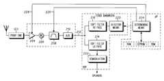
- FIG. 1shows a block diagram of a conventional dual mode radio frequency receiver.
- FIG. 2shows a block diagram of the backend portion of the receiver in accordance with the preferred embodiment of the present invention.
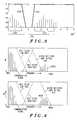
- FIG. 3shows the baseband frequency spectrum including the desired signal and the noise signal in accordance with the preferred embodiment of the present invention.
- FIG. 4shows the baseband frequency spectrum illustrating the active baseband filter settings.
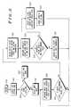
- FIG. 5is a flow chart illustrating the steps measuring and adjusting the gain accordingly in a trigger mode fashion in accordance with the preferred embodiment of the present invention.
- FIG. 6is s flow chart showing the steps of measuring and adjusting the gain in a sampling mode fashion in accordance with the preferred embodiment of the present invention.
- the present inventionprovides a unique method and apparatus to prevent power overload due to interfering noise present near the desired communication signal frequency in a multi mode receiver circuit for a wireless communications device.
- the dual mode receiverreceives radio frequency (RF) signals from a first bandwidth attuned to the advanced mobile phone system (AMPS) and a second bandwidth attuned to the global system for mobile communication (GSM) in a portable wireless radiotelephone.
- RFradio frequency
- the present inventionimproves the current method of controlling aggregate received power in the receiver using existing components necessary in dual mode communication device and eliminating the need for additional circuitry used in prior methods. Instead of adding circuitry, which in turn adds cost and increases the device size, the present invention advantageously utilizes the existing circuitry in combination with software solutions for the processing of the RF signals from multiple bandwidths necessary in a dual mode communication device.
- FIG. 1a block diagram of a wireless communication device in accordance with the preferred embodiment of the present invention is shown.
- This deviceis a cellular radiotelephone incorporating the present invention.
- a frame generator ASIC 101such as a CMOS ASIC available from Motorola, Inc.
- a microprocessor 103such as a 68HC11 microprocessor also available from Motorola, Inc., combine to generate the necessary communication protocol for operating in a cellular system.
- Microprocessor 103uses memory 104 comprising RAM 105 , EEPROM 107 , and ROM 109 , preferably consolidated in one package 111 , to execute the steps necessary to generate the protocol and to perform other functions for the wireless communication device, such as writing to a display 113 , accepting information from a keypad 115 , or controlling a frequency synthesizer 125 and DSP 106 which includes controlling receiver gain in accordance with the present invention.
- ASIC 101processes audio transformed by audio circuitry 119 from a microphone 117 and to a speaker 121 .
- FIG. 1also shows the front end receiver circuitry 123 which is capable of receiving RF signals from two distinct bandwidths which is required for operation of a dual mode communication device.
- the front end receiveris comprised of two channels: channel one 149 for operating in a first desired mode and channel two 151 for operating in a second desired mode.
- channel one 149is attuned to receive AMPS communication signals
- channel two 151is attuned to receive GSM communication signals.
- the AMPS communication systemoperates from 824 MHz to 894 MHz, which is subdivided into 30 kHz channels.
- the GSM communication systemoperates in the 1850 MHz to 1990 MHz subdivided into 200 kHz channels.
- the IF switch 135will be programmed to the appropriate corresponding channel.
- the IF switch 135is coupled to a synthesizer 125 which performs baseband (BB) conversion and appropriate active filtering which is necessary for demodulation of the desired communication signal.
- BBbaseband
- the synthesizer 125 , DSP 106 , and microprocessor 103are shown in greater detail in the block diagrams of FIG. 2 .
- the synthesizercontains an IF pre-amp 204 , an IF mixer 206 , an active baseband (BB) filter 208 , and an analog to digital converter 210 .
- IF pre-amp 204provides automatic gain control (AGC) means to control the aggregate signal gain input to the BB mixer 206 and the active BB filter 208 as both are susceptible to overload.
- AGC 204 circuit thereformaintains the BB circuitry power level within the designed operating range so the receiver may function properly.
- the BB mixerconverts the IF signal into a second IF frequency which is then subsequently filtered by active BB filter 208 .
- Active BB filter 208functions to allow only the desired communication signal to pass for further processing.
- the size of the bandwidthis adjustable in response to control signals sent by the microprocessor 103 . While receiving a desired communication signal the active BB filter 208 bandwidth is set accordingly and extraneous noise near the desired communication signal is filtered out as much as possible by the active BB filter 208 . All unwanted noise however can not be filtered and residual noise passes on to further processing.
- the signalis converted to a digital signal by the analog to digital converter 210 .
- This convertertakes all signals (desired communication signal and noise) and converts them to digital data bits which are then passed on to the DSP 106 via a serial data link 212 for additional soft filtering and demodulation.
- FIG. 2further shows the DSP in which the digital data signal is split into two channels from a common node.
- a first receiving channelwhich is comprised of a first soft filter 214 and a second receiving channel, which is comprised of a second soft filter 216 , both channels processing the incoming signal simultaneously.
- the first soft filter 214is a low pass filter and processes the desired AMPS communication signal bandwidth.
- the second soft filter 216is programmed as a high pass filter, attenuating the desired AMPS communication signal while allowing the undesired noise to pass through to the detector 220 .
- FIG. 3shows the desired communication signal 302 and the undesired noise 304 at baseband frequencies.
- the combination of the desired communication signal 302 and the undesired noise 304is the aggregate received signal 310 .
- FIG. 3also shows the DSP low pass soft filter response 308 and the DSP high pass soft filter response 306 .
- the detector 220estimates the power of said undesired noise 304 passed though the high pass soft filter 216 and provides this estimate to the determining means 224 in the microprocessor 103 .
- the determining means 224 in the microprocessor 103compares the undesired noise 304 level to a first predetermined noise level. If the undesired noise 304 level is greater than the first predetermined noise level, the determining means sends a signal to the active BB filter 208 to increase the BB bandwidth from the AMPS setting to the GSM setting.
- FIG. 4shows in accordance with the preferred embodiment of the present invention the BB bandwidth 410 of 15 kHz for the AMPS setting and the BB bandwidth 412 of 100 kHz for the GSM setting. Once the BB bandwidth is increased, the detector 220 makes a second power estimation of the undesired noise 304 passing through the high pass soft filter 216 and provides the estimate to the determining means in the microprocessor 103 .
- the determining meanssends a signal 228 to the AGC 204 to reduce the aggregate received signal power.
- the amount the aggregate received signal 310 power is reducedis inversely proportional to the estimated noise power level. The higher the estimated undesired noise 304 level, the greater the reduction in the aggregate received signal 310 power.
- FIG. 5shows a flowchart of the preferred steps for triggering noise measurements in the present invention.
- the receiverchecks the mode of operation in step 502 . If the receiver is in AMPS mode the receiver continues to step 508 , which is to measure the noise level passing through said second soft filter 216 . The communication device will then determine if the measured noise level is greater than a first predetermined noise level at step 510 . If the noise level is greater than the predetermined value, this indicates there may be more noise present but since the active BB filter 208 is attuned to the bandwidth required for AMPS mode, some of the interfering noise is attenuated by the active BB filter 208 and therefor cannot pass to the second soft filter.
- the communication devicemakes the decision to increase the bandwidth of the active filter 208 which corresponds to step 512 .
- the bandwidth of the active BB filter 208is increase any noise initially outside of the bandwidth will now be captured and measured at step 516 .
- the communication devicewill compare the noise level of the increased bandwidth to a second predetermined noise level. This measurement gives a better estimate of the power input to the IF mixer 206 and the active BB filter 208 . If this level is greater than the second predetermined noise level, which is equal to the minimum receiver sensitivity, the communication device will select a necessary AGC setting in accordance with the measured noise value at step 520 .
- the microprocessor 103then sends a corresponding signal to the AGC to reduce the gain into the IF mixer 206 and the active filter 208 to assure that these circuits are not saturated.
- FIG. 6a second flow chart shows the preferred steps of sampling noise levels and adjusting incoming power according to the present invention.
- the communication devicechecks the mode of operation in step. 502 . If the mode is AMPS, the device generates a random time delay between one and two seconds for selecting an a periodic sampling rate. The device then proceeds to step 610 and starts a countdown timer. Once the countdown timer reaches zero in step 612 , the device sends a signal to the active BB filter 208 to increase the bandwidth to include the bandwidth attuned to the GSM mode. In accordance with the preferred embodiment of the present invention, the bandwidth increases from 15 kHz to 100 kHz.
- the detector 220estimates the noise power level passed through soft filter 216 and sends this information to the microprocessor 103 .
- the estimated noise power levelis compared to the second predetermined power level at step 618 . If the estimated noise power level is greater than said second predetermined power level, the device proceeds to step 620 and calculates an AGC adjustment level based on the estimated noise power level. The device then sends a corresponding signal to the AGC and the incoming aggregate signal power is adjusted accordingly. If the noise level measured in step 616 is less than the second predetermined noise level, then the device proceeds to step 628 and returns the active BB filter 208 to the first bandwidth attuned to the AMPS mode and resumes normal operation.
- the noiseis measured coincidentally with the processing of the desired communication signal.
- the first soft filterprocessing the desired communication signal, attenuates the noise, while the second soft filter of the second channel measures the noise level and makes the adjustments in accordance with the flow charts above.
- the present inventionfinds particular application in assuring that the incoming aggregate power level does not overload the baseband circuitry causing saturation.
- the method and apparatusprovides the gain control using the existing circuitry in dual mode communication device eliminating the need for additional circuitry hence saving space on the printed circuit board and within the integrated circuits.
- the ever increasing power of DSP technologyallows for the simultaneous measurements of the noise level and processing of the desired communication signal to provide seamless power control.
- the method and apparatusalso allows for greater control over the AGC adjustment level as the level is calculated based on the measured aggregate power level as opposed to using predetermined AGC adjustment level.
Landscapes
- Engineering & Computer Science (AREA)
- Computer Networks & Wireless Communication (AREA)
- Signal Processing (AREA)
- Noise Elimination (AREA)
- Circuits Of Receivers In General (AREA)
- Input Circuits Of Receivers And Coupling Of Receivers And Audio Equipment (AREA)
- Transceivers (AREA)
Abstract
Description
The present invention relates to the control of radio frequency (RF) signal power received in a multi band receiver. More particularly the invention relates to a method and apparatus for detection of interference energy from RF signals present in adjacent bandwidths and controlling the energy received in the baseband portion of the receiver to ensure that said baseband circuitry is not saturated or overdriven.
A dual mode communication device is designed to transmit and receive RF signals of either an analog or a digital nature. The method for transmitting analog RF signals is typically achieved using the advanced mobile phone system (AMPS) and the transmission method of digital RF signals may be chosen from a plurality of multiple access techniques including time division multiple access (TDMA), code division multiple access (CDMA), and global system for mobile communication (GSM). A multi mode device such as a dual mode device will combine some of these techniques and incorporate them into one device. The receiver portion of a dual mode communication device for example, is similar to those which are not dual mode but are adapted to receive a combination of signals in accordance with any two of the methods above, analog or digital.
Typical receiver circuitry comprises two general portions: a front end portion and a back end portion. The front end portion functions to perform initial filtering, amplification of the desired bandwidth, and conversion to an intermediate frequency for further processing by the backend portion of the receiver. The backend portion converts the signal to the baseband in preparation for digital signal processing. RF signals enter the front end portion via the antenna and are transferred from the front end to the back end.
Controlling the incoming signal power of a radio frequency receiver is essential to proper operation of the receiver as the control functions to maintain signal levels within the operating range of the baseband circuitry. If the signal level exceeds the operating range of said baseband circuitry, the receiver performance degrades as a result of the decreasing signal to noise ratio and receiver selectivity. This may occur when interfering adjacent signals are very strong compared to the desired on-channel signal and the baseband circuitry becomes saturated as a result of the overload. This results in the desired on-channel signal becoming desensitized. Therefore, it is necessary to control the received signal power prior to the baseband circuitry and maintain signal levels within the back end circuit's operating range. Filter portions of the baseband circuitry reduce the adjacent interference noise signals by allowing only the desired on-channel frequency to pass through. However, the incoming aggregate power level prior to the baseband circuitry comprises the desired communication signal as well as the interfering noise energy. The combination of these two can lead to saturation of the baseband circuitry as a result of the noise level becoming too high.
One typical method of control is to provide measurement circuitry prior to the baseband circuitry such that a power estimation of the interfering noise level can be made. A conventional means for power estimation is to measure the aggregate received power level and provides measurement data to the received signal strength indicator (RSSI). The RSSI through additional circuitry, provides a control signal to the automatic gain control (AGC) corresponding to the estimated power level. The signal provided to the AGC from the RSSI is used to control the gain of the aggregate received power level entering the baseband circuitry. As the aggregate received power level increases, the AGC reduces the signal gain. This provides control of the incoming signal power but is performed with the disadvantages of additional cost of extra circuitry, increased integrated circuit (IC) size, and increased land requirement on the printed circuit board (PCB).
The use of additional circuitry poses a problem as this requires more space within the device and cost reduction is almost always desired. Therefore, there is a need to improve the means and method of detecting and controlling the noise entering the receiver.
FIG. 1 shows a block diagram of a conventional dual mode radio frequency receiver.
FIG. 2 shows a block diagram of the backend portion of the receiver in accordance with the preferred embodiment of the present invention.
FIG. 3 shows the baseband frequency spectrum including the desired signal and the noise signal in accordance with the preferred embodiment of the present invention.
FIG. 4 shows the baseband frequency spectrum illustrating the active baseband filter settings.
FIG. 5 is a flow chart illustrating the steps measuring and adjusting the gain accordingly in a trigger mode fashion in accordance with the preferred embodiment of the present invention.
FIG. 6 is s flow chart showing the steps of measuring and adjusting the gain in a sampling mode fashion in accordance with the preferred embodiment of the present invention.
The present invention provides a unique method and apparatus to prevent power overload due to interfering noise present near the desired communication signal frequency in a multi mode receiver circuit for a wireless communications device. In the preferred embodiment of the present invention the dual mode receiver receives radio frequency (RF) signals from a first bandwidth attuned to the advanced mobile phone system (AMPS) and a second bandwidth attuned to the global system for mobile communication (GSM) in a portable wireless radiotelephone.
All receivers whether they are single mode, dual mode, or multi mode require some means to maintain the level of the received RF signal within the operating range of the receiver circuitry. The present invention improves the current method of controlling aggregate received power in the receiver using existing components necessary in dual mode communication device and eliminating the need for additional circuitry used in prior methods. Instead of adding circuitry, which in turn adds cost and increases the device size, the present invention advantageously utilizes the existing circuitry in combination with software solutions for the processing of the RF signals from multiple bandwidths necessary in a dual mode communication device.
Turning to FIG. 1, a block diagram of a wireless communication device in accordance with the preferred embodiment of the present invention is shown. This device is a cellular radiotelephone incorporating the present invention. In the preferred embodiment a frame generator ASIC101, such as a CMOS ASIC available from Motorola, Inc. and amicroprocessor 103, such as a 68HC11 microprocessor also available from Motorola, Inc., combine to generate the necessary communication protocol for operating in a cellular system.Microprocessor 103 usesmemory 104 comprisingRAM 105, EEPROM107, andROM 109, preferably consolidated in onepackage 111, to execute the steps necessary to generate the protocol and to perform other functions for the wireless communication device, such as writing to adisplay 113, accepting information from akeypad 115, or controlling afrequency synthesizer 125 and DSP106 which includes controlling receiver gain in accordance with the present invention. ASIC101 processes audio transformed byaudio circuitry 119 from amicrophone 117 and to aspeaker 121.
FIG. 1 also shows the frontend receiver circuitry 123 which is capable of receiving RF signals from two distinct bandwidths which is required for operation of a dual mode communication device. The front end receiver is comprised of two channels: channel one149 for operating in a first desired mode and channel two151 for operating in a second desired mode. In accordance with the preferred embodiment of the present invention, channel one149 is attuned to receive AMPS communication signals and channel two151 is attuned to receive GSM communication signals. The AMPS communication system operates from 824 MHz to 894 MHz, which is subdivided into 30 kHz channels. The GSM communication system operates in the 1850 MHz to 1990 MHz subdivided into 200 kHz channels. Depending on the operation mode of the communication device, theIF switch 135 will be programmed to the appropriate corresponding channel. TheIF switch 135 is coupled to asynthesizer 125 which performs baseband (BB) conversion and appropriate active filtering which is necessary for demodulation of the desired communication signal.
Thesynthesizer 125, DSP106, andmicroprocessor 103 are shown in greater detail in the block diagrams of FIG.2. The synthesizer contains an IF pre-amp204, anIF mixer 206, an active baseband (BB)filter 208, and an analog todigital converter 210. IF pre-amp204 provides automatic gain control (AGC) means to control the aggregate signal gain input to theBB mixer 206 and theactive BB filter 208 as both are susceptible to overload. The AGC204 circuit therefor maintains the BB circuitry power level within the designed operating range so the receiver may function properly. The BB mixer converts the IF signal into a second IF frequency which is then subsequently filtered byactive BB filter 208.Active BB filter 208 functions to allow only the desired communication signal to pass for further processing. The size of the bandwidth is adjustable in response to control signals sent by themicroprocessor 103. While receiving a desired communication signal theactive BB filter 208 bandwidth is set accordingly and extraneous noise near the desired communication signal is filtered out as much as possible by theactive BB filter 208. All unwanted noise however can not be filtered and residual noise passes on to further processing.
Once the desired signal is filtered by theactive BB filter 208 the signal is converted to a digital signal by the analog todigital converter 210. This converter takes all signals (desired communication signal and noise) and converts them to digital data bits which are then passed on to the DSP106 via aserial data link 212 for additional soft filtering and demodulation.
FIG. 2 further shows the DSP in which the digital data signal is split into two channels from a common node. A first receiving channel, which is comprised of a firstsoft filter 214 and a second receiving channel, which is comprised of a secondsoft filter 216, both channels processing the incoming signal simultaneously. In accordance with the preferred embodiment of the present invention the firstsoft filter 214 is a low pass filter and processes the desired AMPS communication signal bandwidth. The secondsoft filter 216 is programmed as a high pass filter, attenuating the desired AMPS communication signal while allowing the undesired noise to pass through to thedetector 220. FIG. 3 shows the desired communication signal302 and theundesired noise 304 at baseband frequencies. The combination of the desired communication signal302 and theundesired noise 304 is the aggregate receivedsignal 310. FIG. 3 also shows the DSP low passsoft filter response 308 and the DSP high passsoft filter response 306. Thedetector 220 estimates the power of saidundesired noise 304 passed though the high passsoft filter 216 and provides this estimate to the determining means224 in themicroprocessor 103.
The determining means224 in themicroprocessor 103 compares theundesired noise 304 level to a first predetermined noise level. If theundesired noise 304 level is greater than the first predetermined noise level, the determining means sends a signal to theactive BB filter 208 to increase the BB bandwidth from the AMPS setting to the GSM setting. FIG. 4 shows in accordance with the preferred embodiment of the present invention theBB bandwidth 410 of 15 kHz for the AMPS setting and theBB bandwidth 412 of 100 kHz for the GSM setting. Once the BB bandwidth is increased, thedetector 220 makes a second power estimation of theundesired noise 304 passing through the high passsoft filter 216 and provides the estimate to the determining means in themicroprocessor 103.
If the estimated power level of theundesired noise 304 is greater than a second predetermined noise level, the determining means sends asignal 228 to theAGC 204 to reduce the aggregate received signal power. The amount the aggregate receivedsignal 310 power is reduced is inversely proportional to the estimated noise power level. The higher the estimatedundesired noise 304 level, the greater the reduction in the aggregate receivedsignal 310 power.
FIG. 5 shows a flowchart of the preferred steps for triggering noise measurements in the present invention. After beginning atstep 500, the receiver checks the mode of operation instep 502. If the receiver is in AMPS mode the receiver continues to step508, which is to measure the noise level passing through said secondsoft filter 216. The communication device will then determine if the measured noise level is greater than a first predetermined noise level atstep 510. If the noise level is greater than the predetermined value, this indicates there may be more noise present but since theactive BB filter 208 is attuned to the bandwidth required for AMPS mode, some of the interfering noise is attenuated by theactive BB filter 208 and therefor cannot pass to the second soft filter. In this case, the communication device makes the decision to increase the bandwidth of theactive filter 208 which corresponds to step512. Once the bandwidth of theactive BB filter 208 is increase any noise initially outside of the bandwidth will now be captured and measured atstep 516. Now the communication device will compare the noise level of the increased bandwidth to a second predetermined noise level. This measurement gives a better estimate of the power input to theIF mixer 206 and theactive BB filter 208. If this level is greater than the second predetermined noise level, which is equal to the minimum receiver sensitivity, the communication device will select a necessary AGC setting in accordance with the measured noise value atstep 520. Themicroprocessor 103 then sends a corresponding signal to the AGC to reduce the gain into theIF mixer 206 and theactive filter 208 to assure that these circuits are not saturated.
Turning to FIG. 6, a second flow chart shows the preferred steps of sampling noise levels and adjusting incoming power according to the present invention. As in FIG. 5, the communication device checks the mode of operation in step.502. If the mode is AMPS, the device generates a random time delay between one and two seconds for selecting an a periodic sampling rate. The device then proceeds to step610 and starts a countdown timer. Once the countdown timer reaches zero instep 612, the device sends a signal to theactive BB filter 208 to increase the bandwidth to include the bandwidth attuned to the GSM mode. In accordance with the preferred embodiment of the present invention, the bandwidth increases from 15 kHz to 100 kHz. Atstep 618 thedetector 220 estimates the noise power level passed throughsoft filter 216 and sends this information to themicroprocessor 103. In the microprocessor, the estimated noise power level is compared to the second predetermined power level atstep 618. If the estimated noise power level is greater than said second predetermined power level, the device proceeds to step620 and calculates an AGC adjustment level based on the estimated noise power level. The device then sends a corresponding signal to the AGC and the incoming aggregate signal power is adjusted accordingly. If the noise level measured instep 616 is less than the second predetermined noise level, then the device proceeds to step628 and returns theactive BB filter 208 to the first bandwidth attuned to the AMPS mode and resumes normal operation. Because the DSP processes the incoming signal in parallel, the noise is measured coincidentally with the processing of the desired communication signal. The first soft filter, processing the desired communication signal, attenuates the noise, while the second soft filter of the second channel measures the noise level and makes the adjustments in accordance with the flow charts above.
The present invention finds particular application in assuring that the incoming aggregate power level does not overload the baseband circuitry causing saturation. The method and apparatus provides the gain control using the existing circuitry in dual mode communication device eliminating the need for additional circuitry hence saving space on the printed circuit board and within the integrated circuits. The ever increasing power of DSP technology allows for the simultaneous measurements of the noise level and processing of the desired communication signal to provide seamless power control. The method and apparatus also allows for greater control over the AGC adjustment level as the level is calculated based on the measured aggregate power level as opposed to using predetermined AGC adjustment level.
Although the invention has been described and illustrated in the above description and drawings, it is understood that this description is by way of example only and that numerous changes and modifications can me made by those skilled in the art without departing from the true spirit and scope of the invention. For example, although method and apparatus for controlling incoming signal power into a RF device is shown, the device may also be a light based device receiving communication signals in the form of light waves. Although the present invention finds particular use in portable cellular radiotelephones, the invention could be applied to any wireless communication device, including pagers, electronic organizers, and computers. Applicant's invention should be limited only by the following claims.
Claims (13)
1. A method for preventing saturation of a radio frequency receiver having a first bandwidth comprising the steps of:
receiving an input communication signal from within said first bandwidth through a first receiving path;
measuring a noise level from within said first bandwidth through a second receiving path while coincidentally receiving said input communication signal through said first receiving path;
comparing said noise level of said second path to a first predetermined noise level; and
adjusting said first bandwidth to a second bandwidth which is greater than said first bandwidth in response to said comparing step determining that said noise level is greater than said first predetermined noise level.
2. The method ofclaim 1 further comprising the step of measuring said noise level from within said second bandwidth through said second receiving path in response to said comparing step determining that said noise level is greater than said first predetermined noise level, simultaneously with said input communication signal.
3. The method ofclaim 2 , further comprising the step of adjusting an incoming signal gain in response to said measuring step determining that said noise level of said measuring step is greater than a second predetermined noise level.
4. A receiver for receiving a communication signal, said communication signal having an aggregate received power level, said receiver comprising:
a first path for receiving a desired communication signal from within a first desired bandwidth, said desired communication signal having a noise level;
a second path for coincidentally receiving said noise level; and
determining means for determining said aggregate noise level of said second path.
5. The receiver ofclaim 4 further comprising a first adjusting means for increasing said first bandwidth to a second bandwidth in response to said determining means determining that said aggregate noise level is greater than a first predetermined noise level.
6. The receiver ofclaim 5 further comprising a second adjusting means coupled to said first adjusting means for adjusting said aggregate received power level in response to said determining means determining that said aggregate noise level form within said second bandwidth is greater than a second predetermined noise level.
7. A dual mode radio frequency receiver for receiving advanced mobile phone system (AMPS) communication signals and global system for mobile communications (GSM) communication signals, said receiver comprising:
a front end portion for receiving said AMPS and said GSM communication signals;
automatic gain control (AGC) means coupled to said front end for controlling an aggregate signal gain received from said front end;
active filter means coupled to said AGC and having a variable bandwidth, said variable bandwidth selectively adjustable to define a first bandwidth attuned with AMPS signal processing for allowing AMPS communication signals to pass therethrough and to define a second bandwidth attuned with GSM signal processing for allowing GSM communication signals to pass therethrough;
conversion means coupled to said active filter means for converting said GSM communication signal and converting said AMPS communication signal into digital signals and providing said digital signals to a node;
a low pass filter coupled to said node by a first channel, said first filter for further defining a first baseband;
a high pass filter coupled to said node by a second channel, said second filter for further defining a second baseband;
power estimating means coupled to the output of said high pass filter for estimating an undesired noise level; and
determining means coupled to said power estimating means for determining if said undesired noise level is greater than a first predetermined aggregate power level, and in response thereto sending a signal to said active filter to selectively adjust for a predetermined amount of time, from defining said first bandwidth to defining said second bandwidth.
8. The receiver ofclaim 7 wherein said determining means in response to determining that said undesired noise is greater than a second predetermined aggregate power level, sends a signal to said AGC to decrease said aggregate signal gain.
9. The receiver ofclaim 8 wherein said low pass filter is comprised of a first soft filter and said high pass filter is comprised of a second soft filter.
10. The receiver ofclaim 9 , wherein said second predetermined aggregate power level is less than or equal to a predetermined receiver sensitivity value.
11. A method for preventing saturation of a radio frequency receiver having a first bandwidth comprising the steps of:
receiving an input communication signal from within said first bandwidth through a first receiving path, said input communication having an aggregate received power level;
adjusting said first bandwidth to a second bandwidth having a greater frequency range than said first bandwidth;
measuring an aggregate noise level of said second bandwidth through a second receiving path, while concurrently receiving said input signal through said first path;
determining if said aggregate noise level of said second receiving path is greater than a predetermined aggregate noise level; and
adjusting said aggregate received power level in response to determining that said aggregate noise level of said second bandwidth is greater than said predetermined aggregate noise level.
12. The method ofclaim 11 wherein said adjusting and said measuring steps are performed at a randomly generated frequency.
13. A receiver for receiving a communication signal from a first desired bandwidth comprising:
a first path for receiving a desired communication signal from said first desired bandwidth, said desired communication signal having a noise level and an aggregate received power level;
an adjustable filter defining said first desired bandwidth and, adjustable to define a second bandwidth greater than said first bandwidth;
determining means for determining said noise level of said second bandwidth;
comparing means from comparing said noise level of said second bandwidth to a first predetermined noise level; and
adjusting means for adjusting said aggregate received power level in response to said comparing means determining that said noise level is greater than said first predetermined noise level.
Priority Applications (5)
| Application Number | Priority Date | Filing Date | Title |
|---|---|---|---|
| US09/478,224US6614806B1 (en) | 2000-01-06 | 2000-01-06 | Method and apparatus for interfering receiver signal overload protection |
| GB0031870AGB2360406B (en) | 2000-01-06 | 2000-12-23 | Method and apparatus for interfering receiver signal overload protection |
| JP2001000552AJP4459458B2 (en) | 2000-01-06 | 2001-01-05 | Method and apparatus for protection of jammed received signal overload |
| DE10100323ADE10100323B4 (en) | 2000-01-06 | 2001-01-05 | Method and device for protection against received signal overload |
| CN01100203.4ACN1227930C (en) | 2000-01-06 | 2001-01-05 | Overload protective method and device of receiver interference signal |
Applications Claiming Priority (1)
| Application Number | Priority Date | Filing Date | Title |
|---|---|---|---|
| US09/478,224US6614806B1 (en) | 2000-01-06 | 2000-01-06 | Method and apparatus for interfering receiver signal overload protection |
Publications (1)
| Publication Number | Publication Date |
|---|---|
| US6614806B1true US6614806B1 (en) | 2003-09-02 |
Family
ID=23899030
Family Applications (1)
| Application Number | Title | Priority Date | Filing Date |
|---|---|---|---|
| US09/478,224Expired - LifetimeUS6614806B1 (en) | 2000-01-06 | 2000-01-06 | Method and apparatus for interfering receiver signal overload protection |
Country Status (5)
| Country | Link |
|---|---|
| US (1) | US6614806B1 (en) |
| JP (1) | JP4459458B2 (en) |
| CN (1) | CN1227930C (en) |
| DE (1) | DE10100323B4 (en) |
| GB (1) | GB2360406B (en) |
Cited By (21)
| Publication number | Priority date | Publication date | Assignee | Title |
|---|---|---|---|---|
| US20010018752A1 (en)* | 2000-02-21 | 2001-08-30 | Matsushita Electric Industrial Co., Ltd | Apparatus and method for processing information continuously even against extraneously incoming noise |
| US20030199264A1 (en)* | 2002-04-09 | 2003-10-23 | Christian Holenstein | Direct current offset cancellation for mobile station modems using direct conversion |
| US20040021798A1 (en)* | 2002-07-31 | 2004-02-05 | Conexant Systems, Inc. | Integrated programmable tuner |
| US20040038650A1 (en)* | 2000-10-11 | 2004-02-26 | Bin Yang | Apparatus and method for signal strength compensation of highly-time-variant mobile radio channels and reception unit for mobile radio transmission |
| US20050079824A1 (en)* | 2003-10-09 | 2005-04-14 | Roland Rick | Cell selection techniques for frequency division multiple access systems |
| US20050078654A1 (en)* | 2003-10-09 | 2005-04-14 | Roland Rick | Parallel cell ID acquisition in frequency division multiple access systems |
| US20060008035A1 (en)* | 2004-07-01 | 2006-01-12 | Staccato Communications, Inc. | Payload boundary detection during multiband receiver synchronization |
| US20060046773A1 (en)* | 2004-08-26 | 2006-03-02 | Interdigital Technology Corporation | Method and apparatus for processing multiple wireless communication services |
| US20060045126A1 (en)* | 2004-08-30 | 2006-03-02 | Interdigital Technology Corporation | Method and apparatus for adaptively selecting sampling frequency for analog-to-digital conversion |
| US7116958B1 (en)* | 2002-08-02 | 2006-10-03 | Nortel Networks Limited | Interference rejection in a radio receiver |
| US20070047164A1 (en)* | 2005-08-26 | 2007-03-01 | Texas Instruments, Inc. | Transient triggered protection of IC components |
| US7292830B1 (en)* | 2004-03-31 | 2007-11-06 | Nortel Networks Limited | Receiver gain management |
| US20070265011A1 (en)* | 2006-05-11 | 2007-11-15 | Samsung Electronics Co., Ltd. | Wireless communication terminal and method for controlling power and using channel by adjusting channel bandwidth of wireless communication terminal |
| US7313099B2 (en) | 2002-06-28 | 2007-12-25 | Advanced Micro Devices, Inc. | Phase system rotation for power estimation |
| US20080014888A1 (en)* | 2006-07-17 | 2008-01-17 | M/A-Com, Inc. | Overload protection for receiver front end |
| US20080153447A1 (en)* | 2006-12-21 | 2008-06-26 | Nicholas Cowley | Techniques to deterministically reduce signal interference |
| US7605757B1 (en)* | 2007-05-31 | 2009-10-20 | Rockwell Collins, Inc. | Multiple signal receiver |
| US20110029790A1 (en)* | 2009-07-31 | 2011-02-03 | Broadcom Corporation | System and Method for Policing Bad Powered Devices in Power Over Ethernet |
| US20160241283A1 (en)* | 2012-05-21 | 2016-08-18 | L-3 Communications Corporation | Multiple interferer cancellation for communications systems |
| US9831836B1 (en) | 2016-10-07 | 2017-11-28 | Silicon Laboratories Inc. | Automatic gain control (AGC) circuit and method to control amplifier gain based on a duration of an overload condition |
| US10931321B1 (en)* | 2020-01-08 | 2021-02-23 | Eagle Technology, Llc | System and method for optimizing intermodulation performance of receivers |
Families Citing this family (8)
| Publication number | Priority date | Publication date | Assignee | Title |
|---|---|---|---|---|
| KR100539781B1 (en)* | 2003-02-22 | 2006-01-10 | 엘지전자 주식회사 | High frequency routing device and method of dual mode mobile terminal |
| GB2401498B (en) | 2003-05-07 | 2006-02-22 | Zarlink Semiconductor Ltd | Tuner |
| WO2006002508A1 (en)* | 2004-07-02 | 2006-01-12 | Research In Motion Limited | Rf test access for testing antenna in mobile communication device |
| US8929908B2 (en)* | 2005-10-27 | 2015-01-06 | Qualcomm Incorporated | Method and apparatus for estimating reverse link loading in a wireless communication system |
| CN101207858B (en)* | 2006-12-19 | 2010-12-01 | 中兴通讯股份有限公司 | Method of switch-in probe sending for eliminating other standard sending influence in double module mobile phone |
| US8019224B2 (en) | 2007-03-28 | 2011-09-13 | Seiko Epson Corporation | Communications device |
| US8213554B2 (en)* | 2008-01-29 | 2012-07-03 | Qualcomm Incorporated | Sparse sampling of signal innovations |
| US9673917B2 (en)* | 2008-05-30 | 2017-06-06 | Qualcomm Incorporated | Calibration using noise power |
Citations (34)
| Publication number | Priority date | Publication date | Assignee | Title |
|---|---|---|---|---|
| US3872387A (en)* | 1972-09-29 | 1975-03-18 | Zenith Radio Corp | Frequency response modifier for fixed-tuned IF amplifiers |
| US4355303A (en)* | 1981-04-09 | 1982-10-19 | Westinghouse Electric Corp. | Receiver for a distribution network power line carrier communication system |
| US4356568A (en)* | 1977-07-02 | 1982-10-26 | Nippon Gakki Seizo Kabushiki Kaisha | Receptive condition automatic selection device for FM receiver |
| US4356567A (en)* | 1977-06-28 | 1982-10-26 | Pioneer Electronic Corporation | Radio receiver with bandwidth switching |
| US4563651A (en)* | 1981-04-28 | 1986-01-07 | Oki Electric Industry Co., Ltd. | FM Demodulator with variable bandpass filter |
| US4792993A (en)* | 1985-10-30 | 1988-12-20 | Capetronic (Bsr) Ltd. | TVRD receiver system with automatic bandwidth adjustment |
| US5020092A (en) | 1989-06-23 | 1991-05-28 | Motorola, Inc. | Dual-bandwidth cellular telephone |
| US5060294A (en) | 1990-07-05 | 1991-10-22 | Motorola, Inc. | Dual mode power amplifier for radiotelephone |
| US5230098A (en)* | 1988-11-18 | 1993-07-20 | Fujitsu Limited | Relay receiver having a variable bandwidth |
| US5251331A (en) | 1992-03-13 | 1993-10-05 | Motorola, Inc. | High efficiency dual mode power amplifier apparatus |
| US5263055A (en)* | 1991-11-04 | 1993-11-16 | Motorola, Inc. | Apparatus and method for reducing harmonic interference generated by a clock signal |
| US5287556A (en)* | 1990-09-28 | 1994-02-15 | Motorola, Inc. | Interference reduction using an adaptive receiver filter, signal strength, and BER sensing |
| US5301364A (en)* | 1988-11-30 | 1994-04-05 | Motorola, Inc. | Method and apparatus for digital automatic gain control in a receiver |
| US5321851A (en)* | 1989-11-15 | 1994-06-14 | Sanyo Electric Co., Ltd. | Radio receiver comprising automatic gain controlling function |
| US5339454A (en)* | 1991-08-05 | 1994-08-16 | Ford Motor Company | Automatic gain control for RF amplifier |
| US5438684A (en) | 1992-03-13 | 1995-08-01 | Motorola, Inc. | Radio frequency signal power amplifier combining network |
| US5448763A (en)* | 1993-11-09 | 1995-09-05 | Motorola | Apparatus and method for operating a phase locked loop frequency synthesizer responsive to radio frequency channel spacing |
| EP0696852A2 (en) | 1994-08-11 | 1996-02-14 | Pioneer Electronic Corporation | FM receiver |
| US5598448A (en)* | 1995-03-06 | 1997-01-28 | Motorola Inc. | Method and apparatus for controlling a digital phase lock loop and within a cordless telephone |
| US5603115A (en)* | 1995-04-01 | 1997-02-11 | Hwa Lin Electronics Co., Ltd. | Direct broadcasting satellite tuner with an auto threshold control demodulator |
| US5604927A (en)* | 1993-12-24 | 1997-02-18 | U.S. Philips Corporation | Receiver having an adjustable bandwidth filter |
| US5630220A (en)* | 1992-05-22 | 1997-05-13 | Kabushiki Kaisha Toshiba | Automatic gain control circuit for radio communication apparatus |
| US5691666A (en)* | 1995-06-07 | 1997-11-25 | Owen; Joseph C. | Full threshold FM deviation compression feedback demodulator and method |
| US5715282A (en)* | 1996-05-08 | 1998-02-03 | Motorola, Inc. | Method and apparatus for detecting interference in a receiver for use in a wireless communication system |
| US5732341A (en)* | 1994-12-16 | 1998-03-24 | Qualcomm Incorporated | Method and apparatus for increasing receiver immunity to interference |
| US5734974A (en)* | 1996-03-27 | 1998-03-31 | Motorola, Inc. | Selective call receivers with stepwise variable gain control |
| US5828672A (en)* | 1997-04-30 | 1998-10-27 | Telefonaktiebolaget Lm Ericsson (Publ) | Estimation of radio channel bit error rate in a digital radio telecommunication network |
| US5862465A (en)* | 1996-01-29 | 1999-01-19 | Oki Electric Industry Co., Ltd. | Hysteresis-free anti-saturation circuit |
| US5898699A (en)* | 1996-06-28 | 1999-04-27 | Sony Corporation | Digital broadcast receiver and signal level display method |
| US5949832A (en)* | 1996-03-26 | 1999-09-07 | Sicom, Inc. | Digital receiver with tunable analog filter and method therefor |
| US6009129A (en)* | 1997-02-28 | 1999-12-28 | Nokia Mobile Phones | Device and method for detection and reduction of intermodulation distortion |
| US6070062A (en)* | 1997-03-28 | 2000-05-30 | Matsushita Electric Industrial Co., Ltd. | Mobile radio wave receiver with adaptive automatic gain control |
| US6442143B1 (en)* | 1999-09-30 | 2002-08-27 | Lockheed Martin Corporation | Signal quality maintenance in a communication system |
| US6476681B1 (en)* | 1998-08-11 | 2002-11-05 | Denso International America, Inc. | Adjustable bandwidth phase locked loop with fast settling time |
- 2000
- 2000-01-06USUS09/478,224patent/US6614806B1/ennot_activeExpired - Lifetime
- 2000-12-23GBGB0031870Apatent/GB2360406B/ennot_activeExpired - Lifetime
- 2001
- 2001-01-05JPJP2001000552Apatent/JP4459458B2/ennot_activeExpired - Fee Related
- 2001-01-05CNCN01100203.4Apatent/CN1227930C/ennot_activeExpired - Fee Related
- 2001-01-05DEDE10100323Apatent/DE10100323B4/ennot_activeExpired - Fee Related
Patent Citations (34)
| Publication number | Priority date | Publication date | Assignee | Title |
|---|---|---|---|---|
| US3872387A (en)* | 1972-09-29 | 1975-03-18 | Zenith Radio Corp | Frequency response modifier for fixed-tuned IF amplifiers |
| US4356567A (en)* | 1977-06-28 | 1982-10-26 | Pioneer Electronic Corporation | Radio receiver with bandwidth switching |
| US4356568A (en)* | 1977-07-02 | 1982-10-26 | Nippon Gakki Seizo Kabushiki Kaisha | Receptive condition automatic selection device for FM receiver |
| US4355303A (en)* | 1981-04-09 | 1982-10-19 | Westinghouse Electric Corp. | Receiver for a distribution network power line carrier communication system |
| US4563651A (en)* | 1981-04-28 | 1986-01-07 | Oki Electric Industry Co., Ltd. | FM Demodulator with variable bandpass filter |
| US4792993A (en)* | 1985-10-30 | 1988-12-20 | Capetronic (Bsr) Ltd. | TVRD receiver system with automatic bandwidth adjustment |
| US5230098A (en)* | 1988-11-18 | 1993-07-20 | Fujitsu Limited | Relay receiver having a variable bandwidth |
| US5301364A (en)* | 1988-11-30 | 1994-04-05 | Motorola, Inc. | Method and apparatus for digital automatic gain control in a receiver |
| US5020092A (en) | 1989-06-23 | 1991-05-28 | Motorola, Inc. | Dual-bandwidth cellular telephone |
| US5321851A (en)* | 1989-11-15 | 1994-06-14 | Sanyo Electric Co., Ltd. | Radio receiver comprising automatic gain controlling function |
| US5060294A (en) | 1990-07-05 | 1991-10-22 | Motorola, Inc. | Dual mode power amplifier for radiotelephone |
| US5287556A (en)* | 1990-09-28 | 1994-02-15 | Motorola, Inc. | Interference reduction using an adaptive receiver filter, signal strength, and BER sensing |
| US5339454A (en)* | 1991-08-05 | 1994-08-16 | Ford Motor Company | Automatic gain control for RF amplifier |
| US5263055A (en)* | 1991-11-04 | 1993-11-16 | Motorola, Inc. | Apparatus and method for reducing harmonic interference generated by a clock signal |
| US5251331A (en) | 1992-03-13 | 1993-10-05 | Motorola, Inc. | High efficiency dual mode power amplifier apparatus |
| US5438684A (en) | 1992-03-13 | 1995-08-01 | Motorola, Inc. | Radio frequency signal power amplifier combining network |
| US5630220A (en)* | 1992-05-22 | 1997-05-13 | Kabushiki Kaisha Toshiba | Automatic gain control circuit for radio communication apparatus |
| US5448763A (en)* | 1993-11-09 | 1995-09-05 | Motorola | Apparatus and method for operating a phase locked loop frequency synthesizer responsive to radio frequency channel spacing |
| US5604927A (en)* | 1993-12-24 | 1997-02-18 | U.S. Philips Corporation | Receiver having an adjustable bandwidth filter |
| EP0696852A2 (en) | 1994-08-11 | 1996-02-14 | Pioneer Electronic Corporation | FM receiver |
| US5732341A (en)* | 1994-12-16 | 1998-03-24 | Qualcomm Incorporated | Method and apparatus for increasing receiver immunity to interference |
| US5598448A (en)* | 1995-03-06 | 1997-01-28 | Motorola Inc. | Method and apparatus for controlling a digital phase lock loop and within a cordless telephone |
| US5603115A (en)* | 1995-04-01 | 1997-02-11 | Hwa Lin Electronics Co., Ltd. | Direct broadcasting satellite tuner with an auto threshold control demodulator |
| US5691666A (en)* | 1995-06-07 | 1997-11-25 | Owen; Joseph C. | Full threshold FM deviation compression feedback demodulator and method |
| US5862465A (en)* | 1996-01-29 | 1999-01-19 | Oki Electric Industry Co., Ltd. | Hysteresis-free anti-saturation circuit |
| US5949832A (en)* | 1996-03-26 | 1999-09-07 | Sicom, Inc. | Digital receiver with tunable analog filter and method therefor |
| US5734974A (en)* | 1996-03-27 | 1998-03-31 | Motorola, Inc. | Selective call receivers with stepwise variable gain control |
| US5715282A (en)* | 1996-05-08 | 1998-02-03 | Motorola, Inc. | Method and apparatus for detecting interference in a receiver for use in a wireless communication system |
| US5898699A (en)* | 1996-06-28 | 1999-04-27 | Sony Corporation | Digital broadcast receiver and signal level display method |
| US6009129A (en)* | 1997-02-28 | 1999-12-28 | Nokia Mobile Phones | Device and method for detection and reduction of intermodulation distortion |
| US6070062A (en)* | 1997-03-28 | 2000-05-30 | Matsushita Electric Industrial Co., Ltd. | Mobile radio wave receiver with adaptive automatic gain control |
| US5828672A (en)* | 1997-04-30 | 1998-10-27 | Telefonaktiebolaget Lm Ericsson (Publ) | Estimation of radio channel bit error rate in a digital radio telecommunication network |
| US6476681B1 (en)* | 1998-08-11 | 2002-11-05 | Denso International America, Inc. | Adjustable bandwidth phase locked loop with fast settling time |
| US6442143B1 (en)* | 1999-09-30 | 2002-08-27 | Lockheed Martin Corporation | Signal quality maintenance in a communication system |
Cited By (43)
| Publication number | Priority date | Publication date | Assignee | Title |
|---|---|---|---|---|
| US6721903B2 (en)* | 2000-02-21 | 2004-04-13 | Matsushita Electric Industrial Co., Ltd. | Apparatus and method for processing information continuously even against extraneously incoming noise |
| US20010018752A1 (en)* | 2000-02-21 | 2001-08-30 | Matsushita Electric Industrial Co., Ltd | Apparatus and method for processing information continuously even against extraneously incoming noise |
| US7092706B2 (en)* | 2000-10-11 | 2006-08-15 | Infineon Technologies Ag | Apparatus and method for signal strength compensation of highly time-variant mobile radio channels and reception unit for mobile radio transmission |
| US20040038650A1 (en)* | 2000-10-11 | 2004-02-26 | Bin Yang | Apparatus and method for signal strength compensation of highly-time-variant mobile radio channels and reception unit for mobile radio transmission |
| US6985711B2 (en)* | 2002-04-09 | 2006-01-10 | Qualcomm, Incorporated | Direct current offset cancellation for mobile station modems using direct conversion |
| US20030199264A1 (en)* | 2002-04-09 | 2003-10-23 | Christian Holenstein | Direct current offset cancellation for mobile station modems using direct conversion |
| US7313099B2 (en) | 2002-06-28 | 2007-12-25 | Advanced Micro Devices, Inc. | Phase system rotation for power estimation |
| US20040021798A1 (en)* | 2002-07-31 | 2004-02-05 | Conexant Systems, Inc. | Integrated programmable tuner |
| US7414676B2 (en)* | 2002-07-31 | 2008-08-19 | Conexant Systems, Inc. | Integrated programmable tuner |
| US7116958B1 (en)* | 2002-08-02 | 2006-10-03 | Nortel Networks Limited | Interference rejection in a radio receiver |
| WO2005036915A3 (en)* | 2003-10-09 | 2005-09-09 | Qualcomm Inc | Cell selection techniques for frequency division multiple access systems |
| US20050079824A1 (en)* | 2003-10-09 | 2005-04-14 | Roland Rick | Cell selection techniques for frequency division multiple access systems |
| EP2139131A1 (en)* | 2003-10-09 | 2009-12-30 | Qualcomm Incorporated | Cell selection techniques for frequency division multiple access systems |
| US7620029B2 (en) | 2003-10-09 | 2009-11-17 | Qualcomm Incorporated | Parallel cell ID acquisition in frequency division multiple access systems |
| RU2341916C2 (en)* | 2003-10-09 | 2008-12-20 | Квэлкомм Инкорпорейтед | Method and device for selecting interval in given frequency spectrum for frequency division multiple access systems |
| US20050078654A1 (en)* | 2003-10-09 | 2005-04-14 | Roland Rick | Parallel cell ID acquisition in frequency division multiple access systems |
| US20080089310A1 (en)* | 2003-10-09 | 2008-04-17 | Qualcomm Incorporated | Cell selection techniques for frequency division multiple access systems |
| US7321749B2 (en) | 2003-10-09 | 2008-01-22 | Qualcomm Incorporated | Cell selection techniques for frequency division multiple access systems |
| US7292830B1 (en)* | 2004-03-31 | 2007-11-06 | Nortel Networks Limited | Receiver gain management |
| US7634034B2 (en) | 2004-07-01 | 2009-12-15 | Staccato Communications, Inc. | Payload boundary detection during multiband receiver synchronization |
| US20060007986A1 (en)* | 2004-07-01 | 2006-01-12 | Staccato Communications, Inc. | Packet detection during multiband receiver synchronization |
| US20060008035A1 (en)* | 2004-07-01 | 2006-01-12 | Staccato Communications, Inc. | Payload boundary detection during multiband receiver synchronization |
| US20060007985A1 (en)* | 2004-07-01 | 2006-01-12 | Staccato Communications, Inc. | Saturation handling during multiband receiver synchronization |
| US20060046773A1 (en)* | 2004-08-26 | 2006-03-02 | Interdigital Technology Corporation | Method and apparatus for processing multiple wireless communication services |
| US9602144B2 (en)* | 2004-08-26 | 2017-03-21 | Interdigital Technology Corporation | Method and apparatus for processing multiple wireless communication services |
| US20060045126A1 (en)* | 2004-08-30 | 2006-03-02 | Interdigital Technology Corporation | Method and apparatus for adaptively selecting sampling frequency for analog-to-digital conversion |
| US7551413B2 (en)* | 2005-08-26 | 2009-06-23 | Texas Instruments Incorporated | Transient triggered protection of IC components |
| US20070047164A1 (en)* | 2005-08-26 | 2007-03-01 | Texas Instruments, Inc. | Transient triggered protection of IC components |
| US20070265011A1 (en)* | 2006-05-11 | 2007-11-15 | Samsung Electronics Co., Ltd. | Wireless communication terminal and method for controlling power and using channel by adjusting channel bandwidth of wireless communication terminal |
| US7706752B2 (en)* | 2006-05-11 | 2010-04-27 | Samsung Electronics Co., Ltd. | Wireless communication terminal and method for controlling power and using channel by adjusting channel bandwidth of wireless communication terminal |
| US20080014888A1 (en)* | 2006-07-17 | 2008-01-17 | M/A-Com, Inc. | Overload protection for receiver front end |
| US7599674B2 (en) | 2006-07-17 | 2009-10-06 | Pine Valley Investments, Inc. | Overload protection for receiver front end |
| US20080153447A1 (en)* | 2006-12-21 | 2008-06-26 | Nicholas Cowley | Techniques to deterministically reduce signal interference |
| US7693501B2 (en)* | 2006-12-21 | 2010-04-06 | Intel Corporation | Techniques to deterministically reduce signal interference |
| US7605757B1 (en)* | 2007-05-31 | 2009-10-20 | Rockwell Collins, Inc. | Multiple signal receiver |
| US8301922B2 (en)* | 2009-07-31 | 2012-10-30 | Broadcom Corporation | System and method for policing bad powered devices in power over ethernet |
| US20110029790A1 (en)* | 2009-07-31 | 2011-02-03 | Broadcom Corporation | System and Method for Policing Bad Powered Devices in Power Over Ethernet |
| US20160241283A1 (en)* | 2012-05-21 | 2016-08-18 | L-3 Communications Corporation | Multiple interferer cancellation for communications systems |
| US9577687B2 (en)* | 2012-05-21 | 2017-02-21 | L-3 Communications Corporation | Multiple interferer cancellation for communications systems |
| US9748987B2 (en) | 2012-05-21 | 2017-08-29 | L3 Technologies, Inc. | Interference cancellation system for cancelling interference in the optical domain |
| US9831901B2 (en) | 2012-05-21 | 2017-11-28 | L3 Technologies, Inc. | Remote interference cancellation for communications systems |
| US9831836B1 (en) | 2016-10-07 | 2017-11-28 | Silicon Laboratories Inc. | Automatic gain control (AGC) circuit and method to control amplifier gain based on a duration of an overload condition |
| US10931321B1 (en)* | 2020-01-08 | 2021-02-23 | Eagle Technology, Llc | System and method for optimizing intermodulation performance of receivers |
Also Published As
| Publication number | Publication date |
|---|---|
| DE10100323B4 (en) | 2012-11-08 |
| JP4459458B2 (en) | 2010-04-28 |
| JP2001230686A (en) | 2001-08-24 |
| GB2360406B (en) | 2002-07-03 |
| DE10100323A1 (en) | 2001-09-20 |
| CN1303223A (en) | 2001-07-11 |
| CN1227930C (en) | 2005-11-16 |
| GB0031870D0 (en) | 2001-02-14 |
| GB2360406A (en) | 2001-09-19 |
Similar Documents
| Publication | Publication Date | Title |
|---|---|---|
| US6614806B1 (en) | Method and apparatus for interfering receiver signal overload protection | |
| KR100746608B1 (en) | Apparatus for increasing receiver sensitivity of receiver for direct conversion, and related methods | |
| JP3989572B2 (en) | Apparatus and method for optimizing received signal quality in a radio receiver | |
| US6324387B1 (en) | LNA control-circuit for receive closed loop automatic gain control | |
| JP4234615B2 (en) | Method and apparatus for improving receiver interference immunity | |
| US6801760B2 (en) | Control of receiver immunity to interference by controlling linearity | |
| US20040033789A1 (en) | Dynamic frequency selection and radar detection with a wireless LAN | |
| JP4250137B2 (en) | Apparatus and method for reducing monitoring in uplink compressed mode in communication apparatus | |
| JPH11317690A (en) | Adaptive control technique of receiver linearity for radio transceiver | |
| JP4706871B2 (en) | Diversity receiving apparatus and gain adjusting method thereof | |
| EP1061643B1 (en) | Receiver and gain control method of the same | |
| JP4463332B2 (en) | Method and apparatus for increasing interfering receiver immunity | |
| JPH07240702A (en) | Spread spectrum communication device | |
| JP2000068870A (en) | Receiver and method for preventing intermodulation | |
| KR100693556B1 (en) | LS control method of mobile communication terminal | |
| JP2004128863A (en) | Wireless communication device | |
| JP2000299643A (en) | Receiver |
Legal Events
| Date | Code | Title | Description |
|---|---|---|---|
| AS | Assignment | Owner name:MOTOROLA, INC, ILLINOIS Free format text:ASSIGNMENT OF ASSIGNORS INTEREST;ASSIGNOR:NANNI, PETER;REEL/FRAME:010487/0403 Effective date:20000106 | |
| STCF | Information on status: patent grant | Free format text:PATENTED CASE | |
| FPAY | Fee payment | Year of fee payment:4 | |
| AS | Assignment | Owner name:MOTOROLA MOBILITY, INC, ILLINOIS Free format text:ASSIGNMENT OF ASSIGNORS INTEREST;ASSIGNOR:MOTOROLA, INC;REEL/FRAME:025673/0558 Effective date:20100731 | |
| FPAY | Fee payment | Year of fee payment:8 | |
| AS | Assignment | Owner name:MOTOROLA MOBILITY LLC, ILLINOIS Free format text:CHANGE OF NAME;ASSIGNOR:MOTOROLA MOBILITY, INC.;REEL/FRAME:029216/0282 Effective date:20120622 | |
| AS | Assignment | Owner name:GOOGLE TECHNOLOGY HOLDINGS LLC, CALIFORNIA Free format text:ASSIGNMENT OF ASSIGNORS INTEREST;ASSIGNOR:MOTOROLA MOBILITY LLC;REEL/FRAME:034430/0001 Effective date:20141028 | |
| FPAY | Fee payment | Year of fee payment:12 |