US6614692B2 - EEPROM array and method for operation thereof - Google Patents
EEPROM array and method for operation thereofDownload PDFInfo
- Publication number
- US6614692B2 US6614692B2US09/761,818US76181801AUS6614692B2US 6614692 B2US6614692 B2US 6614692B2US 76181801 AUS76181801 AUS 76181801AUS 6614692 B2US6614692 B2US 6614692B2
- Authority
- US
- United States
- Prior art keywords
- bit
- cell
- voltage
- memory cell
- cells
- Prior art date
- Legal status (The legal status is an assumption and is not a legal conclusion. Google has not performed a legal analysis and makes no representation as to the accuracy of the status listed.)
- Expired - Lifetime
Links
- 238000000034methodMethods0.000titleclaimsabstractdescription32
- 238000002955isolationMethods0.000claimsdescription11
- 150000004767nitridesChemical class0.000claimsdescription8
- 210000004027cellAnatomy0.000description169
- 230000000694effectsEffects0.000description14
- 238000003491arrayMethods0.000description10
- 230000006870functionEffects0.000description6
- 230000002401inhibitory effectEffects0.000description4
- 210000003771C cellAnatomy0.000description1
- 210000004128D cellAnatomy0.000description1
- 241000234435LiliumSpecies0.000description1
- 210000003719b-lymphocyteAnatomy0.000description1
- 230000007423decreaseEffects0.000description1
- 239000010432diamondSubstances0.000description1
- 230000003292diminished effectEffects0.000description1
- 239000002784hot electronSubstances0.000description1
- 230000002035prolonged effectEffects0.000description1
Images


Classifications
- G—PHYSICS
- G11—INFORMATION STORAGE
- G11C—STATIC STORES
- G11C16/00—Erasable programmable read-only memories
- G11C16/02—Erasable programmable read-only memories electrically programmable
- G11C16/06—Auxiliary circuits, e.g. for writing into memory
- G11C16/34—Determination of programming status, e.g. threshold voltage, overprogramming or underprogramming, retention
- G11C16/3418—Disturbance prevention or evaluation; Refreshing of disturbed memory data
- G11C16/3427—Circuits or methods to prevent or reduce disturbance of the state of a memory cell when neighbouring cells are read or written
- G—PHYSICS
- G11—INFORMATION STORAGE
- G11C—STATIC STORES
- G11C11/00—Digital stores characterised by the use of particular electric or magnetic storage elements; Storage elements therefor
- G11C11/56—Digital stores characterised by the use of particular electric or magnetic storage elements; Storage elements therefor using storage elements with more than two stable states represented by steps, e.g. of voltage, current, phase, frequency
- G11C11/5671—Digital stores characterised by the use of particular electric or magnetic storage elements; Storage elements therefor using storage elements with more than two stable states represented by steps, e.g. of voltage, current, phase, frequency using charge trapping in an insulator
- G—PHYSICS
- G11—INFORMATION STORAGE
- G11C—STATIC STORES
- G11C16/00—Erasable programmable read-only memories
- G11C16/02—Erasable programmable read-only memories electrically programmable
- G11C16/04—Erasable programmable read-only memories electrically programmable using variable threshold transistors, e.g. FAMOS
- G11C16/0466—Erasable programmable read-only memories electrically programmable using variable threshold transistors, e.g. FAMOS comprising cells with charge storage in an insulating layer, e.g. metal-nitride-oxide-silicon [MNOS], silicon-oxide-nitride-oxide-silicon [SONOS]
- G11C16/0475—Erasable programmable read-only memories electrically programmable using variable threshold transistors, e.g. FAMOS comprising cells with charge storage in an insulating layer, e.g. metal-nitride-oxide-silicon [MNOS], silicon-oxide-nitride-oxide-silicon [SONOS] comprising two or more independent storage sites which store independent data
- G—PHYSICS
- G11—INFORMATION STORAGE
- G11C—STATIC STORES
- G11C16/00—Erasable programmable read-only memories
- G11C16/02—Erasable programmable read-only memories electrically programmable
- G11C16/06—Auxiliary circuits, e.g. for writing into memory
- G11C16/10—Programming or data input circuits
- G—PHYSICS
- G11—INFORMATION STORAGE
- G11C—STATIC STORES
- G11C16/00—Erasable programmable read-only memories
- G11C16/02—Erasable programmable read-only memories electrically programmable
- G11C16/06—Auxiliary circuits, e.g. for writing into memory
- G11C16/10—Programming or data input circuits
- G11C16/14—Circuits for erasing electrically, e.g. erase voltage switching circuits
- G—PHYSICS
- G11—INFORMATION STORAGE
- G11C—STATIC STORES
- G11C16/00—Erasable programmable read-only memories
- G11C16/02—Erasable programmable read-only memories electrically programmable
- G11C16/06—Auxiliary circuits, e.g. for writing into memory
- G11C16/34—Determination of programming status, e.g. threshold voltage, overprogramming or underprogramming, retention
- G11C16/3418—Disturbance prevention or evaluation; Refreshing of disturbed memory data
Definitions
- the present inventionrelates generally to electrically erasable, programmable read only memory (EEPROM) arrays and methods for operation thereof, and more particularly, to nitride read only memory (NROM) EEPROM arrays and inhibiting disturbs in such arrays.
- EEPROMelectrically erasable, programmable read only memory
- NROMnitride read only memory
- EEPROM arraysare utilized for storage of data Typically, the data stored therein can be changed, either by programming or erasing, multiple times over the lifetime of the array. As in all non-volatile memory arrays, each cell is individually programmed; however, in contrast to either erasable, programmable read only memory (EPROM) or FLASH arrays, in EEPROM arrays each cell can also be individually erased.
- EPROMerasable, programmable read only memory
- FLASH arraysin EEPROM arrays each cell can also be individually erased.
- Typical memoryuses a single bit per cell, wherein electrical charge is stored on the floating gate of each cell.
- two possible voltage levelsexist. The levels are controlled by the amount of charge that is stored on the floating gate; if the amount of charge on the floating gate is above a certain reference level, the cell is considered to be in a different level. Accordingly, each cell is characterized by a specific threshold voltage (V t . Programing the cell increases threshold voltage V t , whereas erasing the cell decreases threshold voltage V t .
- Non-volatile memory arrayscomprise rows and columns of memory cells connected to word lines (rows of the array) and bit lines (columns). Each memory cell is connected to one word line and at least one bit line. Another terminal of the memory cell is connected either to another bit line (in which case, one of the bit lines is called the drain line and the other is the source line), or to a common line, such as a common source ground, depending on the array architecture. Programing or erasing an individual cell requires application of certain voltages to the word line and bit lines.
- one or more of the neighboring cellsmay also be affected by the programming/erasing operation, causing thereto a possible change in their threshold voltage.
- This unwanted change in threshold voltage of unselected cellsis known in the art as the disturb problem, herein a “disturb”.
- a similar effectalso occurs during a read operation. However, due to the relative weakness of the applied voltage levels, the effect is significantly smaller.
- a standard prior art solution to the disturb problem in EEPROM arraysis to use two transistors per memory bit of the array, i.e., in addition to the memory transistor, a select transistor is also incorporated per cell.
- the select transistorusually disconnects the drain of the unselected memory transistors from the drain voltages used in the programming/erasing operations.
- the use of a select transistor per cellsignificantly increases the area of the memory array.
- the present inventionseeks to solve the abovementioned disturb problem.
- an unselected memory cell that can experience a possible drop in threshold voltageis inhibited from being erased by application of an inhibit word line voltage to the gate of the unselected cell.
- inhibitingrefers to reducing, minimizing or even eliminating the disturb effect.
- the magnitude of the gate voltageis selected such that the difference between the drain or source and gate voltages applied to the unselected cell is sufficiently small so that the threshold voltage of the unselected cell does not drop below a predetermined value.
- the application of a relatively high voltage to the word line of a selected cell being programmedmay cause a voltage propagation along unselected bit lines, thereby tuning on the cells along the unselected bit lines.
- the voltage propagationis blocked by isolation zones positioned alongside bit lines. The isolation zones may be positioned so as to isolate a single column of memory cells or a slice of a plurality of columns.
- the EEPROM arraycomprises nitride read only memory (NROM) cells.
- NROMnitride read only memory
- Each NROM cellis individually erasable and individually programmable without significantly disturbing unselected cells, by using inhibit voltages as described hereinbelow.
- a method for operating an electrically erasable programmable read only memory (EEPROM) arrayincluding providing an array including a multiplicity of memory cells, wherein each memory cell is connected to a word line and to two bit lines, one of the bit lines serving as a source and the other bit line serving as a drain, selecting one of the memory cells, and erasing a bit of the selected memory cell, while applying an inhibit word line voltage to a gate of an unselected memory cell.
- EEPROMelectrically erasable programmable read only memory
- the memory cellsare non-floating gate memory cells.
- the memory cellsare nitride read only memory (NROM) cells.
- NROMnitride read only memory
- the NROM cellsmay be single bit, or alternatively, they may have more than one bit.
- the arrayis a virtual ground array.
- the unselected memory cellmay or may not share the same bit line as the selected cell,
- the inhibit gate voltageis of such magnitude that a threshold voltage of the unselected memory cell is lowered not more than a predetermined amount.
- the erasingincludes applying to the selected memory cell a negative gate voltage, a positive drain voltage and a floating source voltage.
- At least one column of the memory cellsis placed between a pair of isolation zones, the isolation zones defining therebetween a slice of word lines and bit lines.
- a method for operating an EEPROM arrayincluding providing an array including a multiplicity of NROM cells, wherein each memory cell is connected to a word line and to two bit lines, one of the bit lines serving as a source and the other bit line serving as a drain, selecting one of the memory cells, and performing an operation on a bit of the selected memory cell, the operation including at least one of programming and erasing, while applying an inhibit word line voltage to a gate of an unselected memory cell.
- an EEPROM arrayincluding a multiplicity of NROM memory cells, wherein each memory cell is connected to a word line and to two bit lines, wherein each NROM cell is individually erasable and individually programmable without significantly disturbing unselected cells.
- each NROM cellis individually erasable and individually programmable without significantly disturbing unselected cells.
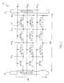
- FIG. 1is a schematic illustration of an EEPROM array of virtual ground NROM memory cells, constructed and operative in accordance with a preferred embodiment of the present invention
- FIGS. 2 and 3are schematic illustrations of the EEPROM array of FIGS. 1 and 2, showing the application of an inhibit voltage during program and erase operations, respectively, in accordance with a preferred embodiment of the present invention.
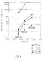
- FIG. 4is a graph illustrating the time required for the threshold voltage to drop by 100 mV as a function of the measured voltage difference between gate and drain voltages applied to the selected cell, for different operating conditions.
- FIG. 1illustrates au EEPROM array 10 constructed and operative in accordance with a preferred embodiment of the present invention.
- Array 10comprises a multiplicity of memory cells 12 each connected to an associated word line, generally designated WL, and two bit lines, generally designated BL.
- memory cells 12are labeled K, P, Q, R, X, Y and Z, respectively.
- memory cells P, Q and Rshare the same word line WL B .
- Cells K, P, X, Q and Yshare the same bit line BL B .
- Cell Zis connected to word line WL C and bit lines BL C and BL D.
- memory cells 12are nitride read only memory (NROM cells.
- NROM cellsare described in various publications, such as U.S. patent applications Ser. Nos. 08/902,890 and 08/905,286, assigned to the common assignee of the present invention, the disclosure of which is incorporated herein by reference.
- U.S. patent application ser. Nos. 08/902,890 and 08/905,286describe, inter alia, the steps of programming reading and erasing NROM cells.
- NROM cellshave not heretofore been used in EEPROM arrays. The present invention enables individually accessing NROM cells in such an EEPROM array, and inhibiting program and erase disturbs in the array.
- NROM cellsmay be single bit. Alternatively, they may have more than one bit wherein two individual bits, a left-side bit 15 and a right-side bit 17 , are stored in physically different areas of the charge-trapping region. Each bit may be single level or multi-level, i.e., may be programed to different voltage levels.
- bit line closest to right-side bit 17e.g., BL B for cell P
- bit line on the other sidee.g., BL A for cell P
- channel hot electronsare used to inject electrons in a lumped pocket close to the drain side of the cell. The electrons are located in localized states in the nitride layer.
- program left-side bit 15 of the cellone simply reverses the role of drain and source during programming.
- a gate voltage V g(typically in the range of approximately 7-10V, e.g., 9V) is applied to word line WL B
- a drain voltage V d(typically in the range of approximately 4-5V, e.g. 4.5V) is applied to bit line BL B
- bit line BL Ais grounded (0V). All other bit lilies are preferably floated near ground prior to any operation (programming or erasing). All other word lines are grounded.
- the right-side bits 17 of unselected cells K and X, and left-side bit 15 of cell Yshare the same bit line BL B as cell P, and also receive drain voltage V d .
- Unselected cell Zdoes not share the same bit line BL B or the same word line WL B as cell P.
- the application of the positive gate voltage to word line WL Bcauses some current flow towards the right side of array 10 , until the bit lines towards the right of bit line BL B attain a drain voltage close to V d .
- This phenomenonis herein referred to as “high voltage propagation”.
- the resultis that both bits of unselected cell Z receive a zero gate voltage and a positive drain voltage, thereby lowering their threshold voltage.
- both the left-side and right-side bits 15is and 17 of cell Z undergo partial erasure.
- right-side bit 17 of cell Yas well as other similarly positioned bits in EEPROM array 10 .
- the duration of programmingis typically in the range of approximately 1-10 ⁇ sec. Since this programming time is relatively short, the right-side bits 17 of cells K and X, and both bits of cells Y and Z are only slightly erased for each programming operation on right-side bit 17 of cell P. The fact that the gate voltage of cells K, X, Y and Z is only zero and not negative, also minimizes the extent of erasure of these bits.
- isolation zones 24In order to contain and control the voltage propagation due to the application of the programming voltage, memory cells 12 are preferably placed between a pair of isolation zones 24 .
- the isolation zones 24define therebetween a slice of word lines and bit lines. There is no voltage propagation past isolation zones 24 .
- the isolation zones 24can divide the array into slices of just one column or a plurality of columns.
- Unselected cells Q and Rshare the same word line WL B as cell P, and also receive the positive gate voltage V g . Therefore, there is virtually no effect on the threshold voltages of both bits of cells Q and R, since tie bit lines on either side of cells Q and R are relatively high.
- bit lines to the left of bit line BL Aare floated near ground, and thus there is virtually no effect on the threshold voltage of the bits of cells on those bit lines.
- Table Asummarizes the disturb on unselected cells due to programming right-side bit 17 of cell P:
- a negative gate voltage V g(such as approximately in the range of ⁇ 5 to ⁇ 7V) is applied to word line WL B
- a positive drain voltage V d(typically in the range of approximately 3-5V, e.g. 4V) is applied to bit line BL B
- bit line BL Ais floating (or driven).
- Left-side bit 15 of cell Qreceives the exact same gate, drain and source voltages. This means that left-side bit 15 of cell Q is also erased together with right-side bit 17 of cell P. Accordingly, after an erasure of right-side bit 17 of cell P, left-side bit 15 of cell Q must be re-programmed to its original value.
- Right-side bit 17 of cell Q and both bits of cell Rshare the same word line WL B as cell P, and also receive the negative gate voltage V g . Since there is only a negative gate voltage applied to word line WL B and the other word lines are grounded, and the bit lines on either side of cells Q and R are floated near ground prior to erasure of right-side bit 17 of cell P, there is no voltage propagation to the other cells and there is negligible erasure of right-side bit 17 of cell Q and both bits of cell R.
- the right-side bits 17 of unselected cells K and X, and left-side bit 15 of cell Yshare the same bit line BL B as cell P, and also receive drain voltage V d . Since the gate voltage of cells K, X and Y is zero, right-side bits 17 of unselected cells K and X, and left-side bit 15 of cell Y experience a lowering of the threshold voltage. In other words, as a consequence of erasing cell P, right-side bits 17 of cells K and X, and left-side bit 15 of cell Y undergo partial erasure. Unfortunately, the duration of erasing is typically in the range of approximately 10 ⁇ sec-10 msec. After many cycles, the accumulated erasure of the unselected cells may be intolerably significant. Unselected cell Z does not share the same bit line BL B or the same word line WL B as cell P, and there is virtually no effect on its threshold voltage. The same holds true for right-side bit 17 of cell Y.
- Table Bsummarizes the disturb effects on unselected cells due to erasing right-side bit 17 of cell P:
- FIG. 2illustrates one example of the invention during programming right-side bit 17 of cell P.
- a gate voltage V g of 9Vis applied to word line WL B
- a drain voltage V d of 4.5Vis applied to bit line BL B
- bit line BL Ais grounded (0V).
- the remaining bit linesare floated near ground before programming.
- a positive gate voltageis applied to word lines WL A (of cell K) and WL C (of cells X and Y).
- the magnitude of the required inhibit voltageis a function of a number of variables, such as, but not limited to programming time, drain voltage applied to the bit line of the programmed cell, voltage difference between gate and drain voltages applied to the programmed cell, and what is considered a tolerable drop in the threshold voltage of the unselected cell.
- the tolerable drop in the threshold voltageis further described hereinbelow with reference to FIG. 4 .
- the inhibit voltageshould be low enough so as not to program unselected bits, and so as not to cause any significant leakage current, but high enough so that the threshold voltages of unselected memory cells are lowered not more than a predetermined amount (over time or after a predetermined amount of operations).
- Row and column decodersmay be used to provide the voltage levels necessary for inhibiting the disturb problem. Such decoders are known in the art and persons skilled in the art may design decoders in accordance with the principles outlined herein.
- an inhibit voltage in the range of 0-2.5Vis typically sufficient to inhibit the partial erasure of unselected cells K, X and Y such that their threshold voltages are lowered by less than 100 mV per 100,000 accesses (which is considered a tolerable lowering of threshold voltage).
- an inhibit voltage of 0-1Vis generally sufficiently low so as not to cause any significant leakage current through the cells that receive this gate voltage.
- Table Csummarizes the effect of the application of the inhibit voltage (e.g., 1V) on the unselected cells when programming right-side bit 17 of cell P:
- FIG. 3illustrates one example of the invention during erasing of right-side bit 17 of cell P.
- a gate voltage V g of ⁇ 7Vis applied to word line WL B
- a drain voltage V d of 4Vis applied to bit line BL B
- the remaining bit linesare floated near ground before erasing.
- a positive gate voltageis applied to word lines WL A (of cell K) and WL C (of cells X and Y).
- an inhibit voltage in the range of 2.54-5V, most preferably in the range of 3-4Vis typically sufficient to inhibit the partial erasure of right-side bits 17 of unselected cells K and X, and left-side bit 15 of cell Y, such that their threshold voltages are lowered by less than about 100 mV per 100,000 accesses
- the application of the inhibit voltage of 3V, for example, to the unselected word linesmay be of sufficient magnitude so as to slightly turn on the cells to the right and left of bit line BL B and cause a voltage propagation to all the bit lines of array 10 , This means that the bit lines towards the right and left of bit line BL B receive a positive voltage, the magnitude of which is a function of the inhibit voltage diminished by the threshold voltage, which in turn depends upon the bulk effect of the memory transistors on those unselected bit lines.
- the bit line voltagesmay rise to about 1.5V.
- the combination of the positive inhibit voltage and the positive drain and source voltagescauses a disturb, but of generally negligible magnitude.
- the combination of the negative gate voltage and the positive drain and source voltagescauses a slight disturb.
- the application of the inhibit voltage on the unselected word lines during an erase operationsignificantly reduces the bit line disturb to the unselected bits, and replaces the relatively high bit line disturb with two other disturbs of a lesser magnitude:
- isolation zones 24reduces the unwanted voltage propagation, and in doing so, prevents the spread of these two minor disturbs.
- Table Dsummarizes the effect of the application of the inhibit voltage (e.g., 3V) on the unselected cells when erasing right-side bit 17 of cell P:
- the magnitude of the requited inhibit voltageis a function of a number of variables, such as, but not limited to, programming time, drain voltage applied to the bit line of the programmed cell, voltage difference between gate and drain voltages applied to the selected cell, and the tolerable drop in the threshold voltage of the unselected cell.
- program disturb of unselected bitsmay also be reduced by using longer programming times and/or lower bit line voltages to complete the programming of the selected bit.
- Erase disturb of unselected bitsmay be reduced by using more negative word line voltages and/or shorter erasing times and/or lower bit line voltages to complete the erasing of the selected bit.
- FIG. 4graphically illustrates the time required for the threshold voltage to drop by 100 mV as a function of the measured voltage difference between gate and drain voltages applied to the selected cell.
- V d /V g V s of 5/0/floatFor a combination of V d /V g V s of 5/0/float, it takes about 20 sec for the threshold voltage to drop by 100 mV. For a combination of V d /V g /V s of 4.5/0/float, it takes about 85 sec for the threshold voltage to drop by 100 mV. Thus, the time for erase disturbs to affect unselected cells is not very prolonged.
- the accumulated disturbi.e., change in threshold voltage, over many access operations, and with the application of the inhibit voltage, may be calculated for the unselected bits as follows, for all operations of erase or program:
- V d /V g /V s4.5/1/4.5 while programming any or all of the other bits on bit lines other than BL B and on word lines other than WL C
- V d /V g /V s1.5/3/1.5 while erasing any or all of the other bits on bit lines other than BL B and on word lines other than WL C , plus
- the accumulated disturb timesare calculated as follows:
- the accumulated disturb timeis:
- ⁇ disturbis the accumulated disturb time
- ⁇ operationis the average time duration of performing operation (erase or program)
- N WLis the number of word lines in the array
- ⁇is the number of times cell is accessed.
- N BLis the number of bit lines in the array.
- the accumulated disturb timeis:
Landscapes
- Engineering & Computer Science (AREA)
- Computer Hardware Design (AREA)
- Microelectronics & Electronic Packaging (AREA)
- Read Only Memory (AREA)
- Non-Volatile Memory (AREA)
- Semiconductor Memories (AREA)
Abstract
Description
| TABLE A | |||||
| Cell | Bit | Vg | Vd | Vs | Effect on Vt |
| P | Right | 9 | 4.5 | 0 | ||
| K | Right | |||||
| 0 | 4.5 | 0 | Partial Erase | |||
| Q | Left | 9 | 4.5 | 4.5 | Virtually None | |
| Q | Right | 9 | 4.5 | 4.5 | Virtually None | |
| R | Both | 9 | 4.5 | 4.5 | Virtually | |
| X | Right | |||||
| 0 | 4.5 | 0 | Partial Erase | |||
| Left | 0 | 4.5 | 4.5 | Partial Erase | ||
| Right | 0 | 4.5 | 4.5 | Partial Erase | ||
| Z | Both | 0 | 4.5 | 4.5 | Partial Erase | |
| TABLE B | |||||||
| Cell | Bit | Vg | Vd | Vs | Effect on Vt | ||
| P | Right | −7 | 4 | Float | Erase | ||
| Right | 0 | 4 | Float | Partial Erase | |||
| Q | Left | −7 | 4 | Float | Erase | ||
| Q | Right | −7 | Float | Float | Virtually None | ||
| R | Both | −7 | Float | Float | Virtually | ||
| X | Right | ||||||
| 0 | 4 | Float | Partial Erase | ||||
| Left | 0 | 4 | Float | Partial Erase | |||
| Y | Right | 0 | Float | Float | Virtually None | ||
| Z | Both | 0 | Float | Float | Virtually None | ||
| TABLE C | |||||
| Cell | Bit | Vg | Vd | Vs | Effect on Vt |
| P | Right | 9 | 4.5 | 0 | ||
| K | Right | |||||
| 1 | 4.5 | 0 | Minute Erase | |||
| Q | Left | 9 | 4.5 | 4.5 | Virtually None | |
| Q | Right | 9 | 4.5 | 4.5 | Virtually None | |
| R | Both | 9 | 4.5 | 4.5 | Virtually | |
| X | Right | |||||
| 1 | 4.5 | 0 | Minute Erase | |||
| Left | 1 | 4.5 | 4.5 | Minute Erase | ||
| Right | 1 | 4.5 | 4.5 | Minute Erase | ||
| Z | Both | 1 | 4.5 | 4.5 | Minute Erase | |
| TABLE D | |||||
| Cell | Bit | Vg | Vd | Vs | Effect on Vt |
| P | Right | −7 | 4 | 1.5 | Erase | |
| Right | 3 | 4 | 1.5 | Virtually None | ||
| Q | Left | −7 | 4 | 1.5 | Erase | |
| Q | Right | −7 | 1.5 | 4 | Minute Erase | |
| R | Both | −7 | 1.5 | 1.5 | Minute Erase | |
| Right | 3 | 4 | 1.5 | Virtually | ||
| Y | Left | |||||
| 3 | 4 | 1.5 | Virtually | |||
| Y | Right | |||||
| 3 | 1.5 | 4 | Virtually None | |||
| Z | Both | 3 | 1.5 | 1.5 | Virtually None | |
Claims (23)
Priority Applications (5)
| Application Number | Priority Date | Filing Date | Title |
|---|---|---|---|
| US09/761,818US6614692B2 (en) | 2001-01-18 | 2001-01-18 | EEPROM array and method for operation thereof |
| IL14765802AIL147658A0 (en) | 2001-01-18 | 2002-01-15 | An eeprom array and method for operation thereof |
| JP2002008945AJP2002279790A (en) | 2001-01-18 | 2002-01-17 | Eeprom array and its operating method |
| EP02250357AEP1227498A3 (en) | 2001-01-18 | 2002-01-18 | An EEPROM array and method for operation thereof |
| US10/155,215US7518908B2 (en) | 2001-01-18 | 2002-05-28 | EEPROM array and method for operation thereof |
Applications Claiming Priority (1)
| Application Number | Priority Date | Filing Date | Title |
|---|---|---|---|
| US09/761,818US6614692B2 (en) | 2001-01-18 | 2001-01-18 | EEPROM array and method for operation thereof |
Related Child Applications (1)
| Application Number | Title | Priority Date | Filing Date |
|---|---|---|---|
| US10/155,215ContinuationUS7518908B2 (en) | 2001-01-18 | 2002-05-28 | EEPROM array and method for operation thereof |
Publications (2)
| Publication Number | Publication Date |
|---|---|
| US20020132436A1 US20020132436A1 (en) | 2002-09-19 |
| US6614692B2true US6614692B2 (en) | 2003-09-02 |
Family
ID=25063339
Family Applications (2)
| Application Number | Title | Priority Date | Filing Date |
|---|---|---|---|
| US09/761,818Expired - LifetimeUS6614692B2 (en) | 2001-01-18 | 2001-01-18 | EEPROM array and method for operation thereof |
| US10/155,215Expired - Fee RelatedUS7518908B2 (en) | 2001-01-18 | 2002-05-28 | EEPROM array and method for operation thereof |
Family Applications After (1)
| Application Number | Title | Priority Date | Filing Date |
|---|---|---|---|
| US10/155,215Expired - Fee RelatedUS7518908B2 (en) | 2001-01-18 | 2002-05-28 | EEPROM array and method for operation thereof |
Country Status (4)
| Country | Link |
|---|---|
| US (2) | US6614692B2 (en) |
| EP (1) | EP1227498A3 (en) |
| JP (1) | JP2002279790A (en) |
| IL (1) | IL147658A0 (en) |
Cited By (33)
| Publication number | Priority date | Publication date | Assignee | Title |
|---|---|---|---|---|
| US20040145024A1 (en)* | 2002-12-31 | 2004-07-29 | En-Hsing Chen | NAND memory array incorporating capacitance boosting of channel regions in unselected memory cells and method for operation of same |
| US20040190341A1 (en)* | 2003-03-24 | 2004-09-30 | Assaf Shappir | Alternating application of pulses on two sides of a cell |
| US20040257880A1 (en)* | 2003-06-17 | 2004-12-23 | Macronix International Co., Ltd. | Overerase protection of memory cells for nonvolatile memory |
| US6917544B2 (en) | 2002-07-10 | 2005-07-12 | Saifun Semiconductors Ltd. | Multiple use memory chip |
| US7221138B2 (en) | 2005-09-27 | 2007-05-22 | Saifun Semiconductors Ltd | Method and apparatus for measuring charge pump output current |
| US7317633B2 (en) | 2004-07-06 | 2008-01-08 | Saifun Semiconductors Ltd | Protection of NROM devices from charge damage |
| US7352627B2 (en) | 2006-01-03 | 2008-04-01 | Saifon Semiconductors Ltd. | Method, system, and circuit for operating a non-volatile memory array |
| US7369440B2 (en) | 2005-01-19 | 2008-05-06 | Saifun Semiconductors Ltd. | Method, circuit and systems for erasing one or more non-volatile memory cells |
| US7405969B2 (en) | 1997-08-01 | 2008-07-29 | Saifun Semiconductors Ltd. | Non-volatile memory cell and non-volatile memory devices |
| US20080198670A1 (en)* | 2004-06-10 | 2008-08-21 | Eduardo Maayan | Reduced power programming of non-volatile cells |
| US20080205140A1 (en)* | 2007-02-26 | 2008-08-28 | Aplus Flash Technology, Inc. | Bit line structure for a multilevel, dual-sided nonvolatile memory cell array |
| US7420848B2 (en) | 2002-01-31 | 2008-09-02 | Saifun Semiconductors Ltd. | Method, system, and circuit for operating a non-volatile memory array |
| US20080225594A1 (en)* | 2007-03-14 | 2008-09-18 | Aplus Flash Technology, Inc. | Bit line gate transistor structure for a multilevel, dual-sided nonvolatile memory cell NAND flash array |
| US7457183B2 (en) | 2003-09-16 | 2008-11-25 | Saifun Semiconductors Ltd. | Operating array cells with matched reference cells |
| US7466594B2 (en) | 2004-08-12 | 2008-12-16 | Saifun Semiconductors Ltd. | Dynamic matching of signal path and reference path for sensing |
| US7512009B2 (en) | 2001-04-05 | 2009-03-31 | Saifun Semiconductors Ltd. | Method for programming a reference cell |
| US7518908B2 (en) | 2001-01-18 | 2009-04-14 | Saifun Semiconductors Ltd. | EEPROM array and method for operation thereof |
| US7532529B2 (en) | 2004-03-29 | 2009-05-12 | Saifun Semiconductors Ltd. | Apparatus and methods for multi-level sensing in a memory array |
| US7535765B2 (en) | 2004-12-09 | 2009-05-19 | Saifun Semiconductors Ltd. | Non-volatile memory device and method for reading cells |
| US7590001B2 (en) | 2007-12-18 | 2009-09-15 | Saifun Semiconductors Ltd. | Flash memory with optimized write sector spares |
| US7605579B2 (en) | 2006-09-18 | 2009-10-20 | Saifun Semiconductors Ltd. | Measuring and controlling current consumption and output current of charge pumps |
| US7638850B2 (en) | 2004-10-14 | 2009-12-29 | Saifun Semiconductors Ltd. | Non-volatile memory structure and method of fabrication |
| US7638835B2 (en) | 2006-02-28 | 2009-12-29 | Saifun Semiconductors Ltd. | Double density NROM with nitride strips (DDNS) |
| US7668017B2 (en) | 2005-08-17 | 2010-02-23 | Saifun Semiconductors Ltd. | Method of erasing non-volatile memory cells |
| US7675782B2 (en) | 2002-10-29 | 2010-03-09 | Saifun Semiconductors Ltd. | Method, system and circuit for programming a non-volatile memory array |
| US7692961B2 (en) | 2006-02-21 | 2010-04-06 | Saifun Semiconductors Ltd. | Method, circuit and device for disturb-control of programming nonvolatile memory cells by hot-hole injection (HHI) and by channel hot-electron (CHE) injection |
| US7701779B2 (en) | 2006-04-27 | 2010-04-20 | Sajfun Semiconductors Ltd. | Method for programming a reference cell |
| US7743230B2 (en) | 2003-01-31 | 2010-06-22 | Saifun Semiconductors Ltd. | Memory array programming circuit and a method for using the circuit |
| US7760554B2 (en) | 2006-02-21 | 2010-07-20 | Saifun Semiconductors Ltd. | NROM non-volatile memory and mode of operation |
| US7786512B2 (en) | 2005-07-18 | 2010-08-31 | Saifun Semiconductors Ltd. | Dense non-volatile memory array and method of fabrication |
| US7808818B2 (en) | 2006-01-12 | 2010-10-05 | Saifun Semiconductors Ltd. | Secondary injection for NROM |
| US8053812B2 (en) | 2005-03-17 | 2011-11-08 | Spansion Israel Ltd | Contact in planar NROM technology |
| US8253452B2 (en) | 2006-02-21 | 2012-08-28 | Spansion Israel Ltd | Circuit and method for powering up an integrated circuit and an integrated circuit utilizing same |
Families Citing this family (25)
| Publication number | Priority date | Publication date | Assignee | Title |
|---|---|---|---|---|
| IL125604A (en) | 1997-07-30 | 2004-03-28 | Saifun Semiconductors Ltd | Non-volatile electrically erasable and programmble semiconductor memory cell utilizing asymmetrical charge |
| US6928001B2 (en) | 2000-12-07 | 2005-08-09 | Saifun Semiconductors Ltd. | Programming and erasing methods for a non-volatile memory cell |
| US6396741B1 (en) | 2000-05-04 | 2002-05-28 | Saifun Semiconductors Ltd. | Programming of nonvolatile memory cells |
| US6643181B2 (en) | 2001-10-24 | 2003-11-04 | Saifun Semiconductors Ltd. | Method for erasing a memory cell |
| US6975536B2 (en) | 2002-01-31 | 2005-12-13 | Saifun Semiconductors Ltd. | Mass storage array and methods for operation thereof |
| US7190620B2 (en)* | 2002-01-31 | 2007-03-13 | Saifun Semiconductors Ltd. | Method for operating a memory device |
| DE60212938D1 (en)* | 2002-04-30 | 2006-08-17 | St Microelectronics Srl | Method for reducing unwanted deletion when programming a nonvolatile NROM |
| US6826107B2 (en) | 2002-08-01 | 2004-11-30 | Saifun Semiconductors Ltd. | High voltage insertion in flash memory cards |
| US6992932B2 (en) | 2002-10-29 | 2006-01-31 | Saifun Semiconductors Ltd | Method circuit and system for read error detection in a non-volatile memory array |
| US6963505B2 (en) | 2002-10-29 | 2005-11-08 | Aifun Semiconductors Ltd. | Method circuit and system for determining a reference voltage |
| US6906959B2 (en)* | 2002-11-27 | 2005-06-14 | Advanced Micro Devices, Inc. | Method and system for erasing a nitride memory device |
| US6967896B2 (en) | 2003-01-30 | 2005-11-22 | Saifun Semiconductors Ltd | Address scramble |
| US7085170B2 (en)* | 2003-08-07 | 2006-08-01 | Micron Technology, Ind. | Method for erasing an NROM cell |
| US6914819B2 (en)* | 2003-09-04 | 2005-07-05 | Macronix International Co., Ltd. | Non-volatile flash memory |
| US6954393B2 (en)* | 2003-09-16 | 2005-10-11 | Saifun Semiconductors Ltd. | Reading array cell with matched reference cell |
| WO2005094178A2 (en) | 2004-04-01 | 2005-10-13 | Saifun Semiconductors Ltd. | Method, circuit and systems for erasing one or more non-volatile memory cells |
| US7755938B2 (en) | 2004-04-19 | 2010-07-13 | Saifun Semiconductors Ltd. | Method for reading a memory array with neighbor effect cancellation |
| DE112004002851B4 (en)* | 2004-05-11 | 2023-05-25 | Spansion Llc (N.D.Ges.D. Staates Delaware) | Semiconductor device and programming method |
| US7257025B2 (en)* | 2004-12-09 | 2007-08-14 | Saifun Semiconductors Ltd | Method for reading non-volatile memory cells |
| US8400841B2 (en) | 2005-06-15 | 2013-03-19 | Spansion Israel Ltd. | Device to program adjacent storage cells of different NROM cells |
| US7184313B2 (en) | 2005-06-17 | 2007-02-27 | Saifun Semiconductors Ltd. | Method circuit and system for compensating for temperature induced margin loss in non-volatile memory cells |
| US8116142B2 (en)* | 2005-09-06 | 2012-02-14 | Infineon Technologies Ag | Method and circuit for erasing a non-volatile memory cell |
| KR101608339B1 (en)* | 2009-06-08 | 2016-04-11 | 삼성전자주식회사 | Method and device for measuring location, and moving object |
| US8471328B2 (en) | 2010-07-26 | 2013-06-25 | United Microelectronics Corp. | Non-volatile memory and manufacturing method thereof |
| US20120140556A1 (en)* | 2010-12-07 | 2012-06-07 | Macronix International Co., Ltd. | Method of operating flash memory |
Citations (113)
| Publication number | Priority date | Publication date | Assignee | Title |
|---|---|---|---|---|
| US3895360A (en) | 1974-01-29 | 1975-07-15 | Westinghouse Electric Corp | Block oriented random access memory |
| US4016588A (en) | 1974-12-27 | 1977-04-05 | Nippon Electric Company, Ltd. | Non-volatile semiconductor memory device |
| US4017888A (en) | 1975-12-31 | 1977-04-12 | International Business Machines Corporation | Non-volatile metal nitride oxide semiconductor device |
| US4151021A (en) | 1977-01-26 | 1979-04-24 | Texas Instruments Incorporated | Method of making a high density floating gate electrically programmable ROM |
| US4173766A (en) | 1977-09-16 | 1979-11-06 | Fairchild Camera And Instrument Corporation | Insulated gate field-effect transistor read-only memory cell |
| US4173791A (en) | 1977-09-16 | 1979-11-06 | Fairchild Camera And Instrument Corporation | Insulated gate field-effect transistor read-only memory array |
| US4281397A (en) | 1979-10-29 | 1981-07-28 | Texas Instruments Incorporated | Virtual ground MOS EPROM or ROM matrix |
| US4306353A (en) | 1979-06-13 | 1981-12-22 | Siemens Aktiengesellschaft | Process for production of integrated MOS circuits with and without MNOS memory transistors in silicon-gate technology |
| US4342149A (en) | 1979-11-23 | 1982-08-03 | Siemens Aktiengesellschaft | Method of making very short channel length MNOS and MOS devices by double implantation of one conductivity type subsequent to other type implantation |
| US4360900A (en) | 1978-11-27 | 1982-11-23 | Texas Instruments Incorporated | Non-volatile semiconductor memory elements |
| US4380057A (en) | 1980-10-27 | 1983-04-12 | International Business Machines Corporation | Electrically alterable double dense memory |
| US4388705A (en) | 1981-10-01 | 1983-06-14 | Mostek Corporation | Semiconductor memory circuit |
| US4389705A (en) | 1981-08-21 | 1983-06-21 | Mostek Corporation | Semiconductor memory circuit with depletion data transfer transistor |
| US4471373A (en) | 1980-02-27 | 1984-09-11 | Hitachi, Ltd. | Semiconductor integrated circuit device with memory MISFETS and thin and thick gate insulator MISFETS |
| US4527257A (en) | 1982-08-25 | 1985-07-02 | Westinghouse Electric Corp. | Common memory gate non-volatile transistor memory |
| GB2157489A (en) | 1984-03-23 | 1985-10-23 | Hitachi Ltd | A semiconductor integrated circuit memory device |
| US4586163A (en) | 1982-09-13 | 1986-04-29 | Toshiba Shibaura Denki Kabushiki Kaisha | Multi-bit-per-cell read only memory circuit |
| US4630085A (en) | 1984-02-28 | 1986-12-16 | Nec Corporation | Erasable, programmable read-only memory device |
| US4667217A (en) | 1985-04-19 | 1987-05-19 | Ncr Corporation | Two bit vertically/horizontally integrated memory cell |
| US4780424A (en) | 1987-09-28 | 1988-10-25 | Intel Corporation | Process for fabricating electrically alterable floating gate memory devices |
| US4847808A (en) | 1986-04-22 | 1989-07-11 | Nec Corporation | Read only semiconductor memory having multiple bit cells |
| US4870470A (en) | 1987-10-16 | 1989-09-26 | International Business Machines Corporation | Non-volatile memory cell having Si rich silicon nitride charge trapping layer |
| US4916671A (en) | 1988-09-06 | 1990-04-10 | Mitsubishi Denki Kabushiki Kaisha | Semiconductor memory device having sense amplifier having improved activation timing thereof and operating method thereof |
| US4941028A (en) | 1988-08-10 | 1990-07-10 | Actel Corporation | Structure for protecting thin dielectrics during processing |
| US5021999A (en) | 1987-12-17 | 1991-06-04 | Mitsubishi Denki Kabushiki Kaisha | Non-volatile semiconductor memory device with facility of storing tri-level data |
| US5075245A (en) | 1990-08-03 | 1991-12-24 | Intel Corporation | Method for improving erase characteristics of buried bit line flash EPROM devices without using sacrificial oxide growth and removal steps |
| US5117389A (en) | 1990-09-05 | 1992-05-26 | Macronix International Co., Ltd. | Flat-cell read-only-memory integrated circuit |
| US5168334A (en) | 1987-07-31 | 1992-12-01 | Texas Instruments, Incorporated | Non-volatile semiconductor memory |
| US5172338A (en) | 1989-04-13 | 1992-12-15 | Sundisk Corporation | Multi-state EEprom read and write circuits and techniques |
| US5175120A (en) | 1991-10-11 | 1992-12-29 | Micron Technology, Inc. | Method of processing a semiconductor wafer to form an array of nonvolatile memory devices employing floating gate transistors and peripheral area having CMOS transistors |
| US5204835A (en) | 1990-06-13 | 1993-04-20 | Waferscale Integration Inc. | Eprom virtual ground array |
| US5214303A (en) | 1991-02-08 | 1993-05-25 | Sharp Kabushiki Kaisha | Semiconductor device ROM having an offset region |
| US5241497A (en) | 1990-06-14 | 1993-08-31 | Creative Integrated Systems, Inc. | VLSI memory with increased memory access speed, increased memory cell density and decreased parasitic capacitance |
| US5260593A (en) | 1991-12-10 | 1993-11-09 | Micron Technology, Inc. | Semiconductor floating gate device having improved channel-floating gate interaction |
| US5268861A (en) | 1991-04-10 | 1993-12-07 | Sharp Kabushiki Kaisha | Semiconductor read only memory |
| US5289412A (en) | 1992-06-19 | 1994-02-22 | Intel Corporation | High-speed bias-stabilized current-mirror referencing circuit for non-volatile memories |
| US5293563A (en) | 1988-12-29 | 1994-03-08 | Sharp Kabushiki Kaisha | Multi-level memory cell with increased read-out margin |
| US5305262A (en) | 1991-09-11 | 1994-04-19 | Kawasaki Steel Corporation | Semiconductor integrated circuit |
| US5311049A (en) | 1991-10-17 | 1994-05-10 | Rohm Co., Ltd. | Non-volatile semiconductor memory with outer drain diffusion layer |
| US5315541A (en) | 1992-07-24 | 1994-05-24 | Sundisk Corporation | Segmented column memory array |
| US5345425A (en) | 1990-11-20 | 1994-09-06 | Fujitsu Limited | Semiconductor memory device |
| US5349221A (en) | 1991-10-25 | 1994-09-20 | Rohm Co., Ltd. | Semiconductor memory device and method of reading out information for the same |
| US5350710A (en) | 1993-06-24 | 1994-09-27 | United Microelectronics Corporation | Device for preventing antenna effect on circuit |
| US5359554A (en) | 1991-08-27 | 1994-10-25 | Matsushita Electric Industrial Co., Ltd. | Semiconductor memory device having an energy gap for high speed operation |
| US5393701A (en) | 1993-04-08 | 1995-02-28 | United Microelectronics Corporation | Layout design to eliminate process antenna effect |
| US5394355A (en) | 1990-08-28 | 1995-02-28 | Mitsubishi Denki Kabushiki Kaisha | Read only memory for storing multi-data |
| US5399891A (en) | 1992-01-22 | 1995-03-21 | Macronix International Co., Ltd. | Floating gate or flash EPROM transistor array having contactless source and drain diffusions |
| US5412601A (en) | 1992-08-31 | 1995-05-02 | Nippon Steel Corporation | Non-volatile semiconductor memory device capable of storing multi-value data in each memory cell |
| US5414693A (en) | 1991-08-29 | 1995-05-09 | Hyundai Electronics Industries Co., Ltd. | Self-aligned dual-bit split gate (DSG) flash EEPROM cell |
| US5418176A (en) | 1994-02-17 | 1995-05-23 | United Microelectronics Corporation | Process for producing memory devices having narrow buried N+ lines |
| US5418743A (en) | 1992-12-07 | 1995-05-23 | Nippon Steel Corporation | Method of writing into non-volatile semiconductor memory |
| US5422844A (en) | 1992-12-21 | 1995-06-06 | National Semiconductor Corporation | Memory array with field oxide islands eliminated and method |
| US5424978A (en) | 1993-03-15 | 1995-06-13 | Nippon Steel Corporation | Non-volatile semiconductor memory cell capable of storing more than two different data and method of using the same |
| US5426605A (en) | 1992-08-19 | 1995-06-20 | U.S. Philips Corporation | Semiconductor memory device |
| US5434825A (en) | 1988-06-08 | 1995-07-18 | Harari; Eliyahou | Flash EEPROM system cell array with more than two storage states per memory cell |
| US5450341A (en) | 1992-08-31 | 1995-09-12 | Nippon Steel Corporation | Non-volatile semiconductor memory device having memory cells, each for at least three different data writable thereinto selectively and a method of using the same |
| US5450354A (en) | 1992-08-31 | 1995-09-12 | Nippon Steel Corporation | Non-volatile semiconductor memory device detachable deterioration of memory cells |
| US5467308A (en) | 1994-04-05 | 1995-11-14 | Motorola Inc. | Cross-point eeprom memory array |
| US5477499A (en) | 1993-10-13 | 1995-12-19 | Advanced Micro Devices, Inc. | Memory architecture for a three volt flash EEPROM |
| US5495440A (en) | 1993-01-19 | 1996-02-27 | Mitsubishi Denki Kabushiki Kaisha | Semiconductor memory device having hierarchical bit line structure |
| US5496753A (en) | 1992-05-29 | 1996-03-05 | Citizen Watch, Co., Ltd. | Method of fabricating a semiconductor nonvolatile storage device |
| US5521870A (en) | 1993-12-07 | 1996-05-28 | Nec Corporation | Semiconductor memory device having a coincidence detection circuit and its test method |
| US5523251A (en) | 1994-10-05 | 1996-06-04 | United Microelectronics Corp. | Method for fabricating a self aligned mask ROM |
| US5553018A (en) | 1995-06-07 | 1996-09-03 | Advanced Micro Devices, Inc. | Nonvolatile memory cell formed using self aligned source implant |
| US5583808A (en) | 1994-09-16 | 1996-12-10 | National Semiconductor Corporation | EPROM array segmented for high performance and method for controlling same |
| US5599727A (en) | 1994-12-15 | 1997-02-04 | Sharp Kabushiki Kaisha | Method for producing a floating gate memory device including implanting ions through an oxidized portion of the silicon film from which the floating gate is formed |
| US5623438A (en) | 1992-11-30 | 1997-04-22 | Sgs-Thomson Microelectronics, Inc. | Virtual ground read only memory circuit |
| US5654568A (en) | 1992-01-17 | 1997-08-05 | Rohm Co., Ltd. | Semiconductor device including nonvolatile memories |
| US5661060A (en) | 1994-12-28 | 1997-08-26 | National Semiconductor Corporation | Method for forming field oxide regions |
| US5683925A (en) | 1996-06-13 | 1997-11-04 | Waferscale Integration Inc. | Manufacturing method for ROM array with minimal band-to-band tunneling |
| US5712814A (en) | 1994-07-18 | 1998-01-27 | Sgs-Thomson Microelectronics S.R.L. | Nonvolatile memory cell and a method for forming the same |
| US5726946A (en) | 1994-06-02 | 1998-03-10 | Mitsubishi Denki Kabushiki Kaisha | Semiconductor integrated circuit device having hierarchical power source arrangement |
| US5751037A (en) | 1995-07-27 | 1998-05-12 | Sony Corporation | Non-volatile memory cell having dual gate electrodes |
| US5754475A (en) | 1996-06-24 | 1998-05-19 | Advanced Micro Devices, Inc. | Bit line discharge method for reading a multiple bits-per-cell flash EEPROM |
| US5768192A (en)* | 1996-07-23 | 1998-06-16 | Saifun Semiconductors, Ltd. | Non-volatile semiconductor memory cell utilizing asymmetrical charge trapping |
| US5777919A (en) | 1996-09-13 | 1998-07-07 | Holtek Microelectronics, Inc. | Select gate enhanced high density read-only-memory device |
| US5787036A (en) | 1995-12-12 | 1998-07-28 | Nec Corporation | Flash memory including improved transistor cells and a method of programming the memory |
| US5793079A (en) | 1996-07-22 | 1998-08-11 | Catalyst Semiconductor, Inc. | Single transistor non-volatile electrically alterable semiconductor memory device |
| US5834851A (en) | 1990-02-09 | 1998-11-10 | Hitachi, Ltd. | SRAM having load transistor formed above driver transistor |
| US5836772A (en) | 1994-09-29 | 1998-11-17 | Macronix International Co., Ltd. | Interpoly dielectric process |
| US5841700A (en) | 1992-09-08 | 1998-11-24 | National Semiconductor Corporation | Source-coupling, split gate, virtual ground flash EEPROM array |
| US5847441A (en) | 1996-05-10 | 1998-12-08 | Micron Technology, Inc. | Semiconductor junction antifuse circuit |
| US5862076A (en) | 1990-11-13 | 1999-01-19 | Waferscale Integration, Inc. | Fast EPROM array |
| US5864164A (en) | 1996-12-09 | 1999-01-26 | United Microelectronics Corp. | Multi-stage ROM structure and method for fabricating the same |
| US5870335A (en) | 1997-03-06 | 1999-02-09 | Agate Semiconductor, Inc. | Precision programming of nonvolatile memory cells |
| US5946558A (en) | 1997-02-05 | 1999-08-31 | United Microelectronics Corp. | Method of making ROM components |
| US5949728A (en) | 1997-12-12 | 1999-09-07 | Scenix Semiconductor, Inc. | High speed, noise immune, single ended sensing scheme for non-volatile memories |
| US5963412A (en) | 1997-11-13 | 1999-10-05 | Advanced Micro Devices, Inc. | Process induced charging damage control device |
| US5963465A (en) | 1997-12-12 | 1999-10-05 | Saifun Semiconductors, Ltd. | Symmetric segmented memory array architecture |
| US5966603A (en) | 1997-06-11 | 1999-10-12 | Saifun Semiconductors Ltd. | NROM fabrication method with a periphery portion |
| US5973373A (en) | 1994-09-28 | 1999-10-26 | Siemens Aktiengesellschaft | Read-only-memory cell arrangement using vertical MOS transistors and gate dielectrics of different thicknesses and method for its production |
| US5991202A (en) | 1998-09-24 | 1999-11-23 | Advanced Micro Devices, Inc. | Method for reducing program disturb during self-boosting in a NAND flash memory |
| US5990526A (en) | 1997-02-20 | 1999-11-23 | Stmicroelectronics S.R.L. | Memory device with a cell array in triple well, and related manufacturing process |
| US5999444A (en)* | 1997-09-02 | 1999-12-07 | Sony Corporation | Nonvolatile semiconductor memory device and writing and erasing method of the same |
| US6011725A (en)* | 1997-08-01 | 2000-01-04 | Saifun Semiconductors, Ltd. | Two bit non-volatile electrically erasable and programmable semiconductor memory cell utilizing asymmetrical charge trapping |
| US6018186A (en) | 1997-04-15 | 2000-01-25 | United Microelectronics Corp. | Three-dimensional, deep-trench, high-density read-only memory (ROM) and its manufacturing method |
| US6020241A (en) | 1997-12-22 | 2000-02-01 | Taiwan Semiconductor Manufacturing Company | Post metal code engineering for a ROM |
| US6028324A (en) | 1997-03-07 | 2000-02-22 | Taiwan Semiconductor Manufacturing Company | Test structures for monitoring gate oxide defect densities and the plasma antenna effect |
| US6030871A (en) | 1998-05-05 | 2000-02-29 | Saifun Semiconductors Ltd. | Process for producing two bit ROM cell utilizing angled implant |
| US6034403A (en) | 1998-06-25 | 2000-03-07 | Acer Semiconductor Manufacturing, Inc. | High density flat cell mask ROM |
| US6063666A (en) | 1998-06-16 | 2000-05-16 | Advanced Micro Devices, Inc. | RTCVD oxide and N2 O anneal for top oxide of ONO film |
| US6081456A (en)* | 1999-02-04 | 2000-06-27 | Tower Semiconductor Ltd. | Bit line control circuit for a memory array using 2-bit non-volatile memory cells |
| US6128226A (en) | 1999-02-04 | 2000-10-03 | Saifun Semiconductors Ltd. | Method and apparatus for operating with a close to ground signal |
| US6134156A (en) | 1999-02-04 | 2000-10-17 | Saifun Semiconductors Ltd. | Method for initiating a retrieval procedure in virtual ground arrays |
| US6137718A (en) | 1996-08-01 | 2000-10-24 | Siemens Aktiengesellschaft | Method for operating a non-volatile memory cell arrangement |
| US6147904A (en)* | 1999-02-04 | 2000-11-14 | Tower Semiconductor Ltd. | Redundancy method and structure for 2-bit non-volatile memory cells |
| US6163048A (en)* | 1995-10-25 | 2000-12-19 | Cypress Semiconductor Corporation | Semiconductor non-volatile memory device having a NAND cell structure |
| EP1073120A2 (en) | 1999-07-30 | 2001-01-31 | Saifun Semiconductors Ltd | An NROM fabrication method |
| US6218695B1 (en)* | 1999-06-28 | 2001-04-17 | Tower Semiconductor Ltd. | Area efficient column select circuitry for 2-bit non-volatile memory cells |
| US6222768B1 (en)* | 2000-01-28 | 2001-04-24 | Advanced Micro Devices, Inc. | Auto adjusting window placement scheme for an NROM virtual ground array |
| US6256231B1 (en) | 1999-02-04 | 2001-07-03 | Tower Semiconductor Ltd. | EEPROM array using 2-bit non-volatile memory cells and method of implementing same |
| EP0693781B1 (en) | 1994-07-13 | 2002-10-02 | United Microelectronics Corporation | Grounding method for eliminating process antenna effect |
| EP0751560B1 (en) | 1995-06-30 | 2002-11-27 | STMicroelectronics S.r.l. | Process for forming an integrated circuit comprising non-volatile memory cells and side transistors of at least two different types, and corresponding IC |
Family Cites Families (214)
| Publication number | Priority date | Publication date | Assignee | Title |
|---|---|---|---|---|
| US537134A (en)* | 1895-04-09 | Haeey toechiani | ||
| US14290A (en)* | 1856-02-19 | Michael phelan | ||
| US27858A (en)* | 1860-04-10 | Edmund b | ||
| US34397A (en)* | 1862-02-11 | Improvement in spool-holding devices | ||
| US214844A (en)* | 1879-04-29 | Improvement in wind-engines | ||
| US190786A (en)* | 1877-05-15 | Improvement in finishing woven fabrics | ||
| US64911A (en)* | 1867-05-21 | Charles a | ||
| US751560A (en)* | 1904-02-09 | Stocking-top-cutting machine | ||
| US693781A (en)* | 1901-09-10 | 1902-02-18 | Joel H Brown | Dust-guard for hose-couplings. |
| US1297899A (en)* | 1916-06-26 | 1919-03-18 | Dennis Parks | Machine for cutting blanks from leather. |
| GB1297899A (en) | 1970-10-02 | 1972-11-29 | ||
| GB1392599A (en)* | 1971-07-28 | 1975-04-30 | Mullard Ltd | Semiconductor memory elements |
| US3881180A (en)* | 1971-11-30 | 1975-04-29 | Texas Instruments Inc | Non-volatile memory cell |
| US4145703A (en)* | 1977-04-15 | 1979-03-20 | Supertex, Inc. | High power MOS device and fabrication method therefor |
| US4373248A (en)* | 1978-07-12 | 1983-02-15 | Texas Instruments Incorporated | Method of making high density semiconductor device such as floating gate electrically programmable ROM or the like |
| DE2832388C2 (en)* | 1978-07-24 | 1986-08-14 | Siemens Ag, 1000 Berlin Und 8000 Muenchen | Process for the production of MNOS and MOS transistors in silicon gate technology on a semiconductor substrate |
| US4247861A (en)* | 1979-03-09 | 1981-01-27 | Rca Corporation | High performance electrically alterable read-only memory (EAROM) |
| WO1981000790A1 (en) | 1979-09-13 | 1981-03-19 | Ncr Co | Silicon gate non-volatile memory device |
| JPS5656677A (en)* | 1979-10-13 | 1981-05-18 | Toshiba Corp | Semiconductor memory device |
| US4342102A (en) | 1980-06-18 | 1982-07-27 | Signetics Corporation | Semiconductor memory array |
| US4521796A (en) | 1980-12-11 | 1985-06-04 | General Instrument Corporation | Memory implant profile for improved channel shielding in electrically alterable read only memory semiconductor device |
| EP0056195B1 (en) | 1980-12-25 | 1986-06-18 | Fujitsu Limited | Nonvolatile semiconductor memory device |
| US4448400A (en) | 1981-07-13 | 1984-05-15 | Eliyahou Harari | Highly scalable dynamic RAM cell with self-signal amplification |
| US4435786A (en)* | 1981-11-23 | 1984-03-06 | Fairchild Camera And Instrument Corporation | Self-refreshing memory cell |
| US4494016A (en)* | 1982-07-26 | 1985-01-15 | Sperry Corporation | High performance MESFET transistor for VLSI implementation |
| US4613956A (en) | 1983-02-23 | 1986-09-23 | Texas Instruments Incorporated | Floating gate memory with improved dielectric |
| US4769340A (en) | 1983-11-28 | 1988-09-06 | Exel Microelectronics, Inc. | Method for making electrically programmable memory device by doping the floating gate by implant |
| US5352620A (en) | 1984-05-23 | 1994-10-04 | Hitachi, Ltd. | Method of making semiconductor device with memory cells and peripheral transistors |
| US4663645A (en) | 1984-05-23 | 1987-05-05 | Hitachi, Ltd. | Semiconductor device of an LDD structure having a floating gate |
| US4665426A (en) | 1985-02-01 | 1987-05-12 | Advanced Micro Devices, Inc. | EPROM with ultraviolet radiation transparent silicon nitride passivation layer |
| US4742491A (en) | 1985-09-26 | 1988-05-03 | Advanced Micro Devices, Inc. | Memory cell having hot-hole injection erase mode |
| US4760555A (en) | 1986-04-21 | 1988-07-26 | Texas Instruments Incorporated | Memory array with an array reorganizer |
| JPH0521758Y2 (en) | 1986-05-19 | 1993-06-03 | ||
| US4758869A (en) | 1986-08-29 | 1988-07-19 | Waferscale Integration, Inc. | Nonvolatile floating gate transistor structure |
| EP0283436B1 (en)* | 1987-03-13 | 1991-01-16 | Ciba-Geigy Ag | Perylene-tetracarboxylic-acid diimides with long-chain residue containing carbonyl groups |
| US4839705A (en) | 1987-12-16 | 1989-06-13 | Texas Instruments Incorporated | X-cell EEPROM array |
| US5159570A (en) | 1987-12-22 | 1992-10-27 | Texas Instruments Incorporated | Four memory state EEPROM |
| US5042009A (en) | 1988-12-09 | 1991-08-20 | Waferscale Integration, Inc. | Method for programming a floating gate memory device |
| US5120672A (en) | 1989-02-22 | 1992-06-09 | Texas Instruments Incorporated | Fabricating a single level merged EEPROM cell having an ONO memory stack substantially spaced from the source region |
| EP0935255A2 (en) | 1989-04-13 | 1999-08-11 | SanDisk Corporation | Flash EEPROM system |
| US5104819A (en)* | 1989-08-07 | 1992-04-14 | Intel Corporation | Fabrication of interpoly dielctric for EPROM-related technologies |
| US5027321A (en) | 1989-11-21 | 1991-06-25 | Intel Corporation | Apparatus and method for improved reading/programming of virtual ground EPROM arrays |
| US4992391A (en)* | 1989-11-29 | 1991-02-12 | Advanced Micro Devices, Inc. | Process for fabricating a control gate for a floating gate FET |
| JPH04226071A (en) | 1990-05-16 | 1992-08-14 | Ricoh Co Ltd | Semiconductor memory device |
| US5086325A (en)* | 1990-11-21 | 1992-02-04 | Atmel Corporation | Narrow width EEPROM with single diffusion electrode formation |
| US5094968A (en)* | 1990-11-21 | 1992-03-10 | Atmel Corporation | Fabricating a narrow width EEPROM with single diffusion electrode formation |
| JPH04291962A (en) | 1991-03-20 | 1992-10-16 | Fujitsu Ltd | Mask ROM manufacturing method and mask ROM |
| US5424567A (en) | 1991-05-15 | 1995-06-13 | North American Philips Corporation | Protected programmable transistor with reduced parasitic capacitances and method of fabrication |
| US5338954A (en) | 1991-10-31 | 1994-08-16 | Rohm Co., Ltd. | Semiconductor memory device having an insulating film and a trap film joined in a channel region |
| US5357134A (en) | 1991-10-31 | 1994-10-18 | Rohm Co., Ltd. | Nonvolatile semiconductor device having charge trap film containing silicon crystal grains |
| JPH05129284A (en) | 1991-11-06 | 1993-05-25 | Sony Corp | Plasma SiN film forming condition setting method and semiconductor device manufacturing method |
| JP3103637B2 (en) | 1991-11-28 | 2000-10-30 | 株式会社メガチップス | Semiconductor storage device |
| US6222762B1 (en) | 1992-01-14 | 2001-04-24 | Sandisk Corporation | Multi-state memory |
| US5293328A (en) | 1992-01-15 | 1994-03-08 | National Semiconductor Corporation | Electrically reprogrammable EPROM cell with merged transistor and optiumum area |
| US5324675A (en) | 1992-03-31 | 1994-06-28 | Kawasaki Steel Corporation | Method of producing semiconductor devices of a MONOS type |
| JPH05290584A (en)* | 1992-04-08 | 1993-11-05 | Nec Corp | Semiconductor memory |
| JPH065823A (en) | 1992-06-19 | 1994-01-14 | Toshiba Corp | Nonvolatile semiconductor memory device and method of using the same |
| JP3036565B2 (en) | 1992-08-28 | 2000-04-24 | 日本電気株式会社 | Manufacturing method of nonvolatile semiconductor memory device |
| US5436481A (en) | 1993-01-21 | 1995-07-25 | Nippon Steel Corporation | MOS-type semiconductor device and method of making the same |
| KR100299879B1 (en) | 1993-02-01 | 2001-10-22 | 클라크 3세 존 엠. | Ultra-high density alternating metal virtual ground ROM |
| DE9305576U1 (en) | 1993-04-14 | 1993-07-08 | Holzrichter, Dieter, Dr.med., 2000 Hamburg | Data recording device |
| JP3317459B2 (en)* | 1993-04-30 | 2002-08-26 | ローム株式会社 | Nonvolatile storage element, nonvolatile storage device using the same, method of driving this storage device, and method of manufacturing this storage element |
| US5335198A (en) | 1993-05-06 | 1994-08-02 | Advanced Micro Devices, Inc. | Flash EEPROM array with high endurance |
| FR2705686B1 (en) | 1993-05-28 | 1995-08-18 | Transgene Sa | New defective adenoviruses and corresponding complementation lines. |
| JP3554572B2 (en) | 1993-06-11 | 2004-08-18 | 株式会社ルネサステクノロジ | Non-volatile semiconductor circuit |
| US5400286A (en)* | 1993-08-17 | 1995-03-21 | Catalyst Semiconductor Corp. | Self-recovering erase scheme to enhance flash memory endurance |
| JP3463030B2 (en) | 1993-08-27 | 2003-11-05 | 株式会社東芝 | Nonvolatile semiconductor memory device |
| US5563823A (en) | 1993-08-31 | 1996-10-08 | Macronix International Co., Ltd. | Fast FLASH EPROM programming and pre-programming circuit design |
| US5828601A (en) | 1993-12-01 | 1998-10-27 | Advanced Micro Devices, Inc. | Programmed reference |
| JPH07193151A (en) | 1993-12-27 | 1995-07-28 | Toshiba Corp | Nonvolatile semiconductor memory device and its storage method |
| US5440505A (en) | 1994-01-21 | 1995-08-08 | Intel Corporation | Method and circuitry for storing discrete amounts of charge in a single memory element |
| FR2715758B1 (en)* | 1994-01-31 | 1996-03-22 | Sgs Thomson Microelectronics | Source-programmable, non-volatile flip-flop, especially for memory redundancy circuits. |
| FR2715782B1 (en)* | 1994-01-31 | 1996-03-22 | Sgs Thomson Microelectronics | Programmable non-volatile bistable flip-flop, with predefined initial state, in particular for memory redundancy circuit. |
| JP3397427B2 (en) | 1994-02-02 | 2003-04-14 | 株式会社東芝 | Semiconductor storage device |
| JP3584338B2 (en) | 1994-03-03 | 2004-11-04 | ローム・ユーエスエー・インク | Method for erasing electrically erasable and programmable devices |
| US5523972A (en) | 1994-06-02 | 1996-06-04 | Intel Corporation | Method and apparatus for verifying the programming of multi-level flash EEPROM memory |
| KR100372905B1 (en) | 1994-09-13 | 2003-05-01 | 애질런트 테크놀로지스, 인크. | A device and method of manufacture for frotection against plasma charging damage in advanced mos technologies |
| JP3730272B2 (en) | 1994-09-17 | 2005-12-21 | 株式会社東芝 | Nonvolatile semiconductor memory device |
| WO1996015553A1 (en) | 1994-11-15 | 1996-05-23 | Advanced Micro Devices, Inc. | Transistor structure with specific gate and pad areas |
| JPH08153396A (en) | 1994-11-28 | 1996-06-11 | Sony Corp | Semiconductor nonvolatile memory |
| US5537358A (en) | 1994-12-06 | 1996-07-16 | National Semiconductor Corporation | Flash memory having adaptive sensing and method |
| DE19505293A1 (en) | 1995-02-16 | 1996-08-22 | Siemens Ag | Multi-value read-only memory cell with improved signal-to-noise ratio |
| US5801076A (en) | 1995-02-21 | 1998-09-01 | Advanced Micro Devices, Inc. | Method of making non-volatile memory device having a floating gate with enhanced charge retention |
| US5518942A (en) | 1995-02-22 | 1996-05-21 | Alliance Semiconductor Corporation | Method of making flash EPROM cell having improved erase characteristics by using a tilt angle implant |
| US6353554B1 (en)* | 1995-02-27 | 2002-03-05 | Btg International Inc. | Memory apparatus including programmable non-volatile multi-bit memory cell, and apparatus and method for demarcating memory states of the cell |
| US5617357A (en)* | 1995-04-07 | 1997-04-01 | Advanced Micro Devices, Inc. | Flash EEPROM memory with improved discharge speed using substrate bias and method therefor |
| KR100187656B1 (en) | 1995-05-16 | 1999-06-01 | 김주용 | Method for manufacturing a flash eeprom and the programming method |
| US6034896A (en)* | 1995-07-03 | 2000-03-07 | The University Of Toronto, Innovations Foundation | Method of fabricating a fast programmable flash E2 PROM cell |
| EP0753859B1 (en) | 1995-07-14 | 2000-01-26 | STMicroelectronics S.r.l. | Method for setting the threshold voltage of a reference memory cell |
| JPH09115291A (en) | 1995-10-17 | 1997-05-02 | Sony Corp | Semiconductor nonvolatile memory and its write method |
| JPH09153559A (en) | 1995-12-01 | 1997-06-10 | Hitachi Ltd | Semiconductor integrated circuit device, operating method thereof, and electronic circuit device |
| JP3251164B2 (en)* | 1995-12-14 | 2002-01-28 | シャープ株式会社 | Semiconductor device and manufacturing method thereof |
| JP3380107B2 (en) | 1996-03-22 | 2003-02-24 | シャープ株式会社 | Semiconductor storage device |
| US5748534A (en) | 1996-03-26 | 1998-05-05 | Invox Technology | Feedback loop for reading threshold voltage |
| US5796657A (en)* | 1996-03-29 | 1998-08-18 | Aplus Integrated Circuits, Inc. | Flash memory with flexible erasing size from multi-byte to multi-block |
| US5920503A (en)* | 1996-03-29 | 1999-07-06 | Aplus Flash Technology, Inc. | Flash memory with novel bitline decoder and sourceline latch |
| DE69630107D1 (en) | 1996-04-15 | 2003-10-30 | St Microelectronics Srl | FLASH-EPROM integrated with an EEPROM |
| US5712815A (en)* | 1996-04-22 | 1998-01-27 | Advanced Micro Devices, Inc. | Multiple bits per-cell flash EEPROM capable of concurrently programming and verifying memory cells and reference cells |
| JPH09312391A (en)* | 1996-05-22 | 1997-12-02 | Toshiba Corp | Semiconductor device and manufacturing method thereof |
| US5715193A (en)* | 1996-05-23 | 1998-02-03 | Micron Quantum Devices, Inc. | Flash memory system and method for monitoring the disturb effect on memory cell blocks due to high voltage conditions of other memory cell blocks |
| WO2004090908A1 (en)* | 1996-06-11 | 2004-10-21 | Nobuyoshi Takeuchi | Nonvolatile memory having verifying function |
| JP2917924B2 (en)* | 1996-07-30 | 1999-07-12 | 日本電気株式会社 | Nonvolatile semiconductor memory device |
| US6037627A (en)* | 1996-08-02 | 2000-03-14 | Seiko Instruments Inc. | MOS semiconductor device |
| US5787484A (en) | 1996-08-08 | 1998-07-28 | Micron Technology, Inc. | System and method which compares data preread from memory cells to data to be written to the cells |
| TW338165B (en) | 1996-09-09 | 1998-08-11 | Sony Co Ltd | Semiconductor nand type flash memory with incremental step pulse programming |
| US5812456A (en) | 1996-10-01 | 1998-09-22 | Microchip Technology Incorporated | Switched ground read for EPROM memory array |
| US5717632A (en)* | 1996-11-27 | 1998-02-10 | Advanced Micro Devices, Inc. | Apparatus and method for multiple-level storage in non-volatile memories |
| TW367503B (en) | 1996-11-29 | 1999-08-21 | Sanyo Electric Co | Non-volatile semiconductor device |
| JP3532725B2 (en) | 1997-02-27 | 2004-05-31 | 株式会社東芝 | Semiconductor integrated circuit |
| JPH10261292A (en) | 1997-03-18 | 1998-09-29 | Nec Corp | Erase method for nonvolatile semiconductor memory device |
| JP3920415B2 (en) | 1997-03-31 | 2007-05-30 | 三洋電機株式会社 | Nonvolatile semiconductor memory device |
| US6252799B1 (en) | 1997-04-11 | 2001-06-26 | Programmable Silicon Solutions | Device with embedded flash and EEPROM memories |
| JP3039458B2 (en) | 1997-07-07 | 2000-05-08 | 日本電気株式会社 | Non-volatile semiconductor memory |
| US5896340A (en)* | 1997-07-07 | 1999-04-20 | Invox Technology | Multiple array architecture for analog or multi-bit-cell memory |
| US5909618A (en)* | 1997-07-08 | 1999-06-01 | Micron Technology, Inc. | Method of making memory cell with vertical transistor and buried word and body lines |
| IL125604A (en)* | 1997-07-30 | 2004-03-28 | Saifun Semiconductors Ltd | Non-volatile electrically erasable and programmble semiconductor memory cell utilizing asymmetrical charge |
| US5940332A (en) | 1997-11-13 | 1999-08-17 | Stmicroelectronics, Inc. | Programmed memory with improved speed and power consumption |
| US6281545B1 (en) | 1997-11-20 | 2001-08-28 | Taiwan Semiconductor Manufacturing Company | Multi-level, split-gate, flash memory cell |
| JP3599541B2 (en) | 1997-11-27 | 2004-12-08 | シャープ株式会社 | Nonvolatile semiconductor memory device |
| US6633499B1 (en) | 1997-12-12 | 2003-10-14 | Saifun Semiconductors Ltd. | Method for reducing voltage drops in symmetric array architectures |
| US6633496B2 (en) | 1997-12-12 | 2003-10-14 | Saifun Semiconductors Ltd. | Symmetric architecture for memory cells having widely spread metal bit lines |
| US6034433A (en) | 1997-12-23 | 2000-03-07 | Intel Corporation | Interconnect structure for protecting a transistor gate from charge damage |
| US6195196B1 (en)* | 1998-03-13 | 2001-02-27 | Fuji Photo Film Co., Ltd. | Array-type exposing device and flat type display incorporating light modulator and driving method thereof |
| US6348711B1 (en) | 1998-05-20 | 2002-02-19 | Saifun Semiconductors Ltd. | NROM cell with self-aligned programming and erasure areas |
| US6215148B1 (en)* | 1998-05-20 | 2001-04-10 | Saifun Semiconductors Ltd. | NROM cell with improved programming, erasing and cycling |
| CA2239849C (en)* | 1998-06-08 | 2008-04-15 | Robin Hahn | Method and apparatus for warning drivers as to the presence of a school bus in the process of loading or unloading a passenger |
| US6308485B1 (en) | 1998-06-29 | 2001-10-30 | Stora Kopparbergs Bergslags Ab | Panel and method for mounting the same |
| JP3178427B2 (en) | 1998-08-18 | 2001-06-18 | 日本電気株式会社 | Semiconductor storage device |
| JP3999900B2 (en) | 1998-09-10 | 2007-10-31 | 株式会社東芝 | Nonvolatile semiconductor memory |
| US6214666B1 (en)* | 1998-12-18 | 2001-04-10 | Vantis Corporation | Method of forming a non-volatile memory device |
| US6282145B1 (en) | 1999-01-14 | 2001-08-28 | Silicon Storage Technology, Inc. | Array architecture and operating methods for digital multilevel nonvolatile memory integrated circuit system |
| US6108240A (en)* | 1999-02-04 | 2000-08-22 | Tower Semiconductor Ltd. | Implementation of EEPROM using intermediate gate voltage to avoid disturb conditions |
| US6181597B1 (en)* | 1999-02-04 | 2001-01-30 | Tower Semiconductor Ltd. | EEPROM array using 2-bit non-volatile memory cells with serial read operations |
| US6133095A (en) | 1999-02-04 | 2000-10-17 | Saifun Semiconductors Ltd. | Method for creating diffusion areas for sources and drains without an etch step |
| US6346442B1 (en)* | 1999-02-04 | 2002-02-12 | Tower Semiconductor Ltd. | Methods for fabricating a semiconductor chip having CMOS devices and a fieldless array |
| US6044022A (en)* | 1999-02-26 | 2000-03-28 | Tower Semiconductor Ltd. | Programmable configuration for EEPROMS including 2-bit non-volatile memory cell arrays |
| US6208557B1 (en)* | 1999-05-21 | 2001-03-27 | National Semiconductor Corporation | EPROM and flash memory cells with source-side injection and a gate dielectric that traps hot electrons during programming |
| US6084794A (en) | 1999-05-28 | 2000-07-04 | Winbond Electronics Corp. | High speed flat-cell mask ROM structure with select lines |
| US6154081A (en) | 1999-06-15 | 2000-11-28 | Delphi Technologies, Inc. | Load circuit having extended reverse voltage protection |
| US6337502B1 (en) | 1999-06-18 | 2002-01-08 | Saifun Semicinductors Ltd. | Method and circuit for minimizing the charging effect during manufacture of semiconductor devices |
| US6469935B2 (en) | 1999-08-05 | 2002-10-22 | Halo Lsi Design & Device Technology, Inc. | Array architecture nonvolatile memory and its operation methods |
| US6287917B1 (en) | 1999-09-08 | 2001-09-11 | Advanced Micro Devices, Inc. | Process for fabricating an MNOS flash memory device |
| JP4091221B2 (en) | 1999-09-10 | 2008-05-28 | 株式会社東芝 | Nonvolatile semiconductor memory device |
| JP3829161B2 (en) | 1999-10-14 | 2006-10-04 | スパンション インク | Nonvolatile memory circuit for recording multi-bit information |
| US6458677B1 (en) | 1999-10-25 | 2002-10-01 | Advanced Micro Devices, Inc. | Process for fabricating an ONO structure |
| US6248633B1 (en)* | 1999-10-25 | 2001-06-19 | Halo Lsi Design & Device Technology, Inc. | Process for making and programming and operating a dual-bit multi-level ballistic MONOS memory |
| US6175523B1 (en)* | 1999-10-25 | 2001-01-16 | Advanced Micro Devices, Inc | Precharging mechanism and method for NAND-based flash memory devices |
| US6297143B1 (en) | 1999-10-25 | 2001-10-02 | Advanced Micro Devices, Inc. | Process for forming a bit-line in a MONOS device |
| US6265268B1 (en) | 1999-10-25 | 2001-07-24 | Advanced Micro Devices, Inc. | High temperature oxide deposition process for fabricating an ONO floating-gate electrode in a two bit EEPROM device |
| US6429063B1 (en) | 1999-10-26 | 2002-08-06 | Saifun Semiconductors Ltd. | NROM cell with generally decoupled primary and secondary injection |
| US6436766B1 (en) | 1999-10-29 | 2002-08-20 | Advanced Micro Devices, Inc. | Process for fabricating high density memory cells using a polysilicon hard mask |
| JP2001143487A (en)* | 1999-11-15 | 2001-05-25 | Nec Corp | Semiconductor memory |
| US6272047B1 (en) | 1999-12-17 | 2001-08-07 | Micron Technology, Inc. | Flash memory cell |
| US6201737B1 (en)* | 2000-01-28 | 2001-03-13 | Advanced Micro Devices, Inc. | Apparatus and method to characterize the threshold distribution in an NROM virtual ground array |
| US6185143B1 (en) | 2000-02-04 | 2001-02-06 | Hewlett-Packard Company | Magnetic random access memory (MRAM) device including differential sense amplifiers |
| US6261904B1 (en) | 2000-02-10 | 2001-07-17 | Advanced Micro Devices, Inc. | Dual bit isolation scheme for flash devices |
| US6410388B1 (en) | 2000-02-15 | 2002-06-25 | Advanced Micro Devices, Inc. | Process for optimizing pocket implant profile by RTA implant annealing for a non-volatile semiconductor device |
| US6349062B1 (en)* | 2000-02-29 | 2002-02-19 | Advanced Micro Devices, Inc. | Selective erasure of a non-volatile memory cell of a flash memory device |
| US6205056B1 (en)* | 2000-03-14 | 2001-03-20 | Advanced Micro Devices, Inc. | Automated reference cell trimming verify |
| US6458656B1 (en) | 2000-03-16 | 2002-10-01 | Advanced Micro Devices, Inc. | Process for creating a flash memory cell using a photoresist flow operation |
| US6490204B2 (en) | 2000-05-04 | 2002-12-03 | Saifun Semiconductors Ltd. | Programming and erasing methods for a reference cell of an NROM array |
| US6538270B1 (en)* | 2000-05-16 | 2003-03-25 | Advanced Micro Devices, Inc. | Staggered bitline strapping of a non-volatile memory cell |
| US6275414B1 (en) | 2000-05-16 | 2001-08-14 | Advanced Micro Devices, Inc. | Uniform bitline strapping of a non-volatile memory cell |
| US6593606B1 (en) | 2000-05-16 | 2003-07-15 | Advanced Micro Devices, Inc. | Staggered bitline strapping of a non-volatile memory cell |
| US6417081B1 (en) | 2000-05-16 | 2002-07-09 | Advanced Micro Devices, Inc. | Process for reduction of capacitance of a bitline for a non-volatile memory cell |
| TW503528B (en) | 2000-07-12 | 2002-09-21 | Koninkl Philips Electronics Nv | Semiconductor device |
| JP2002050705A (en) | 2000-08-01 | 2002-02-15 | Fujitsu Ltd | Semiconductor memory device and method of manufacturing the same |
| JP4579493B2 (en) | 2000-08-03 | 2010-11-10 | スパンション エルエルシー | Nonvolatile semiconductor memory device and data reading method |
| US6562683B1 (en) | 2000-08-31 | 2003-05-13 | Advanced Micro Devices, Inc. | Bit-line oxidation by removing ONO oxide prior to bit-line implant |
| US6583479B1 (en) | 2000-10-16 | 2003-06-24 | Advanced Micro Devices, Inc. | Sidewall NROM and method of manufacture thereof for non-volatile memory cells |
| US6537881B1 (en)* | 2000-10-16 | 2003-03-25 | Advanced Micro Devices, Inc. | Process for fabricating a non-volatile memory device |
| JP4051175B2 (en) | 2000-11-17 | 2008-02-20 | スパンション エルエルシー | Nonvolatile semiconductor memory device and manufacturing method |
| US6465306B1 (en)* | 2000-11-28 | 2002-10-15 | Advanced Micro Devices, Inc. | Simultaneous formation of charge storage and bitline to wordline isolation |
| WO2002050843A1 (en) | 2000-12-21 | 2002-06-27 | Fujitsu Limited | Nonvolatile semiconductor memory and method of erasure |
| JP2002216488A (en) | 2001-01-18 | 2002-08-02 | Iwate Toshiba Electronics Co Ltd | Semiconductor storage device |
| US6614692B2 (en) | 2001-01-18 | 2003-09-02 | Saifun Semiconductors Ltd. | EEPROM array and method for operation thereof |
| US6445030B1 (en) | 2001-01-30 | 2002-09-03 | Advanced Micro Devices, Inc. | Flash memory erase speed by fluorine implant or fluorination |
| JP3930256B2 (en) | 2001-02-07 | 2007-06-13 | スパンション エルエルシー | Semiconductor device and manufacturing method thereof |
| US6348381B1 (en)* | 2001-02-21 | 2002-02-19 | Macronix International Co., Ltd. | Method for forming a nonvolatile memory with optimum bias condition |
| US6528390B2 (en)* | 2001-03-02 | 2003-03-04 | Advanced Micro Devices, Inc. | Process for fabricating a non-volatile memory device |
| US6351415B1 (en)* | 2001-03-28 | 2002-02-26 | Tower Semiconductor Ltd. | Symmetrical non-volatile memory array architecture without neighbor effect |
| JP2002299473A (en) | 2001-03-29 | 2002-10-11 | Fujitsu Ltd | Semiconductor memory device and driving method thereof |
| JP2002319287A (en) | 2001-04-20 | 2002-10-31 | Fujitsu Ltd | Non-volatile semiconductor memory |
| US6636440B2 (en) | 2001-04-25 | 2003-10-21 | Saifun Semiconductors Ltd. | Method for operation of an EEPROM array, including refresh thereof |
| US6617179B1 (en) | 2001-06-05 | 2003-09-09 | Advanced Micro Devices, Inc. | Method and system for qualifying an ONO layer in a semiconductor device |
| US6436768B1 (en) | 2001-06-27 | 2002-08-20 | Advanced Micro Devices, Inc. | Source drain implant during ONO formation for improved isolation of SONOS devices |
| US6462387B1 (en) | 2001-06-29 | 2002-10-08 | Chinatech Corporation | High density read only memory |
| JP4859294B2 (en)* | 2001-07-10 | 2012-01-25 | 富士通セミコンダクター株式会社 | Nonvolatile semiconductor memory device |
| US6440797B1 (en) | 2001-09-28 | 2002-08-27 | Advanced Micro Devices, Inc. | Nitride barrier layer for protection of ONO structure from top oxide loss in a fabrication of SONOS flash memory |
| US6566194B1 (en) | 2001-10-01 | 2003-05-20 | Advanced Micro Devices, Inc. | Salicided gate for virtual ground arrays |
| US6645801B1 (en) | 2001-10-01 | 2003-11-11 | Advanced Micro Devices, Inc. | Salicided gate for virtual ground arrays |
| US6630384B1 (en) | 2001-10-05 | 2003-10-07 | Advanced Micro Devices, Inc. | Method of fabricating double densed core gates in sonos flash memory |
| US6828199B2 (en) | 2001-12-20 | 2004-12-07 | Advanced Micro Devices, Ltd. | Monos device having buried metal silicide bit line |
| US6639271B1 (en) | 2001-12-20 | 2003-10-28 | Advanced Micro Devices, Inc. | Fully isolated dielectric memory cell structure for a dual bit nitride storage device and process for making same |
| US6885585B2 (en) | 2001-12-20 | 2005-04-26 | Saifun Semiconductors Ltd. | NROM NOR array |
| US6674138B1 (en)* | 2001-12-31 | 2004-01-06 | Advanced Micro Devices, Inc. | Use of high-k dielectric materials in modified ONO structure for semiconductor devices |
| US20030134476A1 (en) | 2002-01-17 | 2003-07-17 | Yakov Roizin | Oxide-nitride-oxide structure |
| US6975536B2 (en) | 2002-01-31 | 2005-12-13 | Saifun Semiconductors Ltd. | Mass storage array and methods for operation thereof |
| US6642573B1 (en) | 2002-03-13 | 2003-11-04 | Advanced Micro Devices, Inc. | Use of high-K dielectric material in modified ONO structure for semiconductor devices |
| US6706595B2 (en) | 2002-03-14 | 2004-03-16 | Advanced Micro Devices, Inc. | Hard mask process for memory device without bitline shorts |
| US6479348B1 (en) | 2002-03-27 | 2002-11-12 | Advanced Micro Devices, Inc. | Method of making memory wordline hard mask extension |
| US6617215B1 (en) | 2002-03-27 | 2003-09-09 | Advanced Micro Devices, Inc. | Memory wordline hard mask |
| US8673716B2 (en) | 2002-04-08 | 2014-03-18 | Spansion Llc | Memory manufacturing process with bitline isolation |
| US6700815B2 (en) | 2002-04-08 | 2004-03-02 | Advanced Micro Devices, Inc. | Refresh scheme for dynamic page programming |
| JP2003309192A (en) | 2002-04-17 | 2003-10-31 | Fujitsu Ltd | Nonvolatile semiconductor memory and method of manufacturing the same |
| US6642148B1 (en) | 2002-04-19 | 2003-11-04 | Advanced Micro Devices, Inc. | RELACS shrink method applied for single print resist mask for LDD or buried bitline implants using chemically amplified DUV type photoresist |
| JP2003332469A (en) | 2002-05-10 | 2003-11-21 | Fujitsu Ltd | Nonvolatile semiconductor memory device and method of manufacturing the same |
| US6804151B2 (en) | 2002-05-15 | 2004-10-12 | Fujitsu Limited | Nonvolatile semiconductor memory device of virtual-ground memory array with reliable data reading |
| US6653191B1 (en) | 2002-05-16 | 2003-11-25 | Advanced Micro Devices, Inc. | Memory manufacturing process using bitline rapid thermal anneal |
| JP3967193B2 (en) | 2002-05-21 | 2007-08-29 | スパンション エルエルシー | Nonvolatile semiconductor memory device and manufacturing method thereof |
| JP4104133B2 (en) | 2002-05-31 | 2008-06-18 | スパンション エルエルシー | Nonvolatile semiconductor memory device and manufacturing method thereof |
| US6570211B1 (en) | 2002-06-26 | 2003-05-27 | Advanced Micro Devices, Inc. | 2Bit/cell architecture for floating gate flash memory product and associated method |
| US6917544B2 (en) | 2002-07-10 | 2005-07-12 | Saifun Semiconductors Ltd. | Multiple use memory chip |
| JP2004079602A (en) | 2002-08-12 | 2004-03-11 | Fujitsu Ltd | Nonvolatile memory having a trap layer |
- 2001
- 2001-01-18USUS09/761,818patent/US6614692B2/ennot_activeExpired - Lifetime
- 2002
- 2002-01-15ILIL14765802Apatent/IL147658A0/ennot_activeIP Right Cessation
- 2002-01-17JPJP2002008945Apatent/JP2002279790A/enactivePending
- 2002-01-18EPEP02250357Apatent/EP1227498A3/ennot_activeWithdrawn
- 2002-05-28USUS10/155,215patent/US7518908B2/ennot_activeExpired - Fee Related
Patent Citations (115)
| Publication number | Priority date | Publication date | Assignee | Title |
|---|---|---|---|---|
| US3895360A (en) | 1974-01-29 | 1975-07-15 | Westinghouse Electric Corp | Block oriented random access memory |
| US4016588A (en) | 1974-12-27 | 1977-04-05 | Nippon Electric Company, Ltd. | Non-volatile semiconductor memory device |
| US4017888A (en) | 1975-12-31 | 1977-04-12 | International Business Machines Corporation | Non-volatile metal nitride oxide semiconductor device |
| US4151021A (en) | 1977-01-26 | 1979-04-24 | Texas Instruments Incorporated | Method of making a high density floating gate electrically programmable ROM |
| US4173766A (en) | 1977-09-16 | 1979-11-06 | Fairchild Camera And Instrument Corporation | Insulated gate field-effect transistor read-only memory cell |
| US4173791A (en) | 1977-09-16 | 1979-11-06 | Fairchild Camera And Instrument Corporation | Insulated gate field-effect transistor read-only memory array |
| US4360900A (en) | 1978-11-27 | 1982-11-23 | Texas Instruments Incorporated | Non-volatile semiconductor memory elements |
| US4306353A (en) | 1979-06-13 | 1981-12-22 | Siemens Aktiengesellschaft | Process for production of integrated MOS circuits with and without MNOS memory transistors in silicon-gate technology |
| US4281397A (en) | 1979-10-29 | 1981-07-28 | Texas Instruments Incorporated | Virtual ground MOS EPROM or ROM matrix |
| US4342149A (en) | 1979-11-23 | 1982-08-03 | Siemens Aktiengesellschaft | Method of making very short channel length MNOS and MOS devices by double implantation of one conductivity type subsequent to other type implantation |
| US4471373A (en) | 1980-02-27 | 1984-09-11 | Hitachi, Ltd. | Semiconductor integrated circuit device with memory MISFETS and thin and thick gate insulator MISFETS |
| US4380057A (en) | 1980-10-27 | 1983-04-12 | International Business Machines Corporation | Electrically alterable double dense memory |
| US4389705A (en) | 1981-08-21 | 1983-06-21 | Mostek Corporation | Semiconductor memory circuit with depletion data transfer transistor |
| US4388705A (en) | 1981-10-01 | 1983-06-14 | Mostek Corporation | Semiconductor memory circuit |
| US4527257A (en) | 1982-08-25 | 1985-07-02 | Westinghouse Electric Corp. | Common memory gate non-volatile transistor memory |
| US4586163A (en) | 1982-09-13 | 1986-04-29 | Toshiba Shibaura Denki Kabushiki Kaisha | Multi-bit-per-cell read only memory circuit |
| US4630085A (en) | 1984-02-28 | 1986-12-16 | Nec Corporation | Erasable, programmable read-only memory device |
| GB2157489A (en) | 1984-03-23 | 1985-10-23 | Hitachi Ltd | A semiconductor integrated circuit memory device |
| US4667217A (en) | 1985-04-19 | 1987-05-19 | Ncr Corporation | Two bit vertically/horizontally integrated memory cell |
| US4847808A (en) | 1986-04-22 | 1989-07-11 | Nec Corporation | Read only semiconductor memory having multiple bit cells |
| US5168334A (en) | 1987-07-31 | 1992-12-01 | Texas Instruments, Incorporated | Non-volatile semiconductor memory |
| US4780424A (en) | 1987-09-28 | 1988-10-25 | Intel Corporation | Process for fabricating electrically alterable floating gate memory devices |
| US4870470A (en) | 1987-10-16 | 1989-09-26 | International Business Machines Corporation | Non-volatile memory cell having Si rich silicon nitride charge trapping layer |
| US5021999A (en) | 1987-12-17 | 1991-06-04 | Mitsubishi Denki Kabushiki Kaisha | Non-volatile semiconductor memory device with facility of storing tri-level data |
| US5434825A (en) | 1988-06-08 | 1995-07-18 | Harari; Eliyahou | Flash EEPROM system cell array with more than two storage states per memory cell |
| US4941028A (en) | 1988-08-10 | 1990-07-10 | Actel Corporation | Structure for protecting thin dielectrics during processing |
| US4916671A (en) | 1988-09-06 | 1990-04-10 | Mitsubishi Denki Kabushiki Kaisha | Semiconductor memory device having sense amplifier having improved activation timing thereof and operating method thereof |
| US5293563A (en) | 1988-12-29 | 1994-03-08 | Sharp Kabushiki Kaisha | Multi-level memory cell with increased read-out margin |
| US5172338A (en) | 1989-04-13 | 1992-12-15 | Sundisk Corporation | Multi-state EEprom read and write circuits and techniques |
| US5172338B1 (en) | 1989-04-13 | 1997-07-08 | Sandisk Corp | Multi-state eeprom read and write circuits and techniques |
| US5834851A (en) | 1990-02-09 | 1998-11-10 | Hitachi, Ltd. | SRAM having load transistor formed above driver transistor |
| US5204835A (en) | 1990-06-13 | 1993-04-20 | Waferscale Integration Inc. | Eprom virtual ground array |
| US5241497A (en) | 1990-06-14 | 1993-08-31 | Creative Integrated Systems, Inc. | VLSI memory with increased memory access speed, increased memory cell density and decreased parasitic capacitance |
| US5075245A (en) | 1990-08-03 | 1991-12-24 | Intel Corporation | Method for improving erase characteristics of buried bit line flash EPROM devices without using sacrificial oxide growth and removal steps |
| US5394355A (en) | 1990-08-28 | 1995-02-28 | Mitsubishi Denki Kabushiki Kaisha | Read only memory for storing multi-data |
| US5117389A (en) | 1990-09-05 | 1992-05-26 | Macronix International Co., Ltd. | Flat-cell read-only-memory integrated circuit |
| US5862076A (en) | 1990-11-13 | 1999-01-19 | Waferscale Integration, Inc. | Fast EPROM array |
| US5345425A (en) | 1990-11-20 | 1994-09-06 | Fujitsu Limited | Semiconductor memory device |
| US5214303A (en) | 1991-02-08 | 1993-05-25 | Sharp Kabushiki Kaisha | Semiconductor device ROM having an offset region |
| US5268861A (en) | 1991-04-10 | 1993-12-07 | Sharp Kabushiki Kaisha | Semiconductor read only memory |
| US5359554A (en) | 1991-08-27 | 1994-10-25 | Matsushita Electric Industrial Co., Ltd. | Semiconductor memory device having an energy gap for high speed operation |
| US5414693A (en) | 1991-08-29 | 1995-05-09 | Hyundai Electronics Industries Co., Ltd. | Self-aligned dual-bit split gate (DSG) flash EEPROM cell |
| US5305262A (en) | 1991-09-11 | 1994-04-19 | Kawasaki Steel Corporation | Semiconductor integrated circuit |
| US5175120A (en) | 1991-10-11 | 1992-12-29 | Micron Technology, Inc. | Method of processing a semiconductor wafer to form an array of nonvolatile memory devices employing floating gate transistors and peripheral area having CMOS transistors |
| US5311049A (en) | 1991-10-17 | 1994-05-10 | Rohm Co., Ltd. | Non-volatile semiconductor memory with outer drain diffusion layer |
| US5349221A (en) | 1991-10-25 | 1994-09-20 | Rohm Co., Ltd. | Semiconductor memory device and method of reading out information for the same |
| US5260593A (en) | 1991-12-10 | 1993-11-09 | Micron Technology, Inc. | Semiconductor floating gate device having improved channel-floating gate interaction |
| US5654568A (en) | 1992-01-17 | 1997-08-05 | Rohm Co., Ltd. | Semiconductor device including nonvolatile memories |
| US5399891A (en) | 1992-01-22 | 1995-03-21 | Macronix International Co., Ltd. | Floating gate or flash EPROM transistor array having contactless source and drain diffusions |
| US5496753A (en) | 1992-05-29 | 1996-03-05 | Citizen Watch, Co., Ltd. | Method of fabricating a semiconductor nonvolatile storage device |
| US5289412A (en) | 1992-06-19 | 1994-02-22 | Intel Corporation | High-speed bias-stabilized current-mirror referencing circuit for non-volatile memories |
| US5315541A (en) | 1992-07-24 | 1994-05-24 | Sundisk Corporation | Segmented column memory array |
| US5426605A (en) | 1992-08-19 | 1995-06-20 | U.S. Philips Corporation | Semiconductor memory device |
| US5450354A (en) | 1992-08-31 | 1995-09-12 | Nippon Steel Corporation | Non-volatile semiconductor memory device detachable deterioration of memory cells |
| US5450341A (en) | 1992-08-31 | 1995-09-12 | Nippon Steel Corporation | Non-volatile semiconductor memory device having memory cells, each for at least three different data writable thereinto selectively and a method of using the same |
| US5412601A (en) | 1992-08-31 | 1995-05-02 | Nippon Steel Corporation | Non-volatile semiconductor memory device capable of storing multi-value data in each memory cell |
| US5841700A (en) | 1992-09-08 | 1998-11-24 | National Semiconductor Corporation | Source-coupling, split gate, virtual ground flash EEPROM array |
| US5623438A (en) | 1992-11-30 | 1997-04-22 | Sgs-Thomson Microelectronics, Inc. | Virtual ground read only memory circuit |
| US5418743A (en) | 1992-12-07 | 1995-05-23 | Nippon Steel Corporation | Method of writing into non-volatile semiconductor memory |
| US5422844A (en) | 1992-12-21 | 1995-06-06 | National Semiconductor Corporation | Memory array with field oxide islands eliminated and method |
| US5495440A (en) | 1993-01-19 | 1996-02-27 | Mitsubishi Denki Kabushiki Kaisha | Semiconductor memory device having hierarchical bit line structure |
| US5424978A (en) | 1993-03-15 | 1995-06-13 | Nippon Steel Corporation | Non-volatile semiconductor memory cell capable of storing more than two different data and method of using the same |
| US5393701A (en) | 1993-04-08 | 1995-02-28 | United Microelectronics Corporation | Layout design to eliminate process antenna effect |
| US5350710A (en) | 1993-06-24 | 1994-09-27 | United Microelectronics Corporation | Device for preventing antenna effect on circuit |
| US5477499A (en) | 1993-10-13 | 1995-12-19 | Advanced Micro Devices, Inc. | Memory architecture for a three volt flash EEPROM |
| US5521870A (en) | 1993-12-07 | 1996-05-28 | Nec Corporation | Semiconductor memory device having a coincidence detection circuit and its test method |
| US5418176A (en) | 1994-02-17 | 1995-05-23 | United Microelectronics Corporation | Process for producing memory devices having narrow buried N+ lines |
| US5467308A (en) | 1994-04-05 | 1995-11-14 | Motorola Inc. | Cross-point eeprom memory array |
| US5726946A (en) | 1994-06-02 | 1998-03-10 | Mitsubishi Denki Kabushiki Kaisha | Semiconductor integrated circuit device having hierarchical power source arrangement |
| EP0693781B1 (en) | 1994-07-13 | 2002-10-02 | United Microelectronics Corporation | Grounding method for eliminating process antenna effect |
| US5712814A (en) | 1994-07-18 | 1998-01-27 | Sgs-Thomson Microelectronics S.R.L. | Nonvolatile memory cell and a method for forming the same |
| US5583808A (en) | 1994-09-16 | 1996-12-10 | National Semiconductor Corporation | EPROM array segmented for high performance and method for controlling same |
| US5973373A (en) | 1994-09-28 | 1999-10-26 | Siemens Aktiengesellschaft | Read-only-memory cell arrangement using vertical MOS transistors and gate dielectrics of different thicknesses and method for its production |
| US5836772A (en) | 1994-09-29 | 1998-11-17 | Macronix International Co., Ltd. | Interpoly dielectric process |
| US5523251A (en) | 1994-10-05 | 1996-06-04 | United Microelectronics Corp. | Method for fabricating a self aligned mask ROM |
| US5599727A (en) | 1994-12-15 | 1997-02-04 | Sharp Kabushiki Kaisha | Method for producing a floating gate memory device including implanting ions through an oxidized portion of the silicon film from which the floating gate is formed |
| US5661060A (en) | 1994-12-28 | 1997-08-26 | National Semiconductor Corporation | Method for forming field oxide regions |
| US5656513A (en) | 1995-06-07 | 1997-08-12 | Advanced Micro Devices, Inc. | Nonvolatile memory cell formed using self aligned source implant |
| US5553018A (en) | 1995-06-07 | 1996-09-03 | Advanced Micro Devices, Inc. | Nonvolatile memory cell formed using self aligned source implant |
| EP0751560B1 (en) | 1995-06-30 | 2002-11-27 | STMicroelectronics S.r.l. | Process for forming an integrated circuit comprising non-volatile memory cells and side transistors of at least two different types, and corresponding IC |
| US5751037A (en) | 1995-07-27 | 1998-05-12 | Sony Corporation | Non-volatile memory cell having dual gate electrodes |
| US6163048A (en)* | 1995-10-25 | 2000-12-19 | Cypress Semiconductor Corporation | Semiconductor non-volatile memory device having a NAND cell structure |
| US5787036A (en) | 1995-12-12 | 1998-07-28 | Nec Corporation | Flash memory including improved transistor cells and a method of programming the memory |
| US5847441A (en) | 1996-05-10 | 1998-12-08 | Micron Technology, Inc. | Semiconductor junction antifuse circuit |
| US5683925A (en) | 1996-06-13 | 1997-11-04 | Waferscale Integration Inc. | Manufacturing method for ROM array with minimal band-to-band tunneling |
| US5754475A (en) | 1996-06-24 | 1998-05-19 | Advanced Micro Devices, Inc. | Bit line discharge method for reading a multiple bits-per-cell flash EEPROM |
| US5793079A (en) | 1996-07-22 | 1998-08-11 | Catalyst Semiconductor, Inc. | Single transistor non-volatile electrically alterable semiconductor memory device |
| US5768192A (en)* | 1996-07-23 | 1998-06-16 | Saifun Semiconductors, Ltd. | Non-volatile semiconductor memory cell utilizing asymmetrical charge trapping |
| US6137718A (en) | 1996-08-01 | 2000-10-24 | Siemens Aktiengesellschaft | Method for operating a non-volatile memory cell arrangement |
| US5777919A (en) | 1996-09-13 | 1998-07-07 | Holtek Microelectronics, Inc. | Select gate enhanced high density read-only-memory device |
| US5864164A (en) | 1996-12-09 | 1999-01-26 | United Microelectronics Corp. | Multi-stage ROM structure and method for fabricating the same |
| US5946558A (en) | 1997-02-05 | 1999-08-31 | United Microelectronics Corp. | Method of making ROM components |
| US5990526A (en) | 1997-02-20 | 1999-11-23 | Stmicroelectronics S.R.L. | Memory device with a cell array in triple well, and related manufacturing process |
| US5870335A (en) | 1997-03-06 | 1999-02-09 | Agate Semiconductor, Inc. | Precision programming of nonvolatile memory cells |
| US6028324A (en) | 1997-03-07 | 2000-02-22 | Taiwan Semiconductor Manufacturing Company | Test structures for monitoring gate oxide defect densities and the plasma antenna effect |
| US6018186A (en) | 1997-04-15 | 2000-01-25 | United Microelectronics Corp. | Three-dimensional, deep-trench, high-density read-only memory (ROM) and its manufacturing method |
| US5966603A (en) | 1997-06-11 | 1999-10-12 | Saifun Semiconductors Ltd. | NROM fabrication method with a periphery portion |
| US6011725A (en)* | 1997-08-01 | 2000-01-04 | Saifun Semiconductors, Ltd. | Two bit non-volatile electrically erasable and programmable semiconductor memory cell utilizing asymmetrical charge trapping |
| US5999444A (en)* | 1997-09-02 | 1999-12-07 | Sony Corporation | Nonvolatile semiconductor memory device and writing and erasing method of the same |
| US5963412A (en) | 1997-11-13 | 1999-10-05 | Advanced Micro Devices, Inc. | Process induced charging damage control device |
| US5963465A (en) | 1997-12-12 | 1999-10-05 | Saifun Semiconductors, Ltd. | Symmetric segmented memory array architecture |
| US5949728A (en) | 1997-12-12 | 1999-09-07 | Scenix Semiconductor, Inc. | High speed, noise immune, single ended sensing scheme for non-volatile memories |
| US6020241A (en) | 1997-12-22 | 2000-02-01 | Taiwan Semiconductor Manufacturing Company | Post metal code engineering for a ROM |
| US6030871A (en) | 1998-05-05 | 2000-02-29 | Saifun Semiconductors Ltd. | Process for producing two bit ROM cell utilizing angled implant |
| US6063666A (en) | 1998-06-16 | 2000-05-16 | Advanced Micro Devices, Inc. | RTCVD oxide and N2 O anneal for top oxide of ONO film |
| US6034403A (en) | 1998-06-25 | 2000-03-07 | Acer Semiconductor Manufacturing, Inc. | High density flat cell mask ROM |
| US5991202A (en) | 1998-09-24 | 1999-11-23 | Advanced Micro Devices, Inc. | Method for reducing program disturb during self-boosting in a NAND flash memory |
| US6081456A (en)* | 1999-02-04 | 2000-06-27 | Tower Semiconductor Ltd. | Bit line control circuit for a memory array using 2-bit non-volatile memory cells |
| US6128226A (en) | 1999-02-04 | 2000-10-03 | Saifun Semiconductors Ltd. | Method and apparatus for operating with a close to ground signal |
| US6134156A (en) | 1999-02-04 | 2000-10-17 | Saifun Semiconductors Ltd. | Method for initiating a retrieval procedure in virtual ground arrays |
| US6147904A (en)* | 1999-02-04 | 2000-11-14 | Tower Semiconductor Ltd. | Redundancy method and structure for 2-bit non-volatile memory cells |
| US6256231B1 (en) | 1999-02-04 | 2001-07-03 | Tower Semiconductor Ltd. | EEPROM array using 2-bit non-volatile memory cells and method of implementing same |
| US6218695B1 (en)* | 1999-06-28 | 2001-04-17 | Tower Semiconductor Ltd. | Area efficient column select circuitry for 2-bit non-volatile memory cells |
| EP1073120A2 (en) | 1999-07-30 | 2001-01-31 | Saifun Semiconductors Ltd | An NROM fabrication method |
| US6222768B1 (en)* | 2000-01-28 | 2001-04-24 | Advanced Micro Devices, Inc. | Auto adjusting window placement scheme for an NROM virtual ground array |
Non-Patent Citations (11)
| Title |
|---|
| "2 Bit/Cell EEPROM Cell Using Band-To-Band Tunneling For Data Read-Out," IBM Technical Disclosure Bulletin, U.S. IBM Corp. NY vol. 35, No. 4B, ISSN:0018-8689, Sep. 1992. |
| Bhattacharyya et al., "FET Gate Structure for Nonvolatile N-Channel Read-Mostly Device," IBM Technical Disclosure Bulletin, U.S. IBM Corp. vol. 18, No. 6, pp. 1768, 1976. |
| Hsing-Huang Tsent et al. "Thin CVD Gate Dielectric for ULSI Technology", IEEE, 0-7803-1450-6, 1993. |
| Pickar, K.A., "Ion Implantation in Silicon," Applied Solid State Science, vol. 5, R. Wolfe Edition, Academic Press, New York, 1975. |
| Ricco, Bruno, "Nonvolatile Multilevel Memories for Digital Application," IEEE, vol. 86, No. 12, pp. 2399-2421, issued 1998. |
| U.S. patent application Ser. No. 08/902,890, Eitan. |
| U.S. patent application Ser. No. 08/905,286, Eitan. |
| U.S. patent application Ser. No. 09/082,280, Eitan, filed May 20, 1998. |
| U.S. patent application Ser. No. 09/348,720, Eitan, filed Jul. 6, 1999. |
| U.S. patent application Ser. No. 09/413,408, Eitan, filed Oct. 6, 1999. |
| U.S. patent application Ser. No. 09/536,125, Eitan, filed Mar. 28, 2000. |
Cited By (46)
| Publication number | Priority date | Publication date | Assignee | Title |
|---|---|---|---|---|
| US7405969B2 (en) | 1997-08-01 | 2008-07-29 | Saifun Semiconductors Ltd. | Non-volatile memory cell and non-volatile memory devices |
| US7518908B2 (en) | 2001-01-18 | 2009-04-14 | Saifun Semiconductors Ltd. | EEPROM array and method for operation thereof |
| US7512009B2 (en) | 2001-04-05 | 2009-03-31 | Saifun Semiconductors Ltd. | Method for programming a reference cell |
| US7420848B2 (en) | 2002-01-31 | 2008-09-02 | Saifun Semiconductors Ltd. | Method, system, and circuit for operating a non-volatile memory array |
| US20080130359A1 (en)* | 2002-07-10 | 2008-06-05 | Eduardo Maayan | Multiple use memory chip |
| US7738304B2 (en) | 2002-07-10 | 2010-06-15 | Saifun Semiconductors Ltd. | Multiple use memory chip |
| US7573745B2 (en) | 2002-07-10 | 2009-08-11 | Saifun Semiconductors Ltd. | Multiple use memory chip |
| US6917544B2 (en) | 2002-07-10 | 2005-07-12 | Saifun Semiconductors Ltd. | Multiple use memory chip |
| US7675782B2 (en) | 2002-10-29 | 2010-03-09 | Saifun Semiconductors Ltd. | Method, system and circuit for programming a non-volatile memory array |
| US20070242511A1 (en)* | 2002-12-31 | 2007-10-18 | En-Hsing Chen | Nand memory array incorporating capacitance boosting of channel regions in unselected memory cells and method for operation of same |
| US7433233B2 (en)* | 2002-12-31 | 2008-10-07 | Sandisk 3D Llc | NAND memory array incorporating capacitance boosting of channel regions in unselected memory cells and method for operation of same |
| US20040145024A1 (en)* | 2002-12-31 | 2004-07-29 | En-Hsing Chen | NAND memory array incorporating capacitance boosting of channel regions in unselected memory cells and method for operation of same |
| US7743230B2 (en) | 2003-01-31 | 2010-06-22 | Saifun Semiconductors Ltd. | Memory array programming circuit and a method for using the circuit |
| US6975541B2 (en)* | 2003-03-24 | 2005-12-13 | Saifun Semiconductors Ltd | Alternating application of pulses on two sides of a cell |
| US20040190341A1 (en)* | 2003-03-24 | 2004-09-30 | Assaf Shappir | Alternating application of pulses on two sides of a cell |
| US7035147B2 (en)* | 2003-06-17 | 2006-04-25 | Macronix International Co., Ltd. | Overerase protection of memory cells for nonvolatile memory |
| US20040257880A1 (en)* | 2003-06-17 | 2004-12-23 | Macronix International Co., Ltd. | Overerase protection of memory cells for nonvolatile memory |
| US7457183B2 (en) | 2003-09-16 | 2008-11-25 | Saifun Semiconductors Ltd. | Operating array cells with matched reference cells |
| US7532529B2 (en) | 2004-03-29 | 2009-05-12 | Saifun Semiconductors Ltd. | Apparatus and methods for multi-level sensing in a memory array |
| US7599227B2 (en) | 2004-06-10 | 2009-10-06 | Saifun Semiconductors Ltd. | Reduced power programming of non-volatile cells |
| US20080198670A1 (en)* | 2004-06-10 | 2008-08-21 | Eduardo Maayan | Reduced power programming of non-volatile cells |
| US7317633B2 (en) | 2004-07-06 | 2008-01-08 | Saifun Semiconductors Ltd | Protection of NROM devices from charge damage |
| US7466594B2 (en) | 2004-08-12 | 2008-12-16 | Saifun Semiconductors Ltd. | Dynamic matching of signal path and reference path for sensing |
| US7964459B2 (en) | 2004-10-14 | 2011-06-21 | Spansion Israel Ltd. | Non-volatile memory structure and method of fabrication |
| US7638850B2 (en) | 2004-10-14 | 2009-12-29 | Saifun Semiconductors Ltd. | Non-volatile memory structure and method of fabrication |
| US7535765B2 (en) | 2004-12-09 | 2009-05-19 | Saifun Semiconductors Ltd. | Non-volatile memory device and method for reading cells |
| US7468926B2 (en) | 2005-01-19 | 2008-12-23 | Saifun Semiconductors Ltd. | Partial erase verify |
| US7369440B2 (en) | 2005-01-19 | 2008-05-06 | Saifun Semiconductors Ltd. | Method, circuit and systems for erasing one or more non-volatile memory cells |
| US8053812B2 (en) | 2005-03-17 | 2011-11-08 | Spansion Israel Ltd | Contact in planar NROM technology |
| US7786512B2 (en) | 2005-07-18 | 2010-08-31 | Saifun Semiconductors Ltd. | Dense non-volatile memory array and method of fabrication |
| US7668017B2 (en) | 2005-08-17 | 2010-02-23 | Saifun Semiconductors Ltd. | Method of erasing non-volatile memory cells |
| US7221138B2 (en) | 2005-09-27 | 2007-05-22 | Saifun Semiconductors Ltd | Method and apparatus for measuring charge pump output current |
| US7352627B2 (en) | 2006-01-03 | 2008-04-01 | Saifon Semiconductors Ltd. | Method, system, and circuit for operating a non-volatile memory array |
| US7808818B2 (en) | 2006-01-12 | 2010-10-05 | Saifun Semiconductors Ltd. | Secondary injection for NROM |
| US7760554B2 (en) | 2006-02-21 | 2010-07-20 | Saifun Semiconductors Ltd. | NROM non-volatile memory and mode of operation |
| US7692961B2 (en) | 2006-02-21 | 2010-04-06 | Saifun Semiconductors Ltd. | Method, circuit and device for disturb-control of programming nonvolatile memory cells by hot-hole injection (HHI) and by channel hot-electron (CHE) injection |
| US8253452B2 (en) | 2006-02-21 | 2012-08-28 | Spansion Israel Ltd | Circuit and method for powering up an integrated circuit and an integrated circuit utilizing same |
| US7638835B2 (en) | 2006-02-28 | 2009-12-29 | Saifun Semiconductors Ltd. | Double density NROM with nitride strips (DDNS) |
| US7701779B2 (en) | 2006-04-27 | 2010-04-20 | Sajfun Semiconductors Ltd. | Method for programming a reference cell |
| US7605579B2 (en) | 2006-09-18 | 2009-10-20 | Saifun Semiconductors Ltd. | Measuring and controlling current consumption and output current of charge pumps |
| US7855912B2 (en) | 2007-02-26 | 2010-12-21 | Aplus Flash Technology, Inc. | Circuit and method for multiple-level programming, reading, and erasing dual-sided nonvolatile memory cell |
| US20080205141A1 (en)* | 2007-02-26 | 2008-08-28 | Aplus Flash Technology, Inc. | Circuit and method for multiple-level programming, reading, and erasing dual-sided nonvolatile memory cell |
| US20080205140A1 (en)* | 2007-02-26 | 2008-08-28 | Aplus Flash Technology, Inc. | Bit line structure for a multilevel, dual-sided nonvolatile memory cell array |
| US7830713B2 (en) | 2007-03-14 | 2010-11-09 | Aplus Flash Technology, Inc. | Bit line gate transistor structure for a multilevel, dual-sided nonvolatile memory cell NAND flash array |
| US20080225594A1 (en)* | 2007-03-14 | 2008-09-18 | Aplus Flash Technology, Inc. | Bit line gate transistor structure for a multilevel, dual-sided nonvolatile memory cell NAND flash array |
| US7590001B2 (en) | 2007-12-18 | 2009-09-15 | Saifun Semiconductors Ltd. | Flash memory with optimized write sector spares |
Also Published As
| Publication number | Publication date |
|---|---|
| US7518908B2 (en) | 2009-04-14 |
| IL147658A0 (en) | 2002-08-14 |
| US20020132436A1 (en) | 2002-09-19 |
| JP2002279790A (en) | 2002-09-27 |
| US20030039153A1 (en) | 2003-02-27 |
| EP1227498A2 (en) | 2002-07-31 |
| EP1227498A3 (en) | 2004-06-30 |
Similar Documents
| Publication | Publication Date | Title |
|---|---|---|
| US6614692B2 (en) | EEPROM array and method for operation thereof | |
| US6636440B2 (en) | Method for operation of an EEPROM array, including refresh thereof | |
| US6777292B2 (en) | Set of three level concurrent word line bias conditions for a NOR type flash memory array | |
| US7821835B2 (en) | Concurrent programming of non-volatile memory | |
| US7388779B2 (en) | Multiple level programming in a non-volatile device | |
| US6522585B2 (en) | Dual-cell soft programming for virtual-ground memory arrays | |
| JP3886673B2 (en) | Nonvolatile semiconductor memory device | |
| KR100297602B1 (en) | Method for programming a non-volatile memory device | |
| US5511022A (en) | Depletion mode NAND string electrically erasable programmable semiconductor memory device and method for erasing and programming thereof | |
| US6031765A (en) | Reversed split-gate cell array | |
| US9177653B2 (en) | Method and system for programming non-volatile memory cells based on programming of proximate memory cells | |
| US6442070B1 (en) | Semiconductor nonvolatile memory apparatus and computer system using the same | |
| US5790456A (en) | Multiple bits-per-cell flash EEPROM memory cells with wide program and erase Vt window | |
| US6285588B1 (en) | Erase scheme to tighten the threshold voltage distribution of EEPROM flash memory cells | |
| US6233175B1 (en) | Self-limiting multi-level programming states | |
| US6188613B1 (en) | Device and method in a semiconductor memory for erasing/programming memory cells using erase/program speeds stored for each cell | |
| KR100206696B1 (en) | Program Method of Nonvolatile Semiconductor Memory | |
| US6198664B1 (en) | APDE scheme for flash memory application | |
| KR100908540B1 (en) | Nand flash memory device | |
| KR20090070608A (en) | Operation method of nonvolatile memory device | |
| WO2001016999A2 (en) | New approach for multilevel mrom |
Legal Events
| Date | Code | Title | Description |
|---|---|---|---|
| AS | Assignment | Owner name:SAIFUN SEMICONDUCTORS LTD., ISRAEL Free format text:ASSIGNMENT OF ASSIGNORS INTEREST;ASSIGNORS:ELIYAHU, RON;MAAYAN, EDUARDO;BLOOM, ILAN;AND OTHERS;REEL/FRAME:011903/0944 Effective date:20010605 | |
| STCF | Information on status: patent grant | Free format text:PATENTED CASE | |
| FEPP | Fee payment procedure | Free format text:PAYER NUMBER DE-ASSIGNED (ORIGINAL EVENT CODE: RMPN); ENTITY STATUS OF PATENT OWNER: LARGE ENTITY Free format text:PAYOR NUMBER ASSIGNED (ORIGINAL EVENT CODE: ASPN); ENTITY STATUS OF PATENT OWNER: LARGE ENTITY | |
| FPAY | Fee payment | Year of fee payment:4 | |
| FPAY | Fee payment | Year of fee payment:8 | |
| REMI | Maintenance fee reminder mailed | ||
| FPAY | Fee payment | Year of fee payment:12 | |
| SULP | Surcharge for late payment | Year of fee payment:11 | |
| AS | Assignment | Owner name:MORGAN STANLEY SENIOR FUNDING, INC., NEW YORK Free format text:SECURITY INTEREST;ASSIGNOR:CYPRESS SEMICONDUCTOR CORPORATION;REEL/FRAME:039676/0237 Effective date:20160805 | |
| AS | Assignment | Owner name:MORGAN STANLEY SENIOR FUNDING, NEW YORK Free format text:CORRECTIVE ASSIGNMENT TO CORRECT THE FOLLOWING NUMBERS 6272046,7277824,7282374,7286384,7299106,7337032,7460920,7519447 PREVIOUSLY RECORDED ON REEL 039676 FRAME 0237. ASSIGNOR(S) HEREBY CONFIRMS THE SECURITY INTEREST;ASSIGNOR:CYPRESS SEMICONDUCTOR CORPORATION;REEL/FRAME:047797/0854 Effective date:20171229 | |
| AS | Assignment | Owner name:SPANSION LLC, CALIFORNIA Free format text:RELEASE BY SECURED PARTY;ASSIGNOR:MUFG UNION BANK, N.A.;REEL/FRAME:059410/0438 Effective date:20200416 Owner name:CYPRESS SEMICONDUCTOR CORPORATION, CALIFORNIA Free format text:RELEASE BY SECURED PARTY;ASSIGNOR:MUFG UNION BANK, N.A.;REEL/FRAME:059410/0438 Effective date:20200416 |