US6614690B2 - Non-volatile memory having a control mini-array - Google Patents
Non-volatile memory having a control mini-arrayDownload PDFInfo
- Publication number
- US6614690B2 US6614690B2US10/375,477US37547703AUS6614690B2US 6614690 B2US6614690 B2US 6614690B2US 37547703 AUS37547703 AUS 37547703AUS 6614690 B2US6614690 B2US 6614690B2
- Authority
- US
- United States
- Prior art keywords
- array
- memory cells
- memory
- control
- margin
- Prior art date
- Legal status (The legal status is an assumption and is not a legal conclusion. Google has not performed a legal analysis and makes no representation as to the accuracy of the status listed.)
- Expired - Lifetime
Links
- 230000015654memoryEffects0.000titleclaimsabstractdescription129
- 238000012360testing methodMethods0.000claimsdescription25
- 238000000034methodMethods0.000claimsdescription11
- 230000004044responseEffects0.000claimsdescription3
- 238000010586diagramMethods0.000description6
- 230000001360synchronised effectEffects0.000description4
- 238000004519manufacturing processMethods0.000description3
- 230000008901benefitEffects0.000description2
- 230000000694effectsEffects0.000description2
- 230000014759maintenance of locationEffects0.000description2
- 238000012544monitoring processMethods0.000description2
- 238000010998test methodMethods0.000description2
- 230000006978adaptationEffects0.000description1
- 230000001010compromised effectEffects0.000description1
- 238000013500data storageMethods0.000description1
- 230000005611electricityEffects0.000description1
- 230000007613environmental effectEffects0.000description1
- 230000000737periodic effectEffects0.000description1
- 230000002093peripheral effectEffects0.000description1
Images


Classifications
- G—PHYSICS
- G11—INFORMATION STORAGE
- G11C—STATIC STORES
- G11C16/00—Erasable programmable read-only memories
- G11C16/02—Erasable programmable read-only memories electrically programmable
- G11C16/06—Auxiliary circuits, e.g. for writing into memory
- G11C16/10—Programming or data input circuits
- G11C16/20—Initialising; Data preset; Chip identification
Definitions
- the present inventionrelates generally to non-volatile memories and in particular the present invention relates to a flash memory device having a mini array to store operating parameters of the flash memory device.
- RAMrandom access memory
- DRAMdynamic random access memory
- SDRAMsynchronous DRAM
- a flash memoryis another type of non-volatile memory.
- a flash memoryhas its memory array arranged in array blocks of memory cells. Each block can be independently erased with respect to other blocks in the memory array. Typically the memory cells in each block are arranged in row and column fashion.
- Yet another type of flash memoryis a synchronous flash memory.
- a synchronous flash memoryhas erasable array blocks and is driven by a clock. In particular, a synchronous flash memory is designed to interface with typical SDRAM systems.
- the operating parametersare read and implemented during operation of the memory device.
- the operating parameterstypically relate to voltage levels, timing settings and address redundancy settings.
- the operating parametersmay include program and erase voltage levels or the lengths of erase and soft program pulses.
- the operating parametersare transferred to volatile latches and are read and applied during start up or initialization of the device.
- fuse elementswere used to store these parameters in the local latches.
- the manufacture of the memorywould blow the fuses permanently. This, however, is limiting because the operating parameters cannot be modified after production.
- a memory device having a non-volatile data storage unit in which the operating parameters can be stored and altered at any time after productionis disclosed in U.S. Pat. No. 5,864,499 and is incorporated herein.
- a volatile memory latch circuit and a non-volatile memory deviceare used to store operating parameters.
- non-volatile memory cells in the non-volatile memory deviceare used as fuses.
- a limitation of this fuse circuitis the amount of die space required to fabricate and implement the fuse. For each device you typically need two non-volatile cells, a multiplexer and its own sense amplifier. Another limitation to the fuse circuit is the inability of product and test engineers to gage how well the fuse elements are programmed or erased and forecast data retention time periods.
- a flash memory devicecomprising at least one array block of memory, one or more local latches and a mini array.
- the local latchesare used to store one or more operating parameters.
- the mini arrayalso stores the one or more operating parameters in non-volatile memory cells. The one or more operating parameters are retrieved from the mini array and stored in an associated local latch during initialization of the flash memory device.
- a non-volatile memory devicecomprises a plurality of erasable blocks of flash memory cells, a control array of flash memory cells to store operating parameters, a plurality of local latches to latch operating parameters and control circuitry to control memory operations of the blocks of flash memory cells and the control array.
- the control circuitreads the operating parameters in the control array and stores the operating parameters in associated local latches.
- a flash memory devicecomprises a primary array, a secondary array, a plurality of latches and a state machine.
- the primary arrayis made up of non-volatile memory cells used to store data.
- the memory cells in the primary arrayare arranged in rows and columns.
- the secondary arrayis made up of nonvolatile memory cells used to store operating parameters.
- the memory cells in the secondary arrayare also arranged in rows and columns.
- the plurality of local latchesare used to latch operating parameters.
- the state machineis used to control memory operations. During initialization, the state machine reads the operating parameters in the secondary array and stores each operating parameter in an associated local latch.
- a flash memory systemcomprises a processor to provide external commands, a plurality of memory blocks, a control array to store operating parameters, a plurality of local latches to latch operating parameters and control circuitry.
- the control circuitryis coupled to control memory operations in the plurality of memory blocks, the control array and the local latches.
- the control circuitryis also coupled to receive the external commands from the processor. The control circuitry reads the operating parameters in the control array and stores them in selected local latches during initialization of the flash memory system.
- a method of operating a flash memorycomprising, reading an operating parameter in a memory cell in a secondary array with a sense amplifier, storing the operating parameter in an associated local latch and implementing the operating parameter during initialization of the flash memory.
- Another method of operating a flash memorycomprising, starting initialization of the flash memory, addressing a memory cell in a mini array, reading the memory cell in the mini array, storing data read from the memory cell in the mini array to an associated local latch to provide an operating parameter for the flash memory and completing initialization of the flash memory.
- a method of setting an operating parameter in a flash memorycomprising, applying selective operating parameters to a local latch, implementing the operating parameters in the local latch, monitoring the flash memory for results of the operating parameters and when a desired result is achieved, storing the operating parameter responsible for the desired result in an associated memory cell in a mini array.
- a method of testing cell margin of memory cells in a control array that stores operating parameterscomprising, varying the control gate voltage of the memory cells in the control array on successive read operations, reading the memory cells after each time the control gate has been varied and determining each cell margin.
- a method of testing cell margin of memory cells in a control array that stores operating parameterscomprising, varying the sense amplifier trigger timing on successive read operations, reading-the memory cells after each time the trigger timing has been varied and determining each cell margin.
- FIG. 1is a block diagram of one embodiment of the present invention
- FIG. 2is a block diagram of one embodiment illustrating how the mini array is coupled to the memory array in one embodiment of the present invention
- FIG. 3is a schematic diagram illustrating how memory cells of the present invention are coupled to the senses amplifier circuit.
- FIG. 4is a block diagram of one embodiment of the present invention illustrating how operating parameters are tested in local latches.
- FIG. 1a simplified block diagram of a flash memory 100 of one embodiment of the present invention is illustrated. It will be appreciated by those in the art, with the benefit of the present description, that FIG. 1 has been simplified to focus on the present invention.
- the flash memory 100has control circuitry 116 to control memory operations to a memory array 102 . These memory operations may include reading, writing and erasing. Control circuitry 116 may also be referred to as a state machine 116 .
- the flash memoryis also shown having an address register 114 , an address counter 118 , an X decode circuit 210 , a Y decode circuit/multiplexer circuit 208 and a sense amplifier circuit 108 .
- the X decode circuit 210is used to decode address requests to rows of memory cells in the memory array 102 .
- the X decode circuit 210may include a multiplexer circuit to combine two or more signals.
- the Y decode/multiplexer circuit 208is used to decode and multiplex address requests to columns of memory cells in the memory array 102 .
- Sense amplifier circuit 108is coupled to read addressed or-accessed memory cells in the memory array 102 .
- Memory array 102has four array blocks 204 ( a-d ) of memory cells, which may be referred to as the primary array 204 ( a-d ).
- the memory array 102is also shown as having a “mini array” 202 .
- the mini array 202is also referred to herein as a control array 202 or secondary array 202 .
- the mini array 202is used to store the operating parameters of the flash memory 100 .
- the mini arrayis coupled to the memory array 102 so as to use the same peripheral circuitry as array blocks 204 ( a-d ).
- An external processor 120is shown coupled to the control circuitry 116 to provide external commands to the flash memory 100 .
- the processor 120is also coupled to the address register 114 to provide address requests.
- FIG. 1is illustrated as having a primary array with four erasable array blocks 204 ( a-c ) of memory, it will be understood in the art that the primary array could have any number of erasable blocks and the present invention is not limited to primary array's having four erasable memory blocks.
- FIG. 1also shows a latch circuit 126 coupled to receive an output from the sense amplifier circuit 108 .
- the latch circuit 126contains a plurality of local latches to latch operating parameters. Although, the plurality of local latches are shown as being contained in one area of the flash memory 100 (more specifically, in the latch circuit 126 of FIG. 1 ), the latches may be spread throughout the flash memory 100 for use in local circuits within the flash memory 100 .
- the control circuitry 116directs each cell in the mini array 202 to be read. Operating parameters read from the cells in the mini array 202 are then stored in associated local latches throughout the flash memory 100 for implementation during operation of the flash memory 100 . Since, the present invention uses a typical address counter 118 and a typical data bus 125 of a flash memory to store the operating parameters throughout the flash memory 100 in the local latches, overhead is relatively low.
- a problem with prior latch based memory devicesis encountered when the latch is read at low Vcc levels. That is, the prior memory devices included distributed non-volatile latches that were copied to corresponding volatile latches. This data was transferred when an internal voltage sensing circuit determined that Vcc reached a predetermined level. Accuracy of the voltage sensing circuit, however, was compromised at different operating temperatures.
- one embodiment of the present inventioncan be implemented in an SDRAM environment. As known to those skilled in the art, an SDRAM has an initialization time following Vcc power-up. The initialization can be based on a time period, or in response to an externally provided initialization signal. As such, Vcc reaches its rated level prior to reading the mini array.
- FIG. 2a block diagram illustrating how the mini array 202 is coupled in the flash memory 100 is shown.
- array blocks 204 ( a-d )are coupled to the X decode 210 and the Y decode/multiplexer 208 .
- the mini array 202is also coupled to the X decode 210 and the Y decode/multiplexer 208 . This limits the amount of added elements needed to store and implement the operating parameters.
- sense amplifier 206used to read the state of addressed cells in the array blocks 204 ( a-d ), is also used to read the memory cells containing the operating parameters in the mini array 202 . As illustrated in FIG.
- an output of sense amplifier 206is selectively coupled to one of a plurality of local latches 220 ( a-n ).
- a multiplexer 218is used to selectively couple the output of the sense amplifier 206 to one or more of the local latches 220 (a-n).
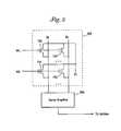
- FIG. 3an illustration of how individual memory cells 150 , 152 , 154 and 156 in the mini array 202 are coupled to sense amplifier 206 is shown.
- word lines WLare coupled to control gates of memory cells 150 , 152 , 154 and 156 to selectively activate memory cells 150 , 152 , 154 and 156 .
- a source line SLis also coupled to memory cells 150 , 152 , 154 and 156 .
- each memory cell 150 , 152 , 154 and 156is coupled to sense amplifier 206 with a respective bit line BL.
- Sense amplifier 206may be a current sense amplifier or a voltage sense amplifier. In FIG.
- the mini array 202could have as many memory cells as there are operating parameters and the mini array 202 of the present invention is not limited to four memory cells.
- Local latches 220 ( a-n )may also be used in determining the desired operating parameters stored in the mini array 202 . This is done by selectively applying different settings to local latches 220 ( a-n ) and then monitoring their effects on the memory. Once a desired effect is achieved in a local latch, a write operation is used to store the setting to an associated memory cell in the mini array 202 for future use.
- an interior bus 221 of the flash memoryis used to provide the operating parameter settings. This is illustrated in FIG. 4 . As illustrated, the interior bus 221 couples the control circuitry 116 to local latches 220 ( a-n ).
- the control circuitry 116 in this embodimentprovides the operating parameter settings to local latches 220 ( a-n ).
- an external bus(not shown) is coupled to the local latches! 220 ( a-n ) to provide the operating parameter settings.
- the present inventionalso allows product engineers to conduct margin read test modes on memory cells in the mini array 202 .
- margin read test modescannot be done effectively on the fuse systems of the prior art.
- a margin read test modeis performed on a memory cell to predict how it will perform over time.
- the voltage marginis the actual voltage range between a programmed cell and a sense amplifier trigger level. By knowing the performance shifts over environmental changes and age, the margin read test allows product engineers to forecast data retention.
- Margin read test modesare also referred to as testing cell margins.
- Control circuitry 116is coupled to a plurality of latches 220 ( a-n ). Control circuitry 116 is also coupled to an optional multiplexer 218 . Multiplexer 218 selectively couples each operating parameter that is output from sense amplifier 206 to an associated latch.
- sense amplifier 206is coupled to the primary array 240 to read memory cells. The primary array 240 contains the array blocks 204 ( a-d ).
- Test circuitry 250in this embodiment, is coupled to the mini array 202 to vary word line WL voltage to conduct margin read test modes. In another embodiment, test circuitry 250 is coupled to sense amplifier 206 to vary the sense amplifier 206 trigger timing. This is another way the margin read test modes are conducted.
- a flash memory device having a mini array to store operating parameterscomprises at least one array block of memory, one or more local latches to store one or more operating parameters and a mini array of non-volatile memory cells.
- the mini arrayis used to store the one or more operating parameters.
- the one or more operating parametersare retrieved from the mini array and stored in associated local latches.
Landscapes
- Read Only Memory (AREA)
Abstract
Description
Claims (10)
Priority Applications (1)
| Application Number | Priority Date | Filing Date | Title |
|---|---|---|---|
| US10/375,477US6614690B2 (en) | 2001-08-13 | 2003-02-26 | Non-volatile memory having a control mini-array |
Applications Claiming Priority (2)
| Application Number | Priority Date | Filing Date | Title |
|---|---|---|---|
| US09/928,580US6614689B2 (en) | 2001-08-13 | 2001-08-13 | Non-volatile memory having a control mini-array |
| US10/375,477US6614690B2 (en) | 2001-08-13 | 2003-02-26 | Non-volatile memory having a control mini-array |
Related Parent Applications (1)
| Application Number | Title | Priority Date | Filing Date |
|---|---|---|---|
| US09/928,580DivisionUS6614689B2 (en) | 2001-08-13 | 2001-08-13 | Non-volatile memory having a control mini-array |
Publications (2)
| Publication Number | Publication Date |
|---|---|
| US20030128590A1 US20030128590A1 (en) | 2003-07-10 |
| US6614690B2true US6614690B2 (en) | 2003-09-02 |
Family
ID=25456467
Family Applications (2)
| Application Number | Title | Priority Date | Filing Date |
|---|---|---|---|
| US09/928,580Expired - LifetimeUS6614689B2 (en) | 2001-08-13 | 2001-08-13 | Non-volatile memory having a control mini-array |
| US10/375,477Expired - LifetimeUS6614690B2 (en) | 2001-08-13 | 2003-02-26 | Non-volatile memory having a control mini-array |
Family Applications Before (1)
| Application Number | Title | Priority Date | Filing Date |
|---|---|---|---|
| US09/928,580Expired - LifetimeUS6614689B2 (en) | 2001-08-13 | 2001-08-13 | Non-volatile memory having a control mini-array |
Country Status (1)
| Country | Link |
|---|---|
| US (2) | US6614689B2 (en) |
Cited By (13)
| Publication number | Priority date | Publication date | Assignee | Title |
|---|---|---|---|---|
| US20030188091A1 (en)* | 2002-03-27 | 2003-10-02 | Wyatt Stewart R. | Exchanging operation parameters between a data storage device and a controller |
| US20040243909A1 (en)* | 2003-05-08 | 2004-12-02 | Micron Technology, Inc. | Error detection, documentation, and correction in a flash memory device |
| US6950353B1 (en) | 2005-02-01 | 2005-09-27 | International Business Machines Corporation | Cell data margin test with dummy cell |
| US20060158938A1 (en)* | 2005-01-19 | 2006-07-20 | Saifun Semiconductors, Ltd. | Method, circuit and systems for erasing one or more non-volatile memory cells |
| US7535765B2 (en) | 2004-12-09 | 2009-05-19 | Saifun Semiconductors Ltd. | Non-volatile memory device and method for reading cells |
| US7590001B2 (en) | 2007-12-18 | 2009-09-15 | Saifun Semiconductors Ltd. | Flash memory with optimized write sector spares |
| US7605579B2 (en) | 2006-09-18 | 2009-10-20 | Saifun Semiconductors Ltd. | Measuring and controlling current consumption and output current of charge pumps |
| US7638835B2 (en) | 2006-02-28 | 2009-12-29 | Saifun Semiconductors Ltd. | Double density NROM with nitride strips (DDNS) |
| US7743230B2 (en) | 2003-01-31 | 2010-06-22 | Saifun Semiconductors Ltd. | Memory array programming circuit and a method for using the circuit |
| US7808818B2 (en) | 2006-01-12 | 2010-10-05 | Saifun Semiconductors Ltd. | Secondary injection for NROM |
| US20110032036A1 (en)* | 2002-06-05 | 2011-02-10 | Stmicroelectronics, Inc. | Performance tuning using encoded performance parameter information |
| US20140269092A1 (en)* | 2013-03-15 | 2014-09-18 | West Virginia University | Continuous-time floating gate memory cell programming |
| US20140269131A1 (en)* | 2013-03-14 | 2014-09-18 | Ravindraraj Ramaraju | Memory with power savings for unnecessary reads |
Families Citing this family (22)
| Publication number | Priority date | Publication date | Assignee | Title |
|---|---|---|---|---|
| ITRM20010556A1 (en)* | 2001-09-12 | 2003-03-12 | Micron Technology Inc | DECODER TO DECODE SWITCHING COMMANDS IN INTEGRATED CIRCUIT TEST MODE. |
| JP4463021B2 (en)* | 2003-06-30 | 2010-05-12 | 株式会社リコー | Information processing apparatus, device control method, and recording medium |
| US20050071610A1 (en)* | 2003-09-30 | 2005-03-31 | International Business Machines Corporation | Method and apparatus for debug support for individual instructions and memory locations |
| US20050204091A1 (en)* | 2004-03-11 | 2005-09-15 | Kilbuck Kevin M. | Non-volatile memory with synchronous DRAM interface |
| CN100437458C (en)* | 2004-07-12 | 2008-11-26 | 株式会社东芝 | Storage device and host apparatus |
| BRPI0510494B8 (en) | 2004-07-12 | 2022-06-28 | Kk Toshiba Toshiba Corporation | STORAGE DEVICE AND HOST DEVICE |
| US7447847B2 (en)* | 2004-07-19 | 2008-11-04 | Micron Technology, Inc. | Memory device trims |
| DE602005021344D1 (en)* | 2005-07-28 | 2010-07-01 | St Microelectronics Srl | Configure a multi-bit flash memory |
| US7463520B2 (en)* | 2006-03-24 | 2008-12-09 | Micron Technology, Inc. | Memory device with variable trim settings |
| JP5016841B2 (en)* | 2006-04-26 | 2012-09-05 | 株式会社東芝 | Nonvolatile semiconductor memory device |
| EP1867723A1 (en)* | 2006-06-16 | 2007-12-19 | Genoplante-Valor | Plants with increased tolerance to water deficit |
| JP4425250B2 (en) | 2006-08-15 | 2010-03-03 | Okiセミコンダクタ株式会社 | Semiconductor non-volatile memory |
| KR100849715B1 (en) | 2006-11-07 | 2008-08-01 | 주식회사 하이닉스반도체 | NAND type flash memory device having global page buffer and method for reading data thereof |
| JP4921953B2 (en)* | 2006-12-25 | 2012-04-25 | 株式会社東芝 | Semiconductor integrated circuit device and semiconductor memory device test method |
| KR100823169B1 (en)* | 2007-01-25 | 2008-04-18 | 삼성전자주식회사 | Flash memory system with improved operating characteristics and access method thereof |
| JP2008204582A (en)* | 2007-02-22 | 2008-09-04 | Elpida Memory Inc | Nonvolatile ram |
| KR100843242B1 (en)* | 2007-04-04 | 2008-07-02 | 삼성전자주식회사 | Flash memory device and driving method thereof |
| US7765426B2 (en)* | 2007-06-07 | 2010-07-27 | Micron Technology, Inc. | Emerging bad block detection |
| US8144517B2 (en)* | 2008-02-22 | 2012-03-27 | Samsung Electronics Co., Ltd. | Multilayered nonvolatile memory with adaptive control |
| KR101571763B1 (en) | 2008-07-07 | 2015-12-07 | 삼성전자주식회사 | Semiconductor memory device having adaptive control scheme and Operating Method of the same |
| KR100977717B1 (en)* | 2009-01-19 | 2010-08-24 | 주식회사 하이닉스반도체 | Nonvolatile Memory Devices and Copyback Methods |
| US11188244B2 (en)* | 2020-04-14 | 2021-11-30 | Micron Technology, Inc. | Adjusting trim settings to improve memory performance or reliability |
Citations (7)
| Publication number | Priority date | Publication date | Assignee | Title |
|---|---|---|---|---|
| US5801985A (en) | 1995-07-28 | 1998-09-01 | Micron Technology, Inc. | Memory system having programmable control parameters |
| US5864499A (en) | 1995-07-28 | 1999-01-26 | Micron Technology, Inc. | Non-volatile data storage unit and method of controlling same |
| US5880996A (en) | 1995-07-28 | 1999-03-09 | Micron Technology, Inc. | Memory system having non-volatile data storage structure for memory control parameters and method |
| US5959445A (en)* | 1995-09-29 | 1999-09-28 | Intel Corporation | Static, high-sensitivity, fuse-based storage cell |
| US6141247A (en) | 1997-10-24 | 2000-10-31 | Micron Technology, Inc. | Non-volatile data storage unit and method of controlling same |
| US6510076B1 (en)* | 2002-02-12 | 2003-01-21 | Pmc-Sierra, Inc. | Variable read/write margin high-performance soft-error tolerant SRAM bit cell |
| US6535434B2 (en)* | 2001-04-05 | 2003-03-18 | Saifun Semiconductors Ltd. | Architecture and scheme for a non-strobed read sequence |
- 2001
- 2001-08-13USUS09/928,580patent/US6614689B2/ennot_activeExpired - Lifetime
- 2003
- 2003-02-26USUS10/375,477patent/US6614690B2/ennot_activeExpired - Lifetime
Patent Citations (8)
| Publication number | Priority date | Publication date | Assignee | Title |
|---|---|---|---|---|
| US5801985A (en) | 1995-07-28 | 1998-09-01 | Micron Technology, Inc. | Memory system having programmable control parameters |
| US5864499A (en) | 1995-07-28 | 1999-01-26 | Micron Technology, Inc. | Non-volatile data storage unit and method of controlling same |
| US5880996A (en) | 1995-07-28 | 1999-03-09 | Micron Technology, Inc. | Memory system having non-volatile data storage structure for memory control parameters and method |
| US6272586B1 (en) | 1995-07-28 | 2001-08-07 | Micron Technology, Inc. | Memory system having programmable control parameters |
| US5959445A (en)* | 1995-09-29 | 1999-09-28 | Intel Corporation | Static, high-sensitivity, fuse-based storage cell |
| US6141247A (en) | 1997-10-24 | 2000-10-31 | Micron Technology, Inc. | Non-volatile data storage unit and method of controlling same |
| US6535434B2 (en)* | 2001-04-05 | 2003-03-18 | Saifun Semiconductors Ltd. | Architecture and scheme for a non-strobed read sequence |
| US6510076B1 (en)* | 2002-02-12 | 2003-01-21 | Pmc-Sierra, Inc. | Variable read/write margin high-performance soft-error tolerant SRAM bit cell |
Cited By (25)
| Publication number | Priority date | Publication date | Assignee | Title |
|---|---|---|---|---|
| US6851018B2 (en)* | 2002-03-27 | 2005-02-01 | Hewlett-Packard Development Company, L.P. | Exchanging operation parameters between a data storage device and a controller |
| US20030188091A1 (en)* | 2002-03-27 | 2003-10-02 | Wyatt Stewart R. | Exchanging operation parameters between a data storage device and a controller |
| US20110032036A1 (en)* | 2002-06-05 | 2011-02-10 | Stmicroelectronics, Inc. | Performance tuning using encoded performance parameter information |
| US7743230B2 (en) | 2003-01-31 | 2010-06-22 | Saifun Semiconductors Ltd. | Memory array programming circuit and a method for using the circuit |
| US20110010583A1 (en)* | 2003-05-08 | 2011-01-13 | Micron Technology, Inc. | Error detection, documentation, and correction in a flash memory device |
| US7676710B2 (en) | 2003-05-08 | 2010-03-09 | Micron Technology, Inc. | Error detection, documentation, and correction in a flash memory device |
| US20060236207A1 (en)* | 2003-05-08 | 2006-10-19 | Micron Technology, Inc. | Error detection, documentation, and correction in a flash memory device |
| US20060242485A1 (en)* | 2003-05-08 | 2006-10-26 | Micron Technology, Inc. | Error detection, documentation, and correction in a flash memory device |
| US7203874B2 (en) | 2003-05-08 | 2007-04-10 | Micron Technology, Inc. | Error detection, documentation, and correction in a flash memory device |
| US8037381B2 (en) | 2003-05-08 | 2011-10-11 | Micron Technology, Inc. | Error detection, documentation, and correction in a flash memory device |
| US20040243909A1 (en)* | 2003-05-08 | 2004-12-02 | Micron Technology, Inc. | Error detection, documentation, and correction in a flash memory device |
| US7797597B2 (en) | 2003-05-08 | 2010-09-14 | Micron Technology , Inc. | Error detection, documentation, and correction in a flash memory device |
| US7535765B2 (en) | 2004-12-09 | 2009-05-19 | Saifun Semiconductors Ltd. | Non-volatile memory device and method for reading cells |
| US20060158938A1 (en)* | 2005-01-19 | 2006-07-20 | Saifun Semiconductors, Ltd. | Method, circuit and systems for erasing one or more non-volatile memory cells |
| US20060181934A1 (en)* | 2005-01-19 | 2006-08-17 | Saifun Semiconductors, Ltd. | Methods for preventing fixed pattern programming |
| US7369440B2 (en)* | 2005-01-19 | 2008-05-06 | Saifun Semiconductors Ltd. | Method, circuit and systems for erasing one or more non-volatile memory cells |
| US6950353B1 (en) | 2005-02-01 | 2005-09-27 | International Business Machines Corporation | Cell data margin test with dummy cell |
| US7808818B2 (en) | 2006-01-12 | 2010-10-05 | Saifun Semiconductors Ltd. | Secondary injection for NROM |
| US7638835B2 (en) | 2006-02-28 | 2009-12-29 | Saifun Semiconductors Ltd. | Double density NROM with nitride strips (DDNS) |
| US7605579B2 (en) | 2006-09-18 | 2009-10-20 | Saifun Semiconductors Ltd. | Measuring and controlling current consumption and output current of charge pumps |
| US7590001B2 (en) | 2007-12-18 | 2009-09-15 | Saifun Semiconductors Ltd. | Flash memory with optimized write sector spares |
| US20140269131A1 (en)* | 2013-03-14 | 2014-09-18 | Ravindraraj Ramaraju | Memory with power savings for unnecessary reads |
| US9117498B2 (en)* | 2013-03-14 | 2015-08-25 | Freescale Semiconductor, Inc. | Memory with power savings for unnecessary reads |
| US20140269092A1 (en)* | 2013-03-15 | 2014-09-18 | West Virginia University | Continuous-time floating gate memory cell programming |
| US9218883B2 (en)* | 2013-03-15 | 2015-12-22 | West Virginia University | Continuous-time floating gate memory cell programming |
Also Published As
| Publication number | Publication date |
|---|---|
| US20030128590A1 (en) | 2003-07-10 |
| US6614689B2 (en) | 2003-09-02 |
| US20030031056A1 (en) | 2003-02-13 |
Similar Documents
| Publication | Publication Date | Title |
|---|---|---|
| US6614690B2 (en) | Non-volatile memory having a control mini-array | |
| US5627780A (en) | Testing a non-volatile memory | |
| JP3730423B2 (en) | Semiconductor memory device | |
| US6870770B2 (en) | Method and architecture to calibrate read operations in synchronous flash memory | |
| US5950224A (en) | Electrically modifiable non-volatile memory circuit having means for autonomous refreshing dependent upon on periodic clock pulses | |
| US6538924B2 (en) | Semiconductor integrated circuit | |
| KR100285063B1 (en) | How to erase and write a synchronous flash memory device that shares a system bus with a synchronous RAM device | |
| US7551510B2 (en) | Memory block reallocation in a flash memory device | |
| JP2006351192A (en) | Method for reducing interference in non-volatile memory | |
| JP2019121414A (en) | Semiconductor memory device | |
| US6188603B1 (en) | Nonvolatile memory device | |
| JP3542637B2 (en) | Current measuring method and microcontroller system | |
| KR20130072712A (en) | Nonvolatile memory device and method for controlling the same | |
| JPH10199263A (en) | Non-volatile semiconductor memory device | |
| US7376024B2 (en) | User configurable commands for flash memory | |
| US5917750A (en) | Nonvolatile semiconductor memory with a protect circuit | |
| JP3123983B2 (en) | Nonvolatile semiconductor memory device | |
| KR20070084468A (en) | Information setting method of nonvolatile memory and nonvolatile memory |
Legal Events
| Date | Code | Title | Description |
|---|---|---|---|
| FEPP | Fee payment procedure | Free format text:PAYOR NUMBER ASSIGNED (ORIGINAL EVENT CODE: ASPN); ENTITY STATUS OF PATENT OWNER: LARGE ENTITY | |
| STCF | Information on status: patent grant | Free format text:PATENTED CASE | |
| FPAY | Fee payment | Year of fee payment:4 | |
| FPAY | Fee payment | Year of fee payment:8 | |
| FPAY | Fee payment | Year of fee payment:12 | |
| AS | Assignment | Owner name:U.S. BANK NATIONAL ASSOCIATION, AS COLLATERAL AGENT, CALIFORNIA Free format text:SECURITY INTEREST;ASSIGNOR:MICRON TECHNOLOGY, INC.;REEL/FRAME:038669/0001 Effective date:20160426 Owner name:U.S. BANK NATIONAL ASSOCIATION, AS COLLATERAL AGEN Free format text:SECURITY INTEREST;ASSIGNOR:MICRON TECHNOLOGY, INC.;REEL/FRAME:038669/0001 Effective date:20160426 | |
| AS | Assignment | Owner name:MORGAN STANLEY SENIOR FUNDING, INC., AS COLLATERAL AGENT, MARYLAND Free format text:PATENT SECURITY AGREEMENT;ASSIGNOR:MICRON TECHNOLOGY, INC.;REEL/FRAME:038954/0001 Effective date:20160426 Owner name:MORGAN STANLEY SENIOR FUNDING, INC., AS COLLATERAL Free format text:PATENT SECURITY AGREEMENT;ASSIGNOR:MICRON TECHNOLOGY, INC.;REEL/FRAME:038954/0001 Effective date:20160426 | |
| AS | Assignment | Owner name:U.S. BANK NATIONAL ASSOCIATION, AS COLLATERAL AGENT, CALIFORNIA Free format text:CORRECTIVE ASSIGNMENT TO CORRECT THE REPLACE ERRONEOUSLY FILED PATENT #7358718 WITH THE CORRECT PATENT #7358178 PREVIOUSLY RECORDED ON REEL 038669 FRAME 0001. ASSIGNOR(S) HEREBY CONFIRMS THE SECURITY INTEREST;ASSIGNOR:MICRON TECHNOLOGY, INC.;REEL/FRAME:043079/0001 Effective date:20160426 Owner name:U.S. BANK NATIONAL ASSOCIATION, AS COLLATERAL AGEN Free format text:CORRECTIVE ASSIGNMENT TO CORRECT THE REPLACE ERRONEOUSLY FILED PATENT #7358718 WITH THE CORRECT PATENT #7358178 PREVIOUSLY RECORDED ON REEL 038669 FRAME 0001. ASSIGNOR(S) HEREBY CONFIRMS THE SECURITY INTEREST;ASSIGNOR:MICRON TECHNOLOGY, INC.;REEL/FRAME:043079/0001 Effective date:20160426 | |
| AS | Assignment | Owner name:JPMORGAN CHASE BANK, N.A., AS COLLATERAL AGENT, ILLINOIS Free format text:SECURITY INTEREST;ASSIGNORS:MICRON TECHNOLOGY, INC.;MICRON SEMICONDUCTOR PRODUCTS, INC.;REEL/FRAME:047540/0001 Effective date:20180703 Owner name:JPMORGAN CHASE BANK, N.A., AS COLLATERAL AGENT, IL Free format text:SECURITY INTEREST;ASSIGNORS:MICRON TECHNOLOGY, INC.;MICRON SEMICONDUCTOR PRODUCTS, INC.;REEL/FRAME:047540/0001 Effective date:20180703 | |
| AS | Assignment | Owner name:MICRON TECHNOLOGY, INC., IDAHO Free format text:RELEASE BY SECURED PARTY;ASSIGNOR:U.S. BANK NATIONAL ASSOCIATION, AS COLLATERAL AGENT;REEL/FRAME:047243/0001 Effective date:20180629 | |
| AS | Assignment | Owner name:MICRON TECHNOLOGY, INC., IDAHO Free format text:RELEASE BY SECURED PARTY;ASSIGNOR:MORGAN STANLEY SENIOR FUNDING, INC., AS COLLATERAL AGENT;REEL/FRAME:050937/0001 Effective date:20190731 | |
| AS | Assignment | Owner name:MICRON TECHNOLOGY, INC., IDAHO Free format text:RELEASE BY SECURED PARTY;ASSIGNOR:JPMORGAN CHASE BANK, N.A., AS COLLATERAL AGENT;REEL/FRAME:051028/0001 Effective date:20190731 Owner name:MICRON SEMICONDUCTOR PRODUCTS, INC., IDAHO Free format text:RELEASE BY SECURED PARTY;ASSIGNOR:JPMORGAN CHASE BANK, N.A., AS COLLATERAL AGENT;REEL/FRAME:051028/0001 Effective date:20190731 |