US6614103B1 - Plastic packaging of LED arrays - Google Patents
Plastic packaging of LED arraysDownload PDFInfo
- Publication number
- US6614103B1 US6614103B1US09/654,163US65416300AUS6614103B1US 6614103 B1US6614103 B1US 6614103B1US 65416300 AUS65416300 AUS 65416300AUS 6614103 B1US6614103 B1US 6614103B1
- Authority
- US
- United States
- Prior art keywords
- module
- flexible base
- rigid
- rigid carrier
- carrier
- Prior art date
- Legal status (The legal status is an assumption and is not a legal conclusion. Google has not performed a legal analysis and makes no representation as to the accuracy of the status listed.)
- Expired - Lifetime, expires
Links
Images


Classifications
- H—ELECTRICITY
- H01—ELECTRIC ELEMENTS
- H01L—SEMICONDUCTOR DEVICES NOT COVERED BY CLASS H10
- H01L23/00—Details of semiconductor or other solid state devices
- H01L23/12—Mountings, e.g. non-detachable insulating substrates
- H01L23/13—Mountings, e.g. non-detachable insulating substrates characterised by the shape
- H—ELECTRICITY
- H01—ELECTRIC ELEMENTS
- H01L—SEMICONDUCTOR DEVICES NOT COVERED BY CLASS H10
- H01L23/00—Details of semiconductor or other solid state devices
- H01L23/34—Arrangements for cooling, heating, ventilating or temperature compensation ; Temperature sensing arrangements
- H01L23/36—Selection of materials, or shaping, to facilitate cooling or heating, e.g. heatsinks
- H01L23/367—Cooling facilitated by shape of device
- H01L23/3677—Wire-like or pin-like cooling fins or heat sinks
- H—ELECTRICITY
- H01—ELECTRIC ELEMENTS
- H01L—SEMICONDUCTOR DEVICES NOT COVERED BY CLASS H10
- H01L23/00—Details of semiconductor or other solid state devices
- H01L23/48—Arrangements for conducting electric current to or from the solid state body in operation, e.g. leads, terminal arrangements ; Selection of materials therefor
- H01L23/488—Arrangements for conducting electric current to or from the solid state body in operation, e.g. leads, terminal arrangements ; Selection of materials therefor consisting of soldered or bonded constructions
- H01L23/498—Leads, i.e. metallisations or lead-frames on insulating substrates, e.g. chip carriers
- H01L23/49833—Leads, i.e. metallisations or lead-frames on insulating substrates, e.g. chip carriers the chip support structure consisting of a plurality of insulating substrates
- H—ELECTRICITY
- H01—ELECTRIC ELEMENTS
- H01L—SEMICONDUCTOR DEVICES NOT COVERED BY CLASS H10
- H01L24/00—Arrangements for connecting or disconnecting semiconductor or solid-state bodies; Methods or apparatus related thereto
- H01L24/93—Batch processes
- H01L24/95—Batch processes at chip-level, i.e. with connecting carried out on a plurality of singulated devices, i.e. on diced chips
- H01L24/97—Batch processes at chip-level, i.e. with connecting carried out on a plurality of singulated devices, i.e. on diced chips the devices being connected to a common substrate, e.g. interposer, said common substrate being separable into individual assemblies after connecting
- H—ELECTRICITY
- H01—ELECTRIC ELEMENTS
- H01L—SEMICONDUCTOR DEVICES NOT COVERED BY CLASS H10
- H01L2224/00—Indexing scheme for arrangements for connecting or disconnecting semiconductor or solid-state bodies and methods related thereto as covered by H01L24/00
- H01L2224/01—Means for bonding being attached to, or being formed on, the surface to be connected, e.g. chip-to-package, die-attach, "first-level" interconnects; Manufacturing methods related thereto
- H01L2224/02—Bonding areas; Manufacturing methods related thereto
- H01L2224/04—Structure, shape, material or disposition of the bonding areas prior to the connecting process
- H01L2224/05—Structure, shape, material or disposition of the bonding areas prior to the connecting process of an individual bonding area
- H01L2224/0554—External layer
- H01L2224/05599—Material
- H—ELECTRICITY
- H01—ELECTRIC ELEMENTS
- H01L—SEMICONDUCTOR DEVICES NOT COVERED BY CLASS H10
- H01L2224/00—Indexing scheme for arrangements for connecting or disconnecting semiconductor or solid-state bodies and methods related thereto as covered by H01L24/00
- H01L2224/01—Means for bonding being attached to, or being formed on, the surface to be connected, e.g. chip-to-package, die-attach, "first-level" interconnects; Manufacturing methods related thereto
- H01L2224/10—Bump connectors; Manufacturing methods related thereto
- H01L2224/15—Structure, shape, material or disposition of the bump connectors after the connecting process
- H01L2224/16—Structure, shape, material or disposition of the bump connectors after the connecting process of an individual bump connector
- H—ELECTRICITY
- H01—ELECTRIC ELEMENTS
- H01L—SEMICONDUCTOR DEVICES NOT COVERED BY CLASS H10
- H01L2224/00—Indexing scheme for arrangements for connecting or disconnecting semiconductor or solid-state bodies and methods related thereto as covered by H01L24/00
- H01L2224/01—Means for bonding being attached to, or being formed on, the surface to be connected, e.g. chip-to-package, die-attach, "first-level" interconnects; Manufacturing methods related thereto
- H01L2224/42—Wire connectors; Manufacturing methods related thereto
- H01L2224/44—Structure, shape, material or disposition of the wire connectors prior to the connecting process
- H01L2224/45—Structure, shape, material or disposition of the wire connectors prior to the connecting process of an individual wire connector
- H01L2224/45001—Core members of the connector
- H01L2224/45099—Material
- H—ELECTRICITY
- H01—ELECTRIC ELEMENTS
- H01L—SEMICONDUCTOR DEVICES NOT COVERED BY CLASS H10
- H01L2224/00—Indexing scheme for arrangements for connecting or disconnecting semiconductor or solid-state bodies and methods related thereto as covered by H01L24/00
- H01L2224/01—Means for bonding being attached to, or being formed on, the surface to be connected, e.g. chip-to-package, die-attach, "first-level" interconnects; Manufacturing methods related thereto
- H01L2224/42—Wire connectors; Manufacturing methods related thereto
- H01L2224/47—Structure, shape, material or disposition of the wire connectors after the connecting process
- H01L2224/48—Structure, shape, material or disposition of the wire connectors after the connecting process of an individual wire connector
- H01L2224/4805—Shape
- H01L2224/4809—Loop shape
- H01L2224/48091—Arched
- H—ELECTRICITY
- H01—ELECTRIC ELEMENTS
- H01L—SEMICONDUCTOR DEVICES NOT COVERED BY CLASS H10
- H01L2224/00—Indexing scheme for arrangements for connecting or disconnecting semiconductor or solid-state bodies and methods related thereto as covered by H01L24/00
- H01L2224/80—Methods for connecting semiconductor or other solid state bodies using means for bonding being attached to, or being formed on, the surface to be connected
- H01L2224/85—Methods for connecting semiconductor or other solid state bodies using means for bonding being attached to, or being formed on, the surface to be connected using a wire connector
- H01L2224/8538—Bonding interfaces outside the semiconductor or solid-state body
- H01L2224/85399—Material
- H—ELECTRICITY
- H01—ELECTRIC ELEMENTS
- H01L—SEMICONDUCTOR DEVICES NOT COVERED BY CLASS H10
- H01L2224/00—Indexing scheme for arrangements for connecting or disconnecting semiconductor or solid-state bodies and methods related thereto as covered by H01L24/00
- H01L2224/93—Batch processes
- H01L2224/95—Batch processes at chip-level, i.e. with connecting carried out on a plurality of singulated devices, i.e. on diced chips
- H01L2224/97—Batch processes at chip-level, i.e. with connecting carried out on a plurality of singulated devices, i.e. on diced chips the devices being connected to a common substrate, e.g. interposer, said common substrate being separable into individual assemblies after connecting
- H—ELECTRICITY
- H01—ELECTRIC ELEMENTS
- H01L—SEMICONDUCTOR DEVICES NOT COVERED BY CLASS H10
- H01L24/00—Arrangements for connecting or disconnecting semiconductor or solid-state bodies; Methods or apparatus related thereto
- H01L24/01—Means for bonding being attached to, or being formed on, the surface to be connected, e.g. chip-to-package, die-attach, "first-level" interconnects; Manufacturing methods related thereto
- H01L24/42—Wire connectors; Manufacturing methods related thereto
- H01L24/47—Structure, shape, material or disposition of the wire connectors after the connecting process
- H01L24/48—Structure, shape, material or disposition of the wire connectors after the connecting process of an individual wire connector
- H—ELECTRICITY
- H01—ELECTRIC ELEMENTS
- H01L—SEMICONDUCTOR DEVICES NOT COVERED BY CLASS H10
- H01L2924/00—Indexing scheme for arrangements or methods for connecting or disconnecting semiconductor or solid-state bodies as covered by H01L24/00
- H01L2924/0001—Technical content checked by a classifier
- H01L2924/00014—Technical content checked by a classifier the subject-matter covered by the group, the symbol of which is combined with the symbol of this group, being disclosed without further technical details
- H—ELECTRICITY
- H01—ELECTRIC ELEMENTS
- H01L—SEMICONDUCTOR DEVICES NOT COVERED BY CLASS H10
- H01L2924/00—Indexing scheme for arrangements or methods for connecting or disconnecting semiconductor or solid-state bodies as covered by H01L24/00
- H01L2924/01—Chemical elements
- H01L2924/01005—Boron [B]
- H—ELECTRICITY
- H01—ELECTRIC ELEMENTS
- H01L—SEMICONDUCTOR DEVICES NOT COVERED BY CLASS H10
- H01L2924/00—Indexing scheme for arrangements or methods for connecting or disconnecting semiconductor or solid-state bodies as covered by H01L24/00
- H01L2924/01—Chemical elements
- H01L2924/01006—Carbon [C]
- H—ELECTRICITY
- H01—ELECTRIC ELEMENTS
- H01L—SEMICONDUCTOR DEVICES NOT COVERED BY CLASS H10
- H01L2924/00—Indexing scheme for arrangements or methods for connecting or disconnecting semiconductor or solid-state bodies as covered by H01L24/00
- H01L2924/01—Chemical elements
- H01L2924/01013—Aluminum [Al]
- H—ELECTRICITY
- H01—ELECTRIC ELEMENTS
- H01L—SEMICONDUCTOR DEVICES NOT COVERED BY CLASS H10
- H01L2924/00—Indexing scheme for arrangements or methods for connecting or disconnecting semiconductor or solid-state bodies as covered by H01L24/00
- H01L2924/01—Chemical elements
- H01L2924/01015—Phosphorus [P]
- H—ELECTRICITY
- H01—ELECTRIC ELEMENTS
- H01L—SEMICONDUCTOR DEVICES NOT COVERED BY CLASS H10
- H01L2924/00—Indexing scheme for arrangements or methods for connecting or disconnecting semiconductor or solid-state bodies as covered by H01L24/00
- H01L2924/01—Chemical elements
- H01L2924/01023—Vanadium [V]
- H—ELECTRICITY
- H01—ELECTRIC ELEMENTS
- H01L—SEMICONDUCTOR DEVICES NOT COVERED BY CLASS H10
- H01L2924/00—Indexing scheme for arrangements or methods for connecting or disconnecting semiconductor or solid-state bodies as covered by H01L24/00
- H01L2924/01—Chemical elements
- H01L2924/01027—Cobalt [Co]
- H—ELECTRICITY
- H01—ELECTRIC ELEMENTS
- H01L—SEMICONDUCTOR DEVICES NOT COVERED BY CLASS H10
- H01L2924/00—Indexing scheme for arrangements or methods for connecting or disconnecting semiconductor or solid-state bodies as covered by H01L24/00
- H01L2924/01—Chemical elements
- H01L2924/01029—Copper [Cu]
- H—ELECTRICITY
- H01—ELECTRIC ELEMENTS
- H01L—SEMICONDUCTOR DEVICES NOT COVERED BY CLASS H10
- H01L2924/00—Indexing scheme for arrangements or methods for connecting or disconnecting semiconductor or solid-state bodies as covered by H01L24/00
- H01L2924/01—Chemical elements
- H01L2924/01033—Arsenic [As]
- H—ELECTRICITY
- H01—ELECTRIC ELEMENTS
- H01L—SEMICONDUCTOR DEVICES NOT COVERED BY CLASS H10
- H01L2924/00—Indexing scheme for arrangements or methods for connecting or disconnecting semiconductor or solid-state bodies as covered by H01L24/00
- H01L2924/01—Chemical elements
- H01L2924/01039—Yttrium [Y]
- H—ELECTRICITY
- H01—ELECTRIC ELEMENTS
- H01L—SEMICONDUCTOR DEVICES NOT COVERED BY CLASS H10
- H01L2924/00—Indexing scheme for arrangements or methods for connecting or disconnecting semiconductor or solid-state bodies as covered by H01L24/00
- H01L2924/01—Chemical elements
- H01L2924/01047—Silver [Ag]
- H—ELECTRICITY
- H01—ELECTRIC ELEMENTS
- H01L—SEMICONDUCTOR DEVICES NOT COVERED BY CLASS H10
- H01L2924/00—Indexing scheme for arrangements or methods for connecting or disconnecting semiconductor or solid-state bodies as covered by H01L24/00
- H01L2924/01—Chemical elements
- H01L2924/01058—Cerium [Ce]
- H—ELECTRICITY
- H01—ELECTRIC ELEMENTS
- H01L—SEMICONDUCTOR DEVICES NOT COVERED BY CLASS H10
- H01L2924/00—Indexing scheme for arrangements or methods for connecting or disconnecting semiconductor or solid-state bodies as covered by H01L24/00
- H01L2924/01—Chemical elements
- H01L2924/01078—Platinum [Pt]
- H—ELECTRICITY
- H01—ELECTRIC ELEMENTS
- H01L—SEMICONDUCTOR DEVICES NOT COVERED BY CLASS H10
- H01L2924/00—Indexing scheme for arrangements or methods for connecting or disconnecting semiconductor or solid-state bodies as covered by H01L24/00
- H01L2924/01—Chemical elements
- H01L2924/01079—Gold [Au]
- H—ELECTRICITY
- H01—ELECTRIC ELEMENTS
- H01L—SEMICONDUCTOR DEVICES NOT COVERED BY CLASS H10
- H01L2924/00—Indexing scheme for arrangements or methods for connecting or disconnecting semiconductor or solid-state bodies as covered by H01L24/00
- H01L2924/01—Chemical elements
- H01L2924/01082—Lead [Pb]
- H—ELECTRICITY
- H01—ELECTRIC ELEMENTS
- H01L—SEMICONDUCTOR DEVICES NOT COVERED BY CLASS H10
- H01L2924/00—Indexing scheme for arrangements or methods for connecting or disconnecting semiconductor or solid-state bodies as covered by H01L24/00
- H01L2924/013—Alloys
- H01L2924/0132—Binary Alloys
- H01L2924/01322—Eutectic Alloys, i.e. obtained by a liquid transforming into two solid phases
- H—ELECTRICITY
- H01—ELECTRIC ELEMENTS
- H01L—SEMICONDUCTOR DEVICES NOT COVERED BY CLASS H10
- H01L2924/00—Indexing scheme for arrangements or methods for connecting or disconnecting semiconductor or solid-state bodies as covered by H01L24/00
- H01L2924/06—Polymers
- H01L2924/078—Adhesive characteristics other than chemical
- H01L2924/0781—Adhesive characteristics other than chemical being an ohmic electrical conductor
- H01L2924/07811—Extrinsic, i.e. with electrical conductive fillers
- H—ELECTRICITY
- H01—ELECTRIC ELEMENTS
- H01L—SEMICONDUCTOR DEVICES NOT COVERED BY CLASS H10
- H01L2924/00—Indexing scheme for arrangements or methods for connecting or disconnecting semiconductor or solid-state bodies as covered by H01L24/00
- H01L2924/10—Details of semiconductor or other solid state devices to be connected
- H01L2924/102—Material of the semiconductor or solid state bodies
- H01L2924/1025—Semiconducting materials
- H01L2924/1026—Compound semiconductors
- H01L2924/1032—III-V
- H01L2924/10329—Gallium arsenide [GaAs]
- H—ELECTRICITY
- H01—ELECTRIC ELEMENTS
- H01L—SEMICONDUCTOR DEVICES NOT COVERED BY CLASS H10
- H01L2924/00—Indexing scheme for arrangements or methods for connecting or disconnecting semiconductor or solid-state bodies as covered by H01L24/00
- H01L2924/10—Details of semiconductor or other solid state devices to be connected
- H01L2924/11—Device type
- H01L2924/12—Passive devices, e.g. 2 terminal devices
- H01L2924/1204—Optical Diode
- H01L2924/12041—LED
- H—ELECTRICITY
- H01—ELECTRIC ELEMENTS
- H01L—SEMICONDUCTOR DEVICES NOT COVERED BY CLASS H10
- H01L2924/00—Indexing scheme for arrangements or methods for connecting or disconnecting semiconductor or solid-state bodies as covered by H01L24/00
- H01L2924/10—Details of semiconductor or other solid state devices to be connected
- H01L2924/11—Device type
- H01L2924/12—Passive devices, e.g. 2 terminal devices
- H01L2924/1204—Optical Diode
- H01L2924/12042—LASER
- H—ELECTRICITY
- H01—ELECTRIC ELEMENTS
- H01L—SEMICONDUCTOR DEVICES NOT COVERED BY CLASS H10
- H01L2924/00—Indexing scheme for arrangements or methods for connecting or disconnecting semiconductor or solid-state bodies as covered by H01L24/00
- H01L2924/10—Details of semiconductor or other solid state devices to be connected
- H01L2924/11—Device type
- H01L2924/14—Integrated circuits
- H01L2924/143—Digital devices
- H01L2924/1433—Application-specific integrated circuit [ASIC]
- H—ELECTRICITY
- H01—ELECTRIC ELEMENTS
- H01L—SEMICONDUCTOR DEVICES NOT COVERED BY CLASS H10
- H01L2924/00—Indexing scheme for arrangements or methods for connecting or disconnecting semiconductor or solid-state bodies as covered by H01L24/00
- H01L2924/15—Details of package parts other than the semiconductor or other solid state devices to be connected
- H01L2924/151—Die mounting substrate
- H01L2924/1515—Shape
- H01L2924/15153—Shape the die mounting substrate comprising a recess for hosting the device
- H01L2924/15155—Shape the die mounting substrate comprising a recess for hosting the device the shape of the recess being other than a cuboid
- H01L2924/15157—Top view
- H—ELECTRICITY
- H01—ELECTRIC ELEMENTS
- H01L—SEMICONDUCTOR DEVICES NOT COVERED BY CLASS H10
- H01L2924/00—Indexing scheme for arrangements or methods for connecting or disconnecting semiconductor or solid-state bodies as covered by H01L24/00
- H01L2924/15—Details of package parts other than the semiconductor or other solid state devices to be connected
- H01L2924/151—Die mounting substrate
- H01L2924/15165—Monolayer substrate
- H—ELECTRICITY
- H01—ELECTRIC ELEMENTS
- H01L—SEMICONDUCTOR DEVICES NOT COVERED BY CLASS H10
- H01L2924/00—Indexing scheme for arrangements or methods for connecting or disconnecting semiconductor or solid-state bodies as covered by H01L24/00
- H01L2924/15—Details of package parts other than the semiconductor or other solid state devices to be connected
- H01L2924/181—Encapsulation
- H—ELECTRICITY
- H01—ELECTRIC ELEMENTS
- H01L—SEMICONDUCTOR DEVICES NOT COVERED BY CLASS H10
- H01L2924/00—Indexing scheme for arrangements or methods for connecting or disconnecting semiconductor or solid-state bodies as covered by H01L24/00
- H01L2924/19—Details of hybrid assemblies other than the semiconductor or other solid state devices to be connected
- H01L2924/1901—Structure
- H01L2924/1904—Component type
- H01L2924/19041—Component type being a capacitor
- H—ELECTRICITY
- H01—ELECTRIC ELEMENTS
- H01L—SEMICONDUCTOR DEVICES NOT COVERED BY CLASS H10
- H01L2924/00—Indexing scheme for arrangements or methods for connecting or disconnecting semiconductor or solid-state bodies as covered by H01L24/00
- H01L2924/19—Details of hybrid assemblies other than the semiconductor or other solid state devices to be connected
- H01L2924/1901—Structure
- H01L2924/1904—Component type
- H01L2924/19042—Component type being an inductor
- H—ELECTRICITY
- H01—ELECTRIC ELEMENTS
- H01L—SEMICONDUCTOR DEVICES NOT COVERED BY CLASS H10
- H01L2924/00—Indexing scheme for arrangements or methods for connecting or disconnecting semiconductor or solid-state bodies as covered by H01L24/00
- H01L2924/19—Details of hybrid assemblies other than the semiconductor or other solid state devices to be connected
- H01L2924/1901—Structure
- H01L2924/1904—Component type
- H01L2924/19043—Component type being a resistor
- H—ELECTRICITY
- H10—SEMICONDUCTOR DEVICES; ELECTRIC SOLID-STATE DEVICES NOT OTHERWISE PROVIDED FOR
- H10H—INORGANIC LIGHT-EMITTING SEMICONDUCTOR DEVICES HAVING POTENTIAL BARRIERS
- H10H20/00—Individual inorganic light-emitting semiconductor devices having potential barriers, e.g. light-emitting diodes [LED]
- H10H20/80—Constructional details
- H10H20/84—Coatings, e.g. passivation layers or antireflective coatings
- H10H20/841—Reflective coatings, e.g. dielectric Bragg reflectors
- H—ELECTRICITY
- H10—SEMICONDUCTOR DEVICES; ELECTRIC SOLID-STATE DEVICES NOT OTHERWISE PROVIDED FOR
- H10H—INORGANIC LIGHT-EMITTING SEMICONDUCTOR DEVICES HAVING POTENTIAL BARRIERS
- H10H20/00—Individual inorganic light-emitting semiconductor devices having potential barriers, e.g. light-emitting diodes [LED]
- H10H20/80—Constructional details
- H10H20/85—Packages
- H10H20/857—Interconnections, e.g. lead-frames, bond wires or solder balls
- Y—GENERAL TAGGING OF NEW TECHNOLOGICAL DEVELOPMENTS; GENERAL TAGGING OF CROSS-SECTIONAL TECHNOLOGIES SPANNING OVER SEVERAL SECTIONS OF THE IPC; TECHNICAL SUBJECTS COVERED BY FORMER USPC CROSS-REFERENCE ART COLLECTIONS [XRACs] AND DIGESTS
- Y10—TECHNICAL SUBJECTS COVERED BY FORMER USPC
- Y10S—TECHNICAL SUBJECTS COVERED BY FORMER USPC CROSS-REFERENCE ART COLLECTIONS [XRACs] AND DIGESTS
- Y10S362/00—Illumination
- Y10S362/80—Light emitting diode
- Y—GENERAL TAGGING OF NEW TECHNOLOGICAL DEVELOPMENTS; GENERAL TAGGING OF CROSS-SECTIONAL TECHNOLOGIES SPANNING OVER SEVERAL SECTIONS OF THE IPC; TECHNICAL SUBJECTS COVERED BY FORMER USPC CROSS-REFERENCE ART COLLECTIONS [XRACs] AND DIGESTS
- Y10—TECHNICAL SUBJECTS COVERED BY FORMER USPC
- Y10T—TECHNICAL SUBJECTS COVERED BY FORMER US CLASSIFICATION
- Y10T29/00—Metal working
- Y10T29/49—Method of mechanical manufacture
- Y10T29/49002—Electrical device making
- Y10T29/49117—Conductor or circuit manufacturing
- Y10T29/49124—On flat or curved insulated base, e.g., printed circuit, etc.
- Y10T29/49155—Manufacturing circuit on or in base
- Y—GENERAL TAGGING OF NEW TECHNOLOGICAL DEVELOPMENTS; GENERAL TAGGING OF CROSS-SECTIONAL TECHNOLOGIES SPANNING OVER SEVERAL SECTIONS OF THE IPC; TECHNICAL SUBJECTS COVERED BY FORMER USPC CROSS-REFERENCE ART COLLECTIONS [XRACs] AND DIGESTS
- Y10—TECHNICAL SUBJECTS COVERED BY FORMER USPC
- Y10T—TECHNICAL SUBJECTS COVERED BY FORMER US CLASSIFICATION
- Y10T29/00—Metal working
- Y10T29/49—Method of mechanical manufacture
- Y10T29/49002—Electrical device making
- Y10T29/49117—Conductor or circuit manufacturing
- Y10T29/49169—Assembling electrical component directly to terminal or elongated conductor
- Y10T29/49171—Assembling electrical component directly to terminal or elongated conductor with encapsulating
Definitions
- This inventionrelates generally to semiconductor device packaging and specifically to plastic packaging of light emitting diode (“LED”) arrays.
- LEDlight emitting diode
- Semiconductor light emitting diodesare semiconductor chips that are mounted in a package and emit radiation in response to an applied voltage or current. These LEDs are used in a number of commercial applications such as automotive, display, safety/emergency and directed area lighting.
- One type of conventional LEDsis packaged in individual, transparent shells.
- Each shellcontains one LED chip encapsulated by an encapsulating material, such as an epoxy.
- an encapsulating materialsuch as an epoxy.
- the individual shellsare interconnected by connecting the individual LED lead frames with rigid metal lines.
- Such an LED arrayis fragile and difficult to bend into the desired shape due to the rigidity of the connecting metal lines.
- such an LED arraycannot be easily fit into a curved lighting product, such as a round bulb.
- FIG. 1Another type of conventional LED arrays is fabricated on a plastic substrate, as illustrated in FIG. 1 .
- the LED chips or die 1are physically and electrically mounted on cathode leads 3 .
- the top surfaces of the LED chips 1are electrically connected to anode leads 5 with lead wires 7 .
- the lead wiresare attached by known wire bonding techniques to a conductive chip pad.
- the leads 3 , 5comprise a lead frame and may be made of a metal, such as silver plated copper.
- the lead frame and LED chip arrayare contained in a plastic package 9 , such as a LEXAN® package.
- the plastic package 9is filled with an encapsulating material 13 , such as a glass-filled epoxy.
- the package 9contains tapered interior sidewalls 15 which enclose the LED chips 1 , and form a light spreading cavity 17 which ensures cross fluxing of LED light.
- the plastic package 9 and the lead frame 3 , 5are rigid.
- these LED arraysare also rigid and difficult to bend into a desired shape.
- These LED arraysalso cannot be easily fit into a curved lighting product, such as a round bulb.
- the present inventionis directed to overcoming or at least reducing the problems set forth above.
- a flexible circuit modulecomprising at least one rigid carrier, at least one solid state device mounted over a first side of the at least one rigid carrier, a flexible base supporting a second side of the at least one rigid carrier, a conductive interconnect pattern on the flexible base, and a plurality of feed through electrodes extending from the first side to the second side of the at least one rigid carrier and electrically connecting the conductive interconnect pattern with the at least one of a plurality of the solid state devices.
- a method of forming a flexible circuit modulecomprising adhering a first side of at least one rigid carrier over a first side of a flexible module base, forming a conductive interconnect pattern having a first portion over a second side of the flexible module base and a plurality of second portions extending through the flexible module base toward the at least one rigid carrier, and forming at least one solid state device on a second side of the at least one rigid carrier and in electrical contact with the conductive interconnect pattern through the at least one rigid carrier.
- a method of forming a packaged solid state devicecomprising placing at least one conductive element into a mold cavity, filling the mold cavity with a fluid insulating material, solidifying the fluid insulating material to form an insulating carrier, wherein at least two surfaces of the at least one conductive element are exposed after solidification, and placing at least one solid state device on the insulating carrier in contact with one surface of the at least one conductive element.
- FIG. 1is a three dimensional view of a prior art LED array.
- FIG. 2is a side cross sectional view of a carrier according to a first preferred embodiment of the present invention.
- FIG. 3is a side cross sectional view of a carrier according to a second preferred embodiment of the present invention.
- FIG. 4is a side cross sectional view of a carrier according to the second preferred embodiment of the present invention adhered to a flexible base to form a module according to one preferred aspect of the present invention.
- FIG. 5is a side cross sectional view of a carrier according to the second preferred embodiment of the present invention adhered to a flexible base to form a module according to another preferred aspect of the present invention.
- FIG. 6is a side cross sectional view of a module according to the second preferred embodiment of the present invention containing a reflective layer.
- FIG. 7is a side cross sectional view of a module according to the second preferred embodiment of the present invention containing a plurality of LED chips mounted according to one preferred aspect of the present invention.
- FIG. 8is a side cross sectional view of a module according to the second preferred embodiment of the present invention containing a plurality of LED chips mounted according to another preferred aspect of the present invention.
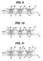
- FIG. 9is a side cross sectional view of a module according to the second preferred embodiment of the present invention containing a plurality of encapsulated LED chips mounted according to one preferred aspect of the present invention.
- FIG. 10is a side cross sectional view of a module according to the second preferred embodiment of the present invention containing a plurality of encapsulated LED chips mounted according to another preferred aspect of the present invention.
- FIG. 11is a side cross sectional view of a module according to the second preferred embodiment of the present invention containing a plurality of lens structures over the LED chips mounted according to one preferred aspect of the present invention.
- FIG. 12is a side cross sectional view of a module according to the second preferred embodiment of the present invention containing a plurality of lens structures over the LED chips mounted according to another preferred aspect of the present invention.
- FIG. 13is a side cross sectional view of a plurality of modules according to the first preferred embodiment of the present invention containing a plurality of lens structures over the LED chips mounted according to one preferred aspect of the present invention.
- FIGS. 14 to 16are side cross sectional views of the steps in a method of forming the carrier according to the first preferred embodiment of the present invention.
- an LED arraythat is packaged such that it may be bent into a desired shape. It is also desirable to obtain a conformal LED array that can easily fit into a variety of differently shaped lighting products, such as spherical, cylindrical or curved products, including a round lamp bulb, a flood light, a cylindrical flashlight or a shaped display.
- a conformal LED array modulemay be provided by placing individual LED chips into rigid carriers and mounting the rigid carriers onto a flexible base.
- the flexible basemay be bent into a desired shape so that the LED array can easily fit into a variety of lighting products.
- the rigid carriercontains feed through electrodes and an optional heat sink which connect to the back side of the LED chips to provide a low thermal resistance for the LED array resulting in longer LED lifetimes.
- An interconnect patternis located on the back side of the flexible base and contains portions that are electrically connected with the feed through electrodes to provide back side electrical connectivity to the LED chips without blocking any light emission from the LED chips.
- FIG. 2illustrates a rigid carrier 21 according to the first preferred embodiment of the present invention.
- the carriermay be made of any electrically insulating material, such as plastic, which is able to resist LED chip operating temperatures without excessive deformation.
- other insulating materialssuch as ceramics may be used instead.
- the carrier 21is formed by molding any moldable plastic or polymer material, such as a thermal set epoxy filled with silica or beryllia.
- Plaskon® SMT-B-1 material supplied by Amoco Electronic Materials, Inc.may be molded into the rigid carrier 21 , as will be described in more detail below.
- the carrier 21may have any desired shape that allows the carrier to house an LED chip.
- the carrier 21has a first side 22 and a second side 23 .
- the carrier 21may have a cup shape with straight or inclined outer walls 24 and a cavity 25 having side walls 26 .
- the cavity 25will used to house one LED chip.
- the cavity 25may be wide enough to house a plurality of LED chips.
- the cavity side walls 26are inclined at an angle of about 35 to about 70 degrees, most preferably about 40 to about 60 degrees, with respect to the bottom of the cavity, to form a light spreading cavity which ensures cross fluxing of LED light.
- the carriermay be about 10 to about 50 mils, preferably about 25 to about 35 mils thick between sides 22 and 23 in cavity portion 25 .
- the carrier 21preferably contains embedded conductive feed through elements.
- the feed through elementspreferably have a post shape and are embedded in the carrier 21 .
- the two feed through electrodes 27extend from the first side 22 of the carrier 21 to the second side 23 of the carrier, such that one end of the electrodes is exposed in the cavity 25 in the first side 22 of the carrier and the other end of the electrodes is exposed on the second side 23 of the carrier.
- the electrodes 27will be used to electrically connect the LED chip with a conductive interconnect.
- the carriermay also optionally contain a feed through heat sink 28 .
- the heat sinkextends from the first side 22 of the carrier 21 to the second side 23 of the carrier, such that one end of the heat sink 28 is exposed in the cavity 25 in the first side 22 of the carrier and the other end of the heat sink is exposed on the second side 23 of the carrier.
- the heat sink 28will be used to contact the LED chip to remove heat from the LED chip during operation. If desired, more than one heat sink 28 may be included, or the heat sink 28 may be omitted and the electrodes 27 may instead be used to remove heat from the LED chip.
- FIG. 3illustrates a rigid carrier 31 according to the second preferred embodiment of the present invention.
- the rigid carrier 31 of the second preferred embodimentdiffers from the carrier 21 of the first preferred embodiment in that it contains a plurality of cavities 35 that will contain LED chips.
- the carrier 31contains three cavities 35 on its first side 32 .
- two or more than three cavities 35may be used.
- the cavities 35contain outer side walls 36 , as in the first embodiment, but in addition also contain inner side walls 39 which separate the individual cavities.
- the side walls 36 and 39are preferably inclined at an angle of about 35 to about 70 degrees, most preferably about 40 to 60 degrees, with respect to the bottom of the cavities 35 to form a light spreading cavity which ensures cross fluxing of LED light.
- the carrier 31may be about 10 to about 50 mils, preferably 25 to 35 mils thick between sides 32 and 33 in cavity portion 35 ; and about 40 to about 80 mils, preferably about 55 to about 65 mils thick, between sides 32 and 33 in the portion separated by inner cavity side walls 39 .
- the rigid carrier 31 of the second embodimentcontains straight or inclined outer walls 34 .
- the carrier 31also contains plurality of feed through conductive elements, such as electrodes 37 and optional heat sinks 38 that are exposed on the first 32 and second 33 sides of the carrier 31 .
- FIGS. 4-10illustrate subsequent steps in the method making the LED array module.
- the rigid carrier 31 of the second embodimentis illustrated in these Figures.
- FIGS. 11 and 12illustrate a completed LED array module according to different preferred aspects of the second preferred embodiment made by the method illustrated in FIGS. 4-10.
- FIG. 13illustrates a completed LED array module according to the first preferred embodiment made by the method illustrated in FIGS. 4-10.
- FIGS. 4 and 5illustrate two preferred alternative aspects of the second step in the method making the LED array module after the first step of providing the carrier.
- an anisotropic conductive adhesiveconnects the carrier(s) 31 (and 21 ) to a flexible module base 41 , as illustrated in FIG. 4 .
- a first side 43 of the flexible base 41is attached or adhered to the second side 33 of the carrier 31 .
- a first portion 47 of a conductive interconnect patternis formed on the second side 45 of the flexible base.
- a plurality of second portions 49 of the conductive interconnect patternextend through vias 51 in the base 41 to the first side 43 of the base.
- the second portions 49connect to a conductive interconnect pattern 50 formed on the first side 43 of the flexible base 41 .
- An anisotropic conductive adhesive layer 53adheres the base 41 to the carrier 31 .
- the second portions 49 of the conductive interconnect patterncontact the adhesive layer 53 , which in turn contacts the feed through electrodes 37 exposed in the second side 33 of the carrier 31 .
- the interconnect pattern 47 , 49 , 50is electrically connected to the electrodes 37 .
- the flexible base 41is preferably a sheet that is substantially thinner than the carrier 31 .
- the base 41is preferably a sheet having a thickness of 0.5 to 3 mils, most preferably 1 to 2 mils thick, and is at least 10 times thinner than the carrier 31 .
- the basecomprises a flexible plastic sheet that can support a plurality of carriers 31 and that can be bent into a desired shape.
- the base 41may comprise a Kapton® polyimide sheet that is provided as a roll by E.I. DuPont De Nemours & Co.
- any other plastic sheetsuch as Ultem® polyetherimide resin provided by the General Electric Company, Apical® polyimide sheet provided by Kanegafuchi Chem. Indus. Co. or Upilex® polyimide sheet provided by UBE Indus. Inc., may also be used.
- the base 41may comprise a flexible epoxy/glass circuit board.
- the base 41 illustrated in FIG. 4is preferably prefabricated with the interconnect pattern 47 , 49 , 50 prior to adhering it to the carriers 31 .
- the interconnect patternmay be formed on the base by first forming vias 51 in the base 41 by laser drilling, mechanical drilling, hole punching or etching. A metal layer, such as copper, nickel, gold or alloys thereof is then formed over the base by plating, sputtering or any other coating method. The metal layers are then patterned into the interconnect patterns by photolithography or similar methods. Alternatively, the interconnect patterns may be formed by selectively depositing the metal layer onto the desired areas, such as by electroless plating or other selective deposition methods. For example, a seed layer from a SnCl 2 or SnPt solution may be selectively applied to the desired areas followed by dipping the base 41 into a copper or nickel plating solution to form the copper or nickel interconnect pattern.
- the prefabricated base 41 containing the interconnect patternis then adhered to a plurality of carriers 31 by using an adhesive layer 53 between the first surface 43 of the base 41 and the second surface 33 of the carriers 31 .
- the adhesive layer 53is first applied to the second side 33 of each carrier 31 , and the carriers 31 are then placed onto the first surface 43 of the base by a high speed pick-and-place apparatus or by using a temporary carrier, such as wax or a wafer membrane (for example, Nitto Tape® provided by Nitto Co. or Blue Membrane® provided by Semiconductor Equipment Corp.).
- the base 41may be adhered to the stationary carriers 31 .
- the adhesive layer 53may be first applied to the base 41 rather than to the carriers 31 .
- the adhesive layer 53preferably comprises an anisotropic conductive adhesive, which is electrically conductive substantially along a first axis (i.e., a vertical or z-axis) between the rigid carrier and the flexible base, but is electrically insulating substantially along a direction perpendicular to the first axis.
- a Z-axis adhesive layer 5303R® from 3M Inc.may be used as the adhesive layer 53 .
- the anisotropic adhesivecontains conductive particles in an insulating matrix. Each particle extends from one side of the adhesive layer to the other, thus allowing electric conduction along the z-axis. However, the particles do not contact each other. Thus, the adhesive 53 layer does not allow electric conduction in the x-y plane.
- FIG. 5illustrates a second alternative aspect of the second step in the method making the LED array module.
- the flexible base 41is adhered to the rigid carrier 31 prior to forming the interconnect pattern using the high density interconnect (HDI) method.
- the interconnectis formed on the base 41 prior to adhering the base to the carrier.
- the base 41may be adhered to one or more carriers 31 using any suitable adhesive layer 55 .
- the adhesivedoes not have to be anisotropic or conductive, as in the first aspect of FIG. 4, but may be insulating. Any suitable thermoplastic, thermoset or other adhesive may be used.
- the adhesive layer 55may comprise a contact adhesive, such as Ultem® polyetherimide resin (available from the General Electric Company), which is heated at about 260° C. under vacuum for about three minutes and cooled under a pressure of 30 psi, as disclosed in U.S. Pat. No. 4,933,042, incorporated herein by reference.
- the adhesivemay comprise an epoxy or a cyanoacrylate adhesive, as disclosed in U.S. Pat. No.
- the adhesive layer 55may be omitted if the base 41 is made of a sufficiently adhesive material, such as Ultem® polyetherimide.
- a number of via openings 51are then formed through the base 41 and the adhesive layer 55 to expose the bottom portions of the feed through electrodes 37 , as shown in FIG. 5 . If desired, other vias 51 may be made to expose the heat sinks 38 . Vias 51 may be formed by suitable methods, such as laser drilling, or plasma etching. The bottom surfaces of the electrodes 37 may be used as a drilling stops or etch stops because the electrode 37 metal is more resistant to drilling or etching than the plastic or polymer base 41 and the adhesive layer 55 .
- the conductive interconnect pattern 47 , 49is then formed on the second side 45 of the base and in the via holes 51 by any suitable method, such as the high density interconnect (HDI) method disclosed in U.S. Pat. Nos. 5,527,741 and 4,783,695, incorporated herein by reference in their entirety.
- a metal layersuch as copper, nickel, gold or alloys thereof is formed over the base by plating, sputtering or any other coating method.
- the metal layeris then patterned into the interconnect pattern by photolithography or similar methods.
- the interconnect patternmay be formed by selectively depositing the metal layer onto the desired areas, such as by electroless plating or other selective deposition methods.
- a seed layer from a SnCl 2 or SnPt solutionmay be selectively applied to the desired areas followed by dipping the base 41 into a copper or nickel plating solution to form the copper or nickel interconnect pattern.
- the interconnect pattern 47is about 2 to about 10 microns thick.
- the feed through electrodes 37may be formed in the same step as the interconnect pattern 47 , 49 , instead of being formed in the carrier 31 prior to adhering the carrier 31 to the base 41 .
- such processis not preferred because it requires forming deep via holes through the thick carrier 31 followed by filling of the deep via holes with the metal for forming the electrodes.
- forming and filling shallow via holes 51which extend only through the base 41 and the adhesive layer 55 is preferred.
- FIG. 6illustrates the third step in forming the LED array module after the adhering step illustrated in FIG. 4 or in FIG. 5.
- a reflective metal coating 57is deposited and patterned on the first surface 32 of the carrier 31 .
- the reflective metal coatingis formed at least on the side walls 36 , 39 of the cavities 35 .
- the reflective metal coating 57may comprise sputtered and photolithographically patterned aluminum.
- the reflective metal coating 57will be used to reflect the light emitted by the LED chips placed in the cavities 35 .
- the coating 57may be omitted to simplify processing or added to carrier 21 or 31 prior to attachment to base 41 , if desired.
- FIGS. 7 and 8illustrate first and second preferred aspects of the fourth step of mounting the LED chips 59 in the cavities 35 of the carrier 31 of the second preferred embodiment of the present invention.
- FIG. 7illustrates the flip chip LED connection method according to the first preferred aspect
- FIG. 8illustrates the lead wire bonding LED connection method according to the second preferred aspect.
- the LED chips or die 59may comprise any chips which emit visible, ultraviolet or infrared radiation.
- the LED chips 59may comprise any LED chip 59 containing a p-n junction of any semiconductor layers capable of emitting the desired radiation.
- the LED chips 59may contain any desired III-V compound semiconductor layers, such as GaAs, GaAlAs, GaN, InGaN, GaP, etc., or II-VI compound semiconductor layers such ZnSe, ZnSSe, CdTe, etc., or IV-IV semiconductor layers, such as SiC.
- the LED chips 59may also contain other layers, such as cladding layers, waveguide layers and contact layers.
- the LED chips 59 or die of the first preferred aspectcontain bonding pads 61 .
- the LED chips 59are placed into cavities 35 with the bonding pads 61 down to contact the exposed surfaces of the feed through electrodes 37 (i.e., the flip chip configuration).
- the LED chips 59may be attached to the carrier 31 and the electrodes 37 using any suitable flip chip bonding method.
- 75-150 microns high solder bumps formed on bonding pads 61can be used to connect the chips 59 or die to the electrodes 37 .
- the space between the chips 59 and surface of the carrier 31may also be optionally filled with an epoxy resin filled with inorganic powder, such as silica. This may serve to reduce solder joint cracking caused by the mismatch in the coefficient of thermal expansion (CTE) between the chips 59 and the carrier 31 .
- the flip chip connection processcan also be done using polymer adhesives. Examples include an electroless nickel bump on the chip pads 61 with an isotropically conductive adhesive, or a gold bump on the chip pads 61 with anisotropically conductive adhesive to make the electrical contact to electrodes 37 .
- the LED chips 59may be arranged to contact the heat sinks 38 .
- an insulating thermosetting epoxy filled with alumina or berylliamay be placed between the heat sinks 38 and the LED chips 59 to provide a thermal conduit.
- the LED chips 59 or die of the second preferred aspectalso contain bonding pads 61 .
- the LED chips 59are placed into cavities 35 with the bonding pads 61 up, and thin metal lead wires 63 are used to electrically connect the pads 61 to the electrodes 37 . Any lead wire formation method, such as soldering, may be used.
- the LED chips 59are electrically connected with the interconnect pattern 47 , 49 through the electrodes 37 and the lead wires 63 .
- the LED chips 59may be arranged to contact the heat sinks 38 .
- the bottom surface of the LED chips 59may directly contact the heat sinks 38 or a thermosetting epoxy filled with alumina or beryllia may be placed between the heat sinks 38 and the LED chips 59 to provide a thermal conduit.
- FIGS. 7 and 8illustrate separate flip chip and wire bonding connection methods
- both methodsmay be used simultaneously.
- one pad 61 of a chip 59may be located on the top surface of the chip 59 .
- This pad 61may be connected to the respective electrode 37 by a lead wire 63 .
- a second pad 61 of the same chip 59may be located on the bottom surface of the chip 59 .
- This pad 61may be directly connected to the respective electrode 37 through a bonding agent, such as a eutectic or epoxy.
- a bonding agentsuch as a eutectic or epoxy.
- the cavity 35may be made wide enough to place a plurality of LED chips 59 into a single cavity 35 , if desired.
- FIGS. 9 and 11illustrate the fifth and sixth steps, respectively, according to the first (flip chip) preferred aspect of the second preferred embodiment of the present invention.
- FIGS. 10 and 12illustrate the fifth and sixth steps, respectively according to the second (wire bonding) preferred aspect of the second preferred embodiment of the present invention.
- an encapsulating material 65is filled into the cavities 35 .
- the encapsulating material 65may be an epoxy, a glass filled epoxy or a polymer material, such as silicone.
- the encapsulating material 65may also contain a phosphor material interspersed therein.
- the phosphor materialconverts one wavelength of LED radiation into another wavelength(s).
- the phosphor materialmay comprise YAG:Ce 3 + , which converts the blue LED light into yellow light.
- the human observerperceives the combination of the blue LED light and the yellow phosphor light as white light.
- a white light emitting LED arraymay be formed.
- other phosphors and LEDsmay be used to achieve an output that appears white or another desired color to the human observer.
- FIGS. 11 and 12illustrate a final structure of the LED arrays modules according to the first (flip chip) and second (lead wire) preferred aspects, respectively, of the second preferred embodiment of the present invention.
- the LED array modulescontain an optional lens structure 67 formed over each encapsulated LED chip 59 .
- the lens structure 67may comprise any suitable material that is transparent to LED radiation.
- the lens structure 67may comprise a polycarbonate layer.
- the lens structure 67improves the light output of the LED chips 59 .
- the lens structure 67may be omitted to simplify processing if desired.
- the phosphor materialmay be formed on the light emitting surface of the LED chips 59 or on the inner surface of the lens structure 67 instead of being interspersed in the encapsulating material 65 .
- FIG. 13illustrates a final structure of the LED array according to the first preferred embodiment of the present invention.
- each carrier 21contains one LED chip 59 , in contrast to the second preferred embodiment illustrated in FIGS. 3-12, where each carrier 31 contains a plurality of LED chips 59 .
- the LED array according to the first preferred embodimentis made by the same process(es) and contains the same structure as the LED arrays of the second preferred embodiment. While the flip chip bonded aspect of the LED array is illustrated in FIG. 13, it should be understood that the LED chips 59 of FIG. 13 may alternatively be bonded to the electrodes 37 with lead wires 63 .
- the LED array modules according to the preferred embodiments of the present inventionare inserted into a variety of differently shaped lighting products, such as products containing curved, cylindrical or spherical shells, including a round lamp bulb, a flood light, a cylindrical flashlight or a shaped display.
- the interconnect pattern 47is connected to a power source, such as a power line or a battery, and the LED array may be used to emit visible, infrared or ultraviolet radiation.
- FIGS. 2-13illustrate an LED array which includes LED chips 59 .
- other semiconductor or solid state devicesmay be packaged in the module instead of LED chips 59 .
- laser diode or other optoelectronic device chipssuch as phototransistors and photodetectors may be used instead of LED chips.
- non-light emitting chips and electronic componentsmay also be mounted in the carriers 21 , 31 .
- logic and memory devicessuch as microprocessors, ASICs, DRAMs and SRAMs, as well as electronic components, such as capacitors, inductors and resistors may be mounted in the carriers 31 instead of or in addition to the LED chips 59 .
- the order of the module fabrication stepsmay be changed.
- the step of adhering the base 41 to the carrier 31 shown in FIGS. 4 and 5may follow the step of forming the reflective coating 57 shown in FIG. 6 or may follow the step of placing the LED chips 59 onto the carrier 31 shown in FIGS. 7 and 8 or may follow the steps of forming the encapsulating material 65 and/or the lens structure 67 shown in FIGS. 9-12.
- FIGS. 14-16illustrate a preferred method of molding the rigid carriers 21 , 31 of the first and second preferred embodiments. It should be noted that the carriers 21 , 31 may be fabricated by any suitable method and are preferably prefabricated prior to the LED chip packaging methods illustrated in FIGS. 4-13. Furthermore, while FIGS. 14-16 illustrate the single cavity 25 carrier 21 of the first preferred embodiment, it should be understood that the plural cavity 35 carrier 31 of the second preferred embodiment may be made by the same techniques, except that the shape of the mold cavity is adjusted to form a carrier 31 with plural cavities 35 .
- the first step in a method of forming the carrier for a packaged solid state devicecomprises placing at least one conductive element into a cavity 69 in a lower portion of a mold 71 , as illustrated in FIG. 14 .
- the conductive elementsmay be the metal electrodes 37 or the heat sinks 38 described above.
- the conductive elementshave a post or cylinder shape. However, any other desired shape may be used.
- the mold cavity 69is then filled with a fluid insulating material 73 , as illustrated in FIG. 15 .
- the fluid insulating materialmay be any thermoset (solidifying upon application of heat and pressure) or thermoplastic (solidifying on cooling) plastic or polymer molding material.
- the fluid insulating materialcomprises a thermoset epoxy molding material, such as a thermoset epoxy filled with a mineral, such as silica or beryllia.
- a thermoset epoxy molding materialsuch as a thermoset epoxy filled with a mineral, such as silica or beryllia.
- Dexter Hysol FP4651 material supplied by Dexter Corporation Electronic Materialsmay be used.
- the mold cavity 69is filled with the epoxy 73 by pouring the epoxy into the mold.
- An upper portion of the mold 75is then placed over the lower portion of the mold 71 , to shape the material 73 into a desired shape, as illustrated in FIG. 16 .
- thermoset powder insulating material 73such as Plaskon® SMT-B-1 material supplied by Amoco Electronic Materials, Inc, Bakelite®, or other phenolic molding material, may be packed around the conductive elements 37 , 38 . After placing the upper portion of the mold 75 over the lower portion of the mold 71 , the powder 73 is heated under pressure to become a conformal fluid around the conductive elements 37 , 38 .
- the insulating fluid material 73may be a melted plastic that is injection molded through a runner and gate into the mold cavity 69 located between the lower 71 and the upper 75 mold portions.
- the injection molded plasticmay be a thermoplastic or a thermoset material, such as polyimide, polyetherimide (PEI), polyethersulfone (PES) or polyethylene (PE).
- the fluid insulating material 73is placed into the mold cavity 69 it is solidified to form an insulating carrier 21 , ( 31 ) containing a cavity 25 , as illustrated in FIG. 16.
- a thermoset molding materialsuch as molding epoxy or Bakelite® is solidified by applying heat and pressure to the material.
- a thermoplastic materialis solidified by cooling the material in the mold cavity 69 .
- At least two surfaces of the at least one conductive element 37 , 38are preferably exposed in two surfaces of the carrier after the solidification. If desired, a portion of the carrier 21 may be etched or polished away to expose the desired amount of the conductive elements.
- At least one solid state device 59is then placed on the carrier 21 , ( 31 ).
- the device 59is in contact with at least one surface of the at least one conductive element, such as the electrodes 37 and/or the heat sinks 38 .
- the at least one solid state devicecomprises at least one light emitting diode chip 59 located in the carrier cavity 25 , ( 35 ), in electrical contact with exposed top surface of the at least two electrodes 37 .
- first side of the rigid plastic carrier 21 , ( 31 )may be adhered to a first side of a flexible module base 41 followed by forming a conductive interconnect pattern 47 , 49 over a second side of the flexible module base extending through the flexible module base toward the at least one rigid carrier. This step may be performed before or after the step of placing the LED chip on the carrier 21 , ( 31 ).
- the interconnect pattern 47 , 49forms an electrical connection with the at least one LED chip 59 , as illustrated in FIGS. 11-13.
Landscapes
- Engineering & Computer Science (AREA)
- Computer Hardware Design (AREA)
- Microelectronics & Electronic Packaging (AREA)
- Power Engineering (AREA)
- Physics & Mathematics (AREA)
- Condensed Matter Physics & Semiconductors (AREA)
- General Physics & Mathematics (AREA)
- Chemical & Material Sciences (AREA)
- Materials Engineering (AREA)
- Led Device Packages (AREA)
Abstract
Description
Claims (26)
Priority Applications (3)
| Application Number | Priority Date | Filing Date | Title |
|---|---|---|---|
| US09/654,163US6614103B1 (en) | 2000-09-01 | 2000-09-01 | Plastic packaging of LED arrays |
| US10/387,835US6733711B2 (en) | 2000-09-01 | 2003-03-14 | Plastic packaging of LED arrays |
| US10/387,862US6730533B2 (en) | 2000-09-01 | 2003-03-14 | Plastic packaging of LED arrays |
Applications Claiming Priority (1)
| Application Number | Priority Date | Filing Date | Title |
|---|---|---|---|
| US09/654,163US6614103B1 (en) | 2000-09-01 | 2000-09-01 | Plastic packaging of LED arrays |
Related Child Applications (2)
| Application Number | Title | Priority Date | Filing Date |
|---|---|---|---|
| US10/387,862DivisionUS6730533B2 (en) | 2000-09-01 | 2003-03-14 | Plastic packaging of LED arrays |
| US10/387,835DivisionUS6733711B2 (en) | 2000-09-01 | 2003-03-14 | Plastic packaging of LED arrays |
Publications (1)
| Publication Number | Publication Date |
|---|---|
| US6614103B1true US6614103B1 (en) | 2003-09-02 |
Family
ID=27663511
Family Applications (3)
| Application Number | Title | Priority Date | Filing Date |
|---|---|---|---|
| US09/654,163Expired - LifetimeUS6614103B1 (en) | 2000-09-01 | 2000-09-01 | Plastic packaging of LED arrays |
| US10/387,862Expired - LifetimeUS6730533B2 (en) | 2000-09-01 | 2003-03-14 | Plastic packaging of LED arrays |
| US10/387,835Expired - LifetimeUS6733711B2 (en) | 2000-09-01 | 2003-03-14 | Plastic packaging of LED arrays |
Family Applications After (2)
| Application Number | Title | Priority Date | Filing Date |
|---|---|---|---|
| US10/387,862Expired - LifetimeUS6730533B2 (en) | 2000-09-01 | 2003-03-14 | Plastic packaging of LED arrays |
| US10/387,835Expired - LifetimeUS6733711B2 (en) | 2000-09-01 | 2003-03-14 | Plastic packaging of LED arrays |
Country Status (1)
| Country | Link |
|---|---|
| US (3) | US6614103B1 (en) |
Cited By (142)
| Publication number | Priority date | Publication date | Assignee | Title |
|---|---|---|---|---|
| US20020158320A1 (en)* | 2001-02-13 | 2002-10-31 | Agilent Technologies, Inc. | Light-emitting diode and a method for its manufacture |
| US20030116838A1 (en)* | 2000-11-15 | 2003-06-26 | Jiahn-Chang Wu | Supporting frame for surface-mount diode package |
| US20030153108A1 (en)* | 2000-09-01 | 2003-08-14 | General Electric Company | Plastic packaging of LED arrays |
| US20030156410A1 (en)* | 2000-12-02 | 2003-08-21 | Artak Ter-Hovhannisian | Vehicle light assembly |
| US20030160258A1 (en)* | 2001-12-03 | 2003-08-28 | Sony Corporation | Electronic part and method of producing the same |
| US20030174196A1 (en)* | 2002-02-19 | 2003-09-18 | Canon Kabushiki Kaisha | Production process of light amount adjustment member, light amount adjustment member, light amount adjustment device and photographing apparatus |
| US20030222333A1 (en)* | 2002-06-04 | 2003-12-04 | Bolken Todd O. | Sealed electronic device packages with transparent coverings |
| US20040004424A1 (en)* | 2002-04-04 | 2004-01-08 | Shinji Sakurai | Radiating member,illuminating device, electro-optical device, and electronic device |
| US20040016998A1 (en)* | 2002-01-24 | 2004-01-29 | Fonstad Clifton G. | Method and system for field assisted statistical assembly of wafers |
| US20040075100A1 (en)* | 2001-04-10 | 2004-04-22 | Georg Bogner | Leadframe and housing for radiation-emitting component, radiation-emitting component, and a method for producing the component |
| US20040079957A1 (en)* | 2002-09-04 | 2004-04-29 | Andrews Peter Scott | Power surface mount light emitting die package |
| US20040129991A1 (en)* | 2002-09-25 | 2004-07-08 | Lai Jay Jie | Front side illuminated photodiode with backside bump |
| US20040184272A1 (en)* | 2003-03-20 | 2004-09-23 | Wright Steven A. | Substrate for light-emitting diode (LED) mounting including heat dissipation structures, and lighting assembly including same |
| US20040188696A1 (en)* | 2003-03-28 | 2004-09-30 | Gelcore, Llc | LED power package |
| US20050002191A1 (en)* | 2001-05-24 | 2005-01-06 | Masanori Shimizu | Illumination light source |
| US20050024834A1 (en)* | 2003-07-28 | 2005-02-03 | Newby Theodore A. | Heatsinking electronic devices |
| US20050051859A1 (en)* | 2001-10-25 | 2005-03-10 | Amkor Technology, Inc. | Look down image sensor package |
| US20050052374A1 (en)* | 2003-09-08 | 2005-03-10 | Bruno Devos | Display pixel module for use in a configurable large-screen display application and display with such pixel modules |
| US20050062140A1 (en)* | 2003-09-18 | 2005-03-24 | Cree, Inc. | Molded chip fabrication method and apparatus |
| US20050082561A1 (en)* | 2001-03-28 | 2005-04-21 | Toyoda Gosei Co., Ltd. | Light emitting diode and manufacturing method thereof |
| US20050087866A1 (en)* | 2003-10-28 | 2005-04-28 | Shih-Chang Shei | Flip-chip light emitting diode package structure |
| US20050093116A1 (en)* | 2003-10-29 | 2005-05-05 | M/A-Com, Inc. | Surface mount package for a high power light emitting diode |
| US20050122018A1 (en)* | 2003-12-05 | 2005-06-09 | Morris Thomas M. | Light emitting assembly with heat dissipating support |
| US20050174753A1 (en)* | 2004-02-06 | 2005-08-11 | Densen Cao | Mining light |
| US20050174770A1 (en)* | 2004-02-05 | 2005-08-11 | Marpole International, Inc. | Light display structures |
| US20050196886A1 (en)* | 2002-12-12 | 2005-09-08 | Osram Opto Semiconductors Gmbh | Process for the production of light-emitting diode light sources with a luminescence conversion element |
| US6942361B1 (en)* | 2002-12-19 | 2005-09-13 | Toshiji Kishimura | Light source for white color LED lighting and white color LED lighting device |
| KR20050099386A (en)* | 2004-04-09 | 2005-10-13 | 서울반도체 주식회사 | A light emitting diode lens and light emitting diode improved a light directional angle |
| US20050224815A1 (en)* | 2004-04-12 | 2005-10-13 | Hung-Yuan Su | Optical semiconductor component |
| US6956243B1 (en)* | 2004-07-23 | 2005-10-18 | Unity Opto Technology Co., Ltd | Light emitting diode |
| US20050247944A1 (en)* | 2004-05-05 | 2005-11-10 | Haque Ashim S | Semiconductor light emitting device with flexible substrate |
| US20060001142A1 (en)* | 2002-08-28 | 2006-01-05 | Micron Technology, Inc. | Castellation wafer level packaging of integrated circuit chips |
| US20060022214A1 (en)* | 2004-07-08 | 2006-02-02 | Color Kinetics, Incorporated | LED package methods and systems |
| US20060039141A1 (en)* | 2004-08-18 | 2006-02-23 | William Thrailkill | High intensity light source for a machine vision system and method of making same |
| US20060043461A1 (en)* | 2002-11-20 | 2006-03-02 | Stmicroelectronics S.R.L. | Process for manufacturing a byte selection transistor for a matrix of non volatile memory cells and corresponding structure |
| US20060056203A1 (en)* | 2004-09-10 | 2006-03-16 | Taiwan Oasis Technology Co., Ltd. | LED luminance enhancing construction |
| US20060097245A1 (en)* | 2002-08-30 | 2006-05-11 | Aanegola Srinath K | Light emitting diode component |
| US20060119668A1 (en)* | 2004-03-31 | 2006-06-08 | Yu-Chuan Liu | Manufacturing process of light-emitting device |
| US20060240578A1 (en)* | 2001-06-12 | 2006-10-26 | Sony Corporation | Device mounting substrate and method of repairing defective device |
| US20060243986A1 (en)* | 2005-04-29 | 2006-11-02 | Lumileds Lighting U.S., Llc | RGB thermal isolation substrate |
| US20060261742A1 (en)* | 2005-05-23 | 2006-11-23 | Ng Kee Y | Phosphor converted light source |
| EP1732132A1 (en) | 2005-06-06 | 2006-12-13 | Ching-Fu Tsou | Array-type modularized light-emitting diode structure and method for packaging the structure |
| US20060284195A1 (en)* | 2003-08-28 | 2006-12-21 | Hideo Nagai | Semiconductor light emitting device, light emitting module, lighting apparatus, display element and manufacturing method of semiconductor light emitting device |
| US20060292722A1 (en)* | 2002-03-21 | 2006-12-28 | Becker Charles A | Flexible interconnect structures for electrical devices and light sources incorporating the same |
| US20070001187A1 (en)* | 2005-07-04 | 2007-01-04 | Samsung Electro-Mechanics Co., Ltd. | Side-view light emitting diode having improved side-wall reflection structure |
| US20070015315A1 (en)* | 2005-07-13 | 2007-01-18 | Akinori Shiraishi | Semiconductor device and manufacturing method thereof |
| US20070041187A1 (en)* | 2005-08-16 | 2007-02-22 | Cheng T T | Preset welding spot structure of a backlight module |
| US20070091618A1 (en)* | 2004-06-15 | 2007-04-26 | Belek Ronald E | High power led electro-optic assembly |
| US20070097683A1 (en)* | 2005-10-31 | 2007-05-03 | Sharp Kabushiki Kaisha | Semiconductor light emitting device |
| US20070111351A1 (en)* | 2003-07-11 | 2007-05-17 | Tridonic Optoelectronics Gmbh | Led and led light source |
| WO2007058438A1 (en)* | 2005-11-18 | 2007-05-24 | Amosense Co., Ltd. | Electronic parts packages |
| US20070138497A1 (en)* | 2003-05-27 | 2007-06-21 | Loh Ban P | Power surface mount light emitting die package |
| US20070145393A1 (en)* | 2005-12-27 | 2007-06-28 | Samsung Electronics Co., Ltd. | Light emitting device package and method of manufacturing the same |
| US20070177378A1 (en)* | 2006-02-01 | 2007-08-02 | Ting-Feng Wu | Full color flashlight with high power LED |
| US20070194398A1 (en)* | 2006-02-23 | 2007-08-23 | Samsung Electro-Mechanics Co., Ltd. | Light emitting diode module |
| US20070200128A1 (en)* | 2003-09-30 | 2007-08-30 | Kabushiki Kaishi Toshiba | Light Emitting Device |
| WO2007108600A1 (en)* | 2006-03-17 | 2007-09-27 | Dae Shin Led Co., Ltd | Led module for illumination |
| US20070236934A1 (en)* | 2006-03-31 | 2007-10-11 | Hong Kong Applied Science and Technology Research Institute Company Limited | Illumination system and display device |
| US20070241363A1 (en)* | 2006-04-12 | 2007-10-18 | Jui-Kang Yen | Light-emitting diode lamp with low thermal resistance |
| US7284882B2 (en) | 2005-02-17 | 2007-10-23 | Federal-Mogul World Wide, Inc. | LED light module assembly |
| US20070263393A1 (en)* | 2006-05-05 | 2007-11-15 | Led Lighting Fixtures, Inc. | Lighting device |
| US20080078524A1 (en)* | 2006-09-30 | 2008-04-03 | Ruud Lighting, Inc. | Modular LED Units |
| US20080090334A1 (en)* | 2006-10-12 | 2008-04-17 | Kuan-Chun Chen | Method for Manufacturing Semiconductor Device |
| US20080089069A1 (en)* | 2006-10-11 | 2008-04-17 | Medendorp Nicholas W | Methods and Apparatus for Improved Heat Spreading in Solid State Lighting Systems |
| US20080137308A1 (en)* | 2006-12-11 | 2008-06-12 | Magna International Inc. | Thermal Management system and method for semiconductor lighting systems |
| US20080144322A1 (en)* | 2006-12-15 | 2008-06-19 | Aizar Abdul Karim Norfidathul | LED Light Source Having Flexible Reflectors |
| US20080157333A1 (en)* | 2007-01-03 | 2008-07-03 | Chipmos Technologies Inc. | Chip package and manufacturing method thereof |
| US20080175009A1 (en)* | 2007-01-19 | 2008-07-24 | Unity Opto Technology Co., Ltd. | Edge-emitting light-emitting diode |
| US20080191236A1 (en)* | 2005-04-27 | 2008-08-14 | Koninklijke Philips Electronics N.V. | Cooling Device for a Light-Emitting Semiconductor Device and a Method of Manufacturing Such a Cooling Device |
| US20080219005A1 (en)* | 2007-03-07 | 2008-09-11 | Sony Corporation | Light emitting device, display device and a method of manufacturing display device |
| US20080233667A1 (en)* | 2003-12-31 | 2008-09-25 | Intel Corporation | Microdisplay packaging system |
| US20090002001A1 (en)* | 2007-06-26 | 2009-01-01 | John Caldwell | Integrated light conditioning devices on a probe card for testing imaging devices, and methods of fabricating same |
| US20090010011A1 (en)* | 2007-07-05 | 2009-01-08 | Bright Led Electronic Corp. | Solid state lighting device with heat-dissipating capability |
| US20090141489A1 (en)* | 2007-12-03 | 2009-06-04 | Wen-Yung Yeh | Microchip matrix light source module |
| US20090154180A1 (en)* | 2007-12-18 | 2009-06-18 | Sl Seobong | Heat-dissipating apparatus |
| US20090167202A1 (en)* | 2004-02-25 | 2009-07-02 | Lynk Labs, Inc. | AC Light Emitting Diode And AC Led Drive Methods And Apparatus |
| US20090224265A1 (en)* | 2008-03-05 | 2009-09-10 | Bily Wang | LED chip package structure with a high-efficiency heat-dissipating substrate and method for making the same |
| US20090224266A1 (en)* | 2008-03-05 | 2009-09-10 | Bily Wang | LED chip package structure applied to a backlight module and method for making the same |
| KR100949477B1 (en)* | 2008-01-18 | 2010-03-24 | 브이티코리아(주) | Lead Emitting Device of Side-emitting LED |
| US7686469B2 (en) | 2006-09-30 | 2010-03-30 | Ruud Lighting, Inc. | LED lighting fixture |
| US20100096658A1 (en)* | 2008-10-20 | 2010-04-22 | Wu Ming-Chang | Structure of Light Emitting Diode |
| US20100181582A1 (en)* | 2009-01-22 | 2010-07-22 | Intematix Corporation | Light emitting devices with phosphor wavelength conversion and methods of manufacture thereof |
| US20100213807A1 (en)* | 2007-09-24 | 2010-08-26 | Koninklijke Philips Electronics N.V. | Thorium-free discharge lamp |
| US20100295070A1 (en)* | 2009-05-20 | 2010-11-25 | Intematix Corporation | Light emitting device |
| US20100302790A1 (en)* | 2009-05-27 | 2010-12-02 | Etronic Team Co., Ltd. | Led luminaire and method for fabricating the same |
| CN101231975B (en)* | 2007-01-26 | 2011-05-18 | 南茂科技股份有限公司 | Chip package and manufacturing method thereof |
| US20110127912A1 (en)* | 2009-11-30 | 2011-06-02 | Young Jin Lee | Led package, led package module having the same and manufacturing method thereof, and head lamp module having the same and control method thereof |
| US7980743B2 (en) | 2005-06-14 | 2011-07-19 | Cree, Inc. | LED backlighting for displays |
| US20110182054A1 (en)* | 2010-01-26 | 2011-07-28 | Jmk Optoelectronic. Co., Ltd. | Light source module |
| US8044412B2 (en) | 2006-01-20 | 2011-10-25 | Taiwan Semiconductor Manufacturing Company, Ltd | Package for a light emitting element |
| US20120061695A1 (en)* | 2009-03-24 | 2012-03-15 | Kang Kim | Light-emitting diode package |
| US20120127742A1 (en)* | 2010-11-19 | 2012-05-24 | Advanced Optoelectronic Technology, Inc. | Led module |
| US8222584B2 (en) | 2003-06-23 | 2012-07-17 | Abl Ip Holding Llc | Intelligent solid state lighting |
| US20120187439A1 (en)* | 2009-07-20 | 2012-07-26 | Frauhofer-Gesellschaft Zur Forderung Der Angewandten Forschung E.V. | Solar cell assembly and also solar cell arrangement |
| US8338849B2 (en) | 2009-06-27 | 2012-12-25 | Cooledge Lighting, Inc. | High efficiency LEDS and LED lamps |
| US8373195B2 (en) | 2006-04-12 | 2013-02-12 | SemiLEDs Optoelectronics Co., Ltd. | Light-emitting diode lamp with low thermal resistance |
| US8384121B2 (en) | 2010-06-29 | 2013-02-26 | Cooledge Lighting Inc. | Electronic devices with yielding substrates |
| US20130201654A1 (en)* | 2012-02-07 | 2013-08-08 | Cree, Inc. | Lighting device and method of making lighting device |
| US20130320390A1 (en)* | 2011-02-18 | 2013-12-05 | 3M Innovative Properties Company | Flexible light emitting semiconductor device |
| US20140011309A1 (en)* | 2010-12-22 | 2014-01-09 | Francois Lechleiter | Circuit for a Light Emitting Component and Method of Manufacturing the Same |
| US8637883B2 (en) | 2008-03-19 | 2014-01-28 | Cree, Inc. | Low index spacer layer in LED devices |
| US8648539B2 (en) | 2007-10-06 | 2014-02-11 | Lynk Labs, Inc. | Multi-voltage and multi-brightness LED lighting devices and methods of using same |
| US8653539B2 (en) | 2010-01-04 | 2014-02-18 | Cooledge Lighting, Inc. | Failure mitigation in arrays of light-emitting devices |
| US20140077245A1 (en)* | 2007-07-06 | 2014-03-20 | Lg Innotek Co., Ltd. | Light emitting device package |
| US8759733B2 (en) | 2003-06-23 | 2014-06-24 | Abl Ip Holding Llc | Optical integrating cavity lighting system using multiple LED light sources with a control circuit |
| US8841855B2 (en) | 2007-10-06 | 2014-09-23 | Lynk Labs, Inc. | LED circuits and assemblies |
| US8877561B2 (en) | 2012-06-07 | 2014-11-04 | Cooledge Lighting Inc. | Methods of fabricating wafer-level flip chip device packages |
| US20150004727A1 (en)* | 2011-09-02 | 2015-01-01 | King Dragon International Inc. | LED Package and Method of the Same |
| US20150001570A1 (en)* | 2011-09-02 | 2015-01-01 | King Dragon International Inc. | LED Package and Method of the Same |
| US20150028372A1 (en)* | 2013-07-26 | 2015-01-29 | Shinko Electric Industries Co., Ltd. | Light emitting device package and package for mounting light emitting device |
| US9024349B2 (en) | 2007-01-22 | 2015-05-05 | Cree, Inc. | Wafer level phosphor coating method and devices fabricated utilizing method |
| US9028087B2 (en) | 2006-09-30 | 2015-05-12 | Cree, Inc. | LED light fixture |
| US9142711B2 (en)* | 2008-07-30 | 2015-09-22 | Photonstar Led Limited | Tunable colour LED module |
| US20150270461A1 (en)* | 2010-12-28 | 2015-09-24 | Rohm Co., Ltd. | Light emitting element unit and method for manufacturing the same, light emitting element package and illuminating device |
| US9166126B2 (en) | 2011-01-31 | 2015-10-20 | Cree, Inc. | Conformally coated light emitting devices and methods for providing the same |
| US9198237B2 (en) | 2004-02-25 | 2015-11-24 | Lynk Labs, Inc. | LED lighting system |
| US9247597B2 (en) | 2011-12-02 | 2016-01-26 | Lynk Labs, Inc. | Color temperature controlled and low THD LED lighting devices and systems and methods of driving the same |
| US9243794B2 (en) | 2006-09-30 | 2016-01-26 | Cree, Inc. | LED light fixture with fluid flow to and from the heat sink |
| US9249953B2 (en) | 2011-11-11 | 2016-02-02 | Lynk Labs, Inc. | LED lamp having a selectable beam angle |
| US9480133B2 (en) | 2010-01-04 | 2016-10-25 | Cooledge Lighting Inc. | Light-emitting element repair in array-based lighting devices |
| US9506641B2 (en)* | 2014-10-21 | 2016-11-29 | Lustrous Technology Ltd. | AC LED module having surge protection function |
| US9541246B2 (en) | 2006-09-30 | 2017-01-10 | Cree, Inc. | Aerodynamic LED light fixture |
| US9564568B2 (en) | 2010-11-03 | 2017-02-07 | 3M Innovative Properties Company | Flexible LED device with wire bond free die |
| US9659493B2 (en) | 2006-06-06 | 2017-05-23 | R.D. Jones, Stop Experts, Inc. | Traffic beacon |
| US9674938B2 (en) | 2010-11-03 | 2017-06-06 | 3M Innovative Properties Company | Flexible LED device for thermal management |
| US9698563B2 (en) | 2010-11-03 | 2017-07-04 | 3M Innovative Properties Company | Flexible LED device and method of making |
| US9841175B2 (en) | 2012-05-04 | 2017-12-12 | GE Lighting Solutions, LLC | Optics system for solid state lighting apparatus |
| US20180013041A1 (en)* | 2016-07-08 | 2018-01-11 | Cooper Technologies Company | Led light system |
| US9951938B2 (en) | 2009-10-02 | 2018-04-24 | GE Lighting Solutions, LLC | LED lamp |
| US10051703B2 (en) | 2004-02-25 | 2018-08-14 | Lynk Labs, Inc. | LED lighting system |
| US10091842B2 (en) | 2004-02-25 | 2018-10-02 | Lynk Labs, Inc. | AC light emitting diode and AC LED drive methods and apparatus |
| US10128422B2 (en) | 2011-08-17 | 2018-11-13 | 3M Innovative Properties Company | Two part flexible light emitting semiconductor device |
| US10154551B2 (en) | 2004-02-25 | 2018-12-11 | Lynk Labs, Inc. | AC light emitting diode and AC LED drive methods and apparatus |
| US10178715B2 (en) | 2004-02-25 | 2019-01-08 | Lynk Labs, Inc. | High frequency multi-voltage and multi-brightness LED lighting devices and systems and methods of using same |
| US10257892B2 (en) | 2011-08-18 | 2019-04-09 | Lynk Labs, Inc. | Devices and systems having AC LED circuits and methods of driving the same |
| US10499466B1 (en) | 2004-02-25 | 2019-12-03 | Lynk Labs, Inc. | AC light emitting diode and AC LED drive methods and apparatus |
| US10499465B2 (en) | 2004-02-25 | 2019-12-03 | Lynk Labs, Inc. | High frequency multi-voltage and multi-brightness LED lighting devices and systems and methods of using same |
| US10575376B2 (en) | 2004-02-25 | 2020-02-25 | Lynk Labs, Inc. | AC light emitting diode and AC LED drive methods and apparatus |
| WO2020232633A1 (en)* | 2019-05-21 | 2020-11-26 | 深圳市豪恩智能物联股份有限公司 | Lamp body structure and panel lamp |
| US10986714B2 (en) | 2007-10-06 | 2021-04-20 | Lynk Labs, Inc. | Lighting system having two or more LED packages having a specified separation distance |
| US11297705B2 (en) | 2007-10-06 | 2022-04-05 | Lynk Labs, Inc. | Multi-voltage and multi-brightness LED lighting devices and methods of using same |
| US12279345B2 (en) | 2009-12-28 | 2025-04-15 | Lynk Labs, Inc. | Light emitting diode and LED drive apparatus |
Families Citing this family (208)
| Publication number | Priority date | Publication date | Assignee | Title |
|---|---|---|---|---|
| JP4724924B2 (en)* | 2001-02-08 | 2011-07-13 | ソニー株式会社 | Manufacturing method of display device |
| US20040256630A1 (en)* | 2001-08-24 | 2004-12-23 | Densen Cao | Illuminating light |
| EP2017901A1 (en)* | 2001-09-03 | 2009-01-21 | Panasonic Corporation | Semiconductor light emitting device, light emitting apparatus and production method for semiconductor light emitting DEV |
| SG139508A1 (en)* | 2001-09-10 | 2008-02-29 | Micron Technology Inc | Wafer dicing device and method |
| SG102639A1 (en)* | 2001-10-08 | 2004-03-26 | Micron Technology Inc | Apparatus and method for packing circuits |
| US20050188569A1 (en)* | 2001-11-23 | 2005-09-01 | Derose Anthony | Display signs and ornaments for holiday seasons |
| US7695166B2 (en)* | 2001-11-23 | 2010-04-13 | Derose Anthony | Shaped LED light bulb |
| US20080084009A1 (en)* | 2005-05-02 | 2008-04-10 | Derose Anthony | Method of Making Shaped LED Light Bulb |
| US7343535B2 (en)* | 2002-02-06 | 2008-03-11 | Avago Technologies General Ip Dte Ltd | Embedded testing capability for integrated serializer/deserializers |
| SG142115A1 (en)* | 2002-06-14 | 2008-05-28 | Micron Technology Inc | Wafer level packaging |
| AU2003297588A1 (en)* | 2002-12-02 | 2004-06-23 | 3M Innovative Properties Company | Illumination system using a plurality of light sources |
| US6903380B2 (en)* | 2003-04-11 | 2005-06-07 | Weldon Technologies, Inc. | High power light emitting diode |
| SG119185A1 (en) | 2003-05-06 | 2006-02-28 | Micron Technology Inc | Method for packaging circuits and packaged circuits |
| WO2005025933A2 (en)* | 2003-09-08 | 2005-03-24 | Schefenacker Vision Systems Usa Inc. | Led light source |
| US20050063648A1 (en)* | 2003-09-19 | 2005-03-24 | Wilson Robert Edward | Alignment post for optical subassemblies made with cylindrical rods, tubes, spheres, or similar features |
| US7520679B2 (en)* | 2003-09-19 | 2009-04-21 | Avago Technologies Fiber Ip (Singapore) Pte. Ltd. | Optical device package with turning mirror and alignment post |
| US6982437B2 (en)* | 2003-09-19 | 2006-01-03 | Agilent Technologies, Inc. | Surface emitting laser package having integrated optical element and alignment post |
| US6953990B2 (en)* | 2003-09-19 | 2005-10-11 | Agilent Technologies, Inc. | Wafer-level packaging of optoelectronic devices |
| US20050063431A1 (en)* | 2003-09-19 | 2005-03-24 | Gallup Kendra J. | Integrated optics and electronics |
| US6995402B2 (en)* | 2003-10-03 | 2006-02-07 | Lumileds Lighting, U.S., Llc | Integrated reflector cup for a light emitting device mount |
| US20050116235A1 (en)* | 2003-12-02 | 2005-06-02 | Schultz John C. | Illumination assembly |
| US20050116635A1 (en)* | 2003-12-02 | 2005-06-02 | Walson James E. | Multiple LED source and method for assembling same |
| US7329887B2 (en)* | 2003-12-02 | 2008-02-12 | 3M Innovative Properties Company | Solid state light device |
| US7403680B2 (en)* | 2003-12-02 | 2008-07-22 | 3M Innovative Properties Company | Reflective light coupler |
| US7456805B2 (en) | 2003-12-18 | 2008-11-25 | 3M Innovative Properties Company | Display including a solid state light device and method using same |
| JP4258367B2 (en)* | 2003-12-18 | 2009-04-30 | 株式会社日立製作所 | Optical component mounting package and manufacturing method thereof |
| EP1700344B1 (en)* | 2003-12-24 | 2016-03-02 | Panasonic Intellectual Property Management Co., Ltd. | Semiconductor light emitting device and lighting module |
| JP3895362B2 (en)* | 2004-01-29 | 2007-03-22 | 松下電器産業株式会社 | LED lighting source |
| TWM271252U (en)* | 2004-12-14 | 2005-07-21 | Niching Ind Corp | Package structure of light-emitting device |
| TWI240423B (en)* | 2004-03-12 | 2005-09-21 | Opto Tech Corp | Light emitting device with high heat dissipation efficiency |
| CN100345315C (en)* | 2004-03-12 | 2007-10-24 | 友达光电股份有限公司 | Light source module |
| US7122398B1 (en)* | 2004-03-25 | 2006-10-17 | Nanosolar, Inc. | Manufacturing of optoelectronic devices |
| US20050213995A1 (en)* | 2004-03-26 | 2005-09-29 | Myunghee Lee | Low power and low jitter optical receiver for fiber optic communication link |
| DE102004015700A1 (en)* | 2004-03-29 | 2005-11-03 | Platsch Gmbh & Co.Kg | Flat UV light source |
| US7517728B2 (en)* | 2004-03-31 | 2009-04-14 | Cree, Inc. | Semiconductor light emitting devices including a luminescent conversion element |
| JP5004410B2 (en)* | 2004-04-26 | 2012-08-22 | Towa株式会社 | Optical element resin sealing molding method and resin sealing molding apparatus |
| DE102004021233A1 (en)* | 2004-04-30 | 2005-12-01 | Osram Opto Semiconductors Gmbh | LED array |
| JP2005321693A (en)* | 2004-05-11 | 2005-11-17 | Hitachi Displays Ltd | Liquid crystal display |
| JP2005347471A (en)* | 2004-06-02 | 2005-12-15 | Seiko Epson Corp | Light source device and projector |
| DE102004031685A1 (en)* | 2004-06-30 | 2006-01-19 | Osram Opto Semiconductors Gmbh | Housing for an optoelectronic component has central heat dissipating element with central thermal contact region surrounded by ring of chip mounting surfaces |
| US9368428B2 (en)* | 2004-06-30 | 2016-06-14 | Cree, Inc. | Dielectric wafer level bonding with conductive feed-throughs for electrical connection and thermal management |
| TWI302038B (en)* | 2004-07-07 | 2008-10-11 | Epistar Corp | Light emitting diode having an adhesive layer and heat paths |
| TWI240438B (en)* | 2004-09-07 | 2005-09-21 | Opto Tech Corp | High power LED array |
| JP4667803B2 (en)* | 2004-09-14 | 2011-04-13 | 日亜化学工業株式会社 | Light emitting device |
| US7217583B2 (en)* | 2004-09-21 | 2007-05-15 | Cree, Inc. | Methods of coating semiconductor light emitting elements by evaporating solvent from a suspension |
| JP2008515236A (en)* | 2004-09-28 | 2008-05-08 | アジライト・インコーポレーテッド | Method and micropackage for finely mounting LEDs |
| JP5128047B2 (en)* | 2004-10-07 | 2013-01-23 | Towa株式会社 | Optical device and optical device production method |
| JP4176703B2 (en)* | 2004-11-25 | 2008-11-05 | 松下電器産業株式会社 | Semiconductor light emitting device, lighting device, portable communication device, camera, and manufacturing method |
| KR100867515B1 (en)* | 2004-12-06 | 2008-11-07 | 삼성전기주식회사 | Light emitting device package |
| US20070145386A1 (en)* | 2004-12-08 | 2007-06-28 | Samsung Electro-Mechanics Co., Ltd. | Semiconductor light emitting device and method of manufacturing the same |
| KR100624449B1 (en)* | 2004-12-08 | 2006-09-18 | 삼성전기주식회사 | Light emitting device including an uneven structure and method of manufacturing the same |
| US7285802B2 (en)* | 2004-12-21 | 2007-10-23 | 3M Innovative Properties Company | Illumination assembly and method of making same |
| US20060131601A1 (en)* | 2004-12-21 | 2006-06-22 | Ouderkirk Andrew J | Illumination assembly and method of making same |
| US7296916B2 (en)* | 2004-12-21 | 2007-11-20 | 3M Innovative Properties Company | Illumination assembly and method of making same |
| US9070850B2 (en) | 2007-10-31 | 2015-06-30 | Cree, Inc. | Light emitting diode package and method for fabricating same |
| TWI352437B (en) | 2007-08-27 | 2011-11-11 | Epistar Corp | Optoelectronic semiconductor device |
| US7932111B2 (en) | 2005-02-23 | 2011-04-26 | Cree, Inc. | Substrate removal process for high light extraction LEDs |
| WO2006105346A2 (en)* | 2005-03-29 | 2006-10-05 | Integrated Lighting Solutions Llc | Small form factor downlight system |
| TWI422044B (en)* | 2005-06-30 | 2014-01-01 | Cree Inc | Wafer-scale method for packaging light-emitting device and light-emitting device packaged by wafer scale |
| US7985357B2 (en)* | 2005-07-12 | 2011-07-26 | Towa Corporation | Method of resin-sealing and molding an optical device |
| DE102005055293A1 (en)* | 2005-08-05 | 2007-02-15 | Osram Opto Semiconductors Gmbh | Method for producing semiconductor chips and thin-film semiconductor chip |
| US20070045800A1 (en)* | 2005-08-19 | 2007-03-01 | Brian King | Opto-coupler with high reverse breakdown voltage and high isolation potential |
| TWI306652B (en)* | 2005-10-28 | 2009-02-21 | Chipmos Technologies Inc | Light emitting diode package structure |
| US20070126020A1 (en)* | 2005-12-03 | 2007-06-07 | Cheng Lin | High-power LED chip packaging structure and fabrication method thereof |
| WO2007075742A2 (en) | 2005-12-21 | 2007-07-05 | Cree Led Lighting Solutions, Inc. | Lighting device |
| JP2007201361A (en)* | 2006-01-30 | 2007-08-09 | Shinko Electric Ind Co Ltd | Semiconductor device and manufacturing method of semiconductor device |
| KR100828891B1 (en) | 2006-02-23 | 2008-05-09 | 엘지이노텍 주식회사 | LED Package |
| US7808004B2 (en)* | 2006-03-17 | 2010-10-05 | Edison Opto Corporation | Light emitting diode package structure and method of manufacturing the same |
| US7675145B2 (en)* | 2006-03-28 | 2010-03-09 | Cree Hong Kong Limited | Apparatus, system and method for use in mounting electronic elements |
| US20070235739A1 (en)* | 2006-03-31 | 2007-10-11 | Edison Opto Corporation | Structure of heat dissipation of implant type light emitting diode package and method for manufacturing the same |
| US8969908B2 (en)* | 2006-04-04 | 2015-03-03 | Cree, Inc. | Uniform emission LED package |
| EP1848042A1 (en)* | 2006-04-21 | 2007-10-24 | LEXEDIS Lighting GmbH | LED package with submount |
| US8748915B2 (en)* | 2006-04-24 | 2014-06-10 | Cree Hong Kong Limited | Emitter package with angled or vertical LED |
| TWM302123U (en)* | 2006-06-13 | 2006-12-01 | Lighthouse Technology Co Ltd | The stand structure of light-emitting diode |
| US7736020B2 (en)* | 2006-06-16 | 2010-06-15 | Avago Technologies General Ip (Singapore) Pte. Ltd. | Illumination device and method of making the device |
| US7708427B2 (en)* | 2006-06-16 | 2010-05-04 | Avago Technologies General Ip (Singapore) Pte. Ltd. | Light source device and method of making the device |
| US8610134B2 (en)* | 2006-06-29 | 2013-12-17 | Cree, Inc. | LED package with flexible polyimide circuit and method of manufacturing LED package |
| USD565514S1 (en)* | 2006-07-05 | 2008-04-01 | Seoul Semiconductor Co. Ltd. | Package for light emitting diode |
| CN100399565C (en)* | 2006-07-20 | 2008-07-02 | 友达光电股份有限公司 | LED Module |
| US8735920B2 (en) | 2006-07-31 | 2014-05-27 | Cree, Inc. | Light emitting diode package with optical element |
| US7943952B2 (en)* | 2006-07-31 | 2011-05-17 | Cree, Inc. | Method of uniform phosphor chip coating and LED package fabricated using method |
| DE102007004303A1 (en)* | 2006-08-04 | 2008-02-07 | Osram Opto Semiconductors Gmbh | Thin-film semiconductor device and device composite |
| US8367945B2 (en) | 2006-08-16 | 2013-02-05 | Cree Huizhou Opto Limited | Apparatus, system and method for use in mounting electronic elements |
| US7909482B2 (en) | 2006-08-21 | 2011-03-22 | Innotec Corporation | Electrical device having boardless electrical component mounting arrangement |
| KR100796522B1 (en)* | 2006-09-05 | 2008-01-21 | 삼성전기주식회사 | Manufacturing Method of Electronic Circuit Board |
| WO2008038924A1 (en)* | 2006-09-28 | 2008-04-03 | Seoul Opto Device Co., Ltd. | Ultraviolet light emitting diode package |
| US10873002B2 (en)* | 2006-10-20 | 2020-12-22 | Cree, Inc. | Permanent wafer bonding using metal alloy preform discs |
| US10295147B2 (en)* | 2006-11-09 | 2019-05-21 | Cree, Inc. | LED array and method for fabricating same |
| US20080111140A1 (en)* | 2006-11-15 | 2008-05-15 | Unity Opto Technology Co., Ltd. | Light-emitting diode |
| US9159888B2 (en)* | 2007-01-22 | 2015-10-13 | Cree, Inc. | Wafer level phosphor coating method and devices fabricated utilizing method |
| US8232564B2 (en)* | 2007-01-22 | 2012-07-31 | Cree, Inc. | Wafer level phosphor coating technique for warm light emitting diodes |
| DE102007004304A1 (en)* | 2007-01-29 | 2008-07-31 | Osram Opto Semiconductors Gmbh | Thin-film light emitting diode chip, has layer stack made of primary radiation surfaces lying opposite to each other so that thin-film light emitting diode chip has two primary radiation directions |
| US9711703B2 (en) | 2007-02-12 | 2017-07-18 | Cree Huizhou Opto Limited | Apparatus, system and method for use in mounting electronic elements |
| US8058098B2 (en)* | 2007-03-12 | 2011-11-15 | Infineon Technologies Ag | Method and apparatus for fabricating a plurality of semiconductor devices |
| US7510400B2 (en)* | 2007-03-14 | 2009-03-31 | Visteon Global Technologies, Inc. | LED interconnect spring clip assembly |
| US8408773B2 (en) | 2007-03-19 | 2013-04-02 | Innotec Corporation | Light for vehicles |
| US7712933B2 (en) | 2007-03-19 | 2010-05-11 | Interlum, Llc | Light for vehicles |
| TW200843135A (en)* | 2007-04-23 | 2008-11-01 | Augux Co Ltd | Method of packaging light emitting diode with high heat-dissipating efficiency and the structure thereof |
| US7967476B2 (en)* | 2007-07-04 | 2011-06-28 | Nichia Corporation | Light emitting device including protective glass film |
| US10505083B2 (en)* | 2007-07-11 | 2019-12-10 | Cree, Inc. | Coating method utilizing phosphor containment structure and devices fabricated using same |
| US7621752B2 (en)* | 2007-07-17 | 2009-11-24 | Visteon Global Technologies, Inc. | LED interconnection integrated connector holder package |
| USD576570S1 (en)* | 2007-07-27 | 2008-09-09 | Prolight Opto Technology Corporation | Light emitting diode |
| CN101388161A (en)* | 2007-09-14 | 2009-03-18 | 科锐香港有限公司 | LED surface mounting device and LED display incorporating the same |
| US8866169B2 (en) | 2007-10-31 | 2014-10-21 | Cree, Inc. | LED package with increased feature sizes |
| US10256385B2 (en) | 2007-10-31 | 2019-04-09 | Cree, Inc. | Light emitting die (LED) packages and related methods |
| TW200921943A (en)* | 2007-11-14 | 2009-05-16 | Univ Nat Central | Light emitting diode and light source composed of light emitting diode array |
| US20120037886A1 (en)* | 2007-11-13 | 2012-02-16 | Epistar Corporation | Light-emitting diode device |
| DE102008011153B4 (en) | 2007-11-27 | 2023-02-02 | OSRAM Opto Semiconductors Gesellschaft mit beschränkter Haftung | Process for producing an arrangement with at least two light-emitting semiconductor components |
| EP2216834B1 (en)* | 2007-11-29 | 2017-03-15 | Nichia Corporation | Light-emitting apparatus |
| KR101491138B1 (en)* | 2007-12-12 | 2015-02-09 | 엘지이노텍 주식회사 | Multi-layer substrate and light-emitting diode module |
| WO2009076579A2 (en)* | 2007-12-12 | 2009-06-18 | Innotec Corporation | Overmolded circuit board and method |
| US9041285B2 (en) | 2007-12-14 | 2015-05-26 | Cree, Inc. | Phosphor distribution in LED lamps using centrifugal force |
| US8167674B2 (en)* | 2007-12-14 | 2012-05-01 | Cree, Inc. | Phosphor distribution in LED lamps using centrifugal force |
| DE102007061261A1 (en)* | 2007-12-19 | 2009-07-02 | Bayer Materialscience Ag | Luminaire with LED DIEs and their manufacture |
| ITMI20080035A1 (en)* | 2008-01-10 | 2009-07-11 | Beste S R L | LIGHTING GROUP, IN PARTICULAR FOR EXHIBITION GROUPS, AND EXHIBITION GROUP EQUIPPED WITH SUCH A LIGHTING GROUP |
| KR100956888B1 (en)* | 2008-01-24 | 2010-05-11 | 삼성전기주식회사 | Light emitting diode package and manufacturing method thereof |
| US20090207617A1 (en)* | 2008-02-20 | 2009-08-20 | Merchant Viren B | Light emitting diode (led) connector clip |
| KR100967965B1 (en)* | 2008-03-25 | 2010-07-07 | 삼성전기주식회사 | Manufacturing method of light emitting diode package |
| US8017451B2 (en) | 2008-04-04 | 2011-09-13 | The Charles Stark Draper Laboratory, Inc. | Electronic modules and methods for forming the same |
| US8273603B2 (en)* | 2008-04-04 | 2012-09-25 | The Charles Stark Draper Laboratory, Inc. | Interposers, electronic modules, and methods for forming the same |
| US20090273002A1 (en)* | 2008-05-05 | 2009-11-05 | Wen-Chih Chiou | LED Package Structure and Fabrication Method |
| US7727808B2 (en)* | 2008-06-13 | 2010-06-01 | General Electric Company | Ultra thin die electronic package |
| US8240875B2 (en) | 2008-06-25 | 2012-08-14 | Cree, Inc. | Solid state linear array modules for general illumination |
| CN101614384A (en)* | 2008-06-27 | 2009-12-30 | 富准精密工业(深圳)有限公司 | led |
| DE102008030843B4 (en)* | 2008-06-30 | 2021-08-19 | OSRAM Opto Semiconductors Gesellschaft mit beschränkter Haftung | Optoelectronic arrangement and method for producing an optoelectronic arrangement |
| WO2010006080A2 (en)* | 2008-07-08 | 2010-01-14 | Chien-Min Sung | Graphene and hexagonal boron nitride planes and associated methods |
| US20100218801A1 (en)* | 2008-07-08 | 2010-09-02 | Chien-Min Sung | Graphene and Hexagonal Boron Nitride Planes and Associated Methods |
| US8791471B2 (en)* | 2008-11-07 | 2014-07-29 | Cree Hong Kong Limited | Multi-chip light emitting diode modules |
| US8368112B2 (en) | 2009-01-14 | 2013-02-05 | Cree Huizhou Opto Limited | Aligned multiple emitter package |
| US20110037083A1 (en)* | 2009-01-14 | 2011-02-17 | Alex Chi Keung Chan | Led package with contrasting face |
| US7892869B2 (en)* | 2009-07-23 | 2011-02-22 | Edison Opto Corporation | Method for manufacturing light emitting diode assembly |
| CN102596529B (en)* | 2009-10-15 | 2014-11-12 | 浜松光子学株式会社 | Led light source device |
| WO2011055565A1 (en)* | 2009-11-06 | 2011-05-12 | シャープ株式会社 | Lighting device, display device, and television receiver |
| US20110108854A1 (en)* | 2009-11-10 | 2011-05-12 | Chien-Min Sung | Substantially lattice matched semiconductor materials and associated methods |
| US8471289B2 (en)* | 2009-12-28 | 2013-06-25 | Sanyo Electric Co., Ltd. | Semiconductor laser device, optical pickup device and semiconductor device |
| US20110163298A1 (en)* | 2010-01-04 | 2011-07-07 | Chien-Min Sung | Graphene and Hexagonal Boron Nitride Devices |
| TWM382505U (en)* | 2010-01-15 | 2010-06-11 | Cheng Uei Prec Ind Co Ltd | Video device |
| US20120293980A1 (en)* | 2010-02-02 | 2012-11-22 | Sharp Kabushiki Kaisha | Light-emitting unit, backlight device and display apparatus |
| US8390009B2 (en)* | 2010-02-16 | 2013-03-05 | Taiwan Semiconductor Manufacturing Company, Ltd. | Light-emitting diode (LED) package systems |
| US10500770B2 (en)* | 2010-03-02 | 2019-12-10 | So-Semi Technologies, Llc | LED packaging with integrated optics and methods of manufacturing the same |
| US8248803B2 (en) | 2010-03-31 | 2012-08-21 | Hong Kong Applied Science and Technology Research Institute Company Limited | Semiconductor package and method of manufacturing the same |
| EP2555258B1 (en)* | 2010-04-02 | 2018-09-12 | Panasonic Intellectual Property Management Co., Ltd. | Nitride semiconductor element and manufacturing method therefor |
| US9847308B2 (en) | 2010-04-28 | 2017-12-19 | Intel Corporation | Magnetic intermetallic compound interconnect |
| US8939347B2 (en) | 2010-04-28 | 2015-01-27 | Intel Corporation | Magnetic intermetallic compound interconnect |
| US8434668B2 (en) | 2010-05-12 | 2013-05-07 | Intel Corporation | Magnetic attachment structure |
| US8609532B2 (en)* | 2010-05-26 | 2013-12-17 | Intel Corporation | Magnetically sintered conductive via |
| US8482111B2 (en) | 2010-07-19 | 2013-07-09 | Tessera, Inc. | Stackable molded microelectronic packages |
| US10546846B2 (en) | 2010-07-23 | 2020-01-28 | Cree, Inc. | Light transmission control for masking appearance of solid state light sources |
| US8461602B2 (en) | 2010-08-27 | 2013-06-11 | Quarkstar Llc | Solid state light sheet using thin LEDs for general illumination |
| US8198109B2 (en) | 2010-08-27 | 2012-06-12 | Quarkstar Llc | Manufacturing methods for solid state light sheet or strip with LEDs connected in series for general illumination |
| US8210716B2 (en)* | 2010-08-27 | 2012-07-03 | Quarkstar Llc | Solid state bidirectional light sheet for general illumination |
| US8338199B2 (en)* | 2010-08-27 | 2012-12-25 | Quarkstar Llc | Solid state light sheet for general illumination |
| US8192051B2 (en) | 2010-11-01 | 2012-06-05 | Quarkstar Llc | Bidirectional LED light sheet |
| EA033577B1 (en)* | 2010-11-08 | 2019-11-06 | Avgust Gennadievich Krasnov | STRIP LED |
| KR20120080366A (en)* | 2011-01-07 | 2012-07-17 | 삼성전자주식회사 | Light-emitting module, method of manufacturing the same and display apparatus havng the same and |
| WO2012112310A1 (en)* | 2011-02-18 | 2012-08-23 | 3M Innovative Properties Company | Flexible light emitting semiconductor device having thin dielectric substrate |
| US8314566B2 (en) | 2011-02-22 | 2012-11-20 | Quarkstar Llc | Solid state lamp using light emitting strips |
| US8410726B2 (en) | 2011-02-22 | 2013-04-02 | Quarkstar Llc | Solid state lamp using modular light emitting elements |
| DE102011005047B3 (en)* | 2011-03-03 | 2012-09-06 | Osram Ag | lighting device |
| CN102694081B (en)* | 2011-03-21 | 2014-11-05 | 展晶科技(深圳)有限公司 | Method for manufacturing light emitting diode |
| US9245874B2 (en) | 2011-04-18 | 2016-01-26 | Cree, Inc. | LED array having embedded LED and method therefor |
| KR101128063B1 (en) | 2011-05-03 | 2012-04-23 | 테세라, 인코포레이티드 | Package-on-package assembly with wire bonds to encapsulation surface |
| CN102248633A (en)* | 2011-05-10 | 2011-11-23 | 惠州速乐科技有限公司 | Molding and packaging technology of LED lamp bead and special die thereof |
| KR101817807B1 (en) | 2011-09-20 | 2018-01-11 | 엘지이노텍 주식회사 | Light emitting device package and lighting system including the same |
| US8836136B2 (en) | 2011-10-17 | 2014-09-16 | Invensas Corporation | Package-on-package assembly with wire bond vias |
| US8907362B2 (en) | 2012-01-24 | 2014-12-09 | Cooledge Lighting Inc. | Light-emitting dies incorporating wavelength-conversion materials and related methods |
| US8896010B2 (en) | 2012-01-24 | 2014-11-25 | Cooledge Lighting Inc. | Wafer-level flip chip device packages and related methods |
| WO2013112435A1 (en) | 2012-01-24 | 2013-08-01 | Cooledge Lighting Inc. | Light - emitting devices having discrete phosphor chips and fabrication methods |
| US8946757B2 (en) | 2012-02-17 | 2015-02-03 | Invensas Corporation | Heat spreading substrate with embedded interconnects |
| US8835228B2 (en) | 2012-05-22 | 2014-09-16 | Invensas Corporation | Substrate-less stackable package with wire-bond interconnect |
| DE112013002944T5 (en) | 2012-06-13 | 2015-02-19 | Innotec, Corp. | Flexible hollow fiber optic cable |
| KR20140006485A (en)* | 2012-07-05 | 2014-01-16 | 삼성전자주식회사 | Semiconductor light emitting device having a multi-cell array and method for manufacturing the same |
| US9502390B2 (en) | 2012-08-03 | 2016-11-22 | Invensas Corporation | BVA interposer |
| DE102012107668A1 (en) | 2012-08-21 | 2014-03-20 | Epcos Ag | component assembly |
| TWI585333B (en)* | 2013-05-27 | 2017-06-01 | 郭錦標 | Light-emitting diode light strip and planar light source device thereof |
| US9327309B2 (en) | 2013-07-24 | 2016-05-03 | GE Lighting Solutions, LLC | Process for reclaiming inorganic powders from polymer-based coating compositions |
| US9167710B2 (en) | 2013-08-07 | 2015-10-20 | Invensas Corporation | Embedded packaging with preformed vias |
| US20150076714A1 (en) | 2013-09-16 | 2015-03-19 | Invensas Corporation | Microelectronic element with bond elements to encapsulation surface |
| US9642566B2 (en)* | 2013-10-04 | 2017-05-09 | General Electric Company | Flexible embedded sensor arrays and methods of making the same |
| US9583456B2 (en) | 2013-11-22 | 2017-02-28 | Invensas Corporation | Multiple bond via arrays of different wire heights on a same substrate |
| US9263394B2 (en) | 2013-11-22 | 2016-02-16 | Invensas Corporation | Multiple bond via arrays of different wire heights on a same substrate |
| US9379074B2 (en) | 2013-11-22 | 2016-06-28 | Invensas Corporation | Die stacks with one or more bond via arrays of wire bond wires and with one or more arrays of bump interconnects |
| CN104716245A (en)* | 2013-12-13 | 2015-06-17 | 晶元光电股份有限公司 | Light emitting device and manufacturing method thereof |
| US9583411B2 (en) | 2014-01-17 | 2017-02-28 | Invensas Corporation | Fine pitch BVA using reconstituted wafer with area array accessible for testing |
| US9343443B2 (en) | 2014-02-05 | 2016-05-17 | Cooledge Lighting, Inc. | Light-emitting dies incorporating wavelength-conversion materials and related methods |
| US10381326B2 (en) | 2014-05-28 | 2019-08-13 | Invensas Corporation | Structure and method for integrated circuits packaging with increased density |
| US9356185B2 (en)* | 2014-06-20 | 2016-05-31 | Heptagon Micro Optics Pte. Ltd. | Compact light sensing modules including reflective surfaces to enhance light collection and/or emission, and methods of fabricating such modules |
| US9601670B2 (en) | 2014-07-11 | 2017-03-21 | Cree, Inc. | Method to form primary optic with variable shapes and/or geometries without a substrate |
| US10062672B2 (en) | 2014-07-23 | 2018-08-28 | Lg Innotek Co., Ltd. | Light source module |
| US10622522B2 (en) | 2014-09-05 | 2020-04-14 | Theodore Lowes | LED packages with chips having insulated surfaces |
| US9601673B2 (en)* | 2014-11-21 | 2017-03-21 | Cree, Inc. | Light emitting diode (LED) components including LED dies that are directly attached to lead frames |
| US9735084B2 (en) | 2014-12-11 | 2017-08-15 | Invensas Corporation | Bond via array for thermal conductivity |
| US9888579B2 (en) | 2015-03-05 | 2018-02-06 | Invensas Corporation | Pressing of wire bond wire tips to provide bent-over tips |
| US9502372B1 (en) | 2015-04-30 | 2016-11-22 | Invensas Corporation | Wafer-level packaging using wire bond wires in place of a redistribution layer |
| US9761554B2 (en) | 2015-05-07 | 2017-09-12 | Invensas Corporation | Ball bonding metal wire bond wires to metal pads |
| US10064282B2 (en)* | 2015-05-19 | 2018-08-28 | Tactotek Oy | Thermoformed plastic cover for electronics and related method of manufacture |
| US10580940B2 (en)* | 2015-09-02 | 2020-03-03 | 3M Innovative Properties Company | Flexible circuits for mounting light emitting semiconductor device |
| US10490528B2 (en) | 2015-10-12 | 2019-11-26 | Invensas Corporation | Embedded wire bond wires |
| US9490222B1 (en) | 2015-10-12 | 2016-11-08 | Invensas Corporation | Wire bond wires for interference shielding |
| US10332854B2 (en) | 2015-10-23 | 2019-06-25 | Invensas Corporation | Anchoring structure of fine pitch bva |
| US10181457B2 (en) | 2015-10-26 | 2019-01-15 | Invensas Corporation | Microelectronic package for wafer-level chip scale packaging with fan-out |
| US10043779B2 (en) | 2015-11-17 | 2018-08-07 | Invensas Corporation | Packaged microelectronic device for a package-on-package device |
| US9984992B2 (en) | 2015-12-30 | 2018-05-29 | Invensas Corporation | Embedded wire bond wires for vertical integration with separate surface mount and wire bond mounting surfaces |
| US11355427B2 (en)* | 2016-07-01 | 2022-06-07 | Intel Corporation | Device, method and system for providing recessed interconnect structures of a substrate |
| US9935075B2 (en) | 2016-07-29 | 2018-04-03 | Invensas Corporation | Wire bonding method and apparatus for electromagnetic interference shielding |
| US10299368B2 (en) | 2016-12-21 | 2019-05-21 | Invensas Corporation | Surface integrated waveguides and circuit structures therefor |
| CN107086265B (en)* | 2017-06-02 | 2025-03-14 | 漳州立达信光电子科技有限公司 | LED modules and lighting devices |
| CN108365080A (en)* | 2018-03-16 | 2018-08-03 | 易美芯光(北京)科技有限公司 | MicroLED or mini LED encapsulation structures |
Citations (24)
| Publication number | Priority date | Publication date | Assignee | Title |
|---|---|---|---|---|
| US4661419A (en) | 1984-07-31 | 1987-04-28 | Fuji Photo Film Co., Ltd. | Phosphor and radiation image storage panel containing the same |
| US4783695A (en) | 1986-09-26 | 1988-11-08 | General Electric Company | Multichip integrated circuit packaging configuration and method |
| US4933042A (en) | 1986-09-26 | 1990-06-12 | General Electric Company | Method for packaging integrated circuit chips employing a polymer film overlay layer |
| US4938280A (en)* | 1988-11-07 | 1990-07-03 | Clark William E | Liquid-cooled, flat plate heat exchanger |
| US5108825A (en) | 1989-12-21 | 1992-04-28 | General Electric Company | Epoxy/polyimide copolymer blend dielectric and layered circuits incorporating it |
| US5198679A (en) | 1984-11-16 | 1993-03-30 | Fuji Photo Film Co., Ltd. | Phosphor and image storage panel |
| US5226053A (en) | 1991-12-27 | 1993-07-06 | At&T Bell Laboratories | Light emitting diode |
| US5353498A (en) | 1993-02-08 | 1994-10-11 | General Electric Company | Method for fabricating an integrated circuit module |
| US5527741A (en) | 1994-10-11 | 1996-06-18 | Martin Marietta Corporation | Fabrication and structures of circuit modules with flexible interconnect layers |
| US5571451A (en) | 1995-01-03 | 1996-11-05 | General Electric Company | Quantum splitting oxide phosphor and method of making |
| US5813753A (en) | 1997-05-27 | 1998-09-29 | Philips Electronics North America Corporation | UV/blue led-phosphor device with efficient conversion of UV/blues light to visible light |
| US5847507A (en) | 1997-07-14 | 1998-12-08 | Hewlett-Packard Company | Fluorescent dye added to epoxy of light emitting diode lens |
| US5851063A (en) | 1996-10-28 | 1998-12-22 | General Electric Company | Light-emitting diode white light source |
| US5895932A (en) | 1997-01-24 | 1999-04-20 | International Business Machines Corporation | Hybrid organic-inorganic semiconductor light emitting diodes |
| US5898185A (en) | 1997-01-24 | 1999-04-27 | International Business Machines Corporation | Hybrid organic-inorganic semiconductor light emitting diodes |
| US5925897A (en) | 1997-02-14 | 1999-07-20 | Oberman; David B. | Optoelectronic semiconductor diodes and devices comprising same |
| US5931577A (en)* | 1996-10-01 | 1999-08-03 | Atex Corporation Co., Ltd. | Display device and method for making the same |
| US5966393A (en) | 1996-12-13 | 1999-10-12 | The Regents Of The University Of California | Hybrid light-emitting sources for efficient and cost effective white lighting and for full-color applications |
| US5998925A (en) | 1996-07-29 | 1999-12-07 | Nichia Kagaku Kogyo Kabushiki Kaisha | Light emitting device having a nitride compound semiconductor and a phosphor containing a garnet fluorescent material |
| US6066861A (en) | 1996-09-20 | 2000-05-23 | Siemens Aktiengesellschaft | Wavelength-converting casting composition and its use |
| JP2000200929A (en)* | 1998-12-29 | 2000-07-18 | San Arrow Kk | Dot matrix light emitting display body |
| US6132072A (en)* | 1996-06-13 | 2000-10-17 | Gentex Corporation | Led assembly |
| US20010030866A1 (en)* | 2000-03-31 | 2001-10-18 | Relume Corporation | LED integrated heat sink |
| US6331063B1 (en)* | 1997-11-25 | 2001-12-18 | Matsushita Electric Works, Ltd. | LED luminaire with light control means |
Family Cites Families (11)
| Publication number | Priority date | Publication date | Assignee | Title |
|---|---|---|---|---|
| US3873889A (en) | 1973-08-08 | 1975-03-25 | Sperry Rand Corp | Indicator module and method of manufacturing same |
| US4567543A (en) | 1983-02-15 | 1986-01-28 | Motorola, Inc. | Double-sided flexible electronic circuit module |
| US4602125A (en) | 1985-05-10 | 1986-07-22 | The Bergquist Company | Mounting pad with tubular projections for solid-state devices |
| US4810563A (en)* | 1986-03-14 | 1989-03-07 | The Bergquist Company | Thermally conductive, electrically insulative laminate |
| US5239448A (en)* | 1991-10-28 | 1993-08-24 | International Business Machines Corporation | Formulation of multichip modules |
| MY112145A (en) | 1994-07-11 | 2001-04-30 | Ibm | Direct attachment of heat sink attached directly to flip chip using flexible epoxy |
| US5808874A (en)* | 1996-05-02 | 1998-09-15 | Tessera, Inc. | Microelectronic connections with liquid conductive elements |
| US5833903A (en)* | 1996-12-10 | 1998-11-10 | Great American Gumball Corporation | Injection molding encapsulation for an electronic device directly onto a substrate |
| US6103553A (en)* | 1996-12-11 | 2000-08-15 | Hyundai Electronics Industries Co., Ltd. | Method of manufacturing a known good die utilizing a substrate |
| US6579748B1 (en)* | 1999-05-18 | 2003-06-17 | Sanyu Rec Co., Ltd. | Fabrication method of an electronic component |
| US6614103B1 (en) | 2000-09-01 | 2003-09-02 | General Electric Company | Plastic packaging of LED arrays |
- 2000
- 2000-09-01USUS09/654,163patent/US6614103B1/ennot_activeExpired - Lifetime
- 2003
- 2003-03-14USUS10/387,862patent/US6730533B2/ennot_activeExpired - Lifetime
- 2003-03-14USUS10/387,835patent/US6733711B2/ennot_activeExpired - Lifetime
Patent Citations (25)
| Publication number | Priority date | Publication date | Assignee | Title |
|---|---|---|---|---|
| US4661419A (en) | 1984-07-31 | 1987-04-28 | Fuji Photo Film Co., Ltd. | Phosphor and radiation image storage panel containing the same |
| US5198679A (en) | 1984-11-16 | 1993-03-30 | Fuji Photo Film Co., Ltd. | Phosphor and image storage panel |
| US4783695A (en) | 1986-09-26 | 1988-11-08 | General Electric Company | Multichip integrated circuit packaging configuration and method |
| US4933042A (en) | 1986-09-26 | 1990-06-12 | General Electric Company | Method for packaging integrated circuit chips employing a polymer film overlay layer |
| US4938280A (en)* | 1988-11-07 | 1990-07-03 | Clark William E | Liquid-cooled, flat plate heat exchanger |
| US5108825A (en) | 1989-12-21 | 1992-04-28 | General Electric Company | Epoxy/polyimide copolymer blend dielectric and layered circuits incorporating it |
| US5226053A (en) | 1991-12-27 | 1993-07-06 | At&T Bell Laboratories | Light emitting diode |
| US5353498A (en) | 1993-02-08 | 1994-10-11 | General Electric Company | Method for fabricating an integrated circuit module |
| US5527741A (en) | 1994-10-11 | 1996-06-18 | Martin Marietta Corporation | Fabrication and structures of circuit modules with flexible interconnect layers |
| US5571451A (en) | 1995-01-03 | 1996-11-05 | General Electric Company | Quantum splitting oxide phosphor and method of making |
| US6132072A (en)* | 1996-06-13 | 2000-10-17 | Gentex Corporation | Led assembly |
| US5998925A (en) | 1996-07-29 | 1999-12-07 | Nichia Kagaku Kogyo Kabushiki Kaisha | Light emitting device having a nitride compound semiconductor and a phosphor containing a garnet fluorescent material |
| US6069440A (en) | 1996-07-29 | 2000-05-30 | Nichia Kagaku Kogyo Kabushiki Kaisha | Light emitting device having a nitride compound semiconductor and a phosphor containing a garnet fluorescent material |
| US6066861A (en) | 1996-09-20 | 2000-05-23 | Siemens Aktiengesellschaft | Wavelength-converting casting composition and its use |
| US5931577A (en)* | 1996-10-01 | 1999-08-03 | Atex Corporation Co., Ltd. | Display device and method for making the same |
| US5851063A (en) | 1996-10-28 | 1998-12-22 | General Electric Company | Light-emitting diode white light source |
| US5966393A (en) | 1996-12-13 | 1999-10-12 | The Regents Of The University Of California | Hybrid light-emitting sources for efficient and cost effective white lighting and for full-color applications |
| US5895932A (en) | 1997-01-24 | 1999-04-20 | International Business Machines Corporation | Hybrid organic-inorganic semiconductor light emitting diodes |
| US5898185A (en) | 1997-01-24 | 1999-04-27 | International Business Machines Corporation | Hybrid organic-inorganic semiconductor light emitting diodes |
| US5925897A (en) | 1997-02-14 | 1999-07-20 | Oberman; David B. | Optoelectronic semiconductor diodes and devices comprising same |
| US5813753A (en) | 1997-05-27 | 1998-09-29 | Philips Electronics North America Corporation | UV/blue led-phosphor device with efficient conversion of UV/blues light to visible light |
| US5847507A (en) | 1997-07-14 | 1998-12-08 | Hewlett-Packard Company | Fluorescent dye added to epoxy of light emitting diode lens |
| US6331063B1 (en)* | 1997-11-25 | 2001-12-18 | Matsushita Electric Works, Ltd. | LED luminaire with light control means |
| JP2000200929A (en)* | 1998-12-29 | 2000-07-18 | San Arrow Kk | Dot matrix light emitting display body |
| US20010030866A1 (en)* | 2000-03-31 | 2001-10-18 | Relume Corporation | LED integrated heat sink |
Non-Patent Citations (3)
| Title |
|---|
| G. Blasse et al.: Luminescent Materials, pp. 109-110 (Springer-Verlag 1994). |
| Keith Butler: Fluorescent Lamp Phosphors, pp. 98-107 (The Pennsylvania State University Press 1980). |
| S. Nakamura et al.: The Blue Laser Diode, pp. 216-221, 328-329 (Springer 1997). |
Cited By (331)
| Publication number | Priority date | Publication date | Assignee | Title |
|---|---|---|---|---|
| US20030153108A1 (en)* | 2000-09-01 | 2003-08-14 | General Electric Company | Plastic packaging of LED arrays |
| US6730533B2 (en) | 2000-09-01 | 2004-05-04 | General Electric Company | Plastic packaging of LED arrays |
| US20050269679A1 (en)* | 2000-11-15 | 2005-12-08 | Jiahn-Chang Wu | Supporting frame for surface-mount diode package |
| US20030116838A1 (en)* | 2000-11-15 | 2003-06-26 | Jiahn-Chang Wu | Supporting frame for surface-mount diode package |
| US7193303B2 (en)* | 2000-11-15 | 2007-03-20 | Jiahn-Chang Wu | Supporting frame for surface-mount diode package |
| US7095101B2 (en)* | 2000-11-15 | 2006-08-22 | Jiahn-Chang Wu | Supporting frame for surface-mount diode package |
| US6953264B2 (en)* | 2000-12-02 | 2005-10-11 | American Superlite, Inc. | Vehicle light assembly |
| US20030156410A1 (en)* | 2000-12-02 | 2003-08-21 | Artak Ter-Hovhannisian | Vehicle light assembly |
| US6940102B2 (en)* | 2001-02-13 | 2005-09-06 | Agilent Technologies, Inc. | Light-emitting diode and a method for its manufacture |
| US20020158320A1 (en)* | 2001-02-13 | 2002-10-31 | Agilent Technologies, Inc. | Light-emitting diode and a method for its manufacture |
| US7161187B2 (en)* | 2001-03-28 | 2007-01-09 | Toyoda Gosei Co., Ltd. | Light emitting diode and manufacturing method thereof |
| US20050082561A1 (en)* | 2001-03-28 | 2005-04-21 | Toyoda Gosei Co., Ltd. | Light emitting diode and manufacturing method thereof |
| US8097937B2 (en)* | 2001-04-10 | 2012-01-17 | Osram Ag | Leadframe and housing for radiation-emitting component, radiation-emitting component, and a method for producing the component |
| US20040075100A1 (en)* | 2001-04-10 | 2004-04-22 | Georg Bogner | Leadframe and housing for radiation-emitting component, radiation-emitting component, and a method for producing the component |
| US7008078B2 (en)* | 2001-05-24 | 2006-03-07 | Matsushita Electric Industrial Co., Ltd. | Light source having blue, blue-green, orange and red LED's |
| US20050002191A1 (en)* | 2001-05-24 | 2005-01-06 | Masanori Shimizu | Illumination light source |
| US8101432B2 (en)* | 2001-06-12 | 2012-01-24 | Sony Corporation | Method of repairing an image display unit |
| US20060240578A1 (en)* | 2001-06-12 | 2006-10-26 | Sony Corporation | Device mounting substrate and method of repairing defective device |
| US20050051859A1 (en)* | 2001-10-25 | 2005-03-10 | Amkor Technology, Inc. | Look down image sensor package |
| US7009220B2 (en) | 2001-12-03 | 2006-03-07 | Sony Corporation | Transferring semiconductor crystal from a substrate to a resin |
| US7220608B2 (en) | 2001-12-03 | 2007-05-22 | Sony Corporation | Transferring semiconductor crystal from a substrate to a resin |
| US20040259282A1 (en)* | 2001-12-03 | 2004-12-23 | Sony Corporation | Transferring semiconductor crystal from a substrate to a resin |
| US6770960B2 (en)* | 2001-12-03 | 2004-08-03 | Sony Corporation | Transferring semiconductor crystal from a substrate to a resin |
| US6881599B2 (en) | 2001-12-03 | 2005-04-19 | Sony Corporation | Transferring semiconductor crystal from a substrate to a resin |
| US20050186763A1 (en)* | 2001-12-03 | 2005-08-25 | Sony Corporation | Transferring semiconductor crystal from a substrate to a resin |
| US20050194606A1 (en)* | 2001-12-03 | 2005-09-08 | Sony Corporation | Transferring semiconductor crystal from a substrate to a resin |
| US20030160258A1 (en)* | 2001-12-03 | 2003-08-28 | Sony Corporation | Electronic part and method of producing the same |
| US7323757B2 (en)* | 2002-01-24 | 2008-01-29 | Massachusetts Institute Of Technology | System for field assisted statistical assembly of wafers |
| US20040016998A1 (en)* | 2002-01-24 | 2004-01-29 | Fonstad Clifton G. | Method and system for field assisted statistical assembly of wafers |
| US20030174196A1 (en)* | 2002-02-19 | 2003-09-18 | Canon Kabushiki Kaisha | Production process of light amount adjustment member, light amount adjustment member, light amount adjustment device and photographing apparatus |
| US20060292722A1 (en)* | 2002-03-21 | 2006-12-28 | Becker Charles A | Flexible interconnect structures for electrical devices and light sources incorporating the same |
| US7275851B2 (en)* | 2002-04-04 | 2007-10-02 | Seiko Epson Corporation | Radiating member, illuminating device, electro-optical device, and electronic device |
| US20040004424A1 (en)* | 2002-04-04 | 2004-01-08 | Shinji Sakurai | Radiating member,illuminating device, electro-optical device, and electronic device |
| US20060051892A1 (en)* | 2002-06-04 | 2006-03-09 | Bolken Todd O | Methods for packaging image sensitive electronic devices |
| US6906403B2 (en) | 2002-06-04 | 2005-06-14 | Micron Technology, Inc. | Sealed electronic device packages with transparent coverings |
| US20050116355A1 (en)* | 2002-06-04 | 2005-06-02 | Bolken Todd O. | Packages for image sensitive electronic devices |
| US7195940B2 (en)* | 2002-06-04 | 2007-03-27 | Micron Technology, Inc. | Methods for packaging image sensitive electronic devices |
| US7419854B2 (en) | 2002-06-04 | 2008-09-02 | Micron Technology, Inc. | Methods for packaging image sensitive electronic devices |
| US7553688B2 (en) | 2002-06-04 | 2009-06-30 | Micron Technology, Inc. | Methods for packaging image sensitive electronic devices |
| US7387902B2 (en) | 2002-06-04 | 2008-06-17 | Micron Technology, Inc. | Methods for packaging image sensitive electronic devices |
| US20060046351A1 (en)* | 2002-06-04 | 2006-03-02 | Bolken Todd O | Methods for packaging image sensitive electronic devices |
| US20060051891A1 (en)* | 2002-06-04 | 2006-03-09 | Bolken Todd O | Methods for packaging image sensitive electronic devices |
| US20060267169A1 (en)* | 2002-06-04 | 2006-11-30 | Bolken Todd O | Image sensitive electronic device packages |
| US20030232461A1 (en)* | 2002-06-04 | 2003-12-18 | Bolken Todd O. | Methods for packaging image sensitive electronic devices |
| US20030222333A1 (en)* | 2002-06-04 | 2003-12-04 | Bolken Todd O. | Sealed electronic device packages with transparent coverings |
| US7528477B2 (en)* | 2002-08-28 | 2009-05-05 | Micron Technology, Inc. | Castellation wafer level packaging of integrated circuit chips |
| US7304375B2 (en) | 2002-08-28 | 2007-12-04 | Micron Technology, Inc. | Castellation wafer level packaging of integrated circuit chips |
| US7679179B2 (en) | 2002-08-28 | 2010-03-16 | Micron Technology, Inc. | Castellation wafer level packaging of integrated circuit chips |
| US20100068851A1 (en)* | 2002-08-28 | 2010-03-18 | Micron Technology, Inc. | Castellation wafer level packaging of integrated circuit chips |
| US7271027B2 (en) | 2002-08-28 | 2007-09-18 | Micron Technology, Inc. | Castellation wafer level packaging of integrated circuit chips |
| US20060014319A1 (en)* | 2002-08-28 | 2006-01-19 | Micron Technology, Inc. | Castellation wafer level packaging of integrated circuit chips |
| US20060001142A1 (en)* | 2002-08-28 | 2006-01-05 | Micron Technology, Inc. | Castellation wafer level packaging of integrated circuit chips |
| US20080067675A1 (en)* | 2002-08-28 | 2008-03-20 | Micron Technology, Inc. | Castellation wafer level packaging of integrated circuit chips |
| US8008126B2 (en) | 2002-08-28 | 2011-08-30 | Micron Technology, Inc. | Castellation wafer level packaging of integrated circuit chips |
| US7276387B2 (en) | 2002-08-28 | 2007-10-02 | Micron Technology, Inc. | Castellation wafer level packaging of integrated circuit chips |
| US20110001422A1 (en)* | 2002-08-30 | 2011-01-06 | Lumination Llc | Light emitting diode component |
| US20060097245A1 (en)* | 2002-08-30 | 2006-05-11 | Aanegola Srinath K | Light emitting diode component |
| US7800121B2 (en)* | 2002-08-30 | 2010-09-21 | Lumination Llc | Light emitting diode component |
| US8436380B2 (en) | 2002-08-30 | 2013-05-07 | GE Lighting Solutions, LLC | Light emitting diode component |
| US8362695B2 (en) | 2002-08-30 | 2013-01-29 | GE Lighting Solutions, LLC | Light emitting diode component |
| US20040079957A1 (en)* | 2002-09-04 | 2004-04-29 | Andrews Peter Scott | Power surface mount light emitting die package |
| US8608349B2 (en) | 2002-09-04 | 2013-12-17 | Cree, Inc. | Power surface mount light emitting die package |
| US8622582B2 (en) | 2002-09-04 | 2014-01-07 | Cree, Inc. | Power surface mount light emitting die package |
| US8167463B2 (en) | 2002-09-04 | 2012-05-01 | Cree, Inc. | Power surface mount light emitting die package |
| US7244965B2 (en)* | 2002-09-04 | 2007-07-17 | Cree Inc, | Power surface mount light emitting die package |
| US8530915B2 (en) | 2002-09-04 | 2013-09-10 | Cree, Inc. | Power surface mount light emitting die package |
| US20110121345A1 (en)* | 2002-09-04 | 2011-05-26 | Peter Scott Andrews | Power surface mount light emitting die package |
| US20110186897A1 (en)* | 2002-09-04 | 2011-08-04 | Loh Ban P | Power surface mount light emitting die package |
| US8710514B2 (en) | 2002-09-04 | 2014-04-29 | Cree, Inc. | Power surface mount light emitting die package |
| US20060255419A1 (en)* | 2002-09-25 | 2006-11-16 | Lai Jay J | Front side illuminated photodiode with backside bump |
| US7038288B2 (en)* | 2002-09-25 | 2006-05-02 | Microsemi Corporation | Front side illuminated photodiode with backside bump |
| US7479401B2 (en) | 2002-09-25 | 2009-01-20 | Microsemi Corporation | Front side illuminated photodiode with backside bump |
| US20070105265A1 (en)* | 2002-09-25 | 2007-05-10 | Lai Jay J | Front side illuminated photodiode with backside bump |
| US20040129991A1 (en)* | 2002-09-25 | 2004-07-08 | Lai Jay Jie | Front side illuminated photodiode with backside bump |
| US20060043461A1 (en)* | 2002-11-20 | 2006-03-02 | Stmicroelectronics S.R.L. | Process for manufacturing a byte selection transistor for a matrix of non volatile memory cells and corresponding structure |
| US7223620B2 (en)* | 2002-12-12 | 2007-05-29 | Osram Opto Semiconductor Gmbh | Process for the production of light-emitting diode light sources with a luminescence conversion element |
| US20050196886A1 (en)* | 2002-12-12 | 2005-09-08 | Osram Opto Semiconductors Gmbh | Process for the production of light-emitting diode light sources with a luminescence conversion element |
| US6942361B1 (en)* | 2002-12-19 | 2005-09-13 | Toshiji Kishimura | Light source for white color LED lighting and white color LED lighting device |
| US20040184272A1 (en)* | 2003-03-20 | 2004-09-23 | Wright Steven A. | Substrate for light-emitting diode (LED) mounting including heat dissipation structures, and lighting assembly including same |
| US20040188696A1 (en)* | 2003-03-28 | 2004-09-30 | Gelcore, Llc | LED power package |
| US7775685B2 (en) | 2003-05-27 | 2010-08-17 | Cree, Inc. | Power surface mount light emitting die package |
| US8188488B2 (en) | 2003-05-27 | 2012-05-29 | Cree, Inc. | Power surface mount light emitting die package |
| US20100301372A1 (en)* | 2003-05-27 | 2010-12-02 | Cree, Inc. | Power surface mount light emitting die package |
| US7976186B2 (en) | 2003-05-27 | 2011-07-12 | Cree, Inc. | Power surface mount light emitting die package |
| US20070200127A1 (en)* | 2003-05-27 | 2007-08-30 | Andrews Peter S | Power surface mount light emitting die package |
| US20070138497A1 (en)* | 2003-05-27 | 2007-06-21 | Loh Ban P | Power surface mount light emitting die package |
| US8759733B2 (en) | 2003-06-23 | 2014-06-24 | Abl Ip Holding Llc | Optical integrating cavity lighting system using multiple LED light sources with a control circuit |
| US8772691B2 (en) | 2003-06-23 | 2014-07-08 | Abl Ip Holding Llc | Optical integrating cavity lighting system using multiple LED light sources |
| US8222584B2 (en) | 2003-06-23 | 2012-07-17 | Abl Ip Holding Llc | Intelligent solid state lighting |
| US20070111351A1 (en)* | 2003-07-11 | 2007-05-17 | Tridonic Optoelectronics Gmbh | Led and led light source |
| US8614456B2 (en)* | 2003-07-11 | 2013-12-24 | Tridonic Optoelectronics Gmbh | LED and LED light source |
| US20050024834A1 (en)* | 2003-07-28 | 2005-02-03 | Newby Theodore A. | Heatsinking electronic devices |
| US6999318B2 (en)* | 2003-07-28 | 2006-02-14 | Honeywell International Inc. | Heatsinking electronic devices |
| US20080149945A1 (en)* | 2003-08-28 | 2008-06-26 | Hideo Nagai | Semiconductor light emitting device, light emitting module, lighting apparatus, display element and manufacturing method of semiconductor light emitting device |
| US8692285B2 (en) | 2003-08-28 | 2014-04-08 | Panasonic Corporation | Semiconductor light emitting device, light emitting module, lighting apparatus and display element |
| US20060284195A1 (en)* | 2003-08-28 | 2006-12-21 | Hideo Nagai | Semiconductor light emitting device, light emitting module, lighting apparatus, display element and manufacturing method of semiconductor light emitting device |
| US8207548B2 (en) | 2003-08-28 | 2012-06-26 | Panasonic Corporation | Semiconductor light emitting device, light emitting module, lighting apparatus, display element and manufacturing method of semiconductor light emitting device |
| US7675075B2 (en)* | 2003-08-28 | 2010-03-09 | Panasonic Corporation | Semiconductor light emitting device, light emitting module, lighting apparatus, display element and manufacturing method of semiconductor light emitting device |
| US20050052374A1 (en)* | 2003-09-08 | 2005-03-10 | Bruno Devos | Display pixel module for use in a configurable large-screen display application and display with such pixel modules |
| US7071620B2 (en)* | 2003-09-08 | 2006-07-04 | Barco, Naamloze Vennootschap | Display pixel module for use in a configurable large-screen display application and display with such pixel modules |
| US9093616B2 (en) | 2003-09-18 | 2015-07-28 | Cree, Inc. | Molded chip fabrication method and apparatus |
| US20050062140A1 (en)* | 2003-09-18 | 2005-03-24 | Cree, Inc. | Molded chip fabrication method and apparatus |
| US7915085B2 (en)* | 2003-09-18 | 2011-03-29 | Cree, Inc. | Molded chip fabrication method |
| US9105817B2 (en) | 2003-09-18 | 2015-08-11 | Cree, Inc. | Molded chip fabrication method and apparatus |
| US10164158B2 (en) | 2003-09-18 | 2018-12-25 | Cree, Inc. | Molded chip fabrication method and apparatus |
| US8610145B2 (en)* | 2003-09-30 | 2013-12-17 | Kabushiki Kaisha Toshiba | Light emitting device |
| US20070200128A1 (en)* | 2003-09-30 | 2007-08-30 | Kabushiki Kaishi Toshiba | Light Emitting Device |
| US20050087866A1 (en)* | 2003-10-28 | 2005-04-28 | Shih-Chang Shei | Flip-chip light emitting diode package structure |
| US7205648B2 (en)* | 2003-10-28 | 2007-04-17 | South Epitaxy Corporation | Flip-chip light emitting diode package structure |
| US20050093116A1 (en)* | 2003-10-29 | 2005-05-05 | M/A-Com, Inc. | Surface mount package for a high power light emitting diode |
| US7157744B2 (en)* | 2003-10-29 | 2007-01-02 | M/A-Com, Inc. | Surface mount package for a high power light emitting diode |
| US20050122018A1 (en)* | 2003-12-05 | 2005-06-09 | Morris Thomas M. | Light emitting assembly with heat dissipating support |
| US7196459B2 (en)* | 2003-12-05 | 2007-03-27 | International Resistive Co. Of Texas, L.P. | Light emitting assembly with heat dissipating support |
| US8044431B2 (en)* | 2003-12-31 | 2011-10-25 | Intel Corporation | Microdisplay packaging system |
| US8680572B2 (en) | 2003-12-31 | 2014-03-25 | Intel Corporation | Microdisplay packaging system |
| US20080233667A1 (en)* | 2003-12-31 | 2008-09-25 | Intel Corporation | Microdisplay packaging system |
| US7128438B2 (en) | 2004-02-05 | 2006-10-31 | Agilight, Inc. | Light display structures |
| US20060245191A1 (en)* | 2004-02-05 | 2006-11-02 | Agilight, Inc. | Light display structures |
| US20060250793A1 (en)* | 2004-02-05 | 2006-11-09 | Agilight, Inc. | Display structures for light-emitting diodes |
| US20050174770A1 (en)* | 2004-02-05 | 2005-08-11 | Marpole International, Inc. | Light display structures |
| US7207693B2 (en) | 2004-02-05 | 2007-04-24 | Agilight, Inc. | Display structures for light-emitting diodes |
| US20050174753A1 (en)* | 2004-02-06 | 2005-08-11 | Densen Cao | Mining light |
| US10750583B2 (en) | 2004-02-25 | 2020-08-18 | Lynk Labs, Inc. | AC light emitting diode and AC LED drive methods and apparatus |
| US11678420B2 (en) | 2004-02-25 | 2023-06-13 | Lynk Labs, Inc. | LED lighting system |
| US10555385B2 (en) | 2004-02-25 | 2020-02-04 | Lynk Labs, Inc. | LED lighting system |
| US10652979B2 (en) | 2004-02-25 | 2020-05-12 | Lynk Labs, Inc. | LED lighting system |
| US10517149B2 (en) | 2004-02-25 | 2019-12-24 | Lynk Labs, Inc. | AC light emitting diode and AC LED drive methods and apparatus |
| US10687400B2 (en) | 2004-02-25 | 2020-06-16 | Lynk Labs, Inc. | AC light emitting diode and AC LED drive methods and apparatus |
| US10492251B2 (en) | 2004-02-25 | 2019-11-26 | Lynk Labs, Inc. | AC light emitting diode and AC LED drive methods and apparatus |
| US9198237B2 (en) | 2004-02-25 | 2015-11-24 | Lynk Labs, Inc. | LED lighting system |
| US10904967B2 (en) | 2004-02-25 | 2021-01-26 | Lynk Labs, Inc. | LED lighting system |
| US10966298B2 (en) | 2004-02-25 | 2021-03-30 | Lynk Labs, Inc. | AC light emitting diode and AC LED drive methods and apparatus |
| US20090167202A1 (en)* | 2004-02-25 | 2009-07-02 | Lynk Labs, Inc. | AC Light Emitting Diode And AC Led Drive Methods And Apparatus |
| US10506674B2 (en) | 2004-02-25 | 2019-12-10 | Lynk Labs, Inc. | AC light emitting diode and AC LED drive methods and apparatus |
| US9807827B2 (en) | 2004-02-25 | 2017-10-31 | Lynk Labs, Inc. | AC light emitting diode and AC LED drive methods and apparatus |
| US8531118B2 (en) | 2004-02-25 | 2013-09-10 | Lynk Labs, Inc. | AC light emitting diode and AC LED drive methods and apparatus |
| US10499465B2 (en) | 2004-02-25 | 2019-12-03 | Lynk Labs, Inc. | High frequency multi-voltage and multi-brightness LED lighting devices and systems and methods of using same |
| US10980092B2 (en) | 2004-02-25 | 2021-04-13 | Lynk Labs, Inc. | High frequency multi-voltage and multi-brightness LED lighting devices and systems and methods of using same |
| US10051703B2 (en) | 2004-02-25 | 2018-08-14 | Lynk Labs, Inc. | LED lighting system |
| US10492252B2 (en) | 2004-02-25 | 2019-11-26 | Lynk Labs, Inc. | AC light emitting diode and AC LED drive methods and apparatus |
| US10334680B2 (en) | 2004-02-25 | 2019-06-25 | Lynk Labs, Inc. | LED lighting system |
| US11019697B2 (en) | 2004-02-25 | 2021-05-25 | Lynk Labs, Inc. | AC light emitting diode and AC led drive methods and apparatus |
| US11528792B2 (en) | 2004-02-25 | 2022-12-13 | Lynk Labs, Inc. | High frequency multi-voltage and multi-brightness LED lighting devices |
| US11638336B2 (en) | 2004-02-25 | 2023-04-25 | Lynk Labs, Inc. | AC light emitting diode and AC LED drive methods and apparatus |
| CN1943276B (en)* | 2004-02-25 | 2012-05-23 | 迈克尔·米斯金 | AC light emitting diode and AC LED driving method and device |
| US10492260B2 (en) | 2004-02-25 | 2019-11-26 | Lynk Labs, Inc. | LED lighting system |
| US8148905B2 (en) | 2004-02-25 | 2012-04-03 | Lynk Labs, Inc. | AC light emitting diode and AC LED drive methods and apparatus |
| US10575376B2 (en) | 2004-02-25 | 2020-02-25 | Lynk Labs, Inc. | AC light emitting diode and AC LED drive methods and apparatus |
| US10499466B1 (en) | 2004-02-25 | 2019-12-03 | Lynk Labs, Inc. | AC light emitting diode and AC LED drive methods and apparatus |
| US10091842B2 (en) | 2004-02-25 | 2018-10-02 | Lynk Labs, Inc. | AC light emitting diode and AC LED drive methods and apparatus |
| US10178715B2 (en) | 2004-02-25 | 2019-01-08 | Lynk Labs, Inc. | High frequency multi-voltage and multi-brightness LED lighting devices and systems and methods of using same |
| US10154551B2 (en) | 2004-02-25 | 2018-12-11 | Lynk Labs, Inc. | AC light emitting diode and AC LED drive methods and apparatus |
| US7335523B2 (en)* | 2004-03-31 | 2008-02-26 | Tekcore Co., Ltd. | Process for manufacturing a light-emitting device |
| US20060119668A1 (en)* | 2004-03-31 | 2006-06-08 | Yu-Chuan Liu | Manufacturing process of light-emitting device |
| KR20050099386A (en)* | 2004-04-09 | 2005-10-13 | 서울반도체 주식회사 | A light emitting diode lens and light emitting diode improved a light directional angle |
| US20050224815A1 (en)* | 2004-04-12 | 2005-10-13 | Hung-Yuan Su | Optical semiconductor component |
| US7053414B2 (en)* | 2004-04-12 | 2006-05-30 | Lite-On Technology Corporation | Optical semiconductor component to prevent electric leakage and provide different driving voltages |
| US20050247944A1 (en)* | 2004-05-05 | 2005-11-10 | Haque Ashim S | Semiconductor light emitting device with flexible substrate |
| US20070091618A1 (en)* | 2004-06-15 | 2007-04-26 | Belek Ronald E | High power led electro-optic assembly |
| US20060022214A1 (en)* | 2004-07-08 | 2006-02-02 | Color Kinetics, Incorporated | LED package methods and systems |
| US7646029B2 (en) | 2004-07-08 | 2010-01-12 | Philips Solid-State Lighting Solutions, Inc. | LED package methods and systems |
| WO2006023149A3 (en)* | 2004-07-08 | 2009-04-30 | Color Kinetics Inc | Led package methods and systems |
| US8080819B2 (en) | 2004-07-08 | 2011-12-20 | Philips Solid-State Lighting Solutions, Inc. | LED package methods and systems |
| US6956243B1 (en)* | 2004-07-23 | 2005-10-18 | Unity Opto Technology Co., Ltd | Light emitting diode |
| US7775679B2 (en)* | 2004-08-18 | 2010-08-17 | Advanced Illumination, Inc. | High intensity light source for a machine vision system and method of making same |
| US20060039141A1 (en)* | 2004-08-18 | 2006-02-23 | William Thrailkill | High intensity light source for a machine vision system and method of making same |
| US20060056203A1 (en)* | 2004-09-10 | 2006-03-16 | Taiwan Oasis Technology Co., Ltd. | LED luminance enhancing construction |
| US7284882B2 (en) | 2005-02-17 | 2007-10-23 | Federal-Mogul World Wide, Inc. | LED light module assembly |
| US7855449B2 (en)* | 2005-04-27 | 2010-12-21 | Koninklijke Philips Electronics N.V. | Cooling device for a light-emitting semiconductor device and a method of manufacturing such a cooling device |
| KR101240999B1 (en)* | 2005-04-27 | 2013-03-08 | 코닌클리즈케 필립스 일렉트로닉스 엔.브이. | A cooling device for a light-emitting semiconductor device and a method of manufacturing such a cooling device |
| US20080191236A1 (en)* | 2005-04-27 | 2008-08-14 | Koninklijke Philips Electronics N.V. | Cooling Device for a Light-Emitting Semiconductor Device and a Method of Manufacturing Such a Cooling Device |
| US20060243986A1 (en)* | 2005-04-29 | 2006-11-02 | Lumileds Lighting U.S., Llc | RGB thermal isolation substrate |
| US7952112B2 (en)* | 2005-04-29 | 2011-05-31 | Philips Lumileds Lighting Company Llc | RGB thermal isolation substrate |
| US20060261742A1 (en)* | 2005-05-23 | 2006-11-23 | Ng Kee Y | Phosphor converted light source |
| US7350933B2 (en)* | 2005-05-23 | 2008-04-01 | Avago Technologies Ecbu Ip Pte Ltd | Phosphor converted light source |
| EP1732132A1 (en) | 2005-06-06 | 2006-12-13 | Ching-Fu Tsou | Array-type modularized light-emitting diode structure and method for packaging the structure |
| US7980743B2 (en) | 2005-06-14 | 2011-07-19 | Cree, Inc. | LED backlighting for displays |
| US8308331B2 (en) | 2005-06-14 | 2012-11-13 | Cree, Inc. | LED backlighting for displays |
| US8268651B2 (en)* | 2005-07-04 | 2012-09-18 | Samsung Electronics Co., Ltd. | Manufacturing method of light emitting diode package |
| US20070001187A1 (en)* | 2005-07-04 | 2007-01-04 | Samsung Electro-Mechanics Co., Ltd. | Side-view light emitting diode having improved side-wall reflection structure |
| US20100120182A1 (en)* | 2005-07-04 | 2010-05-13 | Samsung Electro-Mechanics Co., Ltd. | Manufacturing method of light emitting diode package |
| US7687815B2 (en)* | 2005-07-04 | 2010-03-30 | Samsung Electro-Mechanics, Co., Ltd. | Side-view light emitting diode having improved side-wall reflection structure |
| US20070015315A1 (en)* | 2005-07-13 | 2007-01-18 | Akinori Shiraishi | Semiconductor device and manufacturing method thereof |
| US20070041187A1 (en)* | 2005-08-16 | 2007-02-22 | Cheng T T | Preset welding spot structure of a backlight module |
| US7593236B2 (en) | 2005-10-31 | 2009-09-22 | Sharp Kabushiki Kaisha | Semiconductor light emitting device |
| CN1959982B (en)* | 2005-10-31 | 2011-12-07 | 夏普株式会社 | Semiconductor light emitting device |
| US20070097683A1 (en)* | 2005-10-31 | 2007-05-03 | Sharp Kabushiki Kaisha | Semiconductor light emitting device |
| WO2007058438A1 (en)* | 2005-11-18 | 2007-05-24 | Amosense Co., Ltd. | Electronic parts packages |
| US20070145393A1 (en)* | 2005-12-27 | 2007-06-28 | Samsung Electronics Co., Ltd. | Light emitting device package and method of manufacturing the same |
| US7781788B2 (en) | 2005-12-27 | 2010-08-24 | Samsung Electronics Co., Ltd. | Light emitting device package having a transparent cover |
| US8552460B2 (en) | 2006-01-20 | 2013-10-08 | Tsmc Solid State Lighting Ltd. | Package for a light emitting element |
| US8044412B2 (en) | 2006-01-20 | 2011-10-25 | Taiwan Semiconductor Manufacturing Company, Ltd | Package for a light emitting element |
| US20070177378A1 (en)* | 2006-02-01 | 2007-08-02 | Ting-Feng Wu | Full color flashlight with high power LED |
| US7422344B2 (en)* | 2006-02-01 | 2008-09-09 | Anteya Technology Corporation | Full color flashlight with high power LED |
| US20070194398A1 (en)* | 2006-02-23 | 2007-08-23 | Samsung Electro-Mechanics Co., Ltd. | Light emitting diode module |
| US20100096661A1 (en)* | 2006-02-23 | 2010-04-22 | Samsung Electro-Mechanics Co., Ltd. | Light emitting diode module |
| US7740373B2 (en) | 2006-03-17 | 2010-06-22 | Dae Shin Led Co., Ltd. | LED module for illumination |
| US20090122514A1 (en)* | 2006-03-17 | 2009-05-14 | Dae Shin Led Co., Ltd. | Led module for illumination |
| WO2007108600A1 (en)* | 2006-03-17 | 2007-09-27 | Dae Shin Led Co., Ltd | Led module for illumination |
| US20070236934A1 (en)* | 2006-03-31 | 2007-10-11 | Hong Kong Applied Science and Technology Research Institute Company Limited | Illumination system and display device |
| US8373195B2 (en) | 2006-04-12 | 2013-02-12 | SemiLEDs Optoelectronics Co., Ltd. | Light-emitting diode lamp with low thermal resistance |
| US8101966B2 (en) | 2006-04-12 | 2012-01-24 | SemiLEDs Optoelectronics Co., Ltd. | Light-emitting diode lamp with low thermal resistance |
| US7863639B2 (en)* | 2006-04-12 | 2011-01-04 | Semileds Optoelectronics Co. Ltd. | Light-emitting diode lamp with low thermal resistance |
| US20110049559A1 (en)* | 2006-04-12 | 2011-03-03 | Jui-Kang Yen | Light-emitting diode lamp with low thermal resistance |
| US20070241363A1 (en)* | 2006-04-12 | 2007-10-18 | Jui-Kang Yen | Light-emitting diode lamp with low thermal resistance |
| US20070263393A1 (en)* | 2006-05-05 | 2007-11-15 | Led Lighting Fixtures, Inc. | Lighting device |
| US7722220B2 (en) | 2006-05-05 | 2010-05-25 | Cree Led Lighting Solutions, Inc. | Lighting device |
| US9886854B2 (en) | 2006-06-06 | 2018-02-06 | R.D. Jones, Stop Experts, Inc. | Traffic beacon |
| US9659493B2 (en) | 2006-06-06 | 2017-05-23 | R.D. Jones, Stop Experts, Inc. | Traffic beacon |
| US7686469B2 (en) | 2006-09-30 | 2010-03-30 | Ruud Lighting, Inc. | LED lighting fixture |
| US20100149809A1 (en)* | 2006-09-30 | 2010-06-17 | Ruud Lighting, Inc. | Led lighting fixture |
| US7952262B2 (en) | 2006-09-30 | 2011-05-31 | Ruud Lighting, Inc. | Modular LED unit incorporating interconnected heat sinks configured to mount and hold adjacent LED modules |
| US9028087B2 (en) | 2006-09-30 | 2015-05-12 | Cree, Inc. | LED light fixture |
| US8425071B2 (en) | 2006-09-30 | 2013-04-23 | Cree, Inc. | LED lighting fixture |
| US9541246B2 (en) | 2006-09-30 | 2017-01-10 | Cree, Inc. | Aerodynamic LED light fixture |
| US9534775B2 (en) | 2006-09-30 | 2017-01-03 | Cree, Inc. | LED light fixture |
| US8070306B2 (en) | 2006-09-30 | 2011-12-06 | Ruud Lighting, Inc. | LED lighting fixture |
| US9261270B2 (en) | 2006-09-30 | 2016-02-16 | Cree, Inc. | LED lighting fixture |
| US9243794B2 (en) | 2006-09-30 | 2016-01-26 | Cree, Inc. | LED light fixture with fluid flow to and from the heat sink |
| US20080078524A1 (en)* | 2006-09-30 | 2008-04-03 | Ruud Lighting, Inc. | Modular LED Units |
| US9039223B2 (en) | 2006-09-30 | 2015-05-26 | Cree, Inc. | LED lighting fixture |
| US20080089069A1 (en)* | 2006-10-11 | 2008-04-17 | Medendorp Nicholas W | Methods and Apparatus for Improved Heat Spreading in Solid State Lighting Systems |
| US7794114B2 (en) | 2006-10-11 | 2010-09-14 | Cree, Inc. | Methods and apparatus for improved heat spreading in solid state lighting systems |
| US20080090334A1 (en)* | 2006-10-12 | 2008-04-17 | Kuan-Chun Chen | Method for Manufacturing Semiconductor Device |
| US20080137308A1 (en)* | 2006-12-11 | 2008-06-12 | Magna International Inc. | Thermal Management system and method for semiconductor lighting systems |
| US20080144322A1 (en)* | 2006-12-15 | 2008-06-19 | Aizar Abdul Karim Norfidathul | LED Light Source Having Flexible Reflectors |
| US20090321918A1 (en)* | 2007-01-03 | 2009-12-31 | Chipmos Technologies Inc. | Chip package |
| US20080157333A1 (en)* | 2007-01-03 | 2008-07-03 | Chipmos Technologies Inc. | Chip package and manufacturing method thereof |
| US7642137B2 (en)* | 2007-01-03 | 2010-01-05 | Chipmos Technologies Inc. | Manufacturing method of chip package |
| US7932531B2 (en)* | 2007-01-03 | 2011-04-26 | Chipmos Technologies Inc. | Chip package |
| US20080175009A1 (en)* | 2007-01-19 | 2008-07-24 | Unity Opto Technology Co., Ltd. | Edge-emitting light-emitting diode |
| US9024349B2 (en) | 2007-01-22 | 2015-05-05 | Cree, Inc. | Wafer level phosphor coating method and devices fabricated utilizing method |
| CN101231975B (en)* | 2007-01-26 | 2011-05-18 | 南茂科技股份有限公司 | Chip package and manufacturing method thereof |
| US20080219005A1 (en)* | 2007-03-07 | 2008-09-11 | Sony Corporation | Light emitting device, display device and a method of manufacturing display device |
| US7572037B2 (en)* | 2007-03-07 | 2009-08-11 | Sony Corporation | Light emitting device, display device and a method of manufacturing display device |
| US20090002001A1 (en)* | 2007-06-26 | 2009-01-01 | John Caldwell | Integrated light conditioning devices on a probe card for testing imaging devices, and methods of fabricating same |
| US7868630B2 (en)* | 2007-06-26 | 2011-01-11 | Micron Technology, Inc. | Integrated light conditioning devices on a probe card for testing imaging devices, and methods of fabricating same |
| US20090010011A1 (en)* | 2007-07-05 | 2009-01-08 | Bright Led Electronic Corp. | Solid state lighting device with heat-dissipating capability |
| US9368697B2 (en)* | 2007-07-06 | 2016-06-14 | Lg Innotek Co., Ltd. | Light emitting device package |
| US8890297B2 (en) | 2007-07-06 | 2014-11-18 | Lg Innotek Co., Ltd. | Light emitting device package |
| US20140077245A1 (en)* | 2007-07-06 | 2014-03-20 | Lg Innotek Co., Ltd. | Light emitting device package |
| US8436539B2 (en) | 2007-09-24 | 2013-05-07 | Koninklijke Philips Electronics N.V. | Thorium-free discharge lamp with reduced halides and increased relative amount of Sc |
| US20100213807A1 (en)* | 2007-09-24 | 2010-08-26 | Koninklijke Philips Electronics N.V. | Thorium-free discharge lamp |
| US12213224B2 (en) | 2007-10-06 | 2025-01-28 | Lynk Labs, Inc. | Multi-voltage and multi-brightness LED lighting devices and methods of using same |
| US10932341B2 (en) | 2007-10-06 | 2021-02-23 | Lynk Labs, Inc. | Multi-voltage and multi-brightness LED lighting devices and methods of using same |
| US10537001B2 (en) | 2007-10-06 | 2020-01-14 | Lynk Labs, Inc. | Multi-voltage and multi-brightness LED lighting devices and methods of using same |
| US10271393B2 (en) | 2007-10-06 | 2019-04-23 | Lynk Labs, Inc. | Multi-voltage and multi-brightness LED lighting devices and methods of using same |
| US8841855B2 (en) | 2007-10-06 | 2014-09-23 | Lynk Labs, Inc. | LED circuits and assemblies |
| US8648539B2 (en) | 2007-10-06 | 2014-02-11 | Lynk Labs, Inc. | Multi-voltage and multi-brightness LED lighting devices and methods of using same |
| US10986714B2 (en) | 2007-10-06 | 2021-04-20 | Lynk Labs, Inc. | Lighting system having two or more LED packages having a specified separation distance |
| US11297705B2 (en) | 2007-10-06 | 2022-04-05 | Lynk Labs, Inc. | Multi-voltage and multi-brightness LED lighting devices and methods of using same |
| US20090141489A1 (en)* | 2007-12-03 | 2009-06-04 | Wen-Yung Yeh | Microchip matrix light source module |
| US7651254B2 (en)* | 2007-12-03 | 2010-01-26 | Industrial Technology Research Institute | Microchip matrix light source module |
| US20090154180A1 (en)* | 2007-12-18 | 2009-06-18 | Sl Seobong | Heat-dissipating apparatus |
| US8201976B2 (en)* | 2007-12-18 | 2012-06-19 | Sl Seobong | Heat-dissipating apparatus |
| KR100949477B1 (en)* | 2008-01-18 | 2010-03-24 | 브이티코리아(주) | Lead Emitting Device of Side-emitting LED |
| US20120049212A1 (en)* | 2008-03-05 | 2012-03-01 | Harvatek Corporation | Led chip package structure with a high-efficiency heat-dissipating substrate and method for making the same |
| US20090224265A1 (en)* | 2008-03-05 | 2009-09-10 | Bily Wang | LED chip package structure with a high-efficiency heat-dissipating substrate and method for making the same |
| US20090224266A1 (en)* | 2008-03-05 | 2009-09-10 | Bily Wang | LED chip package structure applied to a backlight module and method for making the same |
| US8637883B2 (en) | 2008-03-19 | 2014-01-28 | Cree, Inc. | Low index spacer layer in LED devices |
| US9142711B2 (en)* | 2008-07-30 | 2015-09-22 | Photonstar Led Limited | Tunable colour LED module |
| US20100096658A1 (en)* | 2008-10-20 | 2010-04-22 | Wu Ming-Chang | Structure of Light Emitting Diode |
| US20100181582A1 (en)* | 2009-01-22 | 2010-07-22 | Intematix Corporation | Light emitting devices with phosphor wavelength conversion and methods of manufacture thereof |
| US20120061695A1 (en)* | 2009-03-24 | 2012-03-15 | Kang Kim | Light-emitting diode package |
| US20100295070A1 (en)* | 2009-05-20 | 2010-11-25 | Intematix Corporation | Light emitting device |
| US8440500B2 (en)* | 2009-05-20 | 2013-05-14 | Interlight Optotech Corporation | Light emitting device |
| US20100302790A1 (en)* | 2009-05-27 | 2010-12-02 | Etronic Team Co., Ltd. | Led luminaire and method for fabricating the same |
| US8384114B2 (en) | 2009-06-27 | 2013-02-26 | Cooledge Lighting Inc. | High efficiency LEDs and LED lamps |
| US9431462B2 (en) | 2009-06-27 | 2016-08-30 | Cooledge Lighting, Inc. | High efficiency LEDs and LED lamps |
| US11415272B2 (en) | 2009-06-27 | 2022-08-16 | Cooledge Lighting, Inc. | High efficiency LEDs and LED lamps |
| US10910522B2 (en) | 2009-06-27 | 2021-02-02 | Cooledge Lighting Inc. | High efficiency LEDs and LED lamps |
| US9559150B2 (en) | 2009-06-27 | 2017-01-31 | Cooledge Lighting Inc. | High efficiency LEDs and LED lamps |
| US10281091B2 (en) | 2009-06-27 | 2019-05-07 | Cooledge Lighting Inc. | High efficiency LEDs and LED lamps |
| US9765936B2 (en) | 2009-06-27 | 2017-09-19 | Cooledge Lighting Inc. | High efficiency LEDs and LED lamps |
| US9179510B2 (en) | 2009-06-27 | 2015-11-03 | Cooledge Lighting Inc. | High efficiency LEDs and LED lamps |
| US8338849B2 (en) | 2009-06-27 | 2012-12-25 | Cooledge Lighting, Inc. | High efficiency LEDS and LED lamps |
| US9966414B2 (en) | 2009-06-27 | 2018-05-08 | Cooledge Lighting Inc. | High efficiency LEDs and LED lamps |
| US20120187439A1 (en)* | 2009-07-20 | 2012-07-26 | Frauhofer-Gesellschaft Zur Forderung Der Angewandten Forschung E.V. | Solar cell assembly and also solar cell arrangement |
| US9640688B2 (en)* | 2009-07-20 | 2017-05-02 | Fraunhofer-Gesellschaft zur Förderung der angewandten Forschung e.V. | Solar cell assembly and also solar cell arrangement |
| US9951938B2 (en) | 2009-10-02 | 2018-04-24 | GE Lighting Solutions, LLC | LED lamp |
| US20110127912A1 (en)* | 2009-11-30 | 2011-06-02 | Young Jin Lee | Led package, led package module having the same and manufacturing method thereof, and head lamp module having the same and control method thereof |
| US8633643B2 (en)* | 2009-11-30 | 2014-01-21 | Samsung Electronics Co., Ltd. | LED package, LED package module having the same and manufacturing method thereof, and head lamp module having the same and control method thereof |
| US12279345B2 (en) | 2009-12-28 | 2025-04-15 | Lynk Labs, Inc. | Light emitting diode and LED drive apparatus |
| US9107272B2 (en) | 2010-01-04 | 2015-08-11 | Cooledge Lighting Inc. | Failure mitigation in arrays of light-emitting devices |
| US8653539B2 (en) | 2010-01-04 | 2014-02-18 | Cooledge Lighting, Inc. | Failure mitigation in arrays of light-emitting devices |
| US9480133B2 (en) | 2010-01-04 | 2016-10-25 | Cooledge Lighting Inc. | Light-emitting element repair in array-based lighting devices |
| US8860318B2 (en) | 2010-01-04 | 2014-10-14 | Cooledge Lighting Inc. | Failure mitigation in arrays of light-emitting devices |
| US20110182054A1 (en)* | 2010-01-26 | 2011-07-28 | Jmk Optoelectronic. Co., Ltd. | Light source module |
| US9054290B2 (en) | 2010-06-29 | 2015-06-09 | Cooledge Lighting Inc. | Electronic devices with yielding substrates |
| US9426860B2 (en) | 2010-06-29 | 2016-08-23 | Cooledge Lighting, Inc. | Electronic devices with yielding substrates |
| US8907370B2 (en) | 2010-06-29 | 2014-12-09 | Cooledge Lighting Inc. | Electronic devices with yielding substrates |
| US8466488B2 (en) | 2010-06-29 | 2013-06-18 | Cooledge Lighting Inc. | Electronic devices with yielding substrates |
| US8680567B2 (en) | 2010-06-29 | 2014-03-25 | Cooledge Lighting Inc. | Electronic devices with yielding substrates |
| US8384121B2 (en) | 2010-06-29 | 2013-02-26 | Cooledge Lighting Inc. | Electronic devices with yielding substrates |
| US9252373B2 (en) | 2010-06-29 | 2016-02-02 | Cooledge Lighting, Inc. | Electronic devices with yielding substrates |
| US9564568B2 (en) | 2010-11-03 | 2017-02-07 | 3M Innovative Properties Company | Flexible LED device with wire bond free die |
| US9698563B2 (en) | 2010-11-03 | 2017-07-04 | 3M Innovative Properties Company | Flexible LED device and method of making |
| US9674938B2 (en) | 2010-11-03 | 2017-06-06 | 3M Innovative Properties Company | Flexible LED device for thermal management |
| US20120127742A1 (en)* | 2010-11-19 | 2012-05-24 | Advanced Optoelectronic Technology, Inc. | Led module |
| US8449153B2 (en)* | 2010-11-19 | 2013-05-28 | Advanced Optoelectronic Technology, Inc. | LED module |
| US20140011309A1 (en)* | 2010-12-22 | 2014-01-09 | Francois Lechleiter | Circuit for a Light Emitting Component and Method of Manufacturing the Same |
| US9508905B2 (en)* | 2010-12-22 | 2016-11-29 | Linxens Holding | Circuit for a light emitting component and method of manufacturing the same |
| US20150270461A1 (en)* | 2010-12-28 | 2015-09-24 | Rohm Co., Ltd. | Light emitting element unit and method for manufacturing the same, light emitting element package and illuminating device |
| US9997682B2 (en)* | 2010-12-28 | 2018-06-12 | Rohm Co., Ltd. | Light emitting element unit and method for manufacturing the same, light emitting element package and illuminating device |
| US9166126B2 (en) | 2011-01-31 | 2015-10-20 | Cree, Inc. | Conformally coated light emitting devices and methods for providing the same |
| US9716061B2 (en)* | 2011-02-18 | 2017-07-25 | 3M Innovative Properties Company | Flexible light emitting semiconductor device |
| US20130320390A1 (en)* | 2011-02-18 | 2013-12-05 | 3M Innovative Properties Company | Flexible light emitting semiconductor device |
| US10128422B2 (en) | 2011-08-17 | 2018-11-13 | 3M Innovative Properties Company | Two part flexible light emitting semiconductor device |
| US11953167B2 (en) | 2011-08-18 | 2024-04-09 | Lynk Labs, Inc. | Devices and systems having AC LED circuits and methods of driving the same |
| US10257892B2 (en) | 2011-08-18 | 2019-04-09 | Lynk Labs, Inc. | Devices and systems having AC LED circuits and methods of driving the same |
| US20150004727A1 (en)* | 2011-09-02 | 2015-01-01 | King Dragon International Inc. | LED Package and Method of the Same |
| US20150001570A1 (en)* | 2011-09-02 | 2015-01-01 | King Dragon International Inc. | LED Package and Method of the Same |
| US9117941B2 (en)* | 2011-09-02 | 2015-08-25 | King Dragon International Inc. | LED package and method of the same |
| US9249953B2 (en) | 2011-11-11 | 2016-02-02 | Lynk Labs, Inc. | LED lamp having a selectable beam angle |
| US10349479B2 (en) | 2011-12-02 | 2019-07-09 | Lynk Labs, Inc. | Color temperature controlled and low THD LED lighting devices and systems and methods of driving the same |
| US9247597B2 (en) | 2011-12-02 | 2016-01-26 | Lynk Labs, Inc. | Color temperature controlled and low THD LED lighting devices and systems and methods of driving the same |
| US10636950B2 (en) | 2012-02-07 | 2020-04-28 | Ideal Industries Lighting Llc | Lighting device and method of making lighting device |
| US9698322B2 (en)* | 2012-02-07 | 2017-07-04 | Cree, Inc. | Lighting device and method of making lighting device |
| US20130201654A1 (en)* | 2012-02-07 | 2013-08-08 | Cree, Inc. | Lighting device and method of making lighting device |
| US10139095B2 (en) | 2012-05-04 | 2018-11-27 | GE Lighting Solutions, LLC | Reflector and lamp comprised thereof |
| US9841175B2 (en) | 2012-05-04 | 2017-12-12 | GE Lighting Solutions, LLC | Optics system for solid state lighting apparatus |
| US8877561B2 (en) | 2012-06-07 | 2014-11-04 | Cooledge Lighting Inc. | Methods of fabricating wafer-level flip chip device packages |
| US9231178B2 (en) | 2012-06-07 | 2016-01-05 | Cooledge Lighting, Inc. | Wafer-level flip chip device packages and related methods |
| US9214615B2 (en) | 2012-06-07 | 2015-12-15 | Cooledge Lighting Inc. | Methods of fabricating wafer-level flip chip device packages |
| US20150028372A1 (en)* | 2013-07-26 | 2015-01-29 | Shinko Electric Industries Co., Ltd. | Light emitting device package and package for mounting light emitting device |
| US9224933B2 (en)* | 2013-07-26 | 2015-12-29 | Shinko Electric Industries Co., Ltd. | Light emitting device package and package for mounting light emitting device |
| TWI675497B (en)* | 2013-07-26 | 2019-10-21 | 新光電氣工業股份有限公司 | Light emitting device package and package for mounting light emitting device |
| US9506641B2 (en)* | 2014-10-21 | 2016-11-29 | Lustrous Technology Ltd. | AC LED module having surge protection function |
| US20180013041A1 (en)* | 2016-07-08 | 2018-01-11 | Cooper Technologies Company | Led light system |
| US10854796B2 (en)* | 2016-07-08 | 2020-12-01 | Eaton Intelligent Power Limited | LED light system having elastomeric encapsulation |
| WO2020232633A1 (en)* | 2019-05-21 | 2020-11-26 | 深圳市豪恩智能物联股份有限公司 | Lamp body structure and panel lamp |
Also Published As
| Publication number | Publication date |
|---|---|
| US6733711B2 (en) | 2004-05-11 |
| US20030160256A1 (en) | 2003-08-28 |
| US6730533B2 (en) | 2004-05-04 |
| US20030153108A1 (en) | 2003-08-14 |
Similar Documents
| Publication | Publication Date | Title |
|---|---|---|
| US6614103B1 (en) | Plastic packaging of LED arrays | |
| EP1253650B1 (en) | Surface-mount type light emitting diode and method for manufacturing the same | |
| US6599768B1 (en) | Surface mounting method for high power light emitting diode | |
| JP5512509B2 (en) | Semiconductor light emitting device package and method | |
| US9123869B2 (en) | Semiconductor device with a light emitting semiconductor die | |
| JP4279388B2 (en) | Optical semiconductor device and method for forming the same | |
| US7196403B2 (en) | Semiconductor package with heat spreader | |
| JP5208414B2 (en) | LED power package | |
| CN100414698C (en) | Light emitting die package with surface mount power supply | |
| US8129742B2 (en) | Semiconductor chip assembly with post/base heat spreader and plated through-hole | |
| US20140183568A1 (en) | Led package with flexible polyimide circuit and method of manufacturing led package | |
| US20120261689A1 (en) | Semiconductor device packages and related methods | |
| US20120021541A1 (en) | Light emitting device and method of fabricating the same | |
| JP2009117536A (en) | Resin-sealed light emitting body and manufacturing method thereof | |
| KR20130141559A (en) | Flexible led device for thermal management and method of making | |
| KR20140004755A (en) | Flexible Light Emitting Semiconductor Device | |
| CN102456637A (en) | Heat sink with bump/pedestal and semiconductor chip assembly body with cavity in bump | |
| US20100270580A1 (en) | Substrate based light source package with electrical leads | |
| US20090197364A1 (en) | Method of fabricating substrate | |
| US20040262738A1 (en) | Packaging device for semiconductor die, semiconductor device incorporating same and method of making same | |
| WO2023004634A1 (en) | Fan-out package and preparation method for fan-out package | |
| US20140353701A1 (en) | Light source package and method of manufacturing the same | |
| TWI362122B (en) | Light-emitting diode package structure and method for manufacturing the same | |
| KR101146659B1 (en) | Optical package and manufacturing method of the same | |
| KR101136392B1 (en) | Optical package and manufacturing method of the same |
Legal Events
| Date | Code | Title | Description |
|---|---|---|---|
| AS | Assignment | Owner name:GENERAL ELECTRIC COMPANY, NEW YORK Free format text:ASSIGNMENT OF ASSIGNORS INTEREST;ASSIGNORS:DUROUCHER, KEVIN R.;BALCH, ERNEST W.;KRISHNAMURTHY, VIKRAM B.;AND OTHERS;REEL/FRAME:012054/0303;SIGNING DATES FROM 20000802 TO 20010802 | |
| STCF | Information on status: patent grant | Free format text:PATENTED CASE | |
| CC | Certificate of correction | ||
| FPAY | Fee payment | Year of fee payment:4 | |
| FPAY | Fee payment | Year of fee payment:8 | |
| FPAY | Fee payment | Year of fee payment:12 | |
| AS | Assignment | Owner name:CURRENT LIGHTING SOLUTIONS, LLC F/K/A GE LIGHTING Free format text:ASSIGNMENT OF ASSIGNORS INTEREST;ASSIGNOR:GENERAL ELECTRIC COMPANY;REEL/FRAME:048791/0001 Effective date:20190401 Owner name:CURRENT LIGHTING SOLUTIONS, LLC F/K/A GE LIGHTING SOLUTIONS, LLC, OHIO Free format text:ASSIGNMENT OF ASSIGNORS INTEREST;ASSIGNOR:GENERAL ELECTRIC COMPANY;REEL/FRAME:048791/0001 Effective date:20190401 | |
| AS | Assignment | Owner name:ALLY BANK, AS COLLATERAL AGENT, NEW YORK Free format text:SECURITY AGREEMENT;ASSIGNOR:CURRENT LIGHTING SOLUTIONS, LLC;REEL/FRAME:049672/0294 Effective date:20190401 Owner name:ALLY BANK, AS COLLATERAL AGENT, NEW YORK Free format text:SECURITY AGREEMENT;ASSIGNOR:CURRENT LIGHTING SOLUTIONS, LLC;REEL/FRAME:051047/0210 Effective date:20190401 | |
| AS | Assignment | Owner name:ALLY BANK, AS COLLATERAL AGENT, NEW YORK Free format text:SECURITY AGREEMENT;ASSIGNOR:CURRENT LIGHTING SOLUTIONS, LLC;REEL/FRAME:052763/0643 Effective date:20190401 | |
| AS | Assignment | Owner name:FORUM, INC., PENNSYLVANIA Free format text:RELEASE BY SECURED PARTY;ASSIGNOR:ALLY BANK;REEL/FRAME:059432/0592 Effective date:20220201 Owner name:CURRENT LIGHTING SOLUTIONS, LLC, OHIO Free format text:RELEASE BY SECURED PARTY;ASSIGNOR:ALLY BANK;REEL/FRAME:059432/0592 Effective date:20220201 Owner name:FORUM, INC., PENNSYLVANIA Free format text:RELEASE BY SECURED PARTY;ASSIGNOR:ALLY BANK;REEL/FRAME:059392/0079 Effective date:20220201 Owner name:CURRENT LIGHTING SOLUTIONS, LLC, OHIO Free format text:RELEASE BY SECURED PARTY;ASSIGNOR:ALLY BANK;REEL/FRAME:059392/0079 Effective date:20220201 |