US6614093B2 - Integrated inductor in semiconductor manufacturing - Google Patents
Integrated inductor in semiconductor manufacturingDownload PDFInfo
- Publication number
- US6614093B2 US6614093B2US10/013,572US1357201AUS6614093B2US 6614093 B2US6614093 B2US 6614093B2US 1357201 AUS1357201 AUS 1357201AUS 6614093 B2US6614093 B2US 6614093B2
- Authority
- US
- United States
- Prior art keywords
- inductor
- conductive
- extension
- rings
- conductive segment
- Prior art date
- Legal status (The legal status is an assumption and is not a legal conclusion. Google has not performed a legal analysis and makes no representation as to the accuracy of the status listed.)
- Expired - Lifetime
Links
- 238000004519manufacturing processMethods0.000titledescription15
- 239000004065semiconductorSubstances0.000titledescription12
- 239000004020conductorSubstances0.000claimsabstractdescription51
- 239000000758substrateSubstances0.000claimsabstractdescription49
- 238000000034methodMethods0.000claimsdescription23
- 239000000463materialSubstances0.000claimsdescription20
- 230000008569processEffects0.000claimsdescription15
- 150000004767nitridesChemical class0.000claimsdescription10
- 239000002245particleSubstances0.000claimsdescription7
- RYGMFSIKBFXOCR-UHFFFAOYSA-NCopperChemical compound[Cu]RYGMFSIKBFXOCR-UHFFFAOYSA-N0.000claimsdescription5
- 229910052802copperInorganic materials0.000claimsdescription5
- 239000010949copperSubstances0.000claimsdescription5
- PCHJSUWPFVWCPO-UHFFFAOYSA-NgoldChemical compound[Au]PCHJSUWPFVWCPO-UHFFFAOYSA-N0.000claimsdescription5
- 239000010931goldSubstances0.000claimsdescription5
- 229910052737goldInorganic materials0.000claimsdescription5
- XUIMIQQOPSSXEZ-UHFFFAOYSA-NSiliconChemical compound[Si]XUIMIQQOPSSXEZ-UHFFFAOYSA-N0.000claimsdescription4
- 229910052710siliconInorganic materials0.000claimsdescription4
- 239000010703siliconSubstances0.000claimsdescription4
- ZOKXTWBITQBERF-UHFFFAOYSA-NMolybdenumChemical compound[Mo]ZOKXTWBITQBERF-UHFFFAOYSA-N0.000claimsdescription3
- BOTDANWDWHJENH-UHFFFAOYSA-NTetraethyl orthosilicateChemical compoundCCO[Si](OCC)(OCC)OCCBOTDANWDWHJENH-UHFFFAOYSA-N0.000claimsdescription3
- AMGQUBHHOARCQH-UHFFFAOYSA-Nindium;oxotinChemical compound[In].[Sn]=OAMGQUBHHOARCQH-UHFFFAOYSA-N0.000claimsdescription3
- 229910052750molybdenumInorganic materials0.000claimsdescription3
- 239000011733molybdenumSubstances0.000claimsdescription3
- 229910052709silverInorganic materials0.000claimsdescription3
- 239000004332silverSubstances0.000claimsdescription3
- 239000003302ferromagnetic materialSubstances0.000claimsdescription2
- 239000007787solidSubstances0.000claims6
- PXHVJJICTQNCMI-UHFFFAOYSA-NNickelChemical compound[Ni]PXHVJJICTQNCMI-UHFFFAOYSA-N0.000claims4
- 229910052759nickelInorganic materials0.000claims2
- 229910021420polycrystalline siliconInorganic materials0.000claims2
- 229920005591polysiliconPolymers0.000claims2
- 229910021332silicideInorganic materials0.000claims2
- FVBUAEGBCNSCDD-UHFFFAOYSA-Nsilicide(4-)Chemical compound[Si-4]FVBUAEGBCNSCDD-UHFFFAOYSA-N0.000claims2
- 229910052715tantalumInorganic materials0.000claims2
- GUVRBAGPIYLISA-UHFFFAOYSA-Ntantalum atomChemical compound[Ta]GUVRBAGPIYLISA-UHFFFAOYSA-N0.000claims2
- WFKWXMTUELFFGS-UHFFFAOYSA-NtungstenChemical compound[W]WFKWXMTUELFFGS-UHFFFAOYSA-N0.000claims2
- 229910052721tungstenInorganic materials0.000claims2
- 239000010937tungstenSubstances0.000claims2
- 239000000126substanceSubstances0.000abstractdescription4
- 238000001514detection methodMethods0.000abstractdescription3
- 238000001914filtrationMethods0.000abstractdescription2
- 238000005498polishingMethods0.000abstractdescription2
- 239000010410layerSubstances0.000description74
- 229910052751metalInorganic materials0.000description23
- 239000002184metalSubstances0.000description20
- 239000010408filmSubstances0.000description17
- 238000000151depositionMethods0.000description14
- 239000011162core materialSubstances0.000description13
- 239000003989dielectric materialSubstances0.000description10
- 238000000231atomic layer depositionMethods0.000description8
- 230000008021depositionEffects0.000description7
- 238000001465metallisationMethods0.000description6
- 239000003990capacitorSubstances0.000description5
- 238000005530etchingMethods0.000description5
- 239000000376reactantSubstances0.000description5
- 239000011810insulating materialSubstances0.000description4
- 230000005291magnetic effectEffects0.000description4
- 229920002120photoresistant polymerPolymers0.000description4
- 239000010409thin filmSubstances0.000description4
- 230000000694effectsEffects0.000description3
- 238000011049fillingMethods0.000description3
- 230000004907fluxEffects0.000description3
- 239000007769metal materialSubstances0.000description3
- 230000035699permeabilityEffects0.000description3
- 239000002356single layerSubstances0.000description3
- 238000009966trimmingMethods0.000description3
- VYPSYNLAJGMNEJ-UHFFFAOYSA-NSilicium dioxideChemical compoundO=[Si]=OVYPSYNLAJGMNEJ-UHFFFAOYSA-N0.000description2
- 230000015572biosynthetic processEffects0.000description2
- 238000011109contaminationMethods0.000description2
- 238000005520cutting processMethods0.000description2
- 230000002950deficientEffects0.000description2
- -1dielectricSubstances0.000description2
- 230000001965increasing effectEffects0.000description2
- 230000000873masking effectEffects0.000description2
- 150000002739metalsChemical class0.000description2
- 238000001451molecular beam epitaxyMethods0.000description2
- 239000002002slurrySubstances0.000description2
- 238000009834vaporizationMethods0.000description2
- 230000008016vaporizationEffects0.000description2
- 229910052581Si3N4Inorganic materials0.000description1
- BQCADISMDOOEFD-UHFFFAOYSA-NSilverChemical compound[Ag]BQCADISMDOOEFD-UHFFFAOYSA-N0.000description1
- ATJFFYVFTNAWJD-UHFFFAOYSA-NTinChemical compound[Sn]ATJFFYVFTNAWJD-UHFFFAOYSA-N0.000description1
- RTAQQCXQSZGOHL-UHFFFAOYSA-NTitaniumChemical compound[Ti]RTAQQCXQSZGOHL-UHFFFAOYSA-N0.000description1
- 239000000956alloySubstances0.000description1
- 229910045601alloyInorganic materials0.000description1
- 229910052782aluminiumInorganic materials0.000description1
- XAGFODPZIPBFFR-UHFFFAOYSA-NaluminiumChemical compound[Al]XAGFODPZIPBFFR-UHFFFAOYSA-N0.000description1
- 230000004888barrier functionEffects0.000description1
- 238000006555catalytic reactionMethods0.000description1
- 239000000919ceramicSubstances0.000description1
- 150000001875compoundsChemical class0.000description1
- 238000010276constructionMethods0.000description1
- 238000005137deposition processMethods0.000description1
- 238000009792diffusion processMethods0.000description1
- 238000001493electron microscopyMethods0.000description1
- 238000000921elemental analysisMethods0.000description1
- 238000005516engineering processMethods0.000description1
- 230000008020evaporationEffects0.000description1
- 238000001704evaporationMethods0.000description1
- 229910052735hafniumInorganic materials0.000description1
- VBJZVLUMGGDVMO-UHFFFAOYSA-Nhafnium atomChemical compound[Hf]VBJZVLUMGGDVMO-UHFFFAOYSA-N0.000description1
- 238000010438heat treatmentMethods0.000description1
- 230000001939inductive effectEffects0.000description1
- 230000010354integrationEffects0.000description1
- 238000003475laminationMethods0.000description1
- 230000008018meltingEffects0.000description1
- 238000002844meltingMethods0.000description1
- 229910044991metal oxideInorganic materials0.000description1
- 150000004706metal oxidesChemical class0.000description1
- 230000005012migrationEffects0.000description1
- 238000013508migrationMethods0.000description1
- 239000012811non-conductive materialSubstances0.000description1
- 230000003287optical effectEffects0.000description1
- 238000000059patterningMethods0.000description1
- 230000010363phase shiftEffects0.000description1
- 230000000704physical effectEffects0.000description1
- 239000004033plasticSubstances0.000description1
- 238000010926purgeMethods0.000description1
- 239000011819refractory materialSubstances0.000description1
- 230000000717retained effectEffects0.000description1
- 235000012239silicon dioxideNutrition0.000description1
- 239000000377silicon dioxideSubstances0.000description1
- HQVNEWCFYHHQES-UHFFFAOYSA-Nsilicon nitrideChemical compoundN12[Si]34N5[Si]62N3[Si]51N64HQVNEWCFYHHQES-UHFFFAOYSA-N0.000description1
- 239000002904solventSubstances0.000description1
- 238000003860storageMethods0.000description1
- 238000000859sublimationMethods0.000description1
- 230000008022sublimationEffects0.000description1
- 238000006557surface reactionMethods0.000description1
- 238000007736thin film deposition techniqueMethods0.000description1
- 229910052718tinInorganic materials0.000description1
- 239000010936titaniumSubstances0.000description1
- 229910052719titaniumInorganic materials0.000description1
Images


Classifications
- H—ELECTRICITY
- H10—SEMICONDUCTOR DEVICES; ELECTRIC SOLID-STATE DEVICES NOT OTHERWISE PROVIDED FOR
- H10D—INORGANIC ELECTRIC SEMICONDUCTOR DEVICES
- H10D1/00—Resistors, capacitors or inductors
- H10D1/20—Inductors
- H—ELECTRICITY
- H01—ELECTRIC ELEMENTS
- H01F—MAGNETS; INDUCTANCES; TRANSFORMERS; SELECTION OF MATERIALS FOR THEIR MAGNETIC PROPERTIES
- H01F17/00—Fixed inductances of the signal type
- H01F17/0006—Printed inductances
- H01F17/0033—Printed inductances with the coil helically wound around a magnetic core
- H—ELECTRICITY
- H01—ELECTRIC ELEMENTS
- H01F—MAGNETS; INDUCTANCES; TRANSFORMERS; SELECTION OF MATERIALS FOR THEIR MAGNETIC PROPERTIES
- H01F41/00—Apparatus or processes specially adapted for manufacturing or assembling magnets, inductances or transformers; Apparatus or processes specially adapted for manufacturing materials characterised by their magnetic properties
- H01F41/02—Apparatus or processes specially adapted for manufacturing or assembling magnets, inductances or transformers; Apparatus or processes specially adapted for manufacturing materials characterised by their magnetic properties for manufacturing cores, coils, or magnets
- H01F41/04—Apparatus or processes specially adapted for manufacturing or assembling magnets, inductances or transformers; Apparatus or processes specially adapted for manufacturing materials characterised by their magnetic properties for manufacturing cores, coils, or magnets for manufacturing coils
- H01F41/041—Printed circuit coils
- H01F41/043—Printed circuit coils by thick film techniques
- H—ELECTRICITY
- H01—ELECTRIC ELEMENTS
- H01L—SEMICONDUCTOR DEVICES NOT COVERED BY CLASS H10
- H01L23/00—Details of semiconductor or other solid state devices
- H01L23/52—Arrangements for conducting electric current within the device in operation from one component to another, i.e. interconnections, e.g. wires, lead frames
- H01L23/522—Arrangements for conducting electric current within the device in operation from one component to another, i.e. interconnections, e.g. wires, lead frames including external interconnections consisting of a multilayer structure of conductive and insulating layers inseparably formed on the semiconductor body
- H01L23/5227—Inductive arrangements or effects of, or between, wiring layers
- H—ELECTRICITY
- H01—ELECTRIC ELEMENTS
- H01L—SEMICONDUCTOR DEVICES NOT COVERED BY CLASS H10
- H01L23/00—Details of semiconductor or other solid state devices
- H01L23/58—Structural electrical arrangements for semiconductor devices not otherwise provided for, e.g. in combination with batteries
- H01L23/64—Impedance arrangements
- H01L23/645—Inductive arrangements
- H—ELECTRICITY
- H10—SEMICONDUCTOR DEVICES; ELECTRIC SOLID-STATE DEVICES NOT OTHERWISE PROVIDED FOR
- H10D—INORGANIC ELECTRIC SEMICONDUCTOR DEVICES
- H10D84/00—Integrated devices formed in or on semiconductor substrates that comprise only semiconducting layers, e.g. on Si wafers or on GaAs-on-Si wafers
- H—ELECTRICITY
- H01—ELECTRIC ELEMENTS
- H01L—SEMICONDUCTOR DEVICES NOT COVERED BY CLASS H10
- H01L2924/00—Indexing scheme for arrangements or methods for connecting or disconnecting semiconductor or solid-state bodies as covered by H01L24/00
- H01L2924/0001—Technical content checked by a classifier
- H01L2924/0002—Not covered by any one of groups H01L24/00, H01L24/00 and H01L2224/00
Definitions
- the present inventiongenerally relates to the field of semiconductor manufacture, and particularly to fabricating an inductor in a semiconductor device.
- Semiconductor manufacturehas long been able to create component parts on a micron scale.
- various layers of conductive material, dielectric material, and semiconducting materialare deposited and etched to form structures on silicon, ceramic, plastic, or other substrates.
- the processingincludes laying down resist materials and etching those materials through masks.
- Thin film FET transistors, consisting of drain, gate, and source terminals,may be constructed through the deposition and etch processes.
- Capacitorsmay also be constructed by the processing.
- Diodesmay also be formed on the substrate.
- the CVD processinvolves masking the surface of a semiconducting substrate with an oxide or nitride and removing the oxide or nitride in the areas where epitaxial growth is desired.
- CVDall reactants required for film growth are simultaneously exposed to a wafer surface, where they continuously deposit a thin film.
- CVD deposition ratescan be surface-limited at lower temperatures, or mass-flow-limited at higher temperatures where deposition rates are relatively higher.
- Layersare deposited.
- a photoresist patternis then deposited.
- a maskis placed above the substrate. Portions of the photoresist are developed corresponding to the mask pattern. Etching of the photoresist and underlying layer occurs. The photoresist is removed to yield a desired pattern.
- a planar structureis achieved by etching holes to interconnect various layers.
- Epitaxial growth by CVDrequires a surface catalyzed reaction. Deposition occurs only on the semiconducting substrate and not on the oxide or nitride film.
- MBEMolecular beam epitaxy
- a vacuum chamberhouses gun port containing several guns thermally insulated from one another.
- a substrate holder of a refractory materialrotates.
- the substrate holderis provided with an internal heater.
- a thermocoupleis disposed in an aperture on the side of substrate.
- the chamberincludes a pump for evacuating the chamber to a pressure of around a millionth of a Torr.
- Source materialis placed in the source chamber for vaporization by a heating coil which surrounds the crucible.
- Selected gunsare heated so as to vaporize the contents of the crucible to produce a molecular beam. Vaporization may occur by evaporation or sublimation depending on whether the gun temperature is above or below the melting point of the crucible material. Growth of the epitaxial film is done by directing the molecular beam generated by the guns at the substrate surface. Growth is continued for a time period sufficient to yield an epitaxial film of the desired thickness. This technique permits the controlled growth of films of thickness ranging from a single monolayer of several ⁇ to more than 100,000 ⁇ .
- Atomic layer depositionis a thin-film deposition technique used to fabricate ultrathin and conformal thin film structures below 0.2 ⁇ m.
- ALDis especially useful for the deposition of ultrathin and conformal films of high dielectric oxides, storage capacitor dielectrics, capacitor electrodes and diffusion barriers.
- ALDforms layers of oxides, nitrides, metals, and semiconductors to using sequential self-limiting surface reactions to provide atomic layer control and allow conformal films to be deposited on very high aspect ratio structures.
- reactantsare introduced in a gaseous state in pulses which are separated from each other by purge gas. Each reactant pulse chemically reacts with the surface of the substrate.
- the first reactantmay contain the first material and the second reactant the second material.
- the first pulsemay deposit a metal-containing layer, and the second pulse may react with that layer to form the complete film of metal oxide or metal nitride.
- Film thicknesscan be controlled to within a monolayer solely by counting pulses. Because ALD has a low deposition rate, it is most suitable for ultrathin films whose thicknesses range from a few to 100 ⁇ . This process makes high quality conformal and uniform films.
- Analog circuitryideally involves the use of both capacitors and inductors as passive components.
- Capacitorsare relatively easy to integrate into integrated circuit manufacturing.
- inductorshave been difficult to manufacture.
- the present inventionis directed to an inductor which is formed on a substrate, especially an integrated circuit substrate.
- the present inventioncan be configured in two different forms.
- inductor coilsare constructed parallel to the plane of the substrate, while the core of the inductor extends vertically out of the substrate. This form is the vertically oriented inductor.
- the inductor coilsare constructed such that the plane of the coil is perpendicular with the plane of the substrate, while the core of the inductor extends parallel to the plane of the substrate. This form is the horizontally oriented inductor.
- the inductorin the vertical orientation of the inductor, is formed on a substrate, has a plurality of rings of metallization, wherein each of the rings has a single gap along its perimeter.
- These ringsmay be circular or take the form of any polygonal shape.
- the gap in each successive ringis offset in such a way as to allow a continuous spiral connection.
- a method for making a vertically oriented inductor on a substratecomprises the steps of depositing a first layer of metal on a surface, the first layer of metal having a pattern, depositing a first layer of dielectric material over the first layer of metal having a pattern, forming a first through hole in the first layer of dielectric material, filling the first through hole with a conductive material, and depositing a second layer of metal on the first layer of dielectric material, the second layer of metal having a pattern similar to the pattern of the first layer of metal, with the gap in the pattern offset from the previous layer as described previously.
- an electronic circuit on a substratewhich includes an inductor formed as part of the substrate, wherein the inductor is formed of a plurality of almost entirely enclosed toroids of conductive material with a non-conductive interior, each toroid having a major plane of extension, wherein each toroid is conductively interconnected with an adjacent toroid by a conductor which extends generally in a plane perpendicular to the major plane of extension of the toroid.
- a method for forming an inductorwhose longitudinal axis is parallel to the major plane of extension of a substrate upon or in which it is formed, including the steps of depositing a first conductive layer and forming first parallel strips of conductive material of a first length, one or more layers of non-conducting dielectric material is deposited on the parallel strips. Via holes are etched through the dielectric holes and are filled with a conductive plug material. Finally, a conductive layer is deposited and patterned in such a manner that the final structure forms a coil shape.
- one or more horizontally oriented coilscan be interdigitated.
- the cores of either the horizontal or vertical inductorsmay be filled with a conductive or non-conductive material. This material may be used to alter the value of the inductance.
- the present inventionpermits straightforward integration in the integrated process flow.
- the present inventionpermits the choice of inductor core materials based on any process compatible film.
- the present inventionpermits building an active detector at the bottom of the coil to make a tuneable charged particle detector.
- the present inventionallows an oscillator, filter, or other electronic circuit containing an inductor to have that inductor built in a deposition process.
- the present inventionoffers a high L/ ⁇ m 2 density.
- the present inventionprovides for the formation of two or more mutually coupled inductors which may be used to create transformers, inductively based sensing circuits or other circuits involving coupled inductors.
- the present inventionmay be configured such that the physical properties of the core material are altered by the presences of current in the inductor. This allows for such applications as phase shift based optical wave guides.
- the present inventionallows for the creation of an electro magnet which may be used in microelectromechanical systems or MEMS applications.
- MEMSrefers to a type of systems that is physically small and has both electrical and mechanical components. Integrated circuit fabrication techniques and materials are one way to create these very small mechanical devices.
- FIG. 1illustrates a ring or toroid used to form the coil structure of the inductor of the present invention
- FIG. 2illustrates an exploded view of the coil structure of the inductor of the present invention
- FIG. 3illustrates a first embodiment of the present invention implemented as an electron source or as a particle detector
- FIG. 4illustrates a second embodiment of the present invention
- FIG. 5illustrates a cross sectional view of the second embodiment
- FIG. 6illustrates a longitudinal view of the present invention
- FIGS. 7A to 7 Fillustrate a horizontal inductor configuration, optimized for high coil density
- FIGS. 8A to 8 Fillustrate a horizontal inductor configuration using only 90 degree angles
- FIGS. 9A to 9 Fillustraterate a horizontal inductor configuration using only 90 degree angles, with higher coil density than the inductor of FIGS. 8A to 8 F;
- FIGS. 10A to 10 Hillustrate a horizontal inductor configuration using intermediate metal as part of a coil
- FIGS. 11A to 11 Fillustrate a horizontal inductor configuration showing optional core filling techniques
- FIG. 12illustrates a pair of interdigitated or intertwined inductor coils
- FIG. 13illustrates an inductor coil in which two levels of metallization are formed in a slanting manner
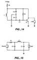
- FIG. 14illustrates the inductor of the present invention used in an oscillator circuit
- FIG. 15illustrates the inductor of the present invention used in a filter circuit.
- FIGS. 1 through 15exemplary embodiments of the present invention are shown.
- FIG. 1shows a component ring 10 of the inductor coil.
- the ring 10is almost totally enclosed except for a gap 30 .
- the gapshould offer enough distance between the two ends of the ring to avoid any problem with hillocks or other shorts forming during the manufacturing method.
- At either end of the ring 10is an area 20 for contacting the via. This is not a specially processed portion of the ring, but merely shows that the ring will be electrically connected proximate or at that point.
- the material of the ring or toroid 10is any conductive material that is compatible with the processing and other layers in which it may have some effect because of contact or proximity.
- the ring or toroidmay be made of gold, titanium, molybdenum, copper, silver, aluminum, hafnium, tin, or any alloy of these metals, may be made of a conductive oxide or nitride such as indium tin oxide, or may be formed of some other conductive material.
- the intervening insulating layers between ringsmay be formed of any compatible insulating material such as nitrides or oxides. Specific examples of such insulating materials include silicon dioxide, silicon nitride, and organic tetraethyl —oxysilane (TEOS).
- FIG. 2shows an exploded view of an inductor.
- Multiple rings 10are stacked one above another and are separated by intervening insulating or dielectric layers.
- Vias 40connect the individual rings 10 to create a good approximation to a coil structure.
- each successive ring's gapis rotated with respect to the previous ring's gap and in the same direction as one travels through the resulting coil structure.
- the ringsare connected to adjacent rings such that the vias 40 connect one side of the ring with respect to its gap to the opposite side of the adjacent ring with respect to that adjacent ring's gap.
- This structureallows current to pass along the coil structure as in a common coil inductor.
- FIG. 3shows a cut away view of a vertically oriented inductor used with a combined with an component 60 .
- the component 60is an electron source at the bottom of the coil which could provide a narrow and highly controlled beam of electrons potentially useful for electron microscopy and elemental analysis tools.
- component 60is an active detection circuit which is useable as a tuneable charged particle detector with possible uses in implanter controls and high-energy physics.
- the detectormay be implemented as a silicon PN junction.
- Airmay be the insulating material within the coil structure.
- a high permeability materialmay be placed inside the coil structure.
- An insulating fill materialmay be placed inside the coil structure.
- a conductor 40reaches through the dielectric layers 50 to act as a contact terminal.
- the coil structure formed from the interconnected rings 10generate a magnetic flux through the center of the coil structure.
- a charged particlewill be driven along by the magnetic flux lines outside the coils structure and through the coil structure to be sensed by the particle detector 60 .
- Lis the inductance
- ⁇is the permeability
- Nis the number of turns
- Ais the area of the cross section of the coil
- sis the length of the coil.
- FIG. 4shows an exploded view of a second embodiment of the inductor in which the inductor is oriented such that its longitudinal axis is in or parallel to the major plane of extension of the substrate.
- the rings 10have gaps which are offset in a rotational manner with the gaps of successive rings.
- the vias 40are really short patterned conductors on insulating or dielectric layers 50 , rather than formed through them, to connect adjoining rings 10 .
- the shape of the coil cross-sectionis limited to a square or rectangle.
- Lis the inductance
- ⁇is the permeability
- Nis the number of turns
- Ais the area of the cross section of the coil
- r 2is the outer radius
- r 1is the inner radius
- FIG. 5shows a cross sectional view of the inductor of the second embodiment.
- there must be a gap 30which is as small as possible and large enough to avoid the development of any shorts, such. as from hillocks or via like connecting conductors, across the gap 30 .
- FIG. 6shows an exposed view of the ring structure of the inductor of the present invention.
- the interconnecting viasare not shown.
- the vertical configurationoccupies a smaller area than a horizontal configuration and is more likely to be used for charged particle detection or emission.
- the horizontal configurationallows for a significantly longer coil structure than the vertical configuration since its length is not limited by the number of layers deposited.
- the thickness of individual conductive and insulating layersdepends upon the application. Current processes allow layer thicknesses as low as several Angstroms.
- the inductor of the present inventionis meant to be scalable.
- FIGS. 7A to 7 Fillustrate a horizontal inductor configuration, optimized for high coil density.
- an initial set of parallel lengths 100 of conductive materialis laid down upon an insulating layer.
- FIGS. 7C and 7Dsuccessive layers of dielectric layers are laid down and successive plugs of conductive material 110 are formed in its corresponding dielectric layer to form a ring or toroid structure.
- the cross sectional area of the inductor coilmay be made greater than it would be relying on single dielectric layer.
- the use of a single dielectric layeralthough within the scope of the present invention, limits the vertical height because there are limits to the depth in which a given through hole or via may be formed through its corresponding dielectric layer.
- a last set of conductive lengths 120formed at a slant, connect the various ring like structures to form a coil structure.
- FIGS. 8A to 8 Fillustrate a horizontal inductor configuration using only 90 degree angles.
- the initial set of conductors 100are formed with an appendage 130 to connect with an adjacent final conductor.
- the final set of conductors ad 120are formed with a similar appendage to connect neighboring rings or toroids.
- FIGS. 9A to 9 Fillustrate a horizontal inductor configuration using only 90 degree angles, with a higher coil density than the inductor of FIGS. 8A to 8 F.
- FIGS. 10A to 10 Hillustrate a horizontal inductor configuration using intermediate metal as part of a coil.
- a set of parallel conductors 100are formed on an insulating layer or substrate.
- a plug or successive plugs 110 of conductive materialare formed over their corresponding conductors 100 .
- a connection appendage 140is formed over the plug or successive plugs 110 to allow connection to form the coil structure.
- Another plug or successive plugs 110 of conductive materialare formed over the appendage 140 and underlying plugs 110 .
- a final set of parallel conductors 120are formed to connect appendages 140 and complete the coil structure.
- FIGS. 11A to 11 Fillustrate a horizontal inductor configuration showing optional core filling techniques.
- the inductance of the inductormay be increased by adding a core to the inductor.
- the formation of this deviceis similar to the device of FIGS. 7A to 7 F.
- the core 150may be formed by cutting a trench into the dielectric and capping it with a dielectric.
- the core 150may be formed of copper, gold, ferromagnetic material, or other suitable material.
- a damascene process for encapsulating the core materialmay be used so as to prevent migration of the core material to other component parts and impairing device function.
- FIG.12illustrates a pair of interdigitated or intertwined inductor coil 200 and 210 for inductively coupled networks.
- FIG. 13illustrates an inductor coil 220 in which two levels of metallization are formed in a slanting manner.
- FIG. 14shows an inductor of the present invention used in an oscillator circuit which generates a sine wave and has inductive-capacitive feedback.
- FIG. 15shows an inductor used in a filter circuit.
- the present inventionmay also be used in microelectromechanical devices.
- One possible applicationconcerns the use of the inductor with a filled core of the present invention to control an array of mechanically deformed micromirrors. Instead of electrostatic control, magnetic forces could be used to control microdevices.
- Any processmay be used, such as CVD, MBE, or ALD, as long as it provides a smooth conformal conductive film on an insulating layer having a via formed therein.
- the ringsmay be patterned by laser trimming.
- the component layersmay also be formed in one location and then transferred to the desired substrate.
- the chosen processonly needs to provide good planarity and step coverage as well as chemical compatibility and adhesion with contacting component layers.
- the processincludes forming through holes in an insulating layer to a semiconducting or insulating substrate and depositing the various layers of semiconductor, insulating, and conductive material using the deposition techniques to provide a conformal film that exhibits good step coverage.
- CMPChemical mechanical polishing
- a slurry with silicon or other granular componentis deposited on the layer to be polished.
- the granular componentsare about 0.2 microns in diameter.
- a padis used to press upon and move around the slurry. The pad may rotate, the substrate may rotate, or both the pad and the substrate may rotate.
- a substrateis chosen.
- Several underlying layersmay first be deposited and patterned to form conductor paths and various component layers.
- an insulating filmmay be deposited and may also be patterned to include a via for each inductor to be formed.
- the viais thereafter filled with a conductive material.
- a first metal or other conductive layeris then deposited over the via.
- a maskmay be used to form a metal or conductor pattern or the pattern may be developed through etching, laser trimming, or other cut and remove process to form a ring or toroid shape which has a gap formed near the via in which the via electrically connects the ring or toroid. Any conductive material in the ring or toroid may be removed.
- conductive materialmay be retained within the ring or toroid and electrically insulated from it. Then, a dielectric or insulating layer is deposited over the ring or toroid. A through hole is formed in the insulating layer over the unconnected end of the ring or toroid immediately underneath. The through hole is filled with a conductive material. Another conductive layer is formed over the insulating layer. It is patterned in a similar manner to the first metal or conductive layer. The difference is that the gap of the second ring or toroid is rotated at an angle from the gap of the first ring or toroid. The end of the first ring or toroid is connected not to the corresponding end of the second ring or toroid, but to the opposing end of the ring or toroid. By building successive layers in this manner, a coil structure is created as long as the gap of the successive ring or toroid is rotated in the same direction as done in underlying layers.
- a substrateis chosen.
- Several underlying layersmay first be deposited and patterned to form conductor paths and various component layers.
- a metal layeris deposited by a masking or later pattern so that there are parallel conductor lengths equal in number to the desired number of rings or toroids in the coil structure.
- the spacing between and thickness of the rings or toroidsmay also be set as desired. It may be that a gap location is to be formed in this first layer.
- the materialis removed by etching, trimming, or other cutting and removing process to establish a gap which will effectively appear to rotate in a cross section view of the coil structure going from successive rings or toroids.
- conductorsmay be formed to electrically connect the rings or toroids which need to be connected at this level.
- the next layers depositedare a dielectric layer to serve at least as an inner area of the ring or toroid to be formed as well as relatively small strips of metal or conductive material. These strips are the length of the thickness of the toroid, measured by subtracting the inner radius from the outer radius. If a gap is to be formed, the affected ring or toroid has no metal or conductive material placed at the gap location and is filled there with the dielectric material. This may be accomplished by either not forming metal or conductive material at the gap or later removing such material.
Landscapes
- Engineering & Computer Science (AREA)
- Power Engineering (AREA)
- Microelectronics & Electronic Packaging (AREA)
- Physics & Mathematics (AREA)
- Condensed Matter Physics & Semiconductors (AREA)
- General Physics & Mathematics (AREA)
- Computer Hardware Design (AREA)
- Manufacturing & Machinery (AREA)
- Semiconductor Integrated Circuits (AREA)
- Coils Or Transformers For Communication (AREA)
Abstract
Description
Claims (43)
Priority Applications (2)
| Application Number | Priority Date | Filing Date | Title |
|---|---|---|---|
| US10/013,572US6614093B2 (en) | 2001-12-11 | 2001-12-11 | Integrated inductor in semiconductor manufacturing |
| US10/463,158US20040212038A1 (en) | 2001-12-11 | 2003-06-16 | Integrated inductor in semiconductor manufacturing |
Applications Claiming Priority (1)
| Application Number | Priority Date | Filing Date | Title |
|---|---|---|---|
| US10/013,572US6614093B2 (en) | 2001-12-11 | 2001-12-11 | Integrated inductor in semiconductor manufacturing |
Related Child Applications (1)
| Application Number | Title | Priority Date | Filing Date |
|---|---|---|---|
| US10/463,158DivisionUS20040212038A1 (en) | 2001-12-11 | 2003-06-16 | Integrated inductor in semiconductor manufacturing |
Publications (2)
| Publication Number | Publication Date |
|---|---|
| US20030109118A1 US20030109118A1 (en) | 2003-06-12 |
| US6614093B2true US6614093B2 (en) | 2003-09-02 |
Family
ID=21760621
Family Applications (2)
| Application Number | Title | Priority Date | Filing Date |
|---|---|---|---|
| US10/013,572Expired - LifetimeUS6614093B2 (en) | 2001-12-11 | 2001-12-11 | Integrated inductor in semiconductor manufacturing |
| US10/463,158AbandonedUS20040212038A1 (en) | 2001-12-11 | 2003-06-16 | Integrated inductor in semiconductor manufacturing |
Family Applications After (1)
| Application Number | Title | Priority Date | Filing Date |
|---|---|---|---|
| US10/463,158AbandonedUS20040212038A1 (en) | 2001-12-11 | 2003-06-16 | Integrated inductor in semiconductor manufacturing |
Country Status (1)
| Country | Link |
|---|---|
| US (2) | US6614093B2 (en) |
Cited By (24)
| Publication number | Priority date | Publication date | Assignee | Title |
|---|---|---|---|---|
| US20020095770A1 (en)* | 1999-07-09 | 2002-07-25 | Micron Technology, Inc. | Integrated circuit inductors |
| US20040036099A1 (en)* | 2002-08-22 | 2004-02-26 | Er-Xuan Ping | Dual-sided capacitor and method of formation |
| US20050174208A1 (en)* | 2002-09-30 | 2005-08-11 | Tdk Corporation | Inductive element and manufacturing method of the same |
| US20060040628A1 (en)* | 2004-08-20 | 2006-02-23 | Alain-Serge Porret | Television receiver including an integrated band selection filter |
| US7229908B1 (en) | 2004-06-04 | 2007-06-12 | National Semiconductor Corporation | System and method for manufacturing an out of plane integrated circuit inductor |
| US20070280246A1 (en)* | 2006-05-31 | 2007-12-06 | Berkman William H | System and Method for Communicating in a Multi-Unit Structure |
| US20080061916A1 (en)* | 2006-03-20 | 2008-03-13 | United State Government As Represented By Secretary Of The Army | Lateral Piezoelectric Driven Highly Tunable Micro-electromechanical System (MEMS) Inductor |
| US7474189B1 (en) | 2005-03-24 | 2009-01-06 | Rf Micro Devices, Inc. | Circuit board embedded inductor |
| US20090188104A1 (en)* | 2008-01-25 | 2009-07-30 | Taiwan Semiconductor Manufacturing Co., Ltd. | Method of Manufacturing a Coil Inductor |
| US20100295183A1 (en)* | 2009-05-20 | 2010-11-25 | Gurtej Sandhu | Method for providing electrical connections to spaced conductive lines |
| US20110127872A1 (en)* | 2008-05-05 | 2011-06-02 | Marcus Podack | Coil For An Electric Machine And Method For Producing A Coil |
| KR101062545B1 (en) | 2005-03-30 | 2011-09-06 | 인텔 코포레이션 | Apparatus, Systems, and Methods for CMOS Integrated Circuit Devices |
| US8068004B1 (en)* | 2010-02-03 | 2011-11-29 | Xilinx, Inc. | Embedded inductor |
| US20120104103A1 (en)* | 2010-10-29 | 2012-05-03 | Nxp B.V. | Integrated pcb uhf rfid matching network/antenna |
| US20120188039A1 (en)* | 2005-07-22 | 2012-07-26 | Winstead Assets Limited | Field winding |
| US8742539B2 (en)* | 2012-07-27 | 2014-06-03 | Infineon Technologies Austria Ag | Semiconductor component and method for producing a semiconductor component |
| US8823133B2 (en) | 2011-03-29 | 2014-09-02 | Xilinx, Inc. | Interposer having an inductor |
| US20150279921A1 (en)* | 2014-03-26 | 2015-10-01 | Wafertech, Llc | Inductor structures for integrated circuits |
| US20160005530A1 (en)* | 2014-07-02 | 2016-01-07 | Analog Devices Global | Inductive component for use in an integrated circuit, a transformer and an inductor formed as part of an integrated circuit |
| US9330823B1 (en) | 2011-12-19 | 2016-05-03 | Xilinx, Inc. | Integrated circuit structure with inductor in silicon interposer |
| US9337138B1 (en) | 2012-03-09 | 2016-05-10 | Xilinx, Inc. | Capacitors within an interposer coupled to supply and ground planes of a substrate |
| US9406738B2 (en) | 2011-07-20 | 2016-08-02 | Xilinx, Inc. | Inductive structure formed using through silicon vias |
| US10381720B2 (en) | 2010-12-08 | 2019-08-13 | Nxp B.V. | Radio frequency identification (RFID) integrated circuit (IC) and matching network/antenna embedded in surface mount devices (SMD) |
| US11404197B2 (en) | 2017-06-09 | 2022-08-02 | Analog Devices Global Unlimited Company | Via for magnetic core of inductive component |
Families Citing this family (17)
| Publication number | Priority date | Publication date | Assignee | Title |
|---|---|---|---|---|
| US6688169B2 (en)* | 2001-06-15 | 2004-02-10 | Textron Systems Corporation | Systems and methods for sensing an acoustic signal using microelectromechanical systems technology |
| TW558835B (en)* | 2002-10-01 | 2003-10-21 | Asia Pacific Microsystems Inc | High-frequency inductance adjustment method for passive device |
| DE102005014929B4 (en)* | 2005-04-01 | 2008-04-17 | Newlogic Technologies Gmbh | Integrated coil and integrated transformer |
| US7776705B2 (en)* | 2006-09-06 | 2010-08-17 | Atmel Corporation | Method for fabricating a thick copper line and copper inductor resulting therefrom |
| US8327523B2 (en)* | 2006-11-28 | 2012-12-11 | Semiconductor Components Industries, Llc | High density planarized inductor and method of making the same |
| FR2909482A1 (en)* | 2006-12-01 | 2008-06-06 | Commissariat Energie Atomique | OPTIMIZED SOLENOID WINDING |
| KR100977685B1 (en)* | 2008-02-19 | 2010-08-24 | 한국과학기술원 | Variable Inductor Using Micro Electromechanical System and Its Applications |
| US7763976B2 (en)* | 2008-09-30 | 2010-07-27 | Freescale Semiconductor, Inc. | Integrated circuit module with integrated passive device |
| US8313659B2 (en)* | 2009-07-10 | 2012-11-20 | Seagate Technology Llc | Fabrication of multi-dimensional microstructures |
| US12224096B2 (en) | 2013-03-15 | 2025-02-11 | Qorvo Us, Inc. | Advanced 3D inductor structures with confined magnetic field |
| US9899133B2 (en) | 2013-08-01 | 2018-02-20 | Qorvo Us, Inc. | Advanced 3D inductor structures with confined magnetic field |
| US10062494B2 (en)* | 2014-11-03 | 2018-08-28 | Qorvo Us, Inc. | Apparatus with 3D inductors |
| WO2017075101A1 (en)* | 2015-10-26 | 2017-05-04 | NuVolta Technologies | Magnetic structures with self-enclosed magnetic paths |
| US10692645B2 (en)* | 2016-03-23 | 2020-06-23 | Qorvo Us, Inc. | Coupled inductor structures |
| CN110459535B (en)* | 2019-07-22 | 2021-03-09 | 福建省福联集成电路有限公司 | A manufacturing method of a laminated inductor and a device made therefrom |
| KR102649010B1 (en)* | 2020-03-05 | 2024-03-20 | 한국전자통신연구원 | Radio frequency weak magnetic field detection sensor and manufacturing method of the same |
| CN115308899B (en)* | 2022-08-29 | 2024-09-24 | 觉芯电子(无锡)有限公司 | Electromagnetic driving micro-mirror device with high-density coil and preparation process |
Citations (17)
| Publication number | Priority date | Publication date | Assignee | Title |
|---|---|---|---|---|
| US4313152A (en)* | 1979-01-12 | 1982-01-26 | U.S. Philips Corporation | Flat electric coil |
| DE3346659A1 (en)* | 1983-12-23 | 1985-07-04 | Standard Elektrik Lorenz Ag, 7000 Stuttgart | Inductive component |
| JPS61179562A (en)* | 1985-02-04 | 1986-08-12 | Nec Corp | Solid type inductance |
| JPH0269971A (en)* | 1988-09-05 | 1990-03-08 | Seiko Epson Corp | Semiconductor device with built-in inductance |
| JPH03178158A (en)* | 1989-12-06 | 1991-08-02 | Sharp Corp | Semiconductor device |
| JPH04348558A (en)* | 1991-05-27 | 1992-12-03 | Nec Corp | Semiconductor device |
| JPH0621347A (en)* | 1992-07-01 | 1994-01-28 | Seiko Epson Corp | Semiconductor device |
| US5336921A (en)* | 1992-01-27 | 1994-08-09 | Motorola, Inc. | Vertical trench inductor |
| US5610433A (en)* | 1995-03-13 | 1997-03-11 | National Semiconductor Corporation | Multi-turn, multi-level IC inductor with crossovers |
| US5612660A (en)* | 1994-07-27 | 1997-03-18 | Canon Kabushiki Kaisha | Inductance element |
| US5831331A (en)* | 1996-11-22 | 1998-11-03 | Philips Electronics North America Corporation | Self-shielding inductor for multi-layer semiconductor integrated circuits |
| US5884990A (en)* | 1996-08-23 | 1999-03-23 | International Business Machines Corporation | Integrated circuit inductor |
| US6008102A (en)* | 1998-04-09 | 1999-12-28 | Motorola, Inc. | Method of forming a three-dimensional integrated inductor |
| US6037649A (en)* | 1999-04-01 | 2000-03-14 | Winbond Electronics Corp. | Three-dimension inductor structure in integrated circuit technology |
| US6240622B1 (en)* | 1999-07-09 | 2001-06-05 | Micron Technology, Inc. | Integrated circuit inductors |
| US6291872B1 (en)* | 1999-11-04 | 2001-09-18 | Taiwan Semiconductor Manufacturing Co., Ltd. | Three-dimensional type inductor for mixed mode radio frequency device |
| US6376895B2 (en)* | 1998-04-29 | 2002-04-23 | Micron Technology, Inc. | High-Q inductive elements |
Family Cites Families (3)
| Publication number | Priority date | Publication date | Assignee | Title |
|---|---|---|---|---|
| JPH0377360A (en)* | 1989-08-18 | 1991-04-02 | Mitsubishi Electric Corp | semiconductor equipment |
| US6060383A (en)* | 1998-08-10 | 2000-05-09 | Nogami; Takeshi | Method for making multilayered coaxial interconnect structure |
| US6392524B1 (en)* | 2000-06-09 | 2002-05-21 | Xerox Corporation | Photolithographically-patterned out-of-plane coil structures and method of making |
- 2001
- 2001-12-11USUS10/013,572patent/US6614093B2/ennot_activeExpired - Lifetime
- 2003
- 2003-06-16USUS10/463,158patent/US20040212038A1/ennot_activeAbandoned
Patent Citations (17)
| Publication number | Priority date | Publication date | Assignee | Title |
|---|---|---|---|---|
| US4313152A (en)* | 1979-01-12 | 1982-01-26 | U.S. Philips Corporation | Flat electric coil |
| DE3346659A1 (en)* | 1983-12-23 | 1985-07-04 | Standard Elektrik Lorenz Ag, 7000 Stuttgart | Inductive component |
| JPS61179562A (en)* | 1985-02-04 | 1986-08-12 | Nec Corp | Solid type inductance |
| JPH0269971A (en)* | 1988-09-05 | 1990-03-08 | Seiko Epson Corp | Semiconductor device with built-in inductance |
| JPH03178158A (en)* | 1989-12-06 | 1991-08-02 | Sharp Corp | Semiconductor device |
| JPH04348558A (en)* | 1991-05-27 | 1992-12-03 | Nec Corp | Semiconductor device |
| US5336921A (en)* | 1992-01-27 | 1994-08-09 | Motorola, Inc. | Vertical trench inductor |
| JPH0621347A (en)* | 1992-07-01 | 1994-01-28 | Seiko Epson Corp | Semiconductor device |
| US5612660A (en)* | 1994-07-27 | 1997-03-18 | Canon Kabushiki Kaisha | Inductance element |
| US5610433A (en)* | 1995-03-13 | 1997-03-11 | National Semiconductor Corporation | Multi-turn, multi-level IC inductor with crossovers |
| US5884990A (en)* | 1996-08-23 | 1999-03-23 | International Business Machines Corporation | Integrated circuit inductor |
| US5831331A (en)* | 1996-11-22 | 1998-11-03 | Philips Electronics North America Corporation | Self-shielding inductor for multi-layer semiconductor integrated circuits |
| US6008102A (en)* | 1998-04-09 | 1999-12-28 | Motorola, Inc. | Method of forming a three-dimensional integrated inductor |
| US6376895B2 (en)* | 1998-04-29 | 2002-04-23 | Micron Technology, Inc. | High-Q inductive elements |
| US6037649A (en)* | 1999-04-01 | 2000-03-14 | Winbond Electronics Corp. | Three-dimension inductor structure in integrated circuit technology |
| US6240622B1 (en)* | 1999-07-09 | 2001-06-05 | Micron Technology, Inc. | Integrated circuit inductors |
| US6291872B1 (en)* | 1999-11-04 | 2001-09-18 | Taiwan Semiconductor Manufacturing Co., Ltd. | Three-dimensional type inductor for mixed mode radio frequency device |
Cited By (50)
| Publication number | Priority date | Publication date | Assignee | Title |
|---|---|---|---|---|
| US20050122199A1 (en)* | 1999-07-09 | 2005-06-09 | Micron Technology, Inc. | Integrated circuit inductors |
| US20020095770A1 (en)* | 1999-07-09 | 2002-07-25 | Micron Technology, Inc. | Integrated circuit inductors |
| US7388462B2 (en)* | 1999-07-09 | 2008-06-17 | Micron Technology, Inc. | Integrated circuit inductors |
| US7355232B2 (en) | 2002-08-22 | 2008-04-08 | Micron Technology, Inc. | Memory devices with dual-sided capacitors |
| US20040036099A1 (en)* | 2002-08-22 | 2004-02-26 | Er-Xuan Ping | Dual-sided capacitor and method of formation |
| US20040264102A1 (en)* | 2002-08-22 | 2004-12-30 | Er-Xuan Ping | Dual-sided capacitor and method of formation |
| US6858493B2 (en)* | 2002-08-22 | 2005-02-22 | Micron Technology, Inc. | Method of forming a dual-sided capacitor |
| US20060001052A1 (en)* | 2002-08-22 | 2006-01-05 | Er-Xuan Ping | Dual-sided capacitor and method of formation |
| US7071056B2 (en) | 2002-08-22 | 2006-07-04 | Micron Technology, Inc. | Method of forming a dual-sided capacitor |
| US20050174208A1 (en)* | 2002-09-30 | 2005-08-11 | Tdk Corporation | Inductive element and manufacturing method of the same |
| US7212095B2 (en)* | 2002-09-30 | 2007-05-01 | Tdk Corporation | Inductive element and manufacturing method of the same |
| US7229908B1 (en) | 2004-06-04 | 2007-06-12 | National Semiconductor Corporation | System and method for manufacturing an out of plane integrated circuit inductor |
| US20060040628A1 (en)* | 2004-08-20 | 2006-02-23 | Alain-Serge Porret | Television receiver including an integrated band selection filter |
| US7251466B2 (en) | 2004-08-20 | 2007-07-31 | Xceive Corporation | Television receiver including an integrated band selection filter |
| US7474189B1 (en) | 2005-03-24 | 2009-01-06 | Rf Micro Devices, Inc. | Circuit board embedded inductor |
| KR101062545B1 (en) | 2005-03-30 | 2011-09-06 | 인텔 코포레이션 | Apparatus, Systems, and Methods for CMOS Integrated Circuit Devices |
| US9361567B2 (en)* | 2005-07-22 | 2016-06-07 | Winstead Assets Limited | Inductor |
| US20120188039A1 (en)* | 2005-07-22 | 2012-07-26 | Winstead Assets Limited | Field winding |
| US20140319227A1 (en)* | 2005-07-22 | 2014-10-30 | Winstead Assets Limited | Inductor |
| US7486002B2 (en)* | 2006-03-20 | 2009-02-03 | The United States Of America As Represented By The Secretary Of The Army | Lateral piezoelectric driven highly tunable micro-electromechanical system (MEMS) inductor |
| US20080061916A1 (en)* | 2006-03-20 | 2008-03-13 | United State Government As Represented By Secretary Of The Army | Lateral Piezoelectric Driven Highly Tunable Micro-electromechanical System (MEMS) Inductor |
| US7596079B2 (en)* | 2006-05-31 | 2009-09-29 | Current Technologies, Llc | System and method for communicating in a multi-unit structure |
| US20070280246A1 (en)* | 2006-05-31 | 2007-12-06 | Berkman William H | System and Method for Communicating in a Multi-Unit Structure |
| US7666688B2 (en)* | 2008-01-25 | 2010-02-23 | Taiwan Semiconductor Manufacturing Co., Ltd. | Method of manufacturing a coil inductor |
| TWI394186B (en)* | 2008-01-25 | 2013-04-21 | Taiwan Semiconductor Mfg | A method of manufacturing a coil inductor |
| US20090188104A1 (en)* | 2008-01-25 | 2009-07-30 | Taiwan Semiconductor Manufacturing Co., Ltd. | Method of Manufacturing a Coil Inductor |
| US20110127872A1 (en)* | 2008-05-05 | 2011-06-02 | Marcus Podack | Coil For An Electric Machine And Method For Producing A Coil |
| US9035523B2 (en)* | 2008-05-05 | 2015-05-19 | Brose Fahrzeugteile Gmbh & Co. Kg, Würzburg | Coil for an electric machine and method for producing a coil |
| US8043964B2 (en)* | 2009-05-20 | 2011-10-25 | Micron Technology, Inc. | Method for providing electrical connections to spaced conductive lines |
| US20100295183A1 (en)* | 2009-05-20 | 2010-11-25 | Gurtej Sandhu | Method for providing electrical connections to spaced conductive lines |
| US8629051B2 (en) | 2009-05-20 | 2014-01-14 | Micron Technology, Inc. | Method for providing electrical connections to spaced conductive lines |
| US8735285B2 (en) | 2009-05-20 | 2014-05-27 | Micron Technology, Inc. | Method for providing electrical connections to spaced conductive lines |
| US8987906B2 (en) | 2009-05-20 | 2015-03-24 | Micron Technology, Inc. | Method for providing electrical connections to spaced conductive lines |
| US8383504B2 (en) | 2009-05-20 | 2013-02-26 | Micron Technology, Inc. | Method for providing electrical connections to spaced conductive lines |
| US9224742B2 (en) | 2009-05-20 | 2015-12-29 | Micron Technology, Inc. | Method for providing electrical connections to spaced conductive lines |
| US8068004B1 (en)* | 2010-02-03 | 2011-11-29 | Xilinx, Inc. | Embedded inductor |
| US20120104103A1 (en)* | 2010-10-29 | 2012-05-03 | Nxp B.V. | Integrated pcb uhf rfid matching network/antenna |
| US10381720B2 (en) | 2010-12-08 | 2019-08-13 | Nxp B.V. | Radio frequency identification (RFID) integrated circuit (IC) and matching network/antenna embedded in surface mount devices (SMD) |
| US8823133B2 (en) | 2011-03-29 | 2014-09-02 | Xilinx, Inc. | Interposer having an inductor |
| US9406738B2 (en) | 2011-07-20 | 2016-08-02 | Xilinx, Inc. | Inductive structure formed using through silicon vias |
| US9330823B1 (en) | 2011-12-19 | 2016-05-03 | Xilinx, Inc. | Integrated circuit structure with inductor in silicon interposer |
| US9337138B1 (en) | 2012-03-09 | 2016-05-10 | Xilinx, Inc. | Capacitors within an interposer coupled to supply and ground planes of a substrate |
| DE102013214649B4 (en)* | 2012-07-27 | 2019-02-14 | Infineon Technologies Austria Ag | SEMICONDUCTOR COMPONENT WITH COIL AND METHOD FOR PRODUCING A SEMICONDUCTOR COMPONENT WITH COIL |
| US8742539B2 (en)* | 2012-07-27 | 2014-06-03 | Infineon Technologies Austria Ag | Semiconductor component and method for producing a semiconductor component |
| US20150279921A1 (en)* | 2014-03-26 | 2015-10-01 | Wafertech, Llc | Inductor structures for integrated circuits |
| US10128325B2 (en)* | 2014-03-26 | 2018-11-13 | Wafertech, Llc | Inductor structures for integrated circuits |
| CN105244344A (en)* | 2014-07-02 | 2016-01-13 | 亚德诺半导体集团 | An inductive component for use in an integrated circuit, a transformer and an inductor formed as part of an integrated circuit |
| US20160005530A1 (en)* | 2014-07-02 | 2016-01-07 | Analog Devices Global | Inductive component for use in an integrated circuit, a transformer and an inductor formed as part of an integrated circuit |
| CN105244344B (en)* | 2014-07-02 | 2018-12-25 | 亚德诺半导体集团 | Used in the Inductive component of integrated circuit, segment set is formed into the transformer and inductor of circuit |
| US11404197B2 (en) | 2017-06-09 | 2022-08-02 | Analog Devices Global Unlimited Company | Via for magnetic core of inductive component |
Also Published As
| Publication number | Publication date |
|---|---|
| US20030109118A1 (en) | 2003-06-12 |
| US20040212038A1 (en) | 2004-10-28 |
Similar Documents
| Publication | Publication Date | Title |
|---|---|---|
| US6614093B2 (en) | Integrated inductor in semiconductor manufacturing | |
| US11502161B2 (en) | Metal insulator metal capacitor structure having high capacitance | |
| JP4549002B2 (en) | Electronic component having electrically conductive connection made of carbon nanotube and method for manufacturing the same | |
| JPH08250332A (en) | Three-dimensional integrated circuit inductor | |
| US9472504B2 (en) | Semiconductor having a high aspect ratio via | |
| US8174355B2 (en) | Semiconductor device and method for manufacturing the same | |
| KR100803489B1 (en) | Semiconductor integrated circuit and semiconductor device manufacturing method | |
| CN103247596A (en) | On-chip ferrite bead inductor | |
| TWI292204B (en) | Semiconductor device and method for manufacturing the same | |
| CN102420210A (en) | Device with through-silicon via (tsv) and method of forming the same | |
| JPH09162354A (en) | Integrated inductor structure and its manufacture | |
| TW202116114A (en) | Equipment and methods for plasma processing | |
| WO2021080690A1 (en) | Methods for etching metal films using plasma processing | |
| CN109585425A (en) | Semiconductor structure and its manufacturing method | |
| TW478135B (en) | Lateral high-q inductor for semiconductor devices | |
| CN112928095B (en) | Interconnection structure, preparation method thereof and semiconductor structure | |
| CN119314948B (en) | Semiconductor structure preparation method and semiconductor structure | |
| CN1141738C (en) | Method for manufacturing on-chip inductor assembly | |
| KR20010050952A (en) | Method of manufacturing lateral high-q inductor for semiconductor devices | |
| US20030122175A1 (en) | Integrated passive devices formed by demascene processing | |
| US6784045B1 (en) | Microchannel formation for fuses, interconnects, capacitors, and inductors | |
| KR100737155B1 (en) | Method for manufacturing high frequency inductor of semiconductor device | |
| US11548779B2 (en) | Capacitive micro structure | |
| KR100575872B1 (en) | Manufacturing Method Of Semiconductor Inductor | |
| TW202242926A (en) | Inductor structure and manufacturing method for the same |
Legal Events
| Date | Code | Title | Description |
|---|---|---|---|
| AS | Assignment | Owner name:LSI LOGIC CORPORATION, CALIFORNIA Free format text:ASSIGNMENT OF ASSIGNORS INTEREST;ASSIGNORS:OTT, GEORGE;VON THUN, MATTHEW;COLE, RICHARD;REEL/FRAME:012380/0250 Effective date:20011207 | |
| STCF | Information on status: patent grant | Free format text:PATENTED CASE | |
| FPAY | Fee payment | Year of fee payment:4 | |
| FEPP | Fee payment procedure | Free format text:PAYOR NUMBER ASSIGNED (ORIGINAL EVENT CODE: ASPN); ENTITY STATUS OF PATENT OWNER: LARGE ENTITY | |
| FPAY | Fee payment | Year of fee payment:8 | |
| AS | Assignment | Owner name:DEUTSCHE BANK AG NEW YORK BRANCH, AS COLLATERAL AG Free format text:PATENT SECURITY AGREEMENT;ASSIGNORS:LSI CORPORATION;AGERE SYSTEMS LLC;REEL/FRAME:032856/0031 Effective date:20140506 | |
| AS | Assignment | Owner name:LSI CORPORATION, CALIFORNIA Free format text:CHANGE OF NAME;ASSIGNOR:LSI LOGIC CORPORATION;REEL/FRAME:033102/0270 Effective date:20070406 | |
| FPAY | Fee payment | Year of fee payment:12 | |
| AS | Assignment | Owner name:AVAGO TECHNOLOGIES GENERAL IP (SINGAPORE) PTE. LTD Free format text:ASSIGNMENT OF ASSIGNORS INTEREST;ASSIGNOR:LSI CORPORATION;REEL/FRAME:035390/0388 Effective date:20140814 | |
| AS | Assignment | Owner name:AGERE SYSTEMS LLC, PENNSYLVANIA Free format text:TERMINATION AND RELEASE OF SECURITY INTEREST IN PATENT RIGHTS (RELEASES RF 032856-0031);ASSIGNOR:DEUTSCHE BANK AG NEW YORK BRANCH, AS COLLATERAL AGENT;REEL/FRAME:037684/0039 Effective date:20160201 Owner name:LSI CORPORATION, CALIFORNIA Free format text:TERMINATION AND RELEASE OF SECURITY INTEREST IN PATENT RIGHTS (RELEASES RF 032856-0031);ASSIGNOR:DEUTSCHE BANK AG NEW YORK BRANCH, AS COLLATERAL AGENT;REEL/FRAME:037684/0039 Effective date:20160201 | |
| AS | Assignment | Owner name:BANK OF AMERICA, N.A., AS COLLATERAL AGENT, NORTH CAROLINA Free format text:PATENT SECURITY AGREEMENT;ASSIGNOR:AVAGO TECHNOLOGIES GENERAL IP (SINGAPORE) PTE. LTD.;REEL/FRAME:037808/0001 Effective date:20160201 Owner name:BANK OF AMERICA, N.A., AS COLLATERAL AGENT, NORTH Free format text:PATENT SECURITY AGREEMENT;ASSIGNOR:AVAGO TECHNOLOGIES GENERAL IP (SINGAPORE) PTE. LTD.;REEL/FRAME:037808/0001 Effective date:20160201 | |
| AS | Assignment | Owner name:AVAGO TECHNOLOGIES GENERAL IP (SINGAPORE) PTE. LTD., SINGAPORE Free format text:TERMINATION AND RELEASE OF SECURITY INTEREST IN PATENTS;ASSIGNOR:BANK OF AMERICA, N.A., AS COLLATERAL AGENT;REEL/FRAME:041710/0001 Effective date:20170119 Owner name:AVAGO TECHNOLOGIES GENERAL IP (SINGAPORE) PTE. LTD Free format text:TERMINATION AND RELEASE OF SECURITY INTEREST IN PATENTS;ASSIGNOR:BANK OF AMERICA, N.A., AS COLLATERAL AGENT;REEL/FRAME:041710/0001 Effective date:20170119 | |
| AS | Assignment | Owner name:BELL SEMICONDUCTOR, LLC, ILLINOIS Free format text:ASSIGNMENT OF ASSIGNORS INTEREST;ASSIGNORS:AVAGO TECHNOLOGIES GENERAL IP (SINGAPORE) PTE. LTD.;BROADCOM CORPORATION;REEL/FRAME:044886/0001 Effective date:20171208 | |
| AS | Assignment | Owner name:CORTLAND CAPITAL MARKET SERVICES LLC, AS COLLATERA Free format text:SECURITY INTEREST;ASSIGNORS:HILCO PATENT ACQUISITION 56, LLC;BELL SEMICONDUCTOR, LLC;BELL NORTHERN RESEARCH, LLC;REEL/FRAME:045216/0020 Effective date:20180124 | |
| AS | Assignment | Owner name:BELL NORTHERN RESEARCH, LLC, ILLINOIS Free format text:SECURITY INTEREST;ASSIGNOR:CORTLAND CAPITAL MARKET SERVICES LLC;REEL/FRAME:060885/0001 Effective date:20220401 Owner name:BELL SEMICONDUCTOR, LLC, ILLINOIS Free format text:SECURITY INTEREST;ASSIGNOR:CORTLAND CAPITAL MARKET SERVICES LLC;REEL/FRAME:060885/0001 Effective date:20220401 Owner name:HILCO PATENT ACQUISITION 56, LLC, ILLINOIS Free format text:SECURITY INTEREST;ASSIGNOR:CORTLAND CAPITAL MARKET SERVICES LLC;REEL/FRAME:060885/0001 Effective date:20220401 |