US6613632B2 - Fabrication method for a silicon nitride read-only memory - Google Patents
Fabrication method for a silicon nitride read-only memoryDownload PDFInfo
- Publication number
- US6613632B2 US6613632B2US10/158,260US15826002AUS6613632B2US 6613632 B2US6613632 B2US 6613632B2US 15826002 AUS15826002 AUS 15826002AUS 6613632 B2US6613632 B2US 6613632B2
- Authority
- US
- United States
- Prior art keywords
- oxide layer
- layer
- silicon nitride
- substrate
- angstroms
- Prior art date
- Legal status (The legal status is an assumption and is not a legal conclusion. Google has not performed a legal analysis and makes no representation as to the accuracy of the status listed.)
- Expired - Lifetime
Links
- 229910052581Si3N4Inorganic materials0.000titleclaimsabstractdescription50
- HQVNEWCFYHHQES-UHFFFAOYSA-Nsilicon nitrideChemical compoundN12[Si]34N5[Si]62N3[Si]51N64HQVNEWCFYHHQES-UHFFFAOYSA-N0.000titleclaimsabstractdescription48
- 238000000034methodMethods0.000titleclaimsabstractdescription44
- 238000004519manufacturing processMethods0.000titleabstractdescription20
- 239000000758substrateSubstances0.000claimsabstractdescription31
- 230000003647oxidationEffects0.000claimsabstractdescription11
- 238000007254oxidation reactionMethods0.000claimsabstractdescription11
- 238000009279wet oxidation reactionMethods0.000claimsdescription11
- IJGRMHOSHXDMSA-UHFFFAOYSA-NAtomic nitrogenChemical compoundN#NIJGRMHOSHXDMSA-UHFFFAOYSA-N0.000claimsdescription6
- UFHFLCQGNIYNRP-UHFFFAOYSA-NHydrogenChemical compound[H][H]UFHFLCQGNIYNRP-UHFFFAOYSA-N0.000claimsdescription3
- QVGXLLKOCUKJST-UHFFFAOYSA-Natomic oxygenChemical compound[O]QVGXLLKOCUKJST-UHFFFAOYSA-N0.000claimsdescription3
- 239000001257hydrogenSubstances0.000claimsdescription3
- 229910052739hydrogenInorganic materials0.000claimsdescription3
- 229910052757nitrogenInorganic materials0.000claimsdescription3
- 239000001301oxygenSubstances0.000claimsdescription3
- 229910052760oxygenInorganic materials0.000claimsdescription3
- 238000000059patterningMethods0.000claimsdescription3
- 239000000463materialSubstances0.000claims8
- 230000000717retained effectEffects0.000claims1
- 229910052814silicon oxideInorganic materials0.000description7
- 229910021420polycrystalline siliconInorganic materials0.000description6
- 229920005591polysiliconPolymers0.000description6
- VYPSYNLAJGMNEJ-UHFFFAOYSA-NSilicium dioxideChemical compoundO=[Si]=OVYPSYNLAJGMNEJ-UHFFFAOYSA-N0.000description5
- 230000008901benefitEffects0.000description4
- 230000015572biosynthetic processEffects0.000description3
- XUIMIQQOPSSXEZ-UHFFFAOYSA-NSiliconChemical compound[Si]XUIMIQQOPSSXEZ-UHFFFAOYSA-N0.000description2
- 230000007547defectEffects0.000description2
- 150000002500ionsChemical class0.000description2
- 238000012986modificationMethods0.000description2
- 230000004048modificationEffects0.000description2
- 238000012545processingMethods0.000description2
- 229910052710siliconInorganic materials0.000description2
- 239000010703siliconSubstances0.000description2
- 230000002411adverseEffects0.000description1
- 238000013459approachMethods0.000description1
- 238000005229chemical vapour depositionMethods0.000description1
- 238000011161developmentMethods0.000description1
- 230000006870functionEffects0.000description1
- 230000035945sensitivityEffects0.000description1
- 238000003860storageMethods0.000description1
Images


Classifications
- H—ELECTRICITY
- H10—SEMICONDUCTOR DEVICES; ELECTRIC SOLID-STATE DEVICES NOT OTHERWISE PROVIDED FOR
- H10B—ELECTRONIC MEMORY DEVICES
- H10B43/00—EEPROM devices comprising charge-trapping gate insulators
- H10B43/30—EEPROM devices comprising charge-trapping gate insulators characterised by the memory core region
- H—ELECTRICITY
- H10—SEMICONDUCTOR DEVICES; ELECTRIC SOLID-STATE DEVICES NOT OTHERWISE PROVIDED FOR
- H10B—ELECTRONIC MEMORY DEVICES
- H10B69/00—Erasable-and-programmable ROM [EPROM] devices not provided for in groups H10B41/00 - H10B63/00, e.g. ultraviolet erasable-and-programmable ROM [UVEPROM] devices
- H—ELECTRICITY
- H10—SEMICONDUCTOR DEVICES; ELECTRIC SOLID-STATE DEVICES NOT OTHERWISE PROVIDED FOR
- H10D—INORGANIC ELECTRIC SEMICONDUCTOR DEVICES
- H10D64/00—Electrodes of devices having potential barriers
- H10D64/01—Manufacture or treatment
- H10D64/031—Manufacture or treatment of data-storage electrodes
- H10D64/037—Manufacture or treatment of data-storage electrodes comprising charge-trapping insulators
Definitions
- This inventionrelates to a fabrication method for a read-only memory device. More particularly, the present invention relates to a fabrication method for an oxide layer-nitride layer-oxide layer (ONO) structure and a field oxide layer of a flash memory device.
- ONToxide layer-nitride layer-oxide layer
- Flash memory deviceis an electrically-erasable-programmable-read-only memory device, which has the advantages of being programmable, erasable and the ability of retaining data when the power is interrupted.
- a flash memory deviceis thus commonly used in personal computer and electronic devices.
- a flash memory deviceis also a non-volatile type of memory (NVM), which has the advantages of being small in dimension, speedy in in data retrieval and storage, and low power consumption.
- NVMnon-volatile type of memory
- the erasure of data in a flash memory deviceuses the “block-by-block” method; therefore, it also has the advantage of having a faster operational speed.
- the floating gate and the control gateare formed with doped polysilicon. Electrons are injected into the floating gate and evenly distributed in the polysilicon layer of the floating gate during programming. However, if defects are present in the tunnel oxide layer underneath the polysilicon floating gate layer, current leakage is easily resulted to adversely affect the reliability of the device.
- the current technical development on flash memory devicesincludes forming the floating gate with silicon nitride.
- the control gateis still formed with polysilicon.
- a voltageis applied to the control gate and the source region of this type of device to perform the programming function, electrons in the channel region near the vicinity of the drain region are injected into the silicon nitride floating gate.
- silicon nitridehas the characteristic of being able to capture electrons, the electrons injected into the silicon nitride floating gate are not evenly distributed in the entire floating gate. Instead, the electrons are Gaussian distributed and concentrated locally in the floating gate. Because the electrons are concentrated locally in the floating gate, the sensitivity to any defect in the tunnel oxide layer is minimized. As a result, the occurrence of a current leakage is mitigated.
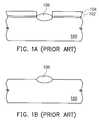
- FIGS. 1A through 1Dare schematic, cross-sectional views, illustrating successive steps of fabricating a silicon nitride floating gate for a read-only memory according to the prior art.
- a pad oxide layer 102 and a silicon nitride layer 104are sequentially formed on a provided substrate 100 .
- the silicon nitride layer 104 and the pad oxide layer 102are then patterned to expose a portion of the substrate 100 .
- thermal oxidationis conducted to form a field oxide layer 106 on the exposed substrate 100 .
- the silicon nitride layer 104 and the pad oxide layer 102are further removed, leaving the field oxide layer 106 on the substrate 100 .
- an oxide layer 108 and a silicon nitride layer 110are sequentially formed on the substrate 100 .
- a wet oxidation processis then conducted to form an oxide layer 112 .
- the oxide layer 112 , the silicon nitride layer 110 and the oxide layer 108are further patterned to form an oxide layer-nitride layer-oxide layer (ONO) structure of a tunnel oxide layer 108 a , a silicon nitride floating gate layer 110 a and an oxide dielectric layer 112 a .
- ONOoxide layer-nitride layer-oxide layer
- a polysilicon control gate structure layeris also formed on the silicon oxide dielectric layer 112 a .
- the silicon oxide dielectric layer 112 ais formed subsequent to the formation of the field oxide layer 106 . The manufacturing process is thus more time consuming, complicated and costly.
- the inventionprovides a fabrication method for a silicon oxide layer-silicon nitride layer-silicon oxide layer structure and a field oxide layer of a flash memory device, to simply the overall manufacturing process.
- the present inventionprovides a combined fabrication of a silicon oxide layer-silicon nitride layer-silicon oxide layer structure and a field oxide layer, to greatly reduce the processing steps and cost
- the inventionprovides a fabrication method for a silicon nitride read-only memory, wherein a first oxide layer and a silicon nitride layer are sequentially formed on a provided substrate.
- the first oxide layer and the silicon nitride layerare then patterned to form an opening, exposing a part of the substrate.
- an oxidation processis conducted to form a second oxide layer on the silicon nitride layer, wherein concurrently, a field oxide layer is formed on the exposed part of the substrate.
- the second oxide layer, the silicon nitride layer and the first oxide layerare then patterned to form an oxide dielectric layer, a silicon nitride floating gate layer and an oxide tunnel layer.
- a combined manufacturing of the oxide dielectric layer and the field oxide layeris provided to greatly reduce the number of manufacturing steps and simply the manufacturing process.
- a combined manufacturing of the oxide dielectric layer and the field oxide layeris provided to greatly reduce the manufacturing cost.
- FIGS. 1A through 1Dare schematic, cross-sectional views, illustrating successive steps of fabricating a silicon nitride floating gate for a read-only memory according to the prior art.
- FIGS. 2A through 2Care schematic, cross-sectional views, illustrating successive steps of fabricating a silicon nitride floating gate for a read-only memory according to a preferred embodiment of the present invention.
- FIGS. 2A through 2Care schematic, cross-sectional views, illustrating successive steps of fabricating a silicon nitride floating gate for a read-only memory according a preferred embodiment of the present invention.
- a substrate 200is provided.
- An oxide layer 208is formed on the substrate 200 , wherein the oxide layer 208 , about 50 angstroms to about 100 angstroms thick, is formed by, for example, thermal oxidation.
- a silicon nitride layer 210is then formed on the oxide layer 208 .
- the silicon nitride layer 210about 120 angstroms to about 180 angstroms thick, is formed by, for example, chemical vapor deposition. Thereafter, the silicon nitride layer 210 and the oxide layer 208 are patterned to form an opening 211 , exposing a portion of the substrate 200 .
- a thermal oxidation processis conducted to form concurrently an oxide layer 212 on the silicon nitride layer 210 and a field oxide layer 206 on the exposed substrate 200 .
- the thermal oxidation processincludes a wet oxidation process, wherein the wet oxidation process is conducted at a temperature of about 850 degrees Celsius to about 1050 degrees Celsius, an oxygen flow rate of about 5 L/min to about 30 L/min, a hydrogen flow rate of about 2 L/min to about 20 L/min and a nitrogen flow rate of about 0 L/min to about 30 L/min for about 80 to 120 minutes.
- the oxide layer 212 and the field oxide layer 206are formed at a rate ratio of about 1:35 to 1:45.
- the oxide layer 212is about 75 angstroms to 105 angstroms thick and the silicon nitride layer 210 , subsequent to the above patterning process is about 35 angstroms to about 65 angstroms thick. The fabrication of an oxide layer-nitride layer-oxide layer for a flash memory device is thus completed.
- an oxide layer of about 100 angstroms thickis formed on a silicon nitride layer, which is equivalent of growing an oxide layer of about 3500 angstroms to about 4500 angstroms thick on a substrate.
- the oxide layers with the desired thicknessare thus formed on the silicon nitride layer and the silicon substrate, respectively.
- forming an oxide layer 212 on a silicon nitride layer 210a field oxide layer 206 is concurrently formed on the substrate 200 exposed by the opening 211 .
- the manufacturing process for an oxide layer-nitride layer-oxide layer of a flash memory deviceis greatly simplified to reduce the manufacturing cost.
- the oxide layer 212 , the silicon nitride layer 210 and the oxide layer 208are patterned to form a tunnel oxide layer 208 a , a silicon nitride gate layer 210 a and an oxide dielectric layer 212 a .
- ionsare implanted between the ONO structures to form the buried bit line in the substrate 200 .
- a polysilicon type of control gate layeris formed on the silicon oxide dielectric layer 212 a to complete the fabrication of a flash memory device.
- the formation of the oxide dielectric layer and the field oxide layerare combined to greatly reduce the number of processing steps and to simplify the manufacturing procedure.
- the formation of the oxide dielectric layer and the field oxide layerare combined to greatly reduce the manufacturing cost.
Landscapes
- Non-Volatile Memory (AREA)
- Formation Of Insulating Films (AREA)
- Semiconductor Memories (AREA)
Abstract
Description
This application claims the priority benefit of Taiwan application serial no. 90112761, filed May 28, 2001.
1. Field of Invention
This invention relates to a fabrication method for a read-only memory device. More particularly, the present invention relates to a fabrication method for an oxide layer-nitride layer-oxide layer (ONO) structure and a field oxide layer of a flash memory device.
2. Description of Related Art
Flash memory device is an electrically-erasable-programmable-read-only memory device, which has the advantages of being programmable, erasable and the ability of retaining data when the power is interrupted. A flash memory device is thus commonly used in personal computer and electronic devices. A flash memory device is also a non-volatile type of memory (NVM), which has the advantages of being small in dimension, speedy in in data retrieval and storage, and low power consumption. Furthermore, the erasure of data in a flash memory device uses the “block-by-block” method; therefore, it also has the advantage of having a faster operational speed.
For a typical flash memory device, the floating gate and the control gate are formed with doped polysilicon. Electrons are injected into the floating gate and evenly distributed in the polysilicon layer of the floating gate during programming. However, if defects are present in the tunnel oxide layer underneath the polysilicon floating gate layer, current leakage is easily resulted to adversely affect the reliability of the device.
The current technical development on flash memory devices includes forming the floating gate with silicon nitride. The control gate, however, is still formed with polysilicon. When a voltage is applied to the control gate and the source region of this type of device to perform the programming function, electrons in the channel region near the vicinity of the drain region are injected into the silicon nitride floating gate. Since silicon nitride has the characteristic of being able to capture electrons, the electrons injected into the silicon nitride floating gate are not evenly distributed in the entire floating gate. Instead, the electrons are Gaussian distributed and concentrated locally in the floating gate. Because the electrons are concentrated locally in the floating gate, the sensitivity to any defect in the tunnel oxide layer is minimized. As a result, the occurrence of a current leakage is mitigated.
FIGS. 1A through 1D are schematic, cross-sectional views, illustrating successive steps of fabricating a silicon nitride floating gate for a read-only memory according to the prior art.
Referring to FIGS. 1A & 1B, apad oxide layer 102 and asilicon nitride layer 104 are sequentially formed on a providedsubstrate 100. Thesilicon nitride layer 104 and thepad oxide layer 102 are then patterned to expose a portion of thesubstrate 100. Thereafter, thermal oxidation is conducted to form afield oxide layer 106 on the exposedsubstrate 100. Thesilicon nitride layer 104 and thepad oxide layer 102 are further removed, leaving thefield oxide layer 106 on thesubstrate 100.
Referring to FIGS. 1C & 1D, anoxide layer 108 and asilicon nitride layer 110 are sequentially formed on thesubstrate 100. A wet oxidation process is then conducted to form anoxide layer 112. Theoxide layer 112, thesilicon nitride layer 110 and theoxide layer 108 are further patterned to form an oxide layer-nitride layer-oxide layer (ONO) structure of atunnel oxide layer 108a, a silicon nitride floatinggate layer 110aand an oxidedielectric layer 112a. Thereafter, ions are implanted between the ONO structures to form the buried bit line in thesubstrate 100. A polysilicon control gate structure layer is also formed on the silicon oxidedielectric layer 112a. According to the conventional approach in fabricating a silicon nitride read-only memory, the silicon oxidedielectric layer 112ais formed subsequent to the formation of thefield oxide layer 106. The manufacturing process is thus more time consuming, complicated and costly.
The invention provides a fabrication method for a silicon oxide layer-silicon nitride layer-silicon oxide layer structure and a field oxide layer of a flash memory device, to simply the overall manufacturing process.
The present invention provides a combined fabrication of a silicon oxide layer-silicon nitride layer-silicon oxide layer structure and a field oxide layer, to greatly reduce the processing steps and cost
The invention provides a fabrication method for a silicon nitride read-only memory, wherein a first oxide layer and a silicon nitride layer are sequentially formed on a provided substrate. The first oxide layer and the silicon nitride layer are then patterned to form an opening, exposing a part of the substrate. Thereafter, an oxidation process is conducted to form a second oxide layer on the silicon nitride layer, wherein concurrently, a field oxide layer is formed on the exposed part of the substrate. The second oxide layer, the silicon nitride layer and the first oxide layer are then patterned to form an oxide dielectric layer, a silicon nitride floating gate layer and an oxide tunnel layer.
According to the present invention, a combined manufacturing of the oxide dielectric layer and the field oxide layer is provided to greatly reduce the number of manufacturing steps and simply the manufacturing process.
According to the present invention, a combined manufacturing of the oxide dielectric layer and the field oxide layer is provided to greatly reduce the manufacturing cost.
It is to be understood that both the foregoing general description and the following detailed description are exemplary, and are intended to provide further explanation of the invention as claimed.
The accompanying drawings are included to provide a further understanding of the invention, and are incorporated in and constitute a part of this specification. The drawings illustrate embodiments of the invention and, together with the description, serve to explain the principles of the invention. In the drawings,
FIGS. 1A through 1D are schematic, cross-sectional views, illustrating successive steps of fabricating a silicon nitride floating gate for a read-only memory according to the prior art.
FIGS. 2A through 2C are schematic, cross-sectional views, illustrating successive steps of fabricating a silicon nitride floating gate for a read-only memory according to a preferred embodiment of the present invention.
FIGS. 2A through 2C are schematic, cross-sectional views, illustrating successive steps of fabricating a silicon nitride floating gate for a read-only memory according a preferred embodiment of the present invention.
As shown in FIG. 2A, asubstrate 200 is provided. Anoxide layer 208 is formed on thesubstrate 200, wherein theoxide layer 208, about 50 angstroms to about 100 angstroms thick, is formed by, for example, thermal oxidation. Asilicon nitride layer 210 is then formed on theoxide layer 208. Thesilicon nitride layer 210, about 120 angstroms to about 180 angstroms thick, is formed by, for example, chemical vapor deposition. Thereafter, thesilicon nitride layer 210 and theoxide layer 208 are patterned to form anopening 211, exposing a portion of thesubstrate 200.
Referring to FIG. 2B, a thermal oxidation process is conducted to form concurrently anoxide layer 212 on thesilicon nitride layer 210 and afield oxide layer 206 on the exposedsubstrate 200. The thermal oxidation process includes a wet oxidation process, wherein the wet oxidation process is conducted at a temperature of about 850 degrees Celsius to about 1050 degrees Celsius, an oxygen flow rate of about 5 L/min to about 30 L/min, a hydrogen flow rate of about 2 L/min to about 20 L/min and a nitrogen flow rate of about 0 L/min to about 30 L/min for about 80 to 120 minutes. Theoxide layer 212 and thefield oxide layer 206 are formed at a rate ratio of about 1:35 to 1:45. Theoxide layer 212 is about 75 angstroms to 105 angstroms thick and thesilicon nitride layer 210, subsequent to the above patterning process is about 35 angstroms to about 65 angstroms thick. The fabrication of an oxide layer-nitride layer-oxide layer for a flash memory device is thus completed.
Since an oxide layer of about 100 angstroms thick is formed on a silicon nitride layer, which is equivalent of growing an oxide layer of about 3500 angstroms to about 4500 angstroms thick on a substrate. Performing an oxidation process to form an oxide layer on the silicon nitride layer and on the silicon substrate, respectively at a rate ratio of about 1:35 to 1:45, the oxide layers with the desired thickness are thus formed on the silicon nitride layer and the silicon substrate, respectively. As a result, forming anoxide layer 212 on asilicon nitride layer 210, afield oxide layer 206 is concurrently formed on thesubstrate 200 exposed by theopening 211. The manufacturing process for an oxide layer-nitride layer-oxide layer of a flash memory device is greatly simplified to reduce the manufacturing cost.
Continuing to FIG. 2C, theoxide layer 212, thesilicon nitride layer 210 and theoxide layer 208 are patterned to form atunnel oxide layer 208a, a siliconnitride gate layer 210aand anoxide dielectric layer 212a. After this, ions are implanted between the ONO structures to form the buried bit line in thesubstrate 200. A polysilicon type of control gate layer is formed on the siliconoxide dielectric layer 212ato complete the fabrication of a flash memory device.
According to the present invention, the formation of the oxide dielectric layer and the field oxide layer are combined to greatly reduce the number of processing steps and to simplify the manufacturing procedure.
According to the present invention, the formation of the oxide dielectric layer and the field oxide layer are combined to greatly reduce the manufacturing cost.
It will be apparent to those skilled in the art that various modifications and variations can be made to the structure of the present invention without departing from the scope or spirit of the invention. In view of the foregoing, it is intended that the present invention cover modifications and variations of this invention provided they fall within the scope of the following claims and their equivalents.
Claims (21)
1. A method for fabricating a silicon nitride floating gate for a read-only memory, comprising:
providing a substrate;
forming a first oxide layer on the substrate;
forming a silicon nitride layer on the first oxide layer;
patterning the silicon nitride layer and the first oxide layer to form an opening, exposing a portion of the substrate;
forming concurrently a second oxide layer on the silicon nitride layer and a field oxide layer on the substrate exposed by the opening; and
patterning the second oxide layer, the silicon nitride layer and the first oxide layer to form an oxide dielectric layer, a silicon nitride floating gate layer and a tunnel oxide layer.
2. The method ofclaim 1 , wherein the second oxide layer and the field oxide layer are formed at a rate ratio of about 1:35 to about 1:45.
3. The method ofclaim 1 , wherein forming concurrently the second oxide layer on the silicon nitride layer and the field oxide layer on the substrate exposed by the opening include performing an oxidation process.
4. The method ofclaim 3 , wherein the oxidation process includes wet oxidation.
5. The method ofclaim 4 , wherein wet oxidation is conducted at an oxygen flow rate of about 5 L/min to about 30 L/min, a hydrogen flow rate of about 2 L/min to about 20 L/min and a nitrogen flow rate of about 0 L/min to about 30 L/min.
6. The method ofclaim 4 , wet oxidation is conducted at a temperature of about 850 degrees Celsius to about 1050 degrees Celsius.
7. The method ofclaim 4 , wherein wet oxidation is conducted for about 80 to 120 minutes.
8. The method ofclaim 1 , wherein the second oxide layer is about 75 angstroms to about 105 angstroms thick.
9. The method ofclaim 1 , wherein the silicon nitride layer is about 120 angstroms to about 180 angstroms thick.
10. The method ofclaim 1 , wherein the first oxide layer is about 50 angstroms to about 100 angstroms thick.
11. A method for fabricating a read-only memory, comprising:
providing a substrate;
forming a first oxide layer and a material layer on the substrate, wherein a portion of the substrate is not covered by the first oxide layer and the material layer; and
forming concurrently a second oxide layer on the material layer and a third oxide layer on the exposed substrate, wherein the second oxide layer on a top surface of the material layer and the material layer are retained as a gate dielectric.
12. The method ofclaim 11 , wherein the material layer includes silicon nitride layer.
13. The method ofclaim 11 , wherein the second oxide layer and the third oxide layer are formed at a rate ratio of about 1:35 to about 1:45.
14. The method ofclaim 11 , wherein forming concurrently a second oxide layer on the material layer and a third oxide layer on the exposed substrate includes performing an oxidation process.
15. The method ofclaim 14 , wherein performing the oxidation process includes performing a wet oxidation process.
16. The method ofclaim 15 , wherein the wet oxidation process is conducted at an oxygen flow rate of about 5 L/min to about 30 L/min, a hydrogen flow rate of about 2 L/min to about 20 L/min and a nitrogen flow rate of about 0 L/min to about 30 L/min.
17. The method ofclaim 15 , wherein the wet oxidation process is conducted at a temperature of about 850 degrees Celsius to about 1050 degree Celsius.
18. The method ofclaim 15 , wherein the wet oxidation is conducted for about 80 minutes to about 120 minutes.
19. The method ofclaim 11 , wherein the second oxide layer is about 75 angstroms to about 105 angstroms thick.
20. The method ofclaim 11 , wherein the material layer is about 120 angstroms to about 180 angstroms thick.
21. The method ofclaim 11 , wherein the first oxide layer is about 50 angstroms to about 100 angstroms thick.
Applications Claiming Priority (3)
| Application Number | Priority Date | Filing Date | Title |
|---|---|---|---|
| TW090112761ATW494541B (en) | 2001-05-28 | 2001-05-28 | Method for producing silicon nitride read-only-memory |
| TW90112761 | 2001-05-28 | ||
| TW90112761A | 2001-05-28 |
Publications (2)
| Publication Number | Publication Date |
|---|---|
| US20020177275A1 US20020177275A1 (en) | 2002-11-28 |
| US6613632B2true US6613632B2 (en) | 2003-09-02 |
Family
ID=21678355
Family Applications (1)
| Application Number | Title | Priority Date | Filing Date |
|---|---|---|---|
| US10/158,260Expired - LifetimeUS6613632B2 (en) | 2001-05-28 | 2002-05-28 | Fabrication method for a silicon nitride read-only memory |
Country Status (2)
| Country | Link |
|---|---|
| US (1) | US6613632B2 (en) |
| TW (1) | TW494541B (en) |
Cited By (23)
| Publication number | Priority date | Publication date | Assignee | Title |
|---|---|---|---|---|
| US20030235075A1 (en)* | 2002-06-21 | 2003-12-25 | Micron Technology, Inc. | Vertical NROM having a storage density of 1bit per 1F2 |
| US20040130934A1 (en)* | 2002-06-21 | 2004-07-08 | Micron Technology, Inc. | NROM memory cell, memory array, related devices and methods |
| US6830963B1 (en) | 2003-10-09 | 2004-12-14 | Micron Technology, Inc. | Fully depleted silicon-on-insulator CMOS logic |
| US20050030792A1 (en)* | 2003-08-07 | 2005-02-10 | Micron Technology, Inc. | Method for programming and erasing an nrom cell |
| US20050030794A1 (en)* | 2003-08-07 | 2005-02-10 | Micron Technology, Inc. | Method for erasing an NROM cell |
| US6878991B1 (en) | 2004-01-30 | 2005-04-12 | Micron Technology, Inc. | Vertical device 4F2 EEPROM memory |
| US20050106811A1 (en)* | 2003-11-17 | 2005-05-19 | Micron Technology, Inc. | NROM flash memory devices on ultrathin silicon |
| US20050105341A1 (en)* | 2003-11-04 | 2005-05-19 | Micron Technology, Inc. | NROM flash memory with self-aligned structural charge separation |
| US20050128804A1 (en)* | 2003-12-16 | 2005-06-16 | Micron Technology, Inc. | Multi-state NROM device |
| US20050138262A1 (en)* | 2003-12-18 | 2005-06-23 | Micron Technology, Inc. | Flash memory having a high-permittivity tunnel dielectric |
| US20050174847A1 (en)* | 2004-02-10 | 2005-08-11 | Micron Technology, Inc. | Nrom flash memory cell with integrated dram |
| US20050173755A1 (en)* | 2004-02-10 | 2005-08-11 | Micron Technology, Inc. | NROM flash memory with a high-permittivity gate dielectric |
| US20050185466A1 (en)* | 2004-02-24 | 2005-08-25 | Micron Technology, Inc. | Multi-state memory cell with asymmetric charge trapping |
| US20050212033A1 (en)* | 2004-03-24 | 2005-09-29 | Micron Technology, Inc. | Memory device with high dielectric constant gate dielectrics and metal floating gates |
| US20050247972A1 (en)* | 2004-05-06 | 2005-11-10 | Micron Technology, Inc. | Ballistic direct injection NROM cell on strained silicon structures |
| US20050253186A1 (en)* | 2003-09-05 | 2005-11-17 | Micron Technology, Inc. | Trench corner effect bidirectional flash memory cell |
| US6979857B2 (en) | 2003-07-01 | 2005-12-27 | Micron Technology, Inc. | Apparatus and method for split gate NROM memory |
| US20060124967A1 (en)* | 2003-12-16 | 2006-06-15 | Micron Technology, Inc. | NROM memory cell, memory array, related devices and methods |
| US7075146B2 (en) | 2004-02-24 | 2006-07-11 | Micron Technology, Inc. | 4F2 EEPROM NROM memory arrays with vertical devices |
| US7095075B2 (en) | 2003-07-01 | 2006-08-22 | Micron Technology, Inc. | Apparatus and method for split transistor memory having improved endurance |
| US20070117353A1 (en)* | 2003-11-25 | 2007-05-24 | Macronix International Co., Ltd. | Method for Forming Oxide on Ono Structure |
| US7232724B1 (en)* | 2005-04-25 | 2007-06-19 | Advanced Micro Devices, Inc. | Radical oxidation for bitline oxide of SONOS |
| US7241654B2 (en) | 2003-12-17 | 2007-07-10 | Micron Technology, Inc. | Vertical NROM NAND flash memory array |
Families Citing this family (3)
| Publication number | Priority date | Publication date | Assignee | Title |
|---|---|---|---|---|
| US6610586B1 (en)* | 2002-09-04 | 2003-08-26 | Macronix International Co., Ltd. | Method for fabricating nitride read-only memory |
| US20070026605A1 (en)* | 2005-08-01 | 2007-02-01 | Macronix International Co., Ltd. | Fabricating approach for memory device |
| US8729635B2 (en)* | 2006-01-18 | 2014-05-20 | Macronix International Co., Ltd. | Semiconductor device having a high stress material layer |
Citations (2)
| Publication number | Priority date | Publication date | Assignee | Title |
|---|---|---|---|---|
| US5756390A (en)* | 1996-02-27 | 1998-05-26 | Micron Technology, Inc. | Modified LOCOS process for sub-half-micron technology |
| US6187640B1 (en)* | 1998-11-17 | 2001-02-13 | Fujitsu Limited | Semiconductor device manufacturing method including various oxidation steps with different concentration of chlorine to form a field oxide |
- 2001
- 2001-05-28TWTW090112761Apatent/TW494541B/ennot_activeIP Right Cessation
- 2002
- 2002-05-28USUS10/158,260patent/US6613632B2/ennot_activeExpired - Lifetime
Patent Citations (2)
| Publication number | Priority date | Publication date | Assignee | Title |
|---|---|---|---|---|
| US5756390A (en)* | 1996-02-27 | 1998-05-26 | Micron Technology, Inc. | Modified LOCOS process for sub-half-micron technology |
| US6187640B1 (en)* | 1998-11-17 | 2001-02-13 | Fujitsu Limited | Semiconductor device manufacturing method including various oxidation steps with different concentration of chlorine to form a field oxide |
Cited By (135)
| Publication number | Priority date | Publication date | Assignee | Title |
|---|---|---|---|---|
| US7220634B2 (en) | 2002-06-21 | 2007-05-22 | Micron Technology, Inc. | NROM memory cell, memory array, related devices and methods |
| US20040066672A1 (en)* | 2002-06-21 | 2004-04-08 | Micron Technology, Inc. | Vertical NROM having a storage density of 1 bit per IF2 |
| US20040130934A1 (en)* | 2002-06-21 | 2004-07-08 | Micron Technology, Inc. | NROM memory cell, memory array, related devices and methods |
| US20040202032A1 (en)* | 2002-06-21 | 2004-10-14 | Micron Technology, Inc. | Vertical NROM having a storage density of 1 bit per 1F2 |
| US20060124998A1 (en)* | 2002-06-21 | 2006-06-15 | Micron Technology, Inc. | NROM memory cell, memory array, related devices and methods |
| US6842370B2 (en) | 2002-06-21 | 2005-01-11 | Micron Technology, Inc. | Vertical NROM having a storage density of 1 bit per 1F2 |
| US6853587B2 (en) | 2002-06-21 | 2005-02-08 | Micron Technology, Inc. | Vertical NROM having a storage density of 1 bit per 1F2 |
| US20090010075A9 (en)* | 2002-06-21 | 2009-01-08 | Micron Technologies, Inc. | NROM memory cell, memory array, related devices and methods |
| US20030235075A1 (en)* | 2002-06-21 | 2003-12-25 | Micron Technology, Inc. | Vertical NROM having a storage density of 1bit per 1F2 |
| US20060126398A1 (en)* | 2002-06-21 | 2006-06-15 | Micron Technologies, Inc. | NROM memory cell, memory array, related devices and methods |
| US8441056B2 (en) | 2002-06-21 | 2013-05-14 | Micron Technology, Inc. | NROM memory cell, memory array, related devices and methods |
| US20090072303A9 (en)* | 2002-06-21 | 2009-03-19 | Micron Technology, Inc. | Nrom memory cell, memory array, related devices and methods |
| US7230848B2 (en) | 2002-06-21 | 2007-06-12 | Micron Technology, Inc. | Vertical NROM having a storage density of 1 bit per 1F2 |
| US20050255647A1 (en)* | 2002-06-21 | 2005-11-17 | Micron Technology, Inc. | Vertical NROM having a storage density of 1 bit per 1F2 |
| US6906953B2 (en) | 2002-06-21 | 2005-06-14 | Micron Technology, Inc. | Vertical NROM having a storage density of 1 bit per 1F2 |
| US7535048B2 (en) | 2002-06-21 | 2009-05-19 | Micron Technology, Inc. | NROM memory cell, memory array, related devices and methods |
| US7541242B2 (en) | 2002-06-21 | 2009-06-02 | Micron Technology, Inc. | NROM memory cell, memory array, related devices and methods |
| US7095075B2 (en) | 2003-07-01 | 2006-08-22 | Micron Technology, Inc. | Apparatus and method for split transistor memory having improved endurance |
| US6979857B2 (en) | 2003-07-01 | 2005-12-27 | Micron Technology, Inc. | Apparatus and method for split gate NROM memory |
| US7719046B2 (en) | 2003-07-01 | 2010-05-18 | Micron Technology, Inc. | Apparatus and method for trench transistor memory having different gate dielectric thickness |
| US7227787B2 (en) | 2003-08-07 | 2007-06-05 | Micron Technology, Inc. | Method for erasing an NROM cell |
| US7075832B2 (en) | 2003-08-07 | 2006-07-11 | Micron Technology, Inc. | Method for erasing an NROM cell |
| US7639530B2 (en) | 2003-08-07 | 2009-12-29 | Micron Technology, Inc. | Method for programming and erasing an NROM cell |
| US7986555B2 (en)* | 2003-08-07 | 2011-07-26 | Micron Technology, Inc. | Method for programming and erasing an NROM cell |
| US20060133152A1 (en)* | 2003-08-07 | 2006-06-22 | Micron Technology, Inc. | Method for programming and erasing an NROM cell |
| US20070064466A1 (en)* | 2003-08-07 | 2007-03-22 | Micron Technology, Inc. | Method for programming and erasing an NROM cell |
| US20050141278A1 (en)* | 2003-08-07 | 2005-06-30 | Micron Technology, Inc. | Method for programming and erasing an NROM cell |
| US20050174855A1 (en)* | 2003-08-07 | 2005-08-11 | Micron Technology, Inc. | Method for erasing an NROM cell |
| US7075831B2 (en) | 2003-08-07 | 2006-07-11 | Micron Technology, Inc. | Method for erasing an NROM cell |
| US20100067307A1 (en)* | 2003-08-07 | 2010-03-18 | Micron Technology, Inc. | Method for programming and erasing an nrom cell |
| US7272045B2 (en) | 2003-08-07 | 2007-09-18 | Micron Technology, Inc. | Method for programming and erasing an NROM cell |
| US7085170B2 (en) | 2003-08-07 | 2006-08-01 | Micron Technology, Ind. | Method for erasing an NROM cell |
| US7277321B2 (en) | 2003-08-07 | 2007-10-02 | Micron Technology, Inc. | Method for programming and erasing an NROM cell |
| US6873550B2 (en) | 2003-08-07 | 2005-03-29 | Micron Technology, Inc. | Method for programming and erasing an NROM cell |
| US20050030794A1 (en)* | 2003-08-07 | 2005-02-10 | Micron Technology, Inc. | Method for erasing an NROM cell |
| US20050030792A1 (en)* | 2003-08-07 | 2005-02-10 | Micron Technology, Inc. | Method for programming and erasing an nrom cell |
| US7088619B2 (en) | 2003-08-07 | 2006-08-08 | Micron Technology, Inc. | Method for programming and erasing an NROM cell |
| US20050255638A1 (en)* | 2003-09-05 | 2005-11-17 | Micron Technology, Inc. | Trench corner effect bidirectional flash memory cell |
| US20050258480A1 (en)* | 2003-09-05 | 2005-11-24 | Micron Technology, Inc. | Trench corner effect bidirectional flash memory cell |
| US7283394B2 (en) | 2003-09-05 | 2007-10-16 | Micron Technology, Inc. | Trench corner effect bidirectional flash memory cell |
| US7329920B2 (en) | 2003-09-05 | 2008-02-12 | Micron Technology, Inc. | Trench corner effect bidirectional flash memory cell |
| US6977412B2 (en) | 2003-09-05 | 2005-12-20 | Micron Technology, Inc. | Trench corner effect bidirectional flash memory cell |
| US7285821B2 (en) | 2003-09-05 | 2007-10-23 | Micron Technology, Inc. | Trench corner effect bidirectional flash memory cell |
| US20050269625A1 (en)* | 2003-09-05 | 2005-12-08 | Micron Technology, Inc. | Trench corner effect bidirectional flash memory cell |
| US7161217B2 (en) | 2003-09-05 | 2007-01-09 | Micron Technology, Inc. | Trench corner effect bidirectional flash memory cell |
| US20050253186A1 (en)* | 2003-09-05 | 2005-11-17 | Micron Technology, Inc. | Trench corner effect bidirectional flash memory cell |
| US7535054B2 (en) | 2003-09-05 | 2009-05-19 | Micron Technology, Inc. | Trench corner effect bidirectional flash memory cell |
| US7973370B2 (en) | 2003-10-09 | 2011-07-05 | Micron Technology, Inc. | Fully depleted silicon-on-insulator CMOS logic |
| US6830963B1 (en) | 2003-10-09 | 2004-12-14 | Micron Technology, Inc. | Fully depleted silicon-on-insulator CMOS logic |
| US20110204431A1 (en)* | 2003-10-09 | 2011-08-25 | Micron Technology, Inc. | Fully depleted silicon-on-insulator cmos logic |
| US20050077564A1 (en)* | 2003-10-09 | 2005-04-14 | Micron Technology, Inc. | Fully depleted silicon-on-insulator CMOS logic |
| US8174081B2 (en) | 2003-10-09 | 2012-05-08 | Micron Technology, Inc. | Fully depleted silicon-on-insulator CMOS logic |
| US7078770B2 (en) | 2003-10-09 | 2006-07-18 | Micron Technology, Inc. | Fully depleted silicon-on-insulator CMOS logic |
| US7480186B2 (en) | 2003-11-04 | 2009-01-20 | Micron Technology, Inc. | NROM flash memory with self-aligned structural charge separation |
| US7184315B2 (en) | 2003-11-04 | 2007-02-27 | Micron Technology, Inc. | NROM flash memory with self-aligned structural charge separation |
| US20050105341A1 (en)* | 2003-11-04 | 2005-05-19 | Micron Technology, Inc. | NROM flash memory with self-aligned structural charge separation |
| US20070109871A1 (en)* | 2003-11-04 | 2007-05-17 | Micron Technology, Inc. | NROM flash memory with self-aligned structural charge separation |
| US20050280094A1 (en)* | 2003-11-17 | 2005-12-22 | Micron Technology, Inc. | NROM flash memory devices on ultrathin silicon |
| US7358562B2 (en) | 2003-11-17 | 2008-04-15 | Micron Technology, Inc. | NROM flash memory devices on ultrathin silicon |
| US8183625B2 (en) | 2003-11-17 | 2012-05-22 | Micron Technology, Inc. | NROM flash memory devices on ultrathin silicon |
| US20050106811A1 (en)* | 2003-11-17 | 2005-05-19 | Micron Technology, Inc. | NROM flash memory devices on ultrathin silicon |
| US7276413B2 (en) | 2003-11-17 | 2007-10-02 | Micron Technology, Inc. | NROM flash memory devices on ultrathin silicon |
| US20110163321A1 (en)* | 2003-11-17 | 2011-07-07 | Micron Technology, Inc. | Nrom flash memory devices on ultrathin silicon |
| US20080203467A1 (en)* | 2003-11-17 | 2008-08-28 | Micron Technology, Inc. | Nrom flash memory devices on ultrathin silicon |
| US7915669B2 (en) | 2003-11-17 | 2011-03-29 | Micron Technology, Inc. | NROM flash memory devices on ultrathin silicon |
| US7276762B2 (en) | 2003-11-17 | 2007-10-02 | Micron Technology, Inc. | NROM flash memory devices on ultrathin silicon |
| US7378316B2 (en) | 2003-11-17 | 2008-05-27 | Micron Technology, Inc. | Method for fabricating semiconductor vertical NROM memory cells |
| US20100270610A1 (en)* | 2003-11-17 | 2010-10-28 | Micron Technology, Inc. | Nrom flash memory devices on ultrathin silicon |
| US7202523B2 (en) | 2003-11-17 | 2007-04-10 | Micron Technology, Inc. | NROM flash memory devices on ultrathin silicon |
| US7768058B2 (en) | 2003-11-17 | 2010-08-03 | Micron Technology, Inc. | NROM flash memory devices on ultrathin silicon |
| US20070170496A1 (en)* | 2003-11-17 | 2007-07-26 | Micron Technology, Inc. | Nrom flash memory devices on ultrathin silicon |
| US20050280089A1 (en)* | 2003-11-17 | 2005-12-22 | Micron Technology, Inc. | NROM flash memory devices on ultrathin silicon |
| US7244987B2 (en) | 2003-11-17 | 2007-07-17 | Micron Technology, Inc. | NROM flash memory devices on ultrathin silicon |
| US20070166927A1 (en)* | 2003-11-17 | 2007-07-19 | Micron Technology, Inc. | Nrom flash memory devices on ultrathin silicon |
| US20070117353A1 (en)* | 2003-11-25 | 2007-05-24 | Macronix International Co., Ltd. | Method for Forming Oxide on Ono Structure |
| US7919372B2 (en)* | 2003-11-25 | 2011-04-05 | Macronix International, Co. Ltd. | Method for forming oxide on ONO structure |
| US20060124992A1 (en)* | 2003-12-16 | 2006-06-15 | Micron Technology, Inc. | NROM memory cell, memory array, related devices and methods |
| US7238599B2 (en) | 2003-12-16 | 2007-07-03 | Micron Technology, Inc. | Multi-state NROM device |
| US7050330B2 (en) | 2003-12-16 | 2006-05-23 | Micron Technology, Inc. | Multi-state NROM device |
| US20060128104A1 (en)* | 2003-12-16 | 2006-06-15 | Micron Technology, Inc. | NROM memory cell, memory array, related devices and methods |
| US7750389B2 (en) | 2003-12-16 | 2010-07-06 | Micron Technology, Inc. | NROM memory cell, memory array, related devices and methods |
| US7269071B2 (en) | 2003-12-16 | 2007-09-11 | Micron Technology, Inc. | NROM memory cell, memory array, related devices and methods |
| US7269072B2 (en) | 2003-12-16 | 2007-09-11 | Micron Technology, Inc. | NROM memory cell, memory array, related devices and methods |
| US7371642B2 (en) | 2003-12-16 | 2008-05-13 | Micron Technology, Inc. | Multi-state NROM device |
| US20060128103A1 (en)* | 2003-12-16 | 2006-06-15 | Micron Technology, Inc. | NROM memory cell, memory array, related devices and methods |
| US20060152978A1 (en)* | 2003-12-16 | 2006-07-13 | Micron Technology, Inc. | Multi-state NROM device |
| US20060124967A1 (en)* | 2003-12-16 | 2006-06-15 | Micron Technology, Inc. | NROM memory cell, memory array, related devices and methods |
| US20060166443A1 (en)* | 2003-12-16 | 2006-07-27 | Micron Technology, Inc. | Multi-state NROM device |
| US20050128804A1 (en)* | 2003-12-16 | 2005-06-16 | Micron Technology, Inc. | Multi-state NROM device |
| US7301804B2 (en) | 2003-12-16 | 2007-11-27 | Micro Technology, Inc. | NROM memory cell, memory array, related devices and methods |
| US7339239B2 (en) | 2003-12-17 | 2008-03-04 | Micron Technology, Inc. | Vertical NROM NAND flash memory array |
| US7241654B2 (en) | 2003-12-17 | 2007-07-10 | Micron Technology, Inc. | Vertical NROM NAND flash memory array |
| US7157769B2 (en) | 2003-12-18 | 2007-01-02 | Micron Technology, Inc. | Flash memory having a high-permittivity tunnel dielectric |
| US7528037B2 (en) | 2003-12-18 | 2009-05-05 | Micron Technology, Inc. | Flash memory having a high-permittivity tunnel dielectric |
| US20050277243A1 (en)* | 2003-12-18 | 2005-12-15 | Micron Technology, Inc. | Flash memory having a high-permittivity tunnel dielectric |
| US20050138262A1 (en)* | 2003-12-18 | 2005-06-23 | Micron Technology, Inc. | Flash memory having a high-permittivity tunnel dielectric |
| US20090191676A1 (en)* | 2003-12-18 | 2009-07-30 | Micron Technology, Inc. | Flash memory having a high-permittivity tunnel dielectric |
| US7332773B2 (en) | 2004-01-30 | 2008-02-19 | Micron Technology, Inc. | Vertical device 4F2 EEPROM memory |
| US7157771B2 (en) | 2004-01-30 | 2007-01-02 | Micron Technology, Inc. | Vertical device 4F2 EEPROM memory |
| US6878991B1 (en) | 2004-01-30 | 2005-04-12 | Micron Technology, Inc. | Vertical device 4F2 EEPROM memory |
| US20050174847A1 (en)* | 2004-02-10 | 2005-08-11 | Micron Technology, Inc. | Nrom flash memory cell with integrated dram |
| US7221018B2 (en) | 2004-02-10 | 2007-05-22 | Micron Technology, Inc. | NROM flash memory with a high-permittivity gate dielectric |
| US7072213B2 (en) | 2004-02-10 | 2006-07-04 | Micron Technology, Inc. | NROM flash memory cell with integrated DRAM |
| US20050275011A1 (en)* | 2004-02-10 | 2005-12-15 | Micron Technology, Inc. | NROM flash memory with a high-permittivity gate dielectric |
| US7479428B2 (en) | 2004-02-10 | 2009-01-20 | Leonard Forbes | NROM flash memory with a high-permittivity gate dielectric |
| US7319613B2 (en) | 2004-02-10 | 2008-01-15 | Micron Technology, Inc. | NROM flash memory cell with integrated DRAM |
| US20050173755A1 (en)* | 2004-02-10 | 2005-08-11 | Micron Technology, Inc. | NROM flash memory with a high-permittivity gate dielectric |
| US20050240867A1 (en)* | 2004-02-10 | 2005-10-27 | Micron Technology, Inc. | NROM flash memory cell with integrated DRAM |
| US6952366B2 (en) | 2004-02-10 | 2005-10-04 | Micron Technology, Inc. | NROM flash memory cell with integrated DRAM |
| US20060019453A1 (en)* | 2004-02-10 | 2006-01-26 | Micron Technology, Inc. | NROM flash memory with a high-permittivity gate dielectric |
| US7616482B2 (en) | 2004-02-24 | 2009-11-10 | Micron Technology, Inc. | Multi-state memory cell with asymmetric charge trapping |
| US7072217B2 (en) | 2004-02-24 | 2006-07-04 | Micron Technology, Inc. | Multi-state memory cell with asymmetric charge trapping |
| US7282762B2 (en) | 2004-02-24 | 2007-10-16 | Micron Technology, Inc. | 4F2 EEPROM NROM memory arrays with vertical devices |
| US20060203554A1 (en)* | 2004-02-24 | 2006-09-14 | Micron Technology, Inc. | Multi-state memory cell with asymmetric charge trapping |
| US20060203555A1 (en)* | 2004-02-24 | 2006-09-14 | Micron Technology, Inc. | Multi-state memory cell with asymmetric charge trapping |
| US7577027B2 (en) | 2004-02-24 | 2009-08-18 | Micron Technology, Inc. | Multi-state memory cell with asymmetric charge trapping |
| US20100039869A1 (en)* | 2004-02-24 | 2010-02-18 | Micron Technology, Inc. | Multi-state memory cell with asymmetric charge trapping |
| US20050185466A1 (en)* | 2004-02-24 | 2005-08-25 | Micron Technology, Inc. | Multi-state memory cell with asymmetric charge trapping |
| US7911837B2 (en) | 2004-02-24 | 2011-03-22 | Micron Technology, Inc. | Multi-state memory cell with asymmetric charge trapping |
| US7075146B2 (en) | 2004-02-24 | 2006-07-11 | Micron Technology, Inc. | 4F2 EEPROM NROM memory arrays with vertical devices |
| US20050280048A1 (en)* | 2004-03-24 | 2005-12-22 | Micron Technology, Inc. | Memory device with high dielectric constant gate dielectrics and metal floating gates |
| US20050212033A1 (en)* | 2004-03-24 | 2005-09-29 | Micron Technology, Inc. | Memory device with high dielectric constant gate dielectrics and metal floating gates |
| US7586144B2 (en) | 2004-03-24 | 2009-09-08 | Micron Technology, Inc. | Memory device with high dielectric constant gate dielectrics and metal floating gates |
| US7550339B2 (en) | 2004-03-24 | 2009-06-23 | Micron Technology, Inc. | Memory device with high dielectric constant gate dielectrics and metal floating gates |
| US20090294830A1 (en)* | 2004-03-24 | 2009-12-03 | Micron Technology, Inc. | Memory device with high dielectric constant gate dielectrics and metal floating gates |
| US7268031B2 (en) | 2004-03-24 | 2007-09-11 | Micron Technology, Inc. | Memory device with high dielectric constant gate dielectrics and metal floating gates |
| US8076714B2 (en) | 2004-03-24 | 2011-12-13 | Micron Technology, Inc. | Memory device with high dielectric constant gate dielectrics and metal floating gates |
| US7102191B2 (en) | 2004-03-24 | 2006-09-05 | Micron Technologies, Inc. | Memory device with high dielectric constant gate dielectrics and metal floating gates |
| US20060237775A1 (en)* | 2004-03-24 | 2006-10-26 | Micron Technology, Inc. | Memory device with high dielectric constant gate dielectrics and metal floating gates |
| US7683424B2 (en) | 2004-05-06 | 2010-03-23 | Micron Technology, Inc. | Ballistic direct injection NROM cell on strained silicon structures |
| US20060214220A1 (en)* | 2004-05-06 | 2006-09-28 | Micron Technology, Inc. | Ballistic direct injection NROM cell on strained silicon structures |
| US7274068B2 (en) | 2004-05-06 | 2007-09-25 | Micron Technology, Inc. | Ballistic direct injection NROM cell on strained silicon structures |
| US7859046B2 (en) | 2004-05-06 | 2010-12-28 | Micron Technology, Inc. | Ballistic direct injection NROM cell on strained silicon structures |
| US20050247972A1 (en)* | 2004-05-06 | 2005-11-10 | Micron Technology, Inc. | Ballistic direct injection NROM cell on strained silicon structures |
| US7232724B1 (en)* | 2005-04-25 | 2007-06-19 | Advanced Micro Devices, Inc. | Radical oxidation for bitline oxide of SONOS |
Also Published As
| Publication number | Publication date |
|---|---|
| TW494541B (en) | 2002-07-11 |
| US20020177275A1 (en) | 2002-11-28 |
Similar Documents
| Publication | Publication Date | Title |
|---|---|---|
| US6613632B2 (en) | Fabrication method for a silicon nitride read-only memory | |
| JP4885420B2 (en) | Source / drain implantation during ONO formation to improve isolation of SONOS type devices | |
| CN100530600C (en) | Method of forming a non-volatile semiconductor memory device | |
| US6358796B1 (en) | Method to fabricate a non-smiling effect structure in split-gate flash with self-aligned isolation | |
| US6117730A (en) | Integrated method by using high temperature oxide for top oxide and periphery gate oxide | |
| US6252276B1 (en) | Non-volatile semiconductor memory device including assymetrically nitrogen doped gate oxide | |
| JP2889232B1 (en) | Method of manufacturing split gate type flash memory cell | |
| US8110461B2 (en) | Flash memory device and manufacturing method of the same | |
| KR20020080330A (en) | High temperature oxide deposition for eeprom devices | |
| US6001713A (en) | Methods for forming nitrogen-rich regions in a floating gate and interpoly dielectric layer in a non-volatile semiconductor memory device | |
| US6180977B1 (en) | Self-aligned edge implanted cell to reduce leakage current and improve program speed in split-gate flash | |
| US6037224A (en) | Method for growing dual oxide thickness using nitrided oxides for oxidation suppression | |
| US6756634B2 (en) | Gated semiconductor assemblies | |
| JP2699890B2 (en) | Nonvolatile semiconductor memory device | |
| JPH07240478A (en) | Method for manufacturing non-volatile semiconductor memory device | |
| US7364969B2 (en) | Semiconductor fabrication process for integrating formation of embedded nonvolatile storage device with formation of multiple transistor device types | |
| US7118968B2 (en) | Method for manufacturing interpoly dielectric | |
| JP3173907B2 (en) | Nonvolatile memory element and method of manufacturing the same | |
| KR20100080241A (en) | Method for manufacturing flash memory device | |
| US5869370A (en) | Ultra thin tunneling oxide using buffer CVD to improve edge thinning | |
| US6362047B1 (en) | Method of manufacturing EEPROM memory points | |
| US20030119262A1 (en) | Method for manufacturing non-volatile semiconductor memory device | |
| KR100685880B1 (en) | Flash Y pyrom cell and manufacturing method thereof | |
| US6500711B1 (en) | Fabrication method for an interpoly dielectric layer | |
| CN1324690C (en) | Manufacturing method of silicon nitride read-only memory |
Legal Events
| Date | Code | Title | Description |
|---|---|---|---|
| AS | Assignment | Owner name:MACRONIX INTERNATIONAL CO., LTD., TAIWAN Free format text:ASSIGNMENT OF ASSIGNORS INTEREST;ASSIGNORS:LIU, CHIEN-HUNG;PAN, SHYI-SHUH;HUANG, SHOU-WEI;REEL/FRAME:012959/0650 Effective date:20020131 | |
| STCF | Information on status: patent grant | Free format text:PATENTED CASE | |
| FPAY | Fee payment | Year of fee payment:4 | |
| FPAY | Fee payment | Year of fee payment:8 | |
| FPAY | Fee payment | Year of fee payment:12 |