US6613243B2 - Method of making a 3-D structure using an erodable mask formed from a film having a composition that varies in its direction of thickness - Google Patents
Method of making a 3-D structure using an erodable mask formed from a film having a composition that varies in its direction of thicknessDownload PDFInfo
- Publication number
- US6613243B2 US6613243B2US09/911,834US91183401AUS6613243B2US 6613243 B2US6613243 B2US 6613243B2US 91183401 AUS91183401 AUS 91183401AUS 6613243 B2US6613243 B2US 6613243B2
- Authority
- US
- United States
- Prior art keywords
- heterogeneous film
- film
- etching
- patterned
- substrate
- Prior art date
- Legal status (The legal status is an assumption and is not a legal conclusion. Google has not performed a legal analysis and makes no representation as to the accuracy of the status listed.)
- Expired - Lifetime
Links
Images


Classifications
- G—PHYSICS
- G02—OPTICS
- G02B—OPTICAL ELEMENTS, SYSTEMS OR APPARATUS
- G02B3/00—Simple or compound lenses
- G02B3/0006—Arrays
- G02B3/0012—Arrays characterised by the manufacturing method
- G02B3/0018—Reflow, i.e. characterized by the step of melting microstructures to form curved surfaces, e.g. manufacturing of moulds and surfaces for transfer etching
- B—PERFORMING OPERATIONS; TRANSPORTING
- B81—MICROSTRUCTURAL TECHNOLOGY
- B81C—PROCESSES OR APPARATUS SPECIALLY ADAPTED FOR THE MANUFACTURE OR TREATMENT OF MICROSTRUCTURAL DEVICES OR SYSTEMS
- B81C1/00—Manufacture or treatment of devices or systems in or on a substrate
- B81C1/00388—Etch mask forming
- B81C1/00396—Mask characterised by its composition, e.g. multilayer masks
- C—CHEMISTRY; METALLURGY
- C03—GLASS; MINERAL OR SLAG WOOL
- C03C—CHEMICAL COMPOSITION OF GLASSES, GLAZES OR VITREOUS ENAMELS; SURFACE TREATMENT OF GLASS; SURFACE TREATMENT OF FIBRES OR FILAMENTS MADE FROM GLASS, MINERALS OR SLAGS; JOINING GLASS TO GLASS OR OTHER MATERIALS
- C03C15/00—Surface treatment of glass, not in the form of fibres or filaments, by etching
- G—PHYSICS
- G02—OPTICS
- G02B—OPTICAL ELEMENTS, SYSTEMS OR APPARATUS
- G02B3/00—Simple or compound lenses
- G02B3/0006—Arrays
- G02B3/0012—Arrays characterised by the manufacturing method
- G—PHYSICS
- G02—OPTICS
- G02B—OPTICAL ELEMENTS, SYSTEMS OR APPARATUS
- G02B6/00—Light guides; Structural details of arrangements comprising light guides and other optical elements, e.g. couplings
- G02B6/24—Coupling light guides
- G02B6/36—Mechanical coupling means
- G02B6/3628—Mechanical coupling means for mounting fibres to supporting carriers
- G02B6/3632—Mechanical coupling means for mounting fibres to supporting carriers characterised by the cross-sectional shape of the mechanical coupling means
- G02B6/3636—Mechanical coupling means for mounting fibres to supporting carriers characterised by the cross-sectional shape of the mechanical coupling means the mechanical coupling means being grooves
- G—PHYSICS
- G02—OPTICS
- G02B—OPTICAL ELEMENTS, SYSTEMS OR APPARATUS
- G02B6/00—Light guides; Structural details of arrangements comprising light guides and other optical elements, e.g. couplings
- G02B6/24—Coupling light guides
- G02B6/36—Mechanical coupling means
- G02B6/3628—Mechanical coupling means for mounting fibres to supporting carriers
- G02B6/3684—Mechanical coupling means for mounting fibres to supporting carriers characterised by the manufacturing process of surface profiling of the supporting carrier
- G02B6/3692—Mechanical coupling means for mounting fibres to supporting carriers characterised by the manufacturing process of surface profiling of the supporting carrier with surface micromachining involving etching, e.g. wet or dry etching steps
- G—PHYSICS
- G02—OPTICS
- G02B—OPTICAL ELEMENTS, SYSTEMS OR APPARATUS
- G02B6/00—Light guides; Structural details of arrangements comprising light guides and other optical elements, e.g. couplings
- G02B6/24—Coupling light guides
- G02B6/26—Optical coupling means
- G02B6/35—Optical coupling means having switching means
- G—PHYSICS
- G02—OPTICS
- G02B—OPTICAL ELEMENTS, SYSTEMS OR APPARATUS
- G02B6/00—Light guides; Structural details of arrangements comprising light guides and other optical elements, e.g. couplings
- G02B6/24—Coupling light guides
- G02B6/36—Mechanical coupling means
- G02B6/3628—Mechanical coupling means for mounting fibres to supporting carriers
- G02B6/3632—Mechanical coupling means for mounting fibres to supporting carriers characterised by the cross-sectional shape of the mechanical coupling means
- G02B6/3644—Mechanical coupling means for mounting fibres to supporting carriers characterised by the cross-sectional shape of the mechanical coupling means the coupling means being through-holes or wall apertures
- G—PHYSICS
- G02—OPTICS
- G02B—OPTICAL ELEMENTS, SYSTEMS OR APPARATUS
- G02B6/00—Light guides; Structural details of arrangements comprising light guides and other optical elements, e.g. couplings
- G02B6/24—Coupling light guides
- G02B6/36—Mechanical coupling means
- G02B6/3628—Mechanical coupling means for mounting fibres to supporting carriers
- G02B6/3648—Supporting carriers of a microbench type, i.e. with micromachined additional mechanical structures
- G02B6/3652—Supporting carriers of a microbench type, i.e. with micromachined additional mechanical structures the additional structures being prepositioning mounting areas, allowing only movement in one dimension, e.g. grooves, trenches or vias in the microbench surface, i.e. self aligning supporting carriers
- G—PHYSICS
- G02—OPTICS
- G02B—OPTICAL ELEMENTS, SYSTEMS OR APPARATUS
- G02B6/00—Light guides; Structural details of arrangements comprising light guides and other optical elements, e.g. couplings
- G02B6/24—Coupling light guides
- G02B6/36—Mechanical coupling means
- G02B6/38—Mechanical coupling means having fibre to fibre mating means
- G02B6/3807—Dismountable connectors, i.e. comprising plugs
- G02B6/3833—Details of mounting fibres in ferrules; Assembly methods; Manufacture
- G02B6/3854—Ferrules characterised by materials
Definitions
- the present inventionrelates to miniature optical components, such as lenslets and optical components of data communications equipment. More specifically, the present invention relates to a method of manufacturing a three-dimensional structure that may be used as an optical component. However, the present invention has applicability to various other fields requiring the manufacturing of a substrate having minute surface features characterized by intricately shaped side walls.
- optical communicationsparticularly fiber optic communications.
- the use of optical signals as a vehicle to carry channeled information at high speedsis preferred in many instances to carrying channeled information at other electromagnetic wavelengths/frequencies in media such as microwave transmission lines.
- Advantages of optical mediaare, among others, high channel (band-width), greater immunity to electromagnetic interference, and lower propagation loss.
- Gbit/secGigabits per second
- optical fiber optic communicationsis accompanied by a demand for reliable and readily manufacturable optical equipment components for holding an optical waveguide, e.g. an optical fiber(s).
- Such componentsmay include optical fiber ferrules, and optical switches for selectively coupling optical fibers or the like.
- the optical fiber ferruleis a commonly utilized component of an optical fiber connector.
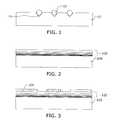
- FIG. 1schematically shows an element of a component of optical communications equipment in cross section.
- the elementwill include a holding member 10 defining one or more grooves 11 that constitute a passageway or passageways through the component.
- the passageway(s)is/are sized to accommodate a waveguide, e.g., an optical fiber(s) 12 .
- An aspect of the present inventionis to provide a method of making a three-dimensional structure having surface features of a predetermined size from a substrate.
- a more specific aspect of the present inventionis to provide a method of forming one or more grooves in a substrate that can accommodate an optical waveguide. Still further, another more specific aspect of the present invention is to provide a method of forming one or more parabolic or aspherical features in a substrate for use as lenslets.
- a heterogeneous film having a composition that varies in the direction of its thicknessis first formed on the substrate.
- the composition of the filmis selected so that the film can be etched at a rate that varies in the direction of its thickness.
- Useful examples of such thin filmsare those Silicon oxide and nitrides created by means of the technique known as Chemical Vapor Deposition, in which a precursor-bearing vapor is delivered with other reagents into a hot partial vacuum and/or plasma environment whereupon breakdown and condensation of the vapor upon the substrate results in deposition of the film.
- a continuum of graded stoichiometrycan easily be achieved in such films.
- This varying of gas ratiosmay be performed in set steps, each of pre-determined duration, or made continuous at a specified rate of change to control the “slope” of the grade in stoichiometry in the z-direction (direction of thickness) of the film.
- Adjusting the Nitrous oxide to Silane ratio in a typical oxynitride plasma-enhanced chemical vapor deposition process for example,will result in a leanness or richness of Silicon in the film.
- the filmis isotropically etched, whereby the film is patterned.
- the structure comprising the patterned heterogeneous filmis etched, during which process the film is eroded, causing increasing amounts of the substrate to become exposed to the etchant throughout the process.
- the pattern of the heterogeneous filmis in effect transferred to the substrate.
- the selectivity of the etch process(es)allows the surface features formed in the substrate to have shapes that are different from the shape embodied by the patterned heterogeneous film itself (i.e., a transfer function exists).
- relatively shallow openings in the heterogeneous filmare used to form deep pits or grooves in the substrate. These deep pits or grooves could be used as channels having the potential, because of their shape, for various uses such as for accommodating optical waveguides.
- convex bumps of a given sagare patterned in the heterogeneous film and used to form aspherical or parabolic surface features in the substrate. These surface features could be used as lenslets.
- FIG. 1(prior art) is a schematic sectional view of an element of an optical component
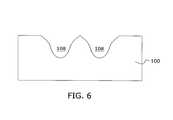
- FIGS. 2-6are each a sectional view of a substrate and collectively show the steps in a first embodiment of a method of forming a 3-D structure from the substrate according to the present invention.
- FIGS. 7-9are each a sectional view of a substrate and collectively show the steps in a second embodiment of a method of forming a 3-D structure from the substrate according to the present invention.
- a method of making a three-dimensional (3-D) structurebegins by forming a heterogeneous film 102 on a substrate 100 , e.g., a silicon substrate.
- the filmis heterogeneous in that it has a composition that varies in the direction of its thickness.
- the heterogeneous film 102is designed to etch at different rates throughout its thickness. Accordingly, the etch rates of the film 102 may vary continuously or in a step-wise manner from top to bottom.
- the heterogeneous film 102may be formed of a material whose stoichiometry varies throughout, or by sequentially forming layers of different materials on the substrate 100 .
- the layers of the heterogeneous film 102are formed/selected such that the film will etch at a rate that is faster at the upper portion thereof than at the lower portion thereof that is adjacent the substrate 100 .
- Examples of the composition of the heterogeneous film 102are as follows:
- heterogeneous film 102may comprise a combination of materials selected from the list above.
- an etch mask 104is formed on the heterogeneous film 102 .
- the etch mask 104exposes a selected portion 102 a of the heterogeneous film and may be formed by techniques that are well known, per se.
- the mask 104may be formed by a photolithographic technique in which a photoresist is deposited on the film 102 , the photoresist is exposed to light projected thereon in a certain pattern, and the exposed photoresist is then developed, whereby the photoresist is patterned.
- the mask 104may alternatively comprise a metal layer that has in turn been patterned by a photolithography and etch technique.
- the composition of the mask 104 , as well as the pattern thereof,is designed/selected based on the subsequent etch process to yield the final desired shape of the substrate as again, will become clear from the following description.
- the heterogeneous film 102is then isotropically etched using the mask 104 as an etch mask, whereby the film 102 is patterned. That is, an opening 106 is formed in the selected portion of the film 102 that was exposed by the mask 104 .
- the shape of the opening 106is dictated by the composition of the heterogeneous film 102 and the etchant. For example, in the case in which the etch rate of the heterogeneous film 102 is greatest at the upper portion of the film, the opening 106 will have the shape of a bowl or crater, i.e., the top of the opening 106 will be substantially wider than the bottom thereof.
- the mask 104will be undercut, whereby the mask 104 assumes the form of a cantilever.
- the cantilevered mask 104is characterized by an overhanging section of length “S”, namely the length by which the mask 104 is undercut and therefore projects over the opening 106 that has been etched in the film 102 .
- the mask 104is removed.
- the isotropic etching of the heterogeneous film 102is carried out using a wet etch process that produces a relatively long length “S”
- the structureshould be inverted in the bath of etchant. Consequently, overhanging portions the mask 104 will fall away from the etched heterogeneous film 102 , as shown in FIG. 5 B.
- the patterned heterogeneous film 102will serve as an erodable mask for shaping the substrate 100 . That is, the structure comprising the patterned heterogeneous film is etched to erode the film 102 and correspondingly transfer a shape into the substrate 100 . Processes that are suitable for use as this final etch process include “dry” plasma reactive ion etching (not anisotropic), anisotropic deep reactive ion etching (DRIE) and isotropic wet etching using HNA (Hydrofluoric/Nitric/Acetic acid mixture), for example.
- dry plasma reactive ion etchingnot anisotropic
- DRIEanisotropic deep reactive ion etching
- HNAHydrophilic/Nitric/Acetic acid mixture
- the selectivity of this final etch processinfluences the shape of the features formed in the substrate 100 .
- a pit 108 having a particular contour or profileis formed in the substrate 100 .
- the patterned heterogeneous filmdoes not need to be entirely removed. Rather, a thin layer of the original film 102 may remain on the substrate 100 after the final etch process.
- the final etch processhas a selectivity, or preferential rate of attack, by which the patterned heterogeneous film 102 and the substrate 100 will be etched at different rates so that the features produced in the substrate 100 do not necessarily replicate the pattern of the heterogeneous film 102 . If the final etch process etches the patterned heterogeneous film 102 at a rate that is a fraction of that at which the substrate 100 is etched, the pit 108 formed in the substrate will have a depth that is greater than that of the depth of the opening 106 in the film 102 . The higher the etch selectivity, the deeper are the features that can be produced in the substrate.
- the shapes (contour) of the pits 108will be similar to those of the openings 106 .
- the final etch process chosenhas different etch selectivities with respect to various materials constituting the heterogeneous film 102 , as will more often be the case, the patterned film 102 will erode at different rates in the direction of its thickness.
- pits 108 having shapes that are different than those of the openings 106 in the film 102will be formed in the substrate, as a function of the thickness and the etch selectivity of each individual layer in the film stack, if mask 102 is composed of discrete layers.
- the pit 108 formed in the substratewill have a depth that is the inverse multiple, in this case double, that of the depth of the corresponding opening 106 in the film 102 .
- deep contoured pitscan be formed from a heterogeneous film 102 having shallow holes.
- Deep featurese.g. pits having depths on the order of hundreds of microns, may be formed in the substrate 100 using DRIE or a wet etchant because these processes can be highly preferential to etch the Silicon of the substrate 100 over the composition of the heterogeneous film 102 .
- the shape of the features formed in the substrateare dependent on the composition of the heterogeneous film, the etchant used in the isotropic etching process shown in FIG. 3, and the etchant and etch technique used in the final etch process.
- the heterogeneous film 102is made of respective layers of SiO 2 and SiN, and has a thickness of 0.5 to 10 microns, and preferably 1 to 4 microns.
- the final etching processuses an SF 6 /O 2 plasma as an etchant, capable of providing an etch selectivity of 40:1 to 100:1 or even higher under certain known processing conditions.
- a heterogeneous film that is only three microns thickcan be used to form pits in the substrate that are three hundred microns deep. If, for example, the DRIE process is carried out under cryogenic conditions, the etch selectivity can be increased to 1000:1.
- a stoichiometrically heterogeneous film 102is formed on a substrate 100 , e.g., a Silicon substrate. Then, as shown in FIG. 7, a mask 110 of a contoured (i.e., not binary) photoresist is formed on the heterogeneous film 102 by grayscale masking or reflow techniques. Basically, as shown in the figure, a plurality of contoured mask portions are produced on the heterogeneous film 102 .
- Each of the mask portionshas a side wall that subtends an acute angle with respect to the plane of the upper surface of the heterogeneous film 102 , in contrast to the first embodiment in which the side walls of the mask extend substantially orthogonal to the plane of the upper surface of the film.
- the structure comprising the patterned grayscale mask 110is etched using a dry etch process such as RIE to transfer the pattern of the grayscale mask to the heterogeneous film 102 and thereby pattern the film 102 .
- the etching processmay be carried out until a selected portion of the substrate 102 is exposed to the etchant by the eroding resist.
- the structure comprising the patterned heterogeneous film 102is etched, whereupon the film 102 is eroded and the substrate 100 is correspondingly shaped.
- This final etching processmay also comprise RIE.
- the shape of the features formed in the substrate 102depend upon the selectivity of the (reactive ion) etch process used to transfer the pattern of the grayscale mask 110 to the heterogeneous film 102 , and the selectivity of the final etch process used to transfer the pattern of the heterogeneous film to the substrate 100 .
- the selectivities of both of the etch processes(FIGS. 7 and 8) will vary locally as a function of position (in the direction of thickness) in the heterogeneous film 102 . Therefore, a relatively simplistic pattern of the grayscale mask 110 can be used to form complex shapes in the substrate 100 . That is, the method of this embodiment does not necessarily constitute simply a proportional vertical scaling of the pattern of the grayscale mask.
- a semi-spherical portion of the patterned grayscale maskmay be used to form a parabolic feature in the substrate.
Landscapes
- Physics & Mathematics (AREA)
- Engineering & Computer Science (AREA)
- Manufacturing & Machinery (AREA)
- General Physics & Mathematics (AREA)
- Optics & Photonics (AREA)
- Chemical & Material Sciences (AREA)
- Life Sciences & Earth Sciences (AREA)
- Chemical Kinetics & Catalysis (AREA)
- General Chemical & Material Sciences (AREA)
- Geochemistry & Mineralogy (AREA)
- Materials Engineering (AREA)
- Organic Chemistry (AREA)
- Microelectronics & Electronic Packaging (AREA)
- Crystallography & Structural Chemistry (AREA)
- Drying Of Semiconductors (AREA)
Abstract
Description
Claims (15)
Priority Applications (1)
| Application Number | Priority Date | Filing Date | Title |
|---|---|---|---|
| US09/911,834US6613243B2 (en) | 2000-07-25 | 2001-07-25 | Method of making a 3-D structure using an erodable mask formed from a film having a composition that varies in its direction of thickness |
Applications Claiming Priority (2)
| Application Number | Priority Date | Filing Date | Title |
|---|---|---|---|
| US22121700P | 2000-07-25 | 2000-07-25 | |
| US09/911,834US6613243B2 (en) | 2000-07-25 | 2001-07-25 | Method of making a 3-D structure using an erodable mask formed from a film having a composition that varies in its direction of thickness |
Publications (2)
| Publication Number | Publication Date |
|---|---|
| US20020084251A1 US20020084251A1 (en) | 2002-07-04 |
| US6613243B2true US6613243B2 (en) | 2003-09-02 |
Family
ID=26915596
Family Applications (1)
| Application Number | Title | Priority Date | Filing Date |
|---|---|---|---|
| US09/911,834Expired - LifetimeUS6613243B2 (en) | 2000-07-25 | 2001-07-25 | Method of making a 3-D structure using an erodable mask formed from a film having a composition that varies in its direction of thickness |
Country Status (1)
| Country | Link |
|---|---|
| US (1) | US6613243B2 (en) |
Cited By (4)
| Publication number | Priority date | Publication date | Assignee | Title |
|---|---|---|---|---|
| US20060134922A1 (en)* | 2004-12-22 | 2006-06-22 | Taussig Carl P | Method of forming at least one thin film device |
| US20080225404A1 (en)* | 2004-03-09 | 2008-09-18 | Tang Yin S | Motionless lens systems and methods |
| US20110194179A1 (en)* | 2010-02-09 | 2011-08-11 | Roger Wen-Yi Hsu | Method and Appartus for Making Retarder in Stereoscopic Glasses |
| US8379159B2 (en) | 2010-03-12 | 2013-02-19 | Roger Wen-Yi Hsu | Method and apparatus for improved retarder of 3D glasses |
Families Citing this family (4)
| Publication number | Priority date | Publication date | Assignee | Title |
|---|---|---|---|---|
| TW200302355A (en)* | 2002-01-18 | 2003-08-01 | Nippon Sheet Glass Co Ltd | Method for producing aspherical structure, and aspherical lens array molding tool and aspherical lens array produced by the same method |
| US7572385B2 (en)* | 2003-11-17 | 2009-08-11 | Micron Technology, Inc. | Method of forming micro-lenses |
| US11205695B2 (en)* | 2017-12-21 | 2021-12-21 | Texas Instruments Incorporated | Method of fabricating a thick oxide feature on a semiconductor wafer |
| CN115498085B (en)* | 2022-10-12 | 2025-09-16 | 广东中图半导体科技股份有限公司 | Patterned composite substrate for ultraviolet LED, preparation method and epitaxial wafer |
Citations (10)
| Publication number | Priority date | Publication date | Assignee | Title |
|---|---|---|---|---|
| US4092210A (en) | 1975-08-18 | 1978-05-30 | Siemens Aktiengesellschaft | Process for the production of etched structures in a surface of a solid body by ionic etching |
| US4461672A (en) | 1982-11-18 | 1984-07-24 | Texas Instruments, Inc. | Process for etching tapered vias in silicon dioxide |
| US4908333A (en) | 1987-03-24 | 1990-03-13 | Oki Electric Industry Co., Ltd. | Process for manufacturing a semiconductor device having a contact window defined by an inclined surface of a composite film |
| US4938841A (en) | 1989-10-31 | 1990-07-03 | Bell Communications Research, Inc. | Two-level lithographic mask for producing tapered depth |
| US5275695A (en) | 1992-12-18 | 1994-01-04 | International Business Machines Corporation | Process for generating beveled edges |
| US5310623A (en) | 1992-11-27 | 1994-05-10 | Lockheed Missiles & Space Company, Inc. | Method for fabricating microlenses |
| US5528082A (en)* | 1994-04-28 | 1996-06-18 | Xerox Corporation | Thin-film structure with tapered feature |
| US5528080A (en)* | 1993-03-05 | 1996-06-18 | Goldstein; Edward F. | Electrically conductive interconnection through a body of semiconductor material |
| US6303447B1 (en)* | 2000-02-11 | 2001-10-16 | Chartered Semiconductor Manufacturing Ltd. | Method for forming an extended metal gate using a damascene process |
| US6396078B1 (en)* | 1995-06-20 | 2002-05-28 | Semiconductor Energy Laboratory Co., Ltd. | Semiconductor device with a tapered hole formed using multiple layers with different etching rates |
- 2001
- 2001-07-25USUS09/911,834patent/US6613243B2/ennot_activeExpired - Lifetime
Patent Citations (11)
| Publication number | Priority date | Publication date | Assignee | Title |
|---|---|---|---|---|
| US4092210A (en) | 1975-08-18 | 1978-05-30 | Siemens Aktiengesellschaft | Process for the production of etched structures in a surface of a solid body by ionic etching |
| US4461672A (en) | 1982-11-18 | 1984-07-24 | Texas Instruments, Inc. | Process for etching tapered vias in silicon dioxide |
| US4908333A (en) | 1987-03-24 | 1990-03-13 | Oki Electric Industry Co., Ltd. | Process for manufacturing a semiconductor device having a contact window defined by an inclined surface of a composite film |
| US4938841A (en) | 1989-10-31 | 1990-07-03 | Bell Communications Research, Inc. | Two-level lithographic mask for producing tapered depth |
| US5310623A (en) | 1992-11-27 | 1994-05-10 | Lockheed Missiles & Space Company, Inc. | Method for fabricating microlenses |
| US5480764A (en) | 1992-11-27 | 1996-01-02 | Lockheed Missiles And Space Comapny, Inc. | Gray scale microfabrication for integrated optical devices |
| US5275695A (en) | 1992-12-18 | 1994-01-04 | International Business Machines Corporation | Process for generating beveled edges |
| US5528080A (en)* | 1993-03-05 | 1996-06-18 | Goldstein; Edward F. | Electrically conductive interconnection through a body of semiconductor material |
| US5528082A (en)* | 1994-04-28 | 1996-06-18 | Xerox Corporation | Thin-film structure with tapered feature |
| US6396078B1 (en)* | 1995-06-20 | 2002-05-28 | Semiconductor Energy Laboratory Co., Ltd. | Semiconductor device with a tapered hole formed using multiple layers with different etching rates |
| US6303447B1 (en)* | 2000-02-11 | 2001-10-16 | Chartered Semiconductor Manufacturing Ltd. | Method for forming an extended metal gate using a damascene process |
Cited By (7)
| Publication number | Priority date | Publication date | Assignee | Title |
|---|---|---|---|---|
| US20080225404A1 (en)* | 2004-03-09 | 2008-09-18 | Tang Yin S | Motionless lens systems and methods |
| US7706071B2 (en)* | 2004-03-09 | 2010-04-27 | Tang Yin S | Lens systems and methods |
| US20060134922A1 (en)* | 2004-12-22 | 2006-06-22 | Taussig Carl P | Method of forming at least one thin film device |
| US7202179B2 (en)* | 2004-12-22 | 2007-04-10 | Hewlett-Packard Development Company, L.P. | Method of forming at least one thin film device |
| US20110194179A1 (en)* | 2010-02-09 | 2011-08-11 | Roger Wen-Yi Hsu | Method and Appartus for Making Retarder in Stereoscopic Glasses |
| US9005493B2 (en) | 2010-02-09 | 2015-04-14 | Roger Wen-Yi Hsu | Method and apparatus for making retarder in stereoscopic glasses |
| US8379159B2 (en) | 2010-03-12 | 2013-02-19 | Roger Wen-Yi Hsu | Method and apparatus for improved retarder of 3D glasses |
Also Published As
| Publication number | Publication date |
|---|---|
| US20020084251A1 (en) | 2002-07-04 |
Similar Documents
| Publication | Publication Date | Title |
|---|---|---|
| US5770465A (en) | Trench-filling etch-masking microfabrication technique | |
| US5738757A (en) | Planar masking for multi-depth silicon etching | |
| US7016587B2 (en) | Low loss silicon waveguide and method of fabrication thereof | |
| US5426070A (en) | Microstructures and high temperature isolation process for fabrication thereof | |
| US5719073A (en) | Microstructures and single mask, single-crystal process for fabrication thereof | |
| US7504757B2 (en) | Multi-finger z-actuator | |
| US20060121635A1 (en) | Lids for wafer-scale optoelectronic packages | |
| US6613243B2 (en) | Method of making a 3-D structure using an erodable mask formed from a film having a composition that varies in its direction of thickness | |
| US6921490B1 (en) | Optical component having waveguides extending from a common region | |
| US20030052082A1 (en) | Method of forming optical waveguides in a semiconductor substrate | |
| US6124080A (en) | Method of manufacturing an optical device with a groove accurately formed | |
| JP2008505355A (en) | Method for manufacturing an optical waveguide assembly having an integral alignment mechanism | |
| EP0599394B1 (en) | Method of manufacturing sharp waveguide branches in integrated optical components | |
| US6756319B2 (en) | Silica microstructure and fabrication method thereof | |
| WO2006136194A1 (en) | Method for fabricating a turning mirror for optical devices | |
| US20020134749A1 (en) | Method of making a vertical, mirror quality surface in silicon and mirror made by the method | |
| US6510275B1 (en) | Micro-optoelectromechanical system based device with aligned structures and method for fabricating same | |
| JP2005535137A (en) | Method for making at least one small opening in a layer on a substrate and component parts produced by such a method | |
| CA2349031A1 (en) | Method of fabricating mode-size converter with three dimensional tapered with high processing tolerance | |
| US20050211664A1 (en) | Method of forming optical waveguides in a semiconductor substrate | |
| JP4235179B2 (en) | Optical waveguide device manufacturing method and optical waveguide device | |
| KR20030071899A (en) | Method for manufacturing waveguide groove by using the dry etching | |
| US20020158047A1 (en) | Formation of an optical component having smooth sidewalls | |
| TW200527017A (en) | Constructing well structures for hybrid optical waveguides | |
| US7354522B2 (en) | Substrate etching method for forming connected features |
Legal Events
| Date | Code | Title | Description |
|---|---|---|---|
| AS | Assignment | Owner name:HALEOS, INC., VIRGINIA Free format text:ASSIGNMENT OF ASSIGNORS INTEREST;ASSIGNOR:RICKS, NEAL;REEL/FRAME:012425/0928 Effective date:20010918 | |
| AS | Assignment | Owner name:HALEOS, INC., VIRGINIA Free format text:ASSIGNMENT OF ASSIGNORS INTEREST;ASSIGNORS:STEINBERG, DAN A.;HUGHES, WILLIAM T.;DAUTARTAS, MINDAUGAS F.;AND OTHERS;REEL/FRAME:013174/0328;SIGNING DATES FROM 20020910 TO 20020920 Owner name:SHIPLEY COMPANY, L.L.C., MASSACHUSETTS Free format text:ASSIGNMENT OF ASSIGNORS INTEREST;ASSIGNOR:HALEOS, INC.;REEL/FRAME:013181/0159 Effective date:20020911 Owner name:HALEOS, INC., VIRGINIA Free format text:ASSIGNMENT OF ASSIGNORS INTEREST;ASSIGNORS:STEINBERG, DAN A.;HUGHES, WILLIAM T.;DAUTARTAS, MINDAUGAS F.;AND OTHERS;SIGNING DATES FROM 20020910 TO 20020920;REEL/FRAME:013174/0328 | |
| STCF | Information on status: patent grant | Free format text:PATENTED CASE | |
| FPAY | Fee payment | Year of fee payment:4 | |
| AS | Assignment | Owner name:NUVOTRONICS, LLC,VIRGINIA Free format text:ASSIGNMENT OF ASSIGNORS INTEREST;ASSIGNOR:ROHM AND HAAS ELECTRONIC MATERIALS LLC;REEL/FRAME:024571/0939 Effective date:20080708 Owner name:NUVOTRONICS, LLC, VIRGINIA Free format text:ASSIGNMENT OF ASSIGNORS INTEREST;ASSIGNOR:ROHM AND HAAS ELECTRONIC MATERIALS LLC;REEL/FRAME:024571/0939 Effective date:20080708 | |
| FEPP | Fee payment procedure | Free format text:PAYOR NUMBER ASSIGNED (ORIGINAL EVENT CODE: ASPN); ENTITY STATUS OF PATENT OWNER: LARGE ENTITY | |
| FPAY | Fee payment | Year of fee payment:8 | |
| AS | Assignment | Owner name:IP CUBE PARTNERS CO. LTD., KOREA, REPUBLIC OF Free format text:ASSIGNMENT OF ASSIGNORS INTEREST;ASSIGNOR:NUVOTRONICS, LLC;REEL/FRAME:025949/0867 Effective date:20100831 | |
| AS | Assignment | Owner name:SAMSUNG ELECTRONICS CO., LTD., KOREA, REPUBLIC OF Free format text:ASSIGNMENT OF ASSIGNORS INTEREST;ASSIGNOR:IP CUBE PARTNERS CO. LTD.;REEL/FRAME:026323/0651 Effective date:20110512 | |
| FPAY | Fee payment | Year of fee payment:12 | |
| AS | Assignment | Owner name:SHIPLEY COMPANY, L.L.C., MASSACHUSETTS Free format text:CORRECTIVE ASSIGNMENT TO CORRECT THE INCORRECT SERIAL NUMBER 10/013793 NEEDS TO BE REMOVED PREVIOUSLY RECORDED ON REEL 013181 FRAME 0159. ASSIGNOR(S) HEREBY CONFIRMS THE 09824205, 09824638, 09825990, 09827183, 09828842, 09833282, ET AL.;ASSIGNOR:HALEOS, INC.;REEL/FRAME:035224/0157 Effective date:20020911 Owner name:HALEOS, INC., VIRGINIA Free format text:CORRECTIVE ASSIGNMENT TO CORRECT THE INCORRECT SERIAL NO. 10/013,793 PREVIOUSLY RECORDED AT REEL: 013174 FRAME: 0328. ASSIGNOR(S) HEREBY CONFIRMS THE ASSIGNMENT;ASSIGNORS:STEINBERG, DAN A.;HUGHES, WILLIAM T.;DAUTARTAS, MINDAUGAS F.;AND OTHERS;SIGNING DATES FROM 20020910 TO 20020920;REEL/FRAME:035225/0156 |