US6612027B2 - Method for forming metal contacts on a substrate - Google Patents
Method for forming metal contacts on a substrateDownload PDFInfo
- Publication number
- US6612027B2 US6612027B2US09/942,246US94224601AUS6612027B2US 6612027 B2US6612027 B2US 6612027B2US 94224601 AUS94224601 AUS 94224601AUS 6612027 B2US6612027 B2US 6612027B2
- Authority
- US
- United States
- Prior art keywords
- substrate
- solder
- mold
- cavity
- forming
- Prior art date
- Legal status (The legal status is an assumption and is not a legal conclusion. Google has not performed a legal analysis and makes no representation as to the accuracy of the status listed.)
- Expired - Lifetime, expires
Links
- 239000000758substrateSubstances0.000titleclaimsabstractdescription185
- 229910052751metalInorganic materials0.000titleclaimsabstractdescription47
- 239000002184metalSubstances0.000titleclaimsabstractdescription47
- 238000000034methodMethods0.000titleclaimsdescription44
- 229910000679solderInorganic materials0.000claimsabstractdescription176
- 238000010438heat treatmentMethods0.000claimsdescription37
- 239000004020conductorSubstances0.000claimsdescription10
- VYPSYNLAJGMNEJ-UHFFFAOYSA-NSilicium dioxideChemical groupO=[Si]=OVYPSYNLAJGMNEJ-UHFFFAOYSA-N0.000claimsdescription5
- 238000003892spreadingMethods0.000claimsdescription3
- 229910052581Si3N4Inorganic materials0.000claimsdescription2
- HQVNEWCFYHHQES-UHFFFAOYSA-Nsilicon nitrideChemical groupN12[Si]34N5[Si]62N3[Si]51N64HQVNEWCFYHHQES-UHFFFAOYSA-N0.000claimsdescription2
- 239000011241protective layerSubstances0.000claims15
- 239000010410layerSubstances0.000claims2
- 230000000873masking effectEffects0.000claims2
- 239000007769metal materialSubstances0.000claims1
- 229910052814silicon oxideInorganic materials0.000claims1
- 239000004065semiconductorSubstances0.000abstractdescription45
- 239000000463materialSubstances0.000abstractdescription28
- 230000015572biosynthetic processEffects0.000description10
- 230000001681protective effectEffects0.000description10
- XUIMIQQOPSSXEZ-UHFFFAOYSA-NSiliconChemical compound[Si]XUIMIQQOPSSXEZ-UHFFFAOYSA-N0.000description7
- 229910052710siliconInorganic materials0.000description7
- 239000010703siliconSubstances0.000description7
- 238000010276constructionMethods0.000description4
- 238000012546transferMethods0.000description4
- 238000013459approachMethods0.000description3
- 239000011248coating agentSubstances0.000description3
- 238000000576coating methodMethods0.000description3
- 238000005530etchingMethods0.000description3
- LQBJWKCYZGMFEV-UHFFFAOYSA-Nlead tinChemical compound[Sn].[Pb]LQBJWKCYZGMFEV-UHFFFAOYSA-N0.000description3
- 238000012545processingMethods0.000description3
- NBIIXXVUZAFLBC-UHFFFAOYSA-NPhosphoric acidChemical compoundOP(O)(O)=ONBIIXXVUZAFLBC-UHFFFAOYSA-N0.000description2
- 230000005496eutecticsEffects0.000description2
- 230000005055memory storageEffects0.000description2
- 238000005459micromachiningMethods0.000description2
- 229920000642polymerPolymers0.000description2
- 235000012239silicon dioxideNutrition0.000description2
- 239000000377silicon dioxideSubstances0.000description2
- JBRZTFJDHDCESZ-UHFFFAOYSA-NAsGaChemical compound[As]#[Ga]JBRZTFJDHDCESZ-UHFFFAOYSA-N0.000description1
- RYGMFSIKBFXOCR-UHFFFAOYSA-NCopperChemical compound[Cu]RYGMFSIKBFXOCR-UHFFFAOYSA-N0.000description1
- 229910001218Gallium arsenideInorganic materials0.000description1
- ATJFFYVFTNAWJD-UHFFFAOYSA-NTinChemical compound[Sn]ATJFFYVFTNAWJD-UHFFFAOYSA-N0.000description1
- 229910000147aluminium phosphateInorganic materials0.000description1
- 230000009286beneficial effectEffects0.000description1
- 230000001413cellular effectEffects0.000description1
- 239000000919ceramicSubstances0.000description1
- 238000005229chemical vapour depositionMethods0.000description1
- 238000004140cleaningMethods0.000description1
- 229910052802copperInorganic materials0.000description1
- 239000010949copperSubstances0.000description1
- 230000002950deficientEffects0.000description1
- 238000013461designMethods0.000description1
- 238000010586diagramMethods0.000description1
- 238000005516engineering processMethods0.000description1
- 239000011521glassSubstances0.000description1
- PCHJSUWPFVWCPO-UHFFFAOYSA-NgoldChemical compound[Au]PCHJSUWPFVWCPO-UHFFFAOYSA-N0.000description1
- 229910052737goldInorganic materials0.000description1
- 239000010931goldSubstances0.000description1
- 238000011065in-situ storageMethods0.000description1
- 229910052738indiumInorganic materials0.000description1
- DGAHKUBUPHJKDE-UHFFFAOYSA-Nindium leadChemical compound[In].[Pb]DGAHKUBUPHJKDE-UHFFFAOYSA-N0.000description1
- RHZWSUVWRRXEJF-UHFFFAOYSA-Nindium tinChemical compound[In].[Sn]RHZWSUVWRRXEJF-UHFFFAOYSA-N0.000description1
- 238000009413insulationMethods0.000description1
- 239000012212insulatorSubstances0.000description1
- LWUVWAREOOAHDW-UHFFFAOYSA-Nlead silverChemical compound[Ag].[Pb]LWUVWAREOOAHDW-UHFFFAOYSA-N0.000description1
- 230000008018meltingEffects0.000description1
- 238000002844meltingMethods0.000description1
- 238000010310metallurgical processMethods0.000description1
- 150000004767nitridesChemical class0.000description1
- 238000000059patterningMethods0.000description1
- 230000035515penetrationEffects0.000description1
- 229920002120photoresistant polymerPolymers0.000description1
- 238000003825pressingMethods0.000description1
- 229910052594sapphireInorganic materials0.000description1
- 239000010980sapphireSubstances0.000description1
- 229910052709silverInorganic materials0.000description1
- 239000004332silverSubstances0.000description1
- 239000000126substanceSubstances0.000description1
- 238000009736wettingMethods0.000description1
- 210000000707wristAnatomy0.000description1
Images


Classifications
- H—ELECTRICITY
- H01—ELECTRIC ELEMENTS
- H01L—SEMICONDUCTOR DEVICES NOT COVERED BY CLASS H10
- H01L21/00—Processes or apparatus adapted for the manufacture or treatment of semiconductor or solid state devices or of parts thereof
- H01L21/67—Apparatus specially adapted for handling semiconductor or electric solid state devices during manufacture or treatment thereof; Apparatus specially adapted for handling wafers during manufacture or treatment of semiconductor or electric solid state devices or components ; Apparatus not specifically provided for elsewhere
- H01L21/683—Apparatus specially adapted for handling semiconductor or electric solid state devices during manufacture or treatment thereof; Apparatus specially adapted for handling wafers during manufacture or treatment of semiconductor or electric solid state devices or components ; Apparatus not specifically provided for elsewhere for supporting or gripping
- H01L21/6835—Apparatus specially adapted for handling semiconductor or electric solid state devices during manufacture or treatment thereof; Apparatus specially adapted for handling wafers during manufacture or treatment of semiconductor or electric solid state devices or components ; Apparatus not specifically provided for elsewhere for supporting or gripping using temporarily an auxiliary support
- H—ELECTRICITY
- H01—ELECTRIC ELEMENTS
- H01L—SEMICONDUCTOR DEVICES NOT COVERED BY CLASS H10
- H01L24/00—Arrangements for connecting or disconnecting semiconductor or solid-state bodies; Methods or apparatus related thereto
- H01L24/01—Means for bonding being attached to, or being formed on, the surface to be connected, e.g. chip-to-package, die-attach, "first-level" interconnects; Manufacturing methods related thereto
- H01L24/10—Bump connectors ; Manufacturing methods related thereto
- H01L24/11—Manufacturing methods
- H—ELECTRICITY
- H05—ELECTRIC TECHNIQUES NOT OTHERWISE PROVIDED FOR
- H05K—PRINTED CIRCUITS; CASINGS OR CONSTRUCTIONAL DETAILS OF ELECTRIC APPARATUS; MANUFACTURE OF ASSEMBLAGES OF ELECTRICAL COMPONENTS
- H05K3/00—Apparatus or processes for manufacturing printed circuits
- H05K3/30—Assembling printed circuits with electric components, e.g. with resistor
- H05K3/32—Assembling printed circuits with electric components, e.g. with resistor electrically connecting electric components or wires to printed circuits
- H05K3/34—Assembling printed circuits with electric components, e.g. with resistor electrically connecting electric components or wires to printed circuits by soldering
- H05K3/3457—Solder materials or compositions; Methods of application thereof
- H05K3/3485—Applying solder paste, slurry or powder
- H—ELECTRICITY
- H01—ELECTRIC ELEMENTS
- H01L—SEMICONDUCTOR DEVICES NOT COVERED BY CLASS H10
- H01L2224/00—Indexing scheme for arrangements for connecting or disconnecting semiconductor or solid-state bodies and methods related thereto as covered by H01L24/00
- H01L2224/01—Means for bonding being attached to, or being formed on, the surface to be connected, e.g. chip-to-package, die-attach, "first-level" interconnects; Manufacturing methods related thereto
- H01L2224/10—Bump connectors; Manufacturing methods related thereto
- H01L2224/11—Manufacturing methods
- H01L2224/11001—Involving a temporary auxiliary member not forming part of the manufacturing apparatus, e.g. removable or sacrificial coating, film or substrate
- H01L2224/11003—Involving a temporary auxiliary member not forming part of the manufacturing apparatus, e.g. removable or sacrificial coating, film or substrate for holding or transferring the bump preform
- H—ELECTRICITY
- H01—ELECTRIC ELEMENTS
- H01L—SEMICONDUCTOR DEVICES NOT COVERED BY CLASS H10
- H01L2224/00—Indexing scheme for arrangements for connecting or disconnecting semiconductor or solid-state bodies and methods related thereto as covered by H01L24/00
- H01L2224/01—Means for bonding being attached to, or being formed on, the surface to be connected, e.g. chip-to-package, die-attach, "first-level" interconnects; Manufacturing methods related thereto
- H01L2224/10—Bump connectors; Manufacturing methods related thereto
- H01L2224/11—Manufacturing methods
- H01L2224/113—Manufacturing methods by local deposition of the material of the bump connector
- H01L2224/1133—Manufacturing methods by local deposition of the material of the bump connector in solid form
- H01L2224/11334—Manufacturing methods by local deposition of the material of the bump connector in solid form using preformed bumps
- H—ELECTRICITY
- H01—ELECTRIC ELEMENTS
- H01L—SEMICONDUCTOR DEVICES NOT COVERED BY CLASS H10
- H01L2224/00—Indexing scheme for arrangements for connecting or disconnecting semiconductor or solid-state bodies and methods related thereto as covered by H01L24/00
- H01L2224/01—Means for bonding being attached to, or being formed on, the surface to be connected, e.g. chip-to-package, die-attach, "first-level" interconnects; Manufacturing methods related thereto
- H01L2224/10—Bump connectors; Manufacturing methods related thereto
- H01L2224/12—Structure, shape, material or disposition of the bump connectors prior to the connecting process
- H01L2224/13—Structure, shape, material or disposition of the bump connectors prior to the connecting process of an individual bump connector
- H01L2224/13001—Core members of the bump connector
- H01L2224/13099—Material
- H—ELECTRICITY
- H01—ELECTRIC ELEMENTS
- H01L—SEMICONDUCTOR DEVICES NOT COVERED BY CLASS H10
- H01L2224/00—Indexing scheme for arrangements for connecting or disconnecting semiconductor or solid-state bodies and methods related thereto as covered by H01L24/00
- H01L2224/01—Means for bonding being attached to, or being formed on, the surface to be connected, e.g. chip-to-package, die-attach, "first-level" interconnects; Manufacturing methods related thereto
- H01L2224/10—Bump connectors; Manufacturing methods related thereto
- H01L2224/15—Structure, shape, material or disposition of the bump connectors after the connecting process
- H01L2224/16—Structure, shape, material or disposition of the bump connectors after the connecting process of an individual bump connector
- H—ELECTRICITY
- H01—ELECTRIC ELEMENTS
- H01L—SEMICONDUCTOR DEVICES NOT COVERED BY CLASS H10
- H01L2924/00—Indexing scheme for arrangements or methods for connecting or disconnecting semiconductor or solid-state bodies as covered by H01L24/00
- H01L2924/0001—Technical content checked by a classifier
- H01L2924/00013—Fully indexed content
- H—ELECTRICITY
- H01—ELECTRIC ELEMENTS
- H01L—SEMICONDUCTOR DEVICES NOT COVERED BY CLASS H10
- H01L2924/00—Indexing scheme for arrangements or methods for connecting or disconnecting semiconductor or solid-state bodies as covered by H01L24/00
- H01L2924/01—Chemical elements
- H01L2924/01005—Boron [B]
- H—ELECTRICITY
- H01—ELECTRIC ELEMENTS
- H01L—SEMICONDUCTOR DEVICES NOT COVERED BY CLASS H10
- H01L2924/00—Indexing scheme for arrangements or methods for connecting or disconnecting semiconductor or solid-state bodies as covered by H01L24/00
- H01L2924/01—Chemical elements
- H01L2924/01006—Carbon [C]
- H—ELECTRICITY
- H01—ELECTRIC ELEMENTS
- H01L—SEMICONDUCTOR DEVICES NOT COVERED BY CLASS H10
- H01L2924/00—Indexing scheme for arrangements or methods for connecting or disconnecting semiconductor or solid-state bodies as covered by H01L24/00
- H01L2924/01—Chemical elements
- H01L2924/01015—Phosphorus [P]
- H—ELECTRICITY
- H01—ELECTRIC ELEMENTS
- H01L—SEMICONDUCTOR DEVICES NOT COVERED BY CLASS H10
- H01L2924/00—Indexing scheme for arrangements or methods for connecting or disconnecting semiconductor or solid-state bodies as covered by H01L24/00
- H01L2924/01—Chemical elements
- H01L2924/01029—Copper [Cu]
- H—ELECTRICITY
- H01—ELECTRIC ELEMENTS
- H01L—SEMICONDUCTOR DEVICES NOT COVERED BY CLASS H10
- H01L2924/00—Indexing scheme for arrangements or methods for connecting or disconnecting semiconductor or solid-state bodies as covered by H01L24/00
- H01L2924/01—Chemical elements
- H01L2924/01033—Arsenic [As]
- H—ELECTRICITY
- H01—ELECTRIC ELEMENTS
- H01L—SEMICONDUCTOR DEVICES NOT COVERED BY CLASS H10
- H01L2924/00—Indexing scheme for arrangements or methods for connecting or disconnecting semiconductor or solid-state bodies as covered by H01L24/00
- H01L2924/01—Chemical elements
- H01L2924/01047—Silver [Ag]
- H—ELECTRICITY
- H01—ELECTRIC ELEMENTS
- H01L—SEMICONDUCTOR DEVICES NOT COVERED BY CLASS H10
- H01L2924/00—Indexing scheme for arrangements or methods for connecting or disconnecting semiconductor or solid-state bodies as covered by H01L24/00
- H01L2924/01—Chemical elements
- H01L2924/01049—Indium [In]
- H—ELECTRICITY
- H01—ELECTRIC ELEMENTS
- H01L—SEMICONDUCTOR DEVICES NOT COVERED BY CLASS H10
- H01L2924/00—Indexing scheme for arrangements or methods for connecting or disconnecting semiconductor or solid-state bodies as covered by H01L24/00
- H01L2924/01—Chemical elements
- H01L2924/01057—Lanthanum [La]
- H—ELECTRICITY
- H01—ELECTRIC ELEMENTS
- H01L—SEMICONDUCTOR DEVICES NOT COVERED BY CLASS H10
- H01L2924/00—Indexing scheme for arrangements or methods for connecting or disconnecting semiconductor or solid-state bodies as covered by H01L24/00
- H01L2924/01—Chemical elements
- H01L2924/01079—Gold [Au]
- H—ELECTRICITY
- H01—ELECTRIC ELEMENTS
- H01L—SEMICONDUCTOR DEVICES NOT COVERED BY CLASS H10
- H01L2924/00—Indexing scheme for arrangements or methods for connecting or disconnecting semiconductor or solid-state bodies as covered by H01L24/00
- H01L2924/01—Chemical elements
- H01L2924/01082—Lead [Pb]
- H—ELECTRICITY
- H01—ELECTRIC ELEMENTS
- H01L—SEMICONDUCTOR DEVICES NOT COVERED BY CLASS H10
- H01L2924/00—Indexing scheme for arrangements or methods for connecting or disconnecting semiconductor or solid-state bodies as covered by H01L24/00
- H01L2924/013—Alloys
- H01L2924/0132—Binary Alloys
- H01L2924/01322—Eutectic Alloys, i.e. obtained by a liquid transforming into two solid phases
- H—ELECTRICITY
- H01—ELECTRIC ELEMENTS
- H01L—SEMICONDUCTOR DEVICES NOT COVERED BY CLASS H10
- H01L2924/00—Indexing scheme for arrangements or methods for connecting or disconnecting semiconductor or solid-state bodies as covered by H01L24/00
- H01L2924/013—Alloys
- H01L2924/014—Solder alloys
- H—ELECTRICITY
- H01—ELECTRIC ELEMENTS
- H01L—SEMICONDUCTOR DEVICES NOT COVERED BY CLASS H10
- H01L2924/00—Indexing scheme for arrangements or methods for connecting or disconnecting semiconductor or solid-state bodies as covered by H01L24/00
- H01L2924/10—Details of semiconductor or other solid state devices to be connected
- H01L2924/11—Device type
- H01L2924/14—Integrated circuits
- H—ELECTRICITY
- H01—ELECTRIC ELEMENTS
- H01L—SEMICONDUCTOR DEVICES NOT COVERED BY CLASS H10
- H01L2924/00—Indexing scheme for arrangements or methods for connecting or disconnecting semiconductor or solid-state bodies as covered by H01L24/00
- H01L2924/15—Details of package parts other than the semiconductor or other solid state devices to be connected
- H01L2924/151—Die mounting substrate
- H01L2924/156—Material
- H01L2924/15786—Material with a principal constituent of the material being a non metallic, non metalloid inorganic material
- H01L2924/15787—Ceramics, e.g. crystalline carbides, nitrides or oxides
- H—ELECTRICITY
- H01—ELECTRIC ELEMENTS
- H01L—SEMICONDUCTOR DEVICES NOT COVERED BY CLASS H10
- H01L2924/00—Indexing scheme for arrangements or methods for connecting or disconnecting semiconductor or solid-state bodies as covered by H01L24/00
- H01L2924/15—Details of package parts other than the semiconductor or other solid state devices to be connected
- H01L2924/181—Encapsulation
- H—ELECTRICITY
- H05—ELECTRIC TECHNIQUES NOT OTHERWISE PROVIDED FOR
- H05K—PRINTED CIRCUITS; CASINGS OR CONSTRUCTIONAL DETAILS OF ELECTRIC APPARATUS; MANUFACTURE OF ASSEMBLAGES OF ELECTRICAL COMPONENTS
- H05K2203/00—Indexing scheme relating to apparatus or processes for manufacturing printed circuits covered by H05K3/00
- H05K2203/03—Metal processing
- H05K2203/0338—Transferring metal or conductive material other than a circuit pattern, e.g. bump, solder, printed component
- H—ELECTRICITY
- H05—ELECTRIC TECHNIQUES NOT OTHERWISE PROVIDED FOR
- H05K—PRINTED CIRCUITS; CASINGS OR CONSTRUCTIONAL DETAILS OF ELECTRIC APPARATUS; MANUFACTURE OF ASSEMBLAGES OF ELECTRICAL COMPONENTS
- H05K2203/00—Indexing scheme relating to apparatus or processes for manufacturing printed circuits covered by H05K3/00
- H05K2203/04—Soldering or other types of metallurgic bonding
- H05K2203/043—Reflowing of solder coated conductors, not during connection of components, e.g. reflowing solder paste
- H—ELECTRICITY
- H05—ELECTRIC TECHNIQUES NOT OTHERWISE PROVIDED FOR
- H05K—PRINTED CIRCUITS; CASINGS OR CONSTRUCTIONAL DETAILS OF ELECTRIC APPARATUS; MANUFACTURE OF ASSEMBLAGES OF ELECTRICAL COMPONENTS
- H05K3/00—Apparatus or processes for manufacturing printed circuits
- H05K3/30—Assembling printed circuits with electric components, e.g. with resistor
- H05K3/32—Assembling printed circuits with electric components, e.g. with resistor electrically connecting electric components or wires to printed circuits
- H05K3/34—Assembling printed circuits with electric components, e.g. with resistor electrically connecting electric components or wires to printed circuits by soldering
- H05K3/3457—Solder materials or compositions; Methods of application thereof
- H05K3/3478—Applying solder preforms; Transferring prefabricated solder patterns
- Y—GENERAL TAGGING OF NEW TECHNOLOGICAL DEVELOPMENTS; GENERAL TAGGING OF CROSS-SECTIONAL TECHNOLOGIES SPANNING OVER SEVERAL SECTIONS OF THE IPC; TECHNICAL SUBJECTS COVERED BY FORMER USPC CROSS-REFERENCE ART COLLECTIONS [XRACs] AND DIGESTS
- Y10—TECHNICAL SUBJECTS COVERED BY FORMER USPC
- Y10T—TECHNICAL SUBJECTS COVERED BY FORMER US CLASSIFICATION
- Y10T29/00—Metal working
- Y10T29/49—Method of mechanical manufacture
- Y10T29/49002—Electrical device making
- Y10T29/49117—Conductor or circuit manufacturing
- Y10T29/49124—On flat or curved insulated base, e.g., printed circuit, etc.
- Y10T29/49126—Assembling bases
- Y—GENERAL TAGGING OF NEW TECHNOLOGICAL DEVELOPMENTS; GENERAL TAGGING OF CROSS-SECTIONAL TECHNOLOGIES SPANNING OVER SEVERAL SECTIONS OF THE IPC; TECHNICAL SUBJECTS COVERED BY FORMER USPC CROSS-REFERENCE ART COLLECTIONS [XRACs] AND DIGESTS
- Y10—TECHNICAL SUBJECTS COVERED BY FORMER USPC
- Y10T—TECHNICAL SUBJECTS COVERED BY FORMER US CLASSIFICATION
- Y10T29/00—Metal working
- Y10T29/49—Method of mechanical manufacture
- Y10T29/49002—Electrical device making
- Y10T29/49117—Conductor or circuit manufacturing
- Y10T29/49124—On flat or curved insulated base, e.g., printed circuit, etc.
- Y10T29/49128—Assembling formed circuit to base
- Y—GENERAL TAGGING OF NEW TECHNOLOGICAL DEVELOPMENTS; GENERAL TAGGING OF CROSS-SECTIONAL TECHNOLOGIES SPANNING OVER SEVERAL SECTIONS OF THE IPC; TECHNICAL SUBJECTS COVERED BY FORMER USPC CROSS-REFERENCE ART COLLECTIONS [XRACs] AND DIGESTS
- Y10—TECHNICAL SUBJECTS COVERED BY FORMER USPC
- Y10T—TECHNICAL SUBJECTS COVERED BY FORMER US CLASSIFICATION
- Y10T29/00—Metal working
- Y10T29/49—Method of mechanical manufacture
- Y10T29/49002—Electrical device making
- Y10T29/49117—Conductor or circuit manufacturing
- Y10T29/49124—On flat or curved insulated base, e.g., printed circuit, etc.
- Y10T29/4913—Assembling to base an electrical component, e.g., capacitor, etc.
- Y10T29/49144—Assembling to base an electrical component, e.g., capacitor, etc. by metal fusion
- Y—GENERAL TAGGING OF NEW TECHNOLOGICAL DEVELOPMENTS; GENERAL TAGGING OF CROSS-SECTIONAL TECHNOLOGIES SPANNING OVER SEVERAL SECTIONS OF THE IPC; TECHNICAL SUBJECTS COVERED BY FORMER USPC CROSS-REFERENCE ART COLLECTIONS [XRACs] AND DIGESTS
- Y10—TECHNICAL SUBJECTS COVERED BY FORMER USPC
- Y10T—TECHNICAL SUBJECTS COVERED BY FORMER US CLASSIFICATION
- Y10T29/00—Metal working
- Y10T29/49—Method of mechanical manufacture
- Y10T29/49002—Electrical device making
- Y10T29/49117—Conductor or circuit manufacturing
- Y10T29/49124—On flat or curved insulated base, e.g., printed circuit, etc.
- Y10T29/49147—Assembling terminal to base
- Y10T29/49149—Assembling terminal to base by metal fusion bonding
- Y—GENERAL TAGGING OF NEW TECHNOLOGICAL DEVELOPMENTS; GENERAL TAGGING OF CROSS-SECTIONAL TECHNOLOGIES SPANNING OVER SEVERAL SECTIONS OF THE IPC; TECHNICAL SUBJECTS COVERED BY FORMER USPC CROSS-REFERENCE ART COLLECTIONS [XRACs] AND DIGESTS
- Y10—TECHNICAL SUBJECTS COVERED BY FORMER USPC
- Y10T—TECHNICAL SUBJECTS COVERED BY FORMER US CLASSIFICATION
- Y10T29/00—Metal working
- Y10T29/49—Method of mechanical manufacture
- Y10T29/49002—Electrical device making
- Y10T29/49117—Conductor or circuit manufacturing
- Y10T29/49124—On flat or curved insulated base, e.g., printed circuit, etc.
- Y10T29/49155—Manufacturing circuit on or in base
- Y10T29/49165—Manufacturing circuit on or in base by forming conductive walled aperture in base
Definitions
- the present inventionrelates generally to forming contacts on a semiconductor substrate and, more specifically, to the formation of metal bump contacts or connectors on a semiconductor substrate using micromachining techniques.
- VLSIvery large scale integrated circuits
- ULSIultra large scale integrated circuits
- These VLSI and ULSI circuitsare fabricated on semiconductor chips that include integrated circuits and other electrical parts.
- solder bumpsare arranged onto one of the semiconductor chip and the carrier substrate so that the semiconductor chip can be mechanically and electrically connected via metallurgical processes by melting the solder bumps.
- solder pasteis printed onto the carrier substrate and leads extending from the semiconductor chip are placed on the solder paste on the carrier substrate. The structure is then heated to cause the solder in the solder paste to melt so that the semiconductor chip can be mechanically and electrically connected to the carrier substrate.
- a metal mask with predetermined openingsis typically used. The solder paste is applied to the surface of the metal mask and a wiper is moved across the surface of the mask, thus pushing the solder paste through the openings of the metal mask onto the surface of the carrier substrate.
- Such masksare typically referred to as stencils.
- the critical dimensions of the integrated circuitsbecome smaller and smaller, the amount of solder paste that can be pressed through a given stencil becomes smaller and the placement of the solder paste becomes even more difficult. Additionally, with the smaller critical dimensions, the stencil mask becomes even more difficult to clean for a subsequent solder paste application as well as being subject to high rates of wear because of the constant placement of the stencil, application of the paste to the stencil, and removal and cleaning of the stencil.
- Another method of placing conductive contacts for connecting the semiconductor chip to the carrier substratehas been to use preformed solder balls that are placed directly upon either the carrier substrate or the semiconductor chip with precisely controlled placement. Once the solder balls are in place, the solder balls are subjected to heat to cause a partial reflow so that the solder balls adhere to the solder pad.
- solder ballsare subjected to heat to cause a partial reflow so that the solder balls adhere to the solder pad.
- Another disadvantageis that the physical handling and placement of the solder balls by the machine dictates the minimum spacing allowed between solder bumps on a semiconductor chip or carrier substrate and, thus, requires a semiconductor chip that would be larger than otherwise necessary for the desired VLSI or ULSI circuitry.
- Additional problemsinvolve the uniformity of the preformed solder balls.
- the average diameter of the preformed solder ballmay vary greatly from the desired diameter of the preformed solder ball. This wide discrepancy in uniformity can lead to several problems.
- Preformed solder ballsnot only cannot be applied where desired, but when a too large or too small preformed solder ball is placed upon a pad, after the formation of a connection using such a preformed solder ball, typically the location will be noted as either having several bad connections surrounding a ball that is too large or having a defective connection where a ball is too small.
- Large diameter preformed solder ballstend to prevent adjacent acceptable preformed solder balls from mechanically and electrically connecting between the carrier substrate and the semiconductor chip.
- Small diameter preformed solder ballsare not large enough in diameter to connect to either of the two structures since the adjacent acceptable preformed solder balls are larger in diameter than the smaller ball, which can only touch one of the two surfaces.
- the solder ball-forming plateis fabricated from a semiconductor material such as silicon, according to the following method. Initially, a substantially uniform flat surface is formed on the plate. Next, a plurality of cavities is formed in the flat surface of the plate. The cavities are formed by etching the semiconductor materials after a mask has been formed on the flat surface, each cavity having the shape of a precisely formed rhombus or parallelogram.
- solder ball-forming plateYet another example of using a solder ball-forming plate is disclosed in U.S. Pat. No. 5,607,099, entitled “Solder Bump Transfer Device for Flip-Chip Integrated Circuit Devices,” issued Mar. 4, 1997.
- the '099 patentdiscloses a carrier device that has cavities formed in its surface for receiving and retaining solder material. The solder material can then be transferred to a flip-chip as solder bumps. The cavities are located on the surface of the carrier device such that the location of the solder material corresponds to the desired solder bump locations on the flip-chip when the carrier device is placed in alignment with the flip chip. The size of the cavities can be controlled in order to deliver a precise quantity of solder material to the flip-chip.
- the aperturesare fabricated so that they have a width of about 300 ⁇ m at the surface of the die and a width of about 125 ⁇ m at its base surface.
- the rhombus-shaped cavitiesare design to produce a ball size of about 100 ⁇ m in diameter.
- both of these structurescannot yet produce a ball size for a solder ball that approaches the dimensions currently required in placing a semiconductor chip upon a carrier substrate using the flip-chip technology.
- the solder ball-forming cavitiesare limited in shape.
- solder ball-forming plateit would be advantageous to overcome the problems of producing and using solder balls having uniform sizes as have been shown in the prior art approaches of utilizing preformed solder balls or to use metal masks or stencils to apply solder paste for reflow into solder balls. Additionally, it would be advantageous to make even smaller, more precisely formed solder balls than is possible in the prior art as well as to fabricate metal traces during the same step as that of forming solder balls using a solder ball-forming plate.
- metal traces and solder bump padsare formed on a semiconductor substrate by way of a semiconductor template that has been micromachined to receive solder paste material.
- the solder paste materialis then formed into precisely controlled ball shapes and metal trace geometries.
- a semiconductor substrateis covered with a mask material for protecting selected surfaces of the substrate that are not to be etched.
- a maskis applied in order to anisotropically etch the substrate surface below.
- Solder ball sites and metal trace channelsare formed at this time.
- a solder nonwettable materialis applied to the exposed surfaces of the solder ball sites and the metal trace channels.
- a solder pastecan then be applied uniformly across the surface of the substrate, thus filling in any sites and channels, or both, that are used to form the desired balls.
- the semiconductor templateis then applied solder side to a second substrate so that the solder balls and traces can be applied directly on the second substrate, the solder balls being subsequently formed on the second substrate by the heating thereof to form the solder paste into a solder ball
- FIGS. 1A-Dillustrate a cross-sectional view of steps used in forming solder-receiving holes and channels in a substrate mold according to the present invention
- FIG. 2depicts a surface of the substrate mold having a plurality of cavities formed therein;
- FIG. 3illustrates the application of solder paste to the cavities and traces of the substrate mold of FIG. 2;
- FIG. 4depicts the formation of solder bumps in the first substrate mold as mated to a second substrate
- FIG. 5depicts the second substrate having metal bumps and traces before final reflow
- FIG. 6illustrates the formation of metal balls on the second substrate after reflow
- FIG. 7illustrates a schematic diagram of a mold system using the solder mold according to the present invention
- FIG. 8depicts a surface of a second embodiment of the substrate mold of the present invention having a plurality of hemispherical cross-sectional shaped cavities formed therein prior to the removal of the resist coating on the surface of the substrate mold;
- FIG. 9depicts the substrate mold of FIG. 8 having solder paste in the cavities formed therein in contact with a second substrate
- FIG. 10depicts the second substrate having the solder paste applied thereto after the second embodiment of the substrate mold of the present invention of FIG. 8 is removed;
- FIG. 11depicts the second substrate of FIG. 10 after the solder paste has been heated to form solder balls thereon;
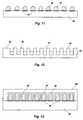
- FIG. 12depicts a surface of a third embodiment of the substrate mold of the present invention having a plurality of rectangular cross-sectional shaped cavities formed therein;
- FIG. 13depicts the substrate mold of FIG. 12 having solder paste in the rectangular cavities in contact with a second substrate
- FIG. 14depicts the second substrate of FIG. 13 having the rectangularly shaped solder paste thereon after the substrate mold has been removed from the substrate of the third embodiment of the invention by the heating thereof;
- FIG. 15depicts the second substrate after the heating of the solder paste thereon to form solder balls
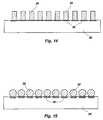
- FIG. 16depicts a fourth embodiment of a substrate mold of the present invention having a plurality of cavities in a surface thereof and a plurality of heating elements on the other surface thereof;
- FIG. 17depicts the substrate mold of FIG. 16 having solder paste in the cavities formed in a surface thereof.
- FIG. 18depicts the other side of the substrate mold of FIG. 16 illustrating the plurality of heating elements thereon along section line 18 — 18 of drawing FIG. 17 .
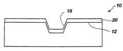
- FIGS. 1A-1DIllustrated in drawing FIGS. 1A-1D is a method for fabricating the semiconductor substrate to form metal bumps or metal traces, or both, on the surface of a secondary substrate.
- a semiconductor substratetypically a flat planar substrate having a flat planar upper surface, a flat planar lower surface, and a plurality of planar sides forming the periphery of the substrate, is selected to serve as a bump-forming substrate mold 10 .
- the semiconductor substratemay be of any desired size and geometric shape suitable for use with an associated semiconductor device.
- the semiconductor substrateis selected from a semiconductor base material such as silicon, gallium arsenide, silicon on insulator, which may include silicon on glass or sapphire, or other well-known semiconductor substrate materials, as well as other similar types of materials, which are capable of being precisely micromachined and having a coefficient of thermal expansion (CTE) similar to that of the semiconductor materials.
- a silicon substrateis used for substrate mold 10 , although any of the other base materials may be freely substituted therefor.
- the silicon substrateis aligned such that the flat, planar substrate upper surface 12 of substrate mold 10 defines the ⁇ 100> plane of the substrate mold 10 which mates with a semiconductor device (not shown). As is shown in drawing FIG.
- the flat, planar substrate upper surface 12 of substrate mold 10has a first protective mask layer 14 located thereon.
- the first protective mask layer 14serves to protect the surface of substrate mold 10 when a subsequent etch is performed to make the cavities or apertures in the flat, planar substrate upper surface 12 .
- First protective mask layer 14may be selected from particular etch-resistant materials such as nitride, oxide, or a hardened polymer spin-on mask.
- Substrate mold 10typically has a thickness of about 25 to 28 mils.
- a photoresist 16is applied over the surface of mask layer 14 and then exposed through a mask to define openings exposing the selected cavity locations to be formed in the flat, planar substrate upper surface 12 .
- a sufficient amount of semiconductor materialis removed by an anisotropic etching from the exposed portion of the flat, planar substrate upper surface 12 after penetration of the exposed portion of first protective mask layer 14 , thereby forming at least one cavity 18 .
- the cavity 18has walls sloped at 54° relative to the ⁇ 100> plane of the substrate mold 10 .
- the anisotropic etchantmay be, for example, KOH, or other etchant materials well known to those skilled in the art. Further, if straight walls are desired, a dry etch using a plasma etch apparatus may be used to form cavity 18 .
- first protective mask layer 14is removed using a dry-etch process that is selective to removing first protective mask layer 14 only and not removing any of the underlying silicon either in the cavity 18 thus formed or on the flat, planar substrate upper surface 12 of substrate mold 10 .
- first protective mask layer 14is silicon dioxide
- a removal substancesuch as phosphoric acid may be used.
- a release layer 20is formed over the entire flat, planar substrate upper surface 12 of substrate mold 10 , particularly covering cavity 18 .
- Release layer 20is selected from a material that is relatively nonwettable to metal solder. Such materials include silicon dioxide or silicon nitride, which can be applied using a chemical vapor deposition process. Other materials that are relatively nonwettable to metal solder may also be used, such as nonwettable polymers or the like. The result in structure is depicted in drawing FIG. 1 D.
- FIGS. 1A-Dillustrate only a single cavity 18 , it is intended that a plurality of cavities be formed in an array across substrate mold 10 .
- An example of a solder ball forming mold or substrate mold 10 that has such a plurality of cavities 18is depicted in drawing FIG. 2 .
- Release layer 20is applied and utilized to minimize the wetting of solder paste on the substrate mold 10 when the assembly is heated in order to transfer the solder onto the bumps of the secondary surface.
- Solder pasteis applied, as shown in drawing FIG. 3, by use of an applicator 22 , such as a squeegee, that is passed across the surface of substrate mold 10 , pressing a metal solder paste 24 into the plurality of cavities 18 and wiping the excess paste away.
- the solder paste 24fills cavities 18 , thus forming frustroconically shaped solder bumps 26 (shown in FIGS. 3 and 4 ).
- metal soldermay be used. The most widely employed types include a lead-tin combination. Other types of metal solder may include, but are not limited to, lead-silver, lead-tin-silver, lead-tin-indium, indium-tin, indium-lead, or any paste using copper or gold in combination with the lead or tin. For example, a lead-tin solder paste having a 63/37 weight ratio has a eutectic temperature of 183° C. Another type of lead-tin paste that has a 95/5 weight ratio has a eutectic temperature of about 350° C.
- solder paste 24is applied to the flat, planar substrate upper surface 12 of substrate mold 10 , the entire assembly is heated to a temperature sufficient enough to slightly melt the metal solder paste in order to begin the formation of the solder bumps to be transferred.
- substrate mold 10is inverted and applied to the surface of a carrier substrate 28 , which may comprise a semiconductor device (die), wafer, or flexible substrate, such as a flex tape.
- the assembly of the substrate mold 10 and carrier substrate 28is heated to a sufficiently high enough temperature to cause solder bumps 26 to slightly reflow and release from the release layer 20 formed on substrate mold 10 .
- Substrate mold 10is then removed and solder bumps 26 adhere to bond pads, terminal pads or other conductive, solder wettable sites 30 on carrier substrate 28 , as shown in drawing FIG. 5 .
- an additional reflow stepmay be performed that causes solder bumps 26 to form into approximately spherically shaped solder balls 32 attached to conductive solder wettable sites 30 as depicted in drawing FIG. 6 .
- solder pasteupon heating reflow, draws into a substantially spherical shape and is held together by the surface tension of the solder material to form approximately spherically shaped solder ball 32 or a truncated spherical ball (not shown).
- solder balls or bumps 32are formed in drawing FIG. 4, it is also possible to form metal traces using substrate mold 10 .
- the same type of patterning and etch steps as described with respect to FIGS. 1A-1Bwould be followed, but would include a layout that would form metal traces or channels.
- a solder mold systemis depicted in drawing FIG. 7 which incorporates the substrate mold 10 shown in drawing FIGS. 1-6.
- the mold systemincludes solder applicator 22 for spreading metal solder paste 24 as dispensed by metal paste dispenser 52 .
- the substrate mold 10is mated to a secondary substrate, as shown in drawing FIG. 4, and then placed in a low-temperature metal paste reflow oven 54 to melt the paste to a sufficient enough consistency to form self-supported bumps and has sufficient enough tackiness to wet the conductive gates on the carrier substrate 28 .
- FIG. 8an alternative embodiment of a substrate mold 40 of the present invention is illustrated.
- the substrate mold 40is similar to the substrate mold 10 described hereinbefore as to construction and methods of construction except that the cavities 18 formed therein are hemispherically shaped.
- the first protective mask layer 14 used to form the plurality of cavities 18is present on portions of the flat, planar upper surface 42 of the substrate mold 40 .
- the substrate mold 40may include a release layer 20 to aid in the release of the solder paste contained within the hemispherical cavities 18 .
- solder paste 24is applied to flat, planar upper surface 42 of substrate mold 40 as described herein with respect to substrate mold 10 illustrated in drawing FIG. 3, the entire assembly of the substrate mold 40 and carrier substrate 28 having conductive sites or bond pads 30 located thereon for the solder paste 24 to be applied is heated to a temperature sufficient enough to slightly melt the metal solder paste 24 in order to begin the formation of the solder bumps to be transferred.
- the assembly of the substrate mold 40 and the carrier substrate 28is inverted so that the solder paste 24 in cavities 18 is applied to the conductive sites 30 on the surface of the carrier substrate 28 , which may comprise a semiconductor device (die), wafer, or flexible substrate, such as a flex tape.
- the assembly of the substrate mold 40 and carrier substrate 28is heated to a sufficiently high enough temperature to cause solder bumps 26 to slightly reflow and release from the release layer 20 formed on substrate mold 40 .
- Substrate mold 40is then removed and solder bumps 26 adhere to the conductive sites, bond pads, terminal pads or other conductive, solder wettable sites 30 on carrier substrate 28 , as shown in drawing FIG. 10 .
- an additional reflow stepmay be performed that causes solder bumps 26 to form into approximately spherically shaped solder balls 32 attached to conductive sites 30 as depicted in drawing FIG. 11 .
- solder pasteupon heating reflow, draws into a substantially spherical shape and is held together by the surface tension of the solder material to form approximately spherically shaped solder balls 32 or truncated spheres.
- FIG. 12an alternative embodiment of a substrate mold 50 of the present invention is illustrated.
- the substrate mold 50is similar to the substrate molds 10 and 40 described hereinbefore as to construction and methods of construction except that the cavities 18 formed therein are generally rectangular, or square shaped (shown in dashed lines).
- the first protective mask layer 14 used to form the plurality of cavities 18 present on portions of the flat, planar upper surface 42 of the substrate mold 50is not illustrated.
- the substrate mold 50may include a release layer 20 to aid in the release of the solder paste contained within the hemispherical cavities 18 . Referring to drawing FIG.
- the entire assembly of the substrate mold 50 and carrier substrate 28 having conductive sites or bond pads 30 located thereon for the solder paste 24 to be appliedis heated to a temperature sufficiently high enough to slightly melt the metal solder paste 24 in order to begin the formation of the solder bumps to be transferred.
- the assembly of the substrate mold 50 and the carrier substrate 28is inverted so that the solder paste 24 is applied to the conductive sites 30 on the surface of the a carrier substrate 28 , which may comprise a semiconductor device (die), wafer, or flexible substrate, such as a flex tape.
- the assembly of the substrate mold 50 and carrier substrate 28is heated to a sufficiently high enough temperature to cause solder bumps 26 to slightly reflow and release from the release layer 20 formed on substrate mold 50 .
- Substrate mold 50is then removed and solder bumps 26 adhere to the conductive sites, bond pads, terminal pads or other conductive, solder wettable sites 30 on carrier substrate 28 , as shown in drawing FIG. 14 .
- an additional reflow stepmay be performed that causes solder bumps 26 to form into approximately spherically shaped solder balls 32 attached to conductive sites 30 as depicted in drawing FIG. 15 .
- solder pasteupon heating reflow, draws into a substantially spherical shape and is held together by the surface tension of the solder material to form approximately spherically shaped solder balls 32 .
- the substrate mold 100is similar to the substrate molds 10 , 40 , and 50 described hereinbefore.
- the substrate mold 100includes cavities 18 having any desired shape as described herein in the flat, planar substrate upper surface 12 and includes electrical resistance heating strips 66 located on the bottom thereof for the heating of the substrate mold 100 with electrical conductor 68 connected thereto.
- the bottom surface of the substrate mold 100includes a coating 62 thereon to electrically insulate the heating strips 66 from the substrate mold 100 .
- the heating strips 66may be of any desired geometrical configuration to cover the bottom surface of the substrate mold 100 to uniformly heat the mold 100 and the solder paste 24 located in the cavities 18 thereof.
- the electrical conductor 68may be any desired shape and have any desired location for connection to the heating strips 66 .
- the electrical conductor 68is covered with an insulation layer 70 located thereover.
- an insulative coating 64 of any suitable typeis provided in areas or portions of the bottom surface of the substrate mold 100 not having a heating strip 66 located thereon.
- the substrate mold 100is illustrated having solder paste 24 located in cavities 18 having release layer 20 therein.
- a carrier substrate 28(see FIG. 4) is applied to the substrate mold 100 , the assembly of the substrate mold 100 and carrier substrate 28 inverted, and the electrical resistance heating strips 66 on the substrate mold 100 actuated to heat the solder paste 24 to transfer the same to the carrier substrate 28 .
- the carrier substrate 28is further heated to cause the solder paste to adhere to the conductive sites 30 on the carrier substrate 28 to substantially form solder balls 32 thereon.
- the electrical resistance heating strips 66 and electrical conductor 68are illustrated.
- the heating strips 66may be of any desired shape to substantially uniformly heat the substrate mold 100 .
- the electrical conductor 68may be any desired shape to electrically connect to the heating strips 66 .
- any desired connectormay be used to electrically connect the electrical conductor 68 to a source of electrical power.
- Substrate molds 10 , 40 , 50 and 100 described hereinare useful in forming contact bumps for many applications.
- One applicationis the formation of flexible connecting tape that requires bumps for interconnection of traces on the tape to a die or other element.
- the micromachining of substrate mold 10provides a much more accurate means for placing the solder ball shaped bumps over the prior art methods of merely placing bumps on top of a screen and then having the screen place the bumps in a proper alignment. Further, the solder ball shaped bumps have a more uniform volume and shape as the cavity dimensions in the semiconductor mold provide a substantially precise control over the formation of the solder ball shaped bumps.
- solder ball shaped bump applicationis useful in chip scale packages (CSP) or in fine ball grid array (FBGA) packages.
- CSPchip scale packages
- FBGAfine ball grid array
- the metal trace interconnect and the bump contactmay be used in any type of semiconductor device such as a memory storage device. These memory storage devices can range from read-only memory (ROM) and random access memory (RAM) to exotic types of memory such as video memory and the memory used in computer systems. Additionally, the application of this metal trace interconnect and bump contact structure can be utilized in micro-processor packages that are used in computer systems as well as in other types of systems, and other types of single processing devices and support chips normally used in electronic devices. These electronic devices range from cellular phones to microwave systems, to automobiles and even to programmable wrist watches.
- ROMread-only memory
- RAMrandom access memory
- the application of this metal trace interconnect and bump contact structurecan be utilized in micro-processor packages that are used in computer systems as well as in other types of systems, and other types of single processing devices and support chips normally used in electronic devices. These electronic devices range from cellular phones to microwave systems, to automobiles and even to programmable wrist watches.
Landscapes
- Engineering & Computer Science (AREA)
- Manufacturing & Machinery (AREA)
- Microelectronics & Electronic Packaging (AREA)
- Computer Hardware Design (AREA)
- Power Engineering (AREA)
- Physics & Mathematics (AREA)
- Condensed Matter Physics & Semiconductors (AREA)
- General Physics & Mathematics (AREA)
- Electric Connection Of Electric Components To Printed Circuits (AREA)
- Wire Bonding (AREA)
Abstract
Description
Claims (23)
Priority Applications (4)
| Application Number | Priority Date | Filing Date | Title |
|---|---|---|---|
| US09/942,246US6612027B2 (en) | 1999-09-02 | 2001-08-29 | Method for forming metal contacts on a substrate |
| US10/639,348US7131195B2 (en) | 1999-09-02 | 2003-08-12 | Method for forming metal contacts on a substrate |
| US10/971,392US7157364B2 (en) | 1999-09-02 | 2004-10-21 | Method for forming metal contacts on a substrate |
| US11/246,348US20060027632A1 (en) | 1999-09-02 | 2005-10-07 | Method for forming metal contacts on a substrate |
Applications Claiming Priority (2)
| Application Number | Priority Date | Filing Date | Title |
|---|---|---|---|
| US09/389,316US6295730B1 (en) | 1999-09-02 | 1999-09-02 | Method and apparatus for forming metal contacts on a substrate |
| US09/942,246US6612027B2 (en) | 1999-09-02 | 2001-08-29 | Method for forming metal contacts on a substrate |
Related Parent Applications (1)
| Application Number | Title | Priority Date | Filing Date |
|---|---|---|---|
| US09/389,316ContinuationUS6295730B1 (en) | 1999-09-02 | 1999-09-02 | Method and apparatus for forming metal contacts on a substrate |
Related Child Applications (1)
| Application Number | Title | Priority Date | Filing Date |
|---|---|---|---|
| US10/639,348ContinuationUS7131195B2 (en) | 1999-09-02 | 2003-08-12 | Method for forming metal contacts on a substrate |
Publications (2)
| Publication Number | Publication Date |
|---|---|
| US20020004981A1 US20020004981A1 (en) | 2002-01-17 |
| US6612027B2true US6612027B2 (en) | 2003-09-02 |
Family
ID=23537751
Family Applications (5)
| Application Number | Title | Priority Date | Filing Date |
|---|---|---|---|
| US09/389,316Expired - Fee RelatedUS6295730B1 (en) | 1999-09-02 | 1999-09-02 | Method and apparatus for forming metal contacts on a substrate |
| US09/942,246Expired - LifetimeUS6612027B2 (en) | 1999-09-02 | 2001-08-29 | Method for forming metal contacts on a substrate |
| US10/639,348Expired - LifetimeUS7131195B2 (en) | 1999-09-02 | 2003-08-12 | Method for forming metal contacts on a substrate |
| US10/971,392Expired - LifetimeUS7157364B2 (en) | 1999-09-02 | 2004-10-21 | Method for forming metal contacts on a substrate |
| US11/246,348AbandonedUS20060027632A1 (en) | 1999-09-02 | 2005-10-07 | Method for forming metal contacts on a substrate |
Family Applications Before (1)
| Application Number | Title | Priority Date | Filing Date |
|---|---|---|---|
| US09/389,316Expired - Fee RelatedUS6295730B1 (en) | 1999-09-02 | 1999-09-02 | Method and apparatus for forming metal contacts on a substrate |
Family Applications After (3)
| Application Number | Title | Priority Date | Filing Date |
|---|---|---|---|
| US10/639,348Expired - LifetimeUS7131195B2 (en) | 1999-09-02 | 2003-08-12 | Method for forming metal contacts on a substrate |
| US10/971,392Expired - LifetimeUS7157364B2 (en) | 1999-09-02 | 2004-10-21 | Method for forming metal contacts on a substrate |
| US11/246,348AbandonedUS20060027632A1 (en) | 1999-09-02 | 2005-10-07 | Method for forming metal contacts on a substrate |
Country Status (1)
| Country | Link |
|---|---|
| US (5) | US6295730B1 (en) |
Cited By (8)
| Publication number | Priority date | Publication date | Assignee | Title |
|---|---|---|---|---|
| US20050085063A1 (en)* | 1999-09-02 | 2005-04-21 | Salman Akram | Method for forming metal contacts on a substrate |
| US20050158918A1 (en)* | 2001-06-30 | 2005-07-21 | Liu Jwei W. | Masking layer in substrate cavity |
| US20080165518A1 (en)* | 2005-03-16 | 2008-07-10 | Takashi Ichiryu | Flip Clip Mounting Process And Bump-Forming Process Using Electrically-Conductive Particles |
| US20080175939A1 (en)* | 2007-01-22 | 2008-07-24 | International Business Machines Corporation | Techniques for forming interconnects |
| US20080197173A1 (en)* | 2005-05-24 | 2008-08-21 | Matsushita Electric Industrial Co., Ltd. | Method for Forming Solder Bump and Method for Mounting Semiconductor Device |
| US20090001248A1 (en)* | 2007-06-27 | 2009-01-01 | Farinelli Matthew J | Methods of Creating Molds of Variable Solder Volumes for Flip Attach |
| US20090078746A1 (en)* | 2006-03-28 | 2009-03-26 | Seiji Karashima | Bump forming method and bump forming apparatus |
| US20110201195A1 (en)* | 2005-04-06 | 2011-08-18 | Panasonic Corporation | Flip chip mounting method and bump forming method |
Families Citing this family (65)
| Publication number | Priority date | Publication date | Assignee | Title |
|---|---|---|---|---|
| US6409073B1 (en)* | 1998-07-15 | 2002-06-25 | Fraunhofer-Gesellschaft Zur Foerderung Der Angewandten Forschung E.V. | Method for transfering solder to a device and/or testing the device |
| US7156361B1 (en)* | 1999-09-02 | 2007-01-02 | Micron Technology, Inc. | Method and apparatus for forming metal contacts on a substrate |
| US7115986B2 (en) | 2001-05-02 | 2006-10-03 | Micron Technology, Inc. | Flexible ball grid array chip scale packages |
| SG122743A1 (en) | 2001-08-21 | 2006-06-29 | Micron Technology Inc | Microelectronic devices and methods of manufacture |
| SG104293A1 (en) | 2002-01-09 | 2004-06-21 | Micron Technology Inc | Elimination of rdl using tape base flip chip on flex for die stacking |
| SG115455A1 (en) | 2002-03-04 | 2005-10-28 | Micron Technology Inc | Methods for assembly and packaging of flip chip configured dice with interposer |
| SG121707A1 (en) | 2002-03-04 | 2006-05-26 | Micron Technology Inc | Method and apparatus for flip-chip packaging providing testing capability |
| SG115456A1 (en) | 2002-03-04 | 2005-10-28 | Micron Technology Inc | Semiconductor die packages with recessed interconnecting structures and methods for assembling the same |
| US6975035B2 (en) | 2002-03-04 | 2005-12-13 | Micron Technology, Inc. | Method and apparatus for dielectric filling of flip chip on interposer assembly |
| SG111935A1 (en) | 2002-03-04 | 2005-06-29 | Micron Technology Inc | Interposer configured to reduce the profiles of semiconductor device assemblies and packages including the same and methods |
| SG115459A1 (en) | 2002-03-04 | 2005-10-28 | Micron Technology Inc | Flip chip packaging using recessed interposer terminals |
| KR100481216B1 (en)* | 2002-06-07 | 2005-04-08 | 엘지전자 주식회사 | Ball Grid Array Package And Method Of Fabricating The Same |
| US6960518B1 (en) | 2002-07-19 | 2005-11-01 | Taiwan Semiconductor Manufacturing Co., Ltd. | Buildup substrate pad pre-solder bump manufacturing |
| US20040036170A1 (en) | 2002-08-20 | 2004-02-26 | Lee Teck Kheng | Double bumping of flexible substrate for first and second level interconnects |
| DE10339609A1 (en)* | 2003-08-28 | 2005-03-24 | Forschungszentrum Karlsruhe Gmbh | Oligonucleotide, method and system for the detection of antibiotic resistance-mediating genes in microorganisms by means of real-time PCR |
| DE10351720B4 (en)* | 2003-10-31 | 2005-09-29 | Siemens Ag | Test standard for testing optical detection systems used in SMD mounting and method of making same |
| US20060108402A1 (en)* | 2004-11-19 | 2006-05-25 | Tessera, Inc. | Solder ball formation and transfer method |
| DE102004062212A1 (en)* | 2004-12-23 | 2006-07-13 | Texas Instruments Deutschland Gmbh | Electronic device, chip contacting method and contacting device |
| US20070152023A1 (en)* | 2005-12-30 | 2007-07-05 | Semx Corporation | Solder deposit method on electronic packages for post-connection process |
| US7946470B2 (en)* | 2005-12-30 | 2011-05-24 | Semx Corporation | Method for depositing solder material on an electronic component part using separators |
| JP2007227558A (en)* | 2006-02-22 | 2007-09-06 | Nec Electronics Corp | Apparatus and method of manufacturing semiconductor device |
| US20080029686A1 (en)* | 2006-08-04 | 2008-02-07 | International Business Machines Corporation | Precision fabricated silicon mold |
| US7494913B2 (en)* | 2006-08-31 | 2009-02-24 | Intel Corporation | Microball placement solutions |
| US7493186B2 (en)* | 2006-12-20 | 2009-02-17 | International Business Machines Corporation | Method and algorithm for the control of critical dimensions in a thermal flow process |
| US7931249B2 (en)* | 2007-02-01 | 2011-04-26 | International Business Machines Corporation | Reduced friction molds for injection molded solder processing |
| TW200839903A (en)* | 2007-03-21 | 2008-10-01 | Advanced Semiconductor Eng | Method for manufacturing electrical connections in wafer |
| US8148255B2 (en)* | 2007-09-18 | 2012-04-03 | International Business Machines Corporation | Techniques for forming solder bump interconnects |
| US20090108442A1 (en)* | 2007-10-25 | 2009-04-30 | International Business Machines Corporation | Self-assembled stress relief interface |
| KR20090076048A (en)* | 2008-01-07 | 2009-07-13 | 세크론 주식회사 | A template for forming solder bumps, a method of manufacturing the same, and a method of inspecting the solder bumps using the same |
| KR101032085B1 (en)* | 2008-12-12 | 2011-05-02 | 엘아이지에이디피 주식회사 | Template for solder bump formation and manufacturing method thereof |
| US20110079702A1 (en)* | 2009-10-06 | 2011-04-07 | International Business Machines Corporation | Forming a protective layer on a mold and mold having a protective layer |
| TWI402003B (en)* | 2009-10-16 | 2013-07-11 | Princo Corp | Metal structure of flexible multi-layer substrate and manufacturing method thereof |
| TWI392069B (en)* | 2009-11-24 | 2013-04-01 | Advanced Semiconductor Eng | Package structure and packaging process thereof |
| US8507325B2 (en)* | 2010-01-28 | 2013-08-13 | International Business Machines Corporation | Co-axial restraint for connectors within flip-chip packages |
| TWI446420B (en) | 2010-08-27 | 2014-07-21 | Advanced Semiconductor Eng | Carrier separation method for semiconductor process |
| TWI445152B (en) | 2010-08-30 | 2014-07-11 | Advanced Semiconductor Eng | Semiconductor structure and method for manufacturing the same |
| US9007273B2 (en) | 2010-09-09 | 2015-04-14 | Advances Semiconductor Engineering, Inc. | Semiconductor package integrated with conformal shield and antenna |
| TWI434387B (en) | 2010-10-11 | 2014-04-11 | Advanced Semiconductor Eng | Semiconductor element having a via and package having a semiconductor element with a via and method for making the same |
| TWI527174B (en) | 2010-11-19 | 2016-03-21 | 日月光半導體製造股份有限公司 | Package having semiconductor device |
| TWI445155B (en) | 2011-01-06 | 2014-07-11 | Advanced Semiconductor Eng | Stacked semiconductor package and method for making the same |
| US8853819B2 (en) | 2011-01-07 | 2014-10-07 | Advanced Semiconductor Engineering, Inc. | Semiconductor structure with passive element network and manufacturing method thereof |
| US8541883B2 (en) | 2011-11-29 | 2013-09-24 | Advanced Semiconductor Engineering, Inc. | Semiconductor device having shielded conductive vias |
| US8534533B2 (en)* | 2012-01-19 | 2013-09-17 | Raytheon Company | Solder paste transfer process |
| US8975157B2 (en) | 2012-02-08 | 2015-03-10 | Advanced Semiconductor Engineering, Inc. | Carrier bonding and detaching processes for a semiconductor wafer |
| US8963316B2 (en) | 2012-02-15 | 2015-02-24 | Advanced Semiconductor Engineering, Inc. | Semiconductor device and method for manufacturing the same |
| US8770462B2 (en) | 2012-03-14 | 2014-07-08 | Raytheon Company | Solder paste transfer process |
| US8786060B2 (en) | 2012-05-04 | 2014-07-22 | Advanced Semiconductor Engineering, Inc. | Semiconductor package integrated with conformal shield and antenna |
| US9153542B2 (en) | 2012-08-01 | 2015-10-06 | Advanced Semiconductor Engineering, Inc. | Semiconductor package having an antenna and manufacturing method thereof |
| US8937387B2 (en) | 2012-11-07 | 2015-01-20 | Advanced Semiconductor Engineering, Inc. | Semiconductor device with conductive vias |
| US8952542B2 (en) | 2012-11-14 | 2015-02-10 | Advanced Semiconductor Engineering, Inc. | Method for dicing a semiconductor wafer having through silicon vias and resultant structures |
| US9406552B2 (en) | 2012-12-20 | 2016-08-02 | Advanced Semiconductor Engineering, Inc. | Semiconductor device having conductive via and manufacturing process |
| US8841751B2 (en) | 2013-01-23 | 2014-09-23 | Advanced Semiconductor Engineering, Inc. | Through silicon vias for semiconductor devices and manufacturing method thereof |
| US9978688B2 (en) | 2013-02-28 | 2018-05-22 | Advanced Semiconductor Engineering, Inc. | Semiconductor package having a waveguide antenna and manufacturing method thereof |
| US9089268B2 (en) | 2013-03-13 | 2015-07-28 | Advanced Semiconductor Engineering, Inc. | Neural sensing device and method for making the same |
| US8987734B2 (en) | 2013-03-15 | 2015-03-24 | Advanced Semiconductor Engineering, Inc. | Semiconductor wafer, semiconductor process and semiconductor package |
| US9173583B2 (en) | 2013-03-15 | 2015-11-03 | Advanced Semiconductor Engineering, Inc. | Neural sensing device and method for making the same |
| TW201508848A (en)* | 2013-08-23 | 2015-03-01 | Chipmos Technologies Inc | Planting device and planting method thereof |
| WO2015052780A1 (en)* | 2013-10-08 | 2015-04-16 | リンテック株式会社 | Method of manufacturing electronic component mounting body |
| US9263329B2 (en)* | 2014-03-19 | 2016-02-16 | Intel Corporation | Methods of connecting a first electronic package to a second electronic package |
| CN104117747B (en)* | 2014-07-08 | 2016-05-11 | 宜兴市吉泰电子有限公司 | Electronic encapsulation shell lead welding method |
| CN105397096B (en)* | 2015-11-30 | 2017-07-28 | 苏州瑞而美光电科技有限公司 | Mark the preparation facilities of footpath BGA package metal soldered ball |
| CN109148306A (en)* | 2018-09-04 | 2019-01-04 | 深圳市诚朗科技有限公司 | A kind of Rework Technics of BGA Package component |
| DE102019116153A1 (en) | 2019-06-13 | 2020-12-17 | Kennametal Inc. | Armor plate, armor plate composite and armor |
| DE102022100599A1 (en) | 2022-01-12 | 2023-08-03 | Kennametal Inc. | Armor Plate, Armor Plate Composite, and Armor |
| CN115440650B (en)* | 2022-09-20 | 2025-08-01 | 中国科学院光电技术研究所 | Pin type substrate holder and preparation method thereof |
Citations (22)
| Publication number | Priority date | Publication date | Assignee | Title |
|---|---|---|---|---|
| US2979773A (en) | 1959-08-26 | 1961-04-18 | Honeywell Regulator Co | Molding apparatus |
| US4125441A (en) | 1978-01-30 | 1978-11-14 | General Dynamics Corporation | Isolated bump circuitry on tape utilizing electroforming |
| US4141782A (en) | 1978-01-30 | 1979-02-27 | General Dynamics Corporation | Bump circuits on tape utilizing chemical milling |
| US4649415A (en) | 1985-01-15 | 1987-03-10 | National Semiconductor Corporation | Semiconductor package with tape mounted die |
| US4807021A (en) | 1986-03-10 | 1989-02-21 | Kabushiki Kaisha Toshiba | Semiconductor device having stacking structure |
| US4906823A (en) | 1987-06-05 | 1990-03-06 | Hitachi, Ltd. | Solder carrier, manufacturing method thereof and method of mounting semiconductor devices by utilizing same |
| US4967261A (en) | 1987-07-30 | 1990-10-30 | Mitsubishi Denki Kabushiki Kaisha | Tape carrier for assembling an IC chip on a substrate |
| US5045657A (en) | 1989-02-23 | 1991-09-03 | Daimler-Benz Ag | Actuating device for the mechanical positive actuation of a pressure-response switch |
| US5244143A (en) | 1992-04-16 | 1993-09-14 | International Business Machines Corporation | Apparatus and method for injection molding solder and applications thereof |
| US5371406A (en) | 1992-12-16 | 1994-12-06 | Kabushiki Kaisha Toshiba | Semiconductor device |
| US5381848A (en) | 1993-09-15 | 1995-01-17 | Lsi Logic Corporation | Casting of raised bump contacts on a substrate |
| US5491415A (en) | 1992-03-05 | 1996-02-13 | Picker International, Inc. | Magnetic resonance scanner with improved packaging for circuitry within the magnetic field |
| US5607099A (en) | 1995-04-24 | 1997-03-04 | Delco Electronics Corporation | Solder bump transfer device for flip chip integrated circuit devices |
| US5643831A (en) | 1994-01-20 | 1997-07-01 | Fujitsu Limited | Process for forming solder balls on a plate having apertures using solder paste and transferring the solder balls to semiconductor device |
| US5718361A (en) | 1995-11-21 | 1998-02-17 | International Business Machines Corporation | Apparatus and method for forming mold for metallic material |
| US5718367A (en) | 1995-11-21 | 1998-02-17 | International Business Machines Corporation | Mold transfer apparatus and method |
| US5775569A (en) | 1996-10-31 | 1998-07-07 | Ibm Corporation | Method for building interconnect structures by injection molded solder and structures built |
| US5984164A (en)* | 1997-10-31 | 1999-11-16 | Micron Technology, Inc. | Method of using an electrically conductive elevation shaping tool |
| US6003757A (en) | 1998-04-30 | 1999-12-21 | International Business Machines Corporation | Apparatus for transferring solder bumps and method of using |
| US6025258A (en) | 1994-01-20 | 2000-02-15 | Fujitsu Limited | Method for fabricating solder bumps by forming solder balls with a solder ball forming member |
| US6139972A (en) | 1998-10-26 | 2000-10-31 | Agilent Technologies Inc. | Solder paste containment device |
| US6271110B1 (en) | 1994-01-20 | 2001-08-07 | Fujitsu Limited | Bump-forming method using two plates and electronic device |
Family Cites Families (26)
| Publication number | Priority date | Publication date | Assignee | Title |
|---|---|---|---|---|
| US3349480A (en)* | 1962-11-09 | 1967-10-31 | Ibm | Method of forming through hole conductor lines |
| US3516155A (en) | 1967-02-02 | 1970-06-23 | Bunker Ramo | Method and apparatus for assembling electrical components |
| US4412642A (en) | 1982-03-15 | 1983-11-01 | Western Electric Co., Inc. | Cast solder leads for leadless semiconductor circuits |
| US5046657A (en)* | 1988-02-09 | 1991-09-10 | National Semiconductor Corporation | Tape automated bonding of bumped tape on bumped die |
| US5578526A (en) | 1992-03-06 | 1996-11-26 | Micron Technology, Inc. | Method for forming a multi chip module (MCM) |
| US5445994A (en) | 1994-04-11 | 1995-08-29 | Micron Technology, Inc. | Method for forming custom planar metal bonding pad connectors for semiconductor dice |
| US5593918A (en)* | 1994-04-22 | 1997-01-14 | Lsi Logic Corporation | Techniques for forming superconductive lines |
| US5872051A (en)* | 1995-08-02 | 1999-02-16 | International Business Machines Corporation | Process for transferring material to semiconductor chip conductive pads using a transfer substrate |
| DE19533169C2 (en) | 1995-09-08 | 2002-02-07 | Fraunhofer Ges Forschung | solder deposit |
| JP3385872B2 (en) | 1995-12-25 | 2003-03-10 | 三菱電機株式会社 | Solder supply method and solder supply apparatus |
| JPH10163368A (en)* | 1996-12-02 | 1998-06-19 | Fujitsu Ltd | Semiconductor device manufacturing method and semiconductor device |
| US6293456B1 (en)* | 1997-05-27 | 2001-09-25 | Spheretek, Llc | Methods for forming solder balls on substrates |
| KR100278219B1 (en)* | 1997-06-18 | 2001-01-15 | 클라크 3세 존 엠. | Method of making flip chip and bga interconnections |
| US6105852A (en)* | 1998-02-05 | 2000-08-22 | International Business Machines Corporation | Etched glass solder bump transfer for flip chip integrated circuit devices |
| US6056191A (en)* | 1998-04-30 | 2000-05-02 | International Business Machines Corporation | Method and apparatus for forming solder bumps |
| US6046657A (en)* | 1998-08-21 | 2000-04-04 | Lucent Technologies Inc. | Magnetostrictive surface acoustic wave device and microelectronic circuit including same |
| CN1142536C (en)* | 1998-10-30 | 2004-03-17 | 松下电器产业株式会社 | Display device with plasma display panel |
| US6523736B1 (en)* | 1998-12-11 | 2003-02-25 | Micron Technology, Inc. | Methods and apparatus for forming solder balls |
| US6295730B1 (en)* | 1999-09-02 | 2001-10-02 | Micron Technology, Inc. | Method and apparatus for forming metal contacts on a substrate |
| US6371406B1 (en)* | 1999-11-19 | 2002-04-16 | Bruce Alan Corcoran | Progressive 3-axis multi-variable propulsion vectoring aerial and spacecraft vehicle |
| US6244143B1 (en)* | 1999-11-29 | 2001-06-12 | Thomas J. Reisdorph | Lathe |
| JP2003174692A (en)* | 2001-12-07 | 2003-06-20 | Sony Corp | Display device |
| KR100450207B1 (en)* | 2002-08-22 | 2004-09-24 | 삼성에스디아이 주식회사 | Plasma display device |
| KR100581863B1 (en)* | 2003-10-09 | 2006-05-22 | 삼성에스디아이 주식회사 | Plasma display device |
| US7570489B1 (en)* | 2008-01-21 | 2009-08-04 | Wincomm Corporation | Heat dissipation system for digital electronic signboard |
| US8313068B2 (en)* | 2008-05-08 | 2012-11-20 | Samsung Electronics Co., Ltd. | Lifting device for display apparatus |
- 1999
- 1999-09-02USUS09/389,316patent/US6295730B1/ennot_activeExpired - Fee Related
- 2001
- 2001-08-29USUS09/942,246patent/US6612027B2/ennot_activeExpired - Lifetime
- 2003
- 2003-08-12USUS10/639,348patent/US7131195B2/ennot_activeExpired - Lifetime
- 2004
- 2004-10-21USUS10/971,392patent/US7157364B2/ennot_activeExpired - Lifetime
- 2005
- 2005-10-07USUS11/246,348patent/US20060027632A1/ennot_activeAbandoned
Patent Citations (23)
| Publication number | Priority date | Publication date | Assignee | Title |
|---|---|---|---|---|
| US2979773A (en) | 1959-08-26 | 1961-04-18 | Honeywell Regulator Co | Molding apparatus |
| US4125441A (en) | 1978-01-30 | 1978-11-14 | General Dynamics Corporation | Isolated bump circuitry on tape utilizing electroforming |
| US4141782A (en) | 1978-01-30 | 1979-02-27 | General Dynamics Corporation | Bump circuits on tape utilizing chemical milling |
| US4649415A (en) | 1985-01-15 | 1987-03-10 | National Semiconductor Corporation | Semiconductor package with tape mounted die |
| US4807021A (en) | 1986-03-10 | 1989-02-21 | Kabushiki Kaisha Toshiba | Semiconductor device having stacking structure |
| US4906823A (en) | 1987-06-05 | 1990-03-06 | Hitachi, Ltd. | Solder carrier, manufacturing method thereof and method of mounting semiconductor devices by utilizing same |
| US4967261A (en) | 1987-07-30 | 1990-10-30 | Mitsubishi Denki Kabushiki Kaisha | Tape carrier for assembling an IC chip on a substrate |
| US5045657A (en) | 1989-02-23 | 1991-09-03 | Daimler-Benz Ag | Actuating device for the mechanical positive actuation of a pressure-response switch |
| US5491415A (en) | 1992-03-05 | 1996-02-13 | Picker International, Inc. | Magnetic resonance scanner with improved packaging for circuitry within the magnetic field |
| US5244143A (en) | 1992-04-16 | 1993-09-14 | International Business Machines Corporation | Apparatus and method for injection molding solder and applications thereof |
| US5371406A (en) | 1992-12-16 | 1994-12-06 | Kabushiki Kaisha Toshiba | Semiconductor device |
| US5381848A (en) | 1993-09-15 | 1995-01-17 | Lsi Logic Corporation | Casting of raised bump contacts on a substrate |
| US5643831A (en) | 1994-01-20 | 1997-07-01 | Fujitsu Limited | Process for forming solder balls on a plate having apertures using solder paste and transferring the solder balls to semiconductor device |
| US6025258A (en) | 1994-01-20 | 2000-02-15 | Fujitsu Limited | Method for fabricating solder bumps by forming solder balls with a solder ball forming member |
| US6271110B1 (en) | 1994-01-20 | 2001-08-07 | Fujitsu Limited | Bump-forming method using two plates and electronic device |
| US5607099A (en) | 1995-04-24 | 1997-03-04 | Delco Electronics Corporation | Solder bump transfer device for flip chip integrated circuit devices |
| US5718361A (en) | 1995-11-21 | 1998-02-17 | International Business Machines Corporation | Apparatus and method for forming mold for metallic material |
| US5718367A (en) | 1995-11-21 | 1998-02-17 | International Business Machines Corporation | Mold transfer apparatus and method |
| US5775569A (en) | 1996-10-31 | 1998-07-07 | Ibm Corporation | Method for building interconnect structures by injection molded solder and structures built |
| US5984164A (en)* | 1997-10-31 | 1999-11-16 | Micron Technology, Inc. | Method of using an electrically conductive elevation shaping tool |
| US6234373B1 (en)* | 1997-10-31 | 2001-05-22 | Micron Technology, Inc. | Electrically conductive elevation shaping tool |
| US6003757A (en) | 1998-04-30 | 1999-12-21 | International Business Machines Corporation | Apparatus for transferring solder bumps and method of using |
| US6139972A (en) | 1998-10-26 | 2000-10-31 | Agilent Technologies Inc. | Solder paste containment device |
Cited By (17)
| Publication number | Priority date | Publication date | Assignee | Title |
|---|---|---|---|---|
| US20050085063A1 (en)* | 1999-09-02 | 2005-04-21 | Salman Akram | Method for forming metal contacts on a substrate |
| US7157364B2 (en)* | 1999-09-02 | 2007-01-02 | Micron Technology, Inc. | Method for forming metal contacts on a substrate |
| US20050158918A1 (en)* | 2001-06-30 | 2005-07-21 | Liu Jwei W. | Masking layer in substrate cavity |
| US7314816B2 (en)* | 2001-06-30 | 2008-01-01 | Texas Instruments Incorporated | Masking layer in substrate cavity |
| US7726545B2 (en)* | 2005-03-16 | 2010-06-01 | Panasonic Corporation | Flip chip mounting process and bump-forming process using electrically-conductive particles as nuclei |
| US20080165518A1 (en)* | 2005-03-16 | 2008-07-10 | Takashi Ichiryu | Flip Clip Mounting Process And Bump-Forming Process Using Electrically-Conductive Particles |
| US20110201195A1 (en)* | 2005-04-06 | 2011-08-18 | Panasonic Corporation | Flip chip mounting method and bump forming method |
| US8283246B2 (en) | 2005-04-06 | 2012-10-09 | Panasonic Corporation | Flip chip mounting method and bump forming method |
| US20080197173A1 (en)* | 2005-05-24 | 2008-08-21 | Matsushita Electric Industrial Co., Ltd. | Method for Forming Solder Bump and Method for Mounting Semiconductor Device |
| CN100501957C (en)* | 2005-05-24 | 2009-06-17 | 松下电器产业株式会社 | Method for forming solder bump and method for mounting semiconductor element |
| US7611040B2 (en)* | 2005-05-24 | 2009-11-03 | Panasonic Corporation | Method for forming solder bump and method for mounting semiconductor device using a solder powder resin composition |
| US20090078746A1 (en)* | 2006-03-28 | 2009-03-26 | Seiji Karashima | Bump forming method and bump forming apparatus |
| US8297488B2 (en)* | 2006-03-28 | 2012-10-30 | Panasonic Corporation | Bump forming method using self-assembling resin and a wall surface |
| US20080175939A1 (en)* | 2007-01-22 | 2008-07-24 | International Business Machines Corporation | Techniques for forming interconnects |
| US7819376B2 (en)* | 2007-01-22 | 2010-10-26 | International Business Machines Corporation | Techniques for forming interconnects |
| US20090001248A1 (en)* | 2007-06-27 | 2009-01-01 | Farinelli Matthew J | Methods of Creating Molds of Variable Solder Volumes for Flip Attach |
| US20090004840A1 (en)* | 2007-06-27 | 2009-01-01 | Farinelli Matthew J | Method of Creating Molds of Variable Solder Volumes for Flip Attach |
Also Published As
| Publication number | Publication date |
|---|---|
| US7157364B2 (en) | 2007-01-02 |
| US7131195B2 (en) | 2006-11-07 |
| US6295730B1 (en) | 2001-10-02 |
| US20040031145A1 (en) | 2004-02-19 |
| US20020004981A1 (en) | 2002-01-17 |
| US20060027632A1 (en) | 2006-02-09 |
| US20050085063A1 (en) | 2005-04-21 |
Similar Documents
| Publication | Publication Date | Title |
|---|---|---|
| US6612027B2 (en) | Method for forming metal contacts on a substrate | |
| US6245594B1 (en) | Methods for forming conductive micro-bumps and recessed contacts for flip-chip technology and method of flip-chip assembly | |
| US6559527B2 (en) | Process for forming cone shaped solder for chip interconnection | |
| US6900079B2 (en) | Method for fabricating a chip scale package using wafer level processing | |
| US6355507B1 (en) | Method of forming overmolded chip scale package and resulting product | |
| US5607099A (en) | Solder bump transfer device for flip chip integrated circuit devices | |
| US5925930A (en) | IC contacts with palladium layer and flexible conductive epoxy bumps | |
| US7156361B1 (en) | Method and apparatus for forming metal contacts on a substrate | |
| KR100265616B1 (en) | Flip Chip Using Conductive Polymer and Dielectric | |
| KR100615024B1 (en) | Carriers and Systems for Testing Bumped Semiconductor Components | |
| KR101411482B1 (en) | Microelectronic device having a compliant terminal mounting part and method of manufacturing the same | |
| US6638638B2 (en) | Hollow solder structure having improved reliability and method of manufacturing same | |
| US20010053567A1 (en) | Method of forming a test insert for interfacing a device containing contact bumps with a test substrate | |
| KR970012964A (en) | A system interconnected by bond material bumps | |
| US6380060B1 (en) | Off-center solder ball attach and methods therefor | |
| US20010008250A1 (en) | Method of forming a solder ball | |
| US5924623A (en) | Diffusion patterned C4 bump pads | |
| US6960518B1 (en) | Buildup substrate pad pre-solder bump manufacturing | |
| JPH10209623A (en) | Method for forming solder bump | |
| JPH06232212A (en) | Printed wiring board, and manufacture thereof |
Legal Events
| Date | Code | Title | Description |
|---|---|---|---|
| STCF | Information on status: patent grant | Free format text:PATENTED CASE | |
| FEPP | Fee payment procedure | Free format text:PAYOR NUMBER ASSIGNED (ORIGINAL EVENT CODE: ASPN); ENTITY STATUS OF PATENT OWNER: LARGE ENTITY | |
| CC | Certificate of correction | ||
| FPAY | Fee payment | Year of fee payment:4 | |
| FPAY | Fee payment | Year of fee payment:8 | |
| FPAY | Fee payment | Year of fee payment:12 | |
| AS | Assignment | Owner name:U.S. BANK NATIONAL ASSOCIATION, AS COLLATERAL AGENT, CALIFORNIA Free format text:SECURITY INTEREST;ASSIGNOR:MICRON TECHNOLOGY, INC.;REEL/FRAME:038669/0001 Effective date:20160426 Owner name:U.S. BANK NATIONAL ASSOCIATION, AS COLLATERAL AGEN Free format text:SECURITY INTEREST;ASSIGNOR:MICRON TECHNOLOGY, INC.;REEL/FRAME:038669/0001 Effective date:20160426 | |
| AS | Assignment | Owner name:MORGAN STANLEY SENIOR FUNDING, INC., AS COLLATERAL AGENT, MARYLAND Free format text:PATENT SECURITY AGREEMENT;ASSIGNOR:MICRON TECHNOLOGY, INC.;REEL/FRAME:038954/0001 Effective date:20160426 Owner name:MORGAN STANLEY SENIOR FUNDING, INC., AS COLLATERAL Free format text:PATENT SECURITY AGREEMENT;ASSIGNOR:MICRON TECHNOLOGY, INC.;REEL/FRAME:038954/0001 Effective date:20160426 | |
| AS | Assignment | Owner name:U.S. BANK NATIONAL ASSOCIATION, AS COLLATERAL AGENT, CALIFORNIA Free format text:CORRECTIVE ASSIGNMENT TO CORRECT THE REPLACE ERRONEOUSLY FILED PATENT #7358718 WITH THE CORRECT PATENT #7358178 PREVIOUSLY RECORDED ON REEL 038669 FRAME 0001. ASSIGNOR(S) HEREBY CONFIRMS THE SECURITY INTEREST;ASSIGNOR:MICRON TECHNOLOGY, INC.;REEL/FRAME:043079/0001 Effective date:20160426 Owner name:U.S. BANK NATIONAL ASSOCIATION, AS COLLATERAL AGEN Free format text:CORRECTIVE ASSIGNMENT TO CORRECT THE REPLACE ERRONEOUSLY FILED PATENT #7358718 WITH THE CORRECT PATENT #7358178 PREVIOUSLY RECORDED ON REEL 038669 FRAME 0001. ASSIGNOR(S) HEREBY CONFIRMS THE SECURITY INTEREST;ASSIGNOR:MICRON TECHNOLOGY, INC.;REEL/FRAME:043079/0001 Effective date:20160426 | |
| AS | Assignment | Owner name:JPMORGAN CHASE BANK, N.A., AS COLLATERAL AGENT, ILLINOIS Free format text:SECURITY INTEREST;ASSIGNORS:MICRON TECHNOLOGY, INC.;MICRON SEMICONDUCTOR PRODUCTS, INC.;REEL/FRAME:047540/0001 Effective date:20180703 Owner name:JPMORGAN CHASE BANK, N.A., AS COLLATERAL AGENT, IL Free format text:SECURITY INTEREST;ASSIGNORS:MICRON TECHNOLOGY, INC.;MICRON SEMICONDUCTOR PRODUCTS, INC.;REEL/FRAME:047540/0001 Effective date:20180703 | |
| AS | Assignment | Owner name:MICRON TECHNOLOGY, INC., IDAHO Free format text:RELEASE BY SECURED PARTY;ASSIGNOR:U.S. BANK NATIONAL ASSOCIATION, AS COLLATERAL AGENT;REEL/FRAME:047243/0001 Effective date:20180629 | |
| AS | Assignment | Owner name:MICRON TECHNOLOGY, INC., IDAHO Free format text:RELEASE BY SECURED PARTY;ASSIGNOR:MORGAN STANLEY SENIOR FUNDING, INC., AS COLLATERAL AGENT;REEL/FRAME:050937/0001 Effective date:20190731 | |
| AS | Assignment | Owner name:MICRON TECHNOLOGY, INC., IDAHO Free format text:RELEASE BY SECURED PARTY;ASSIGNOR:JPMORGAN CHASE BANK, N.A., AS COLLATERAL AGENT;REEL/FRAME:051028/0001 Effective date:20190731 Owner name:MICRON SEMICONDUCTOR PRODUCTS, INC., IDAHO Free format text:RELEASE BY SECURED PARTY;ASSIGNOR:JPMORGAN CHASE BANK, N.A., AS COLLATERAL AGENT;REEL/FRAME:051028/0001 Effective date:20190731 |