US6611378B1 - Thin-film interference filter with quarter-wavelength unit sub-layers arranged in a generalized pattern - Google Patents
Thin-film interference filter with quarter-wavelength unit sub-layers arranged in a generalized patternDownload PDFInfo
- Publication number
- US6611378B1 US6611378B1US10/028,031US2803101AUS6611378B1US 6611378 B1US6611378 B1US 6611378B1US 2803101 AUS2803101 AUS 2803101AUS 6611378 B1US6611378 B1US 6611378B1
- Authority
- US
- United States
- Prior art keywords
- layers
- wavelength
- refractive index
- index
- sub
- Prior art date
- Legal status (The legal status is an assumption and is not a legal conclusion. Google has not performed a legal analysis and makes no representation as to the accuracy of the status listed.)
- Expired - Lifetime, expires
Links
Images


Classifications
- G—PHYSICS
- G02—OPTICS
- G02B—OPTICAL ELEMENTS, SYSTEMS OR APPARATUS
- G02B5/00—Optical elements other than lenses
- G02B5/20—Filters
- G02B5/28—Interference filters
- G02B5/285—Interference filters comprising deposited thin solid films
- Y—GENERAL TAGGING OF NEW TECHNOLOGICAL DEVELOPMENTS; GENERAL TAGGING OF CROSS-SECTIONAL TECHNOLOGIES SPANNING OVER SEVERAL SECTIONS OF THE IPC; TECHNICAL SUBJECTS COVERED BY FORMER USPC CROSS-REFERENCE ART COLLECTIONS [XRACs] AND DIGESTS
- Y10—TECHNICAL SUBJECTS COVERED BY FORMER USPC
- Y10S—TECHNICAL SUBJECTS COVERED BY FORMER USPC CROSS-REFERENCE ART COLLECTIONS [XRACs] AND DIGESTS
- Y10S359/00—Optical: systems and elements
- Y10S359/90—Methods
Definitions
- Optical filters used for purposes of gain flatteningproduce complex spectral responses that adjust relative optical power among a plurality of different wavelength channels.
- Interference filters formed from thin layers of optical materials differing in refractive index, which have been previously used for providing much simpler spectral responses,are subject to additional design considerations that expand spectral response capabilities while employing precise manufacturing controls.
- Thin-film interference filters having relatively simple band-pass or band-reject spectral responsescan be constructed by depositing alternating layers of two different dielectric materials on a transparent substrate.
- the dielectric materialsdiffer in refractive index.
- One of the dielectric materialsis distinguished as a high index material, and the other dielectric material is distinguished as a low index material.
- a manufacturing technique referred to as “turning point monitoring”requires each of the alternating layers to have a physical thickness equal to an integer multiple of a one-quarter-wavelength travel of a narrow-band monitoring light beam as transmitted through the layers.
- the alternating layershave the same or an integer multiple of the same optical thickness but have physical thicknesses that differ because of differing refractive indices.
- the quarter-wavelength travel of the monitoring beami.e., the physical thickness
- the wavelength of the monitoring light beamis generally close to the central wavelength of the interference filter.
- each layeris vacuum deposited, multiple reflections of the monitoring light beam propagating through the deposited layers produce interference effects that vary between points of maximum and minimum interference (i.e., local transmission extrema) at quarter-wavelength thicknesses of the layers.
- Depositionis switched at turning points from one of the high or low index materials to the other as the appropriate transmission extrema are reached.
- the “turning point monitoring” techniquehas an inherent self-correcting effect that reduces cumulative errors as well as the collective effects of purely random errors. Larger individual layer thickness errors can be accommodated than those of conventional thickness measuring techniques, such as from timed deposits, because each transmission extremum is based in part on the optical performance of all of the preceding layers in addition to the layer whose thickness is being monitored.
- the benefits of “turning point monitoring” as a self-correcting manufacturing techniqueare discussed in and article entitled “Turning point monitoring of narrow-band all-dielectric thin-film optical filters”, by H. A. Macleod in Optica Acta, Volume 19, Number 1, 1972.
- Ultra-thin filmshave been used to produce antireflective coatings exhibiting gradient index profiles.
- U.S. Pat. No. 4,666,250 to Southwelldiscloses a generalized arrangement of ultra-thin layers in which a combination of layers having equal physical or optical thickness but differing between two refractive indices are arranged in different orders by trial and error to approximate a predetermined gradient index profile.
- the ultra-thin layers in the range of ten nanometers or lessare thin enough to exhibit in combination progressively varying refractive indices with low dispersion over an intended spectral range.
- Southwell's trial-and-error approach to reaching a desired spectral responsestarts with a particular arrangement of high and low index layers, reverses one layer at a time (i.e., changes a layer from low to high index or from high to low index), and evaluates the result using a merit function. If the changed response more closely matches the desired response, the change is maintained. Otherwise, the change is reversed. The remaining layers are similarly tested in a prescribed sequence. Good results of this approach can also be demonstrated mathematically, but the ultra-thin layers are too thin for conventional monitoring beams.
- the “turning point monitoring” techniqueprovides significant advantages for accurately monitoring the thicknesses of vacuum deposited layers, the layer thicknesses to which the technique can be used are limited to multiples of quarter-wavelength travels of monitoring light beams. Filter designs, such as those proposed for sharper band responses requiring progressive variations in layer thickness, and filter designs, such as those proposed for anti-reflective coatings requiring ultra-thin layers, both depart from quarter-wavelength optical thicknesses and fail to benefit from the “turning point monitoring” technique.
- Gain-flattening thin-film filter designshave required nearly arbitrary variations in the thicknesses of the deposited layers throughout the thin-film filter structures to equalize the gain spectrum of optical amplifiers. Although mathematically feasible, such gain-flattening designs are not amenable to manufacture. Random errors in layer thicknesses of even thousandths of a percent can lead to significant equalization errors.
- Our inventionextends the benefits of “turning point monitoring” techniques to the manufacture of gain-flattening thin-film interference filters for fiber optic communication systems.
- Thin-film unit sub-layers having physical thicknesses equal to a quarter wavelength travel of a monitoring beamare arranged in a generalized pattern for producing a complex spectral response capable of adjusting power among a plurality of different wavelength channels.
- the complex spectral responsesare achieved to required accuracy by exploiting the self-correcting effects of “turning point monitoring” throughout the deposition of the more generalized pattern of quarter-wavelength thickness unit sub-layers.
- One example of our inventionis a gain-flattening interference filter having a plurality of layers separately formed from one of at least two different refractive index materials.
- Each of the layersis composed of an integer multiple number of unit sub-layers having a common refractive index and a common physical thickness corresponding to a quarter-wavelength travel of a monitoring light beam as transmitted through the unit sub-layers.
- the different refractive index materialsinclude high and low refractive index materials arranged in the unit sub-layers that differ in physical thicknesses in inverse ratio to their refractive indices.
- the high and low index unit sub-layersare arranged in a substantially non-repeating pattern for producing different attenuating effects among different wavelength channels conveyed through the filter.
- the monitoring light beamwhich determines the quarter-wavelength travel through the sub-layers, has a wavelength that can differ from a central wavelength of the different wavelength channels attenuated by the filter. Ordinarily, the wavelength of the monitoring light beam is expected to be beyond a working range of wavelengths spanned by the different wavelength channels attenuated by the filter. Monitoring beam wavelengths longer than the working range of the different wavelength channels have been found to produce some of the better designs.
- Our gain-flattening interference filtercan be made by vacuum depositing layers of thin films exhibiting different refractive indices.
- Each of the layersis composed of one or more unit sub-layers having physical thicknesses equal to a quarter wavelength travel of a monitoring light beam.
- the unit sub-layersare arranged in a generalized non-repeating pattern. Filter performance is optimized by exploiting design freedoms that include variations in the monitoring beam wavelength, the refractive indices of the different index materials, and the number and order of the unit sub-layers.
- the exemplary filter designbegins with a determination of the optical power adjustments required for a plurality of different wavelength channels.
- At least two different refractive index materials capable of being separately deposited as high and low refractive index layersare chosen along with a wavelength for the monitoring light beam.
- the high and low refractive index layersare deposited as integer multiples of unit sub-layers having physical thicknesses corresponding to quarter-wavelength travels of the monitoring light beam.
- the unit sub-layers of the high and low refractive index layersare arranged in a substantially non-repeating pattern for producing different attenuating effects among the different wavelength channels conveyed through the filter.
- the monitoring beamis transmitted through the high and low index layers, and transmissions of the monitoring beam are measured to identify transitions associated with deposition thicknesses corresponding to integer multiples of the quarter-wavelength travels of the monitoring beam.
- the wavelength for the monitoring beamis preferably chosen from beyond a working range of wavelengths spanned by the different wavelength channels attenuated by the filter.
- Combinations of the high and low index unit sub-layerscan be organized into a set of base permutations including alternatives that vary in both number and order of the high and low index unit sub-layers. Each of a determined number of levels is filled by one of the base permutations.
- Collective optical performance characteristics of the levelsare evaluated and compared to desired relative optical power adjustments among the plurality of different wavelength channels. The levels are refilled from the set of base permutations based on the results of the comparison for better matching the collective optical performance characteristics of the levels with the desired optical power adjustments among the plurality of different wavelength channels.
- the refilling and collective re-evaluation of the levelsare repeated in an iterative manner to converge the collective optical performance characteristics of the filled levels toward the desired optical power adjustments among the plurality of different wavelength channels.
- the performance characteristics of the base permutationscan be pre-evaluated for simplifying the re-evaluation of the collective optical performance characteristics of the multiple levels.
- Selected filter designs corresponding to particular iterations of the filled levelscan be saved based on criteria for matching the determined optical power adjustments among the plurality of different wavelength channels. Additional criteria can be used for choosing among the saved filter designs. For example, the additional criteria can include preferences for fewer total number of the high and low index layers, for monitoring wavelengths maximizing signal-to-noise ratio, and for ease of manufacture. Designs containing insensitive layers that exhibit only weak transmission extrema at quarter-wavelength thicknesses can be excluded.
- FIG. 1is a schematic diagram showing one version of our gain-flattening interference filter in cross section within a coupling arrangement of a fiber optic system.
- FIG. 2is an enlarged cross section of the same interference filter illustrating a generalized arrangement of high and low refractive index layers on a common substrate and traversed by a monitoring light beam.
- FIG. 3is a further enlargement of a single layer of our filter showing its construction in unit sub-layers each having a thickness equal to a quarter wavelength travel of the monitoring light beam.
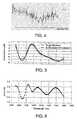
- FIG. 4is a plot of transmission over time relating transitions in the interference effects of the monitoring beam with turning points in the deposition of a succession of unit sub-layers.
- FIG. 5is a pair of plots contrasting a simulated spectral response of our filter Example A with a target spectral response.
- FIG. 6plots the contrast of FIG. 5 .
- FIG. 7is a schematic cross-sectional view of another version of our gain-flattening interference filter assembled by levels.
- FIG. 8is a cross-sectional view of high and low index sub-layers organized into a set of base permutations from which each of the levels of the alternative filter can be filled.
- FIG. 9is a pair of plots contrasting a simulated spectral response of our filter Example B with a target spectral response.
- FIG. 10plots the contrast of FIG. 9 .
- FIG. 1An exemplary gain-flattening thin-film interference filter 10 arranged in accordance with our invention is depicted in FIG. 1 .
- the interference filter 10is mounted within an optical coupler 30 between input and output fiber sections 26 and 28 of a fiber optic communications system.
- a light beam 24 conveying a plurality of different wavelength channelsdiverges from the input fiber section 26 and is collimated by a lens 32 for passing through the interference filter 10 as substantially parallel light.
- Another lens 34collects the parallel light emerging from the interference filter 10 and converges the light through a focus on the output fiber section 28 .
- the interference filter 10can be mounted in a variety of other optical coupling arrangements common to the art for conveying a plurality of different wavelength channels through the filter 10 .
- the interference filter 10is placed after or between stages of an amplifier (not shown) such as an erbium-doped fiber amplifier.
- an amplifiernot shown
- the highest gain wavelength channelsare attenuated most so that all of the channels experience approximately the same net gain.
- the exemplary gain-flattening interference filter 10is constructed by a series of layers 14 and 16 having different refractive indices supported on a common substrate 12 .
- the substrate 12can be made from a variety of glasses and other materials including Schott BK7, Schott F7, Schott DWDM-20 or DWDM-22 (Schott Glass Technologies, Duryea, Pa.) Hoya WDM-100 (Hoya Corporation, Lewisville Tex.), and Ohara WMS-13 (Ohara Corporation, Branchburg, N.J.).
- the so-called “high” index layers 14can be made of a transmissive material such as Ta 2 O 5 .
- the so-called “low” index layers 16can be made of a transmissive material such as SiO 2 .
- Both metal oxidesare preferably vacuum deposited onto the substrate 12 using energetic plasma-based techniques, such as ion beam or magnetron sputtering and reactive ion plating, within an evacuated environment.
- Other metal oxides having appropriate qualities for forming the layers 14 or 16include Nb 2 O 5 , TiO 2 , ZrO 2 , and Al 2 O 3 .
- each of the high and low index layers 14 and 16also differ in physical thickness to support a more complex spectral response.
- the thickness variationsare limited to integer multiples of quarter-wavelength travels of a monitoring light beam 20 as transmitted through the layers 14 and 16 .
- FIG. 3shows an exemplary low index layer 16 composed of three sub-layers 16 ′, each having a thickness equal to a quarter wavelength travel of the monitoring light beam 20 as transmitted through the sub-layers 16 ′.
- the monitoring beam 20 as also seen in FIG. 2is preferably a narrow-band (i.e., temporally coherent) light beam emitted by a laser 18 and is monitored by a intensity sensor 22 for measuring variations in the transmission efficiency of the filter 10 as the layers 14 and 16 are deposited.
- a similar intensity sensor 22could be used for monitoring reflections from the filter 10 , which can increase the contrast of the extrema for layers that are insensitive in transmission.
- our assembly of our gain-flattening interference filter 10 from sub-layers having unit thicknesses equal to a quarter wavelength travel of the monitoring beam 20enables our interference filter (a) to exhibit the complex spectral responses required of gain-flattening filters and (b) to be produced by so-called “turning point monitoring” techniques previously limited to less complex spectral responses.
- the use of “turning point monitoring” techniquesprovides for producing our gain-flattening interference filter 10 with the higher manufacturing accuracy previously reserved for simpler interference filter designs.
- FIG. 4A typical transmission versus time plot for the monitoring beam 20 during a vacuum deposition process (e.g., sputtering) of the two different index materials is shown in FIG. 4 .
- An oscillating pattern of transmission variationoccurs during the deposition process.
- Turning points associated with the demarcated troughs and peaksindicate local variations between constructive and destructive interference. For example, the troughs indicate a local extreme of destructive interference, and the peaks indicate a local extreme of constructive interference.
- the extremes of constructive and destructive interferenceoccur during the deposition process at layer thicknesses corresponding to a multiple of the quarter wavelength travel of the monitoring beam 20 as transmitted through the layers 14 and 16 .
- the transmission extrema of the monitoring beam 20are used as turning points for switching deposition from one of the high and low index layers 14 and 16 to the other of the high and low index layers 14 and 16 .
- Each transition from peak to trough or trough to peakrepresents a quarter-wavelength deposition thickness.
- the selected turning pointscan occur after a single transition or after multiple transitions for depositing layers 14 or 16 having thicknesses equal to a multiple of the quarter-wavelength travel of the monitoring beam 20 .
- the monitoring beam 20is transmitted through a single spot (as shown) or through multiple spots on the substrate 12 , which during deposition can be in the form of a 30 centimeter (cm) diameter disk. Spots about a particular radius of the disk can be averaged to monitor deposition consistency over a larger area of the substrate 12 .
- Freedoms available for matching the desired spectral response with our gain-flattening filterinclude variations in the total number of layers 14 and 16 , in the refractive indices of the layers 14 and 16 , and in the wavelength of the monitoring beam 20 .
- the number of unit sub-layersis preferably limited to between 80 and 200 sub-layers.
- the refractive indicesare limited by available choices of optical materials that are transmissive within the wavelength range of the different wavelength channels.
- the monitoring wavelengthis also limited by the transmission spectra of the layer materials. However, we have found that preferred wavelengths of the monitoring beam 20 are generally beyond the working range of wavelengths intended for attenuation by the filter 10 . Longer wavelengths (e.g., 10 nm to 100 nm larger than the central wavelength of the filter) produce some of the best designs.
- Various algorithmscan be used for optimizing these starting variables within the bounds of physical practicalities such as substituting procedures that compare proposed designs with a merit function.
- a design having given number of layers with thicknesses limited to a multiple of a given monitoring beam's quarter wavelength in the layer materialscan be modeled by conventional optical principles to yield a simulated spectral response.
- a merit functionsuch as a normalized sum of the squares (at a set of discrete wavelengths) of the differences between the target and simulated responses, can be used to compare the simulated spectral response to the desired spectral response and note the difference.
- FIG. 6plots a measured difference between the simulated and desired spectral responses plotted in FIG. 5 .
- Design comparisonscan be made by flipping each layer one at a time from a high index layer 14 to a low index layer 16 or from a low index layer 16 to a high index layer 14 and by maintaining any change that better satisfies the merit function.
- the iterationscan step from one end of the stack of layers 14 and 16 to the other or from some point in the middle of the stack of layers 14 and 16 to both ends and can be repeated (typically five or six times) until the changes do not provide any significant further improvement.
- the best interim designis stored.
- a variablesuch as the number of layers or the monitoring wavelength is then changed, and further iterations are conducted until another best interim design is determined for the new combination of starting variables.
- the stored best interim designsare compared with each other, but not necessarily in accordance with the original merit function alone.
- the best interim designscan be compared based on design stability and manufactureability. Designs that (a) are less sensitive to manufacturing errors, (b) have the fewest number of layers, and (c) use monitoring wavelengths that maximize signal-to-noise ratio are preferred. For example, designs that exhibit the largest second order derivatives at the extrema in the transmission vs. time plot enable turning points to be identified more precisely during the deposition process.
- combinations of layers that produce so-called “insensitive” layersare preferably avoided.
- Glass substrates, such as the substrate 12can have refractive indices similar to one of the high and low index layers 14 or 16 . If the first layer or any combination of layers equivalent to a first layer has inadequate refractive index contrast with the substrate 12 , interference extrema associated with the deposit of the insensitive layer are significantly weakened.
- Equivalent combinations of layers that are avoidedinclude balanced pairs of high and low index layers, producing all half-wavelength multiples between a layer under deposit (i.e., the equivalent first layer) and the substrate 12 .
- the intensity of the monitoring beam 20can be measured in reflection from the filter 10 to enhance contrast between the weaker extrema (as a percentage difference of the reflected beam) of otherwise insensitive layers.
- the filter 10can be composed of layers exhibiting three or more different refractive indices.
- the high and low refractive index layerscan be mixed within the quarter-wavelength unit sub-layers to provide mid-index sub-layers.
- the additional refractive index sub-layersfurther expand options for arriving at a best design.
- the processing time for determining the simulated spectral response for each iterationcan be significant and limit the number of iterations that can be carried out in an allotted time.
- Our inventionin a preferred embodiment simplifies the determination of individual spectral responses by (a) organizing combinations of the high, low, or other different index sub-layers 14 ′ and 16 ′ into a set of base permutations including alternatives that vary in both number and order of the different index sub-layers 14 ′ and 16 ′, (b) assembling the high, low, or other different index layers 14 and 16 into a plurality of levels, and (c) filling each of the levels with one of the alternatives from the set of base permutations. Time is saved by pre-calculating the contribution of each permutation to the overall spectral response.
- FIG. 7depicts a gain-flattening filter 40 assembled by levels 42 a - 42 e on a common substrate 44 .
- FIG. 8depicts a set 50 of base permutations labeled H, L, HH, HL, LH, LL, HHH, HHL, HLH, LHH, HLL, LHL, LLH, and LLL for delineating alternative combinations of the high (H) and low (L) index sub-layers 14 ′ and 16 ′ that vary in both number and order.
- the depicted set 50 of base permutationsvaries in number of combined sub-levels from one to three and includes every possible order of the sub-layers 14 ′ and 16 ′ within each allotted number of combined sub-levels.
- Each of the levels 42 a - 42 e of the filter 40is filled by one of the alternative permutations H, L, HH, HL, LH, LL, HHH, HHL, HLH, LHH, HLL, LHL, LLH, and LLL from the set 50 of base permutations.
- the level 42 ais filled by the permutation HLH
- the level 42 bis filled by the permutation LL
- the level 42 cis filled by the permutation HHL
- the level 42 dis filled by the permutation L
- the level 42 eis filled by the permutation LHH.
- the spectral filtering contribution of each of the permutations H, L, HH, HL, LH, LL, HHH, HHL, HLH, LHH, HLL, LHL, LLH, and LLL from the set 50 of base permutationsis pre-calculated to reduce processing time.
- the entire set 50 of base permutationscan be substituted one at a time for each level 42 a - 42 e , and the optical performance characteristics of the resulting filter 40 can be compared to the desired filter spectral response (e.g., the determined relative optical power adjustments among the plurality of different wavelength channels) according to a prescribed merit function.
- the base permutation H, L, HH, HL, LH, LL, HHH, HHL, HLH, LHH, HLL, LHL, LLH, or LLL that best satisfies the merit function among its set of peers in each one of the levels 42 a - 42 eis maintained during a similar round of substitutions for each other of the levels 42 a - 42 e .
- the levels 42 a - 42 ecan be assessed in various orders, and the same or a different order of assessment can be repeated until no further significant improvement is achieved.
- the exemplary gain-flattening interference filters 10 and 40are illustrated with just a limited number of layers 14 and 16 , tens to hundreds of the layers are generally required for achieving many of the desired complex spectral responses. Further variation in spectral response can be achieved by constructing unit sub-layers from three or more refractive index materials. The third material greatly expands the number of unit sub-layer permutations available for substitution.
- the high and low refractive index materialscan be combined within the same unit sub-layer to construct a mid-refractive index sub-layer.
- the concept of the Herpin Equivalent Indexcan be used to replace a layer of homogeneous material having a particular refractive index with an equivalent structure containing a symmetric arrangement of layers of different materials having two different refractive indices.
- the division of high and low refractive index materials within the same unit sub-layercannot be regulated by “turning point monitoring” techniques, the technique can be used to regulate the thickness of the mid-index sub-layer itself.
- Our thin-film interference filtersare preferably constructed with all quarter-wavelength unit sub-layers for achieving most spectral responses.
- one or more non-quarter-wavelength based layerscan be added at the end of the deposition process to increase design flexibility or to perform additional functions.
- non-quarter-wavelength based layerscan be added to the end of an otherwise all-quarter wavelength based filter to further refine the filter's spectral response.
- An example of our new gain-flattening interference filter arranged for matching the target spectrum of FIG. 5is constructed with a succession of high (H) and low (L) index unit sub-layers according to the following pattern:
- Airrefers to the medium above the filter
- Substraterefers to the glass substrate upon which the sub-layers are deposited.
- the high (H) and low (L) index sub-layers listed abovehave thicknesses equal to a single quarter wavelength of a 1629.5 nanometer (nm) wavelength monitoring beam as transmitted through the sub-layers.
- the high-index (H) sub-layersare made of Nb 2 O 5 and have a refractive index of 2.1341 at the monitoring beam wavelength.
- the low-index (L) sub-layersare made of SiO 2 and have a refractive index of 1.4490 at the monitoring beam wavelength.
- the refractive indices of the deposited layersare sensitive to the energetics of the selected deposition process (e.g., evaporation or ion beam sputtering), which should be considered in matching the simulated designs to actual designs.
- the high (H) and low (L) index sub-layersshare the same optical thickness (however far the monitoring beam happens to travel through one-quarter wavelength) but differ from each other in physical thickness as an inverse ratio of their refractive indices.
- the precise thicknesses of the high (H) and low (L) index sub-layersare equal to one-quarter of the monitoring beam wavelength (in a vacuum) divided by the refractive indices of the sub-layers.
- the quarter-wavelength thicknessesare based on the somewhat different wavelengths of the monitoring beam while propagating through the high and low index materials.
- a total of 186 sub-layersare employed at a combined thickness of 43.64 microns ( ⁇ m).
- the central wavelength of the target spectral responseis noted to be around 1550 nanometers (nm) and covers an approximate working range from 1528 nm to 1560 nm.
- the 1629.5 nm wavelength of the monitoring beamis well beyond and above this range.
- the high (H) and low (L) index sub-layers listed abovehave thicknesses equal to a single quarter wavelength of a 1584 nanometer (nm) wavelength monitoring beam as transmitted through the sub-layers.
- the substratewhich is made of glass, has a refractive index of 1.579.
- the high-index (H) sub-layersare made of Ta 2 O 5 and have a refractive index of 2.0717 at the monitoring beam wavelength.
- the low-index (L) sub-layersare made of SiO 2 and have a refractive index of 1.4748 at the monitoring beam wavelength.
- a total of 158 sub-layersare employed at a combined thickness of 36.08 microns ( ⁇ m).
- the simulated response (designed spectrum) of the exemplary filterclosely matches the target response (target spectrum) within a peak-to-peak error function of 0.93 decibels (dB). This match was achieved over a working range between 1528 nm 1566 nm with combinations of high (H) and low (L) index sub layers that do not depart from quarter wavelength optical thickness.
- An example of our new method of designing a thin-film interference filter for gain flatteningincludes the following steps:
- the materialsshould be low-loss (transmissive) materials that significantly differ in refractive index.
- a monitoring beam wavelength range between 1560 nm and 1640 nmis typically appropriate for a filter with a central wavelength of 1550 nm.
- each of the levelsperform a series of substitutions: (a) cycling through each of the base permutations, (b) calculating a new simulated spectral response for each new filter design based on the saved permutation transfer matrices, (c) comparing the simulated response with the target response, and (d) refilling the level with the base permutation that best satisfies a merit function.
Landscapes
- Physics & Mathematics (AREA)
- General Physics & Mathematics (AREA)
- Optics & Photonics (AREA)
- Optical Filters (AREA)
Abstract
Description
Claims (46)
Priority Applications (1)
| Application Number | Priority Date | Filing Date | Title |
|---|---|---|---|
| US10/028,031US6611378B1 (en) | 2001-12-20 | 2001-12-20 | Thin-film interference filter with quarter-wavelength unit sub-layers arranged in a generalized pattern |
Applications Claiming Priority (1)
| Application Number | Priority Date | Filing Date | Title |
|---|---|---|---|
| US10/028,031US6611378B1 (en) | 2001-12-20 | 2001-12-20 | Thin-film interference filter with quarter-wavelength unit sub-layers arranged in a generalized pattern |
Publications (1)
| Publication Number | Publication Date |
|---|---|
| US6611378B1true US6611378B1 (en) | 2003-08-26 |
Family
ID=27752575
Family Applications (1)
| Application Number | Title | Priority Date | Filing Date |
|---|---|---|---|
| US10/028,031Expired - LifetimeUS6611378B1 (en) | 2001-12-20 | 2001-12-20 | Thin-film interference filter with quarter-wavelength unit sub-layers arranged in a generalized pattern |
Country Status (1)
| Country | Link |
|---|---|
| US (1) | US6611378B1 (en) |
Cited By (27)
| Publication number | Priority date | Publication date | Assignee | Title |
|---|---|---|---|---|
| US20020154387A1 (en)* | 2001-04-20 | 2002-10-24 | Kenji Mori | Gain equalizer, collimator with gain equalizer and method of manufacturing gain equalizer |
| US20030179997A1 (en)* | 2002-03-21 | 2003-09-25 | Hwang Seong-Taek | Gain flattening filter and gain flattened optical fiber amplifier employing the same |
| EP1524535A1 (en)* | 2003-10-14 | 2005-04-20 | Olympus Corporation | Optical multi-layer filter with periodical variation of the high and low refractive index and optical instrument |
| US20050220154A1 (en)* | 2004-03-24 | 2005-10-06 | National Institute Of Advanced Industrial Science And Technology | Broadband mode-locked laser oscillator and oscillation method thereof |
| US20060092516A1 (en)* | 2003-06-26 | 2006-05-04 | Nikon Corporation | Method for producing multilayer optical device |
| US20060198025A1 (en)* | 2005-03-04 | 2006-09-07 | Ga-Lane Chen | Optical filter |
| US20070002432A1 (en)* | 2005-07-01 | 2007-01-04 | Hon Hai Precision Industry Co., Ltd. | Optical filter for screening out infrared and ultraviolet light |
| US20070002433A1 (en)* | 2005-07-01 | 2007-01-04 | Hon Hai Precision Industry Co., Ltd. | Optical filter for screening out infrared and ultraviolet light |
| EP1753101A1 (en)* | 2005-08-08 | 2007-02-14 | The Regents of the University of Colorado | Gain flattening filter for preserving the spectral bandwidth in cryogenic ultrashort-pulse laser amplifiers |
| US20070082418A1 (en)* | 2005-10-11 | 2007-04-12 | National Chung-Hsing University | Method for manufacturing a light emitting device and light emitting device made therefrom |
| US7228025B1 (en)* | 2002-10-31 | 2007-06-05 | Finisar Corporation | Thin film interleaver |
| US20070223008A1 (en)* | 2002-01-04 | 2007-09-27 | Takahiro Itoh | Wavelength determining apparatus, method and program for thin film thickness monitoring light |
| US20070228527A1 (en)* | 2005-05-10 | 2007-10-04 | Tokyo Electron Limited | Substrate for electronic device and method for processing same |
| US20080037129A1 (en)* | 2006-05-12 | 2008-02-14 | Semrock, Inc. | Multiphoton fluorescence filters |
| CN100373186C (en)* | 2004-10-19 | 2008-03-05 | 同济大学 | One-pass-band two-channel filter with independent adjustment of channel pass-band relative position |
| CN100373185C (en)* | 2004-10-11 | 2008-03-05 | 同济大学 | Channel passband filters with independently adjustable relative positions |
| CN100386655C (en)* | 2005-10-27 | 2008-05-07 | 亚洲光学股份有限公司 | Three-channel optical filter |
| CN100430757C (en)* | 2005-12-08 | 2008-11-05 | 亚洲光学股份有限公司 | Bandpass filter capable of reducing coating layer number |
| CN100454050C (en)* | 2005-07-15 | 2009-01-21 | 鸿富锦精密工业(深圳)有限公司 | filter device |
| CN100462738C (en)* | 2005-07-15 | 2009-02-18 | 鸿富锦精密工业(深圳)有限公司 | filter device |
| US20090122408A1 (en)* | 2007-11-09 | 2009-05-14 | Hon Hai Precision Industry Co., Ltd. | Dichroic mirror |
| US20090141358A1 (en)* | 2007-11-30 | 2009-06-04 | Cangemi Michael J | Dense homogeneous fluoride films for duv elements and method of preparing same |
| US20110170164A1 (en)* | 2010-01-08 | 2011-07-14 | Ligang Wang | Tunable thin-film filter |
| US8879150B1 (en) | 2009-03-20 | 2014-11-04 | Semrock, Inc. | Optical thin-film polarizing bandpass filter |
| US8958156B1 (en) | 2007-05-30 | 2015-02-17 | Semrock, Inc. | Interference filter for non-zero angle of incidence spectroscopy |
| US9304237B1 (en) | 2012-12-10 | 2016-04-05 | Semrock, Inc. | Tunable band-pass filter |
| US9354370B1 (en) | 2007-09-25 | 2016-05-31 | Semrock, Inc. | Optical thin-film notch filter with very wide pass band regions |
Citations (44)
| Publication number | Priority date | Publication date | Assignee | Title |
|---|---|---|---|---|
| US3551017A (en) | 1967-05-19 | 1970-12-29 | Hitachi Ltd | Far infrared transmission type interference filter |
| US3697153A (en) | 1969-12-17 | 1972-10-10 | Balzers Patent Beteilig Ag | Multilayer optical interference filter with wideband spectral transmission region and reduced ripple |
| US3759604A (en)* | 1970-09-18 | 1973-09-18 | Balzers Patent Beteilig Ag | Interference filter reflecting a certain wave length band within a given wave length range while letting pass other wave length bands of the range |
| US3914023A (en) | 1972-12-08 | 1975-10-21 | Balzers Patent Beteilig Ag | Wide-band multilayer interference filter |
| US4009453A (en) | 1974-10-16 | 1977-02-22 | Siemens Aktiengesellschaft | Narrow-band interference filter and its application in a laser system |
| US4229066A (en)* | 1978-09-20 | 1980-10-21 | Optical Coating Laboratory, Inc. | Visible transmitting and infrared reflecting filter |
| US4531838A (en) | 1981-03-26 | 1985-07-30 | Canon Kabushiki Kaisha | Method and device for controlling the film thickness of evaporated film |
| US4582431A (en) | 1983-10-11 | 1986-04-15 | Honeywell Inc. | Optical monitor for direct thickness control of transparent films |
| US4663557A (en)* | 1981-07-20 | 1987-05-05 | Optical Coating Laboratory, Inc. | Optical coatings for high temperature applications |
| US4666250A (en) | 1985-04-16 | 1987-05-19 | Rockwell International Corporation | Interference filter design using flip-flop optimization |
| US4747666A (en) | 1985-06-25 | 1988-05-31 | Horiba, Ltd. | Multi-layer interference filter |
| US4778251A (en) | 1987-03-09 | 1988-10-18 | Rockwell International Corporation | Thickness error compensation for digital gradient-index optical coatings |
| US4793669A (en) | 1987-09-11 | 1988-12-27 | Coherent, Inc. | Multilayer optical filter for producing colored reflected light and neutral transmission |
| US4832448A (en) | 1986-10-10 | 1989-05-23 | Pilkington P.E. Limited | Interference filter |
| US4909631A (en) | 1987-12-18 | 1990-03-20 | Tan Raul Y | Method for film thickness and refractive index determination |
| US5035485A (en) | 1988-12-23 | 1991-07-30 | Minolta Camera Kabushiki Kaisha | Interference filter with sharp cutoff characteristics |
| US5138222A (en) | 1989-06-27 | 1992-08-11 | Mitsubishi Denki Kabushiki Kaisha | Projection cathode ray tube having an interference filter |
| US5179468A (en) | 1991-11-05 | 1993-01-12 | Gte Products Corporation | Interleaving of similar thin-film stacks for producing optical interference coatings |
| US5181143A (en) | 1991-10-03 | 1993-01-19 | Rockwell International Corporation | Multiple line rugate filter with index clipping |
| US5233464A (en) | 1991-03-20 | 1993-08-03 | Costich Verne R | Multilayer infrared filter |
| US5241417A (en) | 1990-02-09 | 1993-08-31 | Copal Company Limited | Multi-layered optical filter film and production method thereof |
| US5245474A (en) | 1988-03-22 | 1993-09-14 | Compagnie Generale D'electricite | Electromagnetic filter device |
| US5274661A (en) | 1992-12-07 | 1993-12-28 | Spectra Physics Lasers, Inc. | Thin film dielectric coating for laser resonator |
| US5355217A (en) | 1991-08-14 | 1994-10-11 | Sofie | Assembly for simultaneous observation and laser interferometric measurements, in particular on thin-film structures |
| US5410431A (en) | 1993-06-01 | 1995-04-25 | Rockwell International Corporation | Multi-line narrowband-pass filters |
| US5425964A (en)* | 1994-07-22 | 1995-06-20 | Rockwell International Corporation | Deposition of multiple layer thin films using a broadband spectral monitor |
| US5625492A (en) | 1992-09-18 | 1997-04-29 | Leica Mikroskopie Und Systeme Gmbh | Color compensation filter |
| US5719989A (en) | 1995-06-28 | 1998-02-17 | Jds Fitel Inc. | Multilayer thin film bandpass filter |
| US5889592A (en) | 1998-03-18 | 1999-03-30 | Zawaideh; Emad | Nondestructive optical techniques for simultaneously measuring optical constants and thicknesses of single and multilayer films |
| US5923429A (en) | 1998-03-05 | 1999-07-13 | International Business Machines Corporation | Apparatus for monitoring in-situ the thickness of a film during film deposition and a method thereof |
| US5926317A (en) | 1996-11-06 | 1999-07-20 | Jds Fitel Inc. | Multilayer thin film dielectric bandpass filter |
| US5999322A (en) | 1995-06-28 | 1999-12-07 | Cushing; David Henry | Multilayer thin film bandpass filter |
| US5999267A (en) | 1999-03-08 | 1999-12-07 | Zawaideh; Emad | Nondestructive optical techniques for simultaneously measuring optical constants and thicknesses of single and multilayer films |
| US6011652A (en) | 1997-12-23 | 2000-01-04 | Cushing; David Henry | Multilayer thin film dielectric bandpass filter |
| US6034772A (en) | 1998-10-29 | 2000-03-07 | Eastman Kodak Company | Method for processing interferometric measurement data |
| US6046854A (en) | 1996-02-09 | 2000-04-04 | Corning Incorporated | Multi-path interference filter with reflective surfaces |
| US6115180A (en) | 1998-06-22 | 2000-09-05 | Alps Electric Co., Ltd. | Optical multilayered-film filter |
| US6117530A (en) | 1993-12-21 | 2000-09-12 | 3M Innovative Properties Company | Optical film |
| US6137575A (en) | 1997-10-24 | 2000-10-24 | Canon Kabushiki Kaisha | Film thickness measuring method and apparatus |
| US6157490A (en) | 1998-01-13 | 2000-12-05 | 3M Innovative Properties Company | Optical film with sharpened bandedge |
| US6208466B1 (en) | 1998-11-25 | 2001-03-27 | 3M Innovative Properties Company | Multilayer reflector with selective transmission |
| US6432471B1 (en)* | 1998-11-09 | 2002-08-13 | Massachusetts Institute Of Technology | Method for generating an anti-reflection coating for a laser diode |
| US20020131176A1 (en)* | 2001-01-26 | 2002-09-19 | Ciena Corporation | Multi-channel optical filter |
| US6481369B1 (en)* | 1999-10-14 | 2002-11-19 | Hoya Corporation | Thin film forming method and apparatus |
- 2001
- 2001-12-20USUS10/028,031patent/US6611378B1/ennot_activeExpired - Lifetime
Patent Citations (45)
| Publication number | Priority date | Publication date | Assignee | Title |
|---|---|---|---|---|
| US3551017A (en) | 1967-05-19 | 1970-12-29 | Hitachi Ltd | Far infrared transmission type interference filter |
| US3697153A (en) | 1969-12-17 | 1972-10-10 | Balzers Patent Beteilig Ag | Multilayer optical interference filter with wideband spectral transmission region and reduced ripple |
| US3759604A (en)* | 1970-09-18 | 1973-09-18 | Balzers Patent Beteilig Ag | Interference filter reflecting a certain wave length band within a given wave length range while letting pass other wave length bands of the range |
| US3914023A (en) | 1972-12-08 | 1975-10-21 | Balzers Patent Beteilig Ag | Wide-band multilayer interference filter |
| US4009453A (en) | 1974-10-16 | 1977-02-22 | Siemens Aktiengesellschaft | Narrow-band interference filter and its application in a laser system |
| US4229066A (en)* | 1978-09-20 | 1980-10-21 | Optical Coating Laboratory, Inc. | Visible transmitting and infrared reflecting filter |
| US4531838A (en) | 1981-03-26 | 1985-07-30 | Canon Kabushiki Kaisha | Method and device for controlling the film thickness of evaporated film |
| US4663557A (en)* | 1981-07-20 | 1987-05-05 | Optical Coating Laboratory, Inc. | Optical coatings for high temperature applications |
| US4582431A (en) | 1983-10-11 | 1986-04-15 | Honeywell Inc. | Optical monitor for direct thickness control of transparent films |
| US4666250A (en) | 1985-04-16 | 1987-05-19 | Rockwell International Corporation | Interference filter design using flip-flop optimization |
| US4747666A (en) | 1985-06-25 | 1988-05-31 | Horiba, Ltd. | Multi-layer interference filter |
| US4832448A (en) | 1986-10-10 | 1989-05-23 | Pilkington P.E. Limited | Interference filter |
| US4778251A (en) | 1987-03-09 | 1988-10-18 | Rockwell International Corporation | Thickness error compensation for digital gradient-index optical coatings |
| US4793669A (en) | 1987-09-11 | 1988-12-27 | Coherent, Inc. | Multilayer optical filter for producing colored reflected light and neutral transmission |
| US4909631A (en) | 1987-12-18 | 1990-03-20 | Tan Raul Y | Method for film thickness and refractive index determination |
| US5245474A (en) | 1988-03-22 | 1993-09-14 | Compagnie Generale D'electricite | Electromagnetic filter device |
| US5035485A (en) | 1988-12-23 | 1991-07-30 | Minolta Camera Kabushiki Kaisha | Interference filter with sharp cutoff characteristics |
| US5138222A (en) | 1989-06-27 | 1992-08-11 | Mitsubishi Denki Kabushiki Kaisha | Projection cathode ray tube having an interference filter |
| US5241417A (en) | 1990-02-09 | 1993-08-31 | Copal Company Limited | Multi-layered optical filter film and production method thereof |
| US5233464A (en) | 1991-03-20 | 1993-08-03 | Costich Verne R | Multilayer infrared filter |
| US5426532A (en) | 1991-03-20 | 1995-06-20 | Costich; Verne R. | Infrared filter |
| US5355217A (en) | 1991-08-14 | 1994-10-11 | Sofie | Assembly for simultaneous observation and laser interferometric measurements, in particular on thin-film structures |
| US5181143A (en) | 1991-10-03 | 1993-01-19 | Rockwell International Corporation | Multiple line rugate filter with index clipping |
| US5179468A (en) | 1991-11-05 | 1993-01-12 | Gte Products Corporation | Interleaving of similar thin-film stacks for producing optical interference coatings |
| US5625492A (en) | 1992-09-18 | 1997-04-29 | Leica Mikroskopie Und Systeme Gmbh | Color compensation filter |
| US5274661A (en) | 1992-12-07 | 1993-12-28 | Spectra Physics Lasers, Inc. | Thin film dielectric coating for laser resonator |
| US5410431A (en) | 1993-06-01 | 1995-04-25 | Rockwell International Corporation | Multi-line narrowband-pass filters |
| US6117530A (en) | 1993-12-21 | 2000-09-12 | 3M Innovative Properties Company | Optical film |
| US5425964A (en)* | 1994-07-22 | 1995-06-20 | Rockwell International Corporation | Deposition of multiple layer thin films using a broadband spectral monitor |
| US5719989A (en) | 1995-06-28 | 1998-02-17 | Jds Fitel Inc. | Multilayer thin film bandpass filter |
| US5999322A (en) | 1995-06-28 | 1999-12-07 | Cushing; David Henry | Multilayer thin film bandpass filter |
| US6046854A (en) | 1996-02-09 | 2000-04-04 | Corning Incorporated | Multi-path interference filter with reflective surfaces |
| US5926317A (en) | 1996-11-06 | 1999-07-20 | Jds Fitel Inc. | Multilayer thin film dielectric bandpass filter |
| US6137575A (en) | 1997-10-24 | 2000-10-24 | Canon Kabushiki Kaisha | Film thickness measuring method and apparatus |
| US6011652A (en) | 1997-12-23 | 2000-01-04 | Cushing; David Henry | Multilayer thin film dielectric bandpass filter |
| US6157490A (en) | 1998-01-13 | 2000-12-05 | 3M Innovative Properties Company | Optical film with sharpened bandedge |
| US5923429A (en) | 1998-03-05 | 1999-07-13 | International Business Machines Corporation | Apparatus for monitoring in-situ the thickness of a film during film deposition and a method thereof |
| US5889592A (en) | 1998-03-18 | 1999-03-30 | Zawaideh; Emad | Nondestructive optical techniques for simultaneously measuring optical constants and thicknesses of single and multilayer films |
| US6115180A (en) | 1998-06-22 | 2000-09-05 | Alps Electric Co., Ltd. | Optical multilayered-film filter |
| US6034772A (en) | 1998-10-29 | 2000-03-07 | Eastman Kodak Company | Method for processing interferometric measurement data |
| US6432471B1 (en)* | 1998-11-09 | 2002-08-13 | Massachusetts Institute Of Technology | Method for generating an anti-reflection coating for a laser diode |
| US6208466B1 (en) | 1998-11-25 | 2001-03-27 | 3M Innovative Properties Company | Multilayer reflector with selective transmission |
| US5999267A (en) | 1999-03-08 | 1999-12-07 | Zawaideh; Emad | Nondestructive optical techniques for simultaneously measuring optical constants and thicknesses of single and multilayer films |
| US6481369B1 (en)* | 1999-10-14 | 2002-11-19 | Hoya Corporation | Thin film forming method and apparatus |
| US20020131176A1 (en)* | 2001-01-26 | 2002-09-19 | Ciena Corporation | Multi-channel optical filter |
Non-Patent Citations (9)
| Title |
|---|
| "Coating design using very thin high- and low-index layers", W.H. Southwell, Applied Optics, vol. 14, No. 4, Feb. 15, 1985, pp. 457-460. |
| "Completely Automatic Synthesis of Optical Thin Film Systems", J.A, Dobrowolski, P. H. Berning, Applied Optics, vol. 4, No. 8, Aug. 1995, pp. 937-946. |
| "Flip-flop thin-film design program with enhanced capabilities", J.A, Dobrowolski and R.A. Kemp, Applied Optics, vol. 31, No. 19, Jul. 1, 1992, pp. 3807-3812. |
| "Gradient-index antireflection coatings", W.H. Southwell, Optics Letters, vol. 8, No. 11, Nov. 1983, pp. 584-586. |
| "Optical Behaviour Of Gradient-Index Multilayer Films", V.N. Yadava, S.K. Sharma, and K.L. Chopra, Thin Solid Films 21, 1974, pp. 297-312. |
| "The Design of Optical Filers", L.I. Epstein, Journal of the Optical Society of American, vol. 42, No. 11, Nov. 1952, pp. 806-810. |
| "Thin Films II, Contributed Papers", A. J. Thelen, 1982 Annual Meeting Optical Society of America, Tuesday, Oct. 19, 1982, pp. 1732. |
| "Turning point monitoring of narrow-band all-dielectric thin-film optical fiters", H.A. Macleod, Optical Acta., vol. 19, No. 1, 1972, pp. 1-28. |
| "Use of Equivalent Films in the Design of Infrared Multilayer Antireflection Coatings", Journal of the Optical Society of America, vol. 52, No. 4, Apr. 1962, pp. 431-436. |
Cited By (46)
| Publication number | Priority date | Publication date | Assignee | Title |
|---|---|---|---|---|
| US20020154387A1 (en)* | 2001-04-20 | 2002-10-24 | Kenji Mori | Gain equalizer, collimator with gain equalizer and method of manufacturing gain equalizer |
| US20070223008A1 (en)* | 2002-01-04 | 2007-09-27 | Takahiro Itoh | Wavelength determining apparatus, method and program for thin film thickness monitoring light |
| US20100284062A1 (en)* | 2002-01-04 | 2010-11-11 | The Furukawa Electric Co., Ltd. | Wavelength determining apparatus, method and program for thin film thickness monitoring light |
| US8174757B2 (en)* | 2002-01-04 | 2012-05-08 | The Furukawa Electric Co., Ltd. | Wavelength determining apparatus, method and program for thin film thickness monitoring light |
| US20030179997A1 (en)* | 2002-03-21 | 2003-09-25 | Hwang Seong-Taek | Gain flattening filter and gain flattened optical fiber amplifier employing the same |
| US7104700B2 (en)* | 2002-03-21 | 2006-09-12 | Samsung Electronics, Co., Ltd. | Gain flattening filter and gain flattened optical fiber amplifier employing the same |
| US7228025B1 (en)* | 2002-10-31 | 2007-06-05 | Finisar Corporation | Thin film interleaver |
| US7544392B2 (en)* | 2003-06-26 | 2009-06-09 | Nikon Corporation | Method for producing multilayer optical device |
| US20060092516A1 (en)* | 2003-06-26 | 2006-05-04 | Nikon Corporation | Method for producing multilayer optical device |
| US20070196586A1 (en)* | 2003-06-26 | 2007-08-23 | Nikon Corporation | Method for producing multilayer optical device |
| US7130125B2 (en) | 2003-10-14 | 2006-10-31 | Olympus Corporation | Optical filter and optical device |
| EP1524535A1 (en)* | 2003-10-14 | 2005-04-20 | Olympus Corporation | Optical multi-layer filter with periodical variation of the high and low refractive index and optical instrument |
| US20050111103A1 (en)* | 2003-10-14 | 2005-05-26 | Yoshiki Shinta | Optical filter and optical device |
| CN1333272C (en)* | 2003-10-14 | 2007-08-22 | 奥林巴斯株式会社 | Optical filter and optical instrument |
| US20050220154A1 (en)* | 2004-03-24 | 2005-10-06 | National Institute Of Advanced Industrial Science And Technology | Broadband mode-locked laser oscillator and oscillation method thereof |
| US7776736B2 (en)* | 2004-05-11 | 2010-08-17 | Tokyo Electron Limited | Substrate for electronic device capable of suppressing fluorine atoms exposed at the surface of insulating film from reacting with water and method for processing same |
| CN100373185C (en)* | 2004-10-11 | 2008-03-05 | 同济大学 | Channel passband filters with independently adjustable relative positions |
| CN100373186C (en)* | 2004-10-19 | 2008-03-05 | 同济大学 | One-pass-band two-channel filter with independent adjustment of channel pass-band relative position |
| US7450306B2 (en)* | 2005-03-04 | 2008-11-11 | Hon Hai Precision Industry Co., Ltd. | Optical filter for blocking UV light and IR light |
| US20060198025A1 (en)* | 2005-03-04 | 2006-09-07 | Ga-Lane Chen | Optical filter |
| US20070228527A1 (en)* | 2005-05-10 | 2007-10-04 | Tokyo Electron Limited | Substrate for electronic device and method for processing same |
| US7212336B2 (en)* | 2005-07-01 | 2007-05-01 | Hon Hai Precision Industry Co. Ltd | Optical filter screening out infrared and ultraviolet light |
| US7215466B2 (en)* | 2005-07-01 | 2007-05-08 | Hon Hai Precision Industry Co. Ltd | Optical filter for screening out infrared and ultraviolet light |
| US20070002433A1 (en)* | 2005-07-01 | 2007-01-04 | Hon Hai Precision Industry Co., Ltd. | Optical filter for screening out infrared and ultraviolet light |
| US20070002432A1 (en)* | 2005-07-01 | 2007-01-04 | Hon Hai Precision Industry Co., Ltd. | Optical filter for screening out infrared and ultraviolet light |
| CN100462738C (en)* | 2005-07-15 | 2009-02-18 | 鸿富锦精密工业(深圳)有限公司 | filter device |
| CN100454050C (en)* | 2005-07-15 | 2009-01-21 | 鸿富锦精密工业(深圳)有限公司 | filter device |
| EP1753101A1 (en)* | 2005-08-08 | 2007-02-14 | The Regents of the University of Colorado | Gain flattening filter for preserving the spectral bandwidth in cryogenic ultrashort-pulse laser amplifiers |
| US20070082418A1 (en)* | 2005-10-11 | 2007-04-12 | National Chung-Hsing University | Method for manufacturing a light emitting device and light emitting device made therefrom |
| CN100386655C (en)* | 2005-10-27 | 2008-05-07 | 亚洲光学股份有限公司 | Three-channel optical filter |
| CN100430757C (en)* | 2005-12-08 | 2008-11-05 | 亚洲光学股份有限公司 | Bandpass filter capable of reducing coating layer number |
| US8508849B2 (en) | 2006-05-12 | 2013-08-13 | Semrock, Inc. | Multiphoton fluorescence filters |
| US20080037129A1 (en)* | 2006-05-12 | 2008-02-14 | Semrock, Inc. | Multiphoton fluorescence filters |
| US20110089338A1 (en)* | 2006-05-12 | 2011-04-21 | Semrock, Inc. | Multiphoton fluorescence filters |
| US7773300B2 (en) | 2006-05-12 | 2010-08-10 | Semrock, Inc. | Multiphoton fluorescence filters |
| US9857511B2 (en) | 2007-05-30 | 2018-01-02 | Semrock, Inc. | Interference filter for non-zero angle of incidence spectroscopy |
| US8958156B1 (en) | 2007-05-30 | 2015-02-17 | Semrock, Inc. | Interference filter for non-zero angle of incidence spectroscopy |
| US9354370B1 (en) | 2007-09-25 | 2016-05-31 | Semrock, Inc. | Optical thin-film notch filter with very wide pass band regions |
| US20090122408A1 (en)* | 2007-11-09 | 2009-05-14 | Hon Hai Precision Industry Co., Ltd. | Dichroic mirror |
| US7826138B2 (en)* | 2007-11-09 | 2010-11-02 | Hon Hai Precision Industry Co., Ltd. | Dichroic mirror |
| US20090141358A1 (en)* | 2007-11-30 | 2009-06-04 | Cangemi Michael J | Dense homogeneous fluoride films for duv elements and method of preparing same |
| US8169705B2 (en)* | 2007-11-30 | 2012-05-01 | Corning Incorporated | Dense homogeneous fluoride films for DUV elements and method of preparing same |
| US8879150B1 (en) | 2009-03-20 | 2014-11-04 | Semrock, Inc. | Optical thin-film polarizing bandpass filter |
| US8441710B2 (en) | 2010-01-08 | 2013-05-14 | Semrock, Inc. | Tunable thin-film filter |
| US20110170164A1 (en)* | 2010-01-08 | 2011-07-14 | Ligang Wang | Tunable thin-film filter |
| US9304237B1 (en) | 2012-12-10 | 2016-04-05 | Semrock, Inc. | Tunable band-pass filter |
Similar Documents
| Publication | Publication Date | Title |
|---|---|---|
| US6611378B1 (en) | Thin-film interference filter with quarter-wavelength unit sub-layers arranged in a generalized pattern | |
| US20080142144A1 (en) | Fabrication of narrow-band thin-film optical filters | |
| CA2540376A1 (en) | Partitioned-cavity tunable fabry-perot filter | |
| CN112230322B (en) | Preparation method of bandpass filter with insertion loss linearly changing | |
| US9304237B1 (en) | Tunable band-pass filter | |
| CN101266312B (en) | Multiple peak narrowband reflection filter possessing broad low reflecting bypass belt | |
| JP2006524845A (en) | Collimator for multiple wavelength bands | |
| TW584742B (en) | Multilayer film optical filter, method of producing the same, and optical component using the same | |
| JP2004317701A (en) | Multilayer film optical filter and optical component | |
| JP6434864B2 (en) | Optical wavelength tunable filter | |
| US6963404B2 (en) | Fabry-Perot device compensating for an error of full width at half maximum and method of making the same | |
| KR20040074093A (en) | Film forming device, and production method for optical member | |
| US20040076740A1 (en) | Apparatus for forming an optical multilayer filter | |
| NL8020092A (en) | FIBER FOR A NUMBER OF MODES WITH A Z-DEPENDENT INDEX PROFILE. | |
| JP4613814B2 (en) | Variable dispersion compensator | |
| Cui et al. | Study on innovative flexible design method for thin film narrow band-pass filters | |
| US7315420B2 (en) | CWDM filter with four channels | |
| CN110275233B (en) | Narrow-period long-wave infrared multilayer grating structure | |
| CN113960709A (en) | Large-caliber wide-angle spectrum optical filter and preparation method thereof | |
| JP2023041346A (en) | Anti-reflection coating, optical fiber, optical component, and method for manufacturing anti-reflection coating | |
| JP2005107010A (en) | Method for manufacturing multilayer optical filter, and multilayer optical filter | |
| JP4547489B2 (en) | Optical thin film forming apparatus equipped with film thickness measuring device and optical thin film forming method | |
| US20060147212A1 (en) | Optical filter, an optical interleaver and associated methods of manufacture | |
| US20170038256A1 (en) | Sensor with ultra-narrow bandpass | |
| Floriot et al. | Cascaded solid-spaced filters for DWDM applications |
Legal Events
| Date | Code | Title | Description |
|---|---|---|---|
| AS | Assignment | Owner name:SEMROCK, INC., NEW YORK Free format text:ASSIGNMENT OF ASSIGNORS INTEREST;ASSIGNORS:WANG, LIGANG;ERDOGAN, TURAN;REEL/FRAME:012406/0655;SIGNING DATES FROM 20011218 TO 20011219 | |
| AS | Assignment | Owner name:SILICON VALLEY BANK, CALIFORNIA Free format text:SECURITY AGREEMENT;ASSIGNOR:SEMROCK, INC.;REEL/FRAME:012887/0421 Effective date:20020416 | |
| AS | Assignment | Owner name:SEMROCK INC., MARYLAND Free format text:RELEASE;ASSIGNOR:SILICON VALLEY BANK;REEL/FRAME:013878/0989 Effective date:20030313 | |
| STCF | Information on status: patent grant | Free format text:PATENTED CASE | |
| FPAY | Fee payment | Year of fee payment:4 | |
| FPAY | Fee payment | Year of fee payment:8 | |
| FEPP | Fee payment procedure | Free format text:PAT HOLDER NO LONGER CLAIMS SMALL ENTITY STATUS, ENTITY STATUS SET TO UNDISCOUNTED (ORIGINAL EVENT CODE: STOL); ENTITY STATUS OF PATENT OWNER: LARGE ENTITY | |
| FEPP | Fee payment procedure | Free format text:PAYOR NUMBER ASSIGNED (ORIGINAL EVENT CODE: ASPN); ENTITY STATUS OF PATENT OWNER: LARGE ENTITY Free format text:PAYER NUMBER DE-ASSIGNED (ORIGINAL EVENT CODE: RMPN); ENTITY STATUS OF PATENT OWNER: LARGE ENTITY | |
| FPAY | Fee payment | Year of fee payment:12 | |
| AS | Assignment | Owner name:IDEX HEALTH & SCIENCE LLC, CALIFORNIA Free format text:MERGER;ASSIGNOR:SEMROCK, INC.;REEL/FRAME:044683/0987 Effective date:20171221 |