US6611063B1 - Resin-encapsulated semiconductor device - Google Patents
Resin-encapsulated semiconductor deviceDownload PDFInfo
- Publication number
- US6611063B1 US6611063B1US09/664,061US66406100AUS6611063B1US 6611063 B1US6611063 B1US 6611063B1US 66406100 AUS66406100 AUS 66406100AUS 6611063 B1US6611063 B1US 6611063B1
- Authority
- US
- United States
- Prior art keywords
- interconnect pattern
- metallic
- semiconductor device
- semiconductor chip
- pattern
- Prior art date
- Legal status (The legal status is an assumption and is not a legal conclusion. Google has not performed a legal analysis and makes no representation as to the accuracy of the status listed.)
- Expired - Fee Related, expires
Links
Images


Classifications
- H—ELECTRICITY
- H01—ELECTRIC ELEMENTS
- H01L—SEMICONDUCTOR DEVICES NOT COVERED BY CLASS H10
- H01L21/00—Processes or apparatus adapted for the manufacture or treatment of semiconductor or solid state devices or of parts thereof
- H01L21/02—Manufacture or treatment of semiconductor devices or of parts thereof
- H01L21/04—Manufacture or treatment of semiconductor devices or of parts thereof the devices having potential barriers, e.g. a PN junction, depletion layer or carrier concentration layer
- H01L21/48—Manufacture or treatment of parts, e.g. containers, prior to assembly of the devices, using processes not provided for in a single one of the groups H01L21/18 - H01L21/326 or H10D48/04 - H10D48/07
- H01L21/4814—Conductive parts
- H01L21/4821—Flat leads, e.g. lead frames with or without insulating supports
- H01L21/4828—Etching
- H01L21/4832—Etching a temporary substrate after encapsulation process to form leads
- H—ELECTRICITY
- H01—ELECTRIC ELEMENTS
- H01L—SEMICONDUCTOR DEVICES NOT COVERED BY CLASS H10
- H01L21/00—Processes or apparatus adapted for the manufacture or treatment of semiconductor or solid state devices or of parts thereof
- H01L21/02—Manufacture or treatment of semiconductor devices or of parts thereof
- H01L21/04—Manufacture or treatment of semiconductor devices or of parts thereof the devices having potential barriers, e.g. a PN junction, depletion layer or carrier concentration layer
- H01L21/50—Assembly of semiconductor devices using processes or apparatus not provided for in a single one of the groups H01L21/18 - H01L21/326 or H10D48/04 - H10D48/07 e.g. sealing of a cap to a base of a container
- H01L21/56—Encapsulations, e.g. encapsulation layers, coatings
- H01L21/563—Encapsulation of active face of flip-chip device, e.g. underfilling or underencapsulation of flip-chip, encapsulation preform on chip or mounting substrate
- H—ELECTRICITY
- H01—ELECTRIC ELEMENTS
- H01L—SEMICONDUCTOR DEVICES NOT COVERED BY CLASS H10
- H01L21/00—Processes or apparatus adapted for the manufacture or treatment of semiconductor or solid state devices or of parts thereof
- H01L21/02—Manufacture or treatment of semiconductor devices or of parts thereof
- H01L21/04—Manufacture or treatment of semiconductor devices or of parts thereof the devices having potential barriers, e.g. a PN junction, depletion layer or carrier concentration layer
- H01L21/50—Assembly of semiconductor devices using processes or apparatus not provided for in a single one of the groups H01L21/18 - H01L21/326 or H10D48/04 - H10D48/07 e.g. sealing of a cap to a base of a container
- H01L21/56—Encapsulations, e.g. encapsulation layers, coatings
- H01L21/568—Temporary substrate used as encapsulation process aid
- H—ELECTRICITY
- H01—ELECTRIC ELEMENTS
- H01L—SEMICONDUCTOR DEVICES NOT COVERED BY CLASS H10
- H01L23/00—Details of semiconductor or other solid state devices
- H01L23/28—Encapsulations, e.g. encapsulating layers, coatings, e.g. for protection
- H01L23/31—Encapsulations, e.g. encapsulating layers, coatings, e.g. for protection characterised by the arrangement or shape
- H01L23/3107—Encapsulations, e.g. encapsulating layers, coatings, e.g. for protection characterised by the arrangement or shape the device being completely enclosed
- H01L23/3121—Encapsulations, e.g. encapsulating layers, coatings, e.g. for protection characterised by the arrangement or shape the device being completely enclosed a substrate forming part of the encapsulation
- H01L23/3128—Encapsulations, e.g. encapsulating layers, coatings, e.g. for protection characterised by the arrangement or shape the device being completely enclosed a substrate forming part of the encapsulation the substrate having spherical bumps for external connection
- H—ELECTRICITY
- H01—ELECTRIC ELEMENTS
- H01L—SEMICONDUCTOR DEVICES NOT COVERED BY CLASS H10
- H01L23/00—Details of semiconductor or other solid state devices
- H01L23/48—Arrangements for conducting electric current to or from the solid state body in operation, e.g. leads, terminal arrangements ; Selection of materials therefor
- H01L23/488—Arrangements for conducting electric current to or from the solid state body in operation, e.g. leads, terminal arrangements ; Selection of materials therefor consisting of soldered or bonded constructions
- H01L23/495—Lead-frames or other flat leads
- H01L23/49503—Lead-frames or other flat leads characterised by the die pad
- H01L23/4951—Chip-on-leads or leads-on-chip techniques, i.e. inner lead fingers being used as die pad
- H—ELECTRICITY
- H01—ELECTRIC ELEMENTS
- H01L—SEMICONDUCTOR DEVICES NOT COVERED BY CLASS H10
- H01L23/00—Details of semiconductor or other solid state devices
- H01L23/48—Arrangements for conducting electric current to or from the solid state body in operation, e.g. leads, terminal arrangements ; Selection of materials therefor
- H01L23/488—Arrangements for conducting electric current to or from the solid state body in operation, e.g. leads, terminal arrangements ; Selection of materials therefor consisting of soldered or bonded constructions
- H01L23/495—Lead-frames or other flat leads
- H01L23/49575—Assemblies of semiconductor devices on lead frames
- H—ELECTRICITY
- H01—ELECTRIC ELEMENTS
- H01L—SEMICONDUCTOR DEVICES NOT COVERED BY CLASS H10
- H01L23/00—Details of semiconductor or other solid state devices
- H01L23/48—Arrangements for conducting electric current to or from the solid state body in operation, e.g. leads, terminal arrangements ; Selection of materials therefor
- H01L23/488—Arrangements for conducting electric current to or from the solid state body in operation, e.g. leads, terminal arrangements ; Selection of materials therefor consisting of soldered or bonded constructions
- H01L23/498—Leads, i.e. metallisations or lead-frames on insulating substrates, e.g. chip carriers
- H01L23/49811—Additional leads joined to the metallisation on the insulating substrate, e.g. pins, bumps, wires, flat leads
- H01L23/49816—Spherical bumps on the substrate for external connection, e.g. ball grid arrays [BGA]
- H—ELECTRICITY
- H01—ELECTRIC ELEMENTS
- H01L—SEMICONDUCTOR DEVICES NOT COVERED BY CLASS H10
- H01L24/00—Arrangements for connecting or disconnecting semiconductor or solid-state bodies; Methods or apparatus related thereto
- H01L24/93—Batch processes
- H01L24/95—Batch processes at chip-level, i.e. with connecting carried out on a plurality of singulated devices, i.e. on diced chips
- H01L24/97—Batch processes at chip-level, i.e. with connecting carried out on a plurality of singulated devices, i.e. on diced chips the devices being connected to a common substrate, e.g. interposer, said common substrate being separable into individual assemblies after connecting
- H—ELECTRICITY
- H01—ELECTRIC ELEMENTS
- H01L—SEMICONDUCTOR DEVICES NOT COVERED BY CLASS H10
- H01L2221/00—Processes or apparatus adapted for the manufacture or treatment of semiconductor or solid state devices or of parts thereof covered by H01L21/00
- H01L2221/67—Apparatus for handling semiconductor or electric solid state devices during manufacture or treatment thereof; Apparatus for handling wafers during manufacture or treatment of semiconductor or electric solid state devices or components; Apparatus not specifically provided for elsewhere
- H01L2221/683—Apparatus for handling semiconductor or electric solid state devices during manufacture or treatment thereof; Apparatus for handling wafers during manufacture or treatment of semiconductor or electric solid state devices or components; Apparatus not specifically provided for elsewhere for supporting or gripping
- H01L2221/68304—Apparatus for handling semiconductor or electric solid state devices during manufacture or treatment thereof; Apparatus for handling wafers during manufacture or treatment of semiconductor or electric solid state devices or components; Apparatus not specifically provided for elsewhere for supporting or gripping using temporarily an auxiliary support
- H01L2221/68377—Apparatus for handling semiconductor or electric solid state devices during manufacture or treatment thereof; Apparatus for handling wafers during manufacture or treatment of semiconductor or electric solid state devices or components; Apparatus not specifically provided for elsewhere for supporting or gripping using temporarily an auxiliary support with parts of the auxiliary support remaining in the finished device
- H—ELECTRICITY
- H01—ELECTRIC ELEMENTS
- H01L—SEMICONDUCTOR DEVICES NOT COVERED BY CLASS H10
- H01L2224/00—Indexing scheme for arrangements for connecting or disconnecting semiconductor or solid-state bodies and methods related thereto as covered by H01L24/00
- H01L2224/01—Means for bonding being attached to, or being formed on, the surface to be connected, e.g. chip-to-package, die-attach, "first-level" interconnects; Manufacturing methods related thereto
- H01L2224/02—Bonding areas; Manufacturing methods related thereto
- H01L2224/04—Structure, shape, material or disposition of the bonding areas prior to the connecting process
- H01L2224/05—Structure, shape, material or disposition of the bonding areas prior to the connecting process of an individual bonding area
- H01L2224/0554—External layer
- H01L2224/0556—Disposition
- H01L2224/05568—Disposition the whole external layer protruding from the surface
- H—ELECTRICITY
- H01—ELECTRIC ELEMENTS
- H01L—SEMICONDUCTOR DEVICES NOT COVERED BY CLASS H10
- H01L2224/00—Indexing scheme for arrangements for connecting or disconnecting semiconductor or solid-state bodies and methods related thereto as covered by H01L24/00
- H01L2224/01—Means for bonding being attached to, or being formed on, the surface to be connected, e.g. chip-to-package, die-attach, "first-level" interconnects; Manufacturing methods related thereto
- H01L2224/02—Bonding areas; Manufacturing methods related thereto
- H01L2224/04—Structure, shape, material or disposition of the bonding areas prior to the connecting process
- H01L2224/05—Structure, shape, material or disposition of the bonding areas prior to the connecting process of an individual bonding area
- H01L2224/0554—External layer
- H01L2224/05573—Single external layer
- H—ELECTRICITY
- H01—ELECTRIC ELEMENTS
- H01L—SEMICONDUCTOR DEVICES NOT COVERED BY CLASS H10
- H01L2224/00—Indexing scheme for arrangements for connecting or disconnecting semiconductor or solid-state bodies and methods related thereto as covered by H01L24/00
- H01L2224/01—Means for bonding being attached to, or being formed on, the surface to be connected, e.g. chip-to-package, die-attach, "first-level" interconnects; Manufacturing methods related thereto
- H01L2224/10—Bump connectors; Manufacturing methods related thereto
- H01L2224/15—Structure, shape, material or disposition of the bump connectors after the connecting process
- H01L2224/16—Structure, shape, material or disposition of the bump connectors after the connecting process of an individual bump connector
- H01L2224/161—Disposition
- H01L2224/16151—Disposition the bump connector connecting between a semiconductor or solid-state body and an item not being a semiconductor or solid-state body, e.g. chip-to-substrate, chip-to-passive
- H01L2224/16221—Disposition the bump connector connecting between a semiconductor or solid-state body and an item not being a semiconductor or solid-state body, e.g. chip-to-substrate, chip-to-passive the body and the item being stacked
- H01L2224/16225—Disposition the bump connector connecting between a semiconductor or solid-state body and an item not being a semiconductor or solid-state body, e.g. chip-to-substrate, chip-to-passive the body and the item being stacked the item being non-metallic, e.g. insulating substrate with or without metallisation
- H01L2224/16237—Disposition the bump connector connecting between a semiconductor or solid-state body and an item not being a semiconductor or solid-state body, e.g. chip-to-substrate, chip-to-passive the body and the item being stacked the item being non-metallic, e.g. insulating substrate with or without metallisation the bump connector connecting to a bonding area disposed in a recess of the surface of the item
- H—ELECTRICITY
- H01—ELECTRIC ELEMENTS
- H01L—SEMICONDUCTOR DEVICES NOT COVERED BY CLASS H10
- H01L2224/00—Indexing scheme for arrangements for connecting or disconnecting semiconductor or solid-state bodies and methods related thereto as covered by H01L24/00
- H01L2224/01—Means for bonding being attached to, or being formed on, the surface to be connected, e.g. chip-to-package, die-attach, "first-level" interconnects; Manufacturing methods related thereto
- H01L2224/26—Layer connectors, e.g. plate connectors, solder or adhesive layers; Manufacturing methods related thereto
- H01L2224/31—Structure, shape, material or disposition of the layer connectors after the connecting process
- H01L2224/32—Structure, shape, material or disposition of the layer connectors after the connecting process of an individual layer connector
- H01L2224/321—Disposition
- H01L2224/32151—Disposition the layer connector connecting between a semiconductor or solid-state body and an item not being a semiconductor or solid-state body, e.g. chip-to-substrate, chip-to-passive
- H01L2224/32221—Disposition the layer connector connecting between a semiconductor or solid-state body and an item not being a semiconductor or solid-state body, e.g. chip-to-substrate, chip-to-passive the body and the item being stacked
- H01L2224/32225—Disposition the layer connector connecting between a semiconductor or solid-state body and an item not being a semiconductor or solid-state body, e.g. chip-to-substrate, chip-to-passive the body and the item being stacked the item being non-metallic, e.g. insulating substrate with or without metallisation
- H—ELECTRICITY
- H01—ELECTRIC ELEMENTS
- H01L—SEMICONDUCTOR DEVICES NOT COVERED BY CLASS H10
- H01L2224/00—Indexing scheme for arrangements for connecting or disconnecting semiconductor or solid-state bodies and methods related thereto as covered by H01L24/00
- H01L2224/01—Means for bonding being attached to, or being formed on, the surface to be connected, e.g. chip-to-package, die-attach, "first-level" interconnects; Manufacturing methods related thereto
- H01L2224/42—Wire connectors; Manufacturing methods related thereto
- H01L2224/44—Structure, shape, material or disposition of the wire connectors prior to the connecting process
- H01L2224/45—Structure, shape, material or disposition of the wire connectors prior to the connecting process of an individual wire connector
- H01L2224/45001—Core members of the connector
- H01L2224/45099—Material
- H01L2224/451—Material with a principal constituent of the material being a metal or a metalloid, e.g. boron (B), silicon (Si), germanium (Ge), arsenic (As), antimony (Sb), tellurium (Te) and polonium (Po), and alloys thereof
- H01L2224/45138—Material with a principal constituent of the material being a metal or a metalloid, e.g. boron (B), silicon (Si), germanium (Ge), arsenic (As), antimony (Sb), tellurium (Te) and polonium (Po), and alloys thereof the principal constituent melting at a temperature of greater than or equal to 950°C and less than 1550°C
- H01L2224/45144—Gold (Au) as principal constituent
- H—ELECTRICITY
- H01—ELECTRIC ELEMENTS
- H01L—SEMICONDUCTOR DEVICES NOT COVERED BY CLASS H10
- H01L2224/00—Indexing scheme for arrangements for connecting or disconnecting semiconductor or solid-state bodies and methods related thereto as covered by H01L24/00
- H01L2224/01—Means for bonding being attached to, or being formed on, the surface to be connected, e.g. chip-to-package, die-attach, "first-level" interconnects; Manufacturing methods related thereto
- H01L2224/42—Wire connectors; Manufacturing methods related thereto
- H01L2224/47—Structure, shape, material or disposition of the wire connectors after the connecting process
- H01L2224/48—Structure, shape, material or disposition of the wire connectors after the connecting process of an individual wire connector
- H01L2224/4805—Shape
- H01L2224/4809—Loop shape
- H01L2224/48091—Arched
- H—ELECTRICITY
- H01—ELECTRIC ELEMENTS
- H01L—SEMICONDUCTOR DEVICES NOT COVERED BY CLASS H10
- H01L2224/00—Indexing scheme for arrangements for connecting or disconnecting semiconductor or solid-state bodies and methods related thereto as covered by H01L24/00
- H01L2224/01—Means for bonding being attached to, or being formed on, the surface to be connected, e.g. chip-to-package, die-attach, "first-level" interconnects; Manufacturing methods related thereto
- H01L2224/42—Wire connectors; Manufacturing methods related thereto
- H01L2224/47—Structure, shape, material or disposition of the wire connectors after the connecting process
- H01L2224/48—Structure, shape, material or disposition of the wire connectors after the connecting process of an individual wire connector
- H01L2224/481—Disposition
- H01L2224/48151—Connecting between a semiconductor or solid-state body and an item not being a semiconductor or solid-state body, e.g. chip-to-substrate, chip-to-passive
- H01L2224/48221—Connecting between a semiconductor or solid-state body and an item not being a semiconductor or solid-state body, e.g. chip-to-substrate, chip-to-passive the body and the item being stacked
- H01L2224/48225—Connecting between a semiconductor or solid-state body and an item not being a semiconductor or solid-state body, e.g. chip-to-substrate, chip-to-passive the body and the item being stacked the item being non-metallic, e.g. insulating substrate with or without metallisation
- H01L2224/48227—Connecting between a semiconductor or solid-state body and an item not being a semiconductor or solid-state body, e.g. chip-to-substrate, chip-to-passive the body and the item being stacked the item being non-metallic, e.g. insulating substrate with or without metallisation connecting the wire to a bond pad of the item
- H—ELECTRICITY
- H01—ELECTRIC ELEMENTS
- H01L—SEMICONDUCTOR DEVICES NOT COVERED BY CLASS H10
- H01L2224/00—Indexing scheme for arrangements for connecting or disconnecting semiconductor or solid-state bodies and methods related thereto as covered by H01L24/00
- H01L2224/01—Means for bonding being attached to, or being formed on, the surface to be connected, e.g. chip-to-package, die-attach, "first-level" interconnects; Manufacturing methods related thereto
- H01L2224/42—Wire connectors; Manufacturing methods related thereto
- H01L2224/47—Structure, shape, material or disposition of the wire connectors after the connecting process
- H01L2224/48—Structure, shape, material or disposition of the wire connectors after the connecting process of an individual wire connector
- H01L2224/484—Connecting portions
- H01L2224/48463—Connecting portions the connecting portion on the bonding area of the semiconductor or solid-state body being a ball bond
- H01L2224/48465—Connecting portions the connecting portion on the bonding area of the semiconductor or solid-state body being a ball bond the other connecting portion not on the bonding area being a wedge bond, i.e. ball-to-wedge, regular stitch
- H—ELECTRICITY
- H01—ELECTRIC ELEMENTS
- H01L—SEMICONDUCTOR DEVICES NOT COVERED BY CLASS H10
- H01L2224/00—Indexing scheme for arrangements for connecting or disconnecting semiconductor or solid-state bodies and methods related thereto as covered by H01L24/00
- H01L2224/73—Means for bonding being of different types provided for in two or more of groups H01L2224/10, H01L2224/18, H01L2224/26, H01L2224/34, H01L2224/42, H01L2224/50, H01L2224/63, H01L2224/71
- H01L2224/732—Location after the connecting process
- H01L2224/73201—Location after the connecting process on the same surface
- H01L2224/73203—Bump and layer connectors
- H—ELECTRICITY
- H01—ELECTRIC ELEMENTS
- H01L—SEMICONDUCTOR DEVICES NOT COVERED BY CLASS H10
- H01L2224/00—Indexing scheme for arrangements for connecting or disconnecting semiconductor or solid-state bodies and methods related thereto as covered by H01L24/00
- H01L2224/73—Means for bonding being of different types provided for in two or more of groups H01L2224/10, H01L2224/18, H01L2224/26, H01L2224/34, H01L2224/42, H01L2224/50, H01L2224/63, H01L2224/71
- H01L2224/732—Location after the connecting process
- H01L2224/73251—Location after the connecting process on different surfaces
- H01L2224/73265—Layer and wire connectors
- H—ELECTRICITY
- H01—ELECTRIC ELEMENTS
- H01L—SEMICONDUCTOR DEVICES NOT COVERED BY CLASS H10
- H01L2224/00—Indexing scheme for arrangements for connecting or disconnecting semiconductor or solid-state bodies and methods related thereto as covered by H01L24/00
- H01L2224/91—Methods for connecting semiconductor or solid state bodies including different methods provided for in two or more of groups H01L2224/80 - H01L2224/90
- H01L2224/92—Specific sequence of method steps
- H01L2224/922—Connecting different surfaces of the semiconductor or solid-state body with connectors of different types
- H01L2224/9222—Sequential connecting processes
- H01L2224/92242—Sequential connecting processes the first connecting process involving a layer connector
- H01L2224/92247—Sequential connecting processes the first connecting process involving a layer connector the second connecting process involving a wire connector
- H—ELECTRICITY
- H01—ELECTRIC ELEMENTS
- H01L—SEMICONDUCTOR DEVICES NOT COVERED BY CLASS H10
- H01L2224/00—Indexing scheme for arrangements for connecting or disconnecting semiconductor or solid-state bodies and methods related thereto as covered by H01L24/00
- H01L2224/93—Batch processes
- H01L2224/95—Batch processes at chip-level, i.e. with connecting carried out on a plurality of singulated devices, i.e. on diced chips
- H01L2224/97—Batch processes at chip-level, i.e. with connecting carried out on a plurality of singulated devices, i.e. on diced chips the devices being connected to a common substrate, e.g. interposer, said common substrate being separable into individual assemblies after connecting
- H—ELECTRICITY
- H01—ELECTRIC ELEMENTS
- H01L—SEMICONDUCTOR DEVICES NOT COVERED BY CLASS H10
- H01L24/00—Arrangements for connecting or disconnecting semiconductor or solid-state bodies; Methods or apparatus related thereto
- H01L24/01—Means for bonding being attached to, or being formed on, the surface to be connected, e.g. chip-to-package, die-attach, "first-level" interconnects; Manufacturing methods related thereto
- H01L24/42—Wire connectors; Manufacturing methods related thereto
- H01L24/44—Structure, shape, material or disposition of the wire connectors prior to the connecting process
- H01L24/45—Structure, shape, material or disposition of the wire connectors prior to the connecting process of an individual wire connector
- H—ELECTRICITY
- H01—ELECTRIC ELEMENTS
- H01L—SEMICONDUCTOR DEVICES NOT COVERED BY CLASS H10
- H01L24/00—Arrangements for connecting or disconnecting semiconductor or solid-state bodies; Methods or apparatus related thereto
- H01L24/01—Means for bonding being attached to, or being formed on, the surface to be connected, e.g. chip-to-package, die-attach, "first-level" interconnects; Manufacturing methods related thereto
- H01L24/42—Wire connectors; Manufacturing methods related thereto
- H01L24/47—Structure, shape, material or disposition of the wire connectors after the connecting process
- H01L24/48—Structure, shape, material or disposition of the wire connectors after the connecting process of an individual wire connector
- H—ELECTRICITY
- H01—ELECTRIC ELEMENTS
- H01L—SEMICONDUCTOR DEVICES NOT COVERED BY CLASS H10
- H01L2924/00—Indexing scheme for arrangements or methods for connecting or disconnecting semiconductor or solid-state bodies as covered by H01L24/00
- H01L2924/0001—Technical content checked by a classifier
- H01L2924/00014—Technical content checked by a classifier the subject-matter covered by the group, the symbol of which is combined with the symbol of this group, being disclosed without further technical details
- H—ELECTRICITY
- H01—ELECTRIC ELEMENTS
- H01L—SEMICONDUCTOR DEVICES NOT COVERED BY CLASS H10
- H01L2924/00—Indexing scheme for arrangements or methods for connecting or disconnecting semiconductor or solid-state bodies as covered by H01L24/00
- H01L2924/01—Chemical elements
- H01L2924/01005—Boron [B]
- H—ELECTRICITY
- H01—ELECTRIC ELEMENTS
- H01L—SEMICONDUCTOR DEVICES NOT COVERED BY CLASS H10
- H01L2924/00—Indexing scheme for arrangements or methods for connecting or disconnecting semiconductor or solid-state bodies as covered by H01L24/00
- H01L2924/01—Chemical elements
- H01L2924/01006—Carbon [C]
- H—ELECTRICITY
- H01—ELECTRIC ELEMENTS
- H01L—SEMICONDUCTOR DEVICES NOT COVERED BY CLASS H10
- H01L2924/00—Indexing scheme for arrangements or methods for connecting or disconnecting semiconductor or solid-state bodies as covered by H01L24/00
- H01L2924/01—Chemical elements
- H01L2924/01013—Aluminum [Al]
- H—ELECTRICITY
- H01—ELECTRIC ELEMENTS
- H01L—SEMICONDUCTOR DEVICES NOT COVERED BY CLASS H10
- H01L2924/00—Indexing scheme for arrangements or methods for connecting or disconnecting semiconductor or solid-state bodies as covered by H01L24/00
- H01L2924/01—Chemical elements
- H01L2924/01015—Phosphorus [P]
- H—ELECTRICITY
- H01—ELECTRIC ELEMENTS
- H01L—SEMICONDUCTOR DEVICES NOT COVERED BY CLASS H10
- H01L2924/00—Indexing scheme for arrangements or methods for connecting or disconnecting semiconductor or solid-state bodies as covered by H01L24/00
- H01L2924/01—Chemical elements
- H01L2924/01029—Copper [Cu]
- H—ELECTRICITY
- H01—ELECTRIC ELEMENTS
- H01L—SEMICONDUCTOR DEVICES NOT COVERED BY CLASS H10
- H01L2924/00—Indexing scheme for arrangements or methods for connecting or disconnecting semiconductor or solid-state bodies as covered by H01L24/00
- H01L2924/01—Chemical elements
- H01L2924/01033—Arsenic [As]
- H—ELECTRICITY
- H01—ELECTRIC ELEMENTS
- H01L—SEMICONDUCTOR DEVICES NOT COVERED BY CLASS H10
- H01L2924/00—Indexing scheme for arrangements or methods for connecting or disconnecting semiconductor or solid-state bodies as covered by H01L24/00
- H01L2924/01—Chemical elements
- H01L2924/01075—Rhenium [Re]
- H—ELECTRICITY
- H01—ELECTRIC ELEMENTS
- H01L—SEMICONDUCTOR DEVICES NOT COVERED BY CLASS H10
- H01L2924/00—Indexing scheme for arrangements or methods for connecting or disconnecting semiconductor or solid-state bodies as covered by H01L24/00
- H01L2924/01—Chemical elements
- H01L2924/01078—Platinum [Pt]
- H—ELECTRICITY
- H01—ELECTRIC ELEMENTS
- H01L—SEMICONDUCTOR DEVICES NOT COVERED BY CLASS H10
- H01L2924/00—Indexing scheme for arrangements or methods for connecting or disconnecting semiconductor or solid-state bodies as covered by H01L24/00
- H01L2924/01—Chemical elements
- H01L2924/01079—Gold [Au]
- H—ELECTRICITY
- H01—ELECTRIC ELEMENTS
- H01L—SEMICONDUCTOR DEVICES NOT COVERED BY CLASS H10
- H01L2924/00—Indexing scheme for arrangements or methods for connecting or disconnecting semiconductor or solid-state bodies as covered by H01L24/00
- H01L2924/01—Chemical elements
- H01L2924/01082—Lead [Pb]
- H—ELECTRICITY
- H01—ELECTRIC ELEMENTS
- H01L—SEMICONDUCTOR DEVICES NOT COVERED BY CLASS H10
- H01L2924/00—Indexing scheme for arrangements or methods for connecting or disconnecting semiconductor or solid-state bodies as covered by H01L24/00
- H01L2924/06—Polymers
- H01L2924/078—Adhesive characteristics other than chemical
- H01L2924/07802—Adhesive characteristics other than chemical not being an ohmic electrical conductor
- H—ELECTRICITY
- H01—ELECTRIC ELEMENTS
- H01L—SEMICONDUCTOR DEVICES NOT COVERED BY CLASS H10
- H01L2924/00—Indexing scheme for arrangements or methods for connecting or disconnecting semiconductor or solid-state bodies as covered by H01L24/00
- H01L2924/15—Details of package parts other than the semiconductor or other solid state devices to be connected
- H01L2924/151—Die mounting substrate
- H01L2924/1515—Shape
- H01L2924/15151—Shape the die mounting substrate comprising an aperture, e.g. for underfilling, outgassing, window type wire connections
- H—ELECTRICITY
- H01—ELECTRIC ELEMENTS
- H01L—SEMICONDUCTOR DEVICES NOT COVERED BY CLASS H10
- H01L2924/00—Indexing scheme for arrangements or methods for connecting or disconnecting semiconductor or solid-state bodies as covered by H01L24/00
- H01L2924/15—Details of package parts other than the semiconductor or other solid state devices to be connected
- H01L2924/151—Die mounting substrate
- H01L2924/1517—Multilayer substrate
- H01L2924/15182—Fan-in arrangement of the internal vias
- H01L2924/15183—Fan-in arrangement of the internal vias in a single layer of the multilayer substrate
- H—ELECTRICITY
- H01—ELECTRIC ELEMENTS
- H01L—SEMICONDUCTOR DEVICES NOT COVERED BY CLASS H10
- H01L2924/00—Indexing scheme for arrangements or methods for connecting or disconnecting semiconductor or solid-state bodies as covered by H01L24/00
- H01L2924/15—Details of package parts other than the semiconductor or other solid state devices to be connected
- H01L2924/151—Die mounting substrate
- H01L2924/1517—Multilayer substrate
- H01L2924/15182—Fan-in arrangement of the internal vias
- H01L2924/15184—Fan-in arrangement of the internal vias in different layers of the multilayer substrate
- H—ELECTRICITY
- H01—ELECTRIC ELEMENTS
- H01L—SEMICONDUCTOR DEVICES NOT COVERED BY CLASS H10
- H01L2924/00—Indexing scheme for arrangements or methods for connecting or disconnecting semiconductor or solid-state bodies as covered by H01L24/00
- H01L2924/15—Details of package parts other than the semiconductor or other solid state devices to be connected
- H01L2924/151—Die mounting substrate
- H01L2924/153—Connection portion
- H01L2924/1531—Connection portion the connection portion being formed only on the surface of the substrate opposite to the die mounting surface
- H01L2924/15311—Connection portion the connection portion being formed only on the surface of the substrate opposite to the die mounting surface being a ball array, e.g. BGA
- H—ELECTRICITY
- H01—ELECTRIC ELEMENTS
- H01L—SEMICONDUCTOR DEVICES NOT COVERED BY CLASS H10
- H01L2924/00—Indexing scheme for arrangements or methods for connecting or disconnecting semiconductor or solid-state bodies as covered by H01L24/00
- H01L2924/15—Details of package parts other than the semiconductor or other solid state devices to be connected
- H01L2924/181—Encapsulation
- H01L2924/1815—Shape
- H01L2924/1816—Exposing the passive side of the semiconductor or solid-state body
- H01L2924/18161—Exposing the passive side of the semiconductor or solid-state body of a flip chip
Definitions
- the present inventionrelates to a resin-encapsulated semiconductor device and, more particularly to the structure of the resin-encapsulated semiconductor device suited to a ball-grid-array (BGA) semiconductor device.
- the present inventionalso relates to a method for fabricating such a semiconductor device.
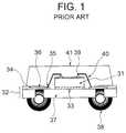
- FIG. 1shows the structure of a conventional BGA semiconductor device, wherein a semiconductor chip 31 is mounted on a central area of an interposer substrate 32 , and fixed to the interposer substrate 32 with the bottom surface of the semiconductor chip 31 being adhered thereto.
- the interposer substrate 32is made of an organic insulating substance such as polyimide, glass epoxy, BT resin etc, on which a metallic interconnect pattern or bonding pad 34 made of Cu, for example, is provided.
- the interposer substrate 32has a plurality of bonding pads 34 in the vicinity of the outer periphery thereof, i.e., outside the area for mounting the semiconductor chip 31 .
- the inner side 35 of the bonding pad 34is called stitch area and used for connection with a bonding wire 40
- the outer side 36 of the bonding pad 34is called land area on which a solder ball 38 is formed.
- the organic insulator 37 of the interposer substrate 32has an opening for the land area 36 , on the bottom surface of which the solder ball 38 is formed.
- the solder ball 38is used as an external terminal by an end user for mounting the semiconductor device on a printed circuit board.
- the mounting of the semiconductor chip 31 onto the interposer substrate 32is conducted as follows. First, a specified amount of adhesive 33 is dropped onto a specified position of the interposer substrate 32 from a multi-nozzle coater, then a semiconductor chip 31 is mounted thereto, and the adhesive 33 is cured by heating to fix the semiconductor chip 31 onto the interposer substrate 32 . Subsequently, Al chip electrodes 39 and the stitch area 35 of the bonding pads 34 are electrically connected together by a wire bonding technique using bonding wires 40 made of Au or Cu.
- the top surface of the interposer substrate 32 together with the semiconductor chip 31is encapsulated by a transfer molding technique using a mold resin 41 containing therein an epoxy resin as a main component thereof, whereby the semiconductor chip 31 is protected against mechanical damages thereof and ingress of moisture.
- solder balls 38 constituting external terminalsare formed on the bottom surfaces of the land areas 36 of the bonding pads 34 on the interposer substrate 32 .
- fluxis applied onto the land areas 36 beforehand, then the solder balls 38 are placed onto the land areas 36 , followed by thermal reflow of the solder ball 38 to form the external terminals 38 therefrom.
- the external terminals 38are made of solder including tin and lead as the main components thereof, for example.
- the two layer structure of the interposer substrate including the organic insulator and the metallic interconnect patternprevents a reduction of the thickness of the BGA semiconductor device having the interposer substrate.
- Patent Publications JP-A-2-240940, -10-116935 and -11-195733describes a technique for reducing the thickness of the semiconductor device by polishing the interposer substrate made of resin at the bottom surface thereof.
- an electrolytic plating techniquewhich allows formation of a metallic interconnect layer having a higher impurity is difficult to use on the resin interposer substrate.
- an electrolytic plating techniquecan be used on the resin substrate by providing an electrode film on the resin substrate, the electrode film must extend to the outer periphery of the resin substrate and thus forms the metallic interconnect pattern at the outer periphery where the metallic interconnect pattern is not needed.
- the locations of the land areas for the bonding padsare determined accordingly at the outside of the stitch areas. This imposes a large restriction on the arrangement of the external terminals, and causes an obstacle against the reduction of the planar dimensions of the electronic appliances or electronic parts mounting thereon the semiconductor device.
- the present inventionprovides, in a first aspect thereof, a semiconductor device including a semiconductor chip having chip electrodes thereon, a metallic interconnect pattern having a top surface connected to the chip electrodes and supporting the semiconductor chip, at least the top surface of the metallic interconnect pattern being formed by an electrolytic plating technique, a insulating film covering a bottom surface of the metallic interconnect pattern and having through-holes therein, a plurality of external terminals formed on the bottom surface of the interconnect pattern in the through-holes, and a mold resin encapsulating the semiconductor chip on the top surface of the metallic interconnect pattern and the insulating film.
- the semiconductor device of the present inventionby employing a structure wherein only a thin insulator film and an electrolytic-plated interconnect pattern are formed on the bottom surface of the semiconductor chip, the overall thickness of the semiconductor device can be reduced compared to the conventional semiconductor device having the interposer substrate.
- the electrolytic-plated interconnect patternhas an improved reliability, thereby allowing improvements in quality and reduction of dimensions and costs for the electronic appliances and parts mounting thereon the semiconductor device.
- the present inventionalso provides, in a second aspect thereof, a method for forming a semiconductor device including the steps of forming a frame substrate having a metallic plate and a metallic interconnect pattern formed on a top surface of the metallic plate, mounting a semiconductor chip on the interconnect pattern, encapsulating the semiconductor chip on the frame substrate by a mold resin, and removing at least a part of the metallic plate at a bottom surface thereof to expose at least a part of the metallic interconnect pattern.
- the process of removing the metallic plate of the frame substrate to expose the interconnect pattern after encapsulating the semiconductor chip by a mold resinassures an excellent rigidity of the semiconductor device before the encapsulation and reduces the overall thickness of the semiconductor device after the encapsulation.
- FIG. 1is a sectional view of a conventional BGA semiconductor device having an interposer substrate.
- FIG. 2is a sectional view of a semiconductor device according to an embodiment of the present invention.
- FIGS. 3A to 3 Dare sectional views of the frame substrate shown in of FIG. 2, showing consecutive steps of a method for fabrication thereof.
- FIGS. 4A to 4 Dare sectional views of the frame substrate shown in FIG. 2, for showing consecutive steps of another method for fabrication thereof.
- FIGS. 5A to 5 Gare sectional views of the semiconductor device of FIG. 2, showing consecutive steps of a method for fabrication thereof according to a first embodiment of the present invention.
- FIGS. 6A to 6 Gare sectional views of a semiconductor device, showing consecutive steps of a method for fabrication thereof according to a second embodiment of the present invention.
- FIGS. 7A to 7 Fare sectional views of a semiconductor device, showing consecutive steps of a method for fabrication thereof according to a third embodiment of the present invention.
- FIGS. 8A to 8 Fare sectional views of a semiconductor device, showing consecutive steps of a method for fabrication thereof according to a fourth embodiment of the present invention.
- FIGS. 9A to 9 Fare sectional views of a semiconductor device, showing consecutive steps of a method for fabrication thereof according to a fifth embodiment of the present invention.
- FIGS. 10A to 10 Fare sectional views of a semiconductor device, showing consecutive steps of a method for fabrication thereof according to a sixth embodiment of the present invention.
- FIGS. 11A to 11 Dare sectional views of a semiconductor device, showing consecutive steps of a method for fabrication thereof according to a seventh embodiment of the present invention.
- FIGS. 12A to 12 Dare sectional views of a semiconductor device, showing consecutive steps of a method for fabrication thereof according to an eighth embodiment of the present invention.
- FIG. 13is a sectional view of a semiconductor device according to another embodiment of the present invention.
- FIG. 14is a sectional view of a semiconductor device according to another embodiment of the present invention.
- FIG. 15is a sectional view of a semiconductor device according to another embodiment of the present invention.
- a semiconductor deviceincludes a semiconductor chip 15 encapsulated by a transfer molding technique using a mold resin 17 .
- the semiconductor chip 15is fixed onto a metallic film pattern 14 , or die pad, in the central area thereof, with the bottom of the semiconductor chip 15 fixed thereto using an insulating adhesive layer 20 .
- Each of the chip electrodes 26 formed on the semiconductor chip 15is connected to a stitch area of the metallic film pattern 14 disposed at the outer side of the semiconductor chip 15 .
- a plurality of land patterns 13are disposed on the bottom surface of the metallic film pattern 14 .
- the land patterns 13are formed by patterning a metallic plate, and a solder ball 18 is formed on the bottom of each of the land patterns 13 .
- An insulating adhesive layer 19is formed by coating on the entire bottom surface of the semiconductor device except for the land patterns 13 .
- the land patterns 13may be omitted, with the solder balls 18 disposed directly on the bottom of the metallic interconnect pattern 14 , which further reduces the overall thickness of the final semiconductor device.
- solder balls (first solder balls) 18are disposed on the inner side of the metallic interconnect pattern 14 just below the semiconductor chip 15 , whereas the others of the solder balls (second solder balls) 18 are disposed on the outer side of the metallic interconnect pattern 14 outside the semiconductor chip 15 as viewed on the bottom surface of the semiconductor device.
- the first solder balls 18 and the second solder balls 18are disposed alternately with each other.
- the first solder balls 18are disposed just below the outer periphery of the semiconductor chip 15 .
- the second solder balls 18are disposed just below the stitch areas connected to the bonding wires 16 .
- the alternate arrangement of the first solder balls 18 and the second solder balls 18allows a smaller pitch of the solder balls 18 without interference therebetween.
- FIGS. 3A to 3 Dshow a process for forming the frame substrate used for fabricating the semiconductor device of FIG. 2 .
- a metallic plate 11is first prepared, on which a resist film 12 is formed by coating, followed by patterning thereof to form a negative resist pattern 12 which is negative with respective to a desired interconnect pattern, as shown in FIG. 3B.
- a metallic interconnect pattern 14is then formed on the exposed surface of the metallic plate 11 by a plating technique, as shown in FIG. 3C, followed by removal of the negative resist pattern 12 to obtain a frame substrate wherein a metallic interconnect pattern 14 is formed on the metallic plate 11 , as shown in FIG. 3 D.
- FIGS. 4A to 4 Dshow another process for forming the frame substrate used for fabrication of the semiconductor device of FIG. 2 .
- a metallic plate 11is first prepared, followed by forming thereon a positive resist pattern 12 , which is positive with respect to a desired interconnect pattern.
- the metallic plate 11is then etched using the positive resist pattern 12 as an etching mask, as shown in FIG. 4C, followed by removal of the positive resist pattern 12 from the metallic plate 11 .
- a frame substrate 13is obtained wherein a land pattern 14 is formed as a metallic interconnect pattern on the top surface of the metallic plate 11 .
- FIGS. 5A to 5 Gshow a fabrication process for a semiconductor device according to a first embodiment of the present invention.
- a frame substrate(or may be called temporary interposer substrate) wherein a metallic pattern 14 is formed on a metallic plate 11 is prepared by a process such as shown in FIGS. 3A to 3 D.
- a semiconductor chip 15the bottom of which is applied with adhesive 20 , is mounted on the frame substrate, with the outer periphery of the semiconductor chip 15 being placed on the inner side of the metallic pattern 14 of the frame substrate, as shown in FIG. 5 B.
- the chip electrodes 26 on the semiconductor chip 15are electrically connected to the stitch areas disposed outer side of the metallic pattern 14 by bonding wires 16 , as shown in FIG. 5C, followed by encapsulating the semiconductor chip 15 on the top surface of the frame substrate by a transfer molding technique using a mold resin 17 .
- the metallic plate 11 of the frame substrateis removed at the bottom surface thereof by wet etching or a plasma etching, to leave land patterns 13 on the bottom surface of the metallic interconnect pattern 14 .
- the land patterns 13can be formed with ease at either the outer or inner side of the metallic interconnect pattern 14 , whereby design choice for the locations of the land patterns 13 can be improved.
- an insulating adhesiveis applied to the patterned surface to form an adhesive layer 19 , through which the land patterns 13 penetrate, as shown in FIG. 5 F. Then, a solder ball 18 is formed on each of the land patterns 13 , to obtain the structure shown in FIG. 5 G.
- solder balls 18are disposed alternately at the inner side and at the outer side of the metallic pattern 14 in the present embodiment. In alternative, the solder balls 18 may be disposed in a checkered pattern on the bottom surface. This configuration allows the external terminals to be disposed in the substantially entire bottom area of the semiconductor device, thereby reducing the planar dimensions of the semiconductor device.
- the order of coating the insulating adhesive 19 and forming the solder balls 18may be reversed from the recited order.
- the solder balls 18may be omitted, with the terminals of the electronic appliances or parts directly mounting the land patterns 13 by using another known technique.
- the metallic plate 11may be polished by a CMP process without leaving the land patterns 13 .
- the solder balls 18may be formed directly on the bottom surface of the metallic interconnect pattern 14 .
- FIGS. 6A to 6 Gconsecutively show another process for fabrication of a semiconductor device according to a second embodiment of the present invention.
- the processincludes the steps of forming the frame substrate.
- an insulating adhesive layer 21is formed on a metallic plate 11 by coating, followed by patterning thereof to form openings 22 in the adhesive layer 21 , as shown in FIG. 6 B.
- the openings 22which are to receive therein solder balls are arranged in a row underlying the outer periphery of the semiconductor chip to be placed, and another row outside the area mounting thereon the semiconductor chip. Two rows of the openings 22 are disposed in a staggered arrangement.
- a metallic film 23is adhered onto the insulating adhesive layer 21 , as shown in FIG. 6C, followed by patterning of the metallic film 23 to form therein a central opening 24 as well as to form a metallic interconnect pattern therefrom, as shown in FIG. 6 D.
- An insulating adhesive 25is then applied in the central opening 22 , and a semiconductor chip 15 having a bottom onto which a similar insulating adhesive 25 is applied is placed on the metallic interconnect pattern 23 so that the center of the semiconductor chip 15 is aligned with the center of the central opening 22 .
- the chip electrodes 26 on the semiconductor chip 15are electrically connected to the metallic interconnect pattern 23 by bonding wires 16 , as shown in FIG. 6 E.
- the semiconductor chip 15is encapsulated on top of the metallic interconnect pattern 23 and the insulating film 11 by a transfer molding using a mold resin 17 , as shown in FIG. 6 F.
- the metallic plate 11is removed by etching, such as chemical etching using an etchant, plasma etching, chemical-mechanical polishing (CMP) using an abrasive etc.
- a solder ball 18is formed through each of the openings 22 on the bottom of the metallic interconnect pattern 23 , as shown in FIG. 6 G.
- the solder balls 18are disposed in a staggered arrangement or alternately at the inner side and the outer side of the metallic interconnect pattern 23 .
- the formation of the solder ball 18 through the opening 22can be conducted more easily compared to the first embodiment.
- removal of the step of forming the insulating adhesive layer after the removal of the metallic plate 11reduces the number of steps for the fabrication. It is to be noted that the arrangement of the solder balls 18 in the present embodiment of the present invention is a mere example, and may be modified therefrom.
- FIGS. 7A to 7 Fconsecutively show a method for fabricating a semiconductor device according to a third embodiment of the present invention.
- a metallic plate, or Cu plate, 51is subjected to etching the top surface thereof to form an interconnect pattern 52 , which includes a pattern portion acting as a support member for supporting a semiconductor chip.
- the pattern portionis located at the central area of the Cu plate 51 .
- an insulating adhesive 53is applied onto the top of the Cu plate 52 at the central pattern portion, followed by mounting thereon a semiconductor chip 54 to be adhered, as shown in FIG. 7 B.
- Chip electrodes 55 on the semiconductor chip 54are connected to the interconnect pattern 52 by bonding wires 56 , as shown in FIG. 7 C.
- a transfer molding processis performed using a mold resin 57 for encapsulation of the semiconductor chip 54 as well as the bonding wires 56 onto the top of the Cu plate 51 , as shown in FIG. 7 D.
- the Cu plate 51is subjected to polishing at the bottom surface thereof to remove the portion of the Cu plate other than the interconnect pattern 52 , as shown in FIG. 7 E.
- An insulating sheet 58is then adhered onto the interconnect pattern 52 at the bottom thereof, followed by forming metallic bumps 59 on the interconnect pattern 52 , metallic bumps 59 penetrating the insulating sheet 58 at through-holes, as shown in FIG. 7 G.
- the metallic bumps 59are located just below the periphery of the semiconductor chip 54 as well as outside the semiconductor chip 54 .
- the interconnect pattern 52is formed directly from the top of the Cu plate 51 .
- the interconnect patternmay be formed by the steps of forming grooves having a positive pattern for an interconnect pattern on the a metallic plate, and filling the grooves with a metallic plating film by using a electrolytic plating technique. The metallic plate is later removed by polishing and a selective wet etching at the bottom thereof.
- FIGS. 8A to 8 Fconsecutively show a method for fabricating a semiconductor device according to a fourth embodiment of the present invention.
- This embodimentis similar to the third embodiment except that the central portion of the metallic pattern 52 is used solely to support the semiconductor chip in the present embodiment, and the peripheral portion of the metallic pattern 52 is used as external electrodes and has a somewhat larger thickness for mechanical strength after the polishing thereof.
- the peripheral portion of the metallic pattern 52is mechanically configured and subjected to coating for forming an insulation film 60 thereon at the final step of fabrication.
- the peripheral portionis used as external lead wires.
- FIGS. 9A to 9 Fconsecutively show a method for fabricating a semiconductor device according to a fifth embodiment.
- an interconnect pattern 52is formed on a metallic plate 51 by etching.
- a semiconductor chip 54 having a face-down structureis mounted on the metallic plate 51 , with the chip electrodes 55 on the semiconductor chip 54 being in contact with the interconnect pattern 52 , as shown in FIG. 9 B.
- the top portion of the mold resin 57 as well as the top portion of the semiconductor chip 54is removed by mechanical grinding, as shown in FIG. 9 D.
- the bottom of the metallic plate 51is also removed by mechanical grinding to leave the interconnect pattern 52 as shown in FIG. 9E, followed by adhering an insulating sheet 58 on the bottom of the interconnect pattern 52 and forming metallic bumps 59 thereon, as shown in FIG. 9 F.
- FIGS. 10A to 10 Fconsecutively show a method for fabricating a semiconductor device according to a sixth embodiment of the present invention.
- the present embodimentis similar to the fifth embodiment except that the interconnect pattern 52 is used as external terminals lead wires in the present embodiment similarly to the fourth embodiment.
- FIGS. 11A to 11 Dshow a method for fabricating a semiconductor device according to a seventh embodiment of the present invention.
- the seventh embodimentis similar to the fifth embodiment except that metallic bumps 61 are provided on the chip electrodes 55 of the semiconductor chip 54 for connection with the interconnect pattern 52 on the metallic plate 51 in the present embodiment.
- FIGS. 12A to 12 Dconsecutively show a method for fabricating a semiconductor device according to an eighth embodiment of the present invention.
- the present embodimentis similar to the sixth embodiment except that an injection hole 62 is formed in the center of the metallic plate 51 in the present embodiment.
- the injection hole 62is formed before or after forming the interconnect pattern 52 and used later for injection of mold resin.
- a semiconductor deviceincludes first and second semiconductor chips 54 A and 54 B mounted on the top of an interconnect pattern 52 and encapsulated by a common mold resin 57 A.
- a third semiconductor chip 54 Cis mounted on the bottom of the interconnect pattern 52 , opposing the first semiconductor chip 54 A.
- the third semiconductor chip 54 Cis encapsulated by another mold resin 57 B.
- a fourth semiconductor chip 54 Dis mounted and encapsulated by another mold resin 57 C similarly to the semiconductor chip 54 C, opposing to the second semiconductor chip 54 B.
- the interconnect pattern 52is formed directly on the metallic plate 51 by etching the top of the metallic plate 51 .
- an over-etchingmay occur wherein the metallic interconnect pattern 52 is also removed.
- the metallic interconnect pattern 52 and the metallic plate 51are made of different metals.
- the metallic plate 51can be removed by a wet etching step selectively from the metallic interconnect pattern 52 .
- either of the metallic plate 51 and the metallic interconnect pattern 52is added with an additive so that both have different etching rates in a common etchant.
- a semiconductor deviceincludes a metallic plate 51 having a bottom layer 51 a made of a first metal and a top layer 51 b made of a second metal.
- the metallic interconnect pattern 52is also made of the first metal.
- the first metal and the second metalcan be etched by using different etchants.
- the top layeris etched by a second etchant selectively from the metallic interconnect pattern 52 .
- the metallic interconnect pattern 52may have at the bottom thereof another metallic film for enhancing the rigidity.
- a semiconductor device modified from the embodiment of FIG. 14includes a single metallic plate 51 made of a first metal, a metallic interconnect pattern 52 including a thin bottom layer 52 a made of a second metal and a thick top layer 52 b made of a third metal.
- the second and third metalsare formed by an electrolytic plating technique, for example.
- the electrolytic plating techniqueis superior to the electroless plating technique in view of a lower cost and a higher impurity of the resultant film. The higher impurity provides a superior connection capability.
- the metallic plate 51can be removed by chemical etching, physical (chemical-mechanical) polishing, mechanical grinding, mechanical peeling-off etc.
- the mechanical peeling-offmay be associated with provision of different metals having different coefficients of thermal expansion or different melting points.
- the metallic plate or layermay be made of Cu, Ni or Fe, for example.
- the adhesive or mold resinmay preferably include a thermo-curable epoxy resin as the main component thereof.
- solder ballscan be used which include Sn and Pb as the main components thereof.
- the frame substrate as used in the embodiments of the present inventionhas an advantage over the conventional interposer substrate, as will be detailed below.
- the metallic interconnect pattern formed by the electrolytic plating techniquegenerally has a higher impurity and achieves a superior connection capability.
- the metallic interconnect patterncan be formed by the electrolytic plating technique by using an electrode layer formed on the resin substrate.
- the electrode layermust extend to the outer periphery of the resin substrate for supplying electricity during the plating.
- the metallic interconnect patternis formed on the periphery at which the interconnect pattern is not needed.
- the metallic interconnect pattern formed on the peripherymay be exposed at the surface of the mold resin to be subjected to ingress of water. This deteriorates the insulation characteristics or corrosion of the metallic interconnect pattern in the resultant semiconductor device.
- the metallic interconnect pattern in the present inventioncan be formed by the electrolytic plating technique at the desired location on the metallic plate. This prevents deterioration or corrosion as encountered in the conventional interposer substrate.
Landscapes
- Engineering & Computer Science (AREA)
- Microelectronics & Electronic Packaging (AREA)
- Computer Hardware Design (AREA)
- Power Engineering (AREA)
- Physics & Mathematics (AREA)
- Condensed Matter Physics & Semiconductors (AREA)
- General Physics & Mathematics (AREA)
- Manufacturing & Machinery (AREA)
- Encapsulation Of And Coatings For Semiconductor Or Solid State Devices (AREA)
- Moulds For Moulding Plastics Or The Like (AREA)
- Structures Or Materials For Encapsulating Or Coating Semiconductor Devices Or Solid State Devices (AREA)
- Wire Bonding (AREA)
Abstract
Description
Claims (1)
Applications Claiming Priority (4)
| Application Number | Priority Date | Filing Date | Title |
|---|---|---|---|
| JP26195999 | 1999-09-16 | ||
| JP11-261959 | 1999-09-16 | ||
| JP2000-184151 | 2000-06-20 | ||
| JP2000184151AJP2001156212A (en) | 1999-09-16 | 2000-06-20 | Resin sealed semiconductor device and producing method therefor |
Publications (1)
| Publication Number | Publication Date |
|---|---|
| US6611063B1true US6611063B1 (en) | 2003-08-26 |
Family
ID=26545318
Family Applications (1)
| Application Number | Title | Priority Date | Filing Date |
|---|---|---|---|
| US09/664,061Expired - Fee RelatedUS6611063B1 (en) | 1999-09-16 | 2000-09-18 | Resin-encapsulated semiconductor device |
Country Status (7)
| Country | Link |
|---|---|
| US (1) | US6611063B1 (en) |
| JP (1) | JP2001156212A (en) |
| KR (1) | KR100383112B1 (en) |
| CN (1) | CN1289147A (en) |
| GB (2) | GB2360629B (en) |
| SG (1) | SG97935A1 (en) |
| TW (1) | TW463272B (en) |
Cited By (44)
| Publication number | Priority date | Publication date | Assignee | Title |
|---|---|---|---|---|
| US20040063242A1 (en)* | 2002-09-17 | 2004-04-01 | Chippac, Inc. | Semiconductor multi-package module having package stacked over ball grid array package and having wire bond interconnect between stacked packages |
| US20040061213A1 (en)* | 2002-09-17 | 2004-04-01 | Chippac, Inc. | Semiconductor multi-package module having package stacked over die-up flip chip ball grid array package and having wire bond interconnect between stacked packages |
| US20040195668A1 (en)* | 2003-02-06 | 2004-10-07 | Toshihiro Sawamoto | Semiconductor device, electronic device, electronic equipment, method of manufacturing semiconductor device, and method of manufacturing electronic device |
| US20040217380A1 (en)* | 2003-02-25 | 2004-11-04 | Akiyoshi Aoyagi | Semiconductor device, electronic device, electronic apparatus, method for manufacturing a semiconductor device, and method for manufacturing an electronic device |
| US20040222508A1 (en)* | 2003-03-18 | 2004-11-11 | Akiyoshi Aoyagi | Semiconductor device, electronic device, electronic apparatus, method of manufacturing semiconductor device, and method of manufacturing electronic device |
| US20040222510A1 (en)* | 2003-03-24 | 2004-11-11 | Akiyoshi Aoyagi | Semiconductor device, semiconductor pack age, electronic device, electronic apparatus, and manufacturing methods of semiconductor device and electronic device |
| US20040222534A1 (en)* | 2003-02-07 | 2004-11-11 | Toshihiro Sawamoto | Semiconductor device, electronic device, electronic equipment, method of manufacturing semiconductor device, and method of manufacturing electronic device |
| US20040222519A1 (en)* | 2003-03-18 | 2004-11-11 | Akiyoshi Aoyagi | Semiconductor device, electronic device, electronic apparatus, method of manufacturing semiconductor device, and method of manufacturing electronic device |
| US20040227236A1 (en)* | 2003-03-17 | 2004-11-18 | Toshihiro Sawamoto | Semiconductor device, electronic device, electronic apparatus, and methods for manufacturing carrier substrate, semiconductor device, and electronic device |
| US20040227223A1 (en)* | 2003-03-17 | 2004-11-18 | Toshihiro Sawamoto | Semiconductor device, electronic device, electronic apparatus, and methods for manufacturing semiconductor device and electronic device |
| US20050110166A1 (en)* | 2003-03-18 | 2005-05-26 | Akiyoshi Aoyagi | Semiconductor device, electronic device, electronic apparatus, method of manufacturing semiconductor device, and method of manufacturing electronic device |
| US20050110155A1 (en)* | 2003-10-24 | 2005-05-26 | Seiko Epson Corporation | Semiconductor device and method of manufacturing the same, circuit board and electronic device |
| US20050133916A1 (en)* | 2003-12-17 | 2005-06-23 | Stats Chippac, Inc | Multiple chip package module having inverted package stacked over die |
| US20050184379A1 (en)* | 2003-03-25 | 2005-08-25 | Masakuni Shiozawa | Semiconductor device, electronic device, electronic apparatus, and method of manufacturing semiconductor device |
| US20060012018A1 (en)* | 2004-07-13 | 2006-01-19 | Chippac, Inc. | Semiconductor multipackage module including die and inverted land grid array package stacked over ball grid array package |
| US7053476B2 (en) | 2002-09-17 | 2006-05-30 | Chippac, Inc. | Semiconductor multi-package module having package stacked over die-down flip chip ball grid array package and having wire bond interconnect between stacked packages |
| US7064426B2 (en) | 2002-09-17 | 2006-06-20 | Chippac, Inc. | Semiconductor multi-package module having wire bond interconnect between stacked packages |
| US20060220210A1 (en)* | 2005-03-31 | 2006-10-05 | Stats Chippac Ltd. | Semiconductor assembly including chip scale package and second substrate and having exposed substrate surfaces on upper and lower sides |
| US20060220209A1 (en)* | 2005-03-31 | 2006-10-05 | Stats Chippac Ltd. | Semiconductor stacked package assembly having exposed substrate surfaces on upper and lower sides |
| US20060244117A1 (en)* | 2005-04-29 | 2006-11-02 | Stats Chippac, Ltd. | Semiconductor package including second substrate and having exposed substrate surfaces on upper and lower sides |
| US20060249851A1 (en)* | 2005-05-05 | 2006-11-09 | Stats Chippac Ltd. | Multiple Chip Package Module Including Die Stacked Over Encapsulated Package |
| US20060284299A1 (en)* | 2005-06-20 | 2006-12-21 | Stats Chippac Ltd. | Module Having Stacked Chip Scale Semiconductor Packages |
| US20070018296A1 (en)* | 2004-05-24 | 2007-01-25 | Chippac, Inc | Stacked Semiconductor Package having Adhesive/Spacer Structure and Insulation |
| US20070111389A1 (en)* | 2005-04-22 | 2007-05-17 | Stats Chippac Ltd. | Micro chip-scale-package system |
| US20070111388A1 (en)* | 2002-10-08 | 2007-05-17 | Chippac, Inc. | Semiconductor Multi-Package Module Having Inverted Second Package Stacked Over Die-Up Flip-Chip Ball Grid Array (BGA) Package |
| US20070164418A1 (en)* | 2006-01-12 | 2007-07-19 | Infineon Technologies Ag | Semiconductor Module Comprising Semiconductor Chips and Method for Producing the Same |
| US20080054424A1 (en)* | 2006-08-31 | 2008-03-06 | Semiconductor Components Industries, Llc. | Semiconductor package and method therefor |
| US20080169549A1 (en)* | 2005-04-29 | 2008-07-17 | Flynn Carson | Stacked integrated circuit package system and method of manufacture therefor |
| US7652376B2 (en) | 2006-01-04 | 2010-01-26 | Stats Chippac Ltd. | Integrated circuit package system including stacked die |
| US7749807B2 (en) | 2003-04-04 | 2010-07-06 | Chippac, Inc. | Method of fabricating a semiconductor multipackage module including a processor and memory package assemblies |
| US7750482B2 (en) | 2006-02-09 | 2010-07-06 | Stats Chippac Ltd. | Integrated circuit package system including zero fillet resin |
| US7768125B2 (en) | 2006-01-04 | 2010-08-03 | Stats Chippac Ltd. | Multi-chip package system |
| US20100270665A1 (en)* | 2009-04-28 | 2010-10-28 | Macronix International Co., Ltd. | Leadframe |
| US7855100B2 (en) | 2005-03-31 | 2010-12-21 | Stats Chippac Ltd. | Integrated circuit package system with an encapsulant cavity and method of fabrication thereof |
| US20120061843A1 (en)* | 2010-09-13 | 2012-03-15 | Hynix Semiconductor Inc. | Semiconductor package and method for manufacturing the same |
| US8552551B2 (en) | 2004-05-24 | 2013-10-08 | Chippac, Inc. | Adhesive/spacer island structure for stacking over wire bonded die |
| US8623704B2 (en) | 2004-05-24 | 2014-01-07 | Chippac, Inc. | Adhesive/spacer island structure for multiple die package |
| US8704349B2 (en) | 2006-02-14 | 2014-04-22 | Stats Chippac Ltd. | Integrated circuit package system with exposed interconnects |
| US20150011053A1 (en)* | 2012-09-11 | 2015-01-08 | Freescale Semiconductor, Inc. | Semiconductor device and method of assembling same |
| TWI501371B (en)* | 2009-01-13 | 2015-09-21 | Dainippon Printing Co Ltd | A wiring member for a semiconductor device, a composite wiring member for a semiconductor device, and a resin-sealed type semiconductor device |
| US9324641B2 (en) | 2012-03-20 | 2016-04-26 | Stats Chippac Ltd. | Integrated circuit packaging system with external interconnect and method of manufacture thereof |
| US20160317068A1 (en)* | 2015-04-30 | 2016-11-03 | Verily Life Sciences Llc | Electronic devices with encapsulating silicone based adhesive |
| US20200203242A1 (en)* | 2018-12-19 | 2020-06-25 | Texas Instruments Incorporated | Low cost reliable fan-out fan-in chip scale package |
| US11133296B2 (en)* | 2016-11-21 | 2021-09-28 | Samsung Electronics Co., Ltd. | Semiconductor package |
Families Citing this family (10)
| Publication number | Priority date | Publication date | Assignee | Title |
|---|---|---|---|---|
| JP3801188B2 (en)* | 2004-09-06 | 2006-07-26 | セイコーエプソン株式会社 | Semiconductor device and manufacturing method of semiconductor device |
| CN100442465C (en)* | 2005-09-15 | 2008-12-10 | 南茂科技股份有限公司 | Chip packaging body process without core dielectric layer |
| KR100823224B1 (en)* | 2006-08-02 | 2008-04-18 | 주식회사 심텍 | Semiconductor Package Printed Circuit Board Forming Micro Bump and Manufacturing Method Thereof |
| KR100802393B1 (en)* | 2007-02-15 | 2008-02-13 | 삼성전기주식회사 | Package board and its manufacturing method |
| JP4605176B2 (en)* | 2007-04-20 | 2011-01-05 | 日立化成工業株式会社 | Semiconductor mounting substrate, semiconductor package manufacturing method, and semiconductor package |
| JP4605177B2 (en)* | 2007-04-20 | 2011-01-05 | 日立化成工業株式会社 | Semiconductor mounting substrate |
| TWI445100B (en) | 2011-05-20 | 2014-07-11 | Subtron Technology Co Ltd | Package structure and manufacturing method thereof |
| CN102376672B (en)* | 2011-11-30 | 2014-10-29 | 江苏长电科技股份有限公司 | Foundation island-free ball grid array packaging structure and manufacturing method thereof |
| US20130234330A1 (en)* | 2012-03-08 | 2013-09-12 | Infineon Technologies Ag | Semiconductor Packages and Methods of Formation Thereof |
| DE102019127791B4 (en)* | 2019-10-15 | 2022-09-01 | Infineon Technologies Ag | Package with separate substrate sections and method for manufacturing a package |
Citations (24)
| Publication number | Priority date | Publication date | Assignee | Title |
|---|---|---|---|---|
| JPH02151496A (en) | 1988-12-05 | 1990-06-11 | Matsushita Electric Ind Co Ltd | Method of manufacturing integrated circuit device |
| JPH02240940A (en) | 1989-03-15 | 1990-09-25 | Matsushita Electric Ind Co Ltd | Manufacture of integrated circuit device |
| EP0582052A1 (en) | 1992-08-06 | 1994-02-09 | Motorola, Inc. | Low profile overmolded semiconductor device and method for making the same |
| WO1995026047A1 (en) | 1994-03-18 | 1995-09-28 | Hitachi Chemical Company, Ltd. | Semiconductor package manufacturing method and semiconductor package |
| US5592025A (en) | 1992-08-06 | 1997-01-07 | Motorola, Inc. | Pad array semiconductor device |
| JPH09283925A (en) | 1996-04-16 | 1997-10-31 | Toppan Printing Co Ltd | Semiconductor device and manufacturing method thereof |
| US5726489A (en)* | 1994-09-30 | 1998-03-10 | Nec Corporation | Film carrier semiconductor device |
| US5729432A (en) | 1995-07-05 | 1998-03-17 | Anam Industrial Col, Ltd. | Ball grid array semiconductor package with improved heat dissipation and dehumidification effect |
| JPH10116935A (en) | 1996-10-08 | 1998-05-06 | Fujitsu Ltd | Semiconductor device and manufacturing method thereof |
| US5793106A (en) | 1995-02-28 | 1998-08-11 | Hitachi, Ltd. | Semiconductor device |
| JPH10284544A (en) | 1997-04-10 | 1998-10-23 | Hitachi Ltd | Semiconductor device and manufacturing method thereof |
| US5837567A (en) | 1994-05-16 | 1998-11-17 | Hitachi, Ltd. | Lead frame and semiconductor device |
| US5847455A (en) | 1995-11-07 | 1998-12-08 | Vlsi Technology, Inc. | Molded leadframe ball grid array |
| US5874784A (en)* | 1995-10-25 | 1999-02-23 | Sharp Kabushiki Kaisha | Semiconductor device having external connection terminals provided on an interconnection plate and fabrication process therefor |
| US5905303A (en)* | 1994-05-25 | 1999-05-18 | Nec Corporation | Method for manufacturing bump leaded film carrier type semiconductor device |
| KR19990037053A (en) | 1997-10-13 | 1999-05-25 | 아끼구사 나오유끼 | Formation method of protruding electrode |
| JPH11195733A (en) | 1997-10-28 | 1999-07-21 | Seiko Epson Corp | Method of manufacturing semiconductor device, conductive plate for semiconductor device, and semiconductor device |
| US5990545A (en)* | 1996-12-02 | 1999-11-23 | 3M Innovative Properties Company | Chip scale ball grid array for integrated circuit package |
| US5990546A (en)* | 1994-12-29 | 1999-11-23 | Nitto Denko Corporation | Chip scale package type of semiconductor device |
| US6025650A (en)* | 1994-08-24 | 2000-02-15 | Fujitsu Limited | Semiconductor device including a frame terminal |
| US6204564B1 (en)* | 1997-11-21 | 2001-03-20 | Rohm Co., Ltd. | Semiconductor device and method for making the same |
| US6316838B1 (en)* | 1999-10-29 | 2001-11-13 | Fujitsu Limited | Semiconductor device |
| US6330166B1 (en)* | 1998-09-29 | 2001-12-11 | Denso Corporation | Electronic-component mounting structure |
| US6340606B1 (en)* | 1998-03-27 | 2002-01-22 | Seiko Epson Corporation | Semiconductor device and method of manufacturing the same, circuit board, and electronic instrument |
- 2000
- 2000-06-20JPJP2000184151Apatent/JP2001156212A/enactivePending
- 2000-09-15GBGB0022745Apatent/GB2360629B/ennot_activeExpired - Fee Related
- 2000-09-15GBGB0202655Apatent/GB2369245B/ennot_activeExpired - Fee Related
- 2000-09-15KRKR10-2000-0054182Apatent/KR100383112B1/ennot_activeExpired - Fee Related
- 2000-09-15CNCN00124859Apatent/CN1289147A/enactivePending
- 2000-09-15SGSG200005207Apatent/SG97935A1/enunknown
- 2000-09-15TWTW89118927Apatent/TW463272B/ennot_activeIP Right Cessation
- 2000-09-18USUS09/664,061patent/US6611063B1/ennot_activeExpired - Fee Related
Patent Citations (24)
| Publication number | Priority date | Publication date | Assignee | Title |
|---|---|---|---|---|
| JPH02151496A (en) | 1988-12-05 | 1990-06-11 | Matsushita Electric Ind Co Ltd | Method of manufacturing integrated circuit device |
| JPH02240940A (en) | 1989-03-15 | 1990-09-25 | Matsushita Electric Ind Co Ltd | Manufacture of integrated circuit device |
| EP0582052A1 (en) | 1992-08-06 | 1994-02-09 | Motorola, Inc. | Low profile overmolded semiconductor device and method for making the same |
| US5592025A (en) | 1992-08-06 | 1997-01-07 | Motorola, Inc. | Pad array semiconductor device |
| WO1995026047A1 (en) | 1994-03-18 | 1995-09-28 | Hitachi Chemical Company, Ltd. | Semiconductor package manufacturing method and semiconductor package |
| US5837567A (en) | 1994-05-16 | 1998-11-17 | Hitachi, Ltd. | Lead frame and semiconductor device |
| US5905303A (en)* | 1994-05-25 | 1999-05-18 | Nec Corporation | Method for manufacturing bump leaded film carrier type semiconductor device |
| US6025650A (en)* | 1994-08-24 | 2000-02-15 | Fujitsu Limited | Semiconductor device including a frame terminal |
| US5726489A (en)* | 1994-09-30 | 1998-03-10 | Nec Corporation | Film carrier semiconductor device |
| US5990546A (en)* | 1994-12-29 | 1999-11-23 | Nitto Denko Corporation | Chip scale package type of semiconductor device |
| US5793106A (en) | 1995-02-28 | 1998-08-11 | Hitachi, Ltd. | Semiconductor device |
| US5729432A (en) | 1995-07-05 | 1998-03-17 | Anam Industrial Col, Ltd. | Ball grid array semiconductor package with improved heat dissipation and dehumidification effect |
| US5874784A (en)* | 1995-10-25 | 1999-02-23 | Sharp Kabushiki Kaisha | Semiconductor device having external connection terminals provided on an interconnection plate and fabrication process therefor |
| US5847455A (en) | 1995-11-07 | 1998-12-08 | Vlsi Technology, Inc. | Molded leadframe ball grid array |
| JPH09283925A (en) | 1996-04-16 | 1997-10-31 | Toppan Printing Co Ltd | Semiconductor device and manufacturing method thereof |
| JPH10116935A (en) | 1996-10-08 | 1998-05-06 | Fujitsu Ltd | Semiconductor device and manufacturing method thereof |
| US5990545A (en)* | 1996-12-02 | 1999-11-23 | 3M Innovative Properties Company | Chip scale ball grid array for integrated circuit package |
| JPH10284544A (en) | 1997-04-10 | 1998-10-23 | Hitachi Ltd | Semiconductor device and manufacturing method thereof |
| KR19990037053A (en) | 1997-10-13 | 1999-05-25 | 아끼구사 나오유끼 | Formation method of protruding electrode |
| JPH11195733A (en) | 1997-10-28 | 1999-07-21 | Seiko Epson Corp | Method of manufacturing semiconductor device, conductive plate for semiconductor device, and semiconductor device |
| US6204564B1 (en)* | 1997-11-21 | 2001-03-20 | Rohm Co., Ltd. | Semiconductor device and method for making the same |
| US6340606B1 (en)* | 1998-03-27 | 2002-01-22 | Seiko Epson Corporation | Semiconductor device and method of manufacturing the same, circuit board, and electronic instrument |
| US6330166B1 (en)* | 1998-09-29 | 2001-12-11 | Denso Corporation | Electronic-component mounting structure |
| US6316838B1 (en)* | 1999-10-29 | 2001-11-13 | Fujitsu Limited | Semiconductor device |
Cited By (89)
| Publication number | Priority date | Publication date | Assignee | Title |
|---|---|---|---|---|
| US7205647B2 (en) | 2002-09-17 | 2007-04-17 | Chippac, Inc. | Semiconductor multi-package module having package stacked over ball grid array package and having wire bond interconnect between stacked packages |
| US20100200966A1 (en)* | 2002-09-17 | 2010-08-12 | Marcos Karnezos | Semiconductor multi-package module having package stacked over die-up flip chip ball grid array package and having wire bond interconnect between stacked packages |
| US7935572B2 (en) | 2002-09-17 | 2011-05-03 | Chippac, Inc. | Semiconductor multi-package module having package stacked over die-up flip chip ball grid array package and having wire bond interconnect between stacked packages |
| US20060170091A1 (en)* | 2002-09-17 | 2006-08-03 | Chippac, Inc. | Semiconductor multi-package module having package stacked over die-down flip chip ball grid array package and having wire bond interconnect between stacked packages |
| US7279361B2 (en) | 2002-09-17 | 2007-10-09 | Chippac, Inc. | Method for making a semiconductor multi-package module having wire bond interconnect between stacked packages |
| US8143100B2 (en) | 2002-09-17 | 2012-03-27 | Chippac, Inc. | Method of fabricating a semiconductor multi-package module having wire bond interconnect between stacked packages |
| US20040063242A1 (en)* | 2002-09-17 | 2004-04-01 | Chippac, Inc. | Semiconductor multi-package module having package stacked over ball grid array package and having wire bond interconnect between stacked packages |
| US20060172463A1 (en)* | 2002-09-17 | 2006-08-03 | Chippac, Inc. | Semiconductor multi-package module having wire bond interconnect between stacked packages |
| US20040061213A1 (en)* | 2002-09-17 | 2004-04-01 | Chippac, Inc. | Semiconductor multi-package module having package stacked over die-up flip chip ball grid array package and having wire bond interconnect between stacked packages |
| US7064426B2 (en) | 2002-09-17 | 2006-06-20 | Chippac, Inc. | Semiconductor multi-package module having wire bond interconnect between stacked packages |
| US7053476B2 (en) | 2002-09-17 | 2006-05-30 | Chippac, Inc. | Semiconductor multi-package module having package stacked over die-down flip chip ball grid array package and having wire bond interconnect between stacked packages |
| US7682873B2 (en) | 2002-09-17 | 2010-03-23 | Chippac, Inc. | Semiconductor multi-package module having package stacked over die-down flip chip ball grid array package and having wire bond interconnect between stacked packages |
| US20070111388A1 (en)* | 2002-10-08 | 2007-05-17 | Chippac, Inc. | Semiconductor Multi-Package Module Having Inverted Second Package Stacked Over Die-Up Flip-Chip Ball Grid Array (BGA) Package |
| US7687313B2 (en) | 2002-10-08 | 2010-03-30 | Stats Chippac Ltd. | Method of fabricating a semiconductor multi package module having an inverted package stacked over ball grid array (BGA) package |
| US7351610B2 (en) | 2002-10-08 | 2008-04-01 | Chippac, Inc. | Method of fabricating a semiconductor multi-package module having a second package substrate with an exposed metal layer wire bonded to a first package substrate |
| US7358115B2 (en) | 2002-10-08 | 2008-04-15 | Chippac, Inc. | Method of fabricating a semiconductor assembly including chip scale package and second substrate with exposed substrate surfaces on upper and lower sides |
| US20070114648A1 (en)* | 2002-10-08 | 2007-05-24 | Chippac, Inc. | Semiconductor Stacked Multi-Package Module Having Inverted Second Package |
| US20070117267A1 (en)* | 2002-10-08 | 2007-05-24 | Chippac, Inc. | Semiconductor Multi-Package Module Having Inverted Land Grid Array (LGA) Package Stacked Over Ball Grid Array (BGA) Package |
| US7364946B2 (en) | 2002-10-08 | 2008-04-29 | Chippac, Inc. | Method of fabricating a semiconductor multi-package module having inverted land grid array (LGA) package stacked over ball grid array (BGA) package |
| US20060125096A1 (en)* | 2003-02-05 | 2006-06-15 | Masakuni Shiozawa | Semiconductor device, electronic device, electronic apparatus, and method of manufacturing semiconductor device |
| US20040195668A1 (en)* | 2003-02-06 | 2004-10-07 | Toshihiro Sawamoto | Semiconductor device, electronic device, electronic equipment, method of manufacturing semiconductor device, and method of manufacturing electronic device |
| US7230329B2 (en) | 2003-02-07 | 2007-06-12 | Seiko Epson Corporation | Semiconductor device, electronic device, electronic equipment, method of manufacturing semiconductor device, and method of manufacturing electronic device |
| US20040222534A1 (en)* | 2003-02-07 | 2004-11-11 | Toshihiro Sawamoto | Semiconductor device, electronic device, electronic equipment, method of manufacturing semiconductor device, and method of manufacturing electronic device |
| US20040217380A1 (en)* | 2003-02-25 | 2004-11-04 | Akiyoshi Aoyagi | Semiconductor device, electronic device, electronic apparatus, method for manufacturing a semiconductor device, and method for manufacturing an electronic device |
| US20040227236A1 (en)* | 2003-03-17 | 2004-11-18 | Toshihiro Sawamoto | Semiconductor device, electronic device, electronic apparatus, and methods for manufacturing carrier substrate, semiconductor device, and electronic device |
| US20040227223A1 (en)* | 2003-03-17 | 2004-11-18 | Toshihiro Sawamoto | Semiconductor device, electronic device, electronic apparatus, and methods for manufacturing semiconductor device and electronic device |
| US20040222508A1 (en)* | 2003-03-18 | 2004-11-11 | Akiyoshi Aoyagi | Semiconductor device, electronic device, electronic apparatus, method of manufacturing semiconductor device, and method of manufacturing electronic device |
| US20040222519A1 (en)* | 2003-03-18 | 2004-11-11 | Akiyoshi Aoyagi | Semiconductor device, electronic device, electronic apparatus, method of manufacturing semiconductor device, and method of manufacturing electronic device |
| US20050110166A1 (en)* | 2003-03-18 | 2005-05-26 | Akiyoshi Aoyagi | Semiconductor device, electronic device, electronic apparatus, method of manufacturing semiconductor device, and method of manufacturing electronic device |
| US7091619B2 (en) | 2003-03-24 | 2006-08-15 | Seiko Epson Corporation | Semiconductor device, semiconductor package, electronic device, electronic apparatus, and manufacturing methods of semiconductor device and electronic device |
| US20040222510A1 (en)* | 2003-03-24 | 2004-11-11 | Akiyoshi Aoyagi | Semiconductor device, semiconductor pack age, electronic device, electronic apparatus, and manufacturing methods of semiconductor device and electronic device |
| US20050184379A1 (en)* | 2003-03-25 | 2005-08-25 | Masakuni Shiozawa | Semiconductor device, electronic device, electronic apparatus, and method of manufacturing semiconductor device |
| US7256072B2 (en) | 2003-03-25 | 2007-08-14 | Seiko Epson Corporation | Semiconductor device, electronic device, electronic apparatus, and method of manufacturing semiconductor device |
| US7749807B2 (en) | 2003-04-04 | 2010-07-06 | Chippac, Inc. | Method of fabricating a semiconductor multipackage module including a processor and memory package assemblies |
| US7235885B2 (en)* | 2003-10-24 | 2007-06-26 | Sieko Epson Corporation | Semiconductor device and method of manufacturing the same, circuit board and electronic device |
| US20050110155A1 (en)* | 2003-10-24 | 2005-05-26 | Seiko Epson Corporation | Semiconductor device and method of manufacturing the same, circuit board and electronic device |
| US20070235881A1 (en)* | 2003-10-24 | 2007-10-11 | Seiko Epson Corporation | Semiconductor Device and Method of Manufacturing the Same, Circuit Board and Electronic Device |
| US20050133916A1 (en)* | 2003-12-17 | 2005-06-23 | Stats Chippac, Inc | Multiple chip package module having inverted package stacked over die |
| US8970049B2 (en) | 2003-12-17 | 2015-03-03 | Chippac, Inc. | Multiple chip package module having inverted package stacked over die |
| US8030134B2 (en) | 2004-05-24 | 2011-10-04 | Chippac, Inc. | Stacked semiconductor package having adhesive/spacer structure and insulation |
| US20070018296A1 (en)* | 2004-05-24 | 2007-01-25 | Chippac, Inc | Stacked Semiconductor Package having Adhesive/Spacer Structure and Insulation |
| US8552551B2 (en) | 2004-05-24 | 2013-10-08 | Chippac, Inc. | Adhesive/spacer island structure for stacking over wire bonded die |
| US8623704B2 (en) | 2004-05-24 | 2014-01-07 | Chippac, Inc. | Adhesive/spacer island structure for multiple die package |
| US7253511B2 (en) | 2004-07-13 | 2007-08-07 | Chippac, Inc. | Semiconductor multipackage module including die and inverted land grid array package stacked over ball grid array package |
| US7829382B2 (en) | 2004-07-13 | 2010-11-09 | Chippac, Inc. | Method for making semiconductor multipackage module including die and inverted land grid array package stacked over ball grid array package |
| US20070278658A1 (en)* | 2004-07-13 | 2007-12-06 | Stats Chippac Ltd. | Semiconductor multipackage module including die and inverted land grid array package stacked over ball grid array package |
| US20100136744A1 (en)* | 2004-07-13 | 2010-06-03 | Marcos Karnezos | Method for making semiconductor multipackage module including die and inverted land grid array package stacked over ball grid array package |
| US7692279B2 (en) | 2004-07-13 | 2010-04-06 | Chippac, Inc. | Semiconductor multipackage module including die and inverted land grid array package stacked over ball grid array package |
| US20060012018A1 (en)* | 2004-07-13 | 2006-01-19 | Chippac, Inc. | Semiconductor multipackage module including die and inverted land grid array package stacked over ball grid array package |
| US20060220209A1 (en)* | 2005-03-31 | 2006-10-05 | Stats Chippac Ltd. | Semiconductor stacked package assembly having exposed substrate surfaces on upper and lower sides |
| US7372141B2 (en) | 2005-03-31 | 2008-05-13 | Stats Chippac Ltd. | Semiconductor stacked package assembly having exposed substrate surfaces on upper and lower sides |
| US20060220210A1 (en)* | 2005-03-31 | 2006-10-05 | Stats Chippac Ltd. | Semiconductor assembly including chip scale package and second substrate and having exposed substrate surfaces on upper and lower sides |
| US8309397B2 (en) | 2005-03-31 | 2012-11-13 | Stats Chippac Ltd. | Integrated circuit packaging system with a component in an encapsulant cavity and method of fabrication thereof |
| US8021924B2 (en) | 2005-03-31 | 2011-09-20 | Stats Chippac Ltd. | Encapsulant cavity integrated circuit package system and method of fabrication thereof |
| US7855100B2 (en) | 2005-03-31 | 2010-12-21 | Stats Chippac Ltd. | Integrated circuit package system with an encapsulant cavity and method of fabrication thereof |
| US7429787B2 (en) | 2005-03-31 | 2008-09-30 | Stats Chippac Ltd. | Semiconductor assembly including chip scale package and second substrate with exposed surfaces on upper and lower sides |
| US20070111389A1 (en)* | 2005-04-22 | 2007-05-17 | Stats Chippac Ltd. | Micro chip-scale-package system |
| US7652382B2 (en)* | 2005-04-22 | 2010-01-26 | Stats Chippac Ltd. | Micro chip-scale-package system |
| US7298052B2 (en)* | 2005-04-22 | 2007-11-20 | Stats Chippac Ltd. | Micro chip-scale-package system |
| US20080029861A1 (en)* | 2005-04-22 | 2008-02-07 | Jong Kook Kim | Micro chip-scale-package system |
| US7687315B2 (en) | 2005-04-29 | 2010-03-30 | Stats Chippac Ltd. | Stacked integrated circuit package system and method of manufacture therefor |
| US20080169549A1 (en)* | 2005-04-29 | 2008-07-17 | Flynn Carson | Stacked integrated circuit package system and method of manufacture therefor |
| US20060244117A1 (en)* | 2005-04-29 | 2006-11-02 | Stats Chippac, Ltd. | Semiconductor package including second substrate and having exposed substrate surfaces on upper and lower sides |
| US7429786B2 (en) | 2005-04-29 | 2008-09-30 | Stats Chippac Ltd. | Semiconductor package including second substrate and having exposed substrate surfaces on upper and lower sides |
| US7582960B2 (en) | 2005-05-05 | 2009-09-01 | Stats Chippac Ltd. | Multiple chip package module including die stacked over encapsulated package |
| US20060249851A1 (en)* | 2005-05-05 | 2006-11-09 | Stats Chippac Ltd. | Multiple Chip Package Module Including Die Stacked Over Encapsulated Package |
| US7645634B2 (en) | 2005-06-20 | 2010-01-12 | Stats Chippac Ltd. | Method of fabricating module having stacked chip scale semiconductor packages |
| US20060284299A1 (en)* | 2005-06-20 | 2006-12-21 | Stats Chippac Ltd. | Module Having Stacked Chip Scale Semiconductor Packages |
| US7394148B2 (en) | 2005-06-20 | 2008-07-01 | Stats Chippac Ltd. | Module having stacked chip scale semiconductor packages |
| US7652376B2 (en) | 2006-01-04 | 2010-01-26 | Stats Chippac Ltd. | Integrated circuit package system including stacked die |
| US7768125B2 (en) | 2006-01-04 | 2010-08-03 | Stats Chippac Ltd. | Multi-chip package system |
| US20070164418A1 (en)* | 2006-01-12 | 2007-07-19 | Infineon Technologies Ag | Semiconductor Module Comprising Semiconductor Chips and Method for Producing the Same |
| US7592689B2 (en)* | 2006-01-12 | 2009-09-22 | Infineon Technologies Ag | Semiconductor module comprising semiconductor chips and method for producing the same |
| US7750482B2 (en) | 2006-02-09 | 2010-07-06 | Stats Chippac Ltd. | Integrated circuit package system including zero fillet resin |
| US8704349B2 (en) | 2006-02-14 | 2014-04-22 | Stats Chippac Ltd. | Integrated circuit package system with exposed interconnects |
| US7638863B2 (en)* | 2006-08-31 | 2009-12-29 | Semiconductor Components Industries, Llc | Semiconductor package and method therefor |
| US7825505B2 (en)* | 2006-08-31 | 2010-11-02 | Semiconductor Components Industries, Llc | Semiconductor package and method therefor |
| US20080054424A1 (en)* | 2006-08-31 | 2008-03-06 | Semiconductor Components Industries, Llc. | Semiconductor package and method therefor |
| TWI501371B (en)* | 2009-01-13 | 2015-09-21 | Dainippon Printing Co Ltd | A wiring member for a semiconductor device, a composite wiring member for a semiconductor device, and a resin-sealed type semiconductor device |
| US20100270665A1 (en)* | 2009-04-28 | 2010-10-28 | Macronix International Co., Ltd. | Leadframe |
| US8133759B2 (en)* | 2009-04-28 | 2012-03-13 | Macronix International Co., Ltd. | Leadframe |
| US8846444B2 (en)* | 2010-09-13 | 2014-09-30 | SK Hynix Inc. | Semiconductor package and method for manufacturing the same |
| US20120061843A1 (en)* | 2010-09-13 | 2012-03-15 | Hynix Semiconductor Inc. | Semiconductor package and method for manufacturing the same |
| US9324641B2 (en) | 2012-03-20 | 2016-04-26 | Stats Chippac Ltd. | Integrated circuit packaging system with external interconnect and method of manufacture thereof |
| US20150011053A1 (en)* | 2012-09-11 | 2015-01-08 | Freescale Semiconductor, Inc. | Semiconductor device and method of assembling same |
| US9129948B2 (en)* | 2012-09-11 | 2015-09-08 | Freescale Semiconductor, Inc. | Semiconductor device and method of assembling same |
| US20160317068A1 (en)* | 2015-04-30 | 2016-11-03 | Verily Life Sciences Llc | Electronic devices with encapsulating silicone based adhesive |
| US11133296B2 (en)* | 2016-11-21 | 2021-09-28 | Samsung Electronics Co., Ltd. | Semiconductor package |
| US20200203242A1 (en)* | 2018-12-19 | 2020-06-25 | Texas Instruments Incorporated | Low cost reliable fan-out fan-in chip scale package |
Also Published As
| Publication number | Publication date |
|---|---|
| GB0022745D0 (en) | 2000-11-01 |
| KR20010030395A (en) | 2001-04-16 |
| SG97935A1 (en) | 2003-08-20 |
| GB0202655D0 (en) | 2002-03-20 |
| JP2001156212A (en) | 2001-06-08 |
| KR100383112B1 (en) | 2003-05-12 |
| GB2360629B (en) | 2002-04-24 |
| TW463272B (en) | 2001-11-11 |
| CN1289147A (en) | 2001-03-28 |
| GB2369245B (en) | 2002-11-20 |
| GB2360629A (en) | 2001-09-26 |
| GB2369245A (en) | 2002-05-22 |
Similar Documents
| Publication | Publication Date | Title |
|---|---|---|
| US6611063B1 (en) | Resin-encapsulated semiconductor device | |
| US6818976B2 (en) | Bumped chip carrier package using lead frame | |
| US7981807B2 (en) | Manufacturing method of semiconductor device with smoothing | |
| KR100671921B1 (en) | Semiconductor device and manufacturing method thereof | |
| KR100918129B1 (en) | Interconnect structures with bond-pads and methods of forming bump sites on bond-pads | |
| US6492200B1 (en) | Semiconductor chip package and fabrication method thereof | |
| JP3351706B2 (en) | Semiconductor device and method of manufacturing the same | |
| US6808962B2 (en) | Semiconductor device and method for fabricating the semiconductor device | |
| US7838332B2 (en) | Method of manufacturing a semiconductor package with a bump using a carrier | |
| US6586834B1 (en) | Die-up tape ball grid array package | |
| US6717252B2 (en) | Semiconductor device | |
| JP2002184904A (en) | Semiconductor device manufacturing method and semiconductor device | |
| JP4703938B2 (en) | Air pad solder joint structure of wafer level package and manufacturing method thereof | |
| US20080150107A1 (en) | Flip chip in package using flexible and removable leadframe | |
| WO2009016495A1 (en) | Semiconductor device having a bump electrode and method for its manufacture | |
| US20050017375A1 (en) | Ball grid array package substrate and method for manufacturing the same | |
| US20070108609A1 (en) | Bumped chip carrier package using lead frame and method for manufacturing the same | |
| KR100442911B1 (en) | Resin encapsulated bga-type semiconductor device and method for manufacturing the same | |
| JP4511148B2 (en) | Manufacturing method of semiconductor device | |
| JP4506168B2 (en) | Semiconductor device and its mounting structure | |
| KR100629887B1 (en) | Metal chip scale semiconductor package and manufacturing method thereof | |
| CN111312665B (en) | Package structure and method for manufacturing the same | |
| CN115394745A (en) | Semiconductor device and method for manufacturing semiconductor device | |
| JP4626063B2 (en) | Manufacturing method of semiconductor device | |
| KR20130059580A (en) | Semiconductor package and method for manufacturing the same |
Legal Events
| Date | Code | Title | Description |
|---|---|---|---|
| AS | Assignment | Owner name:NEC CORPORATION, JAPAN Free format text:ASSIGNMENT OF ASSIGNORS INTEREST;ASSIGNORS:ICHINOSE, MICHIHIKO;TAKIZAWA, TOMOKO;HONDA, HIROKAZU;AND OTHERS;REEL/FRAME:011140/0890 Effective date:20000906 | |
| AS | Assignment | Owner name:NEC CORPORATION, JAPAN Free format text:RE-RECORDATION OF ASSIGNMENT PREVIOUSLY RECORDED AT REEL 011140, FRAME 0890, TO CORRECT THE SPELLING OF THE FOURTH INVENTORS FIRST NAME.;ASSIGNORS:ICHINOSE, MICHIHIKO;TAKIZAWA, TOMOKO;HONDA, HIROKAZU;AND OTHERS;REEL/FRAME:011893/0029 Effective date:20000906 | |
| AS | Assignment | Owner name:NEC ELECTRONICS CORPORATION, JAPAN Free format text:ASSIGNMENT OF ASSIGNORS INTEREST;ASSIGNOR:NEC CORPORATION;REEL/FRAME:013613/0129 Effective date:20021101 | |
| FEPP | Fee payment procedure | Free format text:PAYOR NUMBER ASSIGNED (ORIGINAL EVENT CODE: ASPN); ENTITY STATUS OF PATENT OWNER: LARGE ENTITY | |
| FPAY | Fee payment | Year of fee payment:4 | |
| AS | Assignment | Owner name:RENESAS ELECTRONICS CORPORATION, JAPAN Free format text:CHANGE OF NAME;ASSIGNOR:NEC ELECTRONICS CORPORATION;REEL/FRAME:025375/0909 Effective date:20100401 | |
| FPAY | Fee payment | Year of fee payment:8 | |
| REMI | Maintenance fee reminder mailed | ||
| LAPS | Lapse for failure to pay maintenance fees | ||
| STCH | Information on status: patent discontinuation | Free format text:PATENT EXPIRED DUE TO NONPAYMENT OF MAINTENANCE FEES UNDER 37 CFR 1.362 | |
| FP | Lapsed due to failure to pay maintenance fee | Effective date:20150826 |